US8525216B2 - Light-emitting diode integration scheme - Google Patents
Light-emitting diode integration schemeDownload PDFInfo
- Publication number
- US8525216B2 US8525216B2US13/269,968US201113269968AUS8525216B2US 8525216 B2US8525216 B2US 8525216B2US 201113269968 AUS201113269968 AUS 201113269968AUS 8525216 B2US8525216 B2US 8525216B2
- Authority
- US
- United States
- Prior art keywords
- carrier substrate
- circuit structure
- electrode
- led chips
- led
- Prior art date
- Legal status (The legal status is an assumption and is not a legal conclusion. Google has not performed a legal analysis and makes no representation as to the accuracy of the status listed.)
- Active
Links
Images


Classifications
- H—ELECTRICITY
- H01—ELECTRIC ELEMENTS
- H01L—SEMICONDUCTOR DEVICES NOT COVERED BY CLASS H10
- H01L25/00—Assemblies consisting of a plurality of semiconductor or other solid state devices
- H01L25/03—Assemblies consisting of a plurality of semiconductor or other solid state devices all the devices being of a type provided for in a single subclass of subclasses H10B, H10D, H10F, H10H, H10K or H10N, e.g. assemblies of rectifier diodes
- H01L25/04—Assemblies consisting of a plurality of semiconductor or other solid state devices all the devices being of a type provided for in a single subclass of subclasses H10B, H10D, H10F, H10H, H10K or H10N, e.g. assemblies of rectifier diodes the devices not having separate containers
- H01L25/075—Assemblies consisting of a plurality of semiconductor or other solid state devices all the devices being of a type provided for in a single subclass of subclasses H10B, H10D, H10F, H10H, H10K or H10N, e.g. assemblies of rectifier diodes the devices not having separate containers the devices being of a type provided for in group H10H20/00
- H01L25/0753—Assemblies consisting of a plurality of semiconductor or other solid state devices all the devices being of a type provided for in a single subclass of subclasses H10B, H10D, H10F, H10H, H10K or H10N, e.g. assemblies of rectifier diodes the devices not having separate containers the devices being of a type provided for in group H10H20/00 the devices being arranged next to each other
- H—ELECTRICITY
- H05—ELECTRIC TECHNIQUES NOT OTHERWISE PROVIDED FOR
- H05K—PRINTED CIRCUITS; CASINGS OR CONSTRUCTIONAL DETAILS OF ELECTRIC APPARATUS; MANUFACTURE OF ASSEMBLAGES OF ELECTRICAL COMPONENTS
- H05K1/00—Printed circuits
- H05K1/02—Details
- H05K1/0201—Thermal arrangements, e.g. for cooling, heating or preventing overheating
- H05K1/0203—Cooling of mounted components
- H05K1/0204—Cooling of mounted components using means for thermal conduction connection in the thickness direction of the substrate
- H05K1/0206—Cooling of mounted components using means for thermal conduction connection in the thickness direction of the substrate by printed thermal vias
- H—ELECTRICITY
- H05—ELECTRIC TECHNIQUES NOT OTHERWISE PROVIDED FOR
- H05K—PRINTED CIRCUITS; CASINGS OR CONSTRUCTIONAL DETAILS OF ELECTRIC APPARATUS; MANUFACTURE OF ASSEMBLAGES OF ELECTRICAL COMPONENTS
- H05K1/00—Printed circuits
- H05K1/02—Details
- H05K1/11—Printed elements for providing electric connections to or between printed circuits
- H05K1/111—Pads for surface mounting, e.g. lay-out
- H05K1/112—Pads for surface mounting, e.g. lay-out directly combined with via connections
- H05K1/113—Via provided in pad; Pad over filled via
- H—ELECTRICITY
- H01—ELECTRIC ELEMENTS
- H01L—SEMICONDUCTOR DEVICES NOT COVERED BY CLASS H10
- H01L2224/00—Indexing scheme for arrangements for connecting or disconnecting semiconductor or solid-state bodies and methods related thereto as covered by H01L24/00
- H01L2224/01—Means for bonding being attached to, or being formed on, the surface to be connected, e.g. chip-to-package, die-attach, "first-level" interconnects; Manufacturing methods related thereto
- H01L2224/42—Wire connectors; Manufacturing methods related thereto
- H01L2224/47—Structure, shape, material or disposition of the wire connectors after the connecting process
- H01L2224/48—Structure, shape, material or disposition of the wire connectors after the connecting process of an individual wire connector
- H01L2224/4805—Shape
- H01L2224/4809—Loop shape
- H01L2224/48091—Arched
- H—ELECTRICITY
- H01—ELECTRIC ELEMENTS
- H01L—SEMICONDUCTOR DEVICES NOT COVERED BY CLASS H10
- H01L2224/00—Indexing scheme for arrangements for connecting or disconnecting semiconductor or solid-state bodies and methods related thereto as covered by H01L24/00
- H01L2224/01—Means for bonding being attached to, or being formed on, the surface to be connected, e.g. chip-to-package, die-attach, "first-level" interconnects; Manufacturing methods related thereto
- H01L2224/42—Wire connectors; Manufacturing methods related thereto
- H01L2224/47—Structure, shape, material or disposition of the wire connectors after the connecting process
- H01L2224/48—Structure, shape, material or disposition of the wire connectors after the connecting process of an individual wire connector
- H01L2224/481—Disposition
- H01L2224/48151—Connecting between a semiconductor or solid-state body and an item not being a semiconductor or solid-state body, e.g. chip-to-substrate, chip-to-passive
- H01L2224/48221—Connecting between a semiconductor or solid-state body and an item not being a semiconductor or solid-state body, e.g. chip-to-substrate, chip-to-passive the body and the item being stacked
- H01L2224/48225—Connecting between a semiconductor or solid-state body and an item not being a semiconductor or solid-state body, e.g. chip-to-substrate, chip-to-passive the body and the item being stacked the item being non-metallic, e.g. insulating substrate with or without metallisation
- H01L2224/48227—Connecting between a semiconductor or solid-state body and an item not being a semiconductor or solid-state body, e.g. chip-to-substrate, chip-to-passive the body and the item being stacked the item being non-metallic, e.g. insulating substrate with or without metallisation connecting the wire to a bond pad of the item
- H—ELECTRICITY
- H05—ELECTRIC TECHNIQUES NOT OTHERWISE PROVIDED FOR
- H05K—PRINTED CIRCUITS; CASINGS OR CONSTRUCTIONAL DETAILS OF ELECTRIC APPARATUS; MANUFACTURE OF ASSEMBLAGES OF ELECTRICAL COMPONENTS
- H05K2201/00—Indexing scheme relating to printed circuits covered by H05K1/00
- H05K2201/10—Details of components or other objects attached to or integrated in a printed circuit board
- H05K2201/10007—Types of components
- H05K2201/10106—Light emitting diode [LED]
- H—ELECTRICITY
- H10—SEMICONDUCTOR DEVICES; ELECTRIC SOLID-STATE DEVICES NOT OTHERWISE PROVIDED FOR
- H10H—INORGANIC LIGHT-EMITTING SEMICONDUCTOR DEVICES HAVING POTENTIAL BARRIERS
- H10H20/00—Individual inorganic light-emitting semiconductor devices having potential barriers, e.g. light-emitting diodes [LED]
- H10H20/80—Constructional details
- H10H20/85—Packages
- H10H20/858—Means for heat extraction or cooling
- H10H20/8582—Means for heat extraction or cooling characterised by their shape
- H—ELECTRICITY
- H10—SEMICONDUCTOR DEVICES; ELECTRIC SOLID-STATE DEVICES NOT OTHERWISE PROVIDED FOR
- H10H—INORGANIC LIGHT-EMITTING SEMICONDUCTOR DEVICES HAVING POTENTIAL BARRIERS
- H10H20/00—Individual inorganic light-emitting semiconductor devices having potential barriers, e.g. light-emitting diodes [LED]
- H10H20/80—Constructional details
- H10H20/85—Packages
- H10H20/858—Means for heat extraction or cooling
- H10H20/8585—Means for heat extraction or cooling being an interconnection
Definitions
- This inventionrelates generally to electrical circuits and more particularly to integrating light-emitting diodes (LEDs) into electrical circuits.
- LEDslight-emitting diodes
- LEDsSince light-emitting diodes (LEDs) offer increased functionality and efficiency compared to many other lighting technologies, LEDs are being used for an increasing number of lighting applications. For many lighting applications it is desirable to electrically connect LEDs with other electronic devices, including in some cases other LEDs. For example, when LEDs are used as light sources for illumination, it is convenient to power the LEDs with AC power supplies of voltages of 100 V or greater. Since LEDs are inherently low voltage DC devices, high voltage AC power cannot directly power an LED unless the LED is connected to a circuit that converts the AC power to low voltage DC power.
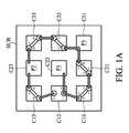
- FIG. 1Aillustrates an exemplary LED device that may be directly driven by a three-phase AC power source.
- FIG. 1BAn equivalent circuit diagram of the device in FIG. 1A is shown in FIG. 1B .
- FIG. 1Bshows that the circuit contains six groups of paired LEDs; the groups being designated C 11 , C 21 , C 12 , C 32 , C 13 , and C 33 .
- Each groupcontains a pair of LEDs connected in parallel and oriented so that when one LED is forward biased, the other LED is reverse biased.
- the term anti-parallelwill be used to refer to the arrangement of the LEDs in each group (i.e. connected in parallel and oppositely oriented).
- the circuitfurther includes paired LEDs C 22 , C 23 , and C 31 .
- the three-phase poweris connected to contact points P 1 , P 2 , and P 3 .
- the arrangement of LEDs in the circuiteliminates the need for a drive circuit.
- a voltage applied across serially connected LEDswill be distributed across the LEDs so that each LED sees only a fraction of the total voltage.
- the serial connection between the various LED groupslowers the high voltage applied at the contact points so that each of the individual LEDs is subjected to a lower voltage.
- the circuit in FIG. 1Bcan continuously produce light from AC power because the anti-parallel arrangement of the LEDs in each of the groups ensures that one of the LEDs in each group will produce light regardless of the polarity of the power applied to the pair, and the distribution of the groups among the contact points ensures that at least one of the pairs of groups will be subjected to a non-zero voltage from one of the three phases.
- the circuit shown in FIG. 1Ballows a high AC drive voltage to be used to drive LEDs that otherwise will not be able to stand the high voltage without an additional drive circuit.
- the device in FIG. 1Acontains the circuit from FIG. 1B monolithically formed on a single substrate.
- the six LED groups C 11 , C 21 , C 12 , C 32 , C 13 , and C 33 and the three power contact points P 1 , P 2 , and P 3are disposed on a single surface of substrate SUB.
- the device shown in FIG. 1Asuffers from drawbacks.
- FIG. 1Aillustrates that in order to accommodate the circuit, a relatively large area substrate SUB is needed. Therefore, it is hard to form a compact AC-powered LED device if the connection scheme as shown in FIG. 1A is adopted. The situation is further worsened when far more than two LED groups are connected in series in order to distribute the voltage of a higher voltage AC power source.
- a circuit structurein accordance with one aspect of the present invention, includes a carrier substrate, which includes a first through-via and a second through-via. Each of the first through-via and the second through-via extends from a first surface of the carrier substrate to a second surface of the carrier substrate opposite the first surface.
- the circuit structurefurther includes an LED chip bonded onto the first surface of the carrier substrate.
- the LED chipincludes a first electrode and a second electrode connected to the first through-via and the second through-via, respectively.
- a circuit structurein accordance with another aspect of the present invention, includes a carrier substrate, which includes first contact pads on a first surface of the carrier substrate; and second contact pads on a second surface of the carrier substrate opposite the first surface. Each of the second contact pads is connected to one of a first through-vias and a second through-vias.
- the circuit structurefurther includes through-vias extending from the first surface to the second surface of the carrier substrate, wherein each of the first contact pads and the second contact pads is connected to one of the through-vias; LED chips bonded onto the first surface of the carrier substrate, wherein each of the LED chips comprises a first electrode and a second electrode, each being connected to one of the first contact pads; and connection wires on the second surface of the carrier substrate and electrically interconnecting the LED chips.
- a circuit structurein accordance with yet another aspect of the present invention, includes a carrier substrate, which includes through-vias; and contact pads on a first surface of the carrier substrate, wherein each of the contact pads is connected to one of the through-vias.
- the circuit structurefurther includes LED chips bonded onto the first surface of the carrier substrate, wherein each of the LED chips includes a first electrode and a second electrode on a same surface, each being bonded to one of the contact pads through direct bonding; and a sacrificial substrate attached to the LED chips.
- the sacrificial substrateis on an opposite surface of the LED chips than the carrier substrate.
- the advantageous features of the present inventioninclude reduced area usage of the carrier substrate and reduced heat to affect LED chips.
- FIG. 1Aillustrates an LED device that can be driven by AC power
- FIG. 1Billustrates a circuit diagram of the device shown in FIG. 1A ;
- FIGS. 2 through 6are cross-sectional views of stages in the manufacturing of an embodiment of the present invention.
- FIG. 7Aillustrates a top view of an embodiment of the present invention
- FIG. 7Billustrates a circuit diagram of the embodiment shown in FIG. 7A .
- FIGS. 8 and 9illustrate alternative embodiments of the present invention.
- LEDslight-emitting diodes
- a devicecomprising several interconnected LEDs that is capable of being driven by an AC power source is used as an illustrative embodiment.
- the unique process steps required for manufacturing the illustrative embodimentare described. Those steps may be integrated in standard LED device fabrication processes.
- the making and using of the presently preferred embodimentsare discussed in detail below. It should be appreciated, however, that the present invention provides many applicable inventive concepts that can be embodied in a wide variety of specific contexts. The specific embodiments discussed are merely illustrative of specific ways to make and use the invention and do not limit the scope of the invention. Throughout the various views and illustrative embodiments of the present invention, like reference numbers are used to designate like elements.
- FIG. 2illustrates substrate 20 and group-III nitride (referred to as being III-nitride hereinafter) layers 22 formed on substrate 20 , wherein III-nitride layers 22 comprise the nitrides of group-III element(s).
- Substrate 20which is also referred to as being a sacrificial substrate, is preferably a silicon substrate having, for example, a (100), (110), or (111) surface orientation, although other substrates commonly used for forming III-nitride materials thereon, such as sapphire, silicon carbon, or the like, may also be used.
- III-nitride layers 22are used for forming LEDs.
- III-nitride layers 22include active layer 24 , which is used for emitting light, and other layers for supporting the operation of the respective LED devices, such as cladding layers.
- active layer 24As is known in the art, the layers overlying and underlying active layer 24 typically have opposite conductivity types.
- the III-nitride layers over active layer 24are referred to as upper III-nitride layers, while the III-nitride layers under the active layer 24 are referred to as lower III-nitride layers.
- III-nitride layers 22 and the underlying substrate 20are only weakly bonded together, which means that III-nitride layers 22 and the underlying substrate 20 may be separated in subsequent process steps without damaging either III-nitride layers 22 or substrate 20 .
- the weak bondingis formed through columns 21 with air-gaps 23 separating columns 21 from each other.
- III-nitride layers 22are then formed as continuous layers by means of the epitaxial lateral overgrowth (ELOG) technique, and hence air-gaps 23 are sealed under III-nitride layers 22 .
- the weak bondingcomprises a porous layer between substrate 20 and III-nitride layers 22 .
- the porous layermay be formed by converting a portion of substrate 20 to a porous layer.
- the porous layermay be formed by, for example, an electro-chemical anodization process using an electrolyte composition comprising an aqueous solution of hydrofluoric acid (about 20% by mass) and ethylic alcohol.
- the chemical anodization processmay be performed with an anodic current density of about 1 mA/cm 2 to about 200 mA/cm 2 .
- substrate 20Before forming the porous layer, substrate 20 may have a thickness greater than about 100 ⁇ m.
- the porous layermay have a thickness between about 10 ⁇ and about 1 ⁇ m.
- a plurality of upper electrodes/reflectors 26(referred to as reflectors 26 hereinafter), which are used for reflecting light, is formed over III-nitride layers 22 .
- Exemplary materials of reflectors 26include multi layers containing Ni/Au, titanium, titanium nitride, tantalum, tantalum nitride, or combinations thereof.
- Each of reflectors 26may also include a titanium nitride layer on a tantalum nitride layer, or a tantalum nitride layer on a titanium nitride layer.
- FIG. 3shows the patterning of the continuous III-nitride layers 22 from FIG. 2 .
- the patterning processemploys standard photolithographic and etching processes known in the art to expose the lower III-nitride layer.
- electrodes 30are then formed on the lower III-nitride layer.
- FIG. 3also shows the result of a separate patterning process in which III-nitride layers 22 are patterned to form a plurality of separate LED chips 34 . Each of the separate LED chips is activated by applying an appropriate voltage between its reflector 26 and other electrode 30 .
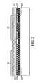
- FIG. 4illustrates carrier substrate 40 comprising a plurality of through-vias 42 .
- carrier substrate 40is a silicon substrate wherein each of through-vias 42 is a through-silicon via.
- carrier substrate 40is a printed circuit board (PCB) comprising a plurality of through-vias 42 .
- PCBprinted circuit board
- a plurality of contact pads 44 and 46are formed on the top and bottom surfaces of carrier substrate 40 , wherein each of the plurality of contact pads 44 on the top surface of the carrier substrate 40 is connected to one of the plurality of contact pads 46 on the bottom surface of the carrier substrate 40 through one of the plurality of through-vias 42 .
- electrical connections 50are bonded to some of contact pads 44 in order to interconnect desirable contact pads 44 .
- electrical connections 50comprise connection wires.
- the desirable contact pads 44may be electrically connected using other methods, such as conductive traces patterned onto the top surface of the carrier substrate.
- one of contact pads 46may be connected to one of contact pads 44 through a plurality of through-vias 42 .
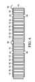
- FIG. 5shows the structure formed by flip-chip bonding carrier substrate 40 from FIG. 4 onto the combination of LED chips 34 and substrate 20 from FIG. 3 .
- connections 48are formed to connect the reflectors 26 to contact pads 46 on carrier substrate 40
- additional connections 51are formed to connect the other electrodes 30 to other contact pads 46 on the carrier substrate 40 .
- the connectionsare formed using standard flip-chip techniques.
- the connections ( 48 , 51 )may be formed using solder bonding, glue bonding, or direct metal-to-metal bonding, wherein a thin layer of solder or conductive glue (not shown) may be left between contact pads 46 and electrodes ( 30 , 48 ).
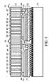
- substrate 20is separated from the rest of the structure as shown in FIG. 5 .
- the separationis performed by breaking the weak connection between substrate 20 and LED chips 34 .
- the weak connectionwhich may comprise columns 21 or a porous layer, is typically broken by an etch process, but it may be broken by other methods, such as mechanical cleaving.
- a residue of columns 21 or the porous layermay be generated.
- the residuemay be left without being removed and may improve the deflection of the light emitted by active layer 24 .
- Connection wires 50 or other types of electrical connectionsmay now be formed to interconnect LED chips 34 if they were not already interconnected in preceding steps.
- electrical connectionsmay also be formed using microelectronic processing techniques (such as deposition and patterning) instead of wire bonding during the process steps as shown in FIG. 4 .
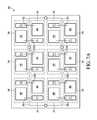
- FIG. 7Aillustrates a schematic view of a top surface of carrier substrate 40 that may be used in accordance with the previously described methods to create an equivalent circuit to that shown in FIG. 1B .
- the LED chipsare placed over the top surface of the carrier substrate, but in FIG. 7A , only the outline of LED chips 34 is shown as a dotted line so that the connections ( 48 , 51 ) between the electrodes on the LED chips and the contact pads ( 46 in FIG. 6 , not shown in FIG. 7A ) on the top surface of carrier substrate 40 can be seen.
- the connections ( 48 , 51 )are in turn electrically connected to the contact pads ( 44 in FIG. 6 , not shown in FIG.
- connection wires 50 that connect pairs of contact pads on the bottom surface of the substrateare shown, although they are on the opposite surface of carrier substrate 40 from LED chips 34 .
- power contact pointsP 1 , P 2 , and P 3 in FIG. 1B , not shown in FIG. 7A ) may also be placed on the opposite surface of the carrier substrate 40 from the LED chips 34 . Accordingly, LED chips 34 may be packaged tightly since the LED chips do not have to share one surface of carrier substrate 40 with the connection wires or power contact points. Therefore, the resulting LED device 60 is more compact than the device shown in FIG. 1A in which the area of carrier substrate 40 may be wasted due to the formation of contact pads and wiring between LED chips.
- FIG. 7Bis a circuit diagram of LED device 60 as shown in FIG. 7A .
- a significantly greater number of LED chipsmay be needed than shown in FIG. 7A .
- each of LED chips 34has a working voltage of 4 volts, then about 28 LED chips need to be connected in series in order for the device to be connected to a standard 110V AC power.
- the circuit shown in FIG. 7Balso illustrates that LED chips 34 may be grouped, with each group of LED chips 34 connected in series, with different groups being in anti-parallel orientation. That is, the head of the first group of LED chips is connected to the end of the second group of LED chips, and vice versa. Further, more connection wires 50 (marked as 50 ′) may be used to connect intermediate nodes in different groups of LED chips 34 .
- LED chips 34are connected to carrier substrate 40 using flip-chip technology, and substrate 20 on which LED chips 34 were fabricated is removed from the LED chips 34 .
- the LED chips 34may remain attached to the substrate on which they fabricated.
- LED chips 34are diced along with the underlying substrate 70 , and the completed LED chips 34 retain a portion of substrate 70 .
- the portion of LED chips 34 made up of substrate 70is bonded to carrier substrate 40 , while the active portion of LED chips 34 is electrically connected to carrier substrate 40 using wire bonding. This embodiment is compatible with LED chips 34 that are fabricated on an insulating substrate 70 .
- Each LED chip 34has two electrodes, 26 and 30 , electrically connected to the upper and lower III-nitride layers, respectively. In some embodiments it may be desirable to place a connection material 48 on top of one or both of the electrodes ( 26 , 30 ). Bonding wires 72 are used to connect electrodes 26 and 30 to contact pads 46 on the surface of carrier substrate 40 . Contact pads 46 are further connected to contact pads 44 on the other surface of carrier substrate 40 through through-vias 42 . Contacts pads 44 can be interconnected through connection wires 50 to form an equivalent device to that shown in FIGS. 7A and 7B .
- FIG. 9illustrates yet another embodiment of the present invention in which LED chips 34 retain a portion of substrate 80 on which they were fabricated.
- This embodimentis compatible with LED chips 34 that are fabricated on a conductive substrate 80 .
- substrate 80can provide an electrical connection to the lower III-nitride layer on LED chips 34 , so the substrate can be bonded on, and electrically connected to, contact pad 46 on the surface of carrier substrate 40 .
- Electrode 86connected to the upper III-nitride layer of LED chips 34 , can be electrically connected to other contact pads 46 on the same surface of the carrier substrate through bonding wires 72 .
- contact pads 46 on one surface of carrier substrate 40are connected to contact pads 44 on the other surface of carrier substrate 40 by through-vias 42 .
- Contacts pads 44 on the other surface of carrier substrate 40are further interconnected through connection wires 50 to form a completed LED device, such as an equivalent to the device shown in FIGS. 7A and 7B .
- the embodiments of the present inventionhave several advantageous features over LED devices that are completely fabricated on one surface of a carrier substrate.
- By bonding LED chips onto one surface of a carrier substrate and placing connection wires and external contact points on the other surface of the carrier substratesmaller area substrates may be employed to create more compact devices.
- By distributing the connection wires on an opposite surface of the carrier substrate than the LED chipsthe LED chips are affected less by the heat created by the contact resistance between the wiring and the contact pads.
- the process steps for forming the embodiments of the present inventionmay also benefit from using a silicon substrate as a base for forming LED chips due to the low cost of silicon substrates.
- the silicon substrate 20after being separated from carrier substrate 40 , may be reused.
- embodimentscould also integrate LED chips onto a semiconductor device by fabricating the device on one surface of a silicon substrate, fabricating through-silicon vias in the substrate, and bonding the LED chip onto the other surface of the silicon substrate.
- processes, machines, manufacture, compositions of matter, means, methods, or stepspresently existing or later to be developed, that perform substantially the same function or achieve substantially the same result as the corresponding embodiments described herein may be utilized according to the present invention. Accordingly, the appended claims are intended to include within their scope such processes, machines, manufacture, compositions of matter, means, methods, or steps.
Landscapes
- Engineering & Computer Science (AREA)
- Microelectronics & Electronic Packaging (AREA)
- Power Engineering (AREA)
- Physics & Mathematics (AREA)
- Condensed Matter Physics & Semiconductors (AREA)
- General Physics & Mathematics (AREA)
- Computer Hardware Design (AREA)
- Led Device Packages (AREA)
Abstract
Description
Claims (20)
Priority Applications (1)
| Application Number | Priority Date | Filing Date | Title |
|---|---|---|---|
| US13/269,968US8525216B2 (en) | 2008-08-28 | 2011-10-10 | Light-emitting diode integration scheme |
Applications Claiming Priority (3)
| Application Number | Priority Date | Filing Date | Title |
|---|---|---|---|
| US9248408P | 2008-08-28 | 2008-08-28 | |
| US12/535,525US8058669B2 (en) | 2008-08-28 | 2009-08-04 | Light-emitting diode integration scheme |
| US13/269,968US8525216B2 (en) | 2008-08-28 | 2011-10-10 | Light-emitting diode integration scheme |
Related Parent Applications (1)
| Application Number | Title | Priority Date | Filing Date |
|---|---|---|---|
| US12/535,525ContinuationUS8058669B2 (en) | 2008-08-28 | 2009-08-04 | Light-emitting diode integration scheme |
Publications (2)
| Publication Number | Publication Date |
|---|---|
| US20120025222A1 US20120025222A1 (en) | 2012-02-02 |
| US8525216B2true US8525216B2 (en) | 2013-09-03 |
Family
ID=41723968
Family Applications (2)
| Application Number | Title | Priority Date | Filing Date |
|---|---|---|---|
| US12/535,525Active2029-12-17US8058669B2 (en) | 2008-08-28 | 2009-08-04 | Light-emitting diode integration scheme |
| US13/269,968ActiveUS8525216B2 (en) | 2008-08-28 | 2011-10-10 | Light-emitting diode integration scheme |
Family Applications Before (1)
| Application Number | Title | Priority Date | Filing Date |
|---|---|---|---|
| US12/535,525Active2029-12-17US8058669B2 (en) | 2008-08-28 | 2009-08-04 | Light-emitting diode integration scheme |
Country Status (3)
| Country | Link |
|---|---|
| US (2) | US8058669B2 (en) |
| CN (1) | CN101667570B (en) |
| TW (1) | TWI393242B (en) |
Cited By (7)
| Publication number | Priority date | Publication date | Assignee | Title |
|---|---|---|---|---|
| US20140167093A1 (en)* | 2012-12-13 | 2014-06-19 | Hon Hai Precision Industry Co., Ltd. | Light emitting diode having a plurality of heat conductive columns |
| US20150144870A1 (en)* | 2012-07-26 | 2015-05-28 | Sang Jeong An | Semiconductor light-emitting device |
| US9224932B2 (en) | 2011-07-21 | 2015-12-29 | Tsmc Solid State Lighting Ltd. | Wafer level photonic device die structure and method of making the same |
| US9257623B2 (en) | 2014-02-17 | 2016-02-09 | Samsung Electronics Co., Ltd. | Light-emitting diode package |
| US9853197B2 (en)* | 2014-09-29 | 2017-12-26 | Bridgelux, Inc. | Light emitting diode package having series connected LEDs |
| US10263140B2 (en) | 2012-06-14 | 2019-04-16 | Sang Jeong An | Semiconductor light-emitting device and method for manufacturing the same |
| US20230187582A1 (en)* | 2020-03-09 | 2023-06-15 | Samsung Display Co., Ltd. | Display device |
Families Citing this family (30)
| Publication number | Priority date | Publication date | Assignee | Title |
|---|---|---|---|---|
| DE102008049188A1 (en)* | 2008-09-26 | 2010-04-01 | Osram Opto Semiconductors Gmbh | Optoelectronic module with a carrier substrate and a plurality of radiation-emitting semiconductor components and method for its production |
| TWI473246B (en)* | 2008-12-30 | 2015-02-11 | Epistar Corp | LED Diode Grade Package |
| TWI495084B (en)* | 2009-07-07 | 2015-08-01 | Epistar Corp | Light-emitting element |
| US8388469B1 (en) | 2009-11-18 | 2013-03-05 | Mark it Art, Inc. | Inlay golf ball marker |
| CN106298752A (en)* | 2010-04-15 | 2017-01-04 | 西铁城电子株式会社 | Light-emitting device |
| JP5426481B2 (en)* | 2010-05-26 | 2014-02-26 | 株式会社東芝 | Light emitting device |
| US9293678B2 (en)* | 2010-07-15 | 2016-03-22 | Micron Technology, Inc. | Solid-state light emitters having substrates with thermal and electrical conductivity enhancements and method of manufacture |
| US20120068218A1 (en)* | 2010-09-17 | 2012-03-22 | Taiwan Semiconductor Manufacturing Company, Ltd. | Thermally efficient packaging for a photonic device |
| CN102454878B (en)* | 2010-10-19 | 2014-07-02 | 展晶科技(深圳)有限公司 | Light-emitting diode module |
| US8653542B2 (en)* | 2011-01-13 | 2014-02-18 | Tsmc Solid State Lighting Ltd. | Micro-interconnects for light-emitting diodes |
| US8236584B1 (en) | 2011-02-11 | 2012-08-07 | Tsmc Solid State Lighting Ltd. | Method of forming a light emitting diode emitter substrate with highly reflective metal bonding |
| TWI517452B (en)* | 2011-03-02 | 2016-01-11 | 建準電機工業股份有限公司 | Polycrystalline package structure of luminescent crystal |
| JP5770006B2 (en)* | 2011-04-15 | 2015-08-26 | シチズン電子株式会社 | Semiconductor light emitting device |
| US8916968B2 (en) | 2012-03-27 | 2014-12-23 | Infineon Technologies Ag | Multichip power semiconductor device |
| CN103681644B (en)* | 2012-09-14 | 2016-08-17 | 晶元光电股份有限公司 | High-voltage LEDs with improved heat dissipation and light extraction |
| KR102065390B1 (en)* | 2013-02-15 | 2020-01-13 | 엘지이노텍 주식회사 | Light emitting device, light emitting device package, and light unit |
| DE102013202904A1 (en)* | 2013-02-22 | 2014-08-28 | Osram Opto Semiconductors Gmbh | Optoelectronic semiconductor component and method for its production |
| FR3011388B1 (en)* | 2013-09-30 | 2016-11-25 | Aledia | OPTOELECTRONIC DEVICE WITH LIGHT EMITTING DIODES |
| US10234119B2 (en)* | 2014-03-24 | 2019-03-19 | Cree, Inc. | Multiple voltage light emitter packages, systems, and related methods |
| TWI630734B (en)* | 2014-06-30 | 2018-07-21 | 億光電子工業股份有限公司 | Light emitting diode device |
| TWI556478B (en)* | 2014-06-30 | 2016-11-01 | 億光電子工業股份有限公司 | Light-emitting diode device |
| DE102014219126A1 (en)* | 2014-09-23 | 2016-03-24 | Continental Automotive Gmbh | Arrangement with circuit carrier for an electronic device |
| WO2016076637A1 (en)* | 2014-11-12 | 2016-05-19 | Seoul Viosys Co., Ltd. | Light emitting device |
| JP6156402B2 (en) | 2015-02-13 | 2017-07-05 | 日亜化学工業株式会社 | Light emitting device |
| US9583912B2 (en) | 2015-05-20 | 2017-02-28 | Hc Photonics Corp. | Compact optical and laser systems and ultrafast laser utilizing the same |
| CN105489727B (en)* | 2016-01-18 | 2018-06-19 | 厦门市三安光电科技有限公司 | The bonding electrode structure and production method of flip LED chips |
| DE102018127075B4 (en)* | 2018-10-30 | 2021-12-30 | Auto-Kabel Management Gmbh | High current circuit |
| WO2021013463A1 (en)* | 2019-07-23 | 2021-01-28 | Lumileds Holding B.V. | Semiconductor light-emitting device |
| TWI760103B (en)* | 2021-02-09 | 2022-04-01 | 國立臺灣科技大學 | Adjustable optical phase array |
| US12213240B2 (en)* | 2022-09-16 | 2025-01-28 | Hamilton Sundstrand Corporation | Pin-fin cooling for printed circuit boards (PCBs) |
Citations (15)
| Publication number | Priority date | Publication date | Assignee | Title |
|---|---|---|---|---|
| US6538309B1 (en)* | 1999-03-29 | 2003-03-25 | Nitto Denko Corporation | Semiconductor device and circuit board for mounting semiconductor element |
| US20050253151A1 (en) | 2002-08-29 | 2005-11-17 | Shiro Sakai | Light-emitting device having light-emitting elements |
| WO2006005062A2 (en) | 2004-06-30 | 2006-01-12 | Cree, Inc. | Chip-scale methods for packaging light emitting devices and chip-scale packaged light emitting devices |
| US20070138495A1 (en) | 2005-12-09 | 2007-06-21 | Industrial Technology Research Institute | AC_LED System in Single Chip with Three Metal Contacts |
| US20070145383A1 (en) | 2005-11-10 | 2007-06-28 | Samsung Electronics Co., Ltd. | High luminance light emitting diode and liquid crystal display device using the same |
| US7436000B2 (en)* | 2005-01-26 | 2008-10-14 | Samsung Electronics Co., Ltd. | Two dimensional light source using light emitting diode and liquid crystal display device using the two dimensional light source |
| US7470926B2 (en) | 2004-09-09 | 2008-12-30 | Toyoda Gosei Co., Ltd | Solid-state optical device |
| US7550319B2 (en)* | 2005-09-01 | 2009-06-23 | E. I. Du Pont De Nemours And Company | Low temperature co-fired ceramic (LTCC) tape compositions, light emitting diode (LED) modules, lighting devices and method of forming thereof |
| US7626208B2 (en)* | 2006-03-17 | 2009-12-01 | Industrial Technology Research Institute | Bendable solid state planar light source structure |
| US7825423B2 (en)* | 2006-02-02 | 2010-11-02 | Shinko Electric Industries Co., Ltd. | Semiconductor device and method of manufacturing semiconductor device |
| US7872279B2 (en)* | 2007-05-23 | 2011-01-18 | Advanced Connectek Inc. | Light-emitting diode package |
| US7875897B2 (en)* | 2004-09-09 | 2011-01-25 | Toyoda Gosei Co., Ltd. | Light emitting device |
| US7875533B2 (en)* | 2004-10-28 | 2011-01-25 | Koninklijke Philips Electronics N.V. | Package-integrated thin film LED |
| US7902568B2 (en)* | 2005-07-15 | 2011-03-08 | Panasonic Corporation | Light-emitting module with plural light emitters and conductor pattern |
| US7977686B2 (en)* | 2005-06-30 | 2011-07-12 | Cree, Inc. | Chip-scale methods for packaging light emitting devices and chip-scale packaged light emitting devices |
- 2009
- 2009-08-04USUS12/535,525patent/US8058669B2/enactiveActive
- 2009-08-28CNCN200910163585.8Apatent/CN101667570B/enactiveActive
- 2009-08-28TWTW098128999Apatent/TWI393242B/enactive
- 2011
- 2011-10-10USUS13/269,968patent/US8525216B2/enactiveActive
Patent Citations (19)
| Publication number | Priority date | Publication date | Assignee | Title |
|---|---|---|---|---|
| US6538309B1 (en)* | 1999-03-29 | 2003-03-25 | Nitto Denko Corporation | Semiconductor device and circuit board for mounting semiconductor element |
| US20050253151A1 (en) | 2002-08-29 | 2005-11-17 | Shiro Sakai | Light-emitting device having light-emitting elements |
| WO2006005062A2 (en) | 2004-06-30 | 2006-01-12 | Cree, Inc. | Chip-scale methods for packaging light emitting devices and chip-scale packaged light emitting devices |
| CN101032034A (en) | 2004-06-30 | 2007-09-05 | 克里公司 | Chip-scale methods for packaging light emitting devices and chip-scale packaged light emitting devices |
| US7329905B2 (en)* | 2004-06-30 | 2008-02-12 | Cree, Inc. | Chip-scale methods for packaging light emitting devices and chip-scale packaged light emitting devices |
| US7667223B2 (en)* | 2004-09-09 | 2010-02-23 | Toyoda Gosei Co., Ltd. | Solid-state optical device |
| US7875897B2 (en)* | 2004-09-09 | 2011-01-25 | Toyoda Gosei Co., Ltd. | Light emitting device |
| US7470926B2 (en) | 2004-09-09 | 2008-12-30 | Toyoda Gosei Co., Ltd | Solid-state optical device |
| US7875533B2 (en)* | 2004-10-28 | 2011-01-25 | Koninklijke Philips Electronics N.V. | Package-integrated thin film LED |
| US7436000B2 (en)* | 2005-01-26 | 2008-10-14 | Samsung Electronics Co., Ltd. | Two dimensional light source using light emitting diode and liquid crystal display device using the two dimensional light source |
| US7977686B2 (en)* | 2005-06-30 | 2011-07-12 | Cree, Inc. | Chip-scale methods for packaging light emitting devices and chip-scale packaged light emitting devices |
| US7902568B2 (en)* | 2005-07-15 | 2011-03-08 | Panasonic Corporation | Light-emitting module with plural light emitters and conductor pattern |
| US7550319B2 (en)* | 2005-09-01 | 2009-06-23 | E. I. Du Pont De Nemours And Company | Low temperature co-fired ceramic (LTCC) tape compositions, light emitting diode (LED) modules, lighting devices and method of forming thereof |
| US20070145383A1 (en) | 2005-11-10 | 2007-06-28 | Samsung Electronics Co., Ltd. | High luminance light emitting diode and liquid crystal display device using the same |
| US7868332B2 (en)* | 2005-11-10 | 2011-01-11 | Samsung Electronics Co., Ltd. | High luminance light emitting diode and liquid crystal display device using the same |
| US20070138495A1 (en) | 2005-12-09 | 2007-06-21 | Industrial Technology Research Institute | AC_LED System in Single Chip with Three Metal Contacts |
| US7825423B2 (en)* | 2006-02-02 | 2010-11-02 | Shinko Electric Industries Co., Ltd. | Semiconductor device and method of manufacturing semiconductor device |
| US7626208B2 (en)* | 2006-03-17 | 2009-12-01 | Industrial Technology Research Institute | Bendable solid state planar light source structure |
| US7872279B2 (en)* | 2007-05-23 | 2011-01-18 | Advanced Connectek Inc. | Light-emitting diode package |
Cited By (10)
| Publication number | Priority date | Publication date | Assignee | Title |
|---|---|---|---|---|
| US9224932B2 (en) | 2011-07-21 | 2015-12-29 | Tsmc Solid State Lighting Ltd. | Wafer level photonic device die structure and method of making the same |
| US9502627B2 (en) | 2011-07-21 | 2016-11-22 | Epistar Corporation | Wafer level photonic devices dies structure and method of making the same |
| US10263140B2 (en) | 2012-06-14 | 2019-04-16 | Sang Jeong An | Semiconductor light-emitting device and method for manufacturing the same |
| US20150144870A1 (en)* | 2012-07-26 | 2015-05-28 | Sang Jeong An | Semiconductor light-emitting device |
| US9362446B2 (en)* | 2012-07-26 | 2016-06-07 | Sang Jeong An | Semiconductor light-emitting device |
| US20140167093A1 (en)* | 2012-12-13 | 2014-06-19 | Hon Hai Precision Industry Co., Ltd. | Light emitting diode having a plurality of heat conductive columns |
| US9257623B2 (en) | 2014-02-17 | 2016-02-09 | Samsung Electronics Co., Ltd. | Light-emitting diode package |
| US9853197B2 (en)* | 2014-09-29 | 2017-12-26 | Bridgelux, Inc. | Light emitting diode package having series connected LEDs |
| US10230035B2 (en) | 2014-09-29 | 2019-03-12 | Bridgelux, Inc. | Light emitting diode package having series connected LEDs |
| US20230187582A1 (en)* | 2020-03-09 | 2023-06-15 | Samsung Display Co., Ltd. | Display device |
Also Published As
| Publication number | Publication date |
|---|---|
| US20120025222A1 (en) | 2012-02-02 |
| TWI393242B (en) | 2013-04-11 |
| US8058669B2 (en) | 2011-11-15 |
| US20100051972A1 (en) | 2010-03-04 |
| CN101667570B (en) | 2013-02-20 |
| CN101667570A (en) | 2010-03-10 |
| TW201010048A (en) | 2010-03-01 |
Similar Documents
| Publication | Publication Date | Title |
|---|---|---|
| US8525216B2 (en) | Light-emitting diode integration scheme | |
| US12199082B2 (en) | Method of direct-bonded optoelectronic devices | |
| TWI691046B (en) | Micro-led display assembly | |
| TWI440210B (en) | Illumination device using external interconnection array of light-emitting device and manufacturing method thereof | |
| CN102810619B (en) | led | |
| US20120286240A1 (en) | Methods of Fabricating Light Emitting Diode Packages | |
| JP2011129920A (en) | Light emitting element and method of manufacturing the same | |
| TW201114003A (en) | Chip package structure and method for fabricating the same | |
| CN115152019A (en) | Multi-wavelength light emitting element and method for manufacturing same | |
| US11728225B2 (en) | Micro LED verification substrate, manufacturing method therefor, and micro LED verification method using same | |
| US8841172B2 (en) | Method for forming package substrate | |
| CN108028261A (en) | Luminescent device and the method for manufacturing luminescent device | |
| US9666558B2 (en) | Substrate for mounting a chip and chip package using the substrate | |
| CN102376864B (en) | Light emitting element | |
| CN117253956A (en) | Micro LED display chip with multilayer film structure and preparation method thereof | |
| TW201203611A (en) | Light emitting device and its manufacturing method | |
| CN113284991A (en) | Micro LED chip, packaging method thereof and electronic device | |
| CN108028250B (en) | LED light source comprising an electronic circuit | |
| TWI532225B (en) | Multi - grain cladding module packaging method | |
| KR102198918B1 (en) | Metal substrate for led | |
| WO2024087427A1 (en) | Small light-emitting diode (led) module and preparation method therefor | |
| TWI555241B (en) | A light emitting diode array structure |
Legal Events
| Date | Code | Title | Description |
|---|---|---|---|
| STCF | Information on status: patent grant | Free format text:PATENTED CASE | |
| AS | Assignment | Owner name:TAIWAN SEMICONDUCTOR MANUFACTURING COMPANY, LTD., Free format text:ASSIGNMENT OF ASSIGNORS INTEREST;ASSIGNORS:CHEN, DING-YUAN;CHIOU, WEN-CHIH;YU, CHEN-HUA;REEL/FRAME:035416/0859 Effective date:20090806 | |
| AS | Assignment | Owner name:CHIP STAR LTD., TAIWAN Free format text:ASSIGNMENT OF ASSIGNORS INTEREST;ASSIGNOR:TAIWAN SEMICONDUCTOR MANUFACTURING COMPANY, LTD.;REEL/FRAME:036543/0245 Effective date:20150624 | |
| AS | Assignment | Owner name:EPISTAR CORPORATION, TAIWAN Free format text:MERGER;ASSIGNOR:CHIP STAR LTD.;REEL/FRAME:037457/0645 Effective date:20150715 | |
| FPAY | Fee payment | Year of fee payment:4 | |
| MAFP | Maintenance fee payment | Free format text:PAYMENT OF MAINTENANCE FEE, 8TH YEAR, LARGE ENTITY (ORIGINAL EVENT CODE: M1552); ENTITY STATUS OF PATENT OWNER: LARGE ENTITY Year of fee payment:8 | |
| MAFP | Maintenance fee payment | Free format text:PAYMENT OF MAINTENANCE FEE, 12TH YEAR, LARGE ENTITY (ORIGINAL EVENT CODE: M1553); ENTITY STATUS OF PATENT OWNER: LARGE ENTITY Year of fee payment:12 |