US8524578B1 - Method and surface morphology of non-polar gallium nitride containing substrates - Google Patents
Method and surface morphology of non-polar gallium nitride containing substratesDownload PDFInfo
- Publication number
- US8524578B1 US8524578B1US13/548,770US201213548770AUS8524578B1US 8524578 B1US8524578 B1US 8524578B1US 201213548770 AUS201213548770 AUS 201213548770AUS 8524578 B1US8524578 B1US 8524578B1
- Authority
- US
- United States
- Prior art keywords
- plane
- polar
- oriented crystalline
- gallium
- hillocks
- Prior art date
- Legal status (The legal status is an assumption and is not a legal conclusion. Google has not performed a legal analysis and makes no representation as to the accuracy of the status listed.)
- Expired - Fee Related
Links
Images


Classifications
- H—ELECTRICITY
- H10—SEMICONDUCTOR DEVICES; ELECTRIC SOLID-STATE DEVICES NOT OTHERWISE PROVIDED FOR
- H10H—INORGANIC LIGHT-EMITTING SEMICONDUCTOR DEVICES HAVING POTENTIAL BARRIERS
- H10H20/00—Individual inorganic light-emitting semiconductor devices having potential barriers, e.g. light-emitting diodes [LED]
- H10H20/80—Constructional details
- H10H20/81—Bodies
- H10H20/817—Bodies characterised by the crystal structures or orientations, e.g. polycrystalline, amorphous or porous
- H—ELECTRICITY
- H01—ELECTRIC ELEMENTS
- H01S—DEVICES USING THE PROCESS OF LIGHT AMPLIFICATION BY STIMULATED EMISSION OF RADIATION [LASER] TO AMPLIFY OR GENERATE LIGHT; DEVICES USING STIMULATED EMISSION OF ELECTROMAGNETIC RADIATION IN WAVE RANGES OTHER THAN OPTICAL
- H01S5/00—Semiconductor lasers
- H01S5/30—Structure or shape of the active region; Materials used for the active region
- H01S5/32—Structure or shape of the active region; Materials used for the active region comprising PN junctions, e.g. hetero- or double- heterostructures
- H01S5/3202—Structure or shape of the active region; Materials used for the active region comprising PN junctions, e.g. hetero- or double- heterostructures grown on specifically orientated substrates, or using orientation dependent growth
- H01S5/32025—Structure or shape of the active region; Materials used for the active region comprising PN junctions, e.g. hetero- or double- heterostructures grown on specifically orientated substrates, or using orientation dependent growth non-polar orientation
- H—ELECTRICITY
- H01—ELECTRIC ELEMENTS
- H01S—DEVICES USING THE PROCESS OF LIGHT AMPLIFICATION BY STIMULATED EMISSION OF RADIATION [LASER] TO AMPLIFY OR GENERATE LIGHT; DEVICES USING STIMULATED EMISSION OF ELECTROMAGNETIC RADIATION IN WAVE RANGES OTHER THAN OPTICAL
- H01S2304/00—Special growth methods for semiconductor lasers
- H01S2304/04—MOCVD or MOVPE
- H—ELECTRICITY
- H01—ELECTRIC ELEMENTS
- H01S—DEVICES USING THE PROCESS OF LIGHT AMPLIFICATION BY STIMULATED EMISSION OF RADIATION [LASER] TO AMPLIFY OR GENERATE LIGHT; DEVICES USING STIMULATED EMISSION OF ELECTROMAGNETIC RADIATION IN WAVE RANGES OTHER THAN OPTICAL
- H01S5/00—Semiconductor lasers
- H01S5/30—Structure or shape of the active region; Materials used for the active region
- H01S5/32—Structure or shape of the active region; Materials used for the active region comprising PN junctions, e.g. hetero- or double- heterostructures
- H01S5/323—Structure or shape of the active region; Materials used for the active region comprising PN junctions, e.g. hetero- or double- heterostructures in AIIIBV compounds, e.g. AlGaAs-laser, InP-based laser
- H01S5/32308—Structure or shape of the active region; Materials used for the active region comprising PN junctions, e.g. hetero- or double- heterostructures in AIIIBV compounds, e.g. AlGaAs-laser, InP-based laser emitting light at a wavelength less than 900 nm
- H01S5/32341—Structure or shape of the active region; Materials used for the active region comprising PN junctions, e.g. hetero- or double- heterostructures in AIIIBV compounds, e.g. AlGaAs-laser, InP-based laser emitting light at a wavelength less than 900 nm blue laser based on GaN or GaP
- H—ELECTRICITY
- H10—SEMICONDUCTOR DEVICES; ELECTRIC SOLID-STATE DEVICES NOT OTHERWISE PROVIDED FOR
- H10H—INORGANIC LIGHT-EMITTING SEMICONDUCTOR DEVICES HAVING POTENTIAL BARRIERS
- H10H20/00—Individual inorganic light-emitting semiconductor devices having potential barriers, e.g. light-emitting diodes [LED]
- H10H20/80—Constructional details
- H10H20/81—Bodies
- H10H20/822—Materials of the light-emitting regions
- H10H20/824—Materials of the light-emitting regions comprising only Group III-V materials, e.g. GaP
- H10H20/825—Materials of the light-emitting regions comprising only Group III-V materials, e.g. GaP containing nitrogen, e.g. GaN
Definitions
- the present inventionis directed to optical devices and related methods. More particularly, the present invention provides a method and device for fabricating crystalline films for emitting electromagnetic radiation using non-polar gallium containing substrates such as GaN, MN, InN, InGaN, AlGaN, and AlInGaN, and others.
- the inventioncan be applied to optical devices, lasers, light emitting diodes, solar cells, photoelectrochemical water splitting and hydrogen generation, photodetectors, integrated circuits, and transistors, among other devices.
- the conventional light bulbcommonly called the “Edison bulb,” has been used for over one hundred years for a variety of applications including lighting and displays.
- the conventional light bulbuses a tungsten filament enclosed in a glass bulb sealed in a base, which is screwed into a socket.
- the socketis coupled to an AC power or DC power source.
- the conventional light bulbcan be found commonly in houses, buildings, and outdoor lightings, and other areas requiring light or displays. Unfortunately, drawbacks exist with the conventional Edison light bulb.
- the conventional light bulbdissipates much thermal energy. More than 90% of the energy used for the conventional light bulb dissipates as thermal energy.
- light bulbsemit in all directions and are not ideal for applications requiring strong directionality or focus such as projection displays, optical data storage, or specialized directed lighting.
- Theodore H. Maimandemonstrated the first laser at Hughes Research Laboratories in Malibu. This laser utilized a solid-state flashlamp-pumped synthetic ruby crystal to produce red laser light at 694 nm.
- blue and green laser outputwas demonstrated by William Bridges at Hughes Aircraft utilizing a gas laser design called an Argon ion laser.
- the Ar-ion laserutilized a noble gas as the active medium and produce laser light output in the UV, blue, and green wavelengths including 351 nm, 454.6 nm, 457.9 nm, 465.8 nm, 476.5 nm, 488.0 nm, 496.5 nm, 501.7 nm, 514.5 nm, and 528.7 nm.
- the Ar-ion laserhad the benefit of producing highly directional and focusable light with a narrow spectral output, but the wall plug efficiency was ⁇ 0.1%, and the size, weight, and cost of the lasers were undesirable as well.
- lamp pumped solid state laserswere developed in the infrared, and the output wavelength was converted to the visible using specialty crystals with nonlinear optical properties.
- a green lamp pumped solid state laserhad 3 stages: electricity powers lamp, lamp excites gain crystal which lases at 1064 nm, 1064 nm goes into frequency conversion crystal which converts to visible 532 nm.
- the resulting green and blue laserswere called “lamped pumped solid state lasers with second harmonic generation” (LPSS with SHG) had wall plug efficiency of ⁇ 1%, and were more efficient than Ar-ion gas lasers, but were still too inefficient, large, expensive, fragile for broad deployment outside of specialty scientific and medical applications. Additionally, the gain crystal used in the solid state lasers typically had energy storage properties which made the lasers difficult to modulate at high speeds which limited its broader deployment.
- DPSS with SHGhigh power diode (or semiconductor) lasers were utilized.
- These “diode pumped solid state lasers with SHG”had 3 stages: electricity powers 808 nm diode laser, 808 nm excites gain crystal which lases at 1064 nm, 1064 nm goes into frequency conversion crystal which converts to visible 532 nm.
- the DPSS laser technologyextended the life and improved the wall plug efficiency of the LPSS lasers to 5-10%, and further commercialization ensue into more high end specialty industrial, medical, and scientific applications.
- the change to diode pumpingincreased the system cost and required precise temperature controls, leaving the laser with substantial size, power consumption while not addressing the energy storage properties which made the lasers difficult to modulate at high speeds.
- the present inventionprovides a method and device for fabricating crystalline films for emitting electromagnetic radiation using non-polar gallium containing substrates such as GaN, MN, InN, InGaN, AlGaN, and AlInGaN, and others.
- the inventioncan be applied to optical devices, lasers, light emitting diodes, solar cells, photoelectrochemical water splitting and hydrogen generation, photodetectors, integrated circuits, and transistors, among other devices.
- the optical deviceis a laser that has been configured for blue and green emissions, as well as others.
- the optical deviceis an LED that has been configured for blue emission, as well as others.
- the present inventionprovides a method and resulting nonpolar m-plane (10-10) oriented gallium nitride structure (e.g., gallium and nitrogen containing structure, gallium nitride structure) having smooth surface morphology, which is often substantially free from hillocks and the like.
- the methodincludes using a miscut or offcut surface or no miscut or offcut or other off-axis orientation of a non-polar m-plane surface orientation as a growth surface region.
- the epitaxial layeris configured using at least an atmospheric pressure (e.g. 700-800 Torr) epitaxial formation process, but may also be configured for other processes.
- the methodincludes use of a N 2 carrier and subflow gas, which is substantially all N 2 , as a medium for precursor gases, which form the crystalline gallium nitride epitaxial material (e.g., gallium and nitrogen containing epitaxial material).
- a N 2 carrier and subflow gaswhich is substantially all N 2
- precursor gaseswhich form the crystalline gallium nitride epitaxial material (e.g., gallium and nitrogen containing epitaxial material).
- the growth using the substantially predominant N 2 gasleads to formation of crystalline gallium nitride epitaxial material substantially free of hillocks and the like.
- nonpolar (10-10) oriented gallium nitride structurerefers to the family of nonpolar m-plane (10-10) oriented gallium nitride structures, nonpolar m-plane (10-10) oriented gallium and nitrogen containing structures, and the like.
- the present inventionincludes use of a gallium nitride substrate configured in a non-polar (10-10) surface orientation that has a miscut towards the c-plane (0001) ranging from about ⁇ 0.6 degrees to about ⁇ 2.0 degrees and any miscut towards the a-plane (11-20) although there can be other orientations and degrees of miscut or offcut or off-axis orientation.
- the methoduses an H 2 carrier gas and combination of H 2 and N 2 subflow gases in further combination with precursor gases for growth of crystalline gallium nitride epitaxial material.
- the miscutcan be about ⁇ 0.8 degrees to about ⁇ 1.1 degrees toward the c-plane (0001) and between ⁇ 0.3 degrees and 0.3 degrees towards the a-plane (11-20) to cause formation of an overlying gallium nitride epitaxial layer with smooth morphology.
- the miscutcan be about ⁇ 0.8 degrees to about ⁇ 1.1 degrees toward the c-plane (0001) and between ⁇ 0.3 degrees and 0.3 degrees towards the a-plane (11-20) to cause formation of an overlying gallium nitride epitaxial layer with smooth morphology.
- the present inventionprovides an optical device that has epitaxial film that is substantially free from morphological features on the surface such as hillocks and the like.
- the devicehas a non-polar (10-10) gallium nitride substrate member having a slightly off-axis non-polar oriented crystalline surface plane.
- the slightly off-axis (or on-axis) non-polar oriented crystalline surface planeranges from about 0 degrees to a predetermined degree toward either or both the c-plane and/or a-plane.
- the devicehas a gallium nitride containing epitaxial layer formed overlying the slightly off-axis non-polar oriented crystalline surface plane.
- a surface regionis overlying the gallium nitride epitaxial layer.
- the surface regionbeing substantially free from hillocks having an average spatial dimension of, for example, 10-100 microns and greater, but can be other dimensions.
- the epitaxial layeris configured using at least an atmospheric pressure (e.g. 700-800 Torr) epitaxial formation process.
- the epitaxial layercomprises one or more layers which form at least a quantum well of at least 3.5 nanometers and greater or other desirable dimensions. The quantum well, which is thicker, leads to improved laser devices.
- the present inventionprovides a method of fabricating an optical device.
- the methodincludes providing a non-polar (10-10) gallium nitride substrate member having a slightly off-axis non-polar oriented crystalline surface plane.
- the slightly off-axis non-polar oriented crystalline surface planeis greater in magnitude than about negative 0.6 degrees toward the c-plane (0001) or other desirable magnitudes.
- the methodincludes forming a gallium nitride containing epitaxial layer having a smooth surface region substantially free of hillocks overlying the slightly off-axis non-polar oriented crystalline surface plane.
- the present inventionprovides a method of fabricating an alternative optical device.
- the methodincludes providing a non-polar (10-10) gallium nitride substrate member having a slightly off-axis non-polar oriented crystalline surface plane in a specific embodiment.
- the slightly off-axis non-polar oriented crystalline surface planeranges from about 0 degrees to a predetermined degree toward either or both the c-plane or a-plane.
- the present methodincludes forming a gallium nitride containing epitaxial layer, using at least an atmospheric pressure (e.g. 700-800 Torr) epitaxial process to form at least a quantum well having a thickness of at least 3.5 nanometers and greater or other desirable dimensions.
- the gallium nitride epitaxial layerhas a surface region substantially smooth and free from hillocks.
- miscutshould be interpreted according to ordinary meaning understood by one of ordinary skill in the art and does not imply a specific process to achieve the orientation.
- the term miscutis not intended to imply any undesirable cut relative to, for example, any of the crystal planes, e.g., c-plane, a-plane.
- miscutis intended to describe a surface orientation slightly tilted with respect to the primary surface crystal plane such as the nonpolar (10-10) GaN plane.
- offcutor “off-axis” is intended to have a similar meaning as miscut that does not imply any process to achieve the orientation, although there could be other variations, modifications, and alternatives.
- the crystalline surface planeis not miscut and/or offcut and/or off-axis but can be configured using a mechanical and/or chemical and/or physical process to expose any one of the crystalline surfaces described explicitly and/or implicitly herein.
- the terms miscut and/or offcut and/or off-axisare characterized by at least one or more directions and corresponding magnitudes, although there can be other variations, modifications, and alternatives.
- the present inventionenables a cost-effective technique for growth of large area crystals of non-polar materials, including GaN, AN, InN, InGaN, and AlInGaN and others and other gallium and nitrogen containing materials.
- the present method and resulting structureare relatively simple and cost effective to manufacture for commercial applications.
- a specific embodimentalso takes advantage of a combination of techniques, which solve a long standing need.
- the (10-10) non-polar substrate and overlying epitaxial crystalline gallium nitride containing filmare smooth and substantially free from hillocks and the like, which improve device performance.
- smoothgenerally means substantially free from hillocks or other surface imperfections, which lead to degradation in device performance, including reliability, intensity, efficiency, and other parameters that generally define performance.
- smoothwould also include other interpretations known by one of ordinary skill in the art, as well as variations, modifications, and alternatives. Depending upon the embodiment, one or more of these benefits may be achieved.
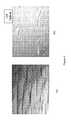
- FIG. 1( a )is an optical micrograph image representative of a conventional surface region including hillock structures on a non-polar GaN substrate.
- FIG. 1( b )is a schematic illustration of a top down view of a hillock structure.
- FIG. 1( c )is a schematic illustration of a cross-sectional view of a hillock structure.
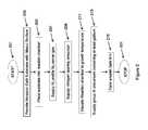
- FIG. 2is a simplified flow diagram of a method for fabricating an improved GaN film according to an embodiment of the present invention.
- FIG. 3is a simplified diagram illustrating various miscuts/offcuts in +/ ⁇ c/a planes according to one or more embodiments of the present invention
- FIGS. 4 through 6are photographs illustrating the improved GaN film according to an embodiment of the present invention.
- the present inventionprovides a method and device for fabricating crystalline films for emitting electromagnetic radiation using non-polar (10-10) gallium containing substrates such as GaN, MN, InN, InGaN, AlGaN, and AlInGaN, and others.
- non-polar (10-10) gallium containing substratessuch as GaN, MN, InN, InGaN, AlGaN, and AlInGaN, and others.
- the inventioncan be applied to optical devices, lasers, light emitting diodes, solar cells, photoelectrochemical water splitting and hydrogen generation, photodetectors, integrated circuits, and transistors, among other devices.
- the present inventionis directed to generate high efficiency GaN-based light emitting devices operating at wavelengths beyond 400 nm for blue, green, yellow and red emission according to embodiments of the present invention.
- the proposed devicewill be used as an optical source for various commercial, industrial, or scientific applications. These structures are expected to find utility in existing applications where blue-violet, blue, green, yellow and red laser/LED emission is required.
- An existing applicationincludes HD-DVD and Sony Blu-RayTM players.
- One particularly promising application for these devicesis full color displays requiring red-green-blue or blue-yellow color mixing.
- Another potential applicationis for optical communication through polymer based fibers where increased wavelengths will result in reduced loss.
- the present inventionprovides a GaN-based semiconductor laser/LED growth/fabrication method to achieve increased wavelength operation into the blue, green, yellow and red regime on nonpolar GaN substrates where superior laser/LED performance can be expected according to a specific embodiment.
- the devicerelies on smooth surface region films of epitaxial crystalline GaN containing materials for improved device performance.
- the smooth surface region and therefore higher quality crystalline materialcan be derived from epitaxial growth techniques according to one or more embodiments.
- Epitaxial growth on the nonpolar (10-10) plane of bulk GaNhas been emerging and possesses various limitations. Understanding growth parameter space for optimal epitaxial layer deposition is often important for the realization of high performance electronic on optoelectronic devices fabricated from the epitaxial layers. At least one key aspect of the film quality is the morphology. Morphology manifests itself in large scale features that are on the order of 10s to 100s of microns all the way down to the atomic scale on the order of Angstroms. Achieving smooth epitaxial layers on both the large scale and small scale often translate into high performance devices.
- FIG. 1( a )is an optical micrograph image which represents a conventional surface region of a non-polar (10-10) oriented gallium nitride epitaxial layer, including hillock structures.
- the surface shownis representative of epitaxial deposition at atmospheric pressure conditions (e.g. 700-800 Torr) on a non-polar (10-10) GaN substrate.
- non-polar GaNcan exhibit very distinct large-scale features referred to herein as hillocks.
- FIG. 1( b ) and FIG. 1( c )are schematic illustrations of a top-down and cross-sectional view of such a hillock feature.
- these hillocksare pyramidal in shape and typically elongated in the in the positive and negative a-directions and can demonstrate significantly steep sidewalls in the positive and negative c-directions.
- Schematic illustration of a top-down view of a pyramidal hillock structureis provided in FIG. 1( b ).
- shaded regionsrepresent faces of such a hillock structure which are inclined toward the c+ and c ⁇ directions
- white regions labeled “a”represent faces of such a hillock structure which are symmetrically inclined toward the a+/a ⁇ direction.
- Such hillocksare typically elongated in the +/ ⁇ a direction such that the lateral dimension x is larger than the corresponding perpendicular width dimension y as shown.
- the hillockscan range from 50-100 microns or greater.
- the hillockscan have a height scale on the orders of hundreds of nanometers, therefore they can be disruptive/detrimental to optoelectronic devices such as laser diodes since the cladding layers will have varying thickness along the cavity and the gain layers between the cladding layers can have sharp interfaces.
- the large-scale morphological featuresare predominantly “pyramidal hillocks” or like structures. These characteristics can lead to increased loss in optical devices such as lasers, reduced gain, and perhaps reduced yield and reliability. Of course, there can also be other limitations.
- a method according to one or more embodiments for forming a smooth epitaxial film using an offcut or miscut or off-axis substrateis briefly outlined below.
- the present inventionprovides a method and resulting crystalline epitaxial material with a surface region that is substantially smooth and free from hillocks and the like for improved device performance.
- the abovehas been described in terms of an off-axis surface configuration, there can be other embodiments having an on-axis configuration using one or more selected process recipes, which have been described in more detail throughout the present specification and more particularly below.
- Other alternativescan also be provided where steps are added, one or more steps are removed, or one or more steps are provided in a different sequence without departing from the scope of the claims herein.
- the present methodcan use the following sequence of steps in forming one or more of the epitaxial growth regions using an MOCVD tool operable at atmospheric pressure or low pressure in some embodiments.
- the methoduses a combination of steps including a way of forming a film of crystalline material using MOCVD.
- the present inventionincludes a multiflow technique provided at atmospheric pressure (e.g. 700-800 Torr) for formation of high quality gallium nitride containing crystalline films that are substantially free from hillocks and other imperfections that lead to crystal degradation.
- atmospheric pressuree.g. 700-800 Torr
- stepsare added, one or more steps are removed, or one or more steps are provided in a different sequence without departing from the scope of the claims herein.
- the various methodscan be implemented using a computer code or codes in software, firmware, hardware, or any combination of these.
- the present MOCVD toolcan be modified, updated, varied, or combined with other hardware, processing, and software.
- there can be other variations, modifications, and alternatives. Further details of the present methodcan be found throughout the present specification and more particularly below in reference to the Figures.
- FIG. 2is a simplified flow diagram of a method for fabricating an improved GaN film according to an embodiment of the present invention.
- This diagramis merely an example, which should not unduly limit the scope of the claims herein.
- the present methoduses a technique using MOCVD as described in, for example, U.S. Provisional Application No. 61/103,238 filed Oct. 6, 2008, titled “METHOD AND SYSTEM FOR THIN FILM PROCESSING USING SHOWER HEAD DEVICE”, which is hereby incorporated by reference herein.
- the present methodbegins with start, step 201 .
- the present methoduses a MOCVD reactor configured to carry out the present method. Details of the reactor are provided more particularly in U.S. Provisional Application No. 61/103,238 filed Oct. 6, 2008, titled “METHOD AND SYSTEM FOR THIN FILM PROCESSING USING SHOWER HEAD DEVICE”, which is hereby incorporated by reference herein.
- the present inventionprovides (step 203 ) a crystalline substrate member comprising a backside region and a surface region.
- the crystalline substrate membercan include, among others, a gallium nitride wafer, or the like.
- the substrateis bulk nonpolar (10-10) GaN substrate, but can be other materials. More preferably, the substrate is a nonpolar (10-10) GaN substrate, but can be others.
- the present methoduses a miscut or offcut crystalline substrate member or boule of GaN, but can be other materials and does not imply use of a process of achieving the miscut or offcut.
- miscutshould be interpreted according to ordinary meaning as understood by one of ordinary skill in the art.
- the term miscutis not intended to imply any undesirable cut relative to, for example, any of the crystal planes, e.g., c-plane, a-plane.
- miscutis intended to describe a surface orientation slightly tilted with respect to the primary surface crystal plane such as the nonpolar (10-10) GaN plane.
- miscutis intended to have a similar meaning as miscut, although there could be other variations, modifications, and alternatives.
- the crystalline surface planeis not miscut and/or offcut but can be configured using a mechanical and/or chemical and/or physical process to expose any one of the crystalline surfaces described explicitly and/or implicitly herein.
- miscut and/or offcut and/or off axisis characterized by at least one or more directions and corresponding magnitudes, although there can be other variations, modifications, and alternatives.
- the methodincludes placing or loading (step 205 ) the substrate member into an MOCVD chamber.
- the methodsupplies one or more carrier gases, step 207 , and one or more nitrogen bearing precursor gases, step 209 , which are described in more detail below.
- the crystalline substrate memberis provided on a susceptor from the backside to expose the surface region of the substrate member.
- the susceptoris preferably heated using resistive elements or other suitable techniques.
- the susceptoris heated (step 211 ) to a growth temperature ranging from about 700 to about 1200 Degrees Celsius, but can be others. Of course, there can be other variations, modifications, and alternatives.
- the present methodincludes subjecting the surface region of the crystalline substrate to a first flow in a first direction substantially parallel to the surface region.
- the methodforms a first boundary layer within a vicinity of the surface region.
- the first boundary layeris believed to have a thickness ranging from about 1 millimeters to about 1 centimeters, but can be others. Further details of the present method can be found below.
- the first flowis preferably derived from one or more precursor gases including at least an ammonia containing species, a Group III species (step 213 ), and a first carrier gas, and possibly other entities.
- Ammoniais a Group V precursor according to a specific embodiment.
- Other Group V precursorsinclude N 2 .
- the first carrier gascan include hydrogen gas, nitrogen gas, argon gas, or other inert species, including combinations.
- the Group III precursorsinclude TMGa, TEGa, TMIn, TMAl, dopants (e.g., Cp2Mg, disilane, silane, diethelyl zinc, iron, manganese, or cobalt containing precursors), and other species.
- dopantse.g., Cp2Mg, disilane, silane, diethelyl zinc, iron, manganese, or cobalt containing precursors
- a preferred combination of miscut/offcut/substrate surface configurations, precursors, and carrier gasesare provided below.
- the present methodalso includes a step of providing a second flow (e.g., derived from at least a second carrier gas) in a second direction configured to cause change in the first boundary layer to a second boundary layer.
- a second flowe.g., derived from at least a second carrier gas
- the second directionis normal to the first direction, but can be slightly varied according to other embodiments.
- the second boundary layerfacilitates improved crystalline growth as compared to formation using the first boundary layer embodiment.
- the second flowincreases a growth rate of crystalline material formed overlying the surface region of the crystalline substrate member.
- the methodalso continues (step 215 ) with epitaxial crystalline material growth, which is substantially smooth and free of hillocks or other imperfections.
- the methodalso can cease flow of precursor gases to stop growth and/or perform other steps.
- the methodstops at step 217 .
- the present methodcauses formation of a gallium nitride containing crystalline material that has a surface region that is substantially free of hillocks and other defects, which lead to poorer crystal quality and can be detrimental to device performance.
- at least 90% of the surface area of the crystalline materialis free from pyramidal hillock structures.
- the methoduses a combination of steps including a way of forming a film of crystalline material using MOCVD.
- the present inventionincludes a multi-flow technique provided at atmospheric pressure for formation of high quality gallium nitride containing crystalline films, which have surface regions substantially smooth and free from hillocks and other defects or imperfections.
- Many other methods, devices, systemare also included.
- stepsare added, one or more steps are removed, or one or more steps are provided in a different sequence without departing from the scope of the claims herein.
- the various methodscan be implemented using a computer code or codes in software, firmware, hardware, or any combination of these.
- the present MOCVD toolcan be modified, updated, varied, or combined with other hardware, processing, and software. Depending upon the embodiment, there can be other variations, modifications, and alternatives.
- the above sequence of stepsprovides a method according to an embodiment of the present invention.
- the present inventionprovides a method and resulting crystalline material that is substantially free from hillocks and the like for improved device performance.
- Other alternativescan also be provided where steps are added, one or more steps are removed, or one or more steps are provided in a different sequence without departing from the scope of the claims herein.
- FIG. 3is a simplified diagram illustrating a wurtzite unit cell structure characterized by a hexagonal shape including various miscuts/offcuts in +/ ⁇ c/a planes according to one or more embodiments of the present invention.
- the wurtzite unit cellcomprises gallium nitride material, and illustrates relative orientations of the non-polar m-plane and non-polar a-plane.
- the c-planeis also illustrated for reference purposes.
- the curved arrowsillustrate tilt directions for miscut or offcut orientations toward the c-plane and/or a-plane.
- FIG. 4presents optical micrograph images of the resulting surface morphology in epitaxial films grown with the use of H 2 carrier gas on (a) an on-axis nonpolar (10-10) GaN substrate and (b) on a nonpolar (10-10) GaN substrate with a substantial miscut towards the a-plane.
- FIG. 5presents images of the resulting surface morphology in epitaxial films grown with the use of H 2 carrier gas on nonpolar (10-10) GaN substrates with a varying degree of miscut towards the c-plane.
- FIG. 4presents optical micrograph images of the resulting surface morphology in epitaxial films grown with the use of H 2 carrier gas on (a) an on-axis nonpolar (10-10) GaN substrate and (b) on a nonpolar (10-10) GaN substrate with a substantial miscut towards the a-plane.
- FIG. 5presents images of the resulting surface morphology in epitaxial films grown with the use of H 2 carrier gas on nonpolar (10-10) GaN substrates with a varying
- the hillockingcan be controlled with choice of carrier gases (N 2 or H 2 ) or a mixture thereof and/or with the choice of slightly off-axis (e.g., miscut or offcut or formation (e.g., grinding, polishing etching, or other shaping processes)) nonpolar (10-10) crystal planes.
- slightly off-axise.g., miscut or offcut or formation (e.g., grinding, polishing etching, or other shaping processes)
- nonpolar (10-10) crystal planese.g., miscut or offcut or formation (e.g., grinding, polishing etching, or other shaping processes)
- the hillockingbegins to disappear when the substrate is miscut slightly towards the positive or negative a-plane. See, for example, FIG. 4 .
- the epitaxial layersbecame smooth using a carrier gas of H 2 , which has been known.
- the devicedid not demonstrate forward voltages higher than those grown using all H 2 as the carrier gases. Additionally, we believe that by using the appropriate mixture of H 2 and N 2 in the carrier gas along with the appropriate negative miscut towards the c-plane, smooth epitaxial layers can be achieved that will exhibit p-type GaN electrical properties equal to those grown in all H 2 .
- an optical micrograph imagewhich represents the surface region of a GaN film grown using N 2 carrier gas on a nonpolar GaN substrate is provided.
- the nonpolar GaN substratehas a nominally on-axis (+0.06 towards c-plane and, ⁇ 0.08 towards a-plane). As shown in 6 ( a ), there are no pyramidal hillocks or other substantial surface morphology features observed.
- An Atomic Force Microscopy (AFM) height-scale image of a 50 ⁇ 50 micron area of the surface region of the GaN film shown in 6 ( a )is provided in 6 ( b ) and the surface is substantially smooth.
- An Atomic Force Microscopy (AFM) height-scale image of a 5 ⁇ 5 micron area of the surface region of the GaN film shown in 6 ( a )is provided in 6 ( c ). The surface is substantially smooth.
Landscapes
- Physics & Mathematics (AREA)
- Condensed Matter Physics & Semiconductors (AREA)
- General Physics & Mathematics (AREA)
- Electromagnetism (AREA)
- Optics & Photonics (AREA)
Abstract
Description
- 1. Provide GaN substrate or boule;
- 2. Perform off-axis miscut of GaN substrate on nonpolar crystalline planes to expose desired surface region or process substrate or boule (e.g., mechanical process) to expose off-axis oriented surface region from the nonpolar (10-10) plane;
- 3. Transfer GaN substrate into MOCVD process chamber;
- 4. Provide a carrier gas selected from nitrogen gas, hydrogen gas, or a mixture of them;
- 5. Provide a nitrogen bearing species such as ammonia or the like;
- 4. Raise MOCVD process chamber to growth temperature, e.g., 700 to 1200 Degrees Celsius;
- 5. Maintain the growth temperature within a predetermined range;
- 6. Combine the carrier gas and nitrogen bearing species such as ammonia with group III precursors such as the indium precursor species tri-methyl-indium and/or tri-ethyl-indium, the gallium precursor species tri-methyl-gallium and/or tri-ethyl-gallium, and/or the aluminum precursor tri-methyl-aluminum into the chamber;
- 7. Form an epitaxial film containing one or more of the following layers GaN, InGaN, AlGaN, InAlGaN;
- 8. Cause formation of a surface region of the epitaxial gallium nitride film substantially free from hillocks and other surface roughness structures and/or features;
- 9. Repeat steps (7) and (8) for other epitaxial films to form one or more device structures; and
- 10. Perform other steps, desired.
- 1. Start;
- 2. Provide a crystalline substrate member comprising a backside region and a surface region, which has been offcut or miscut or off-axis;
- 3. Load substrate member into an MOCVD chamber;
- 4. Place substrate member on susceptor, which is provided in the chamber, to expose the offcut or miscut or off axis surface region of the substrate member;
- 5. Subject the surface region to a first flow (e.g., derived from one or more precursor gases including at least an ammonia containing species, a Group III species, and a first carrier gas) in a first direction substantially parallel to the surface region;
- 6. Form a first boundary layer within a vicinity of the surface region;
- 7. Provide a second flow (e.g., derived from at least a second carrier gas) in a second direction configured to cause change in the first boundary layer to a second boundary layer;
- 8. Increase a growth rate of crystalline material formed overlying the surface region of the crystalline substrate member;
- 9. Continue crystalline material growth to be substantially free from hillocks and/or other imperfections;
- 10. Cease flow of precursor gases to stop crystalline growth;
- 11. Perform other steps and repetition of the above, as desired;
- 12. Stop.
- Non-polar (10-10) GaN substrate surface configured −0.6 degrees and greater or preferably −0.8 degrees and greater (and less than −1.2 degrees) in magnitude toward c-plane (0001);
- Carrier Gas: Any mixture of N2and H2, but preferably all H2;
- Group V Precursor: NH3; Group III Precursor: TMGa and/or TEGa and/or TMIn and/or TEIn and/or TMAl; and
- Optional Dopant Precursor: Disilane, silane, Cp2Mg;
- Or
- Non-polar GaN substrate with no offcut or miscut;
- Carrier Gas: all N2; Group V Precursor: NH3; Group III Precursor: TMGa and/or TEGa and/or TMIn and/or TEIn and/or TMAl; and
- Optional Dopant Precursor: Disilane, silane, Cp2Mg.
Claims (17)
Priority Applications (1)
| Application Number | Priority Date | Filing Date | Title |
|---|---|---|---|
| US13/548,770US8524578B1 (en) | 2009-05-29 | 2012-07-13 | Method and surface morphology of non-polar gallium nitride containing substrates |
Applications Claiming Priority (3)
| Application Number | Priority Date | Filing Date | Title |
|---|---|---|---|
| US18210709P | 2009-05-29 | 2009-05-29 | |
| US12/497,289US8247887B1 (en) | 2009-05-29 | 2009-07-02 | Method and surface morphology of non-polar gallium nitride containing substrates |
| US13/548,770US8524578B1 (en) | 2009-05-29 | 2012-07-13 | Method and surface morphology of non-polar gallium nitride containing substrates |
Related Parent Applications (1)
| Application Number | Title | Priority Date | Filing Date |
|---|---|---|---|
| US12/497,289DivisionUS8247887B1 (en) | 2009-05-29 | 2009-07-02 | Method and surface morphology of non-polar gallium nitride containing substrates |
Publications (1)
| Publication Number | Publication Date |
|---|---|
| US8524578B1true US8524578B1 (en) | 2013-09-03 |
Family
ID=46641584
Family Applications (3)
| Application Number | Title | Priority Date | Filing Date |
|---|---|---|---|
| US12/497,289Expired - Fee RelatedUS8247887B1 (en) | 2009-05-29 | 2009-07-02 | Method and surface morphology of non-polar gallium nitride containing substrates |
| US13/548,635ActiveUS8575728B1 (en) | 2009-05-29 | 2012-07-13 | Method and surface morphology of non-polar gallium nitride containing substrates |
| US13/548,770Expired - Fee RelatedUS8524578B1 (en) | 2009-05-29 | 2012-07-13 | Method and surface morphology of non-polar gallium nitride containing substrates |
Family Applications Before (2)
| Application Number | Title | Priority Date | Filing Date |
|---|---|---|---|
| US12/497,289Expired - Fee RelatedUS8247887B1 (en) | 2009-05-29 | 2009-07-02 | Method and surface morphology of non-polar gallium nitride containing substrates |
| US13/548,635ActiveUS8575728B1 (en) | 2009-05-29 | 2012-07-13 | Method and surface morphology of non-polar gallium nitride containing substrates |
Country Status (1)
| Country | Link |
|---|---|
| US (3) | US8247887B1 (en) |
Cited By (22)
| Publication number | Priority date | Publication date | Assignee | Title |
|---|---|---|---|---|
| US20130075770A1 (en)* | 2011-04-01 | 2013-03-28 | Soraa, Inc. | Method and System for Epitaxy Processes on Miscut Bulk Substrates |
| US8740413B1 (en) | 2010-02-03 | 2014-06-03 | Soraa, Inc. | System and method for providing color light sources in proximity to predetermined wavelength conversion structures |
| US8749030B2 (en) | 2009-05-29 | 2014-06-10 | Soraa, Inc. | Surface morphology of non-polar gallium nitride containing substrates |
| US8786053B2 (en) | 2011-01-24 | 2014-07-22 | Soraa, Inc. | Gallium-nitride-on-handle substrate materials and devices and method of manufacture |
| US8791499B1 (en) | 2009-05-27 | 2014-07-29 | Soraa, Inc. | GaN containing optical devices and method with ESD stability |
| US8905588B2 (en) | 2010-02-03 | 2014-12-09 | Sorra, Inc. | System and method for providing color light sources in proximity to predetermined wavelength conversion structures |
| US8912025B2 (en) | 2011-11-23 | 2014-12-16 | Soraa, Inc. | Method for manufacture of bright GaN LEDs using a selective removal process |
| US8994033B2 (en) | 2013-07-09 | 2015-03-31 | Soraa, Inc. | Contacts for an n-type gallium and nitrogen substrate for optical devices |
| US9000466B1 (en) | 2010-08-23 | 2015-04-07 | Soraa, Inc. | Methods and devices for light extraction from a group III-nitride volumetric LED using surface and sidewall roughening |
| US9046227B2 (en) | 2009-09-18 | 2015-06-02 | Soraa, Inc. | LED lamps with improved quality of light |
| US9076926B2 (en) | 2011-08-22 | 2015-07-07 | Soraa, Inc. | Gallium and nitrogen containing trilateral configuration for optical devices |
| US9088135B1 (en) | 2012-06-29 | 2015-07-21 | Soraa Laser Diode, Inc. | Narrow sized laser diode |
| US9105806B2 (en) | 2009-03-09 | 2015-08-11 | Soraa, Inc. | Polarization direction of optical devices using selected spatial configurations |
| US9184563B1 (en) | 2012-08-30 | 2015-11-10 | Soraa Laser Diode, Inc. | Laser diodes with an etched facet and surface treatment |
| US9269876B2 (en) | 2012-03-06 | 2016-02-23 | Soraa, Inc. | Light emitting diodes with low refractive index material layers to reduce light guiding effects |
| US9293644B2 (en) | 2009-09-18 | 2016-03-22 | Soraa, Inc. | Power light emitting diode and method with uniform current density operation |
| US9419189B1 (en) | 2013-11-04 | 2016-08-16 | Soraa, Inc. | Small LED source with high brightness and high efficiency |
| US9450143B2 (en) | 2010-06-18 | 2016-09-20 | Soraa, Inc. | Gallium and nitrogen containing triangular or diamond-shaped configuration for optical devices |
| US9583678B2 (en) | 2009-09-18 | 2017-02-28 | Soraa, Inc. | High-performance LED fabrication |
| US9646827B1 (en) | 2011-08-23 | 2017-05-09 | Soraa, Inc. | Method for smoothing surface of a substrate containing gallium and nitrogen |
| US9978904B2 (en) | 2012-10-16 | 2018-05-22 | Soraa, Inc. | Indium gallium nitride light emitting devices |
| US10147850B1 (en) | 2010-02-03 | 2018-12-04 | Soraa, Inc. | System and method for providing color light sources in proximity to predetermined wavelength conversion structures |
Families Citing this family (69)
| Publication number | Priority date | Publication date | Assignee | Title |
|---|---|---|---|---|
| US8847249B2 (en) | 2008-06-16 | 2014-09-30 | Soraa, Inc. | Solid-state optical device having enhanced indium content in active regions |
| US8805134B1 (en) | 2012-02-17 | 2014-08-12 | Soraa Laser Diode, Inc. | Methods and apparatus for photonic integration in non-polar and semi-polar oriented wave-guided optical devices |
| US8767787B1 (en) | 2008-07-14 | 2014-07-01 | Soraa Laser Diode, Inc. | Integrated laser diodes with quality facets on GaN substrates |
| US8143148B1 (en) | 2008-07-14 | 2012-03-27 | Soraa, Inc. | Self-aligned multi-dielectric-layer lift off process for laser diode stripes |
| CN105762249A (en) | 2008-08-04 | 2016-07-13 | Soraa有限公司 | White Light Devices Using Non-polar Or Semipolar Gallium Containing Materials And Phosphors |
| US8284810B1 (en) | 2008-08-04 | 2012-10-09 | Soraa, Inc. | Solid state laser device using a selected crystal orientation in non-polar or semi-polar GaN containing materials and methods |
| US8422525B1 (en) | 2009-03-28 | 2013-04-16 | Soraa, Inc. | Optical device structure using miscut GaN substrates for laser applications |
| CN102396083B (en) | 2009-04-13 | 2015-12-16 | 天空激光二极管有限公司 | For the structure of optical means of the use GAN substrate of laser application |
| US8837545B2 (en) | 2009-04-13 | 2014-09-16 | Soraa Laser Diode, Inc. | Optical device structure using GaN substrates and growth structures for laser applications |
| US8634442B1 (en) | 2009-04-13 | 2014-01-21 | Soraa Laser Diode, Inc. | Optical device structure using GaN substrates for laser applications |
| US8427590B2 (en) | 2009-05-29 | 2013-04-23 | Soraa, Inc. | Laser based display method and system |
| US9800017B1 (en) | 2009-05-29 | 2017-10-24 | Soraa Laser Diode, Inc. | Laser device and method for a vehicle |
| US8509275B1 (en) | 2009-05-29 | 2013-08-13 | Soraa, Inc. | Gallium nitride based laser dazzling device and method |
| US10108079B2 (en) | 2009-05-29 | 2018-10-23 | Soraa Laser Diode, Inc. | Laser light source for a vehicle |
| US9250044B1 (en) | 2009-05-29 | 2016-02-02 | Soraa Laser Diode, Inc. | Gallium and nitrogen containing laser diode dazzling devices and methods of use |
| US9829780B2 (en) | 2009-05-29 | 2017-11-28 | Soraa Laser Diode, Inc. | Laser light source for a vehicle |
| US8750342B1 (en) | 2011-09-09 | 2014-06-10 | Soraa Laser Diode, Inc. | Laser diodes with scribe structures |
| US8355418B2 (en) | 2009-09-17 | 2013-01-15 | Soraa, Inc. | Growth structures and method for forming laser diodes on {20-21} or off cut gallium and nitrogen containing substrates |
| WO2011109754A1 (en) | 2010-03-04 | 2011-09-09 | The Regents Of The University Of California | Semi-polar iii-nitride optoelectronic devices on m-plane substrates with miscuts less than +/-15 degrees in the c-direction |
| US9927611B2 (en) | 2010-03-29 | 2018-03-27 | Soraa Laser Diode, Inc. | Wearable laser based display method and system |
| US8451876B1 (en) | 2010-05-17 | 2013-05-28 | Soraa, Inc. | Method and system for providing bidirectional light sources with broad spectrum |
| US8816319B1 (en) | 2010-11-05 | 2014-08-26 | Soraa Laser Diode, Inc. | Method of strain engineering and related optical device using a gallium and nitrogen containing active region |
| US9048170B2 (en) | 2010-11-09 | 2015-06-02 | Soraa Laser Diode, Inc. | Method of fabricating optical devices using laser treatment |
| JP5343984B2 (en)* | 2011-01-17 | 2013-11-13 | 株式会社デンソー | Compound semiconductor substrate and manufacturing method thereof |
| US9318875B1 (en) | 2011-01-24 | 2016-04-19 | Soraa Laser Diode, Inc. | Color converting element for laser diode |
| US9025635B2 (en) | 2011-01-24 | 2015-05-05 | Soraa Laser Diode, Inc. | Laser package having multiple emitters configured on a support member |
| US9595813B2 (en) | 2011-01-24 | 2017-03-14 | Soraa Laser Diode, Inc. | Laser package having multiple emitters configured on a substrate member |
| US9093820B1 (en) | 2011-01-25 | 2015-07-28 | Soraa Laser Diode, Inc. | Method and structure for laser devices using optical blocking regions |
| US9287684B2 (en) | 2011-04-04 | 2016-03-15 | Soraa Laser Diode, Inc. | Laser package having multiple emitters with color wheel |
| US8971370B1 (en) | 2011-10-13 | 2015-03-03 | Soraa Laser Diode, Inc. | Laser devices using a semipolar plane |
| US9020003B1 (en) | 2012-03-14 | 2015-04-28 | Soraa Laser Diode, Inc. | Group III-nitride laser diode grown on a semi-polar orientation of gallium and nitrogen containing substrates |
| US10559939B1 (en) | 2012-04-05 | 2020-02-11 | Soraa Laser Diode, Inc. | Facet on a gallium and nitrogen containing laser diode |
| US9800016B1 (en) | 2012-04-05 | 2017-10-24 | Soraa Laser Diode, Inc. | Facet on a gallium and nitrogen containing laser diode |
| US9343871B1 (en) | 2012-04-05 | 2016-05-17 | Soraa Laser Diode, Inc. | Facet on a gallium and nitrogen containing laser diode |
| US8802471B1 (en) | 2012-12-21 | 2014-08-12 | Soraa, Inc. | Contacts for an n-type gallium and nitrogen substrate for optical devices |
| US9166372B1 (en) | 2013-06-28 | 2015-10-20 | Soraa Laser Diode, Inc. | Gallium nitride containing laser device configured on a patterned substrate |
| US9362715B2 (en) | 2014-02-10 | 2016-06-07 | Soraa Laser Diode, Inc | Method for manufacturing gallium and nitrogen bearing laser devices with improved usage of substrate material |
| US9379525B2 (en) | 2014-02-10 | 2016-06-28 | Soraa Laser Diode, Inc. | Manufacturable laser diode |
| US9520695B2 (en) | 2013-10-18 | 2016-12-13 | Soraa Laser Diode, Inc. | Gallium and nitrogen containing laser device having confinement region |
| US9368939B2 (en) | 2013-10-18 | 2016-06-14 | Soraa Laser Diode, Inc. | Manufacturable laser diode formed on C-plane gallium and nitrogen material |
| US9209596B1 (en) | 2014-02-07 | 2015-12-08 | Soraa Laser Diode, Inc. | Manufacturing a laser diode device from a plurality of gallium and nitrogen containing substrates |
| US9520697B2 (en) | 2014-02-10 | 2016-12-13 | Soraa Laser Diode, Inc. | Manufacturable multi-emitter laser diode |
| US9871350B2 (en) | 2014-02-10 | 2018-01-16 | Soraa Laser Diode, Inc. | Manufacturable RGB laser diode source |
| US9564736B1 (en) | 2014-06-26 | 2017-02-07 | Soraa Laser Diode, Inc. | Epitaxial growth of p-type cladding regions using nitrogen gas for a gallium and nitrogen containing laser diode |
| US12126143B2 (en) | 2014-11-06 | 2024-10-22 | Kyocera Sld Laser, Inc. | Method of manufacture for an ultraviolet emitting optoelectronic device |
| US9246311B1 (en) | 2014-11-06 | 2016-01-26 | Soraa Laser Diode, Inc. | Method of manufacture for an ultraviolet laser diode |
| FR3029942B1 (en)* | 2014-12-11 | 2020-12-25 | Saint Gobain Lumilog | METHOD OF MANUFACTURING ELEMENT 13 NITRIDE PLATES WITH NON-ZERO TRUNCATURE ANGLE |
| US9666677B1 (en) | 2014-12-23 | 2017-05-30 | Soraa Laser Diode, Inc. | Manufacturable thin film gallium and nitrogen containing devices |
| US9653642B1 (en) | 2014-12-23 | 2017-05-16 | Soraa Laser Diode, Inc. | Manufacturable RGB display based on thin film gallium and nitrogen containing light emitting diodes |
| US11437775B2 (en) | 2015-08-19 | 2022-09-06 | Kyocera Sld Laser, Inc. | Integrated light source using a laser diode |
| US10879673B2 (en) | 2015-08-19 | 2020-12-29 | Soraa Laser Diode, Inc. | Integrated white light source using a laser diode and a phosphor in a surface mount device package |
| US10938182B2 (en) | 2015-08-19 | 2021-03-02 | Soraa Laser Diode, Inc. | Specialized integrated light source using a laser diode |
| US11437774B2 (en) | 2015-08-19 | 2022-09-06 | Kyocera Sld Laser, Inc. | High-luminous flux laser-based white light source |
| US9787963B2 (en) | 2015-10-08 | 2017-10-10 | Soraa Laser Diode, Inc. | Laser lighting having selective resolution |
| US10771155B2 (en) | 2017-09-28 | 2020-09-08 | Soraa Laser Diode, Inc. | Intelligent visible light with a gallium and nitrogen containing laser source |
| US10222474B1 (en) | 2017-12-13 | 2019-03-05 | Soraa Laser Diode, Inc. | Lidar systems including a gallium and nitrogen containing laser light source |
| US10551728B1 (en) | 2018-04-10 | 2020-02-04 | Soraa Laser Diode, Inc. | Structured phosphors for dynamic lighting |
| EP3874544A4 (en)* | 2018-10-31 | 2021-12-29 | The Regents of the University of California | Method of obtaining a smooth surface with epitaxial lateral overgrowth |
| US11949039B2 (en) | 2018-11-05 | 2024-04-02 | King Abdullah University Of Science And Technology | Optoelectronic semiconductor device with nanorod array |
| US11421843B2 (en) | 2018-12-21 | 2022-08-23 | Kyocera Sld Laser, Inc. | Fiber-delivered laser-induced dynamic light system |
| US11239637B2 (en) | 2018-12-21 | 2022-02-01 | Kyocera Sld Laser, Inc. | Fiber delivered laser induced white light system |
| US12000552B2 (en) | 2019-01-18 | 2024-06-04 | Kyocera Sld Laser, Inc. | Laser-based fiber-coupled white light system for a vehicle |
| US11884202B2 (en) | 2019-01-18 | 2024-01-30 | Kyocera Sld Laser, Inc. | Laser-based fiber-coupled white light system |
| US12152742B2 (en) | 2019-01-18 | 2024-11-26 | Kyocera Sld Laser, Inc. | Laser-based light guide-coupled wide-spectrum light system |
| US10903623B2 (en) | 2019-05-14 | 2021-01-26 | Soraa Laser Diode, Inc. | Method and structure for manufacturable large area gallium and nitrogen containing substrate |
| US11228158B2 (en) | 2019-05-14 | 2022-01-18 | Kyocera Sld Laser, Inc. | Manufacturable laser diodes on a large area gallium and nitrogen containing substrate |
| US11195973B1 (en)* | 2019-05-17 | 2021-12-07 | Facebook Technologies, Llc | III-nitride micro-LEDs on semi-polar oriented GaN |
| US11175447B1 (en) | 2019-08-13 | 2021-11-16 | Facebook Technologies, Llc | Waveguide in-coupling using polarized light emitting diodes |
| US12191626B1 (en) | 2020-07-31 | 2025-01-07 | Kyocera Sld Laser, Inc. | Vertically emitting laser devices and chip-scale-package laser devices and laser-based, white light emitting devices |
Citations (107)
| Publication number | Priority date | Publication date | Assignee | Title |
|---|---|---|---|---|
| US4911102A (en) | 1987-01-31 | 1990-03-27 | Toyoda Gosei Co., Ltd. | Process of vapor growth of gallium nitride and its apparatus |
| US5331654A (en) | 1993-03-05 | 1994-07-19 | Photonics Research Incorporated | Polarized surface-emitting laser |
| US5647945A (en) | 1993-08-25 | 1997-07-15 | Tokyo Electron Limited | Vacuum processing apparatus |
| US5951923A (en) | 1996-05-23 | 1999-09-14 | Ebara Corporation | Vaporizer apparatus and film deposition apparatus therewith |
| US6072197A (en) | 1996-02-23 | 2000-06-06 | Fujitsu Limited | Semiconductor light emitting device with an active layer made of semiconductor having uniaxial anisotropy |
| US6195381B1 (en) | 1998-04-27 | 2001-02-27 | Wisconsin Alumni Research Foundation | Narrow spectral width high-power distributed feedback semiconductor lasers |
| US20010048114A1 (en) | 1997-06-03 | 2001-12-06 | Etsuo Morita | Semiconductor substrate and semiconductor device |
| US20020027933A1 (en) | 2000-07-18 | 2002-03-07 | Rohm Co., Ltd. | Semiconductor light emitting device and semiconductor laser |
| US20020105986A1 (en) | 2000-12-20 | 2002-08-08 | Yukio Yamasaki | Semiconductor laser device and method of manufacturing the same |
| US20020171092A1 (en) | 2001-03-29 | 2002-11-21 | Goetz Werner K. | Indium gallium nitride smoothing structures for III-nitride devices |
| US20030178617A1 (en) | 2002-03-20 | 2003-09-25 | International Business Machines Corporation | Self-aligned nanotube field effect transistor and method of fabricating same |
| US6639925B2 (en) | 1996-10-30 | 2003-10-28 | Hitachi, Inc. | Optical information processing equipment and semiconductor light emitting device suitable therefor |
| US20030200931A1 (en) | 2000-04-17 | 2003-10-30 | Goodwin Dennis L. | Rotating semiconductor processing apparatus |
| US20040099213A1 (en) | 2000-07-24 | 2004-05-27 | Adomaitis Raymond A | Spatially programmable microelectronics process equipment using segmented gas injection showerhead with exhaust gas recirculation |
| US20040146264A1 (en) | 2000-06-16 | 2004-07-29 | Auner Gregory W. | Wide bandgap semiconductor waveguide structures |
| CN1538534A (en) | 2003-04-15 | 2004-10-20 | 郑荣彬 | White light illuminating device |
| US6809781B2 (en) | 2002-09-24 | 2004-10-26 | General Electric Company | Phosphor blends and backlight sources for liquid crystal displays |
| US20040233950A1 (en) | 2001-06-15 | 2004-11-25 | Yoshihiko Furukawa | Semicondutor laser device and its manufacturing method |
| US20040247275A1 (en) | 2003-03-12 | 2004-12-09 | Daryoosh Vakhshoori | Extended optical bandwidth semiconductor source |
| US6858882B2 (en) | 2000-09-08 | 2005-02-22 | Sharp Kabushiki Kaisha | Nitride semiconductor light-emitting device and optical device including the same |
| US20050214992A1 (en) | 2002-12-16 | 2005-09-29 | The Regents Of The University Of California | Fabrication of nonpolar indium gallium nitride thin films, heterostructures and devices by metalorganic chemical vapor deposition |
| US20050218413A1 (en) | 2001-12-27 | 2005-10-06 | Fuji Photo Film Co., Ltd. | Image exposure device and laser exposure device applied thereto |
| US20050230701A1 (en) | 2004-04-16 | 2005-10-20 | Wen-Chieh Huang | High brightness gallium nitride-based light emitting diode with transparent conducting oxide spreading layer |
| US20050247260A1 (en) | 2004-05-07 | 2005-11-10 | Hyunmin Shin | Non-polar single crystalline a-plane nitride semiconductor wafer and preparation thereof |
| US20050285128A1 (en) | 2004-02-10 | 2005-12-29 | California Institute Of Technology | Surface plasmon light emitter structure and method of manufacture |
| US20060033009A1 (en) | 2004-08-16 | 2006-02-16 | Shuichi Kobayashi | Displaying optical system and image projection apparatus |
| US7009199B2 (en) | 2002-10-22 | 2006-03-07 | Cree, Inc. | Electronic devices having a header and antiparallel connected light emitting diodes for producing light from AC current |
| US7019325B2 (en) | 2004-06-16 | 2006-03-28 | Exalos Ag | Broadband light emitting device |
| US20060077795A1 (en) | 2004-09-01 | 2006-04-13 | Fujinon Corporation | Objective optical system for optical recording media and optical pickup device using it |
| US7033858B2 (en) | 2003-03-18 | 2006-04-25 | Crystal Photonics, Incorporated | Method for making Group III nitride devices and devices produced thereby |
| US20060126688A1 (en) | 2004-12-14 | 2006-06-15 | Palo Alto Research Center Incorporated | Blue and green laser diodes with gallium nitride or indium gallium nitride cladding laser structure |
| US20060175624A1 (en) | 2005-02-09 | 2006-08-10 | The Regents Of The University Of California | Semiconductor light-emitting device |
| US20060213429A1 (en) | 2001-10-09 | 2006-09-28 | Sumitomo Electric Industries, Ltd. | Single crystal GaN substrate, method of growing single crystal GaN and method of producing single crystal GaN substrate |
| US7128849B2 (en) | 2003-10-31 | 2006-10-31 | General Electric Company | Phosphors containing boron and metals of Group IIIA and IIIB |
| US20070081857A1 (en) | 2005-10-07 | 2007-04-12 | Yoon Jung H | Four parts manhole enabling an easy install and height adjustment |
| US20070086916A1 (en) | 2005-10-14 | 2007-04-19 | General Electric Company | Faceted structure, article, sensor device, and method |
| US20070093073A1 (en) | 2005-06-01 | 2007-04-26 | Farrell Robert M Jr | Technique for the growth and fabrication of semipolar (Ga,A1,In,B)N thin films, heterostructures, and devices |
| US20070101932A1 (en) | 2001-12-24 | 2007-05-10 | Crystal Is, Inc. | Method and apparatus for producing large, single-crystals of aluminum nitride |
| US20070120141A1 (en) | 2004-04-15 | 2007-05-31 | Moustakas Theodore D | Optical devices featuring textured semiconductor layers |
| US20070153866A1 (en) | 2004-07-30 | 2007-07-05 | Shchegrov Andrei V | Manufacturable vertical extended cavity surface emitting laser arrays |
| US20070163490A1 (en) | 2005-12-22 | 2007-07-19 | Freiberger Compound Materials Gmbh | Process for selective masking of iii-n layers and for the preparation of free-standing iii-n layers or of devices, and products obtained thereby |
| CN101009347A (en) | 2006-01-27 | 2007-08-01 | 中国科学院物理研究所 | Non polarity A side nitride film growing on the silicon(102) substrate and its making method and use |
| US20070184637A1 (en) | 2004-06-03 | 2007-08-09 | The Regents Of The University Of California | Growth of planar reduced dislocation density m-plane gallium nitride by hydride vapor phase epitaxy |
| US20070242716A1 (en) | 2004-03-19 | 2007-10-18 | Arizona Board Of Regents, A Body Corporation Acting On Behalf Of Arizona State University | High Power Vcsels With Transverse Mode Control |
| US20070259464A1 (en) | 2006-05-05 | 2007-11-08 | Applied Materials, Inc. | Dislocation-specific dielectric mask deposition and lateral epitaxial overgrowth to reduce dislocation density of nitride films |
| CN101079463A (en) | 2006-05-23 | 2007-11-28 | Lg.菲利浦Lcd株式会社 | Light-emitting diode chip for backlight unit, manufacturing method thereof, and liquid crystal display device including the same |
| US20070280320A1 (en) | 2006-05-15 | 2007-12-06 | Feezell Daniel F | Electrically-pumped (Ga,In,Al)N vertical-cavity surface-emitting laser |
| CN101099245A (en) | 2005-01-10 | 2008-01-02 | 克利公司 | Light emitting device |
| US7358542B2 (en) | 2005-02-02 | 2008-04-15 | Lumination Llc | Red emitting phosphor materials for use in LED and LCD applications |
| US7358543B2 (en) | 2005-05-27 | 2008-04-15 | Avago Technologies Ecbu Ip (Singapore) Pte. Ltd. | Light emitting device having a layer of photonic crystals and a region of diffusing material and method for fabricating the device |
| CN101171692A (en) | 2005-05-02 | 2008-04-30 | 韩国化学研究院 | Using phosphorescence to make white light-emitting diodes |
| US20080121916A1 (en) | 2006-11-24 | 2008-05-29 | Agency For Science, Technology And Research | Method of forming a metal contact and passivation of a semiconductor feature |
| US20080149959A1 (en) | 2006-12-11 | 2008-06-26 | The Regents Of The University Of California | Transparent light emitting diodes |
| US20080149949A1 (en) | 2006-12-11 | 2008-06-26 | The Regents Of The University Of California | Lead frame for transparent and mirrorless light emitting diodes |
| US20080198881A1 (en) | 2007-02-12 | 2008-08-21 | The Regents Of The University Of California | OPTIMIZATION OF LASER BAR ORIENTATION FOR NONPOLAR AND SEMIPOLAR (Ga,Al,In,B)N DIODE LASERS |
| US20080251020A1 (en) | 2005-11-19 | 2008-10-16 | Walter Franken | Cvd-Reactor with Slidingly Mounted Susceptor Holder |
| US20080283851A1 (en)* | 2007-05-17 | 2008-11-20 | Sumitomo Electric Industries, Ltd. | GaN Substrate, and Epitaxial Substrate and Semiconductor Light-Emitting Device Employing the Substrate |
| US20080298409A1 (en) | 2007-05-31 | 2008-12-04 | Sharp Kabushiki Kaisha | Nitride semiconductor laser chip and fabrication method thereof |
| US20080308815A1 (en) | 2007-06-14 | 2008-12-18 | Sumitomo Electric Industries, Ltd. | GaN Substrate, Substrate with an Epitaxial Layer, Semiconductor Device, and GaN Substrate Manufacturing Method |
| US20090021723A1 (en) | 2007-07-19 | 2009-01-22 | Zygo Corporation | Generating model signals for interferometry |
| US7483466B2 (en) | 2005-04-28 | 2009-01-27 | Canon Kabushiki Kaisha | Vertical cavity surface emitting laser device |
| US7491984B2 (en) | 2000-03-31 | 2009-02-17 | Toyoda Gosei Co., Ltd. | Method for fabricating group III nitride compound semiconductors and group III nitride compound semiconductor devices |
| US20090066241A1 (en) | 2006-09-12 | 2009-03-12 | Konica Minolta Holdings ,Inc. | Organic electroluminescence element, and illuminating device and display device therewith |
| US20090080857A1 (en) | 2007-09-21 | 2009-03-26 | Echostar Technologies Corporation | Systems and methods for selectively recording at least part of a program based on an occurrence of a video or audio characteristic in the program |
| US20090153752A1 (en) | 2007-12-14 | 2009-06-18 | Silverstein Barry D | Projector using independent multiple wavelength light sources |
| US20090273005A1 (en) | 2006-07-24 | 2009-11-05 | Hung-Yi Lin | Opto-electronic package structure having silicon-substrate and method of forming the same |
| US20090316116A1 (en) | 2008-05-19 | 2009-12-24 | University Of Washington Uw Techtransfer - Invention Licensing | Scanning laser projection display for small handheld devices |
| US20090321778A1 (en) | 2008-06-30 | 2009-12-31 | Advanced Optoelectronic Technology, Inc. | Flip-chip light emitting diode and method for fabricating the same |
| US20100006546A1 (en) | 2008-07-08 | 2010-01-14 | Acme Services Company, Llp | Laser Engraving of Ceramic Articles |
| US20100044718A1 (en) | 2005-12-12 | 2010-02-25 | Hanser Andrew D | Group III Nitride Articles and Methods for Making Same |
| US7691658B2 (en) | 2006-01-20 | 2010-04-06 | The Regents Of The University Of California | Method for improved growth of semipolar (Al,In,Ga,B)N |
| US20100104495A1 (en) | 2006-10-16 | 2010-04-29 | Mitsubishi Chemical Corporation | Method for producing nitride semiconductor, crystal growth rate increasing agent, single crystal nitride, wafer and device |
| US7709284B2 (en) | 2006-08-16 | 2010-05-04 | The Regents Of The University Of California | Method for deposition of magnesium doped (Al, In, Ga, B)N layers |
| US7733571B1 (en) | 2007-07-24 | 2010-06-08 | Rockwell Collins, Inc. | Phosphor screen and displays systems |
| US20100195687A1 (en) | 2009-02-02 | 2010-08-05 | Rohm Co., Ltd. | Semiconductor laser device |
| US20100220262A1 (en) | 2008-08-05 | 2010-09-02 | The Regents Of The University Of California | Linearly polarized backlight source in conjunction with polarized phosphor emission screens for use in liquid crystal displays |
| US20100276663A1 (en) | 2008-08-04 | 2010-11-04 | Sumitomo Electric Industries, Ltd. | Gan semiconductor optical element, method for manufacturing gan semiconductor optical element, epitaxial wafer and method for growing gan semiconductor film |
| US20100309943A1 (en) | 2009-06-05 | 2010-12-09 | The Regents Of The University Of California | LONG WAVELENGTH NONPOLAR AND SEMIPOLAR (Al,Ga,In)N BASED LASER DIODES |
| US7858408B2 (en) | 2004-11-15 | 2010-12-28 | Koninklijke Philips Electronics N.V. | LED with phosphor tile and overmolded phosphor in lens |
| US7862761B2 (en) | 2006-05-31 | 2011-01-04 | Canon Kabushiki Kaisha | Pattern forming method and pattern forming apparatus |
| US20110031508A1 (en) | 2009-05-01 | 2011-02-10 | Bridgelux, Inc. | Method and Apparatus for Manufacturing LED Devices using Laser Scribing |
| US20110075694A1 (en) | 2009-09-30 | 2011-03-31 | Sumitomo Electric Industries, Ltd. | III-Nitride semiconductor laser device, and method of fabricating the III-Nitride semiconductor laser device |
| US7923741B1 (en) | 2009-01-05 | 2011-04-12 | Lednovation, Inc. | Semiconductor lighting device with reflective remote wavelength conversion |
| US7939354B2 (en) | 2008-03-07 | 2011-05-10 | Sumitomo Electric Industries, Ltd. | Method of fabricating nitride semiconductor laser |
| US20110129669A1 (en) | 2008-03-03 | 2011-06-02 | Mitsubishi Chemical Corporation | Nitride semiconductor crystal and its production method |
| US20110164637A1 (en) | 2009-06-17 | 2011-07-07 | Sumitomo Electric Industries, Ltd. | Group-iii nitride semiconductor laser device, and method for fabricating group-iii nitride semiconductor laser device |
| US20110182056A1 (en) | 2010-06-23 | 2011-07-28 | Soraa, Inc. | Quantum Dot Wavelength Conversion for Optical Devices Using Nonpolar or Semipolar Gallium Containing Materials |
| US20110188530A1 (en) | 2007-12-21 | 2011-08-04 | Osram Opto Semiconductors Gmbh | Laser Light Source and Method for Producing a Laser Light Source |
| US20110216795A1 (en) | 2007-02-12 | 2011-09-08 | The Regents Of The University Of California | Semi-polar iii-nitride optoelectronic devices on m-plane substrates with miscuts less than +/-15 degrees in the c-direction |
| US8044412B2 (en) | 2006-01-20 | 2011-10-25 | Taiwan Semiconductor Manufacturing Company, Ltd | Package for a light emitting element |
| US20110281422A1 (en) | 2007-04-20 | 2011-11-17 | Lattice Power (Jiangxi) Corporation | Method for obtaining high-quality boundary for semiconductor devices fabricated on a partitioned substrate |
| US20110286484A1 (en) | 2010-05-24 | 2011-11-24 | Sorra, Inc. | System and Method of Multi-Wavelength Laser Apparatus |
| US8124996B2 (en) | 2008-08-04 | 2012-02-28 | Soraa, Inc. | White light devices using non-polar or semipolar gallium containing materials and phosphors |
| US8126024B1 (en) | 2009-04-17 | 2012-02-28 | Soraa, Inc. | Optical device structure using GaN substrates and growth structures for laser applications of emissions of 500 nm and greater |
| US8143148B1 (en) | 2008-07-14 | 2012-03-27 | Soraa, Inc. | Self-aligned multi-dielectric-layer lift off process for laser diode stripes |
| US20120104359A1 (en) | 2010-11-09 | 2012-05-03 | Soraa, Inc. | Method of Fabricating Optical Devices Using Laser Treatment of Contact Regions of Gallium and Nitrogen Containing Material |
| US8242522B1 (en) | 2009-05-12 | 2012-08-14 | Soraa, Inc. | Optical device structure using non-polar GaN substrates and growth structures for laser applications in 481 nm |
| US8254425B1 (en) | 2009-04-17 | 2012-08-28 | Soraa, Inc. | Optical device structure using GaN substrates and growth structures for laser applications |
| US8259769B1 (en) | 2008-07-14 | 2012-09-04 | Soraa, Inc. | Integrated total internal reflectors for high-gain laser diodes with high quality cleaved facets on nonpolar/semipolar GaN substrates |
| US8284810B1 (en) | 2008-08-04 | 2012-10-09 | Soraa, Inc. | Solid state laser device using a selected crystal orientation in non-polar or semi-polar GaN containing materials and methods |
| US8294179B1 (en) | 2009-04-17 | 2012-10-23 | Soraa, Inc. | Optical device structure using GaN substrates and growth structures for laser applications |
| US8314429B1 (en) | 2009-09-14 | 2012-11-20 | Soraa, Inc. | Multi color active regions for white light emitting diode |
| US20120314398A1 (en) | 2011-04-04 | 2012-12-13 | Soraa, Inc. | Laser package having multiple emitters with color wheel |
| US8351478B2 (en) | 2009-09-17 | 2013-01-08 | Soraa, Inc. | Growth structures and method for forming laser diodes on {30-31} or off cut gallium and nitrogen containing substrates |
| US20130016750A1 (en) | 2009-05-29 | 2013-01-17 | Soraa, Inc. | Surface Morphology of Non-Polar Gallium Nitride Containing Substrates |
| US20130022064A1 (en) | 2011-01-24 | 2013-01-24 | Soraa, Inc. | Laser Package Having Multiple Emitters Configured on a Substrate Member |
| US20130044782A1 (en) | 2009-04-13 | 2013-02-21 | Soraa, Inc. | Optical Device Structure Using GaN Substrates and Growth Structures for Laser Applications |
Family Cites Families (121)
| Publication number | Priority date | Publication date | Assignee | Title |
|---|---|---|---|---|
| US4341592A (en) | 1975-08-04 | 1982-07-27 | Texas Instruments Incorporated | Method for removing photoresist layer from substrate by ozone treatment |
| US4318058A (en) | 1979-04-24 | 1982-03-02 | Nippon Electric Co., Ltd. | Semiconductor diode laser array |
| FR2596070A1 (en) | 1986-03-21 | 1987-09-25 | Labo Electronique Physique | DEVICE COMPRISING A PLANAR SUSCEPTOR ROTATING PARALLEL TO A REFERENCE PLANE AROUND A PERPENDICULAR AXIS AT THIS PLAN |
| US5334277A (en) | 1990-10-25 | 1994-08-02 | Nichia Kagaky Kogyo K.K. | Method of vapor-growing semiconductor crystal and apparatus for vapor-growing the same |
| US5157466A (en) | 1991-03-19 | 1992-10-20 | Conductus, Inc. | Grain boundary junctions in high temperature superconductor films |
| JP3148004B2 (en) | 1992-07-06 | 2001-03-19 | 株式会社東芝 | Optical CVD apparatus and method for manufacturing semiconductor device using the same |
| US5578839A (en) | 1992-11-20 | 1996-11-26 | Nichia Chemical Industries, Ltd. | Light-emitting gallium nitride-based compound semiconductor device |
| JPH06267846A (en)* | 1993-03-10 | 1994-09-22 | Canon Inc | Diamond electronic device and its manufacturing method |
| JP3623001B2 (en)* | 1994-02-25 | 2005-02-23 | 住友電気工業株式会社 | Method for forming single crystalline thin film |
| JPH07254732A (en) | 1994-03-15 | 1995-10-03 | Toshiba Corp | Semiconductor light emitting device |
| US5821555A (en) | 1995-03-27 | 1998-10-13 | Kabushiki Kaisha Toshiba | Semicoductor device having a hetero interface with a lowered barrier |
| JP3360265B2 (en) | 1996-04-26 | 2002-12-24 | 東京エレクトロン株式会社 | Plasma processing method and plasma processing apparatus |
| US6183565B1 (en) | 1997-07-08 | 2001-02-06 | Asm International N.V | Method and apparatus for supporting a semiconductor wafer during processing |
| WO1998039827A1 (en) | 1997-03-07 | 1998-09-11 | Sharp Kabushiki Kaisha | Gallium nitride semiconductor light emitting element with active layer having multiplex quantum well structure and semiconductor laser light source device |
| EP0871228A3 (en) | 1997-04-09 | 2001-10-24 | Matsushita Electric Industrial Co., Ltd. | Semiconductor substrate, semiconductor device and method of manufacturing the same |
| EP2234142A1 (en) | 1997-04-11 | 2010-09-29 | Nichia Corporation | Nitride semiconductor substrate |
| US5926493A (en) | 1997-05-20 | 1999-07-20 | Sdl, Inc. | Optical semiconductor device with diffraction grating structure |
| JP3653169B2 (en) | 1998-01-26 | 2005-05-25 | シャープ株式会社 | Gallium nitride semiconductor laser device |
| US6147953A (en) | 1998-03-25 | 2000-11-14 | Duncan Technologies, Inc. | Optical signal transmission apparatus |
| US6108937A (en) | 1998-09-10 | 2000-08-29 | Asm America, Inc. | Method of cooling wafers |
| JP2000138168A (en) | 1998-10-29 | 2000-05-16 | Shin Etsu Handotai Co Ltd | Semiconductor wafer and vapor growth device |
| ATE452445T1 (en) | 1999-03-04 | 2010-01-15 | Nichia Corp | NITRIDE SEMICONDUCTOR LASER ELEMENT |
| WO2001018872A1 (en)* | 1999-09-07 | 2001-03-15 | Sixon Inc. | SiC WAFER, SiC SEMICONDUCTOR DEVICE, AND PRODUCTION METHOD OF SiC WAFER |
| US6451157B1 (en) | 1999-09-23 | 2002-09-17 | Lam Research Corporation | Gas distribution apparatus for semiconductor processing |
| TW580735B (en) | 2000-02-21 | 2004-03-21 | Hitachi Ltd | Plasma treatment apparatus and treating method of sample material |
| WO2001064591A1 (en) | 2000-03-01 | 2001-09-07 | Heraeus Amersil, Inc. | Method, apparatus, and article of manufacture for determining an amount of energy needed to bring a quartz workpiece to a fusion weldable condition |
| US6423565B1 (en) | 2000-05-30 | 2002-07-23 | Kurt L. Barth | Apparatus and processes for the massproduction of photovotaic modules |
| DE60129227T2 (en) | 2000-06-08 | 2008-03-13 | Nichia Corp., Anan | SEMICONDUCTOR LASER ELEMENT AND METHOD FOR THE PRODUCTION THEREOF |
| US6586762B2 (en) | 2000-07-07 | 2003-07-01 | Nichia Corporation | Nitride semiconductor device with improved lifetime and high output power |
| US7053413B2 (en) | 2000-10-23 | 2006-05-30 | General Electric Company | Homoepitaxial gallium-nitride-based light emitting device and method for producing |
| US6939730B2 (en)* | 2001-04-24 | 2005-09-06 | Sony Corporation | Nitride semiconductor, semiconductor device, and method of manufacturing the same |
| US6734530B2 (en)* | 2001-06-06 | 2004-05-11 | Matsushita Electric Industries Co., Ltd. | GaN-based compound semiconductor EPI-wafer and semiconductor element using the same |
| JP3639807B2 (en)* | 2001-06-27 | 2005-04-20 | キヤノン株式会社 | Optical element and manufacturing method |
| US6379985B1 (en) | 2001-08-01 | 2002-04-30 | Xerox Corporation | Methods for cleaving facets in III-V nitrides grown on c-face sapphire substrates |
| JP3785970B2 (en) | 2001-09-03 | 2006-06-14 | 日本電気株式会社 | Method for manufacturing group III nitride semiconductor device |
| US7303630B2 (en)* | 2003-11-05 | 2007-12-04 | Sumitomo Electric Industries, Ltd. | Method of growing GaN crystal, method of producing single crystal GaN substrate, and single crystal GaN substrate |
| MY148924A (en) | 2001-09-29 | 2013-06-14 | Cree Inc | Apparatus for inverted multi-wafer mocvd fabrication |
| US6833564B2 (en) | 2001-11-02 | 2004-12-21 | Lumileds Lighting U.S., Llc | Indium gallium nitride separate confinement heterostructure light emitting devices |
| WO2003058726A1 (en) | 2001-12-28 | 2003-07-17 | Sanken Electric Co., Ltd. | Semiconductor light-emitting device, light-emitting display, method for manufacturing semiconductor light-emitting device, and method for manufacturing light-emitting display |
| JP2003218034A (en) | 2002-01-17 | 2003-07-31 | Sony Corp | Selective growth method, semiconductor light emitting device and method of manufacturing the same |
| JP3898537B2 (en) | 2002-03-19 | 2007-03-28 | 日本電信電話株式会社 | Nitride semiconductor thin film forming method and nitride semiconductor light emitting device |
| US7063741B2 (en) | 2002-03-27 | 2006-06-20 | General Electric Company | High pressure high temperature growth of crystalline group III metal nitrides |
| AU2003224977A1 (en) | 2002-04-19 | 2003-11-03 | Mattson Technology, Inc. | System for depositing a film onto a substrate using a low vapor pressure gas precursor |
| US7008484B2 (en) | 2002-05-06 | 2006-03-07 | Applied Materials Inc. | Method and apparatus for deposition of low dielectric constant materials |
| US6995032B2 (en) | 2002-07-19 | 2006-02-07 | Cree, Inc. | Trench cut light emitting diodes and methods of fabricating same |
| JP3861036B2 (en) | 2002-08-09 | 2006-12-20 | 三菱重工業株式会社 | Plasma CVD equipment |
| JP2004241570A (en) | 2003-02-05 | 2004-08-26 | Fujitsu Ltd | Semiconductor laser |
| JP2004304111A (en) | 2003-04-01 | 2004-10-28 | Sharp Corp | Multi-wavelength laser device |
| US7118781B1 (en) | 2003-04-16 | 2006-10-10 | Cree, Inc. | Methods for controlling formation of deposits in a deposition system and deposition methods including the same |
| WO2004111297A1 (en) | 2003-06-10 | 2004-12-23 | Tokyo Electron Limited | Treatment gas supply mechanism, film-forming device, and film-forming method |
| JP4011569B2 (en) | 2003-08-20 | 2007-11-21 | 株式会社東芝 | Semiconductor light emitting device |
| US7009215B2 (en) | 2003-10-24 | 2006-03-07 | General Electric Company | Group III-nitride based resonant cavity light emitting devices fabricated on single crystal gallium nitride substrates |
| US7384481B2 (en)* | 2003-12-29 | 2008-06-10 | Translucent Photonics, Inc. | Method of forming a rare-earth dielectric layer |
| JP4279698B2 (en) | 2004-01-30 | 2009-06-17 | シャープ株式会社 | LED element driving method and driving device, lighting device and display device |
| US7408201B2 (en) | 2004-03-19 | 2008-08-05 | Philips Lumileds Lighting Company, Llc | Polarized semiconductor light emitting device |
| EP1598681A3 (en)* | 2004-05-17 | 2006-03-01 | Carl Zeiss SMT AG | Optical component with curved surface and multi-layer coating |
| WO2005124859A2 (en) | 2004-06-10 | 2005-12-29 | Avansys, Inc. | Methods and apparatuses for depositing uniform layers |
| KR100541110B1 (en) | 2004-06-25 | 2006-01-11 | 삼성전기주식회사 | Multi-wavelength semiconductor laser manufacturing method |
| JP2006108435A (en)* | 2004-10-06 | 2006-04-20 | Sumitomo Electric Ind Ltd | Nitride semiconductor wafer |
| US7932111B2 (en) | 2005-02-23 | 2011-04-26 | Cree, Inc. | Substrate removal process for high light extraction LEDs |
| JP2006270028A (en) | 2005-02-25 | 2006-10-05 | Mitsubishi Electric Corp | Semiconductor light emitting device |
| TWI453813B (en) | 2005-03-10 | 2014-09-21 | Univ California | Technology for growing flat semipolar gallium nitride |
| US20090159869A1 (en) | 2005-03-11 | 2009-06-25 | Ponce Fernando A | Solid State Light Emitting Device |
| US7574791B2 (en) | 2005-05-10 | 2009-08-18 | Hitachi Global Storage Technologies Netherlands B.V. | Method to fabricate side shields for a magnetic sensor |
| TWI377602B (en) | 2005-05-31 | 2012-11-21 | Japan Science & Tech Agency | Growth of planar non-polar {1-100} m-plane gallium nitride with metalorganic chemical vapor deposition (mocvd) |
| US20060288928A1 (en) | 2005-06-10 | 2006-12-28 | Chang-Beom Eom | Perovskite-based thin film structures on miscut semiconductor substrates |
| US8148713B2 (en) | 2008-04-04 | 2012-04-03 | The Regents Of The University Of California | Method for fabrication of semipolar (Al, In, Ga, B)N based light emitting diodes |
| JP4879563B2 (en) | 2005-11-16 | 2012-02-22 | パナソニック株式会社 | Group III nitride semiconductor light emitting device |
| JP5191650B2 (en) | 2005-12-16 | 2013-05-08 | シャープ株式会社 | Nitride semiconductor light emitting device and method for manufacturing nitride semiconductor light emitting device |
| JP4534978B2 (en) | 2005-12-21 | 2010-09-01 | トヨタ自動車株式会社 | Semiconductor thin film manufacturing equipment |
| JP4711838B2 (en) | 2006-01-27 | 2011-06-29 | 株式会社東芝 | Multi-wavelength semiconductor laser device |
| JP4660400B2 (en) | 2006-03-14 | 2011-03-30 | シャープ株式会社 | Manufacturing method of nitride semiconductor laser device |
| US20080029152A1 (en) | 2006-08-04 | 2008-02-07 | Erel Milshtein | Laser scribing apparatus, systems, and methods |
| US7374960B1 (en) | 2006-08-23 | 2008-05-20 | Applied Materials, Inc. | Stress measurement and stress balance in films |
| JP2008109066A (en) | 2006-09-29 | 2008-05-08 | Rohm Co Ltd | Light emitting element |
| US7642122B2 (en) | 2006-10-08 | 2010-01-05 | Momentive Performance Materials Inc. | Method for forming nitride crystals |
| KR100837404B1 (en) | 2006-10-18 | 2008-06-12 | 삼성전자주식회사 | Semiconductor photoelectric device |
| US8338273B2 (en) | 2006-12-15 | 2012-12-25 | University Of South Carolina | Pulsed selective area lateral epitaxy for growth of III-nitride materials over non-polar and semi-polar substrates |
| US20080217745A1 (en)* | 2006-12-19 | 2008-09-11 | Sumitomo Electric Industries, Ltd. | Nitride Semiconductor Wafer |
| WO2008083073A1 (en)* | 2006-12-28 | 2008-07-10 | Saint-Gobain Ceramics & Plastics, Inc. | Sapphire substrates and methods of making same |
| KR101464228B1 (en) | 2007-01-12 | 2014-11-21 | 비코 인스트루먼츠 인코포레이티드 | Gas treatment systems |
| EP2111634A4 (en) | 2007-02-12 | 2014-01-08 | Univ California | NON-POLAR NITRIDE III LIGHT-EMITTING DIODES AND LIGHT-EMITTING DIODES, FREE OF AL (X) GA (1-X) N SHEATH |
| JP2010518625A (en) | 2007-02-12 | 2010-05-27 | ザ リージェンツ オブ ザ ユニバーシティ オブ カリフォルニア | Cleaved facet (Ga, Al, In) N edge emitting laser diode grown on semipolar {11-2n} bulk gallium nitride substrate |
| JP5162926B2 (en) | 2007-03-07 | 2013-03-13 | 三菱電機株式会社 | Manufacturing method of semiconductor laser device |
| JP2008235802A (en) | 2007-03-23 | 2008-10-02 | Rohm Co Ltd | Light-emitting device |
| US7843980B2 (en) | 2007-05-16 | 2010-11-30 | Rohm Co., Ltd. | Semiconductor laser diode |
| US20080303033A1 (en) | 2007-06-05 | 2008-12-11 | Cree, Inc. | Formation of nitride-based optoelectronic and electronic device structures on lattice-matched substrates |
| JP5118392B2 (en) | 2007-06-08 | 2013-01-16 | ローム株式会社 | Semiconductor light emitting device and manufacturing method thereof |
| KR101459752B1 (en) | 2007-06-22 | 2014-11-13 | 엘지이노텍 주식회사 | Semiconductor light emitting device and manufacturing method thereof |
| JP4584293B2 (en) | 2007-08-31 | 2010-11-17 | 富士通株式会社 | Nitride semiconductor device, Doherty amplifier, drain voltage control amplifier |
| JP2009065048A (en) | 2007-09-07 | 2009-03-26 | Rohm Co Ltd | Semiconductor light-emitting element and method of manufacturing the same |
| WO2009035648A1 (en) | 2007-09-14 | 2009-03-19 | Kyma Technologies, Inc. | Non-polar and semi-polar gan substrates, devices, and methods for making them |
| US7792171B2 (en) | 2007-11-12 | 2010-09-07 | Rohm Co., Ltd. | Nitride semiconductor laser device |
| JP5003527B2 (en) | 2008-02-22 | 2012-08-15 | 住友電気工業株式会社 | Group III nitride light emitting device and method for fabricating group III nitride semiconductor light emitting device |
| JP2011517099A (en) | 2008-04-04 | 2011-05-26 | ザ リージェンツ オブ ザ ユニバーシティ オブ カリフォルニア | MOCVD growth technology for planar semipolar (Al, In, Ga, B) N-based light-emitting diodes |
| JP2009283912A (en) | 2008-04-25 | 2009-12-03 | Sanyo Electric Co Ltd | Nitride-based semiconductor device and method of manufacturing the same |
| KR100998011B1 (en) | 2008-05-22 | 2010-12-03 | 삼성엘이디 주식회사 | Chemical Vapor Deposition Equipment |
| US8097081B2 (en) | 2008-06-05 | 2012-01-17 | Soraa, Inc. | High pressure apparatus and method for nitride crystal growth |
| US20090301388A1 (en) | 2008-06-05 | 2009-12-10 | Soraa Inc. | Capsule for high pressure processing and method of use for supercritical fluids |
| US20110180781A1 (en) | 2008-06-05 | 2011-07-28 | Soraa, Inc | Highly Polarized White Light Source By Combining Blue LED on Semipolar or Nonpolar GaN with Yellow LED on Semipolar or Nonpolar GaN |
| US20090309127A1 (en) | 2008-06-13 | 2009-12-17 | Soraa, Inc. | Selective area epitaxy growth method and structure |
| US8847249B2 (en) | 2008-06-16 | 2014-09-30 | Soraa, Inc. | Solid-state optical device having enhanced indium content in active regions |
| US8303710B2 (en) | 2008-06-18 | 2012-11-06 | Soraa, Inc. | High pressure apparatus and method for nitride crystal growth |
| US20100006873A1 (en) | 2008-06-25 | 2010-01-14 | Soraa, Inc. | HIGHLY POLARIZED WHITE LIGHT SOURCE BY COMBINING BLUE LED ON SEMIPOLAR OR NONPOLAR GaN WITH YELLOW LED ON SEMIPOLAR OR NONPOLAR GaN |
| WO2010005914A1 (en) | 2008-07-07 | 2010-01-14 | Soraa, Inc. | High quality large area bulk non-polar or semipolar gallium based substrates and methods |
| US8979999B2 (en) | 2008-08-07 | 2015-03-17 | Soraa, Inc. | Process for large-scale ammonothermal manufacturing of gallium nitride boules |
| JP2012502473A (en) | 2008-09-04 | 2012-01-26 | スリーエム イノベイティブ プロパティズ カンパニー | II-VI multiple quantum well vertical cavity surface emitting laser on a heat sink optically pumped by a gallium nitride laser diode |
| CN101874309B (en) | 2008-09-11 | 2013-01-30 | 住友电气工业株式会社 | Nitride-based semiconductor optical element, epitaxial wafer for nitride-based semiconductor optical element, and method for manufacturing semiconductor light-emitting element |
| US8461071B2 (en) | 2008-12-12 | 2013-06-11 | Soraa, Inc. | Polycrystalline group III metal nitride with getter and method of making |
| US8422525B1 (en) | 2009-03-28 | 2013-04-16 | Soraa, Inc. | Optical device structure using miscut GaN substrates for laser applications |
| CN102396083B (en) | 2009-04-13 | 2015-12-16 | 天空激光二极管有限公司 | For the structure of optical means of the use GAN substrate of laser application |
| US8416825B1 (en) | 2009-04-17 | 2013-04-09 | Soraa, Inc. | Optical device structure using GaN substrates and growth structure for laser applications |
| US8427590B2 (en) | 2009-05-29 | 2013-04-23 | Soraa, Inc. | Laser based display method and system |
| US20110056429A1 (en) | 2009-08-21 | 2011-03-10 | Soraa, Inc. | Rapid Growth Method and Structures for Gallium and Nitrogen Containing Ultra-Thin Epitaxial Structures for Devices |
| US8350273B2 (en)* | 2009-08-31 | 2013-01-08 | Infineon Technologies Ag | Semiconductor structure and a method of forming the same |
| US20110186887A1 (en) | 2009-09-21 | 2011-08-04 | Soraa, Inc. | Reflection Mode Wavelength Conversion Material for Optical Devices Using Non-Polar or Semipolar Gallium Containing Materials |
| JP5515575B2 (en) | 2009-09-30 | 2014-06-11 | 住友電気工業株式会社 | Group III nitride semiconductor optical device, epitaxial substrate, and method of manufacturing group III nitride semiconductor optical device |
| CN102598314A (en) | 2009-11-03 | 2012-07-18 | 加利福尼亚大学董事会 | Superluminescent diodes obtained by crystallographic etching |
| US20110186874A1 (en) | 2010-02-03 | 2011-08-04 | Soraa, Inc. | White Light Apparatus and Method |
| US20110247556A1 (en) | 2010-03-31 | 2011-10-13 | Soraa, Inc. | Tapered Horizontal Growth Chamber |
| US8451876B1 (en) | 2010-05-17 | 2013-05-28 | Soraa, Inc. | Method and system for providing bidirectional light sources with broad spectrum |
- 2009
- 2009-07-02USUS12/497,289patent/US8247887B1/ennot_activeExpired - Fee Related
- 2012
- 2012-07-13USUS13/548,635patent/US8575728B1/enactiveActive
- 2012-07-13USUS13/548,770patent/US8524578B1/ennot_activeExpired - Fee Related
Patent Citations (116)
| Publication number | Priority date | Publication date | Assignee | Title |
|---|---|---|---|---|
| US4911102A (en) | 1987-01-31 | 1990-03-27 | Toyoda Gosei Co., Ltd. | Process of vapor growth of gallium nitride and its apparatus |
| US5331654A (en) | 1993-03-05 | 1994-07-19 | Photonics Research Incorporated | Polarized surface-emitting laser |
| US5647945A (en) | 1993-08-25 | 1997-07-15 | Tokyo Electron Limited | Vacuum processing apparatus |
| US6072197A (en) | 1996-02-23 | 2000-06-06 | Fujitsu Limited | Semiconductor light emitting device with an active layer made of semiconductor having uniaxial anisotropy |
| US5951923A (en) | 1996-05-23 | 1999-09-14 | Ebara Corporation | Vaporizer apparatus and film deposition apparatus therewith |
| US6639925B2 (en) | 1996-10-30 | 2003-10-28 | Hitachi, Inc. | Optical information processing equipment and semiconductor light emitting device suitable therefor |
| US20010048114A1 (en) | 1997-06-03 | 2001-12-06 | Etsuo Morita | Semiconductor substrate and semiconductor device |
| US6195381B1 (en) | 1998-04-27 | 2001-02-27 | Wisconsin Alumni Research Foundation | Narrow spectral width high-power distributed feedback semiconductor lasers |
| US7491984B2 (en) | 2000-03-31 | 2009-02-17 | Toyoda Gosei Co., Ltd. | Method for fabricating group III nitride compound semiconductors and group III nitride compound semiconductor devices |
| US20030200931A1 (en) | 2000-04-17 | 2003-10-30 | Goodwin Dennis L. | Rotating semiconductor processing apparatus |
| US20040146264A1 (en) | 2000-06-16 | 2004-07-29 | Auner Gregory W. | Wide bandgap semiconductor waveguide structures |
| US20020027933A1 (en) | 2000-07-18 | 2002-03-07 | Rohm Co., Ltd. | Semiconductor light emitting device and semiconductor laser |
| US20040099213A1 (en) | 2000-07-24 | 2004-05-27 | Adomaitis Raymond A | Spatially programmable microelectronics process equipment using segmented gas injection showerhead with exhaust gas recirculation |
| US6858882B2 (en) | 2000-09-08 | 2005-02-22 | Sharp Kabushiki Kaisha | Nitride semiconductor light-emitting device and optical device including the same |
| US20020105986A1 (en) | 2000-12-20 | 2002-08-08 | Yukio Yamasaki | Semiconductor laser device and method of manufacturing the same |
| US6635904B2 (en) | 2001-03-29 | 2003-10-21 | Lumileds Lighting U.S., Llc | Indium gallium nitride smoothing structures for III-nitride devices |
| US20020171092A1 (en) | 2001-03-29 | 2002-11-21 | Goetz Werner K. | Indium gallium nitride smoothing structures for III-nitride devices |
| US20040233950A1 (en) | 2001-06-15 | 2004-11-25 | Yoshihiko Furukawa | Semicondutor laser device and its manufacturing method |
| US20060213429A1 (en) | 2001-10-09 | 2006-09-28 | Sumitomo Electric Industries, Ltd. | Single crystal GaN substrate, method of growing single crystal GaN and method of producing single crystal GaN substrate |
| US20070101932A1 (en) | 2001-12-24 | 2007-05-10 | Crystal Is, Inc. | Method and apparatus for producing large, single-crystals of aluminum nitride |
| US20050218413A1 (en) | 2001-12-27 | 2005-10-06 | Fuji Photo Film Co., Ltd. | Image exposure device and laser exposure device applied thereto |
| US20030178617A1 (en) | 2002-03-20 | 2003-09-25 | International Business Machines Corporation | Self-aligned nanotube field effect transistor and method of fabricating same |
| US6809781B2 (en) | 2002-09-24 | 2004-10-26 | General Electric Company | Phosphor blends and backlight sources for liquid crystal displays |
| US7009199B2 (en) | 2002-10-22 | 2006-03-07 | Cree, Inc. | Electronic devices having a header and antiparallel connected light emitting diodes for producing light from AC current |
| US20050214992A1 (en) | 2002-12-16 | 2005-09-29 | The Regents Of The University Of California | Fabrication of nonpolar indium gallium nitride thin films, heterostructures and devices by metalorganic chemical vapor deposition |
| US20040247275A1 (en) | 2003-03-12 | 2004-12-09 | Daryoosh Vakhshoori | Extended optical bandwidth semiconductor source |
| US7033858B2 (en) | 2003-03-18 | 2006-04-25 | Crystal Photonics, Incorporated | Method for making Group III nitride devices and devices produced thereby |
| CN1538534A (en) | 2003-04-15 | 2004-10-20 | 郑荣彬 | White light illuminating device |
| US7128849B2 (en) | 2003-10-31 | 2006-10-31 | General Electric Company | Phosphors containing boron and metals of Group IIIA and IIIB |
| US20050285128A1 (en) | 2004-02-10 | 2005-12-29 | California Institute Of Technology | Surface plasmon light emitter structure and method of manufacture |
| US20070242716A1 (en) | 2004-03-19 | 2007-10-18 | Arizona Board Of Regents, A Body Corporation Acting On Behalf Of Arizona State University | High Power Vcsels With Transverse Mode Control |
| US20070120141A1 (en) | 2004-04-15 | 2007-05-31 | Moustakas Theodore D | Optical devices featuring textured semiconductor layers |
| US20050230701A1 (en) | 2004-04-16 | 2005-10-20 | Wen-Chieh Huang | High brightness gallium nitride-based light emitting diode with transparent conducting oxide spreading layer |
| US20050247260A1 (en) | 2004-05-07 | 2005-11-10 | Hyunmin Shin | Non-polar single crystalline a-plane nitride semiconductor wafer and preparation thereof |
| CN1702836A (en) | 2004-05-07 | 2005-11-30 | 三星康宁株式会社 | Non-polar single crystalline A-plane nitride semiconductor wafer and preparation thereof |
| US20070184637A1 (en) | 2004-06-03 | 2007-08-09 | The Regents Of The University Of California | Growth of planar reduced dislocation density m-plane gallium nitride by hydride vapor phase epitaxy |
| US7019325B2 (en) | 2004-06-16 | 2006-03-28 | Exalos Ag | Broadband light emitting device |
| US20070153866A1 (en) | 2004-07-30 | 2007-07-05 | Shchegrov Andrei V | Manufacturable vertical extended cavity surface emitting laser arrays |
| US20060033009A1 (en) | 2004-08-16 | 2006-02-16 | Shuichi Kobayashi | Displaying optical system and image projection apparatus |
| US20060077795A1 (en) | 2004-09-01 | 2006-04-13 | Fujinon Corporation | Objective optical system for optical recording media and optical pickup device using it |
| US7858408B2 (en) | 2004-11-15 | 2010-12-28 | Koninklijke Philips Electronics N.V. | LED with phosphor tile and overmolded phosphor in lens |
| US20060126688A1 (en) | 2004-12-14 | 2006-06-15 | Palo Alto Research Center Incorporated | Blue and green laser diodes with gallium nitride or indium gallium nitride cladding laser structure |
| CN101099245A (en) | 2005-01-10 | 2008-01-02 | 克利公司 | Light emitting device |
| US7358542B2 (en) | 2005-02-02 | 2008-04-15 | Lumination Llc | Red emitting phosphor materials for use in LED and LCD applications |
| US20060175624A1 (en) | 2005-02-09 | 2006-08-10 | The Regents Of The University Of California | Semiconductor light-emitting device |
| US7483466B2 (en) | 2005-04-28 | 2009-01-27 | Canon Kabushiki Kaisha | Vertical cavity surface emitting laser device |
| CN101171692A (en) | 2005-05-02 | 2008-04-30 | 韩国化学研究院 | Using phosphorescence to make white light-emitting diodes |
| US7358543B2 (en) | 2005-05-27 | 2008-04-15 | Avago Technologies Ecbu Ip (Singapore) Pte. Ltd. | Light emitting device having a layer of photonic crystals and a region of diffusing material and method for fabricating the device |
| US20070093073A1 (en) | 2005-06-01 | 2007-04-26 | Farrell Robert M Jr | Technique for the growth and fabrication of semipolar (Ga,A1,In,B)N thin films, heterostructures, and devices |
| US20070081857A1 (en) | 2005-10-07 | 2007-04-12 | Yoon Jung H | Four parts manhole enabling an easy install and height adjustment |
| US20070086916A1 (en) | 2005-10-14 | 2007-04-19 | General Electric Company | Faceted structure, article, sensor device, and method |
| US20080251020A1 (en) | 2005-11-19 | 2008-10-16 | Walter Franken | Cvd-Reactor with Slidingly Mounted Susceptor Holder |
| US20100044718A1 (en) | 2005-12-12 | 2010-02-25 | Hanser Andrew D | Group III Nitride Articles and Methods for Making Same |
| US20100327291A1 (en) | 2005-12-12 | 2010-12-30 | Kyma Technologies, Inc. | Single crystal group III nitride articles and method of producing same by HVPE method incorporating a polycrystalline layer for yield enhancement |
| US20070163490A1 (en) | 2005-12-22 | 2007-07-19 | Freiberger Compound Materials Gmbh | Process for selective masking of iii-n layers and for the preparation of free-standing iii-n layers or of devices, and products obtained thereby |
| US8044412B2 (en) | 2006-01-20 | 2011-10-25 | Taiwan Semiconductor Manufacturing Company, Ltd | Package for a light emitting element |
| US7691658B2 (en) | 2006-01-20 | 2010-04-06 | The Regents Of The University Of California | Method for improved growth of semipolar (Al,In,Ga,B)N |
| CN101009347A (en) | 2006-01-27 | 2007-08-01 | 中国科学院物理研究所 | Non polarity A side nitride film growing on the silicon(102) substrate and its making method and use |
| US20070259464A1 (en) | 2006-05-05 | 2007-11-08 | Applied Materials, Inc. | Dislocation-specific dielectric mask deposition and lateral epitaxial overgrowth to reduce dislocation density of nitride films |
| US20070280320A1 (en) | 2006-05-15 | 2007-12-06 | Feezell Daniel F | Electrically-pumped (Ga,In,Al)N vertical-cavity surface-emitting laser |
| CN101079463A (en) | 2006-05-23 | 2007-11-28 | Lg.菲利浦Lcd株式会社 | Light-emitting diode chip for backlight unit, manufacturing method thereof, and liquid crystal display device including the same |
| US20070272933A1 (en) | 2006-05-23 | 2007-11-29 | Lg.Philips Lcd Co., Ltd. | Light-emitting diode chip for backlight unit, manufacturing method thereof, and liquid crystal display device including the same |
| US7862761B2 (en) | 2006-05-31 | 2011-01-04 | Canon Kabushiki Kaisha | Pattern forming method and pattern forming apparatus |
| US20090273005A1 (en) | 2006-07-24 | 2009-11-05 | Hung-Yi Lin | Opto-electronic package structure having silicon-substrate and method of forming the same |
| US7709284B2 (en) | 2006-08-16 | 2010-05-04 | The Regents Of The University Of California | Method for deposition of magnesium doped (Al, In, Ga, B)N layers |
| US20090066241A1 (en) | 2006-09-12 | 2009-03-12 | Konica Minolta Holdings ,Inc. | Organic electroluminescence element, and illuminating device and display device therewith |
| US20100104495A1 (en) | 2006-10-16 | 2010-04-29 | Mitsubishi Chemical Corporation | Method for producing nitride semiconductor, crystal growth rate increasing agent, single crystal nitride, wafer and device |
| US20080121916A1 (en) | 2006-11-24 | 2008-05-29 | Agency For Science, Technology And Research | Method of forming a metal contact and passivation of a semiconductor feature |
| US7598104B2 (en) | 2006-11-24 | 2009-10-06 | Agency For Science, Technology And Research | Method of forming a metal contact and passivation of a semiconductor feature |
| US20080149949A1 (en) | 2006-12-11 | 2008-06-26 | The Regents Of The University Of California | Lead frame for transparent and mirrorless light emitting diodes |
| US20080149959A1 (en) | 2006-12-11 | 2008-06-26 | The Regents Of The University Of California | Transparent light emitting diodes |
| US20080198881A1 (en) | 2007-02-12 | 2008-08-21 | The Regents Of The University Of California | OPTIMIZATION OF LASER BAR ORIENTATION FOR NONPOLAR AND SEMIPOLAR (Ga,Al,In,B)N DIODE LASERS |
| US20110216795A1 (en) | 2007-02-12 | 2011-09-08 | The Regents Of The University Of California | Semi-polar iii-nitride optoelectronic devices on m-plane substrates with miscuts less than +/-15 degrees in the c-direction |
| US20110281422A1 (en) | 2007-04-20 | 2011-11-17 | Lattice Power (Jiangxi) Corporation | Method for obtaining high-quality boundary for semiconductor devices fabricated on a partitioned substrate |
| US20080283851A1 (en)* | 2007-05-17 | 2008-11-20 | Sumitomo Electric Industries, Ltd. | GaN Substrate, and Epitaxial Substrate and Semiconductor Light-Emitting Device Employing the Substrate |
| US20080298409A1 (en) | 2007-05-31 | 2008-12-04 | Sharp Kabushiki Kaisha | Nitride semiconductor laser chip and fabrication method thereof |
| US20080308815A1 (en) | 2007-06-14 | 2008-12-18 | Sumitomo Electric Industries, Ltd. | GaN Substrate, Substrate with an Epitaxial Layer, Semiconductor Device, and GaN Substrate Manufacturing Method |
| US20090021723A1 (en) | 2007-07-19 | 2009-01-22 | Zygo Corporation | Generating model signals for interferometry |
| US7733571B1 (en) | 2007-07-24 | 2010-06-08 | Rockwell Collins, Inc. | Phosphor screen and displays systems |
| US20090080857A1 (en) | 2007-09-21 | 2009-03-26 | Echostar Technologies Corporation | Systems and methods for selectively recording at least part of a program based on an occurrence of a video or audio characteristic in the program |
| US20090153752A1 (en) | 2007-12-14 | 2009-06-18 | Silverstein Barry D | Projector using independent multiple wavelength light sources |
| US20110188530A1 (en) | 2007-12-21 | 2011-08-04 | Osram Opto Semiconductors Gmbh | Laser Light Source and Method for Producing a Laser Light Source |
| US20110129669A1 (en) | 2008-03-03 | 2011-06-02 | Mitsubishi Chemical Corporation | Nitride semiconductor crystal and its production method |
| US7939354B2 (en) | 2008-03-07 | 2011-05-10 | Sumitomo Electric Industries, Ltd. | Method of fabricating nitride semiconductor laser |
| US20090316116A1 (en) | 2008-05-19 | 2009-12-24 | University Of Washington Uw Techtransfer - Invention Licensing | Scanning laser projection display for small handheld devices |
| US20090321778A1 (en) | 2008-06-30 | 2009-12-31 | Advanced Optoelectronic Technology, Inc. | Flip-chip light emitting diode and method for fabricating the same |
| US20100006546A1 (en) | 2008-07-08 | 2010-01-14 | Acme Services Company, Llp | Laser Engraving of Ceramic Articles |
| US20120178198A1 (en) | 2008-07-14 | 2012-07-12 | Soraa, Inc. | Self-Aligned Multi-Dielectric-Layer Lift Off Process for Laser Diode Stripes |
| US8259769B1 (en) | 2008-07-14 | 2012-09-04 | Soraa, Inc. | Integrated total internal reflectors for high-gain laser diodes with high quality cleaved facets on nonpolar/semipolar GaN substrates |
| US8143148B1 (en) | 2008-07-14 | 2012-03-27 | Soraa, Inc. | Self-aligned multi-dielectric-layer lift off process for laser diode stripes |
| US20130064261A1 (en) | 2008-08-04 | 2013-03-14 | Soraa, Inc. | Solid State Laser Device Using a Selected Crystal Orientation in Non-Polar or Semi-Polar GaN Containing Materials and Methods |
| US8284810B1 (en) | 2008-08-04 | 2012-10-09 | Soraa, Inc. | Solid state laser device using a selected crystal orientation in non-polar or semi-polar GaN containing materials and methods |
| US20120187371A1 (en) | 2008-08-04 | 2012-07-26 | Soraa, Inc. | White Light Devices Using Non-polar or Semipolar Gallium Containing Materials and Phosphors |
| US20100276663A1 (en) | 2008-08-04 | 2010-11-04 | Sumitomo Electric Industries, Ltd. | Gan semiconductor optical element, method for manufacturing gan semiconductor optical element, epitaxial wafer and method for growing gan semiconductor film |
| US8124996B2 (en) | 2008-08-04 | 2012-02-28 | Soraa, Inc. | White light devices using non-polar or semipolar gallium containing materials and phosphors |
| US20100220262A1 (en) | 2008-08-05 | 2010-09-02 | The Regents Of The University Of California | Linearly polarized backlight source in conjunction with polarized phosphor emission screens for use in liquid crystal displays |
| US7923741B1 (en) | 2009-01-05 | 2011-04-12 | Lednovation, Inc. | Semiconductor lighting device with reflective remote wavelength conversion |
| US20100195687A1 (en) | 2009-02-02 | 2010-08-05 | Rohm Co., Ltd. | Semiconductor laser device |
| US20130044782A1 (en) | 2009-04-13 | 2013-02-21 | Soraa, Inc. | Optical Device Structure Using GaN Substrates and Growth Structures for Laser Applications |
| US8126024B1 (en) | 2009-04-17 | 2012-02-28 | Soraa, Inc. | Optical device structure using GaN substrates and growth structures for laser applications of emissions of 500 nm and greater |
| US8294179B1 (en) | 2009-04-17 | 2012-10-23 | Soraa, Inc. | Optical device structure using GaN substrates and growth structures for laser applications |
| US8254425B1 (en) | 2009-04-17 | 2012-08-28 | Soraa, Inc. | Optical device structure using GaN substrates and growth structures for laser applications |
| US20110031508A1 (en) | 2009-05-01 | 2011-02-10 | Bridgelux, Inc. | Method and Apparatus for Manufacturing LED Devices using Laser Scribing |
| US8242522B1 (en) | 2009-05-12 | 2012-08-14 | Soraa, Inc. | Optical device structure using non-polar GaN substrates and growth structures for laser applications in 481 nm |
| US20130016750A1 (en) | 2009-05-29 | 2013-01-17 | Soraa, Inc. | Surface Morphology of Non-Polar Gallium Nitride Containing Substrates |
| US20100309943A1 (en) | 2009-06-05 | 2010-12-09 | The Regents Of The University Of California | LONG WAVELENGTH NONPOLAR AND SEMIPOLAR (Al,Ga,In)N BASED LASER DIODES |
| US20110164637A1 (en) | 2009-06-17 | 2011-07-07 | Sumitomo Electric Industries, Ltd. | Group-iii nitride semiconductor laser device, and method for fabricating group-iii nitride semiconductor laser device |
| US8314429B1 (en) | 2009-09-14 | 2012-11-20 | Soraa, Inc. | Multi color active regions for white light emitting diode |
| US8351478B2 (en) | 2009-09-17 | 2013-01-08 | Soraa, Inc. | Growth structures and method for forming laser diodes on {30-31} or off cut gallium and nitrogen containing substrates |
| US8355418B2 (en) | 2009-09-17 | 2013-01-15 | Soraa, Inc. | Growth structures and method for forming laser diodes on {20-21} or off cut gallium and nitrogen containing substrates |
| US20110075694A1 (en) | 2009-09-30 | 2011-03-31 | Sumitomo Electric Industries, Ltd. | III-Nitride semiconductor laser device, and method of fabricating the III-Nitride semiconductor laser device |
| US20110286484A1 (en) | 2010-05-24 | 2011-11-24 | Sorra, Inc. | System and Method of Multi-Wavelength Laser Apparatus |
| US20110182056A1 (en) | 2010-06-23 | 2011-07-28 | Soraa, Inc. | Quantum Dot Wavelength Conversion for Optical Devices Using Nonpolar or Semipolar Gallium Containing Materials |
| US20120104359A1 (en) | 2010-11-09 | 2012-05-03 | Soraa, Inc. | Method of Fabricating Optical Devices Using Laser Treatment of Contact Regions of Gallium and Nitrogen Containing Material |
| US20130022064A1 (en) | 2011-01-24 | 2013-01-24 | Soraa, Inc. | Laser Package Having Multiple Emitters Configured on a Substrate Member |
| US20120314398A1 (en) | 2011-04-04 | 2012-12-13 | Soraa, Inc. | Laser package having multiple emitters with color wheel |
Non-Patent Citations (61)
| Title |
|---|
| Chinese Office Action From Chinese Patent Application No. 200980134723.8 dated Nov. 1, 2012, 22 pgs. (With Translation). |
| Founta et al., ‘Anisotropic Morphology of Nonpolar a-Plane GaN Quantum Dots and Quantum Wells,’ Journal of Applied Physics, vol. 102, vol. 7, 2007, pp. 074304-1-074304-6. |
| Founta et al., 'Anisotropic Morphology of Nonpolar a-Plane GaN Quantum Dots and Quantum Wells,' Journal of Applied Physics, vol. 102, vol. 7, 2007, pp. 074304-1-074304-6. |
| Franssila, ‘Tools for CVD and Epitaxy’, Introduction to Microfabrication, 2004, pp. 329-336. |
| Franssila, 'Tools for CVD and Epitaxy', Introduction to Microfabrication, 2004, pp. 329-336. |
| International Preliminary Report & Written Opinion of PCT Application No. PCT/US2011/037792, dated Sep. 8, 2011, 13 pages total. |
| Tyagi et al., ‘Semipolar (1011) InGaN/GaN Laser Diodes on Bulk GaN Substrates,’ Japanese Journal of Applied Physics, vol. 46, No. 19, 2007, pp. L444-L445. |
| Tyagi et al., 'Semipolar (1011) InGaN/GaN Laser Diodes on Bulk GaN Substrates,' Japanese Journal of Applied Physics, vol. 46, No. 19, 2007, pp. L444-L445. |
| USPTO Notice of Allowance for U.S. Appl. No. 12/502,058 dated Apr. 16, 2012. |
| USPTO Notice of Allowance for U.S. Appl. No. 12/502,058 dated Jul. 19, 2012. |
| USPTO Notice of Allowance for U.S. Appl. No. 12/534,829 dated Dec. 21, 2011. |
| USPTO Notice of Allowance for U.S. Appl. No. 12/534,829 dated Dec. 5, 2011. |
| USPTO Notice of Allowance for U.S. Appl. No. 12/534,829 dated Oct. 28, 2011. |
| USPTO Notice of Allowance for U.S. Appl. No. 12/534,838 dated Jun. 8, 2012. |
| USPTO Notice of Allowance for U.S. Appl. No. 12/762,269 dated Apr. 23, 2012. |
| USPTO Notice of Allowance for U.S. Appl. No. 12/762,271 dated Aug. 8, 2012. |
| USPTO Notice of Allowance for U.S. Appl. No. 12/778,718 dated Apr. 3, 2012. |
| USPTO Notice of Allowance for U.S. Appl. No. 12/778,718 dated Jun. 13, 2012. |
| USPTO Notice of Allowance for U.S. Appl. No. 12/880,803 dated Jul. 18, 2012. |
| USPTO Notice of Allowance for U.S. Appl. No. 12/883,093 dated Nov. 21, 2012. |
| USPTO Notice of Allowance for U.S. Appl. No. 12/884,993 dated Nov. 26, 2012. |
| USPTO Notice of Allowance for U.S. Appl. No. 13/108,645 dated Jan. 28, 2013. |
| USPTO Notice of Allowance for U.S. Appl. No. 13/354,639 dated Dec. 14, 2012. |
| USPTO Office Action for U.S. Appl. No. 12/481,543 dated Jun. 27, 2011. |
| USPTO Office Action for U.S. Appl. No. 12/482,440 dated Aug. 12, 2011. |
| USPTO Office Action for U.S. Appl. No. 12/482,440 dated Feb. 23, 2011. |
| USPTO Office Action for U.S. Appl. No. 12/484,924 dated Apr. 14, 2011. |
| USPTO Office Action for U.S. Appl. No. 12/491,169 dated May 11, 2011. |
| USPTO Office Action for U.S. Appl. No. 12/491,169 dated Oct. 22, 2010. |
| USPTO Office Action for U.S. Appl. No. 12/502,058 dated Aug. 19, 2011. |
| USPTO Office Action for U.S. Appl. No. 12/502,058 dated Dec. 8, 2010. |
| USPTO Office Action for U.S. Appl. No. 12/534,829 dated Apr. 19, 2011. |
| USPTO Office Action for U.S. Appl. No. 12/534,838 dated Jan. 13, 2012. |
| USPTO Office Action for U.S. Appl. No. 12/534,838 dated Mar. 20, 2012. |
| USPTO Office Action for U.S. Appl. No. 12/534,838 dated May 3, 2011. |
| USPTO Office Action for U.S. Appl. No. 12/573,820 dated Mar. 2, 2011. |
| USPTO Office Action for U.S. Appl. No. 12/749,466 dated Jul. 3, 2012. |
| USPTO Office Action for U.S. Appl. No. 12/749,466 dated Jun. 29, 2011. |
| USPTO Office Action for U.S. Appl. No. 12/759,273 dated Jun. 26, 2012. |
| USPTO Office Action for U.S. Appl. No. 12/762,271 dated Jun. 6, 2012. |
| USPTO Office Action for U.S. Appl. No. 12/789,303 dated Sep. 24, 2012. |
| USPTO Office Action for U.S. Appl. No. 12/859,153 dated Feb. 26, 2013. |
| USPTO Office Action for U.S. Appl. No. 12/859,153 dated Sep. 25, 2012. |
| USPTO Office Action for U.S. Appl. No. 12/868,441 dated Apr. 30, 2012. |
| USPTO Office Action for U.S. Appl. No. 12/880,803 dated Feb. 22, 2012. |
| USPTO Office Action for U.S. Appl. No. 12/883,093 dated Aug. 3, 2012. |
| USPTO Office Action for U.S. Appl. No. 12/883,093 dated Mar. 13, 2012. |
| USPTO Office Action for U.S. Appl. No. 12/883,652 dated Apr. 17, 2012. |
| USPTO Office Action for U.S. Appl. No. 12/884,993 dated Aug. 2, 2012. |
| USPTO Office Action for U.S. Appl. No. 12/884,993 dated Mar. 16, 2012. |
| USPTO Office Action for U.S. Appl. No. 12/942,817 dated Feb. 20, 2013. |
| USPTO Office Action for U.S. Appl. No. 12/995,946 dated Jan. 29, 2013. |
| USPTO Office Action for U.S. Appl. No. 12/995,946 dated Mar. 28, 2012. |
| USPTO Office Action for U.S. Appl. No. 13/014,622 dated Apr. 30, 2012. |
| USPTO Office Action for U.S. Appl. No. 13/014,622 dated Nov. 28, 2011. |
| USPTO Office Action for U.S. Appl. No. 13/046,565 dated Apr. 13, 2012. |
| USPTO Office Action for U.S. Appl. No. 13/046,565 dated Jul. 19, 2012. |
| USPTO Office Action for U.S. Appl. No. 13/291,922 dated Feb. 20, 2013. |
| USPTO Office Action for U.S. Appl. No. 13/354,639 dated Nov. 7, 2012. |
| USPTO Office Action for U.S. Appl. No. 13/425,354 dated Feb. 14, 2013. |
| USPTO Office Action for U.S. Appl. No. 13/606,894 dated Feb. 5, 2013. |
Cited By (41)
| Publication number | Priority date | Publication date | Assignee | Title |
|---|---|---|---|---|
| US9105806B2 (en) | 2009-03-09 | 2015-08-11 | Soraa, Inc. | Polarization direction of optical devices using selected spatial configurations |
| US8791499B1 (en) | 2009-05-27 | 2014-07-29 | Soraa, Inc. | GaN containing optical devices and method with ESD stability |
| US8749030B2 (en) | 2009-05-29 | 2014-06-10 | Soraa, Inc. | Surface morphology of non-polar gallium nitride containing substrates |
| US9583678B2 (en) | 2009-09-18 | 2017-02-28 | Soraa, Inc. | High-performance LED fabrication |
| US9293644B2 (en) | 2009-09-18 | 2016-03-22 | Soraa, Inc. | Power light emitting diode and method with uniform current density operation |
| US11662067B2 (en) | 2009-09-18 | 2023-05-30 | Korrus, Inc. | LED lamps with improved quality of light |
| US11105473B2 (en) | 2009-09-18 | 2021-08-31 | EcoSense Lighting, Inc. | LED lamps with improved quality of light |
| US10693041B2 (en) | 2009-09-18 | 2020-06-23 | Soraa, Inc. | High-performance LED fabrication |
| US10557595B2 (en) | 2009-09-18 | 2020-02-11 | Soraa, Inc. | LED lamps with improved quality of light |
| US10553754B2 (en) | 2009-09-18 | 2020-02-04 | Soraa, Inc. | Power light emitting diode and method with uniform current density operation |
| US9046227B2 (en) | 2009-09-18 | 2015-06-02 | Soraa, Inc. | LED lamps with improved quality of light |
| US8740413B1 (en) | 2010-02-03 | 2014-06-03 | Soraa, Inc. | System and method for providing color light sources in proximity to predetermined wavelength conversion structures |
| US12369438B2 (en) | 2010-02-03 | 2025-07-22 | Korrus, Inc. | System and method for providing color light sources in proximity to predetermined wavelength conversion structures |
| US8905588B2 (en) | 2010-02-03 | 2014-12-09 | Sorra, Inc. | System and method for providing color light sources in proximity to predetermined wavelength conversion structures |
| US10147850B1 (en) | 2010-02-03 | 2018-12-04 | Soraa, Inc. | System and method for providing color light sources in proximity to predetermined wavelength conversion structures |
| US9450143B2 (en) | 2010-06-18 | 2016-09-20 | Soraa, Inc. | Gallium and nitrogen containing triangular or diamond-shaped configuration for optical devices |
| US9000466B1 (en) | 2010-08-23 | 2015-04-07 | Soraa, Inc. | Methods and devices for light extraction from a group III-nitride volumetric LED using surface and sidewall roughening |
| US8946865B2 (en) | 2011-01-24 | 2015-02-03 | Soraa, Inc. | Gallium—nitride-on-handle substrate materials and devices and method of manufacture |
| US8786053B2 (en) | 2011-01-24 | 2014-07-22 | Soraa, Inc. | Gallium-nitride-on-handle substrate materials and devices and method of manufacture |
| US20130075770A1 (en)* | 2011-04-01 | 2013-03-28 | Soraa, Inc. | Method and System for Epitaxy Processes on Miscut Bulk Substrates |
| US9236530B2 (en)* | 2011-04-01 | 2016-01-12 | Soraa, Inc. | Miscut bulk substrates |
| US9076926B2 (en) | 2011-08-22 | 2015-07-07 | Soraa, Inc. | Gallium and nitrogen containing trilateral configuration for optical devices |
| US9646827B1 (en) | 2011-08-23 | 2017-05-09 | Soraa, Inc. | Method for smoothing surface of a substrate containing gallium and nitrogen |
| US8912025B2 (en) | 2011-11-23 | 2014-12-16 | Soraa, Inc. | Method for manufacture of bright GaN LEDs using a selective removal process |
| US9269876B2 (en) | 2012-03-06 | 2016-02-23 | Soraa, Inc. | Light emitting diodes with low refractive index material layers to reduce light guiding effects |
| US9088135B1 (en) | 2012-06-29 | 2015-07-21 | Soraa Laser Diode, Inc. | Narrow sized laser diode |
| US9640949B1 (en) | 2012-06-29 | 2017-05-02 | Soraa Laser Diode, Inc. | Narrow sized laser diode |
| US9985417B1 (en) | 2012-06-29 | 2018-05-29 | Soraa Laser Diode, Inc. | Narrow sized laser diode |
| US10490980B1 (en) | 2012-06-29 | 2019-11-26 | Soraa Laser Diode, Inc. | Narrow sized laser diode |
| US11664643B1 (en) | 2012-06-29 | 2023-05-30 | Kyocera Sld Laser, Inc. | Narrow sized laser diode |
| US11217966B1 (en) | 2012-06-29 | 2022-01-04 | Kyocera Sld Laser, Inc. | Narrow sized laser diode |
| US10511149B1 (en) | 2012-08-30 | 2019-12-17 | Soraa Laser Diode, Inc. | Laser diodes with an etched facet and surface treatment |
| US10862272B1 (en) | 2012-08-30 | 2020-12-08 | Soraa Laser Diode, Inc. | Laser diodes with a surface treatment |
| US11626708B1 (en) | 2012-08-30 | 2023-04-11 | Kyocera Sld Laser, Inc. | Laser diodes with an etched facet and surface treatment |
| US9184563B1 (en) | 2012-08-30 | 2015-11-10 | Soraa Laser Diode, Inc. | Laser diodes with an etched facet and surface treatment |
| US10096973B1 (en) | 2012-08-30 | 2018-10-09 | Soraa Laser Diode, Inc. | Laser diodes with an etched facet and surface treatment |
| US9608407B1 (en) | 2012-08-30 | 2017-03-28 | Soraa Laser Diode, Inc. | Laser diodes with an etched facet and surface treatment |
| US9978904B2 (en) | 2012-10-16 | 2018-05-22 | Soraa, Inc. | Indium gallium nitride light emitting devices |
| US8994033B2 (en) | 2013-07-09 | 2015-03-31 | Soraa, Inc. | Contacts for an n-type gallium and nitrogen substrate for optical devices |
| US9419189B1 (en) | 2013-11-04 | 2016-08-16 | Soraa, Inc. | Small LED source with high brightness and high efficiency |
| US10529902B2 (en) | 2013-11-04 | 2020-01-07 | Soraa, Inc. | Small LED source with high brightness and high efficiency |
Also Published As
| Publication number | Publication date |
|---|---|
| US8247887B1 (en) | 2012-08-21 |
| US8575728B1 (en) | 2013-11-05 |
Similar Documents
| Publication | Publication Date | Title |
|---|---|---|
| US8524578B1 (en) | Method and surface morphology of non-polar gallium nitride containing substrates | |
| US9831386B2 (en) | Surface morphology of non-polar gallium nitride containing substrates | |
| US11862937B1 (en) | Optical device structure using GaN substrates and growth structures for laser applications | |
| US20210376573A1 (en) | Low voltage laser diodes on {20-21} gallium and nitrogen containing surfaces | |
| US8306081B1 (en) | High indium containing InGaN substrates for long wavelength optical devices | |
| US8422525B1 (en) | Optical device structure using miscut GaN substrates for laser applications | |
| US8254425B1 (en) | Optical device structure using GaN substrates and growth structures for laser applications | |
| US8294179B1 (en) | Optical device structure using GaN substrates and growth structures for laser applications | |
| US8259769B1 (en) | Integrated total internal reflectors for high-gain laser diodes with high quality cleaved facets on nonpolar/semipolar GaN substrates | |
| US8242522B1 (en) | Optical device structure using non-polar GaN substrates and growth structures for laser applications in 481 nm | |
| US8126024B1 (en) | Optical device structure using GaN substrates and growth structures for laser applications of emissions of 500 nm and greater | |
| US9531164B2 (en) | Optical device structure using GaN substrates for laser applications | |
| US8767787B1 (en) | Integrated laser diodes with quality facets on GaN substrates | |
| WO2006106928A1 (en) | Process for producing gallium nitride-based compound semiconductor laser element and gallium nitride-based compound semiconductor laser element | |
| US10297979B1 (en) | Epitaxial growth of cladding regions for a gallium and nitrogen containing laser diode |
Legal Events
| Date | Code | Title | Description |
|---|---|---|---|
| AS | Assignment | Owner name:SORAA, INC., CALIFORNIA Free format text:ASSIGNMENT OF ASSIGNORS INTEREST;ASSIGNORS:RARING, JAMES W.;POBLENZ, CHRISTIANE;SIGNING DATES FROM 20120726 TO 20120727;REEL/FRAME:028911/0546 | |
| STCF | Information on status: patent grant | Free format text:PATENTED CASE | |
| AS | Assignment | Owner name:BRIDGE BANK, NATIONAL ASSOCIATION, CALIFORNIA Free format text:SECURITY AGREEMENT;ASSIGNOR:SORAA, INC.;REEL/FRAME:032148/0851 Effective date:20140131 | |
| AS | Assignment | Owner name:SORAA, INC., CALIFORNIA Free format text:RELEASE OF SECURITY INTEREST IN INTELLECTUAL PROPERTY COLLATERAL AT REEL/FRAME NO. 32148/0851;ASSIGNOR:BRIDGE BANK, NATIONAL ASSOCIATION;REEL/FRAME:033664/0560 Effective date:20140829 | |
| AS | Assignment | Owner name:SPECIAL VALUE CONTINUATION PARTNERS, LP, CALIFORNI Free format text:SECURITY INTEREST;ASSIGNOR:SORAA, INC.;REEL/FRAME:033691/0582 Effective date:20140829 Owner name:TCPC SBIC, LP, CALIFORNIA Free format text:SECURITY INTEREST;ASSIGNOR:SORAA, INC.;REEL/FRAME:033691/0582 Effective date:20140829 Owner name:TENNENBAUM OPPORTUNITIES PARTNERS V, LP, CALIFORNI Free format text:SECURITY INTEREST;ASSIGNOR:SORAA, INC.;REEL/FRAME:033691/0582 Effective date:20140829 | |
| FPAY | Fee payment | Year of fee payment:4 | |
| AS | Assignment | Owner name:SLT TECHNOLOGIES, INC., CALIFORNIA Free format text:ASSIGNMENT OF ASSIGNORS INTEREST;ASSIGNOR:SORAA, INC.;REEL/FRAME:051210/0211 Effective date:20191024 | |
| AS | Assignment | Owner name:SORAA, INC., CALIFORNIA Free format text:RELEASE BY SECURED PARTY;ASSIGNORS:SPECIAL VALUE CONTINUATION PARTNERS, LP;TENNENBAUM OPPORTUNITIES PARTNERS V, LP;TCPC SBIC, LP;AND OTHERS;REEL/FRAME:051974/0413 Effective date:20200219 | |
| FEPP | Fee payment procedure | Free format text:ENTITY STATUS SET TO UNDISCOUNTED (ORIGINAL EVENT CODE: BIG.); ENTITY STATUS OF PATENT OWNER: LARGE ENTITY | |
| MAFP | Maintenance fee payment | Free format text:PAYMENT OF MAINTENANCE FEE, 8TH YEAR, LARGE ENTITY (ORIGINAL EVENT CODE: M1552); ENTITY STATUS OF PATENT OWNER: LARGE ENTITY Year of fee payment:8 | |
| FEPP | Fee payment procedure | Free format text:MAINTENANCE FEE REMINDER MAILED (ORIGINAL EVENT CODE: REM.); ENTITY STATUS OF PATENT OWNER: LARGE ENTITY | |
| LAPS | Lapse for failure to pay maintenance fees | Free format text:PATENT EXPIRED FOR FAILURE TO PAY MAINTENANCE FEES (ORIGINAL EVENT CODE: EXP.); ENTITY STATUS OF PATENT OWNER: LARGE ENTITY | |
| STCH | Information on status: patent discontinuation | Free format text:PATENT EXPIRED DUE TO NONPAYMENT OF MAINTENANCE FEES UNDER 37 CFR 1.362 |