US8524095B2 - Process to make PMR writer with leading edge shield (LES) and leading edge taper (LET) - Google Patents
Process to make PMR writer with leading edge shield (LES) and leading edge taper (LET)Download PDFInfo
- Publication number
- US8524095B2 US8524095B2US12/954,485US95448510AUS8524095B2US 8524095 B2US8524095 B2US 8524095B2US 95448510 AUS95448510 AUS 95448510AUS 8524095 B2US8524095 B2US 8524095B2
- Authority
- US
- United States
- Prior art keywords
- magnetic
- leading edge
- stop layer
- mechanical polishing
- chemical mechanical
- Prior art date
- Legal status (The legal status is an assumption and is not a legal conclusion. Google has not performed a legal analysis and makes no representation as to the accuracy of the status listed.)
- Expired - Fee Related, expires
Links
- 238000000034methodMethods0.000titleclaimsabstractdescription81
- 230000008569processEffects0.000titledescription47
- 230000005291magnetic effectEffects0.000claimsabstractdescription153
- 239000000463materialSubstances0.000claimsabstractdescription115
- 239000000696magnetic materialSubstances0.000claimsabstractdescription70
- 238000005498polishingMethods0.000claimsabstractdescription41
- 238000004519manufacturing processMethods0.000claimsabstractdescription11
- 239000000758substrateSubstances0.000claimsdescription52
- 239000000126substanceSubstances0.000claimsdescription39
- 238000001020plasma etchingMethods0.000claimsdescription23
- 229920002120photoresistant polymerPolymers0.000claimsdescription21
- 238000000151depositionMethods0.000claimsdescription19
- PNEYBMLMFCGWSK-UHFFFAOYSA-Naluminium oxideInorganic materials[O-2].[O-2].[O-2].[Al+3].[Al+3]PNEYBMLMFCGWSK-UHFFFAOYSA-N0.000claimsdescription15
- KJTLSVCANCCWHF-UHFFFAOYSA-NRutheniumChemical compound[Ru]KJTLSVCANCCWHF-UHFFFAOYSA-N0.000claimsdescription12
- 229910052707rutheniumInorganic materials0.000claimsdescription12
- 238000004544sputter depositionMethods0.000claimsdescription9
- 229910052715tantalumInorganic materials0.000claimsdescription9
- GUVRBAGPIYLISA-UHFFFAOYSA-Ntantalum atomChemical compound[Ta]GUVRBAGPIYLISA-UHFFFAOYSA-N0.000claimsdescription9
- 238000009713electroplatingMethods0.000claimsdescription8
- 239000010948rhodiumSubstances0.000claimsdescription8
- FQMNUIZEFUVPNU-UHFFFAOYSA-Ncobalt ironChemical compound[Fe].[Co].[Co]FQMNUIZEFUVPNU-UHFFFAOYSA-N0.000claimsdescription7
- KGWWEXORQXHJJQ-UHFFFAOYSA-N[Fe].[Co].[Ni]Chemical compound[Fe].[Co].[Ni]KGWWEXORQXHJJQ-UHFFFAOYSA-N0.000claimsdescription6
- 229910052741iridiumInorganic materials0.000claimsdescription6
- GKOZUEZYRPOHIO-UHFFFAOYSA-Niridium atomChemical group[Ir]GKOZUEZYRPOHIO-UHFFFAOYSA-N0.000claimsdescription6
- 229910052703rhodiumInorganic materials0.000claimsdescription6
- MHOVAHRLVXNVSD-UHFFFAOYSA-Nrhodium atomChemical compound[Rh]MHOVAHRLVXNVSD-UHFFFAOYSA-N0.000claimsdescription6
- 229910052593corundumInorganic materials0.000claims2
- 229910001845yogo sapphireInorganic materials0.000claims2
- 238000005530etchingMethods0.000description15
- 239000011651chromiumSubstances0.000description12
- 238000000992sputter etchingMethods0.000description12
- TWNQGVIAIRXVLR-UHFFFAOYSA-Noxo(oxoalumanyloxy)alumaneChemical compoundO=[Al]O[Al]=OTWNQGVIAIRXVLR-UHFFFAOYSA-N0.000description11
- 229910018487Ni—CrInorganic materials0.000description9
- VNNRSPGTAMTISX-UHFFFAOYSA-Nchromium nickelChemical compound[Cr].[Ni]VNNRSPGTAMTISX-UHFFFAOYSA-N0.000description9
- 150000002500ionsChemical class0.000description9
- 238000010884ion-beam techniqueMethods0.000description8
- VYZAMTAEIAYCRO-UHFFFAOYSA-NChromiumChemical compound[Cr]VYZAMTAEIAYCRO-UHFFFAOYSA-N0.000description7
- VYPSYNLAJGMNEJ-UHFFFAOYSA-NSilicium dioxideChemical compoundO=[Si]=OVYPSYNLAJGMNEJ-UHFFFAOYSA-N0.000description7
- 239000012777electrically insulating materialSubstances0.000description7
- 230000004907fluxEffects0.000description7
- 229910003321CoFeInorganic materials0.000description6
- 239000000725suspensionSubstances0.000description6
- 239000010936titaniumSubstances0.000description6
- 125000006850spacer groupChemical group0.000description5
- 238000003860storageMethods0.000description5
- 230000007704transitionEffects0.000description5
- 229910052804chromiumInorganic materials0.000description4
- 229910000599Cr alloyInorganic materials0.000description3
- 229910000990Ni alloyInorganic materials0.000description3
- RTAQQCXQSZGOHL-UHFFFAOYSA-NTitaniumChemical compound[Ti]RTAQQCXQSZGOHL-UHFFFAOYSA-N0.000description3
- NRTOMJZYCJJWKI-UHFFFAOYSA-NTitanium nitrideChemical compound[Ti]#NNRTOMJZYCJJWKI-UHFFFAOYSA-N0.000description3
- 238000004380ashingMethods0.000description3
- 230000008901benefitEffects0.000description3
- 239000011810insulating materialSubstances0.000description3
- 238000009413insulationMethods0.000description3
- 239000000377silicon dioxideSubstances0.000description3
- MZLGASXMSKOWSE-UHFFFAOYSA-Ntantalum nitrideChemical compound[Ta]#NMZLGASXMSKOWSE-UHFFFAOYSA-N0.000description3
- 229910052719titaniumInorganic materials0.000description3
- 229910001030Iron–nickel alloyInorganic materials0.000description2
- 229910052581Si3N4Inorganic materials0.000description2
- 238000000231atomic layer depositionMethods0.000description2
- 230000015572biosynthetic processEffects0.000description2
- 238000005137deposition processMethods0.000description2
- 230000005415magnetizationEffects0.000description2
- 238000005240physical vapour depositionMethods0.000description2
- 238000007747platingMethods0.000description2
- 238000012545processingMethods0.000description2
- 238000007493shaping processMethods0.000description2
- HQVNEWCFYHHQES-UHFFFAOYSA-Nsilicon nitrideChemical compoundN12[Si]34N5[Si]62N3[Si]51N64HQVNEWCFYHHQES-UHFFFAOYSA-N0.000description2
- -1CoNiFeInorganic materials0.000description1
- 229910045601alloyInorganic materials0.000description1
- 239000000956alloySubstances0.000description1
- 238000013459approachMethods0.000description1
- 238000000429assemblyMethods0.000description1
- 230000000712assemblyEffects0.000description1
- 238000000277atomic layer chemical vapour depositionMethods0.000description1
- 230000004888barrier functionEffects0.000description1
- 229910001423beryllium ionInorganic materials0.000description1
- 238000004590computer programMethods0.000description1
- 238000011161developmentMethods0.000description1
- 239000003989dielectric materialSubstances0.000description1
- 230000000694effectsEffects0.000description1
- 230000005294ferromagnetic effectEffects0.000description1
- 230000006870functionEffects0.000description1
- 230000001939inductive effectEffects0.000description1
- UGKDIUIOSMUOAW-UHFFFAOYSA-Niron nickelChemical compound[Fe].[Ni]UGKDIUIOSMUOAW-UHFFFAOYSA-N0.000description1
- 230000007787long-term memoryEffects0.000description1
- 229910001092metal group alloyInorganic materials0.000description1
- 238000003801millingMethods0.000description1
- 238000000059patterningMethods0.000description1
- 230000004044responseEffects0.000description1
- 235000012239silicon dioxideNutrition0.000description1
- 229910052814silicon oxideInorganic materials0.000description1
Images


Classifications
- G—PHYSICS
- G11—INFORMATION STORAGE
- G11B—INFORMATION STORAGE BASED ON RELATIVE MOVEMENT BETWEEN RECORD CARRIER AND TRANSDUCER
- G11B5/00—Recording by magnetisation or demagnetisation of a record carrier; Reproducing by magnetic means; Record carriers therefor
- G11B5/127—Structure or manufacture of heads, e.g. inductive
- G11B5/31—Structure or manufacture of heads, e.g. inductive using thin films
- G11B5/3109—Details
- G11B5/313—Disposition of layers
- G11B5/3143—Disposition of layers including additional layers for improving the electromagnetic transducing properties of the basic structure, e.g. for flux coupling, guiding or shielding
- G11B5/3146—Disposition of layers including additional layers for improving the electromagnetic transducing properties of the basic structure, e.g. for flux coupling, guiding or shielding magnetic layers
- G11B5/315—Shield layers on both sides of the main pole, e.g. in perpendicular magnetic heads
- G—PHYSICS
- G11—INFORMATION STORAGE
- G11B—INFORMATION STORAGE BASED ON RELATIVE MOVEMENT BETWEEN RECORD CARRIER AND TRANSDUCER
- G11B5/00—Recording by magnetisation or demagnetisation of a record carrier; Reproducing by magnetic means; Record carriers therefor
- G11B5/127—Structure or manufacture of heads, e.g. inductive
- G11B5/1278—Structure or manufacture of heads, e.g. inductive specially adapted for magnetisations perpendicular to the surface of the record carrier
- G—PHYSICS
- G11—INFORMATION STORAGE
- G11B—INFORMATION STORAGE BASED ON RELATIVE MOVEMENT BETWEEN RECORD CARRIER AND TRANSDUCER
- G11B5/00—Recording by magnetisation or demagnetisation of a record carrier; Reproducing by magnetic means; Record carriers therefor
- G11B5/127—Structure or manufacture of heads, e.g. inductive
- G11B5/31—Structure or manufacture of heads, e.g. inductive using thin films
- G11B5/3109—Details
- G11B5/3116—Shaping of layers, poles or gaps for improving the form of the electrical signal transduced, e.g. for shielding, contour effect, equalizing, side flux fringing, cross talk reduction between heads or between heads and information tracks
- G—PHYSICS
- G11—INFORMATION STORAGE
- G11B—INFORMATION STORAGE BASED ON RELATIVE MOVEMENT BETWEEN RECORD CARRIER AND TRANSDUCER
- G11B5/00—Recording by magnetisation or demagnetisation of a record carrier; Reproducing by magnetic means; Record carriers therefor
- G11B5/127—Structure or manufacture of heads, e.g. inductive
- G11B5/31—Structure or manufacture of heads, e.g. inductive using thin films
- G11B5/3163—Fabrication methods or processes specially adapted for a particular head structure, e.g. using base layers for electroplating, using functional layers for masking, using energy or particle beams for shaping the structure or modifying the properties of the basic layers
- G—PHYSICS
- G11—INFORMATION STORAGE
- G11B—INFORMATION STORAGE BASED ON RELATIVE MOVEMENT BETWEEN RECORD CARRIER AND TRANSDUCER
- G11B5/00—Recording by magnetisation or demagnetisation of a record carrier; Reproducing by magnetic means; Record carriers therefor
- G11B5/127—Structure or manufacture of heads, e.g. inductive
- G11B5/31—Structure or manufacture of heads, e.g. inductive using thin films
- G11B5/3109—Details
- G11B5/313—Disposition of layers
- G11B5/3143—Disposition of layers including additional layers for improving the electromagnetic transducing properties of the basic structure, e.g. for flux coupling, guiding or shielding
- G11B5/3146—Disposition of layers including additional layers for improving the electromagnetic transducing properties of the basic structure, e.g. for flux coupling, guiding or shielding magnetic layers
Definitions
- Embodiments of the present inventiongenerally relate to leading edge shields and magnetic heads for data recording, and more particularly to a method for manufacturing a leading edge shield and a perpendicular magnetic write head having a tapered write pole.
- the heart of a computer's long term memoryis an assembly that is referred to as a magnetic disk drive.
- the magnetic disk driveincludes a rotating magnetic disk, write and read heads that are suspended by a suspension arm adjacent to a surface of the rotating magnetic disk, and an actuator that swings the suspension arm to place the read and write heads over selected circular tracks on the rotating disk.
- the read and write headsare directly located on a slider that has an air bearing surface (ABS).
- ABSair bearing surface
- the suspension armbiases the slider toward the surface of the disk, and when the disk rotates, air adjacent to the disk moves along with the surface of the disk.
- the sliderflies over the surface of the disk on a cushion of this moving air.
- the write and read headsare employed for writing magnetic transitions to and reading magnetic transitions from the rotating disk.
- the read and write headsare connected to processing circuitry that operates according to a computer program to implement the writing and reading functions.
- the write headhas traditionally included a coil layer embedded in first, second and third insulation layers (insulation stack), the insulation stack being sandwiched between first and second pole piece layers.
- a gapis formed between the first and second pole piece layers by a gap layer at an air bearing surface (ABS) of the write head and the pole piece layers are connected at a back gap.
- Current conducted to the coil layerinduces a magnetic flux in the pole pieces which causes a magnetic field to fringe out at a write gap at the ABS for the purpose of writing the aforementioned magnetic transitions in tracks on the moving media, such as in circular tracks on the aforementioned rotating disk.
- a GMR or TMR sensorhas been employed for sensing magnetic fields from the rotating magnetic disk.
- the sensorincludes a nonmagnetic conductive layer, or barrier layer, sandwiched between first and second ferromagnetic layers, referred to as a pinned layer and a free layer.
- First and second leadsare connected to the sensor for conducting a sense current there-through.
- the magnetization of the pinned layeris pinned perpendicular to the air bearing surface (ABS) and the magnetic moment of the free layer is located parallel to the ABS, but free to rotate in response to external magnetic fields.
- a traditional longitudinal recording systemsuch as one that incorporates the write head described above, stores data as magnetic bits oriented longitudinally along a track in the plane of the surface of the magnetic disk. This longitudinal data bit is recorded by a fringing field that forms between the pair of magnetic poles separated by a write gap.
- a perpendicular recording systemrecords data as magnetizations oriented perpendicular to the plane of the magnetic disk.
- the magnetic diskhas a magnetically soft underlayer covered by a thin magnetically hard top layer.
- the perpendicular write headhas a write pole with a very small cross section and a return pole having a much larger cross section.
- a strong, highly concentrated magnetic fieldemits from the write pole in a direction perpendicular to the magnetic disk surface, magnetizing the magnetically hard top layer.
- the resulting magnetic fluxthen travels through the soft underlayer, returning to the return pole where it is sufficiently spread out and weak that it will not erase the signal recorded by the write pole when it passes back through the magnetically hard top layer on its way back to the return pole.
- a strong write fieldensures that a magnetic bit can be recorded in the magnetically hard top layer of the magnetic medium.
- a high field gradientallows for fast magnetic switching of the magnetic field from the write pole, thereby increasing the speed with which the magnetic transitions can be recorded.
- Some of the problems encountered with perpendicular recordingare side writing and side erasure to adjacent tracks on the disk. These problems occur from leakage and fringing of the magnetic flux from the magnetic write head.
- one approachis to provide either a trailing or wrap-around shield on the magnetic write head.
- the wrap-around shield headhas the main pole surrounded on three sides by three shields from the air bearing surface view. These shields allow effective magnetic flux to be provided for writing to the disk, while avoiding leakage and fringing that can lead to the above-described problems.
- Another solutionis to use a slanted pole on the trailing side of a writer.
- both solutionsexhibit limitations as higher recording area density are sought for current and future products.
- Embodiments of the present inventiongenerally relate to leading edge shields and magnetic write heads, and more specifically to fabrication of leading edge shields and tapered structures within the magnetic heads.
- One embodiment of the inventionprovides a method for fabricating a magnetic head.
- the methodgenerally comprises providing a substrate having a first non-magnetic material disposed thereon, a feature definition formed in the first non-magnetic material, and a first magnetic material disposed in the feature definition, wherein the feature definition has a trapezoidal cross-sectional shape and the first magnetic material forms a planar surface in the feature definition, depositing a second magnetic material on the planar surface, forming a patterned resist material on the second magnetic material to expose a portion of the second magnetic material, etching the exposed second magnetic material to form at least one tapered surface of the second magnetic material, removing the patterned resist material, depositing a second non-magnetic material on the second magnetic material having at least one tapered surface, depositing a third non-magnetic material on the second non-magnetic material, and planarizing the second non-magnetic material and the third non-magnetic material to the surface of the second non-magnetic material.
- the methodgenerally comprises forming a magnetic leading edge shield in a substrate surface, the leading edge shield having a planar surface that tapers from the planar surface to an underlying portion of the substrate surface, depositing a magnetic leading edge material on the leading edge shield material, patterning a resist material on the magnetic leading edge material, wherein the patterned resist material exposes a portion of the magnetic leading edge material, etching the exposed portion of the magnetic leading edge material using the patterned resist material as a mask, wherein the etching removes the exposed portion of the magnetic leading edge material to form one or more tapered surfaces, depositing an etch stop layer over the magnetic leading edge material having one or more tapered surfaces, depositing a bulk fill material over the etch stop layer, and planarizing the bulk fill material to the etch stop layer.
- the magnetic headgenerally comprises a non-magnetic, electrically insulating material, a leading edge shield formed on the non-magnetic, electrically insulating material, a leading edge taper formed on the leading edge shield with the leading edge taper tapering away from an air bearing surface (ABS) end of the magnetic head, a write pole formed on the leading edge taper and the leading edge shield and having a tapered region having a tapered trailing edge portion and a non-tapered region, wherein a thickness of the tapered region of the write pole increases in a direction away from an air bearing surface (ABS) end of the magnetic head, a first non-magnetic layer formed on the non-tapered region of the magnetic pole, a non-magnetic bump layer formed on the tapered region, wherein the non-magnetic bump layer is adjacent to a sidewall portion of the first non-magnetic layer, a second non-magnetic layer formed on a portion of the tapered region of the write
- method of fabricating a leading edge shieldincludes depositing a chemical mechanical polishing stop layer over a substrate, forming a photoresist mask over the chemical mechanical polishing stop layer, and etching at least a portion of the chemical mechanical polishing stop layer and at least a portion of the substrate to form a feature definition.
- the methodalso includes removing the photoresist mask to expose the chemical mechanical polishing stop layer, depositing leading edge shield material into the feature definition and over the exposed chemical mechanical polishing stop layer, chemical mechanical polishing the leading edge shield material to expose the chemical mechanical polishing stop layer, and removing the chemical mechanical polishing stop layer.
- a method of fabricating a leading edge shieldincludes forming a photoresist mask over a substrate, etching at least a portion of the substrate to form a feature definition, and removing the photoresist mask to expose the substrate.
- the methodalso includes depositing a chemical mechanical polishing stop layer over the substrate and in the feature definition, depositing leading edge shield material over the chemical mechanical polishing stop layer, chemical mechanical polishing the leading edge shield material to expose at least a portion of the chemical mechanical polishing stop layer, and removing the exposed portion of the chemical mechanical polishing stop layer.
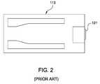
- FIG. 1is a schematic illustration of a disk drive system in which the invention might be embodied
- FIG. 2is an air bearing surface (ABS) view of a slider, taken from line 2 - 2 of FIG. 1 , illustrating the location of a magnetic head thereon;
- ABSair bearing surface
- FIG. 3is a cross sectional view of a magnetic write head according to an embodiment of the present invention.
- FIG. 4Ais a cross sectional view of a pole tip region of a write head according to an alternate embodiment of the invention.
- FIG. 4Bis an air bearing surface (ABS) view of the write head of FIG. 4A , as viewed from line B-B of FIG. 4A ;
- ABSair bearing surface
- FIGS. 5A-5Gillustrate an exemplary method for forming a leading edge shield and leading edge taper for a flared write pole according to an embodiment of the invention
- FIGS. 6A-6Eillustrate one embodiment of a method for forming a leading edge shield according to an embodiment of the invention
- FIGS. 7A-7Eillustrate another embodiment of a method for forming a leading edge shield according to an embodiment of the invention.
- FIGS. 8A-8Fillustrate one embodiment of a method for forming the main pole in addition to the write pole according to an embodiment of the invention.
- Embodiments of the inventionare generally related to leading edge shields and magnetic write heads, and more specifically to methods for fabrication of leading edge shields and tapered magnetic poles.
- a magnetic polemay have a plurality of tapered surfaces at or near an air bearing surface (ABS), wherein a thickness of the write pole increases in a direction away from the ABS.
- ABSair bearing surface
- FIG. 1there is shown a disk drive 100 embodying this invention.
- at least one rotatable magnetic disk 112is supported on a spindle 114 and rotated by a disk drive motor 118 .
- the magnetic recording on each diskis in the form of annular patterns of concentric data tracks (not shown) on the magnetic disk 112 .
- At least one slider 113is positioned near the magnetic disk 112 , each slider 113 supporting one or more magnetic head assemblies 121 . As the magnetic disk rotates, the slider 113 moves radially in and out over the disk surface 122 so that the magnetic head assembly 121 may access different tracks of the magnetic disk where desired data are written.
- Each slider 113is attached to an actuator arm 119 by way of a suspension 115 .
- the suspension 115provides a slight spring force which biases slider 113 against the disk surface 122 .
- Each actuator arm 119is attached to an actuator means 127 .
- the actuator means 127 as shown in FIG. 1may be a voice coil motor (VCM).
- the VCMcomprises a coil movable within a fixed magnetic field, the direction and speed of the coil movements being controlled by the motor current signals supplied by controller 129 .
- the rotation of the magnetic disk 112generates an air bearing between the slider 113 and the disk surface 122 which exerts an upward force or lift on the slider.
- the air bearingthus counter-balances the slight spring force of suspension 115 and supports slider 113 off and slightly above the disk surface by a small, substantially constant spacing during normal operation.
- control unit 129The various components of the disk storage system are controlled in operation by control signals generated by control unit 129 , such as access control signals and internal clock signals.
- control unit 129comprises logic control circuits, storage means and a microprocessor.
- the control unit 129generates control signals to control various system operations such as drive motor control signals on line 123 and head position and seek control signals on line 128 .
- the control signals on line 128provide the desired current profiles to optimally move and position slider 113 to the desired data track on disk 112 .
- Write and read signalsare communicated to and from write and read heads 121 by way of recording channel 125 .
- FIG. 2is an ABS view of the slider 113 , and as can be seen the magnetic head including an inductive write head and a read sensor, is located at a trailing edge of the slider.
- the magnetic head including an inductive write head and a read sensoris located at a trailing edge of the slider.
- FIG. 1The above description of a typical magnetic disk storage system and the accompanying illustration of FIG. 1 are for representation purposes only. It should be apparent that disk storage systems may contain a large number of disks and actuators, and each actuator may support a number of sliders.
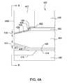
- the inventioncan be embodied in a magnetic head 302 having a tapered write pole and a tapered leading edge.
- a non-magnetic bumpmay also be included in the embodiment as shown in FIG. 3 .
- the magnetic write head 302includes a magnetic write pole 304 and a magnetic return pole 306 .
- a magnetic back gap layer 308 and magnetic shaping layer 310magnetically connect the return pole 306 with the write pole 304 at a location removed from an air bearing surface ABS.
- the magnetic write poleis further defined by a leading edge shield 307 and a leading edge taper 305 .
- An electrically conductive, non-magnetic write coil 318passes between the write pole 304 and the return pole 306 and may also pass above the write pole 304 .
- the write coil 318can sit on top of a non-magnetic, electrically insulating material 322 and is also embedded in a non-magnetic, electrically insulating material 320 such as alumina and/or a hard baked photoresist.
- an electrical current flowing through the coil 318induces a magnetic field the results in a magnetic flux flowing through the write pole 304 .
- This magnetic write fieldflows through the medium to return to the return pole 306 which has a sufficiently large cross section that it does not erase the magnetic bit written by the write pole 304 .
- the write head 302In order to increase the write field gradient (and thereby increase switching speed), the write head 302 also includes a magnetic leading shield 307 having a leading edge taper 305 . Additionally, in order to increase the write field gradient (and thereby increase switching speed), the write head 302 also includes a magnetic trailing shield 312 . This trailing shield 312 is separated from the write pole 304 by a trailing gap layer 332 . The write pole 304 may also be connected with a trailing return pole 316 that connects the trailing shield 312 with the back portion of the write head 302 , such as the back portion of the shaping layer 310 .
- the first width of the write headis between 20 nm and 150 nm and can taper away from the air bearing surface (ABS) at an angle ⁇ with respect to a plane parallel to the ABS surface. In one embodiment ⁇ is between about 30° and about 60°.
- the write head 402includes a write pole 404 that has a tapered trailing edge portion 406 (similar to the previously described embodiment), but which also has a tapered leading edge portion 408 . Having both tapered trailing and leading edges further optimizes the performance of the write head 402 by focusing magnetic flux to the tip of the write pole 404 while avoiding magnetic saturation of the write pole 404 .
- the write head 402has a leading edge shield 410 , a magnetic leading edge shield with a leading edge taper 411 as well as a trailing edge shield 412 , and a trailing magnetic shield.
- the leading edge shield 410is separated from the write pole 404 by a leading gap distance 414
- the trailing edge shield 412is separated from the trailing edge of the write pole 404 by a trailing gap distance 416 , the leading gap distance 414 being significantly larger than the trailing gap distance 416 so as to prevent magnetic write field from being drawn toward the leading edge shield 410 during operation.
- the leading gap distance 414is preferably at least twice the trailing gap distance 416 , and is more preferably about four times the trailing gap distance 416 .
- the leading gap distance 414can be about 100 ⁇ m
- the trailing gap distance 416can be about 25 ⁇ m.
- the leading edge shield 410is separated from the write pole 404 by first and second nonmagnetic layers 418 , 420 .
- the first layer 418can be constructed of a material such as chromium (Cr) or an alloy of nickel-chromium (NiCr).
- the second layer 420can be constructed of a material such as ruthenium (Ru).
- the write headalso includes a non-magnetic spacer layer 422 which can be constructed of a material such as NiCr and can have a thickness of 50-200 ⁇ m.
- the non-magnetic spacer layerhas a front edge 424 that is located a desired distance from the air bearing surface ABS.
- a non-magnetic bump 426constructed of a material such as alumina Al 2 O 3 is formed at the front edge of the non-magnetic spacer layer 422 , extending over a portion of the tapered trailing edge 406 of the write pole 404 .
- the non-magnetic spacer layer 422 and non-magnetic bump layer 426provide additional spacing between the trailing edge shield 412 and the write pole 404 and also optimize the profile of this spacing by providing a smooth transition to this additional spacing.
- the write headalso includes a non-magnetic trailing gap layer 428 that separates the trailing edge shield 412 from the write pole 404 and which may also extend over the non-magnetic bump 426 and non-magnetic spacer layer 422 .
- the nonmagnetic trailing gap layercan be constructed of a material such as Ruthenium.
- non-magnetic, electrically insulating fill layers 430may be provided behind the shields 410 , 412 , although structures could be included in these regions as well.
- a high magnetic moment seed layer 432such as cobalt-iron (CoFe) may be included at the bottom of the trailing edge shield 412 to improve the performance of the trailing shield.
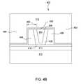
- FIG. 4Bshows the write head 402 as viewed from the air bearing surface.
- the trailing edge shield 412extends downward beyond the sides of the write pole to form side shielding portions 452 , 454 .
- the trailing edge shield 412can also be referred to as a “wrap-around” shield.
- Write headalso includes non-magnetic insulating side fill layers 456 , 458 that (for reasons that will become apparent below) are preferably constructed of a reaction ion etchable (RIEable) material such as SiO 2 or alumina. It also can be seen, that the non-magnetic side fill layers have substantially vertical outer sides, and that the layer 420 discussed above with reference to FIG. 4A , also extends up the sides of the write head (also for reasons that will become apparent below).
- the thickness of the layers 420 , 456 , 428 , 432define the side gap distance 460 .
- the layers 418 and 428extend between the trailing edge shield 412 and the leading edge shield 410 so that the shields 412 , 410 do not contact one another.
- the layers 418 and 428terminate at some point away from the write pole 404 so that the trailing edge shield 412 and leading edge shield 410 make magnetic contact at regions beyond the layers 418 , 428 . This embodiment can improve the performance of the trailing edge shield 412 by improving the flow of magnetic flux from the trailing edge shield 412 .
- FIGS. 5A through 8Gdescribe embodiments of methods for manufacturing a magnetic write head according to the various embodiments described above with reference to FIG. 3 and FIGS. 4A-4B .
- FIGS. 5A-5Gillustrate exemplary steps performed during fabrication of a leading edge taper of a write pole according to an embodiment of the invention.
- fabrication of the structuremay begin by providing a substrate material 500 .
- the substrate material 500may be composed of a non-magnetic material, such as aluminum oxide (Al 2 O 3 ), also known as “alumina”. While not shown in the Figures, the substrate material 500 may include one or more other components of a magnetic head, e.g., a read head and one or more components of a write head already formed therein. Additionally, while not shown, the substrate material 500 may include a reaction ion etchable stop layer ( 310 above) disposed therein to form the bottom of any feature definition. Substrate material 500 may correspond to insulating material 320 of FIG. 3 . In an alternative embodiment, the substrate material 500 may be a magnetic material as described herein.
- the RIE stop layer 510can be a non-magnetic material such as tantalum (Ta), tantalum nitride (TaN), titanium (Ti), titanium nitride (TiN), chromium (Cr), an alloy of nickel and chromium (NiCr), ruthenium (Ru), and combinations thereof, or laminated layers of these materials.
- a fill layer 520is deposited over the material layer 510 .
- the fill layer 520may be a reactive ion etchable (RIEable) material, for example, alumina (Al 2 O 3 ), silicon dioxide (SiO 2 ), silicon nitride, and is deposited at least as thick as the desired thickness of a desired write pole thickness, as will become apparent below.
- RIEablereactive ion etchable
- a feature definition 535may be formed in the reactive ion etchable material (RIEable) of the fill layer 520 by a reactive ion etching (RIE) process, such as ion beam etching (IBE).
- RIEreactive ion etching
- the reactive ion etching (RIE) processis preferably performed at one or more angles relative to normal to form the fill layer 520 with the feature definition 535 having tapered side walls 537 .
- the one or more anglesare from 10° to 60° relative to normal and are angled outward from the bottom of the feature definition to the top of the feature definition.
- Such a structureprovides for a tapered structure from the surface into the material 520 , which can form a trapezoidal shape.
- a non-magnetic material 530which may be a polishing stop material as described in FIGS. 6A-6E , may be deposited by a conformal deposition process such as atomic layer deposition.
- This non-magnetic material 530may be a non-magnetic material including tantalum (Ta), tantalum nitride (TaN), titanium (Ti), titanium nitride (TiN), chromium (Cr), an alloy of nickel and chromium (NiCr), ruthenium (Ru), and combinations thereof, or laminated layers of these materials, and may be deposited to a sufficient thickness to advantageously reduce the width of the trench in order to shrink the track width of the yet to be formed write pole.
- a magnetic material 540such as cobalt-iron (CoFe) or cobalt-nickel-iron (CoNiFe), may be deposited, such as by electroplating, into the feature definition 535 formed in the fill layer 520 .
- the magnetic material 540forms the leading edge shield material of the structure for a later main pole structure.
- a chemical mechanical polishing (CMP) processmay be performed to planarize the magnetic layer 540 , leaving a structure as shown in FIG. 5A , with a write pole material 540 in the feature definition 535 .
- An ion millingmay then also be performed to remove portions of the non-magnetic layer 535 that may extend over the fill layer 520 .
- a magnetic material 550which will be a lead edge taper material, is then conformally deposited, such as by a sputtering process, on the planarized surface of the fill layer 520 , non-magnetic material 530 , and magnetic material 540 .
- the magnetic material 550is a metal alloy selected from the group of nickel-iron (NiFe), cobalt-iron (CoFe), cobalt-nickel-iron (CoNiFe), and combinations thereof.
- the magnetic material 550may the same material or a different material from the magnetic layer 540 .
- the magnetic material 550may be deposited by a sputtering process, and may be deposited to a thickness from about 500 ⁇ to about 1500 ⁇ , for example about 1100 ⁇ .
- a photoresist/resist material 560is then deposited and patterned on the magnetic material 550 .
- an ion milling process or a reactive ion etch processmay be performed to remove portions of the magnetic layer 550 exposed by the patterned photoresist/resist material 560 .
- the ion millingis performed to remove a portion of the magnetic material layer 550 at a preferred angle, thereby allowing the formation of a tapered surface 555 on the magnetic material layer 550 .
- the magnetic layermay be ion milled to provide for the tapered material having the end of the taper portions be within the horizontal surface bounds of the underlying magnetic material 540 as shown in FIG. 5C .
- the magnetic material layer 550has a tapered portions coupled only to the underlying magnetic material 540 on the substrate surface.
- the ion millingis performed at one or more angles relative to normal, such that shadowing from the patterned photoresist/resist layer 560 causes the tapered surface to form an angle from 10 to 60 degrees, such as from 20 to 40 degrees, for example, about 30 degrees with respect to a plane that is parallel with the surfaces of the as deposited layers.
- the tapered structureforms the leading edge taper structure. As shown on the Figures, the leading edge taper may have more than one tapered side, and each side may have the same or substantially the same angles. If any non-magnetic material 550 was disposed on the surface of the layers (not shown), the non-magnetic material 530 may be removed with the ion milling process.
- the patterned photoresist/resist material 560is then removed from the magnetic layer 550 .
- the patterned photoresist/resist material 560may be removed by a liftoff or ashing process.
- a non-magnetic layer 570is conformally deposited over the magnetic material layer 550 and the exposed surfaces of the fill layer 520 , non-magnetic material 530 , and magnetic material 540 .
- the non-magnetic layer 570may be a reactive ion etching (RIE) stop layer and may be a non-magnetic material including tantalum (Ta), tantalum nitride (TaN), titanium (Ti), titanium nitride (TiN), chromium (Cr), an alloy of nickel and chromium (NiCr) ruthenium (Ru), and combinations thereof, or laminated layers of these materials.
- the non-magnetic layer 570may be deposited to a thickness of 40-60 ⁇ m or about 50 ⁇ m.
- a bulk layer 580 of a non-magnetic materialsuch as alumina, may be deposited over the conformal non-magnetic RIE stop layer 570 .
- the bulk layer 580(and optionally, the non-magnetic RIE stop layer 570 ) may then be planarized.
- the substrate material 500 and bulk layer 580may be of the same material, and may comprises a material selected from the group of alumina (Al 2 O 3 ), silicon oxide, silicon nitride, an combinations thereof, amongst other dielectric materials.
- the formed structuremay then provide for main pole processing.
- FIG. 5Gillustrates the layering structure after the air bearing surface process which shows the leading edge shield portion 340 and the leading edge taper portion 355 containing the ABS allowing for the formation of the write pole with a leading tapered surface as shown in FIG. 3 .
- FIG. 5Amay be formed by several different processes, of which two embodiments can be described as follows with reference to FIGS. 6A-6E and FIGS. 7A-7E , respectively.
- One manner to form the leading edge shieldcomprises depositing a seed layer over a substrate.
- the seed layermay be deposited by conventional deposition techniques such as electroplating or sputtering.
- a photoresist maskis then formed which leaves select areas of the seed layer exposed.
- the magnetic materialis then deposited onto the exposed areas of the seed layer.
- the maskmay then be removed, as well as the exposed seed layer that underlies the mask. The removal may occur utilizing ion beam milling to expose the underlying substrate.
- a layer of Al 2 O 3may then be formed over the exposed surfaces which include portions of the substrate and the magnetic material.
- the Al 2 O 3may then be planarized back using a CMP process to expose the magnetic material, which is also polished at least partially.
- the process flowis simple, but can not achieve the desired uniformity for the preferred 0.1 to 0.3 micron thickness of the leading edge shield and hence, has no manufacturability.
- the process flow discussed below in regards to FIGS. 6A-6Eincludes depositing a CMP stop layer, photo pattern, etch, refill, CMP and light mill to provide a better leading edge shield thickness mean and uniformity control.
- the process flow discussed below in regards to FIGS. 7A-7Einvolves etching, refilling with a stop layer and leading edge shield material, then CMP and light ion beam etching.
- the process flow for FIGS. 6A-6Ewill leave no process signature of the CMP stop layer while the process flow for FIGS. 7A-7E will have the process signature of a CMP stop layer.
- the leading edge shieldfor both FIGS. 6A-6E and FIGS. 7A-7E are fabricated after the reader is completed.
- the leading edge shieldis fabricated with a throat height length ranging from about 0.2 microns to about 0.3 microns.
- the thickness of the leading edge shieldis between about 0.1 microns and about 0.3 microns.
- the magnetic material for the leading edge shieldmay comprise soft magnetic materials such as NiFe, CoNiFe, and CoFe.
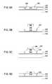
- the structure of FIG. 5Amay be formed by first providing a substrate material 600 .
- the substrate material 600may be composed of a non-magnetic material, such as aluminum oxide (Al 2 O 3 ), also know as “alumina”. While not shown in the Figures, the substrate material 600 may include one or more other components of a magnetic head, e.g., a read head and one or more components of a write head already formed therein. Additionally, while not shown, the substrate material 600 may include a reaction ion etchable layer stop layer ( 310 above) disposed therein to form the bottom of any feature definition. Substrate material 600 may correspond to insulating material 320 of FIG. 3 . In an alternative embodiment, the substrate material 600 may be a magnetic material as described herein.
- the CMP resistance material 610may be a material selected from the group consisting of iridium (Ir), ruthenium (Ru), Rhodium (Rh), tantalum (Ta), and combinations thereof, and is preferably a non-magnetic material.
- the CMP resistance material 610may be deposited to a thickness from 100 ⁇ to 500 ⁇ .
- a photoresist material 620is then deposited and patterned on the CMP resistance material 610 .
- a feature definition 625may be formed in the substrate material 600 by reactive ion etching (RIE) or ion beam etching (IBE) the exposed CMP resistance material 610 and the underlying substrate material 600 .
- the reactive ion etch processis preferably performed at one or more angles relative to normal to form the feature definition 625 having tapered side walls 627 .
- the one or more anglesare from 10° to 60° relative to normal and are angled outward from the bottom of the feature definition to the top of the feature definition.
- the photoresist/resist material 620is also removed after the etching process, such as by a liftoff or ashing process.
- the feature definitionis formed having a depth (or thickness) from 0.1 ⁇ m to 0.3 ⁇ m.
- a magnetic material 630such as cobalt-iron (CoFe) of cobalt-nickel-iron (CoNiFe), may be deposited on the CMP stop layer 610 and into the feature definition 625 formed in the substrate material 600 as shown in FIG. 6C .
- the magnetic material 630may be deposited by a plating process, such as electroplating, or a physical vapor deposition (sputtering) process.
- a planarization processsuch as by a chemical mechanical polishing (CMP) process, may be performed to remove the magnetic layer 630 deposited over the CMP stop layer 610 and planarize the magnetic layer 630 to the CMP resistance material 610 , leaving a structure shown in FIG. 6D , which is in essence a leading edge shield formed in the feature definition 625 .
- CMPchemical mechanical polishing
- An ion millingsuch as by a light ion beam etching process (IBE) or sputter etching process may then also be performed to remove portions of the CMP resistance material 610 still remaining after the planarization process as shown in FIG. 6E .
- the ion millingcan be skipped if a LET process is used further down the line.
- the ion millingmay remove between about 100 Angstroms and about 500 Angstroms.
- the structuremay be formed by first providing a substrate material 700 .
- the substrate material 700may be composed of a non-magnetic material, such as Aluminum Oxide (Al 2 O 3 ), also know as “alumina”. While not shown in the figures, the substrate material 700 may include one or more other components of a magnetic head, e.g., a read head and one or more components of a write head already formed therein.
- a photoresist/resist material 720is then deposited and patterned on the substrate material 700 . Additionally, while not shown, the substrate material 700 may include a reaction ion etchable layer stop layer ( 310 above) disposed therein to form the bottom of any feature definition.
- Substrate material 700may correspond to insulating material 320 of FIG. 3 .
- the substrate material 700may be a magnetic material as described herein.
- a feature definition 725may be formed in the substrate material 700 by reactive ion etching (RIE) or ion beam etching (IBM) the exposed substrate material 700 .
- the reactive ion etch processis preferably performed at one or more angles relative to normal to form the feature definition 725 having tapered side walls 727 .
- the one or more anglesare from 10° to 60° relative to normal and are angled outward from the bottom of the feature definition 725 to the top of the feature definition 725 .
- the feature definition 725is formed having a depth (or thickness) from 0.1 ⁇ m to 0.3 ⁇ m.
- the photoresist/resist material 720is also removed after the etching process, such as by a liftoff or ashing process.
- the CMP resistance material 710may be a material selected from the group consisting of iridium (Ir), ruthenium (Ru), Rhodium (Rh), tantalum (Ta), and combinations thereof, and is preferably a non-magnetic material.
- the CMP resistance material 710may be sputter deposited to a thickness from 100 ⁇ to 500 ⁇ .
- a magnetic material 730such as cobalt-iron (CoFe) or cobalt-nickel-iron (CoNiFe), may be deposited onto the CMP resistance material 710 and into the feature definition 725 formed in the substrate material 700 as shown in FIG. 7C .
- the magnetic material 730may be deposited by a plating process, such as electroplating, or a physical vapor deposition (sputtering) process.
- a planarization processsuch as by a chemical mechanical polishing (CMP) process, may be performed to remove and planarize the magnetic layer 730 to the CMP resistance material 710 , leaving a structure shown in FIG. 7D , which is in essence a leading edge shield formed in the feature definition 725 .
- CMPchemical mechanical polishing
- An ion millingsuch as by a light ion beam etching process (IBE) may then also be performed to remove portions of the CMP resistance material 710 still remaining after the planarization process as shown in FIG. 7E .
- IBElight ion beam etching process
- FIGS. 6A-6E and 7 A- 7 Eare comparable.
- the process flow in FIGS. 6A-6Ewill leave no process signature of a CMP stop layer while the process flow in FIGS. 7A-7E will have a process signature of a CMP stop layer.
- a Cr/NiCr RIE stop layermay be deposited on the leading edge shield after the leading edge shield is completed to make a perpendicular write head with a four side wrap-around shield but without the leading edge taper. After the leading edge shield is done, the leading edge taper can also be built upon the leading edge shield so that the perpendicular write head will have both a leading edge shield and a leading edge taper.
- one embodiment of forming a main pole on the write materialis as follows.
- the non-magnetic fill material 380 as shown in FIG. 5Fis removed.
- An optional non-magnetic step layer, preferably constructed of NiCrmay be deposited over the non-magnetic layer 570 (non-magnetic reactive ion etching (RIE) stop layer) and the leading edge taper material 555 .
- the pole material 810may then be deposited and planarized.
- the pole material 810may comprise a magnetic material as described herein.
- a non-magnetic step layer 820preferably constructed of NiCr is deposited over the pole material 810 .
- a mask layer and/or a photoresist/resist layer(not shown) are deposited and patterned over the non-magnetic step layer 820 and the pole material 810 .
- the non-magnetic step layer 820 and the pole material 810are then etched and patterned by an ion milling process to form an upper tapered surface 825 . Any mask or photoresist/resist material are then removed to provide the structure as shown in FIG. 8B .
- a layer of non-magnetic material 830is deposited by a conformal deposition process such as atomic layer deposition or chemical vapor deposition as shown in FIG. 8C .
- a layer of non-magnetic material 840is deposited to a thickness to define a desired trailing gap thickness as shown in FIG. 8D .
- the trailing gap layer 840can be constructed of ruthenium and other non-magnetic materials.
- a non-magnetic, electrically insulating material 860such as alumina 860 , may then be deposited on the trailing gap layer 840 .
- the non-magnetic, electrically insulating material 860may then be etched to expose a portion of the trailing gap layer 840 formed from the air bearing surface to a portion along the substantially horizontal portion of the trailing gap layer 840 .
- An optional high magnetic moment seed layer 850may be deposited and patterned on the exposed trailing gap layer 840 .
- a trailing shield 870may be deposited on the high magnetic seed layer 850 .
- the high magnetic moment seed layer 850may be provided at the leading edge of the trailing shield 870 ( 312 ) to maximize the performance of the trailing shield.
- Additional structuressuch as a trailing return pole, additional non-magnetic, electrically insulating material, and coils may be formed on the structure to form the head structure.
- the structuremay then be processed to form an air bearing surface, as shown by line ABS formed through the structure in FIG. 8F to form the structure as shown in FIG. 3 .
Landscapes
- Engineering & Computer Science (AREA)
- Manufacturing & Machinery (AREA)
- Physics & Mathematics (AREA)
- Electromagnetism (AREA)
- Magnetic Heads (AREA)
Abstract
Description
Claims (20)
Priority Applications (2)
| Application Number | Priority Date | Filing Date | Title |
|---|---|---|---|
| US12/954,485US8524095B2 (en) | 2010-11-24 | 2010-11-24 | Process to make PMR writer with leading edge shield (LES) and leading edge taper (LET) |
| JP2011246127AJP2012113806A (en) | 2010-11-24 | 2011-11-10 | Process to make pmr writer with leading edge shield (les) and leading edge taper (let) |
Applications Claiming Priority (1)
| Application Number | Priority Date | Filing Date | Title |
|---|---|---|---|
| US12/954,485US8524095B2 (en) | 2010-11-24 | 2010-11-24 | Process to make PMR writer with leading edge shield (LES) and leading edge taper (LET) |
Publications (2)
| Publication Number | Publication Date |
|---|---|
| US20120125886A1 US20120125886A1 (en) | 2012-05-24 |
| US8524095B2true US8524095B2 (en) | 2013-09-03 |
Family
ID=46063348
Family Applications (1)
| Application Number | Title | Priority Date | Filing Date |
|---|---|---|---|
| US12/954,485Expired - Fee RelatedUS8524095B2 (en) | 2010-11-24 | 2010-11-24 | Process to make PMR writer with leading edge shield (LES) and leading edge taper (LET) |
Country Status (2)
| Country | Link |
|---|---|
| US (1) | US8524095B2 (en) |
| JP (1) | JP2012113806A (en) |
Cited By (4)
| Publication number | Priority date | Publication date | Assignee | Title |
|---|---|---|---|---|
| US9153253B2 (en)* | 2014-01-08 | 2015-10-06 | Tdk Corporation | Perpendicular magnetic recording head and magnetic recording unit having leading shield including exposed end surface and recess shield including mid part |
| US9478242B1 (en) | 2016-03-25 | 2016-10-25 | Western Digital (Fremont), Llc | Magnetic recording apparatus having a recessed additional pole segment |
| US11651783B1 (en)* | 2022-02-22 | 2023-05-16 | Western Digital Technologies, Inc. | Two layer leading shield design with non-conformal shapes for magnetic recording heads |
| US11881235B2 (en) | 2022-02-22 | 2024-01-23 | Western Digital Technologies, Inc. | Leading shield for magnetic recording heads |
Families Citing this family (8)
| Publication number | Priority date | Publication date | Assignee | Title |
|---|---|---|---|---|
| US8576514B2 (en)* | 2011-12-16 | 2013-11-05 | Headway Technologies, Inc. | Thin-film magnetic head, method of manufacturing the same, head gimbal assembly, and hard disk drive |
| US8451563B1 (en)* | 2011-12-20 | 2013-05-28 | Western Digital (Fremont), Llc | Method for providing a side shield for a magnetic recording transducer using an air bridge |
| US8498079B1 (en)* | 2012-09-15 | 2013-07-30 | Headway Technologies, Inc. | Superior performance head design with minimized ATE and WATE |
| US8980109B1 (en) | 2012-12-11 | 2015-03-17 | Western Digital (Fremont), Llc | Method for providing a magnetic recording transducer using a combined main pole and side shield CMP for a wraparound shield scheme |
| US9548069B2 (en)* | 2013-03-14 | 2017-01-17 | HGST Netherlands B.V. | Method for producing a smooth Ru side gap of a damascene writer pole |
| US9318131B2 (en)* | 2013-06-28 | 2016-04-19 | Seagate Technology Llc | Write gap structure for a magnetic recording head |
| US10741202B2 (en)* | 2017-10-05 | 2020-08-11 | Western Digital Technologies, Inc. | MAMR writer with low resistance MAMR stack |
| US10339964B1 (en)* | 2018-05-21 | 2019-07-02 | Headway Technologies, Inc. | Perpendicular magnetic recording (PMR) write head with patterned high moment trailing shield |
Citations (48)
| Publication number | Priority date | Publication date | Assignee | Title |
|---|---|---|---|---|
| US6501619B1 (en) | 2000-04-27 | 2002-12-31 | Shipley Company, L.L.C. | Inductive magnetic recording head having inclined magnetic read/write pole and method of making same |
| US6989972B1 (en) | 2002-09-30 | 2006-01-24 | Western Digital (Fremont), Inc. | Magnetoresistive sensor with overlapping leads having distributed current |
| US7038882B2 (en) | 2002-10-03 | 2006-05-02 | Seagate Technology | Low moment-high moment write pole with non-magnetic layer for establishing a magnetic path discontinuity between layers of the write pole |
| JP2006147023A (en) | 2004-11-18 | 2006-06-08 | Fujitsu Ltd | Thin film magnetic head and manufacturing method thereof |
| US7075756B1 (en) | 2002-11-07 | 2006-07-11 | Maxtor Corporation | Shielded pole writer |
| US20060187581A1 (en) | 2005-02-24 | 2006-08-24 | Fujitsu Limited | Magnetic head and method of manufacturing the same |
| US7140095B2 (en) | 2003-03-31 | 2006-11-28 | Sae Magnetics (H.K.) Ltd. | Method of manufacturing a thin film magnetic head |
| US20060279882A1 (en) | 2005-06-14 | 2006-12-14 | Kenji Honda | Magnetic detecting element having rie-resistant film and method of manufacturing the same |
| US7159302B2 (en) | 2004-03-31 | 2007-01-09 | Hitachi Global Storage Technologies Netherlands B.V. | Method for manufacturing a perpendicular write head |
| US7251878B2 (en) | 2004-06-30 | 2007-08-07 | Hitachi Global Storage Technologies Netherlands B.V. | Method and apparatus for defining leading edge taper of a write pole tip |
| US7253992B2 (en) | 2004-11-04 | 2007-08-07 | Hitachi Global Storage Technologies Netherlands, B.V. | Single-pole recording head having trapezoidal main pole and bevel angle promotion layer and methods of fabricating the same |
| US20070217069A1 (en) | 2006-03-15 | 2007-09-20 | Hitachi Global Storage Technologies Netherlands B.V. | Perpendicular magnetic recording head and method of manufacturing the same |
| US20070253117A1 (en) | 2006-04-17 | 2007-11-01 | Hitachi Global Storage Technologies Inc. | Magnetic head and method for fabricating the same |
| US20080112081A1 (en) | 2006-11-10 | 2008-05-15 | Sae Magnetics (H.K.) Ltd. | Perpendicular magnetic write head, method of manufacturing the same, and magnetic recording apparatus |
| US7375925B2 (en) | 2005-05-27 | 2008-05-20 | Headway Technologies, Inc. | Magnetic head for perpendicular magnetic recording and method of manufacturing same |
| US7392577B2 (en) | 2003-09-12 | 2008-07-01 | Tdk Corporation | Method for manufacturing a perpendicular magnetic head |
| US20080155810A1 (en) | 2006-12-27 | 2008-07-03 | Ying Hong | Methods for fabricating a magnetic sensor head using a cmp defined hard bias and a totally flat reader gap |
| US7417824B2 (en) | 2004-11-10 | 2008-08-26 | Tdk Corporation | Perpendicular magnetic recording head where main magnetic pole having inclined surface is formed and method of manufacturing the same |
| US20080239585A1 (en) | 2007-01-04 | 2008-10-02 | Hitachi Global Storage Technologies Netherlands B.V. | CPP-type magnetoresistive effect head and method of manufacturing the same |
| US20080239567A1 (en) | 2007-03-26 | 2008-10-02 | Headway Technologies, Inc. | Magnetic head for perpendicular magnetic recording and method of manufacturing same |
| US20080253035A1 (en)* | 2007-03-27 | 2008-10-16 | Headway Technologies, Inc. | Self-aligned full side shield PMR and method to make it |
| US20080259498A1 (en) | 2007-04-19 | 2008-10-23 | Hitachi Global Storage Technologies | Perpendicular write head with independent trailing shield designs |
| US20080266724A1 (en) | 2007-04-25 | 2008-10-30 | Tdk Corporation | Perpendicular magnetic recording head |
| US20080266710A1 (en) | 2007-04-25 | 2008-10-30 | Tdk Corporation | Perpendicular magnetic recording head |
| US20080278862A1 (en) | 2007-05-08 | 2008-11-13 | Tdk Corporation | Perpendicular magnetic recording head |
| US20080278853A1 (en) | 2007-05-08 | 2008-11-13 | Tdk Corporation | Perpendicular magnetic recording head |
| US20080278861A1 (en) | 2007-05-11 | 2008-11-13 | Ming Jiang | Stitched wrap around shield fabrication for perpendicular magnetic recording write heads |
| US20090002885A1 (en) | 2007-06-28 | 2009-01-01 | Samsung Electronics Co., Ltd. | Perpendicular magnetic recording head and method of manufacturing the same |
| JP2009048719A (en) | 2007-08-21 | 2009-03-05 | Hitachi Global Storage Technologies Netherlands Bv | Magnetic head and magnetic recording apparatus |
| US20090091862A1 (en)* | 2007-10-03 | 2009-04-09 | Headway Technologies, Inc. | Method to make PMR head with integrated side shield (ISS) |
| US20090122445A1 (en) | 2007-11-13 | 2009-05-14 | Hitachi Global Storage Technologies Netherlands B.V. | Perpendicular magnetic recording write head with flux shaping layers on the write pole and magnetic recording system incorporating the write head |
| US20090141406A1 (en) | 2007-12-04 | 2009-06-04 | Headway Technologies, Inc. | Magnetic head for perpendicular magnetic recording and method of manufacturing same |
| US20090147410A1 (en) | 2007-12-06 | 2009-06-11 | Hitachi Global Storage Technologies Netherlands B.V. | Perpendicular magnetic recording write head with magnetic shields separated by nonmagnetic layers |
| US20090154019A1 (en) | 2007-12-17 | 2009-06-18 | Hitachi Global Storage Technologies Netherlands B.V. | Perpendicular magnetic recording write head with slanted magnetic write pole |
| US20090152119A1 (en) | 2007-12-14 | 2009-06-18 | Fujitsu Limited | Method for manufacturing magnetic head |
| US7561384B2 (en) | 2004-12-21 | 2009-07-14 | Hitachi Global Storage Technologies Netherlands B.V. | Magneto-resistive sensor having small track width and sensor height using stopper layer |
| JP2009187612A (en) | 2008-02-05 | 2009-08-20 | Fujitsu Ltd | Manufacturing method of magnetic head |
| US20090244789A1 (en) | 2008-04-01 | 2009-10-01 | Westem Digital (Fremont), Llc | Method and system for providing a hard bias capping layer |
| JP2009224000A (en) | 2008-03-18 | 2009-10-01 | Fujitsu Ltd | Method of manufacturing magnetic head |
| JP2009238261A (en) | 2008-03-26 | 2009-10-15 | Fujitsu Ltd | Reproduction magnetic head and manufacturing method thereof |
| US20090266790A1 (en) | 2008-04-28 | 2009-10-29 | Hamid Balamane | Method of making a magnetoresistive reader structure |
| US20090277870A1 (en)* | 2008-05-12 | 2009-11-12 | Headway Technologies, Inc. | Method of manufacturing magnetic head for perpendicular magnetic recording |
| US20090283205A1 (en) | 2008-05-16 | 2009-11-19 | Fujitsu Limited | Method of manufacturing a thin-film magnetic head |
| US7623324B2 (en) | 2005-06-22 | 2009-11-24 | Tdk Corporation | Magnetic sensing element having reactive-ion-etching stop layer and process for producing same |
| US20100024201A1 (en) | 2008-07-31 | 2010-02-04 | Quang Le | Method for fabricating narrow magnetic read width tmr/cpp sensors |
| JP2010033621A (en) | 2008-07-24 | 2010-02-12 | Fujitsu Ltd | Magnetic head, manufacturing method therefor, and magnetic storage device |
| JP2010061735A (en) | 2008-09-03 | 2010-03-18 | Fujitsu Ltd | Magnetic head and method for manufacturing the same and information storage device |
| US20100315741A1 (en)* | 2009-06-12 | 2010-12-16 | Sae Magnetics (H.K.) Ltd. | Perpendicular magnetic recording head |
- 2010
- 2010-11-24USUS12/954,485patent/US8524095B2/ennot_activeExpired - Fee Related
- 2011
- 2011-11-10JPJP2011246127Apatent/JP2012113806A/enactivePending
Patent Citations (50)
| Publication number | Priority date | Publication date | Assignee | Title |
|---|---|---|---|---|
| US6501619B1 (en) | 2000-04-27 | 2002-12-31 | Shipley Company, L.L.C. | Inductive magnetic recording head having inclined magnetic read/write pole and method of making same |
| US6989972B1 (en) | 2002-09-30 | 2006-01-24 | Western Digital (Fremont), Inc. | Magnetoresistive sensor with overlapping leads having distributed current |
| US7038882B2 (en) | 2002-10-03 | 2006-05-02 | Seagate Technology | Low moment-high moment write pole with non-magnetic layer for establishing a magnetic path discontinuity between layers of the write pole |
| US7075756B1 (en) | 2002-11-07 | 2006-07-11 | Maxtor Corporation | Shielded pole writer |
| US7140095B2 (en) | 2003-03-31 | 2006-11-28 | Sae Magnetics (H.K.) Ltd. | Method of manufacturing a thin film magnetic head |
| US7392577B2 (en) | 2003-09-12 | 2008-07-01 | Tdk Corporation | Method for manufacturing a perpendicular magnetic head |
| US7159302B2 (en) | 2004-03-31 | 2007-01-09 | Hitachi Global Storage Technologies Netherlands B.V. | Method for manufacturing a perpendicular write head |
| US7251878B2 (en) | 2004-06-30 | 2007-08-07 | Hitachi Global Storage Technologies Netherlands B.V. | Method and apparatus for defining leading edge taper of a write pole tip |
| US7253992B2 (en) | 2004-11-04 | 2007-08-07 | Hitachi Global Storage Technologies Netherlands, B.V. | Single-pole recording head having trapezoidal main pole and bevel angle promotion layer and methods of fabricating the same |
| US7417824B2 (en) | 2004-11-10 | 2008-08-26 | Tdk Corporation | Perpendicular magnetic recording head where main magnetic pole having inclined surface is formed and method of manufacturing the same |
| JP2006147023A (en) | 2004-11-18 | 2006-06-08 | Fujitsu Ltd | Thin film magnetic head and manufacturing method thereof |
| US7561384B2 (en) | 2004-12-21 | 2009-07-14 | Hitachi Global Storage Technologies Netherlands B.V. | Magneto-resistive sensor having small track width and sensor height using stopper layer |
| US20060187581A1 (en) | 2005-02-24 | 2006-08-24 | Fujitsu Limited | Magnetic head and method of manufacturing the same |
| US7375925B2 (en) | 2005-05-27 | 2008-05-20 | Headway Technologies, Inc. | Magnetic head for perpendicular magnetic recording and method of manufacturing same |
| US20060279882A1 (en) | 2005-06-14 | 2006-12-14 | Kenji Honda | Magnetic detecting element having rie-resistant film and method of manufacturing the same |
| US7623324B2 (en) | 2005-06-22 | 2009-11-24 | Tdk Corporation | Magnetic sensing element having reactive-ion-etching stop layer and process for producing same |
| US20070217069A1 (en) | 2006-03-15 | 2007-09-20 | Hitachi Global Storage Technologies Netherlands B.V. | Perpendicular magnetic recording head and method of manufacturing the same |
| US20070253117A1 (en) | 2006-04-17 | 2007-11-01 | Hitachi Global Storage Technologies Inc. | Magnetic head and method for fabricating the same |
| US20080112081A1 (en) | 2006-11-10 | 2008-05-15 | Sae Magnetics (H.K.) Ltd. | Perpendicular magnetic write head, method of manufacturing the same, and magnetic recording apparatus |
| US20080155810A1 (en) | 2006-12-27 | 2008-07-03 | Ying Hong | Methods for fabricating a magnetic sensor head using a cmp defined hard bias and a totally flat reader gap |
| US20080239585A1 (en) | 2007-01-04 | 2008-10-02 | Hitachi Global Storage Technologies Netherlands B.V. | CPP-type magnetoresistive effect head and method of manufacturing the same |
| US20080239567A1 (en) | 2007-03-26 | 2008-10-02 | Headway Technologies, Inc. | Magnetic head for perpendicular magnetic recording and method of manufacturing same |
| US20080253035A1 (en)* | 2007-03-27 | 2008-10-16 | Headway Technologies, Inc. | Self-aligned full side shield PMR and method to make it |
| US7979978B2 (en)* | 2007-03-27 | 2011-07-19 | Headway Technologies, Inc. | Method for manufacturing a self-aligned full side shield PMR |
| US20080259498A1 (en) | 2007-04-19 | 2008-10-23 | Hitachi Global Storage Technologies | Perpendicular write head with independent trailing shield designs |
| US20080266724A1 (en) | 2007-04-25 | 2008-10-30 | Tdk Corporation | Perpendicular magnetic recording head |
| US20080266710A1 (en) | 2007-04-25 | 2008-10-30 | Tdk Corporation | Perpendicular magnetic recording head |
| US20080278862A1 (en) | 2007-05-08 | 2008-11-13 | Tdk Corporation | Perpendicular magnetic recording head |
| US20080278853A1 (en) | 2007-05-08 | 2008-11-13 | Tdk Corporation | Perpendicular magnetic recording head |
| US20080278861A1 (en) | 2007-05-11 | 2008-11-13 | Ming Jiang | Stitched wrap around shield fabrication for perpendicular magnetic recording write heads |
| US20090002885A1 (en) | 2007-06-28 | 2009-01-01 | Samsung Electronics Co., Ltd. | Perpendicular magnetic recording head and method of manufacturing the same |
| JP2009048719A (en) | 2007-08-21 | 2009-03-05 | Hitachi Global Storage Technologies Netherlands Bv | Magnetic head and magnetic recording apparatus |
| US20090091862A1 (en)* | 2007-10-03 | 2009-04-09 | Headway Technologies, Inc. | Method to make PMR head with integrated side shield (ISS) |
| US20090122445A1 (en) | 2007-11-13 | 2009-05-14 | Hitachi Global Storage Technologies Netherlands B.V. | Perpendicular magnetic recording write head with flux shaping layers on the write pole and magnetic recording system incorporating the write head |
| US20090141406A1 (en) | 2007-12-04 | 2009-06-04 | Headway Technologies, Inc. | Magnetic head for perpendicular magnetic recording and method of manufacturing same |
| US20090147410A1 (en) | 2007-12-06 | 2009-06-11 | Hitachi Global Storage Technologies Netherlands B.V. | Perpendicular magnetic recording write head with magnetic shields separated by nonmagnetic layers |
| US20090152119A1 (en) | 2007-12-14 | 2009-06-18 | Fujitsu Limited | Method for manufacturing magnetic head |
| US20090154019A1 (en) | 2007-12-17 | 2009-06-18 | Hitachi Global Storage Technologies Netherlands B.V. | Perpendicular magnetic recording write head with slanted magnetic write pole |
| JP2009187612A (en) | 2008-02-05 | 2009-08-20 | Fujitsu Ltd | Manufacturing method of magnetic head |
| JP2009199712A (en) | 2008-02-25 | 2009-09-03 | Headway Technologies Inc | Vertical magnetic recording head and its manufacturing method |
| JP2009224000A (en) | 2008-03-18 | 2009-10-01 | Fujitsu Ltd | Method of manufacturing magnetic head |
| JP2009238261A (en) | 2008-03-26 | 2009-10-15 | Fujitsu Ltd | Reproduction magnetic head and manufacturing method thereof |
| US20090244789A1 (en) | 2008-04-01 | 2009-10-01 | Westem Digital (Fremont), Llc | Method and system for providing a hard bias capping layer |
| US20090266790A1 (en) | 2008-04-28 | 2009-10-29 | Hamid Balamane | Method of making a magnetoresistive reader structure |
| US20090277870A1 (en)* | 2008-05-12 | 2009-11-12 | Headway Technologies, Inc. | Method of manufacturing magnetic head for perpendicular magnetic recording |
| US20090283205A1 (en) | 2008-05-16 | 2009-11-19 | Fujitsu Limited | Method of manufacturing a thin-film magnetic head |
| JP2010033621A (en) | 2008-07-24 | 2010-02-12 | Fujitsu Ltd | Magnetic head, manufacturing method therefor, and magnetic storage device |
| US20100024201A1 (en) | 2008-07-31 | 2010-02-04 | Quang Le | Method for fabricating narrow magnetic read width tmr/cpp sensors |
| JP2010061735A (en) | 2008-09-03 | 2010-03-18 | Fujitsu Ltd | Magnetic head and method for manufacturing the same and information storage device |
| US20100315741A1 (en)* | 2009-06-12 | 2010-12-16 | Sae Magnetics (H.K.) Ltd. | Perpendicular magnetic recording head |
Cited By (4)
| Publication number | Priority date | Publication date | Assignee | Title |
|---|---|---|---|---|
| US9153253B2 (en)* | 2014-01-08 | 2015-10-06 | Tdk Corporation | Perpendicular magnetic recording head and magnetic recording unit having leading shield including exposed end surface and recess shield including mid part |
| US9478242B1 (en) | 2016-03-25 | 2016-10-25 | Western Digital (Fremont), Llc | Magnetic recording apparatus having a recessed additional pole segment |
| US11651783B1 (en)* | 2022-02-22 | 2023-05-16 | Western Digital Technologies, Inc. | Two layer leading shield design with non-conformal shapes for magnetic recording heads |
| US11881235B2 (en) | 2022-02-22 | 2024-01-23 | Western Digital Technologies, Inc. | Leading shield for magnetic recording heads |
Also Published As
| Publication number | Publication date |
|---|---|
| JP2012113806A (en) | 2012-06-14 |
| US20120125886A1 (en) | 2012-05-24 |
Similar Documents
| Publication | Publication Date | Title |
|---|---|---|
| US8400733B2 (en) | Process to make PMR writer with leading edge shield (LES) and leading edge taper (LET) | |
| US8524095B2 (en) | Process to make PMR writer with leading edge shield (LES) and leading edge taper (LET) | |
| US8547660B2 (en) | Magnetic write head manufactured by an enhanced damascene process producing a tapered write pole with a non-magnetic spacer and non-magnetic bump | |
| US8201320B2 (en) | Method for manufacturing a magnetic write head having a wrap around shield that is magnetically coupled with a leading magnetic shield | |
| US8470186B2 (en) | Perpendicular write head with wrap around shield and conformal side gap | |
| US8347488B2 (en) | Magnetic write head manufactured by damascene process producing a tapered write pole with a non-magnetic step and non-magnetic bump | |
| US8441757B2 (en) | Perpendicular magnetic write head with wrap-around shield, slanted pole and slanted pole bump fabricated by damascene process | |
| US8347489B2 (en) | Method for manufacturing a perpendicular magnetic write head having a leading edge tapered write pole, self aligned side shield and independent trailing shield | |
| US8323727B2 (en) | Method for manufacturing a perpendicular magnetic write head having a tapered write pole and a stepped wrap around side shield gap | |
| US7612963B2 (en) | Perpendicular magnetic recording head with photoresist dam between write coil and air bearing surface | |
| US8066892B2 (en) | Method for manufacturing a perpendicular magnetic write head with a wrap around shield | |
| US7963024B2 (en) | Method of manufacturing a magnetic write head for perpendicular magnetic recording | |
| US9047894B2 (en) | Magnetic write head having spin torque oscillator that is self aligned with write pole | |
| US8110085B2 (en) | Assisted deposition, narrow trench damascene process for manufacturing a write pole of a magnetic write head | |
| US8339734B2 (en) | Magnetic write head having a wrap around trailing shield with an asymetrical side gap | |
| US8451562B2 (en) | Method for manufacturing a magnetic write head having a wrap around trailing magnetic shield with a tapered side gap | |
| US8268407B2 (en) | Method for manufacturing a perpendicular magnetic write head having write pole | |
| US7788798B2 (en) | Method for manufacturing a perpendicular magnetic write head with wrap around magnetic trailing and side shields | |
| US7881010B2 (en) | Process for self-aligned flare point and shield throat definition prior to main pole patterning | |
| US20120154951A1 (en) | Method for manufacturing a perpendicular magnetic write pole having a write pole and trailing shield with a tapered trailing gap | |
| US8349197B2 (en) | Method for manufacturing a perpendicular magnetic write head having a tapered write pole and non-magnetic bump structure | |
| US8371019B1 (en) | Method for manufacturing a magnetic write pole having straight side walls and a well defined track-width | |
| US8318031B2 (en) | Method for manufacturing a perpendicular magnetic write head having a tapered write pole | |
| US8252190B2 (en) | Method for manufacturing a magnetic write head having a hard mask defined write pole trailing edge step | |
| US20120231296A1 (en) | Method for manufacturing an advanced magnetic read sensor |
Legal Events
| Date | Code | Title | Description |
|---|---|---|---|
| AS | Assignment | Owner name:HITACHI GLOBAL STORAGE TECHNOLOGIES NETHERLANDS B. Free format text:ASSIGNMENT OF ASSIGNORS INTEREST;ASSIGNORS:HONG, LIUBO;LIU, FENGLIN;ZHONG, QIPING;AND OTHERS;SIGNING DATES FROM 20100825 TO 20100826;REEL/FRAME:025449/0142 | |
| AS | Assignment | Owner name:HGST, NETHERLANDS B.V., NETHERLANDS Free format text:CHANGE OF NAME;ASSIGNOR:HGST, NETHERLANDS B.V.;REEL/FRAME:029341/0777 Effective date:20120723 Owner name:HGST NETHERLANDS B.V., NETHERLANDS Free format text:CHANGE OF NAME;ASSIGNOR:HITACHI GLOBAL STORAGE TECHNOLOGIES NETHERLANDS B.V.;REEL/FRAME:029341/0777 Effective date:20120723 | |
| FEPP | Fee payment procedure | Free format text:PAYOR NUMBER ASSIGNED (ORIGINAL EVENT CODE: ASPN); ENTITY STATUS OF PATENT OWNER: LARGE ENTITY | |
| AS | Assignment | Owner name:WESTERN DIGITAL TECHNOLOGIES, INC., CALIFORNIA Free format text:ASSIGNMENT OF ASSIGNORS INTEREST;ASSIGNOR:HGST NETHERLANDS B.V.;REEL/FRAME:040826/0327 Effective date:20160831 | |
| REMI | Maintenance fee reminder mailed | ||
| LAPS | Lapse for failure to pay maintenance fees | Free format text:PATENT EXPIRED FOR FAILURE TO PAY MAINTENANCE FEES (ORIGINAL EVENT CODE: EXP.) | |
| STCH | Information on status: patent discontinuation | Free format text:PATENT EXPIRED DUE TO NONPAYMENT OF MAINTENANCE FEES UNDER 37 CFR 1.362 | |
| FP | Lapsed due to failure to pay maintenance fee | Effective date:20170903 |