US8521097B1 - Method and apparatus for tuning a radio receiver with a radio transmitter - Google Patents
Method and apparatus for tuning a radio receiver with a radio transmitterDownload PDFInfo
- Publication number
- US8521097B1 US8521097B1US13/149,672US201113149672AUS8521097B1US 8521097 B1US8521097 B1US 8521097B1US 201113149672 AUS201113149672 AUS 201113149672AUS 8521097 B1US8521097 B1US 8521097B1
- Authority
- US
- United States
- Prior art keywords
- reference frequency
- receiver
- frequency
- radio
- ber
- Prior art date
- Legal status (The legal status is an assumption and is not a legal conclusion. Google has not performed a legal analysis and makes no representation as to the accuracy of the status listed.)
- Expired - Fee Related, expires
Links
Images


Classifications
- H—ELECTRICITY
- H03—ELECTRONIC CIRCUITRY
- H03J—TUNING RESONANT CIRCUITS; SELECTING RESONANT CIRCUITS
- H03J7/00—Automatic frequency control; Automatic scanning over a band of frequencies
- H03J7/02—Automatic frequency control
- H03J7/04—Automatic frequency control where the frequency control is accomplished by varying the electrical characteristics of a non-mechanically adjustable element or where the nature of the frequency controlling element is not significant
Definitions
- the present inventionrelates generally to electronic circuits and in particular to circuits used for data communications.
- Radio FrequencyRF
- the transmittermay hop between channels during normal data transmission. In other cases, having found a good channel, the transmitter may continue to use that one channel unless or until data transfer on that channel becomes unreliable.
- these radio systemsgenerate the RF carrier frequency by multiplying the frequency of a low frequency crystal oscillator up to the RF frequency used for transmission.
- Many 2.4 GHz radio systemsuse 13 MHz crystals for this purpose, but crystal frequencies in the 12-32 MHz range are also common.
- Radio receiversespecially Frequency Modulation (FM) receivers using a low Intermediate Frequency (IF), typically implement a Band Pass Filter (BPF), through which the mixed-down signal is passed before demodulation. This is necessary in order to prevent RF signals on adjacent channels from being demodulated, or interfering with the reception of signals on the channel the receiver is currently configured to receive.
- FMFrequency Modulation
- IFIntermediate Frequency
- BPFBand Pass Filter
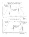
- the crystal oscillators of both the transmitter and receivershould be oscillating at almost exactly the same frequency. If not, part of the transmitted signal may be attenuated by the receiver's BPF. This is shown in FIG. 1 .
- Frequency response 12shows the frequency spectrum of a transmit signal 18 and the frequency operation of a receiver's Band Pass Filter (BPF) 16 .
- BPFBand Pass Filter
- Frequency response 14shows the frequency spectrum when the transmitter and receiver have crystal oscillators with different (offset) reference frequencies.
- the transmit signal 18is no longer centered within the BPF 16 . Any portion of the transmit signal 18 extending outside of BPF 16 is attenuated, such as the shaded portion 20 .
- the attenuation 20lowers the signal strength of signal 18 and can prevent the receiver from successfully or reliability receiving data carried in the transmit signal 18 .
- a radio systemmay operate at 2.4 GHz, with a 1 MHz channel spacing and a 900 kHz occupied bandwidth.
- a 50 parts per million (ppm) offsetis equal to 122.5 kHz.
- the occupied bandwidthis 100 kHz less than the channel spacing, there is 50 kHz on either side of a perfectly centered transmitter spectrum that is not part of the adjacent channel.
- the 50 ppm offset example7.2% of the transmitted signal extends into the adjacent channel.
- the receiver BPFis a little wider than the channel, and the roll-off of the filter is not a “brick wall”, so a small offset can be tolerated with minimal impact on receive sensitivity.
- a 50 ppm offsetis approximately the maximum that can be tolerated without significantly impacting performance.
- the receiver and transmitterare each subject to separate oscillator frequency inaccuracies. Therefore the receiver and transmitter require a crystal with an accuracy of better than +/ ⁇ 25 parts per million (ppm) to prevent the oscillator accuracy from impacting system performance with a combined worst case error of greater than 50 ppm.
- ppmparts per million
- Crystal oscillator accuracyis typically specified as three components; initial tolerance, temperature variation, and long-term drift. In order to put products in the best possible light, crystal oscillator vendors typically quote only the initial tolerance. Frequency variation with temperature is usually similar to the initial tolerance, and aging is usually in the range of one to five ppm per year.
- Crystalsgenerally drift in the same direction. Two instances of the same crystal would not usually drift in opposite directions, but they may well drift at different rates in the same direction.
- One factor affecting driftis the drive strength of the oscillator circuit driving the crystal.
- Another factormay be the proportion of time that the crystal oscillator is active. Over 5 years, a crystal with a 3 ppm/year drift spec may drift only 5 ppm (or less) or not at all, while another may drift 15 ppm. This crystal drift depends on drive strength, the amount of time that the oscillator is running, and the physical properties of the individual crystal.
- the frequency variation with temperatureis not linear, but rather typically a quadratic or cubic curve. Therefore, variations in temperature across only part of the rated range may cause frequency to vary over most of the stated tolerance.
- a 25 ppm crystalwhich initially may appear to be suitable for uses in the wireless applications discussed above, may not in fact be suitable.
- Such a crystalwould typically have 25 ppm initial tolerance, 25 ppm variation over temperature, and 3 ppm/year drift.
- One such crystal, starting at 25 ppm, and operated at a temperature which caused the frequency to oscillate at close to its minimum frequency,may be oscillating at minus 50 ppm from its nominal after 5 years.
- Another crystal, starting at +25 ppm, at a different temperaturemay oscillate at +65 ppm from its nominal after 5 years, resulting in a difference of 115 ppm. This drift could severely impact the receive sensitivity of almost any 2.4 GHz radio system. Therefore, to meet the +/ ⁇ 25 ppm spec discussed above, a more expensive 10 ppm crystal is required.
- the cost savings from specifying a looser toleranceis low.
- one vendormay offer a 13 MHz 30 ppm crystal in volume at a given price, and the 50 ppm version of the same crystal may only be a few cents cheaper.
- crystals with tolerances below 30 ppmquickly become more expensive, and a 10 ppm crystal may typically cost 3 ⁇ to 5 ⁇ more than the 30 ppm crystal. Frequency accuracy requirements of a design may therefore place a significant cost burden on low cost wireless systems.
- ICsradio Integrated Circuits
- many low cost radio Integrated Circuitsinclude a feature allowing trimming of the initial crystal frequency. Typically, this is implemented by using a digitally trimmable capacitance.
- the oscillator frequencyis measured, and an appropriate trim factor is stored in non-volatile memory within the device. This trim factor is loaded into a radio Integrated Circuit (IC) after each reset and allows the digitally controlled capacitance of the crystal oscillator to tune the crystal frequency to a nominal value. This removes the initial tolerance component of the oscillator, reducing the variation to just the temperature and drift components.
- Wireless devicestransmit and receive radio signals based upon reference frequencies that are generated by reference frequency circuits. If the reference frequency in the transmitter is different from the reference frequency in the receiver, the radio signals may not be received properly or may not be capable of being received at all.
- a measurement circuitmeasures the amount of error or signal corruption in radio signals due to the reference frequency offset.
- a trimming circuitthen tunes the reference frequency in the transmitter or receiver to reduce the reference frequency offset.
- FIG. 1shows attenuation of a transmitted signal when the transmitter and receiver reference frequencies are offset.
- FIG. 2shows an exemplary implementation of a system that provides reference frequency compensation.
- FIGS. 3 and 4show one example of how the reference frequency is compensated in FIG. 2 .
- FIG. 5shows a radio device that provides reference frequency compensation.
- FIG. 6is a detailed diagram of a crystal oscillator frequency trim circuit that can be used in the radio shown in FIG. 5 .
- FIG. 7is one example of radio transmit circuitry that provides reference frequency compensation.
- FIG. 8is one example of radio receive circuitry that provides reference frequency compensation.
- FIG. 9is a block diagram showing how reference frequency compensation can alternatively be performed within a frequency synthesizer.
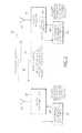
- FIG. 2shows reference frequency tuning system 21 that tunes the reference frequency of a radio receiver 34 with the reference frequency of a radio transmitter 22 .
- the radio transmitter 22includes an antenna 26 that transmits signals 28 that are received by the antenna 32 of receiver 34 .
- the radio receiver 34calculates signal quality information 33 associated with the received signal 28 and then uses that signal quality information 33 to adjust the reference frequency 38 used by the radio receiver 34 for demodulating the transmit signal 28 .
- a trimming operationis performed in the reference frequency generation circuit 36 that tunes the output frequency 38 to the frequency 25 used by the reference frequency circuit 24 in the transmitter 22 .
- the reference frequency 38 in the receiver 34is varied until it is tuned (zero offset) with the reference frequency 25 in the transmitter 22 .
- Signal quality information 33can be any signal measurement or statistic that indicates the transmitter 22 and the receiver 34 have offset reference frequencies.
- the signal quality information 33may be a Bit Error Rate (BER), packet error rate, signal strength, or any other indicator of frequency offset. Calculating these signal quality measurements have been used for other purposes in the past, and are therefore known to those skilled in the art, and are therefore not described in further detail.
- BERBit Error Rate
- the receiver 34may send the signal quality measurements 33 back to the transmitter 22 in signal 30 .
- the transmitter 22then trims its reference frequency 25 according to the signal quality measurements 33 in signal 30 .
- the signal 30may just carry the ppm value for the desired frequency offset to use for reference frequency 25 .
- the transmitter 22varies the reference frequency 25 until the signal quality information 33 identified in reply signal 30 is within an acceptable level.
- the tuning system 21may use a single frequency in normal operation (one of many channels available) or may use a frequency hopping system such as used in Frequency Hopping Spread Spectrum (FHSS) systems.
- the tuning system 21can also use a single point to point (1-1) radio link or can be implemented in a network of wireless devices, with an overall network coordinator or master.
- the transmitter 22 and receiver 34operate exactly on a pre-determined nominal frequency.
- the transmitter 22 and receiver 34may be designed to operate at a nominal frequency of 2450 MHz.
- the radioscan work equally as well if both are centered at 2450.1 MHz.
- the receiver 34will not completely fail to receive the transmitted signal. Instead, the Bit Error rate (BER) on the wireless link 28 will be very high. This will often make it difficult for the receiver 34 to successfully receive significant quantities of transmitted data, but the receiver 34 will still be aware that the signal 28 is being transmitted. Sufficient data will get though so that the receiver 34 will be able to recognize the transmitter 22 as its counterpart, rather than an interfering signal.
- BERBit Error rate
- each wireless deviceincludes both a radio transmitter and receiver
- only one of the wireless devicesmight incorporate the reference frequency trimming operation.
- the frequency trimming operationmight be incorporated in each of the slaves, which would then seek to tune their radios to the master device.
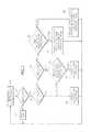
- FIGS. 3 and 4show one example of how the reference frequency is turned in the reference frequency circuits 24 or 36 in FIG. 2 .
- the tuning operations described in FIGS. 3 and 4can be performed in the receiver 34 ( FIG. 2 ) or can be performed in the transmitter 22 ( FIG. 2 ).
- the description in FIGS. 3 and 4will refer to the frequency trimming operation as being performed in the receiver 34 .
- the transmitter 22( FIG. 2 ) sends data to the receiver 34 and the receiver 34 demodulate the received data in block 40 of FIG. 3 .
- the datamay be successfully received. For example, there may be sufficiently few bit errors after error correction techniques have corrected the data.
- the receiver in block 40accordingly sends back an acknowledge handshake packet to the transmitter and the transaction completes.
- the bit error rate in the datamay be uncorrectable.
- the receiver 34will not respond.
- the transmitter 22will then retransmit the data packet.
- the receiver in block 44stores a measure of the bit error rate of the corrupted packet.
- the receiverthen changes its oscillator trim capacitance attempting to correct for an inferred oscillator frequency offset between the transmitter and receiver.
- An example of the frequency offset between the transmitter 22 and receiver 34is represented by initial frequency response 60 A in FIG. 4 .
- the initial frequency response 60 Ashows the transmit signal 28 offset from the expected frequency response of the Band Pass Filter (BPF) 59 of the receiver 34 . This is similar to the frequency response 14 shown in FIG. 1 .
- the initial offset frequency response 60 Aresults in the transmit signal 28 generating a high BER in block 44 of FIG. 3 .
- the receivershifts its oscillator frequency by 25 ppm in a random direction in block 48 . This of course is just one example and other shift values can also be used.
- the receiver reference frequencyis shifted +25 ppm and is shown graphically as first trim stage 60 B in FIG. 4 .
- the receiver 34then waits for the transmitter 22 to transmit another packet.
- the initial +25 ppm trim in the first trim stagemay have provided the desired result by reducing the BER below some threshold value in block 44 of FIG. 3 . Accordingly, the receiver 34 sends an acknowledge to the transmitter 22 in block 42 confirming to the transmitter 22 that the receiver 34 is now operating at the same, or substantially the same, oscillator frequency. The receiver 34 stores the trim value and continues to use that oscillator trim setting until a future uncorrectable packet is received.
- the BER in block 44may still be above some BER threshold after the first trim stage 60 B.
- the receiver 34first compares the BER of first trim stage 60 B with the initial signal response 60 A ( FIG. 4 ). If the first trim stage 60 B improved the BER in block 52 , the receiver 34 infers that the oscillator frequency was trimmed in the correct direction, but not far enough. In this case, the receiver 34 trims its crystal another 25 ppm in the same direction in block 48 .
- the first trim stage 60 Bmay make the BER worse than initial signal response 60 A. This is the case in FIG. 4 where the first trim stage 60 B moves the transmit signal 28 further outside of BPF 59 .
- the receiver 34infers that the oscillator frequency was trimmed in the wrong direction and trims the oscillator frequency 50 ppm in the opposite direction in block 54 . This is 25 ppm on the other side of the original frequency and is shown as second trim stage 60 C in FIG. 4 .
- the processis repeated.
- the BER rateis still above the BER threshold value in block 44 after the second trim stage 60 C.
- the BER after the second trim stage 60 Cis better then the BER of the previous trim stage 60 B.
- the receiver 34trims the oscillator frequency another 25 ppm in the same direction as the previous trim stage. This is shown as third trim stage 60 D in FIG. 4 that shifts the reference frequency in the receiver another 25 ppm.
- the BER rate for the third trim stage 60 Dis still above the BER rate threshold in block 44 .
- the receiver in block 57again trims the crystal oscillator frequency another 25 ppm in block 57 . This is shown as the fourth trim stage 60 E in FIG. 4 . After the fourth trim stage 60 E, the BER rate is now within an acceptable range in block 44 .
- the receiver 34accordingly sends the acknowledge signal to the transmitter 22 in block 42 .
- a timeoutmay occur due to the presence of an on-band interfering signal, or because the transmitter and receiver are further apart in distance than the operating range of the wireless link can support.
- Uncorrectable packetsmay therefore be received for a reason other than reference frequency offset. In this case, the receiver would not try shifting its oscillator trim value until a number of successive uncorrectable packets had been received.
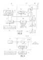
- FIG. 5shows in more detail an example of circuitry that may exist in the transmitter 22 or receiver 34 for trimming a reference frequency.
- An antenna 66receives or transmits wireless signals.
- a radio transceiver 68is coupled to the antenna 66 and communicates to a microcontroller 62 through a logic interface 70 .
- the untrimmed reference frequency 75 for the radio transceiver 68is generated by a crystal oscillator 74 .
- a crystal oscillator frequency trim circuit 72varies or “trims” the untrimmed base frequency of the crystal oscillator 74 and outputs the trimmed frequency 75 to the radio transceiver 68 . Adjustment of the base frequency of the crystal oscillator 74 can be controlled by logic in the radio transceiver 68 or by the microcontroller 62 .
- the original specified frequency crystal oscillator 74may change.
- the frequency 75is varied by trim circuit 72 as described above in FIGS. 3 and 4 to compensate for the frequency offset between the transmitter and receiver.
- FIG. 6shows one example of the crystal oscillator frequency trim circuit 72 in FIG. 5 .
- An amplifier 82 with hysteresisis coupled across opposite ends of the crystal oscillator 74 .
- a set of capacitors 84are selectively coupled to the amplifier 82 by switches that are activated by signals 80 .
- the signals 80are generated by the microcontroller 62 ( FIG. 5 ) through the logic interface 70 .
- the capacitors 84are selectively connected or disconnected from the amplifier 82 to vary the base frequency of the crystal oscillator 74 .
- the varied frequency 75is output to the radio transceiver 68 .
- FIG. 7shows one example of the functions that may be contained in the radio transceiver 68 in FIG. 5 or inside the transmitter 22 shown in FIG. 2 . Again, this is only an example and any type of transmitter circuitry can be used.
- a frequency synthesizer 86receives the trimmed crystal oscillator frequency 75 from the trim circuit 72 .
- the frequency synthesizer 86includes a phase detector ( FIG. 9 ) that receives the output 75 of the crystal oscillator trim circuit 72 and outputs a signal to a Voltage Controlled Oscillator (VCO) ( FIG. 9 ).
- the output frequency 87is equal to the crystal oscillator frequency 75 multiplied by a devisor in a feedback loop.
- the divideris used to set the operating channel for the transmitter.
- the frequency synthesizer 86generates output carrier frequency 88 that is mixed with the transmit data 92 by a mixer 91 .
- the output from the mixer 91is amplified by an amplifier 90 and output over antenna 66 .
- the microprocessor 62is connected to the amplifier 90 through logic interface 70 .
- FIG. 8shows a diagram of the receive circuitry that may exist inside the radio transceiver 68 or inside the receiver 34 shown in FIG. 2 .
- the trim circuit 72again feeds the trimmed crystal oscillator frequency 75 to a frequency synthesizer 94 similar to frequency synthesizer 86 in FIG. 7 .
- the output frequency generated from the synthesizer 94is mixed with the signal received over antenna 66 by mixer 96 .
- the output of the mixer 96is filtered by a Band Pass Filter (BPF) 59 as shown in the example of FIG. 4 .
- the output of the BPF 59is FM demodulated by demodulator 102 and output as receive data 104 .
- BPFBand Pass Filter
- FIG. 9shows one alternative embodiment where the crystal oscillator frequency is trimmed by varying the output frequency of the frequency synthesizer 86 or 94 in FIG. 7 or 8 , respectively.
- a programmable frequency divider 114is coupled between a phase detector 110 and the output of a VCO 112 that varies the output frequency 87 of the frequency synthesizer 86 or 94 .
- the microcontroller 62varies the output frequency of the synthesizer 86 or 94 .
- the output frequency 87is varied to again compensate for frequency offset between the transmitter and receiver.
- the frequency of output 87is varied by the microcontroller 62 by digitally varying the value in the frequency divider 114 .
- the digital value of the frequency divider 114can vary the frequency of the output signal 87 or 88 in both a positive ppm and negative ppm direction.
- the same iterative process shown in FIGS. 3 and 4is performed where the value of the frequency of output signal 87 or 88 is repeatedly varied by the microcontroller 62 until the BER or signal strength of the received data signal is within some acceptable value.
- RSSIReceived Signal Strength Indicator
- the RSSI 98is typically used to detect relative differences of as little as 1 dB in signal strength reliably.
- the RSSI 98is typically measured after the receiver band pass filter (BPF) 59 .
- BPFreceiver band pass filter
- the relative signal strength indicated by the RSSI 98is a good indication of the relative closeness of the receiver oscillator trim frequency 75 to the oscillator frequency in the transmitter.
- the crystal oscillator trim valuesare varied until the RSSI is at the maximum value achievable within the oscillator trimming range.
- the transmitter 22begins by sending a transmission to the receiver to establish a “session”. The transmitter 22 sends special test transmissions, until it receives a response from the receiver 34 indicating the tuning process has completed.
- the receiver 34may use a successive approximation method to bring its oscillator frequency close to the oscillator frequency in the transmitter 22 . It is the nature of wireless communications that the BER and RSSI may vary somewhat from transmission to transmission, even with all settings the same. In such a case, the receiver 34 can take average BER or RSSI readings over several transmissions before changing trim settings in circuit 72 or in synthesizer 94 . After this training session is complete, the transmitter 22 is ready to transmit data, without the risk that data packets may be delayed by multiple retransmissions. In this way, it is possible for the transmitter 22 and receiver 34 to achieve improved range/performance compared with a traditional system using even the most accurate (and costly) crystals.
- the “training session” approachmay be more suitable.
- the transmitter 22makes a number of packet training transmissions, to which the receiver 34 tunes, before the transmitter 22 begins transmitting “real” data.
- the “training session’ approachgenerally may be more suitable, because of the difficulty of managing handshakes from many receivers.
- the transmitter 22 or the receiver 34may intentionally reduce the gain of the transmitted or received signal in order to more quickly and precisely trim the crystal oscillator frequency.
- the distance between the transmitter 22 and receive 34may be close enough and the signal strength strong enough so that the BER is within some acceptable range, and the BER is so low that it is difficult for the receiver 34 to accurately trim the crystal oscillator frequency.
- the transmitter and receiverare so close, the effects of reference frequency offset cannot be accurately detected.
- the crystal oscillator frequency offsetmay cause problems with the signal transmission.
- the transmitter 22 in FIG. 7may include a variable amplifier 90 that can be turned down during the crystal oscillator frequency training session.
- the gain of the transmit signal 28is intentionally reduced so that the receiver 34 can more effectively determine how much, if any, frequency offset exists between the transmitter 22 and receiver 34 .
- the receiver 34 in FIG. 8can include a variable amplifier 97 that is intentionally turned down during the training session. After frequency trimming is complete in either the transmitter 22 and/or receive 34 , the amplifiers 90 ( FIG. 7 ) and/or amplifier 97 ( FIG. 8 ) is returned to their normal operating levels.
- the transmitter 22 and receiver 34may not stay long enough on a single frequency to complete either a training session or multiple retransmissions on a single frequency.
- the carrier frequency of each channelis derived from the same base crystal frequency
- either the training session method, or the multiple retry methodmay be applied. The only difference is that successive retries or successive transmissions within the training session will be on different channels.
- the transmitter 22 and receiver 34may include temperature sensors 120 ( FIG. 5 ).
- the transmitter 22 or receiver 34 in FIG. 5may include firmware that is executed on the microcontroller (MCU) 62 that monitors the temperature sensor 120 .
- MCUmicrocontroller
- either the transmitter 22 or the receiver 34may initiate a new training session any time a temperature change of more than a pre-determined amount is detected by temperature sensor 120 .
- either the transmitter 22 or the receiver 34may initiate a training session periodically, for example once per day.
- Reference frequency tuninghas many advantages, including enabling the use of low cost, low precision crystals in wireless systems.
- a further advantageis that transmitters and receivers can tune their oscillators to each other, enabling better receive sensitivity with low cost crystals than what is generally possible even with the most accurate and expensive crystals.
- the system described abovecan use dedicated processor systems, micro controllers, programmable logic devices, or microprocessors that perform some or all of the operations. Some of the operations described above may be implemented in software and other operations may be implemented in hardware.
Landscapes
- Transceivers (AREA)
Abstract
Description
Claims (19)
Priority Applications (1)
| Application Number | Priority Date | Filing Date | Title |
|---|---|---|---|
| US13/149,672US8521097B1 (en) | 2003-12-23 | 2011-05-31 | Method and apparatus for tuning a radio receiver with a radio transmitter |
Applications Claiming Priority (4)
| Application Number | Priority Date | Filing Date | Title |
|---|---|---|---|
| US53275303P | 2003-12-23 | 2003-12-23 | |
| US11/006,998US7787829B1 (en) | 2003-12-23 | 2004-12-07 | Method and apparatus for tuning a radio receiver with a radio transmitter |
| US87181410A | 2010-08-30 | 2010-08-30 | |
| US13/149,672US8521097B1 (en) | 2003-12-23 | 2011-05-31 | Method and apparatus for tuning a radio receiver with a radio transmitter |
Related Parent Applications (1)
| Application Number | Title | Priority Date | Filing Date |
|---|---|---|---|
| US87181410AContinuation | 2003-12-23 | 2010-08-30 |
Publications (1)
| Publication Number | Publication Date |
|---|---|
| US8521097B1true US8521097B1 (en) | 2013-08-27 |
Family
ID=42646708
Family Applications (2)
| Application Number | Title | Priority Date | Filing Date |
|---|---|---|---|
| US11/006,998Active2027-01-03US7787829B1 (en) | 2003-12-23 | 2004-12-07 | Method and apparatus for tuning a radio receiver with a radio transmitter |
| US13/149,672Expired - Fee RelatedUS8521097B1 (en) | 2003-12-23 | 2011-05-31 | Method and apparatus for tuning a radio receiver with a radio transmitter |
Family Applications Before (1)
| Application Number | Title | Priority Date | Filing Date |
|---|---|---|---|
| US11/006,998Active2027-01-03US7787829B1 (en) | 2003-12-23 | 2004-12-07 | Method and apparatus for tuning a radio receiver with a radio transmitter |
Country Status (1)
| Country | Link |
|---|---|
| US (2) | US7787829B1 (en) |
Cited By (2)
| Publication number | Priority date | Publication date | Assignee | Title |
|---|---|---|---|---|
| CN104320166A (en)* | 2014-09-10 | 2015-01-28 | 深圳市豪恩安全科技有限公司 | Method for realizing greatest-distance wireless transmission between wireless transceivers |
| US20190097864A1 (en)* | 2016-04-26 | 2019-03-28 | Diehl Metering Systems Gmbh | Method and apparatus for bidirectional communication between measuring devices and a data collector |
Families Citing this family (5)
| Publication number | Priority date | Publication date | Assignee | Title |
|---|---|---|---|---|
| US7787829B1 (en) | 2003-12-23 | 2010-08-31 | Cypress Semiconductor Corporation | Method and apparatus for tuning a radio receiver with a radio transmitter |
| JP2010011376A (en)* | 2008-06-30 | 2010-01-14 | Kddi Corp | Receiver using multiple bandwidths other than existing service bandwidths, program, and method |
| US9419746B1 (en)* | 2014-05-16 | 2016-08-16 | Altera Corporation | Apparatus and methods for tuning a communication link for power conservation |
| WO2018098622A1 (en)* | 2016-11-29 | 2018-06-07 | Microsoft Technology Licensing, Llc. | Adaptive frequency calibration |
| DE102017206236A1 (en)* | 2017-04-11 | 2018-10-11 | Fraunhofer-Gesellschaft zur Förderung der angewandten Forschung e.V. | SPECIFIC HOPPING PATTERN FOR TELEGRAM SPLITTING |
Citations (35)
| Publication number | Priority date | Publication date | Assignee | Title |
|---|---|---|---|---|
| US5260671A (en)* | 1991-05-17 | 1993-11-09 | Hitachi, Ltd. | Receiving circuit for demodulating an angle modulated signal |
| US5745523A (en)* | 1992-10-27 | 1998-04-28 | Ericsson Inc. | Multi-mode signal processing |
| US5748621A (en)* | 1995-03-10 | 1998-05-05 | Kabushiki Kaisha Toshiba | Digital mobile communication system |
| US5898903A (en) | 1996-03-14 | 1999-04-27 | Alligator Communications, Inc. | Multiple address radio system having automatic radio calibration for reducing frequency offset between radio frequency carriers |
| US6052036A (en)* | 1997-10-31 | 2000-04-18 | Telefonaktiebolaget L M Ericsson | Crystal oscillator with AGC and on-chip tuning |
| US6058291A (en) | 1997-12-03 | 2000-05-02 | 3Com Corporation | Methods and apparatus for carrier suppression in a radio modulator |
| US6072842A (en)* | 1996-11-21 | 2000-06-06 | Dsp Group, Inc. | Carrier-recovery loop with stored initialization in a radio receiver |
| US6081700A (en)* | 1996-12-17 | 2000-06-27 | Motorola, Inc. | Radio having a self-tuning antenna and method thereof |
| US6108525A (en)* | 1997-08-06 | 2000-08-22 | Nec Corporation | Transceiver |
| US6128468A (en)* | 1997-03-25 | 2000-10-03 | Ico Services Ltd. | Satellite communications terminal location system and method |
| US6215295B1 (en) | 1997-07-25 | 2001-04-10 | Smith, Iii Richard S. | Photonic field probe and calibration means thereof |
| US20010022539A1 (en)* | 2000-03-17 | 2001-09-20 | Peter Jakobsson | Electronic circuit |
| US20010044288A1 (en)* | 2000-05-17 | 2001-11-22 | Markus Zumkeller | AM receiver |
| US6337604B1 (en)* | 1999-05-14 | 2002-01-08 | Telefonaktiebolaget Lm Ericsson (Publ) | Crystal oscillator |
| US6377640B2 (en)* | 1997-07-31 | 2002-04-23 | Stanford Syncom, Inc. | Means and method for a synchronous network communications system |
| US6522696B1 (en)* | 1997-04-11 | 2003-02-18 | Agere Systems Inc. | Adaptive frequency correction in a wireless communications system, such as for GSM and IS54 |
| US6647276B1 (en) | 1999-09-14 | 2003-11-11 | Hitachi, Ltd. | Antenna unit and radio base station therewith |
| US6668025B1 (en)* | 1998-01-23 | 2003-12-23 | Matsushita Electric Industrial Co., Ltd. | Tuning demodulator for digitally modulated RF signals |
| US20040037365A1 (en)* | 2002-08-21 | 2004-02-26 | King Ronald O. | Remote transmitter system and method |
| US20040148580A1 (en)* | 2003-01-17 | 2004-07-29 | Texas Instruments Incorporated | On-chip receiver sensitivity test mechanism |
| US20040146098A1 (en)* | 2003-01-17 | 2004-07-29 | Texas Instruments Incorporated | Modulation noise estimation mechanism |
| US6882831B2 (en) | 2001-12-07 | 2005-04-19 | Broadcom Corporation | Translational loop transmitter architecture employing channel power ratio measurements for modulation accuracy calibration |
| US20050085249A1 (en) | 2003-10-16 | 2005-04-21 | Pctel, Inc. | Method, apparatus and system for pilotless frequency offset compensation in multipoint-to-point wireless systems with OFDM |
| US20050123036A1 (en)* | 2003-12-08 | 2005-06-09 | Mahibur Rahman | Method and apparatus for controlling the bandwidth frequency of an analog filter |
| US20050169357A1 (en)* | 2004-02-04 | 2005-08-04 | Hossein Sedarat | Reliable multicarrier communication in the presence of timing phase error |
| US6933788B2 (en)* | 2001-05-16 | 2005-08-23 | Kyocera Wireless Corp. | Reference oscillator |
| US6952124B2 (en)* | 2003-09-15 | 2005-10-04 | Silicon Bridge, Inc. | Phase locked loop circuit with self adjusted tuning hiep the pham |
| US6980823B2 (en) | 2002-01-31 | 2005-12-27 | Qualcomm Inc. | Intermediate wake mode to track sleep clock frequency in a wireless communication device |
| US7031676B2 (en) | 2001-12-07 | 2006-04-18 | Broadcom Corporation | Radio frequency transmitter having translational loop phase equalization |
| US7066643B2 (en) | 2003-12-22 | 2006-06-27 | Sunplus Technology Co,Ltd. | Radio frequency temperature sensor and method of calibrating temperature therefor |
| US7113744B1 (en)* | 1999-10-21 | 2006-09-26 | Broadcom Corporation | Adaptive radio transceiver with a power amplifier |
| US20070127562A1 (en)* | 2005-12-07 | 2007-06-07 | Gehring Mark R | Apparatus and method for frequency calibration between two radios |
| US7269394B2 (en) | 2002-10-02 | 2007-09-11 | Agere Systems Inc. | Frequency offset compensation for communication systems |
| US7630463B2 (en) | 2004-11-15 | 2009-12-08 | Samsung Electronics Co., Ltd. | Apparatus and method for acquiring synchronization in mobile communication system using OFDM scheme |
| US7787829B1 (en) | 2003-12-23 | 2010-08-31 | Cypress Semiconductor Corporation | Method and apparatus for tuning a radio receiver with a radio transmitter |
- 2004
- 2004-12-07USUS11/006,998patent/US7787829B1/enactiveActive
- 2011
- 2011-05-31USUS13/149,672patent/US8521097B1/ennot_activeExpired - Fee Related
Patent Citations (41)
| Publication number | Priority date | Publication date | Assignee | Title |
|---|---|---|---|---|
| US5260671A (en)* | 1991-05-17 | 1993-11-09 | Hitachi, Ltd. | Receiving circuit for demodulating an angle modulated signal |
| US5745523A (en)* | 1992-10-27 | 1998-04-28 | Ericsson Inc. | Multi-mode signal processing |
| US5748621A (en)* | 1995-03-10 | 1998-05-05 | Kabushiki Kaisha Toshiba | Digital mobile communication system |
| US5898903A (en) | 1996-03-14 | 1999-04-27 | Alligator Communications, Inc. | Multiple address radio system having automatic radio calibration for reducing frequency offset between radio frequency carriers |
| US6072842A (en)* | 1996-11-21 | 2000-06-06 | Dsp Group, Inc. | Carrier-recovery loop with stored initialization in a radio receiver |
| US6081700A (en)* | 1996-12-17 | 2000-06-27 | Motorola, Inc. | Radio having a self-tuning antenna and method thereof |
| US6128468A (en)* | 1997-03-25 | 2000-10-03 | Ico Services Ltd. | Satellite communications terminal location system and method |
| US6522696B1 (en)* | 1997-04-11 | 2003-02-18 | Agere Systems Inc. | Adaptive frequency correction in a wireless communications system, such as for GSM and IS54 |
| US6215295B1 (en) | 1997-07-25 | 2001-04-10 | Smith, Iii Richard S. | Photonic field probe and calibration means thereof |
| US6377640B2 (en)* | 1997-07-31 | 2002-04-23 | Stanford Syncom, Inc. | Means and method for a synchronous network communications system |
| US6108525A (en)* | 1997-08-06 | 2000-08-22 | Nec Corporation | Transceiver |
| US6052036A (en)* | 1997-10-31 | 2000-04-18 | Telefonaktiebolaget L M Ericsson | Crystal oscillator with AGC and on-chip tuning |
| US6058291A (en) | 1997-12-03 | 2000-05-02 | 3Com Corporation | Methods and apparatus for carrier suppression in a radio modulator |
| US6668025B1 (en)* | 1998-01-23 | 2003-12-23 | Matsushita Electric Industrial Co., Ltd. | Tuning demodulator for digitally modulated RF signals |
| US6337604B1 (en)* | 1999-05-14 | 2002-01-08 | Telefonaktiebolaget Lm Ericsson (Publ) | Crystal oscillator |
| US6647276B1 (en) | 1999-09-14 | 2003-11-11 | Hitachi, Ltd. | Antenna unit and radio base station therewith |
| US7113744B1 (en)* | 1999-10-21 | 2006-09-26 | Broadcom Corporation | Adaptive radio transceiver with a power amplifier |
| US6559731B2 (en)* | 2000-03-17 | 2003-05-06 | Telefonaktiebolaget Lm Ericsson (Publ) | VCXO temperature compensation circuit |
| US20010022539A1 (en)* | 2000-03-17 | 2001-09-20 | Peter Jakobsson | Electronic circuit |
| US7155189B2 (en)* | 2000-05-17 | 2006-12-26 | Sony Deutschland Gmbh | AM receiver |
| US20010044288A1 (en)* | 2000-05-17 | 2001-11-22 | Markus Zumkeller | AM receiver |
| US7098749B2 (en)* | 2001-05-16 | 2006-08-29 | Kyocera Wireless Corp. | Reference oscillator |
| US6933788B2 (en)* | 2001-05-16 | 2005-08-23 | Kyocera Wireless Corp. | Reference oscillator |
| US6882831B2 (en) | 2001-12-07 | 2005-04-19 | Broadcom Corporation | Translational loop transmitter architecture employing channel power ratio measurements for modulation accuracy calibration |
| US7031676B2 (en) | 2001-12-07 | 2006-04-18 | Broadcom Corporation | Radio frequency transmitter having translational loop phase equalization |
| US6980823B2 (en) | 2002-01-31 | 2005-12-27 | Qualcomm Inc. | Intermediate wake mode to track sleep clock frequency in a wireless communication device |
| US20040037365A1 (en)* | 2002-08-21 | 2004-02-26 | King Ronald O. | Remote transmitter system and method |
| US7269394B2 (en) | 2002-10-02 | 2007-09-11 | Agere Systems Inc. | Frequency offset compensation for communication systems |
| US20040148580A1 (en)* | 2003-01-17 | 2004-07-29 | Texas Instruments Incorporated | On-chip receiver sensitivity test mechanism |
| US7254755B2 (en)* | 2003-01-17 | 2007-08-07 | Texas Instruments Incorporated | On-chip receiver sensitivity test mechanism |
| US20040146098A1 (en)* | 2003-01-17 | 2004-07-29 | Texas Instruments Incorporated | Modulation noise estimation mechanism |
| US7460499B2 (en) | 2003-01-17 | 2008-12-02 | Texas Instruments Incorporated | Modulation noise estimation mechanism |
| US6952124B2 (en)* | 2003-09-15 | 2005-10-04 | Silicon Bridge, Inc. | Phase locked loop circuit with self adjusted tuning hiep the pham |
| US20050085249A1 (en) | 2003-10-16 | 2005-04-21 | Pctel, Inc. | Method, apparatus and system for pilotless frequency offset compensation in multipoint-to-point wireless systems with OFDM |
| US20050123036A1 (en)* | 2003-12-08 | 2005-06-09 | Mahibur Rahman | Method and apparatus for controlling the bandwidth frequency of an analog filter |
| US7066643B2 (en) | 2003-12-22 | 2006-06-27 | Sunplus Technology Co,Ltd. | Radio frequency temperature sensor and method of calibrating temperature therefor |
| US7787829B1 (en) | 2003-12-23 | 2010-08-31 | Cypress Semiconductor Corporation | Method and apparatus for tuning a radio receiver with a radio transmitter |
| US20050169357A1 (en)* | 2004-02-04 | 2005-08-04 | Hossein Sedarat | Reliable multicarrier communication in the presence of timing phase error |
| US7433395B2 (en) | 2004-02-04 | 2008-10-07 | 2Wire, Inc. | Reliable multicarrier communication in the presence of timing phase error |
| US7630463B2 (en) | 2004-11-15 | 2009-12-08 | Samsung Electronics Co., Ltd. | Apparatus and method for acquiring synchronization in mobile communication system using OFDM scheme |
| US20070127562A1 (en)* | 2005-12-07 | 2007-06-07 | Gehring Mark R | Apparatus and method for frequency calibration between two radios |
Non-Patent Citations (23)
| Title |
|---|
| Aeroflex Corporation, "Application Note: An Introduction to Digital and Vector Modulation," Part No. 46891/863, Issue 2, Aug. 2005; 10 pages. |
| Cypress Semiconductor Corporation, "WirelessUSB Crystal Guidelines," Revision Mar. 2005; 2 pages. |
| Cypress Semiconductor Corporation, "WirelessUSB LS Theory of Operation," Revision Aug. 2003; 4 pages. |
| Hewlett Packard, "Digital Modulation in Communications Systems-An Introduction-Application Note 1298," 1997; 47 pages. |
| International Search Report of the International Searching Authority for International Application No. PCT/US06/61658 mailed Nov. 20, 2007; 2 pages. |
| University of Saint Andrews, "Broadcasting and Communications 16.1 The Crowded Party," Copyright 1995-2006; 9 pages. |
| USPTO Advisory Action for U.S. Appl. No. 11/297,505 dated Sep. 11, 2009; 3 pages. |
| USPTO Final Rejection for U.S. Appl. No. 11/006,998 dated Jun. 2, 2008; 17 pages. |
| USPTO Final Rejection for U.S. Appl. No. 11/297,505 dated Jul. 6, 2009; 19 pages. |
| USPTO Non Final Rejection for U.S. Appl. No. 12/871,814 dated Feb. 28, 2011; 18 pages. |
| USPTO Non-Final Rejection for U.S. Appl. No. 11/006,998 dated Dec. 14, 2007; 17 pages. |
| USPTO Non-Final Rejection for U.S. Appl. No. 11/006,998 dated Jun. 21, 2007; 12 pages. |
| USPTO Non-Final Rejection for U.S. Appl. No. 11/006,998 dated May 27, 2009; 12 pages. |
| USPTO Non-Final Rejection for U.S. Appl. No. 11/006,998 dated Nov. 25, 2008; 14 pages. |
| USPTO Non-Final Rejection for U.S. Appl. No. 11/297,505 dated Jan. 15, 2009; 11 pages. |
| USPTO Notice of Allowance for U.S. Appl. No. 11/006,998 dated Dec. 23, 2009; 9 pages. |
| USPTO Notice of Allowance for U.S. Appl. No. 11/297,505 dated Oct. 21, 2009; 8 pages. |
| Wenzel Associates Inc., "Tuning Range," , Copyright 1995-2006; 5 pages. |
| Wenzel Associates Inc., "Tuning Range," <http://www.wenzel.com/documents/tuning.html>, Copyright 1995-2006; 5 pages. |
| William H. Pratt, "A Direct Quadrature Modulator IC for 0.9 to 2.5 GHz Wireless Systems," RF Design, Aug. 1994; 5 pages. |
| Written Opinion of the International Searching Authority for International Application No. PCT/US06/61658 mailed Nov. 20, 2007; 4 pages. |
| Zoka, Gabor, "Refined I/Q Imbalance Measurements," Microwaves & RF, http://www.mwrf.com/Articles/Print.cfm?ArticleID=8318, Jun. 2004, 8 pages. |
| Zolomy et al., "Antenna Tuning Technique Cuts Size, Cost in ISM Designs," Integration Associates, Jan. 2004; 7 pages. |
Cited By (4)
| Publication number | Priority date | Publication date | Assignee | Title |
|---|---|---|---|---|
| CN104320166A (en)* | 2014-09-10 | 2015-01-28 | 深圳市豪恩安全科技有限公司 | Method for realizing greatest-distance wireless transmission between wireless transceivers |
| CN104320166B (en)* | 2014-09-10 | 2018-04-17 | 中安消物联传感(深圳)有限公司 | The method that maximum distance is wirelessly transferred is realized between a kind of wireless transceiver |
| US20190097864A1 (en)* | 2016-04-26 | 2019-03-28 | Diehl Metering Systems Gmbh | Method and apparatus for bidirectional communication between measuring devices and a data collector |
| US10805142B2 (en)* | 2016-04-26 | 2020-10-13 | Diehl Metering Systems Gmbh | Method and apparatus for bidirectional communication between measuring devices and a data collector |
Also Published As
| Publication number | Publication date |
|---|---|
| US7787829B1 (en) | 2010-08-31 |
Similar Documents
| Publication | Publication Date | Title |
|---|---|---|
| US8521097B1 (en) | Method and apparatus for tuning a radio receiver with a radio transmitter | |
| US4921467A (en) | Local oscillators for radio receivers | |
| US7098749B2 (en) | Reference oscillator | |
| US8742863B1 (en) | Temperature-corrected frequency control with crystal oscillators for initial frequency acquisition | |
| US20050215219A1 (en) | Direct tuning of radio receiver integrated circuit | |
| WO2007067916A2 (en) | Apparatus and method for frequency calibration between two radios | |
| CN112039635B (en) | UART baud rate self-adaption method and device based on RC oscillator | |
| JPH1013181A (en) | System for automatic matching if filter | |
| TW201933798A (en) | Wireless system, calibration system and local oscillator signal calibration method | |
| US8350969B2 (en) | Electronic apparatus, electronic-apparatus adjustment method and integrated circuit | |
| US7123106B2 (en) | Frequency offset correction techniques for crystals used in communication systems | |
| CN108011633B (en) | Calibration method and device of RC oscillator, storage medium and processor | |
| JPH1155149A (en) | Transmitter/receiver | |
| EP0949758B1 (en) | Communications system, mobile device and method | |
| US7095815B2 (en) | Receiver and method for initial synchronization of a receiver with the carrier frequency of a desired channel | |
| WO2009019639A2 (en) | Crystal-less transceivers | |
| JP2009100416A (en) | Wireless system | |
| US7305219B2 (en) | Portable radio terminal and AFC control method | |
| JPS63281526A (en) | Mobile radio equipment having frequency stabilizing function | |
| JPS6326037A (en) | Mobile radio equipment | |
| JP3402359B2 (en) | Operation stabilizing apparatus and method | |
| JPH0722974A (en) | Temperature compensated radio receiver | |
| JP2011193528A (en) | Method and system for receiving dsss signal | |
| JPH04337928A (en) | transceiver | |
| KR100241787B1 (en) | Automatic Frequency Control Unit of Superheterodyne Receiver |
Legal Events
| Date | Code | Title | Description |
|---|---|---|---|
| AS | Assignment | Owner name:CYPRESS SEMICONDUCTOR CORPORATION, CALIFORNIA Free format text:ASSIGNMENT OF ASSIGNORS INTEREST;ASSIGNOR:WRIGHT, DAVID G.;REEL/FRAME:027757/0454 Effective date:20041203 | |
| STCF | Information on status: patent grant | Free format text:PATENTED CASE | |
| AS | Assignment | Owner name:MORGAN STANLEY SENIOR FUNDING, INC., NEW YORK Free format text:SECURITY INTEREST;ASSIGNORS:CYPRESS SEMICONDUCTOR CORPORATION;SPANSION LLC;REEL/FRAME:035240/0429 Effective date:20150312 | |
| FPAY | Fee payment | Year of fee payment:4 | |
| AS | Assignment | Owner name:MUFG UNION BANK, N.A., CALIFORNIA Free format text:ASSIGNMENT AND ASSUMPTION OF SECURITY INTEREST IN INTELLECTUAL PROPERTY;ASSIGNOR:MORGAN STANLEY SENIOR FUNDING, INC.;REEL/FRAME:050896/0366 Effective date:20190731 | |
| AS | Assignment | Owner name:MORGAN STANLEY SENIOR FUNDING, INC., NEW YORK Free format text:CORRECTIVE ASSIGNMENT TO CORRECT THE 8647899 PREVIOUSLY RECORDED ON REEL 035240 FRAME 0429. ASSIGNOR(S) HEREBY CONFIRMS THE SECURITY INTERST;ASSIGNORS:CYPRESS SEMICONDUCTOR CORPORATION;SPANSION LLC;REEL/FRAME:058002/0470 Effective date:20150312 | |
| MAFP | Maintenance fee payment | Free format text:PAYMENT OF MAINTENANCE FEE, 8TH YEAR, LARGE ENTITY (ORIGINAL EVENT CODE: M1552); ENTITY STATUS OF PATENT OWNER: LARGE ENTITY Year of fee payment:8 | |
| AS | Assignment | Owner name:SPANSION LLC, CALIFORNIA Free format text:RELEASE BY SECURED PARTY;ASSIGNOR:MUFG UNION BANK, N.A.;REEL/FRAME:059410/0438 Effective date:20200416 Owner name:CYPRESS SEMICONDUCTOR CORPORATION, CALIFORNIA Free format text:RELEASE BY SECURED PARTY;ASSIGNOR:MUFG UNION BANK, N.A.;REEL/FRAME:059410/0438 Effective date:20200416 | |
| FEPP | Fee payment procedure | Free format text:MAINTENANCE FEE REMINDER MAILED (ORIGINAL EVENT CODE: REM.); ENTITY STATUS OF PATENT OWNER: LARGE ENTITY | |
| LAPS | Lapse for failure to pay maintenance fees | Free format text:PATENT EXPIRED FOR FAILURE TO PAY MAINTENANCE FEES (ORIGINAL EVENT CODE: EXP.); ENTITY STATUS OF PATENT OWNER: LARGE ENTITY | |
| STCH | Information on status: patent discontinuation | Free format text:PATENT EXPIRED DUE TO NONPAYMENT OF MAINTENANCE FEES UNDER 37 CFR 1.362 |