US8519973B1 - Apparatus and methods for detecting a conductive object at a location - Google Patents
Apparatus and methods for detecting a conductive object at a locationDownload PDFInfo
- Publication number
- US8519973B1 US8519973B1US13/442,716US201213442716AUS8519973B1US 8519973 B1US8519973 B1US 8519973B1US 201213442716 AUS201213442716 AUS 201213442716AUS 8519973 B1US8519973 B1US 8519973B1
- Authority
- US
- United States
- Prior art keywords
- capacitance
- sensor
- processing device
- button
- sense
- Prior art date
- Legal status (The legal status is an assumption and is not a legal conclusion. Google has not performed a legal analysis and makes no representation as to the accuracy of the status listed.)
- Active
Links
Images


Classifications
- G—PHYSICS
- G06—COMPUTING OR CALCULATING; COUNTING
- G06F—ELECTRIC DIGITAL DATA PROCESSING
- G06F3/00—Input arrangements for transferring data to be processed into a form capable of being handled by the computer; Output arrangements for transferring data from processing unit to output unit, e.g. interface arrangements
- G06F3/01—Input arrangements or combined input and output arrangements for interaction between user and computer
- G06F3/03—Arrangements for converting the position or the displacement of a member into a coded form
- G06F3/041—Digitisers, e.g. for touch screens or touch pads, characterised by the transducing means
- G06F3/044—Digitisers, e.g. for touch screens or touch pads, characterised by the transducing means by capacitive means
- G06F3/0446—Digitisers, e.g. for touch screens or touch pads, characterised by the transducing means by capacitive means using a grid-like structure of electrodes in at least two directions, e.g. using row and column electrodes
- G—PHYSICS
- G06—COMPUTING OR CALCULATING; COUNTING
- G06F—ELECTRIC DIGITAL DATA PROCESSING
- G06F3/00—Input arrangements for transferring data to be processed into a form capable of being handled by the computer; Output arrangements for transferring data from processing unit to output unit, e.g. interface arrangements
- G06F3/01—Input arrangements or combined input and output arrangements for interaction between user and computer
- G06F3/03—Arrangements for converting the position or the displacement of a member into a coded form
- G06F3/041—Digitisers, e.g. for touch screens or touch pads, characterised by the transducing means
- G06F3/044—Digitisers, e.g. for touch screens or touch pads, characterised by the transducing means by capacitive means
- G06F3/0445—Digitisers, e.g. for touch screens or touch pads, characterised by the transducing means by capacitive means using two or more layers of sensing electrodes, e.g. using two layers of electrodes separated by a dielectric layer
- G—PHYSICS
- G06—COMPUTING OR CALCULATING; COUNTING
- G06F—ELECTRIC DIGITAL DATA PROCESSING
- G06F2203/00—Indexing scheme relating to G06F3/00 - G06F3/048
- G06F2203/041—Indexing scheme relating to G06F3/041 - G06F3/045
- G06F2203/04111—Cross over in capacitive digitiser, i.e. details of structures for connecting electrodes of the sensing pattern where the connections cross each other, e.g. bridge structures comprising an insulating layer, or vias through substrate
Definitions
- This inventionrelates to the field of user interface devices and, in particular, to touch-sensing devices.
- Computing devicessuch as notebook computers, personal data assistants (PDAs), and mobile handsets, have user interface devices, which are also known as human interface device (HID).
- user interface deviceswhich are also known as human interface device (HID).
- One user interface device that is commonis a touch-sensor button.
- a basis touch-sensor buttonemulates the function of a mechanical button.
- Touch-sensor buttonsmay be embedded into different types of operational panels of electronic devices. For example, touch-sensor buttons may be used on operational or control panels of household appliances, consumer electronics, mechanical devices, and the like. Touch-sensor buttons may also be used in conjunction with, or in place of, other user input devices, such as keyboards, mice, trackballs, or the like.
- FIG. 1Aillustrates a conventional sensing device having three touch-sensor buttons.
- Conventional sensing device 100includes button 101 , button 102 , and button 103 . These buttons are conventional touch-sensor buttons. These three buttons may be used for user input using a conductive object, such as a finger.
- FIG. 1Billustrates a conventional sensing device of three touch-sensor buttons 101 - 103 coupled to a processing device 110 .
- Processing device 110is used to detect whether a conductive object is present on either, or none, of the touch-sensor buttons 101 - 103 .
- the processing device 110may include capacitance sensors 104 - 106 , which are coupled to buttons 101 - 103 , respectively.
- the capacitance sensors of the processing deviceare coupled to the touch-sensor buttons in a one-to-one configuration. Accordingly, the processing device 110 scans the touch-sensor buttons 101 - 103 using the capacitance sensors 104 - 106 , and measures the capacitance on the touch-sensor buttons 101 - 103 .
- Each of the conventional touch-sensor buttons 101 - 103may be made of a sensor element of conductive material, such as copper-clad.
- the conductive materialmay be form shaped in a circular shape (illustrated in FIG. 1A ), or even in a rectangular shape (illustrated in FIG. 1B ).
- the touch-sensor buttonsmay be capacitance sensor buttons, which may be used as non-contact switches. These switches, when protected by an insulating layer, offer resistance to severe environments.
- the conventional configuration of FIG. 1Bincludes a one-to-one configuration of touch-sensor buttons to capacitance sensors.
- These conventional configurationsstill require a one-to-one configuration of pins to touch-sensor buttons.
- the processing deviceneeds to have more pins to correspond to the one-to-one configuration of pins to touch-sensor buttons.
- the scan time to scan the sensor elementsincreases.
- the memory of the processing devicewhich may be used to store program data and/or temporary data (e.g., raw measurement data, differential counts, baseline measurement data, and the like), increases by increasing the pin count.
- FIG. 1Aillustrates a conventional sensing device having three touch-sensor buttons.
- FIG. 1Billustrates a conventional sensing device of three touch-sensor buttons coupled to a processing device.
- FIG. 2illustrates a block diagram of one embodiment of an electronic system having a processing device for detecting a presence of a conductive object.
- FIG. 3Aillustrates a varying switch capacitance
- FIG. 3Billustrates one embodiment of a relaxation oscillator.
- FIG. 4illustrates a block diagram of one embodiment of a capacitance sensor including a relaxation oscillator and digital counter.
- FIG. 5Aillustrates a top-side view of one embodiment of a sensor array having a plurality of sensor elements for detecting a presence of a conductive object on the sensor array of a touch-sensor pad.
- FIG. 5Billustrates a top-side view of one embodiment of a sensor array having a plurality of sensor elements for detecting a presence of a conductive object on the sensor array of a touch-sensor slider
- FIG. 5Cillustrates a top-side view of one embodiment of a two-layer touch-sensor pad.
- FIG. 5Dillustrates a side view of one embodiment of the two-layer touch-sensor pad of FIG. 5C .
- FIG. 6Aillustrates one embodiment of a sensing device having three touch-sensor buttons.
- FIG. 6Billustrates one embodiment of the sensing device of FIG. 6A coupled to a processing device.
- FIG. 6Cillustrates another embodiment of a sensing device having three touch-sensor buttons.
- FIG. 6Dillustrates another embodiment of a sensing device having three touch-sensor buttons.
- FIG. 7Aillustrates another embodiment of a sensing device having four touch-sensor buttons.
- FIG. 7Billustrates another embodiment of a sensing device having five touch-sensor buttons.
- Described hereinis an apparatus and method for detecting a presence of a conductive object on a sensing device, and recognizing three or more button operations performed by the conductive object using two sensing areas of the sensing device.
- the following descriptionsets forth numerous specific details such as examples of specific systems, components, methods, and so forth, in order to provide a good understanding of several embodiments of the present invention. It will be apparent to one skilled in the art, however, that at least some embodiments of the present invention may be practiced without these specific details. In other instances, well-known components or methods are not described in detail or are presented in simple block diagram format in order to avoid unnecessarily obscuring the present invention. Thus, the specific details set forth are merely exemplary. Particular implementations may vary from these exemplary details and still be contemplated to be within the spirit and scope of the present invention.
- the apparatusmay include a sensing device (e.g., touch-sensor button) that has first, second, and third sensor elements.
- the third sensor elementhas a first portion coupled to the first sensor element, and a second portion coupled to the second sensor element. These portions of the third sensor element are electrically isolated from one another.
- buttonse.g., three or more total buttons
- each button addedrequires an additional pin on the processing device.
- the scan timedoes not increase by adding additional buttons to implement three or more buttons on the sensing device.
- the scan time to scan the sensor elementsis not increased. In other words, more buttons may be implemented without increasing the total scan time of the sensing device.
- the memory of the processing deviceis not increased to accommodate additional program data and/or temporary data (e.g., raw measurement data, differential counts, baseline measurement data, and the like) for the additional buttons.
- the sensing devicemay use two capacitive switch relaxation oscillator (CSR) pins of a processing device to realize more than two buttons on the sensing device.
- the three or more buttonsmay be realized by using two sensing areas.
- Each sensing areamay include a bar of conductive material and several interconnected sub-bars.
- the sub-bars of the two sensing areasare interleaved and are electrically isolated. In other words, one set of interconnected sub-bars are connected to one pin, while the other set is coupled to the other pin.
- the two sensing areasmake up three or more sensor elements that are used to form the touch-sensor buttons.
- the different buttonscontain different percentages of surface area of the sensing areas.
- each sensing areamay include two or more bars of conductive material with or without several interconnected sub-bars.
- a three-button scheme using two pinsincludes one sensor element that has 100% of the first sensing area, the second sensor element has 50% of the first sensing area and 50% of the second sensing area, and the third sensor element has 100% of the second sensing area. Accordingly, by scanning and measuring the capacitance (e.g., capacitance variation of the capacitance minus the baseline, as described below) on the two pins to detect the presence of the conductive object, the processing device can distinguish between the presence of the conductive object on the first, second, and third sensor elements.
- the capacitancee.g., capacitance variation of the capacitance minus the baseline, as described below
- the first buttonhas been pressed.
- the capacitance variation ⁇ 1measured on the first pin
- the capacitance variation ⁇ 2measured on the second pin
- the second buttonhas been pressed. If the capacitance variation ⁇ 1 , measured on the first pin, is equal to approximately zero, and the capacitance variation ⁇ 2 , measured on the second pin is greater than zero, then the third button has been pressed.
- the embodiments hereinmay be beneficial to help reduce the pin count of the processing device. This may decrease the complexity of the processing device, or allow the processing device to support additional functionality, such as cursor positioning and selecting functionality, keyboard functionality, slider functionality, or the like. Furthermore, the embodiments may be beneficial to help reduce the scan time of the sensing device. Using two pins of the processing device to measure the capacitance on two sensing areas to realize three or more buttons is faster than measuring the capacitance on three or more touch-sensor buttons of the conventional configuration (e.g., one-to-one configuration). In addition, using two pins reduces the RAM/FLASH space needed in the sensing device, as compared to the conventional configuration.
- touch-sensor buttonsmay be used on operational or control panels of household appliances, consumer electronics, mechanical devices, and the like.
- Touch-sensor buttonsmay also be used in conjunction with, or in place of, other user input devices, such as keyboards, mice, trackballs, or the like.
- FIG. 2illustrates a block diagram of one embodiment of an electronic system having a processing device for detecting a presence of a conductive object.
- Electronic system 200includes processing device 210 , touch-sensor pad 220 , touch-sensor slider 230 , touch-sensor buttons 240 , host processor 250 , embedded controller 260 , and non-capacitance sensor elements 270 .
- the processing device 210may include analog and/or digital general purpose input/output (“GPIO”) ports 207 .
- GPIO ports 207may be programmable.
- GPIO ports 207may be coupled to a Programmable Interconnect and Logic (“PIL”), which acts as an interconnect between GPIO ports 207 and a digital block array of the processing device 210 (not illustrated).
- PILProgrammable Interconnect and Logic
- the digital block arraymay be configured to implement a variety of digital logic circuits (e.g., DAC, digital filters, digital control systems, etc.) using, in one embodiment, configurable user modules (“UMs”).
- the digital block arraymay be coupled to a system bus.
- Processing device 210may also include memory, such as random access memory (RAM) 205 and program flash 204 .
- RAM 205may be static RAM (SRAM), and program flash 204 may be a non-volatile storage, which may be used to store firmware (e.g., control algorithms executable by processing core 202 to implement operations described herein).
- Processing device 210may also include a memory controller unit (MCU) 203 coupled to memory and the processing core 202 .
- MCUmemory controller unit
- the processing device 210may also include an analog block array (not illustrated).
- the analog block arrayis also coupled to the system bus.
- Analog block arrayalso may be configured to implement a variety of analog circuits (e.g., ADC, analog filters, etc.) using, in one embodiment, configurable UMs.
- the analog block arraymay also be coupled to the GPIO 207 .
- capacitance sensor 201may be integrated into processing device 210 .
- Capacitance sensor 201may include analog I/O for coupling to an external component, such as touch-sensor pad 220 , touch-sensor slider 230 , touch-sensor buttons 240 , and/or other devices.
- Capacitance sensor 201 and processing device 202are described in more detail below.
- the embodiments described hereinare not limited to touch-sensor pads for notebook implementations, but can be used in other capacitive sensing implementations, for example, the sensing device may be a touch-sensor slider 230 , or a touch-sensor button 240 (e.g., capacitance sensing button).
- the operations described hereinare not limited to notebook cursor operations, but can include other operations, such as lighting control (dimmer), volume control, graphic equalizer control, speed control, or other control operations requiring gradual adjustments.
- these embodiments of capacitive sensing implementationsmay be used in conjunction with non-capacitive sensing elements, including but not limited to pick buttons, sliders (ex. display brightness and contrast), scroll-wheels, multi-media control (ex. volume, track advance, etc) handwriting recognition and numeric keypad operation.
- the electronic system 200includes a touch-sensor pad 220 coupled to the processing device 210 via bus 221 .
- Touch-sensor pad 220may include a multi-dimension sensor array.
- the multi-dimension sensor arraycomprises a plurality of sensor elements, organized as rows and columns.
- the electronic system 200includes a touch-sensor slider 230 coupled to the processing device 210 via bus 231 .
- Touch-sensor slider 230may include a single-dimension sensor array.
- the single-dimension sensor arraycomprises a plurality of sensor elements, organized as rows, or alternatively, as columns.
- the electronic system 200includes a touch-sensor button 240 coupled to the processing device 210 via bus 241 .
- Touch-sensor button 240may include a single-dimension or multi-dimension sensor array.
- the single- or multi-dimension sensor arraycomprises a plurality of sensor elements.
- the plurality of sensor elementsmay be coupled together to detect a presence of a conductive object over the entire surface of the sensing device.
- the touch-sensor button 240has a single sensor element to detect the presence of the conductive object.
- the touch-sensor button 240may be a capacitance sensor element. Capacitance sensor elements may be used as non-contact switches. These switches, when protected by an insulating layer, offer resistance to severe environments.
- the electronic system 200may include any combination of one or more of the touch-sensor pad 220 , touch-sensor slider 230 , and/or touch-sensor button 240 .
- the electronic system 200may also include non-capacitance sensor elements 270 coupled to the processing device 210 via bus 271 .
- the non-capacitance sensor elements 270may include buttons, light emitting diodes (LEDs), and other user interface devices, such as a mouse, a keyboard, or other functional keys that do not require capacitance sensing.
- buses 271 , 241 , 231 , and 221may be a single bus. Alternatively, these buses may be configured into any combination of one or more separate buses.
- the processing devicemay also provide value-added functionality such as keyboard control integration, LEDs, battery charger and general purpose I/O, as illustrated as non-capacitance sensor elements 270 .
- Non-capacitance sensor elements 270are coupled to the GPIO 207 .
- Processing device 210may include internal oscillator/clocks 206 and communication block 208 .
- the oscillator/clocks block 206provides clock signals to one or more of the components of processing device 210 .
- Communication block 208may be used to communicate with an external component, such as a host processor 250 , via host interface (I/F) line 251 .
- processing block 210may also be coupled to embedded controller 260 to communicate with the external components, such as host 250 .
- Interfacing to the host 250can be through various methods. In one exemplary embodiment, interfacing with the host 250 may be done using a standard PS/2 interface to connect to an embedded controller 260 , which in turn sends data to the host 250 via low pin count (LPC) interface.
- LPClow pin count
- interfacingmay be done using a universal serial bus (USB) interface directly coupled to the host 250 via host interface line 251 .
- the processing device 210may communicate to external components, such as the host 250 using industry standard interfaces, such as USB, PS/2, inter-integrated circuit (I2C) bus, or system packet interfaces (SPI).
- the host 250 and/or embedded controller 260may be coupled to the processing device 210 with a ribbon or flex cable from an assembly, which houses the sensing device and processing device.
- the processing device 210is configured to communicate with the embedded controller 260 or the host 250 to send and/or receive data.
- the datamay be a command or alternatively a signal.
- the electronic system 200may operate in both standard-mouse compatible and enhanced modes.
- the standard-mouse compatible modeutilizes the HID class drivers already built into the Operating System (OS) software of host 250 . These drivers enable the processing device 210 and sensing device to operate as a standard cursor control user interface device, such as a two-button PS/2 mouse.
- the enhanced modemay enable additional features such as scrolling (reporting absolute position) or disabling the sensing device, such as when a mouse is plugged into the notebook.
- the processing device 210may be configured to communicate with the embedded controller 260 or the host 250 , using non-OS drivers, such as dedicated touch-sensor pad drivers, or other drivers known by those of ordinary skill in the art.
- the processing device 210may operate to communicate data (e.g., commands or signals) using hardware, software, and/or firmware, and the data may be communicated directly to the processing device of the host 250 , such as a host processor, or alternatively, may be communicated to the host 250 via drivers of the host 250 , such as OS drivers, or other non-OS drivers. It should also be noted that the host 250 may directly communicate with the processing device 210 via host interface 251 .
- the data sent to the host 250 from the processing device 210includes click, double-click, movement of the cursor, scroll-up, scroll-down, scroll-left, scroll-right, step Back, and step Forward.
- other user interface device commandsmay be communicated to the host 250 from the processing device 210 . These commands may be based on gestures occurring on the sensing device that are recognized by the processing device, such as tap, push, hop, and zigzag gestures. Alternatively, other commands may be recognized. Similarly, signals may be sent that indicate the recognition of these operations.
- a tap gesturemay be when the finger (e.g., conductive object) is on the sensing device for less than a threshold time. If the time the finger is placed on the touchpad is greater than the threshold time it may be considered to be a movement of the cursor, in the x- or y-axes. Scroll-up, scroll-down, scroll-left, and scroll-right, step back, and step-forward may be detected when the absolute position of the conductive object is within a pre-defined area, and movement of the conductive object is detected.
- Processing device 210may reside on a common carrier substrate such as, for example, an integrated circuit (IC) die substrate, a multi-chip module substrate, or the like. Alternatively, the components of processing device 210 may be one or more separate integrated circuits and/or discrete components. In one exemplary embodiment, processing device 210 may be a Programmable System on a Chip (PSoCTM) processing device, manufactured by Cypress Semiconductor Corporation, San Jose, Calif. Alternatively, processing device 210 may be one or more other processing devices known by those of ordinary skill in the art, such as a microprocessor or central processing unit, a controller, special-purpose processor, digital signal processor (DSP), an application specific integrated circuit (ASIC), a field programmable gate array (FPGA), or the like. In an alternative embodiment, for example, the processing device may be a network processor having multiple processors including a core unit and multiple microengines. Additionally, the processing device may include any combination of general-purpose processing device(s) and special-purpose processing device(s).
- POPTMProgrammable
- Capacitance sensor 201may be integrated into the IC of the processing device 210 , or alternatively, in a separate IC. Alternatively, descriptions of capacitance sensor 201 may be generated and compiled for incorporation into other integrated circuits. For example, behavioral level code describing capacitance sensor 201 , or portions thereof, may be generated using a hardware descriptive language, such as VHDL or Verilog, and stored to a machine-accessible medium (e.g., CD-ROM, hard disk, floppy disk, etc.). Furthermore, the behavioral level code can be compiled into register transfer level (“RTL”) code, a netlist, or even a circuit layout and stored to a machine-accessible medium. The behavioral level code, the RTL code, the netlist, and the circuit layout all represent various levels of abstraction to describe capacitance sensor 201 .
- VHDLhardware descriptive language
- Verilogmachine-accessible medium
- the behavioral level codecan be compiled into register transfer level (“RTL”) code, a netlist, or even a circuit
- electronic system 200may include all the components described above. Alternatively, electronic system 200 may include only some of the components described above.
- electronic system 200may be used in a notebook computer.
- the electronic devicemay be used in other applications, such as a mobile handset, a personal data assistant (PDA), a keyboard, a television, a remote control, a monitor, a handheld multi-media device, a handheld video player, a handheld gaming device, or a control panel.
- PDApersonal data assistant
- capacitance sensor 201may be a capacitive switch relaxation oscillator (CSR).
- CSRcapacitive switch relaxation oscillator
- the CSRmay have an array of capacitive touch switches using a current-programmable relaxation oscillator, an analog multiplexer, digital counting functions, and high-level software routines to compensate for environmental and physical switch variations.
- the switch arraymay include combinations of independent switches, sliding switches (e.g., touch-sensor slider), and touch-sensor pads implemented as a pair of orthogonal sliding switches.
- the CSRmay include physical, electrical, and software components.
- the physical componentmay include the physical switch itself, typically a pattern constructed on a printed circuit board (PCB) with an insulating cover, a flexible membrane, or a transparent overlay.
- PCBprinted circuit board
- the electrical componentmay include an oscillator or other means to convert a changed capacitance into a measured signal.
- the electrical componentmay also include a counter or timer to measure the oscillator output.
- the software componentmay include detection and compensation software algorithms to convert the count value into a switch detection decision. For example, in the case of slide switches or X-Y touch-sensor pads, a calculation for finding position of the conductive object to greater resolution than the physical pitch of the switches may be used.
- the current versus voltage phase shift measurementmay include driving the capacitance through a fixed-value resistor to yield voltage and current waveforms that are out of phase by a predictable amount.
- the drive frequencycan be adjusted to keep the phase measurement in a readily measured range.
- the resistor-capacitor charge timingmay include charging the capacitor through a fixed resistor and measuring timing on the voltage ramp. Small capacitor values may require very large resistors for reasonable timing.
- the capacitive bridge dividermay include driving the capacitor under test through a fixed reference capacitor. The reference capacitor and the capacitor under test form a voltage divider.
- the voltage signalis recovered with a synchronous demodulator, which may be done in the processing device 210 .
- the charge transfermay be conceptually similar to an R-C charging circuit.
- Cpis the capacitance being sensed.
- C SUMis the summing capacitor, into which charge is transferred on successive cycles. At the start of the measurement cycle, the voltage on C SUM is reset. The voltage on C SUM increases exponentially (and only slightly) with each clock cycle. The time for this voltage to reach a specific threshold is measured with a counter. Additional details regarding these alternative embodiments have not been included so as to not obscure the present embodiments, and because these alternative embodiments for measuring capacitance are known by those of ordinary skill in the art.
- FIG. 3Aillustrates a varying switch capacitance.
- a capacitive switch 300is a pair of adjacent plates 301 and 302 .
- a conductive object 303e.g., finger
- Capacitive switch 300may be used in a capacitance switch array.
- the capacitance switch arrayis a set of capacitors where one side of each is grounded.
- the active capacitoras represented in FIG. 3B as capacitor 351
- the presence of the conductive object 303increases the capacitance (Cp+Cf) of the switch 300 to ground. Determining switch activation is then a matter of measuring change in the capacitance (Cf).
- Switch 300is also known as a grounded variable capacitor.
- Cfmay range from approximately 10-30 picofarads (pF). Alternatively, other ranges may be used.
- the conductive object in this caseis a finger
- this techniquemay be applied to any conductive object, for example, a conductive door switch, position sensor, or conductive pen in a stylus tracking system.
- FIG. 3Billustrates one embodiment of a relaxation oscillator.
- the relaxation oscillator 350is formed by the capacitance to be measured on capacitor 351 , a charging current source 352 , a comparator 353 , and a reset switch 354 .
- capacitor 351is representative of the capacitance measured on a sensor element of a sensor array.
- the relaxation oscillatoris coupled to drive a charging current (Ic) 357 in a single direction onto a device under test (“DUT”) capacitor, capacitor 351 .
- Iccharging current
- DUTdevice under test
- Equation (1)describes the relation between current, capacitance, voltage and time for a charging capacitor.
- CdVI C dt (1)
- the relaxation oscillatorbegins by charging the capacitor 351 from a ground potential or zero voltage and continues to pile charge on the capacitor 351 at a fixed charging current Ic 357 until the voltage across the capacitor 351 at node 355 reaches a reference voltage or threshold voltage, V TH 355 .
- V TH 355the relaxation oscillator allows the accumulated charge at node 355 to discharge (e.g., the capacitor 351 to “relax” back to the ground potential) and then the process repeats itself.
- the output of comparator 353asserts a clock signal F OUT 356 (e.g., F OUT 356 goes high), which enables the reset switch 354 . This resets the voltage on the capacitor at node 355 to ground and the charge cycle starts again.
- the relaxation oscillatoroutputs a relaxation oscillator clock signal (F OUT 356 ) having a frequency (f RO ) dependent upon capacitance C of the capacitor 351 and charging current Ic 357 .
- the comparator trip time of the comparator 353 and reset switch 354add a fixed delay.
- the output of the comparator 353is synchronized with a reference system clock to guarantee that the comparator reset time is long enough to completely reset the charging voltage on capacitor 355 .
- f RO of F OUT 356against the frequency (f REF ) of a known reference system clock signal (REF CLK)
- equations (2) and (3) belowdescribe that a change in frequency between F OUT 356 and REF CLK is proportional to a change in capacitance of the capacitor 351 .
- a frequency comparatormay be coupled to receive relaxation oscillator clock signal (F OUT 356 ) and REF CLK, compare their frequencies f RO and f REF , respectively, and output a signal indicative of the difference ⁇ f between these frequencies. By monitoring ⁇ f one can determine whether the capacitance of the capacitor 351 has changed.
- the relaxation oscillator 350may be built using a programmable timer (e.g., 555 timer) to implement the comparator 353 and reset switch 354 .
- the relaxation oscillator 350may be built using other circuiting. Relaxation oscillators are known in by those of ordinary skill in the art, and accordingly, additional details regarding their operation have not been included so as to not obscure the present embodiments.
- FIG. 4illustrates a block diagram of one embodiment of a capacitance sensor including a relaxation oscillator and digital counter.
- Capacitance sensor 201 of FIG. 4includes a sensor array 410 (also known as a switch array), relaxation oscillator 350 , and a digital counter 420 .
- Sensor array 410includes a plurality of sensor elements 355 ( 1 )- 355 (N), where N is a positive integer value that represents the number of rows (or alternatively columns) of the sensor array 410 .
- Each sensor elementis represented as a capacitor, as previously described with respect to FIG. 3B .
- the sensor array 410is coupled to relaxation oscillator 350 via an analog bus 401 having a plurality of pins 401 ( 1 )- 401 (N).
- the sensor array 410may be a single-dimension sensor array including the sensor elements 355 ( 1 )- 355 (N), where N is a positive integer value that represents the number of sensor elements of the single-dimension sensor array.
- the single-dimension sensor array 410provides output data to the analog bus 401 of the processing device 210 (e.g., via lines 231 ).
- the sensor array 410may be a multi-dimension sensor array including the sensor elements 355 ( 1 )- 355 (N), where N is a positive integer value that represents the number of sensor elements of the multi-dimension sensor array.
- the multi-dimension sensor array 410provides output data to the analog bus 401 of the processing device 210 (e.g., via bus 221 ).
- Relaxation oscillator 350 of FIG. 4includes all the components described with respect to FIG. 3B , and a selection circuit 430 .
- the selection circuit 430is coupled to the plurality of sensor elements 355 ( 1 )- 355 (N), the reset switch 354 , the current source 352 , and the comparator 353 .
- Selection circuit 430may be used to allow the relaxation oscillator 350 to measure capacitance on multiple sensor elements (e.g., rows or columns).
- the selection circuit 430may be configured to sequentially select a sensor element of the plurality of sensor elements to provide the charge current and to measure the capacitance of each sensor element.
- the selection circuit 430is a multiplexer array of the relaxation oscillator 350 .
- selection circuitmay be other circuitry outside the relaxation oscillator 350 , or even outside the capacitance sensor 201 to select the sensor element to be measured.
- Capacitance sensor 201may include one relaxation oscillator and digital counter for the plurality of sensor elements of the sensor array.
- capacitance sensor 201may include multiple relaxation oscillators and digital counters to measure capacitance on the plurality of sensor elements of the sensor array.
- the multiplexer arraymay also be used to ground the sensor elements that are not being measured. This may be done in conjunction with a dedicated pin in the GP10 port 207 .
- the capacitance sensor 201may be configured to simultaneously scan the sensor elements, as opposed to being configured to sequentially scan the sensor elements as described above.
- the sensing devicemay include a sensor array having a plurality of rows and columns. The rows may be scanned simultaneously, and the columns may be scanned simultaneously.
- the voltages on all of the rows of the sensor arrayare simultaneously moved, while the voltages of the columns are held at a constant voltage, with the complete set of sampled points simultaneously giving a profile of the conductive object in a first dimension.
- the voltages on all of the rowsare held at a constant voltage, while the voltages on all the rows are simultaneously moved, to obtain a complete set of sampled points simultaneously giving a profile of the conductive object in the other dimension.
- the voltages on all of the rows of the sensor arrayare simultaneously moved in a positive direction, while the voltages of the columns are moved in a negative direction.
- the voltages on all of the rows of the sensor arrayare simultaneously moved in a negative direction, while the voltages of the columns are moved in a positive direction.
- Digital counter 420is coupled to the output of the relaxation oscillator 350 .
- Digital counter 420receives the relaxation oscillator output signal 356 (F OUT ).
- Digital counter 420is configured to count at least one of a frequency or a period of the relaxation oscillator output received from the relaxation oscillator.
- the relaxation oscillator output signal 356(F OUT ) is fed to the digital counter 420 for measurement.
- the digital counter 420may include two multiplexers 423 and 424 . Multiplexers 423 and 424 are configured to select the inputs for the PWM 421 and the timer 422 for the two measurement methods, frequency and period measurement methods.
- multiplexers 423 and 424are not included in the digital counter, for example, the digital counter 420 may be configured in one, or the other, measurement configuration.
- the relaxation oscillator output signal 356is counted for a fixed period of time.
- the counter 422is read to obtain the number of counts during the gate time. This method works well at low frequencies where the oscillator reset time is small compared to the oscillator period.
- a pulse width modulator (PWM) 441is clocked for a fixed period by a derivative of the system clock, VC 3 426 (which is a divider from system clock 425 , e.g., 24 MHz). Pulse width modulation is a modulation technique that generates variable-length pulses to represent the amplitude of an analog input signal; in this case VC 3 426 .
- the output of PWM 421enables timer 422 (e.g., 16-bit).
- the relaxation oscillator output signal 356clocks the timer 422 .
- the timer 422is reset at the start of the sequence, and the count value is read out at the end of the gate period.
- the relaxation oscillator output signal 356gates a counter 422 , which is clocked by the system clock 425 (e.g., 24 MHz). In order to improve sensitivity and resolution, multiple periods of the oscillator are counted with the PWM 421 . The output of PWM 421 is used to gate the timer 422 . In this method, the relaxation oscillator output signal 356 drives the clock input of PWM 421 .
- pulse width modulationis a modulation technique that generates variable-length pulses to represent the amplitude of an analog input signal; in this case the relaxation oscillator output signal 356 .
- the output of the PWM 421enables timer 422 (e.g., 16-bit), which is clocked at the system clock frequency 425 (e.g., 24 MHz).
- timer 422e.g., 16-bit
- the countstarts by releasing the capture control.
- the capture signalis asserted (e.g., goes high), stopping the count and setting the PWM's interrupt.
- the timer valueis read in this interrupt.
- the relaxation oscillator 350is indexed to the next switch (e.g., capacitor 351 ( 2 )) to be measured and the count sequence is started again.
- the two counting methodsmay have equivalent performance in sensitivity and signal-to-noise ratio (SNR).
- the period measurement methodmay have a slightly faster data acquisition rate, but this rate is dependent on software loads and the values of the switch capacitances.
- the frequency measurement methodhas a fixed-switch data acquisition rate.
- the length of the counter 422 and the detection time required for the switchare determined by sensitivity requirements. Small changes in the capacitance on capacitor 351 result in small changes in frequency. In order to find these small changes, it may be necessary to count for a considerable time.
- the switchese.g., capacitors 351 ( 1 )-(N)
- the count values for each switch with no actuationare stored as a baseline array (Cp).
- the presence of a finger on the switchis determined by the difference in counts between a stored value for no switch actuation and the acquired value with switch actuation, referred to here as ⁇ n.
- the sensitivity of a single switchis approximately:
- ⁇ nThe value of ⁇ n should be large enough for reasonable resolution and clear indication of switch actuation. This drives switch construction decisions.
- Cfshould be as large a fraction of Cp as possible.
- the fraction of Cf/Cpranges between approximately 0.01 to approximately 2.0. Alternatively, other fractions may be used for Cf/Cp. Since Cf is determined by finger area and distance from the finger to the switch's conductive traces (through the over-lying insulator), the baseline capacitance Cp should be minimized.
- the baseline capacitance Cpincludes the capacitance of the switch pad plus any parasitics, including routing and chip pin capacitance.
- the PCB designmay be adapted to minimize capacitance, including thicker PCBs where possible.
- thicker PCBsIn one exemplary embodiment, a 0.062 inch thick PCB is used. Alternatively, other thicknesses may be used, for example, a 0.015 inch thick PCB.
- the count windowshould be long enough for ⁇ n to be a “significant number.”
- the “significant number”can be as little as 10, or alternatively, as much as several hundred.
- Cfis 1.0% of Cp (a typical “weak” switch)
- the switch thresholdis set at a count value of 20
- the detection time for the switchis approximately 2.5 microseconds.
- the frequency difference between a switch with and without actuationi.e., CP+CF vs. CP is approximately:
- the count difference between a switch with and without actuationi.e., CP+CF vs. CP
- the charge currentsare typically lower and the period is longer to increase sensitivity, or the number of periods for which f SysClk is counted can be increased.
- the repeatability of detectionincreases, making all switches work approximately at the same difference. Compensation for this variation can be done in software at runtime.
- the compensation algorithms for both the frequency method and period methodmay be included in the high-level APIs.
- this circuituses a current source programmed by a fixed-resistor value. If the range of capacitance to be measured changes, external components, (i.e., the resistor) should be adjusted.
- multiple sensor elementsmay be sequentially scanned to provide current to and measure the capacitance from the capacitors (e.g., sensor elements), as previously described. In other words, while one sensor element is being measured, the remaining sensor elements are grounded using the GPIO port 207 .
- This drive and multiplex arrangementbypasses the existing GPIO to connect the selected pin to an internal analog multiplexer (mux) bus.
- the capacitor charging current (e.g., current source 352 ) and reset switch 353are connected to the analog mux bus. This may limit the pin-count requirement to simply the number of switches (e.g., capacitors 351 ( 1 )- 351 (N)) to be addressed. In one exemplary embodiment, no external resistors or capacitors are required inside or outside the processing device 210 to enable operation.
- the capacitor charging current for the relaxation oscillator 350is generated in a register programmable current output DAC (also known as IDAC). Accordingly, the current source 352 is a current DAC or IDAC.
- the IDAC output currentmay be set by an 8-bit value provided by the processing device 210 , such as from the processing core 202 .
- the 8-bit valuemay be stored in a register or in memory.
- the oscillator-reset timemay add to the oscillator period (especially at higher frequencies); and there may be some variation to the magnitude of the IDAC output current with operating frequency. Accordingly, the optimum oscillation frequency and operating current for a particular switch array may be determined to some degree by experimentation.
- the two “plates” (e.g., 301 and 302 ) of the sensing capacitorare actually adjacent sensor elements that are electrically isolated (e.g., PCB pads or traces), as indicated in FIG. 3A .
- one of these platesis grounded.
- Layouts for touch-sensor slider (e.g., linear slide switches) and touch-sensor pad applicationshave switches that are immediately adjacent. In this case, all of the switches that are not active are grounded through the GPIO 207 of the processing device 210 dedicated to that pin.
- equation (8)The dimensions of equation (8) are in meters. This is a very simple model of the capacitance. The reality is that there are fringing effects that substantially increase the switch-to-ground (and PCB trace-to-ground) capacitance.
- Switch sensitivitymay be increased by one or more of the following: 1) increasing board thickness to increase the distance between the active switch and any parasitics; 2) minimizing PC trace routing underneath switches; 3) utilizing a grided ground with 50% or less fill if use of a ground plane is absolutely necessary; 4) increasing the spacing between switch pads and any adjacent ground plane; 5) increasing pad area; 6) decreasing thickness of any insulating overlay; or 7) verifying that there is no air-gap between the PC pad surface and the touching finger.
- a baseline update routinewhich compensates for this variation, may be provided in the high-level APIs.
- Sliding switchesare used for control requiring gradual adjustments. Examples include a lighting control (dimmer), volume control, graphic equalizer, and speed control. These switches are mechanically adjacent to one another. Actuation of one switch results in partial actuation of physically adjacent switches. The actual position in the sliding switch is found by computing the centroid location of the set of switches activated.
- the arrayis first scanned to verify that a given switch location is valid. The requirement is for some number of adjacent switch signals to be above a noise threshold. When the strongest signal is found, this signal and those immediately adjacent are used to compute a centroid:
- Centroidn i - 1 ⁇ ( i - 1 ) + n i ⁇ i + n i + 1 ⁇ ( i + 1 ) n i - 1 + n i ⁇ i + n i + 1 ( 9 )
- centroid valuemay be multiplied by a calculated scalar. It may be more efficient to combine the interpolation and scaling operations into a single calculation and report this result directly in the desired scale. This may be handled in the high-level APIs. Alternatively, other methods may be used to interpolate the position of the conductive object.
- a physical touchpad assemblyis a multi-layered module to detect a conductive object.
- the multi-layer stack-up of a touchpad assemblyincludes a PCB, an adhesive layer, and an overlay.
- the PCBincludes the processing device 210 and other components, such as the connector to the host 250 , necessary for operations for sensing the capacitance. These components are on the non-sensing side of the PCB.
- the PCBalso includes the sensor array on the opposite side, the sensing side of the PCB.
- other multi-layer stack-upsmay be used in the touchpad assembly.
- the PCBmay be made of standard materials, such as FR4 or KaptonTM (e.g., flexible PCB). In either case, the processing device 210 may be attached (e.g., soldered) directly to the sensing PCB (e.g., attached to the non-sensing side of the PCB).
- the PCB thicknessvaries depending on multiple variables, including height restrictions and sensitivity requirements. In one embodiment, the PCB thickness is at least approximately 0.3 millimeters (mm). Alternatively, the PCB may have other thicknesses. It should be noted that thicker PCBs may yield better results.
- the PCB length and widthis dependent on individual design requirements for the device on which the sensing device is mounted, such as a notebook or mobile handset.
- the adhesive layeris directly on top of the PCB sensing array and is used to affix the overlay to the overall touchpad assembly.
- Typical material used for connecting the overlay to the PCBis non-conductive adhesive such as 3M 467 or 468.
- the adhesive thicknessis approximately 0.05 mm. Alternatively, other thicknesses may be used.
- the overlaymay be non-conductive material used to protect the PCB circuitry to environmental elements and to insulate the user's finger (e.g., conductive object) from the circuitry.
- Overlaycan be ABS plastic, polycarbonate, glass, or MylarTM Alternatively, other materials known by those of ordinary skill in the art may be used.
- the overlayhas a thickness of approximately 1.0 mm. In another exemplary embodiment, the overlay thickness has a thickness of approximately 2.0 mm. Alternatively, other thicknesses may be used.
- the sensor arraymay be a grid-like pattern of sensor elements (e.g., capacitive elements) used in conjunction with the processing device 210 to detect a presence of a conductive object, such as finger, to a resolution greater than that which is native.
- sensor elementse.g., capacitive elements
- the touch-sensor pad layout patternmaximizes the area covered by conductive material, such as copper, in relation to spaces necessary to define the rows and columns of the sensor array.
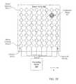
- FIG. 5Aillustrates a top-side view of one embodiment of a sensor array having a plurality of sensor elements for detecting a presence of a conductive object 303 on the sensor array 500 of a touch-sensor pad.
- Touch-sensor pad 220includes a sensor array 500 .
- Sensor array 500includes a plurality of rows 504 ( 1 )- 504 (N) and a plurality of columns 505 ( 1 )- 505 (M), where N is a positive integer value representative of the number of rows and M is a positive integer value representative of the number of columns.
- Each rowincludes a plurality of sensor elements 503 ( 1 )- 503 (K), where K is a positive integer value representative of the number of sensor elements in the row.
- Each columnincludes a plurality of sensor elements 501 ( 1 )- 501 (L), where L is a positive integer value representative of the number of sensor elements in the column.
- sensor arrayis an N ⁇ M sensor matrix.
- the N ⁇ M sensor matrixin conjunction with the processing device 210 , is configured to detect a position of a presence of the conductive object 303 in the x-, and y-directions.
- FIG. 5Billustrates a top-side view of one embodiment of a sensor array having a plurality of sensor elements for detecting a presence of a conductive object 303 on the sensor array 550 of a touch-sensor slider.
- Touch-sensor slider 230includes a sensor array 550 .
- Sensor array 550includes a plurality of columns 504 ( 1 )- 504 (M), where M is a positive integer value representative of the number of columns.
- Each columnincludes a plurality of sensor elements 501 ( 1 )- 501 (L), where L is a positive integer value representative of the number of sensor elements in the column. Accordingly, sensor array is a 1 ⁇ M sensor matrix.
- the 1 ⁇ M sensor matrixin conjunction with the processing device 210 , is configured to detect a position of a presence of the conductive object 303 in the x-direction. It should be noted that sensor array 500 may be configured to function as a touch-sensor slider 230 .
- Alternating columns in FIG. 5Acorrespond to x- and y-axis elements.
- the y-axis sensor elements 503 ( 1 )- 503 (K)are illustrated as black diamonds in FIG. 5A
- the x-axis sensor elements 501 ( 1 )- 501 (L)are illustrated as white diamonds in FIG. 5A and FIG. 5B .
- the columns and rowmay include vertical and horizontal bars (e.g., rectangular shaped bars); however, this design may include additional layers in the PCB to allow the vertical and horizontal bars to be positioned on the PCB so that they are not in contact with one another.
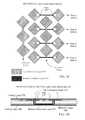
- FIGS. 5C and 5Dillustrate top-side and side views of one embodiment of a two-layer touch-sensor pad.
- Touch-sensor padas illustrated in FIGS. 5C and 5D , include the first two columns 505 ( 1 ) and 505 ( 2 ), and the first four rows 504 ( 1 )- 504 ( 4 ) of sensor array 500 .
- the sensor elements of the first column 501 ( 1 )are connected together in the top conductive layer 575 , illustrated as hashed diamond sensor elements and connections.
- the diamond sensor elements of each columnin effect, form a chain of elements.
- the sensor elements of the second column 501 ( 2 )are similarly connected in the top conductive layer 575 .
- the sensor elements of the first row 504 ( 1 )are connected together in the bottom conductive layer 575 using vias 577 , illustrated as black diamond sensor elements and connections.
- the diamond sensor elements of each rowin effect, form a chain of elements.
- the sensor elements of the second, third, and fourth rows 504 ( 2 )- 504 ( 4 )are similarly connected in the bottom conductive layer 576 .
- the top conductive layer 575includes the sensor elements for both the columns and the rows of the sensor array, as well as the connections between the sensor elements of the columns of the sensor array.
- the bottom conductive layer 576includes the conductive paths that connect the sensor elements of the rows that reside in the top conductive layer 575 .
- the conductive paths between the sensor elements of the rowsuse vias 577 to connect to one another in the bottom conductive layer 576 .
- Vias 577go from the top conductive layer 575 , through the dielectric layer 578 , to the bottom conductive layer 576 .
- Coating layers 579 and 589are applied to the surfaces opposite to the surfaces that are coupled to the dielectric layer 578 on both the top and bottom conductive layers 575 and 576 .
- the present embodimentsare not be limited to connecting the sensor elements of the rows using vias to the bottom conductive layer 576 , but may include connecting the sensor elements of the columns using vias to the bottom conductive layer 576 . Furthermore, the present embodiments are not limited two-layer configurations, but may include disposing the sensor elements on multiple layers, such as three- or four-layer configurations.
- pinsWhen pins are not being sensed (only one pin is sensed at a time), they are routed to ground.
- the sensing devicee.g., touch-sensor pad
- the exterior elementsBy surrounding the sensing device (e.g., touch-sensor pad) with a ground plane, the exterior elements have the same fringe capacitance to ground as the interior elements.
- an IC including the processing device 210may be directly placed on the non-sensor side of the PCB. This placement does not necessary have to be in the center.
- the processing device ICis not required to have a specific set of dimensions for a touch-sensor pad, nor a certain number of pins. Alternatively, the IC may be placed somewhere external to the PCB.
- FIG. 6Aillustrates one embodiment of a sensing device having three touch-sensor buttons.
- Sensing device 240 of FIG. 6Aincludes buttons 601 , 602 , and 603 . These three buttons may be used for user input using a conductive object, such as a finger.
- FIG. 6Billustrates one embodiment of the sensing device of FIG. 6A coupled to a processing device 210 .
- Processing device 210is used to detect whether a conductive object is present on either, or none, of the touch-sensor buttons 601 - 603 .
- the processing device 210may include capacitance sensors 201 ( 1 ) and 201 ( 2 ), which are coupled to buttons 601 - 603 .
- button 601is coupled to capacitance sensor 201 ( 1 )
- button 603is coupled to capacitance sensor 201 ( 2 )
- button 602is coupled to both capacitance sensor 201 ( 1 ) and 201 ( 2 ).
- Each of the conventional touch-sensor buttons 601 - 603may be made of a sensor element of conductive material, such as copper-clad.
- the conductive materialmay be formed in a circular shape (illustrated in FIGS. 6A-6D ), in a rectangular shape, or in a square shape (illustrated in FIGS. 7A and 7B ).
- the touch-sensor buttonsmay be capacitance sensor buttons, which may be used as non-contact switches. These switches, when protected by an insulating layer, offer resistance to severe environments.
- the sensing device of FIG. 6Bincludes two sensing areas 613 and 614 of conductive material that are electrically isolated.
- the sensing areas of conductive areaare used to make up the three buttons 601 - 603 .
- button 601includes a sensor element having a surface area of one conductive material (illustrated as white surface area of button 601 ).
- button 603includes a sensor element having a surface area of another conductive material (illustrated as hashed surface area of button 603 ).
- the conductive materialsmay be similar or dissimilar materials, but more importantly, are electrically isolated from one another.
- button 601is coupled to a first pin 609
- button 603is coupled to a second pin 610 of processing device 210 .
- Button 602includes a sensor element having a surface area of two conductive materials (illustrated as white and hashed surface areas of button 603 ) that are electrically isolated. A portion, first portion 604 , of the sensor element of button 602 is coupled to the conductive material of button 601 , and another portion, second portion 605 , is coupled to the conductive material of button 603 .
- first portion 604is coupled to the sensor element of button 601 using a conductive line 606
- second portion 605is coupled to the sensor element button 603 using a conductive line 607
- the conductive lines 606 and 607may be conductive traces printed on the surface of the PCB.
- conductive linesmay be conductive paths of conductive material that coupled the conductive material of the sensor elements and to the pins of the processing device 210 .
- the processing device 210scans the touch-sensor buttons 601 - 603 using the capacitance sensors 201 ( 1 ) and 201 ( 2 ), and measures the capacitance on the two sensing areas of conductive material that realize the touch-sensor buttons 601 - 603 .
- the processing deviceis operable to recognize a first button operation on the first sensor element, a second button operation on the second sensor element, and third button operation on the first and second portions of the third sensor element. Accordingly, the capacitance sensors of the processing device are not coupled to the touch-sensor buttons in a one-to-one configuration, like that of the conventional sensing device.
- the processing device 210may include only one capacitance sensor 201 that is coupled to a selection circuit.
- the selection circuitoperates to select one conductive path to scan and measure.
- the processing device 210includes two pins to couple to the two sensing areas of conductive material that make up the three or more buttons.
- the processing device 210may include only one pin and be coupled to a selection circuit that is external to the processing device that selects between the two sensing areas of conductive material.
- the processing device that is coupled to the sensing device of three or more touch-sensor buttonsincludes one more capacitance sensors coupled to the first and second sensor elements.
- the one or more capacitance sensorsare operable to measure capacitance on the three or more sensor elements. For example, if the capacitance variation ⁇ 1 , measured on the first pin 609 , is greater than zero, and the capacitance variation ⁇ 2 , measured on the second pin 610 is equal to approximately zero, then the first button 601 has been pressed. Similarly, if the capacitance variation ⁇ 1 , measured on the first pin 609 , is equal to the capacitance variation ⁇ 2 , measured on the second pin 610 , then the second button 602 has been pressed. If the capacitance variation ⁇ 1 , measured on the first pin 609 , is equal to approximately zero, and the capacitance variation ⁇ 2 , measured on the second pin 610 is greater than zero, then the third button 603 has been pressed.
- the one or more capacitance sensorsmay include a relaxation oscillator.
- the relaxation oscillatormay be similar to the relaxation oscillator described above, which includes a current source, a selection circuit, a comparator, and a reset switch.
- the relaxation oscillatormay be coupled to a digital counter that is operable to count at least one of a frequency or a period of a relaxation oscillator output received from the relaxation oscillator.
- the methodmay be performed by detecting a presence of a conductive object on a sensing device, and recognizing three or more button operations performed by the conductive object using two sensing areas of the sensing device.
- the operation of recognizing the three or more button operationsmay include recognizing a first button operation when the presence of the conductive object is detected on a first sensing area 613 of the two sensing areas of the sensing device, recognizing a second button operation when the presence of the conductive object is detected on a second sensing area 614 of the two sensing areas of the sensing device, and recognizing one or more button operations when the presence of the conductive object is detected on the first and second sensing areas 613 and 614 .
- the methodmay include the operation of determining a capacitance on each of the two sensing areas, and determining the three or more button operations based on the determined capacitance.
- the sensing areas 613 and 614may be scanned sequentially, or alternatively, may be scanned simultaneously by one or more capacitance sensors of the processing device 210 .
- the two sensing areasmay be used to realize three buttons, as illustrated in FIGS. 6A-6D .
- the two sensing areasmay be used to realize more than three button areas.
- the sensor elements of the touch-sensor buttonsmay be circular shaped, as illustrated in FIGS. 6A-6D .
- the sensor elementsmay have other shapes, such as rectangles, squares, ovals, hexagon, octagons, or the like.
- portions 613 and 614are substantially equal in surface area of the sensor element of button 602 . Alternatively, portions 613 and 614 are not equal in surface area. In one embodiment, the portions of sensor element of button 602 are semi-circularly shaped. Alternatively, the portions of the sensor element may have other shapes.
- FIG. 6Cillustrates another embodiment of a sensing device having three touch-sensor buttons.
- Sensing device 600includes three touch-sensor buttons that are similar to the touch-sensor buttons 601 - 603 of FIG. 6B , except the portions of the second sensor element of the second button 602 are dissimilarly shaped than the portions of FIG. 6B .
- First portion 604 of FIG. 6Chas a shape of two pie shapes.
- second portion 605 of FIG. 6Chas a shape of two pie shapes.
- the four pie shapesform a substantially circular shape for the sensor element.
- the two pie shapes of each portionare coupled together in a single layer, while the other two pie shapes are coupled together in a second conductive layer using vias, as described with respect to FIGS. 5C & 5D .
- the conductive material of one portionis coupled together using other methods known by those of ordinary skill in the art.
- conductive lines 606 and 607are conductive traces that couple the first and second portions 604 and 605 to the first and third sensor elements of button 601 and 603 , respectively.
- the conductive lines 607 and 608may be comprised of similar or dissimilar materials as the conductive material of the sensor elements. It should be noted that first portion 604 , sensor element of button 601 , and conductive line 606 are electrically isolated from second portion 605 , sensor element of button 603 , and conductive line 607 . Accordingly, the two sensing areas (e.g., 613 and 614 ) are comprised of these electrically isolated conductive materials.
- first and second portions 604 and 605each have a surface area that is substantially equal.
- the portionsmay have surface areas in other proportions.
- FIG. 6Dillustrates another embodiment of a sensing device having three touch-sensor buttons.
- Sensing device 650includes three touch-sensor buttons that are similar to the touch-sensor buttons 601 - 603 of FIG. 6B , except the portions of the second sensor element of the second button 602 are dissimilarly shaped than the portions of FIG. 6B .
- First portion 604 of FIG. 6Chas multiple arc shapes of conductive material that are electrically isolated from multiple arc shapes of another conductive material of second portion 605 . The multiple arc shapes of both the first and second portions 604 and 605 form a substantially circular shape for the sensor element.
- the multiple arc shapes of each portionare coupled together in a single layer, while the other two pie shapes are coupled together in a second conductive layer using vias, as described with respect to FIGS. 5C & 5D .
- the conductive material of one portionis coupled together using other methods known by those of ordinary skill in the art.
- conductive lines 606 and 607are conductive traces that couple the first and second portions 604 and 605 to the first and third sensor elements of button 601 and 603 , respectively.
- the conductive lines 607 and 608may be comprised of similar or dissimilar materials as the conductive material of the sensor elements. It should be noted that first portion 604 , sensor element of button 601 , and conductive line 606 are electrically isolated from second portion 605 , sensor element of button 603 , and conductive line 607 . Accordingly, the two sensing areas (e.g., 613 and 614 ) are comprised of these electrically isolated conductive materials.
- first and second portions 604 and 605each have a surface area that is substantially equal.
- the portionsmay have surface areas in other proportions.
- the shapes of the sensor elements and the portions of the sensor elementsare not limited to the shapes illustrated and described herein, but may include other shapes.
- FIGS. 7A and 7Binclude embodiments of rectangular and square shapes for the sensor elements and the portions of the sensor elements.
- the number of sensor elements in the sensing deviceis not limited to three, but may be greater than three.
- FIGS. 7A and 7Billustrate embodiments of four and five touch-sensor buttons; however, more sensor elements than five may also be used.
- FIG. 7Aillustrates another embodiment of a sensing device having four touch-sensor buttons.
- Sensing device 700includes four touch-sensor buttons 701 - 704 .
- Each of the conventional touch-sensor buttons 701 - 704may be made of a sensor element of conductive material, such as copper-clad.
- the sensor elements, in this embodimentare square shaped.
- the touch-sensor buttonsmay be capacitance sensor buttons, which may be used as non-contact switches.
- the sensing device 700 of FIG. 7Aincludes two sensing areas of conductive material that are electrically isolated.
- the sensing areas of conductive areaare used to make up the four buttons 701 - 704 .
- button 701includes a sensor element having a surface area of one conductive material (illustrated as white surface area of button 701 ).
- button 704includes a sensor element having a surface area of another conductive material (illustrated as hashed surface area of button 704 ).
- the conductive materialsmay be similar or dissimilar materials, but more importantly, are electrically isolated from one another.
- button 701is coupled to a first pin 609
- button 704is coupled to a second pin 610 of processing device 210 .
- Buttons 702 and 703include a sensor element having a surface area of two conductive materials (illustrated as white and hashed surface areas of buttons 702 and 703 ) that are electrically isolated. A portion, first portion 710 , of the sensor elements of buttons 702 and 703 is coupled to the conductive material of button 701 , and another portion, second portion 711 , is coupled to the conductive material of button 704 .
- first portion 710is coupled to the sensor element of button 701 using a conductive line 706
- second portion 711is coupled to the sensor element button 704 using a conductive line 707
- the conductive lines 706 and 707may be conductive traces printed on the surface of the PCB.
- conductive lines 706 and 707may be conductive paths of conductive material that coupled the conductive material of the sensor elements and to the pins of the processing device 210 .
- each sensor element of buttons 702 and 703comprises two surface areas, one surface area being the first portion 710 , and the other surface area being the second portion 711 .
- the surface areasmay be one solid shape, or alternatively, the surface areas may be interleaved sub-traces.
- the first conductive line 706is a first conductive trace
- the first conductive tracehas one or more sub-traces (e.g., 708 ( 1 )- 708 ( 7 ))
- the second conductive line 707is a second conductive trace that has one or more sub-traces (e.g., 709 ( 1 )- 709 ( 7 )).
- At least one sub-trace of the first conductive trace 706is interleaved with at least one sub-trace of the second conductive trace 707 .
- the sub-traces of the first and second conductive tracesare not interleaved.
- buttons 702 and 703each have a surface area ratio between the surface area of the first portion 710 and the second portion 711 .
- the surface area ratio of button 702is approximately 25% of the first portion 710 to approximately 75% of the second portion 711 (25/75).
- the surface area ratio of button 703is approximately 75% of the first portion 710 to approximately 25% of the second portion 711 (75/25).
- the surface area ratios of buttons 702 and 703may be switched in surface area ratios, e.g., 75/25 for button 702 and 25/75 for button 703 .
- button 702 and button 703may have other surface area ratios, ranging from 99/1 to 49/51, and vice versa.
- buttons 702 and 703each include seven sub-traces, sub-traces 708 ( 1 )- 708 ( 7 ) and sub-traces 709 ( 1 )- 709 ( 7 ).
- button 702includes four sub-traces 708 ( 1 )- 708 ( 4 ) of the first portion 710 , and three sub-traces 709 ( 1 )- 709 ( 3 ) of the second portion 711 .
- Button 703includes three sub-traces 708 ( 5 )- 708 ( 7 ) of the first portion 710 , and four sub-traces 709 ( 4 )- 709 ( 7 ) of the second portion 711 .
- the surface area ratio of button 702is 4/7 of the first portion 710 to 3/7 of the second portion 711
- the surface area ratio of button 703is 3/7 of the first portion 710 to 4/7 of the second portion 711 .
- other total number of sub-traces, and other combinations of sub-traces,may be used to form the different surface area ratios.
- FIG. 7Billustrates another embodiment of a sensing device having five touch-sensor buttons.
- Sensing device 750includes five touch-sensor buttons 701 - 705 .
- the touch-sensor buttons of sensing device 750are similar to those of sensing device 700 , expect there is one additional sensor element, and there are eight sub-traces per sensor element for buttons 702 - 704 , which consequently changes the surface area ratios.
- the sensing device 750 of FIG. 7Bincludes two sensing areas (illustrates a white and hashed surface areas) of conductive material that are electrically isolated.
- the sensing areas of conductive areaare used to make up the five buttons 701 - 705 .
- each sensor element of buttons 702 , 703 , and 704comprises two surface areas, one surface area being the first portion 710 , and the other surface area being the second portion 711 .
- the surface areasmay be one solid shape, or alternatively, the surface areas may be interleaved sub-traces.
- the first conductive line 706is a first conductive trace
- the first conductive tracehas twelve sub-traces 708 ( 1 )- 708 ( 12 )
- the second conductive line 707is a second conductive trace that has twelve sub-traces 709 ( 1 )- 709 ( 12 ). At least two sub-traces of both the first and second conductive traces are interleaved in each sensor element.
- the surface area ratio of button 702is approximately 6/8 of the first portion 710 to approximately 2/8 of the second portion 711 .
- the surface area ratio of button 703is approximately 4/8 (25%) of the first portion 710 to approximately 4/8 (50%) of the second portion 711 .
- the surface area ratio of button 704is approximately 2/8 of the first portion 710 to approximately 6/8 of the second portion 711 .
- the surface area ratio of button 702is approximately 25% of the first portion 710 to approximately 75% of the second portion 711 .
- the surface area ratio of button 703is approximately 50% of the first portion 710 to approximately 50% of the second portion 711 .
- the surface area ratio of button 704is approximately 75% of the first portion 710 to approximately 25% of the second portion 711 .
- the surface area ratio of button 702is approximately 33% of the first portion 710 to approximately 67% of the second portion 711 .
- the surface area ratio of button 703is approximately 50% of the first portion 710 to approximately 50% of the second portion 711 .
- the surface area ratio of button 704is approximately 67% of the first portion 710 to approximately 33% of the second portion 711 .
- the processing device 210can scan the touch-sensor buttons 701 - 704 of FIG. 7A (or the touch-sensor buttons 701 - 705 of FIG. 7B ) using one or more capacitance sensors, and measure the capacitance on the two sensing areas of conductive material that realize the touch-sensor buttons 701 - 704 (or 701 - 705 ). Accordingly, the processing device is operable to recognize a first button operation on the first sensor element, a second button operation on the second sensor element, and third and fourth button operations (or third, fourth, and fifth button operations) on the first and second portions of the third and fourth sensor elements (or third, fourth, and fifth sensor elements).
- the sensor elements that include the two portionsare illustrated and described as being inside or in between the two sensor elements that are coupled to the pins, the sensor elements that include the two portions may be disposed in other positions with respect to the other two sensor elements.
- Embodiments of the present inventioninclude various operations. These operations may be performed by hardware components, software, firmware, or a combination thereof.
- the term “coupled to”may mean coupled directly or indirectly through one or more intervening components. Any of the signals provided over various buses described herein may be time multiplexed with other signals and provided over one or more common buses. Additionally, the interconnection between circuit components or blocks may be shown as buses or as single signal lines. Each of the buses may alternatively be one or more single signal lines and each of the single signal lines may alternatively be buses.
- Certain embodimentsmay be implemented as a computer program product that may include instructions stored on a machine-readable medium. These instructions may be used to program a general-purpose or special-purpose processor to perform the described operations.
- a machine-readable mediumincludes any mechanism for storing or transmitting information in a form (e.g., software, processing application) readable by a machine (e.g., a computer).
- the machine-readable mediummay include, but is not limited to, magnetic storage medium (e.g., floppy diskette); optical storage medium (e.g., CD-ROM); magneto-optical storage medium; read-only memory (ROM); random-access memory (RAM); erasable programmable memory (e.g., EPROM and EEPROM); flash memory; electrical, optical, acoustical, or other form of propagated signal (e.g., carrier waves, infrared signals, digital signals, etc.); or another type of medium suitable for storing electronic instructions.
- magnetic storage mediume.g., floppy diskette
- optical storage mediume.g., CD-ROM
- magneto-optical storage mediume.g., magneto-optical storage medium
- ROMread-only memory
- RAMrandom-access memory
- EPROM and EEPROMerasable programmable memory
- flash memoryelectrical, optical, acoustical, or other form of propagated signal (e.g., carrier waves, in
- some embodimentsmay be practiced in distributed computing environments where the machine-readable medium is stored on and/or executed by more than one computer system.
- the information transferred between computer systemsmay either be pulled or pushed across the communication medium connecting the computer systems.
Landscapes
- Engineering & Computer Science (AREA)
- General Engineering & Computer Science (AREA)
- Theoretical Computer Science (AREA)
- Human Computer Interaction (AREA)
- Physics & Mathematics (AREA)
- General Physics & Mathematics (AREA)
- Electronic Switches (AREA)
- Position Input By Displaying (AREA)
- Measurement Of Resistance Or Impedance (AREA)
Abstract
Description
CdV=ICdt (1)
ΔC∝Δf, where (2)
Δf=fRO−fREF. (3)
Claims (20)
Priority Applications (3)
| Application Number | Priority Date | Filing Date | Title |
|---|---|---|---|
| US13/442,716US8519973B1 (en) | 2006-05-18 | 2012-04-09 | Apparatus and methods for detecting a conductive object at a location |
| US13/975,078US10209833B1 (en) | 2006-05-18 | 2013-08-23 | Apparatus and methods for detecting a conductive object at a location |
| US14/968,772US10248266B1 (en) | 2006-05-18 | 2015-12-14 | Two-pin buttons |
Applications Claiming Priority (3)
| Application Number | Priority Date | Filing Date | Title |
|---|---|---|---|
| US11/437,517US8004497B2 (en) | 2006-05-18 | 2006-05-18 | Two-pin buttons |
| US13/204,543US8174507B2 (en) | 2006-05-18 | 2011-08-05 | Apparatus and methods for detecting a conductive object at a location |
| US13/442,716US8519973B1 (en) | 2006-05-18 | 2012-04-09 | Apparatus and methods for detecting a conductive object at a location |
Related Parent Applications (1)
| Application Number | Title | Priority Date | Filing Date |
|---|---|---|---|
| US13/204,543ContinuationUS8174507B2 (en) | 2006-05-18 | 2011-08-05 | Apparatus and methods for detecting a conductive object at a location |
Related Child Applications (1)
| Application Number | Title | Priority Date | Filing Date |
|---|---|---|---|
| US13/975,078ContinuationUS10209833B1 (en) | 2006-05-18 | 2013-08-23 | Apparatus and methods for detecting a conductive object at a location |
Publications (1)
| Publication Number | Publication Date |
|---|---|
| US8519973B1true US8519973B1 (en) | 2013-08-27 |
Family
ID=38711538
Family Applications (5)
| Application Number | Title | Priority Date | Filing Date |
|---|---|---|---|
| US11/437,517Active2029-02-23US8004497B2 (en) | 2006-05-18 | 2006-05-18 | Two-pin buttons |
| US13/204,543ActiveUS8174507B2 (en) | 2006-05-18 | 2011-08-05 | Apparatus and methods for detecting a conductive object at a location |
| US13/442,716ActiveUS8519973B1 (en) | 2006-05-18 | 2012-04-09 | Apparatus and methods for detecting a conductive object at a location |
| US13/975,078ActiveUS10209833B1 (en) | 2006-05-18 | 2013-08-23 | Apparatus and methods for detecting a conductive object at a location |
| US14/968,772ActiveUS10248266B1 (en) | 2006-05-18 | 2015-12-14 | Two-pin buttons |
Family Applications Before (2)
| Application Number | Title | Priority Date | Filing Date |
|---|---|---|---|
| US11/437,517Active2029-02-23US8004497B2 (en) | 2006-05-18 | 2006-05-18 | Two-pin buttons |
| US13/204,543ActiveUS8174507B2 (en) | 2006-05-18 | 2011-08-05 | Apparatus and methods for detecting a conductive object at a location |
Family Applications After (2)
| Application Number | Title | Priority Date | Filing Date |
|---|---|---|---|
| US13/975,078ActiveUS10209833B1 (en) | 2006-05-18 | 2013-08-23 | Apparatus and methods for detecting a conductive object at a location |
| US14/968,772ActiveUS10248266B1 (en) | 2006-05-18 | 2015-12-14 | Two-pin buttons |
Country Status (1)
| Country | Link |
|---|---|
| US (5) | US8004497B2 (en) |
Cited By (6)
| Publication number | Priority date | Publication date | Assignee | Title |
|---|---|---|---|---|
| US8872526B1 (en)* | 2013-09-10 | 2014-10-28 | Cypress Semiconductor Corporation | Interleaving sense elements of a capacitive-sense array |
| US8903679B2 (en) | 2011-09-23 | 2014-12-02 | Cypress Semiconductor Corporation | Accuracy in a capacitive sense array |
| US9304643B2 (en) | 2014-06-24 | 2016-04-05 | Synaptics Incorporated | Classifying input objects interacting with a capacitive button |
| US9495050B1 (en) | 2013-09-10 | 2016-11-15 | Monterey Research, Llc | Sensor pattern with signal-spreading electrodes |
| US9612265B1 (en) | 2011-09-23 | 2017-04-04 | Cypress Semiconductor Corporation | Methods and apparatus to detect a conductive object |
| US10268308B2 (en) | 2015-11-06 | 2019-04-23 | Samsung Electronics Co., Ltd | Input processing method and device |
Families Citing this family (96)
| Publication number | Priority date | Publication date | Assignee | Title |
|---|---|---|---|---|
| US8040142B1 (en) | 2006-03-31 | 2011-10-18 | Cypress Semiconductor Corporation | Touch detection techniques for capacitive touch sense systems |
| US8004497B2 (en) | 2006-05-18 | 2011-08-23 | Cypress Semiconductor Corporation | Two-pin buttons |
| US8547114B2 (en) | 2006-11-14 | 2013-10-01 | Cypress Semiconductor Corporation | Capacitance to code converter with sigma-delta modulator |
| US8159462B1 (en)* | 2006-11-15 | 2012-04-17 | Cypress Semiconductor Corporation | Reference voltage offset for capacitive touch-sensor measurement |
| US8058937B2 (en) | 2007-01-30 | 2011-11-15 | Cypress Semiconductor Corporation | Setting a discharge rate and a charge rate of a relaxation oscillator circuit |
| US20080198145A1 (en)* | 2007-02-20 | 2008-08-21 | Knowles Terrence J | Acoustic wave touch actuated system |
| TW200842681A (en) | 2007-04-27 | 2008-11-01 | Tpk Touch Solutions Inc | Touch pattern structure of a capacitive touch panel |
| US9500686B1 (en) | 2007-06-29 | 2016-11-22 | Cypress Semiconductor Corporation | Capacitance measurement system and methods |
| US8169238B1 (en) | 2007-07-03 | 2012-05-01 | Cypress Semiconductor Corporation | Capacitance to frequency converter |
| US8570053B1 (en) | 2007-07-03 | 2013-10-29 | Cypress Semiconductor Corporation | Capacitive field sensor with sigma-delta modulator |
| US8605050B2 (en) | 2007-08-21 | 2013-12-10 | Tpk Touch Solutions (Xiamen) Inc. | Conductor pattern structure of capacitive touch panel |
| WO2009058745A2 (en) | 2007-10-28 | 2009-05-07 | Synaptics Incorporated | Determining actuation of multi-sensor electrode capacitive buttons |
| TWI374379B (en) | 2007-12-24 | 2012-10-11 | Wintek Corp | Transparent capacitive touch panel and manufacturing method thereof |
| US8525798B2 (en) | 2008-01-28 | 2013-09-03 | Cypress Semiconductor Corporation | Touch sensing |
| US8319505B1 (en) | 2008-10-24 | 2012-11-27 | Cypress Semiconductor Corporation | Methods and circuits for measuring mutual and self capacitance |
| US8358142B2 (en) | 2008-02-27 | 2013-01-22 | Cypress Semiconductor Corporation | Methods and circuits for measuring mutual and self capacitance |
| US9104273B1 (en) | 2008-02-29 | 2015-08-11 | Cypress Semiconductor Corporation | Multi-touch sensing method |
| US8228306B2 (en) | 2008-07-23 | 2012-07-24 | Flextronics Ap, Llc | Integration design for capacitive touch panels and liquid crystal displays |
| US9128568B2 (en) | 2008-07-30 | 2015-09-08 | New Vision Display (Shenzhen) Co., Limited | Capacitive touch panel with FPC connector electrically coupled to conductive traces of face-to-face ITO pattern structure in single plane |
| US8492665B1 (en)* | 2008-08-11 | 2013-07-23 | Jiandong Yang | Apparatus and methods for capacitive sensing and capacitance measuring |
| US8321174B1 (en) | 2008-09-26 | 2012-11-27 | Cypress Semiconductor Corporation | System and method to measure capacitance of capacitive sensor array |
| KR100971501B1 (en)* | 2008-10-24 | 2010-07-21 | 주식회사 애트랩 | Contact sensor device |
| US8209861B2 (en) | 2008-12-05 | 2012-07-03 | Flextronics Ap, Llc | Method for manufacturing a touch screen sensor assembly |
| US8669944B2 (en)* | 2008-12-15 | 2014-03-11 | Sony Corporation | Touch sensitive displays with layers of sensor plates providing capacitance based proximity sensing and related touch panels |
| US8274486B2 (en) | 2008-12-22 | 2012-09-25 | Flextronics Ap, Llc | Diamond pattern on a single layer |
| WO2010105507A1 (en) | 2009-03-20 | 2010-09-23 | 宸鸿科技(厦门)有限公司 | Capacitive touch circuit pattern and manufacturing method thereof |
| US9024907B2 (en) | 2009-04-03 | 2015-05-05 | Synaptics Incorporated | Input device with capacitive force sensor and method for constructing the same |
| US8294601B2 (en)* | 2009-11-13 | 2012-10-23 | Research In Motion Limited | Detection of intended key activation on a mobile device |
| JP5540797B2 (en)* | 2010-03-19 | 2014-07-02 | ソニー株式会社 | Sensor device and display device |
| US9285929B2 (en) | 2010-03-30 | 2016-03-15 | New Vision Display (Shenzhen) Co., Limited | Touchscreen system with simplified mechanical touchscreen design using capacitance and acoustic sensing technologies, and method therefor |
| TWI420364B (en)* | 2010-05-03 | 2013-12-21 | Htc Corp | Touch-controlled electronic apparatus and related assembly method |
| US9057653B2 (en)* | 2010-05-11 | 2015-06-16 | Synaptics Incorporated | Input device with force sensing |
| TW201235901A (en)* | 2011-02-21 | 2012-09-01 | Wistron Corp | Touch control device |
| FI122844B (en)* | 2011-04-21 | 2012-07-31 | Kone Corp | INVITATION EQUIPMENT AND METHOD FOR GIVING A LIFT CALL |
| US9557857B2 (en) | 2011-04-26 | 2017-01-31 | Synaptics Incorporated | Input device with force sensing and haptic response |
| CN102866794A (en) | 2011-06-15 | 2013-01-09 | 宸鸿光电科技股份有限公司 | Touch sensing layer and manufacturing method thereof |
| US9748952B2 (en) | 2011-09-21 | 2017-08-29 | Synaptics Incorporated | Input device with integrated deformable electrode structure for force sensing |
| US9041418B2 (en) | 2011-10-25 | 2015-05-26 | Synaptics Incorporated | Input device with force sensing |
| TWM426082U (en)* | 2011-11-29 | 2012-04-01 | Henghao Technology Co Ltd | Touch panel and touch display panel using the same |
| JP6052914B2 (en) | 2012-01-12 | 2016-12-27 | シナプティクス インコーポレイテッド | Single-layer capacitive imaging sensor |
| US8525955B2 (en) | 2012-01-31 | 2013-09-03 | Multek Display (Hong Kong) Limited | Heater for liquid crystal display |
| US8436627B1 (en) | 2012-03-16 | 2013-05-07 | Cypress Semiconductor Corporation | Serpentine touch sensor pattern |
| US9806713B2 (en) | 2012-05-15 | 2017-10-31 | Thomson Licensing | Capacitive touch button with guard |
| US8773386B2 (en)* | 2012-08-09 | 2014-07-08 | Cypress Semiconductor Corporation | Methods and apparatus to scan a targeted portion of an input device to detect a presence |
| US9465446B2 (en) | 2013-03-14 | 2016-10-11 | Blackberry Limited | Electronic device including mechanical keyboard having touch sensors for detecting touches and actuation of mechanical keys |
| US9552089B2 (en) | 2013-08-07 | 2017-01-24 | Synaptics Incorporated | Capacitive sensing using a matrix electrode pattern |
| US20150091842A1 (en) | 2013-09-30 | 2015-04-02 | Synaptics Incorporated | Matrix sensor for image touch sensing |
| US9298325B2 (en) | 2013-09-30 | 2016-03-29 | Synaptics Incorporated | Processing system for a capacitive sensing device |
| US10042489B2 (en) | 2013-09-30 | 2018-08-07 | Synaptics Incorporated | Matrix sensor for image touch sensing |
| US9459367B2 (en) | 2013-10-02 | 2016-10-04 | Synaptics Incorporated | Capacitive sensor driving technique that enables hybrid sensing or equalization |
| US9274662B2 (en) | 2013-10-18 | 2016-03-01 | Synaptics Incorporated | Sensor matrix pad for performing multiple capacitive sensing techniques |
| US9081457B2 (en) | 2013-10-30 | 2015-07-14 | Synaptics Incorporated | Single-layer muti-touch capacitive imaging sensor |
| TWI528256B (en)* | 2014-01-07 | 2016-04-01 | 緯創資通股份有限公司 | Touch emulator |
| US9798429B2 (en) | 2014-02-28 | 2017-10-24 | Synaptics Incorporated | Guard electrodes in a sensing stack |
| US10133421B2 (en) | 2014-04-02 | 2018-11-20 | Synaptics Incorporated | Display stackups for matrix sensor |
| US9927832B2 (en) | 2014-04-25 | 2018-03-27 | Synaptics Incorporated | Input device having a reduced border region |
| US9690397B2 (en) | 2014-05-20 | 2017-06-27 | Synaptics Incorporated | System and method for detecting an active pen with a matrix sensor |
| TWI543053B (en)* | 2014-06-19 | 2016-07-21 | 晨星半導體股份有限公司 | Touch control device |
| US10175827B2 (en) | 2014-12-23 | 2019-01-08 | Synaptics Incorporated | Detecting an active pen using a capacitive sensing device |
| US10795471B2 (en) | 2015-01-05 | 2020-10-06 | Synaptics Incorporated | Modulating a reference voltage to perform capacitive sensing |
| US9939972B2 (en) | 2015-04-06 | 2018-04-10 | Synaptics Incorporated | Matrix sensor with via routing |
| US10126861B2 (en) | 2015-05-08 | 2018-11-13 | Synaptics Incorporated | Force sensor substrate |
| USD776664S1 (en)* | 2015-05-20 | 2017-01-17 | Chaya Coleena Hendrick | Smart card |
| US9715304B2 (en) | 2015-06-30 | 2017-07-25 | Synaptics Incorporated | Regular via pattern for sensor-based input device |
| US9720541B2 (en) | 2015-06-30 | 2017-08-01 | Synaptics Incorporated | Arrangement of sensor pads and display driver pads for input device |
| US10095948B2 (en) | 2015-06-30 | 2018-10-09 | Synaptics Incorporated | Modulation scheme for fingerprint sensing |
| CN205028263U (en) | 2015-09-07 | 2016-02-10 | 辛纳普蒂克斯公司 | Capacitance sensor |
| US9971463B2 (en)* | 2015-09-29 | 2018-05-15 | Synaptics Incorporated | Row-based sensing on matrix pad sensors |
| US10037112B2 (en) | 2015-09-30 | 2018-07-31 | Synaptics Incorporated | Sensing an active device'S transmission using timing interleaved with display updates |
| US10067587B2 (en) | 2015-12-29 | 2018-09-04 | Synaptics Incorporated | Routing conductors in an integrated display device and sensing device |
| CN106933400B (en) | 2015-12-31 | 2021-10-29 | 辛纳普蒂克斯公司 | Single-layer sensor pattern and sensing method |
| US10452211B2 (en) | 2016-05-27 | 2019-10-22 | Synaptics Incorporated | Force sensor with uniform response in an axis |
| US10151616B1 (en)* | 2017-11-28 | 2018-12-11 | Semiconductor Components Industries, Llc | Flowable material level sensing with shaped electrodes |
| US10236900B1 (en)* | 2017-12-11 | 2019-03-19 | Texas Instruments Incorporated | Capacitive mismatch measurement |
| US11092657B2 (en) | 2018-03-29 | 2021-08-17 | Cirrus Logic, Inc. | Compensation of changes in a resonant phase sensing system including a resistive-inductive-capacitive sensor |
| US10642435B2 (en) | 2018-03-29 | 2020-05-05 | Cirrus Logic, Inc. | False triggering prevention in a resonant phase sensing system |
| US11537242B2 (en) | 2018-03-29 | 2022-12-27 | Cirrus Logic, Inc. | Q-factor enhancement in resonant phase sensing of resistive-inductive-capacitive sensors |
| US12295102B1 (en) | 2018-03-29 | 2025-05-06 | Cirrus Logic Inc. | Far field interference cancellation for resistive-inductive-capacitive sensors |
| US12130159B2 (en) | 2018-08-22 | 2024-10-29 | Cirrus Logic Inc. | Detecting and adapting to changes in a resonant phase sensing system having a resistive-inductive-capacitive sensor |
| US11536758B2 (en) | 2019-02-26 | 2022-12-27 | Cirrus Logic, Inc. | Single-capacitor inductive sense systems |
| US11402946B2 (en) | 2019-02-26 | 2022-08-02 | Cirrus Logic, Inc. | Multi-chip synchronization in sensor applications |
| US10948313B2 (en) | 2019-02-26 | 2021-03-16 | Cirrus Logic, Inc. | Spread spectrum sensor scanning using resistive-inductive-capacitive sensors |
| CN110187264B (en)* | 2019-05-29 | 2021-08-20 | 西安西电电气研究院有限责任公司 | Method and device for determining mechanical degeneration of high voltage circuit breaker |
| US11171641B2 (en)* | 2019-06-03 | 2021-11-09 | Cirrus Logic, Inc. | Compensation for air gap changes and temperature changes in a resonant phase detector |
| US10790824B1 (en)* | 2019-07-03 | 2020-09-29 | Samsung Electro-Mechanics Co., Ltd. | Switching operation sensing apparatus with touch input member identification |
| KR102149385B1 (en)* | 2019-09-20 | 2020-08-31 | 삼성전기주식회사 | Force sensing device with slide detecting and electrical device |
| US11579030B2 (en) | 2020-06-18 | 2023-02-14 | Cirrus Logic, Inc. | Baseline estimation for sensor system |
| US11868540B2 (en) | 2020-06-25 | 2024-01-09 | Cirrus Logic Inc. | Determination of resonant frequency and quality factor for a sensor system |
| US11835410B2 (en) | 2020-06-25 | 2023-12-05 | Cirrus Logic Inc. | Determination of resonant frequency and quality factor for a sensor system |
| US11619519B2 (en) | 2021-02-08 | 2023-04-04 | Cirrus Logic, Inc. | Predictive sensor tracking optimization in multi-sensor sensing applications |
| US11808669B2 (en) | 2021-03-29 | 2023-11-07 | Cirrus Logic Inc. | Gain and mismatch calibration for a phase detector used in an inductive sensor |
| US11821761B2 (en) | 2021-03-29 | 2023-11-21 | Cirrus Logic Inc. | Maximizing dynamic range in resonant sensing |
| US11507199B2 (en) | 2021-03-30 | 2022-11-22 | Cirrus Logic, Inc. | Pseudo-differential phase measurement and quality factor compensation |
| US11474650B1 (en)* | 2021-05-03 | 2022-10-18 | Image Match Design Inc. | Fingerprint recognition device and fingerprint recognition method thereof |
| US11979115B2 (en) | 2021-11-30 | 2024-05-07 | Cirrus Logic Inc. | Modulator feedforward compensation |
| US11854738B2 (en) | 2021-12-02 | 2023-12-26 | Cirrus Logic Inc. | Slew control for variable load pulse-width modulation driver and load sensing |
Citations (127)
| Publication number | Priority date | Publication date | Assignee | Title |
|---|---|---|---|---|
| US3979745A (en) | 1974-02-22 | 1976-09-07 | Westronics, Inc. | System and method for linearizing analog measurements during analog-to-digital conversion |
| US4039940A (en) | 1976-07-30 | 1977-08-02 | General Electric Company | Capacitance sensor |
| US4113378A (en) | 1977-03-02 | 1978-09-12 | Itek Corporation | Linear exposure control system |
| US4145748A (en) | 1977-12-23 | 1979-03-20 | General Electric Company | Self-optimizing touch pad sensor circuit |
| US4193063A (en) | 1978-05-15 | 1980-03-11 | Leeds & Northrup Company | Differential capacitance measuring circuit |
| US4238711A (en) | 1979-08-20 | 1980-12-09 | General Electric Company | Circuit for selective individual operation of multiple arc discharge lamps |
| US4264903A (en) | 1978-06-12 | 1981-04-28 | General Electric Company | Capacitive touch control and display |
| US4266144A (en) | 1979-05-14 | 1981-05-05 | Emhart Industries, Inc. | Detection means for multiple capacitive sensing devices |
| US4292604A (en) | 1979-08-20 | 1981-09-29 | Bell Telephone Laboratories, Incorporated | Relaxation oscillator with plural constant current sources |
| US4305135A (en) | 1979-07-30 | 1981-12-08 | International Business Machines Corp. | Program controlled capacitive keyboard variable threshold sensing system |
| US4586260A (en) | 1984-05-29 | 1986-05-06 | The L. S. Starrett Company | Capacitive displacement measuring instrument |
| US4614937A (en) | 1982-01-29 | 1986-09-30 | Commissariat A L'energie Atomique | Capacitive keyboard structure |
| US4728932A (en) | 1986-07-25 | 1988-03-01 | Honeywell Inc. | Detector for capacitive sensing devices |
| US4736191A (en) | 1985-08-02 | 1988-04-05 | Karl E. Matzke | Touch activated control method and apparatus |
| US4825147A (en) | 1988-09-14 | 1989-04-25 | Sencore, Inc. | Capacitance measuring method and apparatus |
| US4831325A (en) | 1987-04-01 | 1989-05-16 | General Signal Corporation | Capacitance measuring circuit |
| US5008497A (en) | 1990-03-22 | 1991-04-16 | Asher David J | Touch controller |
| US5214388A (en) | 1992-05-28 | 1993-05-25 | The United States Of America As Represented By The Administrator Of The National Aeronautics And Space Administration | Phase discriminating capacitive array sensor system |
| US5237879A (en) | 1991-10-11 | 1993-08-24 | At&T Bell Laboratories | Apparatus for dynamically varying the resolution of a tactile sensor array |
| US5305017A (en) | 1989-08-16 | 1994-04-19 | Gerpheide George E | Methods and apparatus for data input |
| US5323158A (en) | 1993-04-06 | 1994-06-21 | Analog Devices, Inc. | Switched capacitor one-bit digital-to-analog converter |
| US5373245A (en) | 1993-07-12 | 1994-12-13 | The United States Of America As Represented By The Administrator Of The National Aeronautics And Space Administration | Capaciflector camera |
| US5386219A (en) | 1991-10-16 | 1995-01-31 | International Business Machines Corp. | Touch overlay for improved touch sensitivity |
| US5463388A (en) | 1993-01-29 | 1995-10-31 | At&T Ipm Corp. | Computer mouse or keyboard input device utilizing capacitive sensors |
| US5518078A (en)* | 1991-11-08 | 1996-05-21 | Sharp Kabushiki Kaisha | Coordinates input device |
| US5541580A (en) | 1993-11-18 | 1996-07-30 | Motorola, Inc. | Body detector |
| US5670915A (en) | 1996-05-24 | 1997-09-23 | Microchip Technology Incorporated | Accurate RC oscillator having peak - to - peak voltage control |
| US5760852A (en) | 1995-11-03 | 1998-06-02 | Hughes Electronics Corporation | Laser-hardened eye protection goggles |
| US5801340A (en) | 1995-06-29 | 1998-09-01 | Invotronics Manufacturing | Proximity sensor |
| US5920309A (en) | 1996-01-04 | 1999-07-06 | Logitech, Inc. | Touch sensing method and apparatus |
| US5942733A (en) | 1992-06-08 | 1999-08-24 | Synaptics, Inc. | Stylus input capacitive touchpad sensor |
| US6037929A (en) | 1996-08-30 | 2000-03-14 | Alps Electric Co., Ltd. | Coordinate input system and method of controlling same |
| US6060957A (en) | 1998-12-08 | 2000-05-09 | Stmicroelectronics S.A. | Relaxation oscillator with low phase noise |
| US6145850A (en) | 1998-10-24 | 2000-11-14 | Smw Autoblok Spannsysteme Gmbh | Diaphragm chuck |
| US6184871B1 (en) | 1996-10-25 | 2001-02-06 | Asulab S.A. | Identification device of a manual action on a surface, in particular for a timeplace |
| US6188391B1 (en) | 1998-07-09 | 2001-02-13 | Synaptics, Inc. | Two-layer capacitive touchpad and method of making same |
| US6191723B1 (en) | 1999-07-22 | 2001-02-20 | Fluke Corporation | Fast capacitance measurement |
| US6297811B1 (en) | 1999-06-02 | 2001-10-02 | Elo Touchsystems, Inc. | Projective capacitive touchscreen |
| US6353200B2 (en) | 1998-05-04 | 2002-03-05 | Inocon Technologie Gesellschaft M.B.H. | Method for the partial fusion of objects |
| US6366099B1 (en) | 1999-12-21 | 2002-04-02 | Conrad Technologies, Inc. | Differential capacitance sampler |
| US6377129B1 (en) | 1999-04-30 | 2002-04-23 | Conexant Systems, Inc. | Programmable relaxation oscillator |
| US6380931B1 (en) | 1992-06-08 | 2002-04-30 | Synaptics Incorporated | Object position detector with edge motion feature and gesture recognition |
| US6448911B1 (en) | 2001-07-30 | 2002-09-10 | Cirrus Logic, Inc. | Circuits and methods for linearizing capacitor calibration and systems using the same |
| US6490203B1 (en) | 2001-05-24 | 2002-12-03 | Edn Silicon Devices, Inc. | Sensing scheme of flash EEPROM |
| US6535200B2 (en) | 1999-01-25 | 2003-03-18 | Harald Philipp | Capacitive position sensor |
| US20030091220A1 (en) | 2001-11-13 | 2003-05-15 | Toko, Inc. | Capacitive sensor device |
| US6577140B1 (en) | 1999-01-27 | 2003-06-10 | Richard A. Wenman | Method and device for measuring the acidity or basicity of insulating fluids, particularly mineral and synthetic oils |
| US6583632B2 (en) | 1998-07-23 | 2003-06-24 | Micronas Gmbh | Method of determining very small capacitances |
| US6700392B2 (en) | 2001-02-02 | 2004-03-02 | Wayne C. Haase | Digital measurement circuit and system using a grounded capacitive sensor |
| US6781577B2 (en) | 2000-07-04 | 2004-08-24 | Alps Electric Co., Ltd. | Capacitive sensor-based input device |
| US20040178989A1 (en) | 2002-10-20 | 2004-09-16 | Shahoian Erik J. | System and method for providing rotational haptic feedback |
| US6806693B1 (en) | 2003-04-14 | 2004-10-19 | National Semiconductor Corporation | Method and system for improving quiescent currents at low output current levels |
| US20040217945A1 (en) | 2001-08-22 | 2004-11-04 | Saburo Miyamoto | Touch sensor, display with touch sensor, and method for generating position data |
| US6825673B1 (en) | 2000-05-19 | 2004-11-30 | Oht Inc. | Method and apparatus for circuit board continuity test, tool for continuity test, and recording medium |
| US20040239616A1 (en)* | 2003-05-28 | 2004-12-02 | Collins Ryan V. | Methods and apparatus for receiving user input via time domain reflectometry |
| US6838887B2 (en) | 2001-02-09 | 2005-01-04 | Georgia-Pacific Corporation | Proximity detection circuit and method of detecting small capacitance changes |
| US20050031175A1 (en) | 2003-07-28 | 2005-02-10 | Seiko Epson Corporation | Input device, electronic apparatus, and method for driving input device |
| US6859159B2 (en) | 2002-06-18 | 2005-02-22 | Analog Devices, Inc. | Switched-capacitor structures with enhanced isolation |
| US20050052429A1 (en) | 2003-08-21 | 2005-03-10 | Harald Philipp | Capacitive position sensor |
| US6879930B2 (en) | 2001-03-30 | 2005-04-12 | Microsoft Corporation | Capacitance touch slider |
| US6882338B2 (en) | 2002-08-16 | 2005-04-19 | Leapfrog Enterprises, Inc. | Electrographic position location apparatus |
| US6888536B2 (en) | 1998-01-26 | 2005-05-03 | The University Of Delaware | Method and apparatus for integrating manual input |
| US6891531B2 (en) | 2002-07-05 | 2005-05-10 | Sentelic Corporation | Sensing an object with a plurality of conductors |
| US6914547B1 (en) | 2004-05-04 | 2005-07-05 | Analog Devices, Inc. | Triple resistor string DAC architecture |
| US20050159126A1 (en) | 2004-01-16 | 2005-07-21 | Chun-Hsiung Wang | Apparatus and method of interruptible analog input |
| US20050179672A1 (en) | 2004-02-17 | 2005-08-18 | Yen-Chang Chiu | Simplified capacitive touchpad and method thereof |
| US6933873B1 (en) | 2000-11-01 | 2005-08-23 | Analog Devices, Inc. | PWM-based measurement interface for a micro-machined electrostatic actuator |
| US6940291B1 (en) | 2001-01-02 | 2005-09-06 | Irobot Corporation | Capacitive sensor systems and methods with increased resolution and automatic calibration |
| US6946853B2 (en) | 2001-06-08 | 2005-09-20 | Intier Automotive Closures Inc. | Non-contact proximity sensor |
| US6958594B2 (en) | 2004-01-21 | 2005-10-25 | Analog Devices, Inc. | Switched noise filter circuit for a DC-DC converter |
| US6970120B1 (en) | 2004-06-12 | 2005-11-29 | Nordic Semiconductor Asa | Method and apparatus for start-up of analog-to-digital converters |
| US6970126B1 (en) | 2004-06-25 | 2005-11-29 | Analog Devices, Inc. | Variable capacitance switched capacitor input system and method |
| US20060016800A1 (en)* | 2004-07-20 | 2006-01-26 | Massachusetts Institute Of Technology | Continuous capacitive slider controller for a smooth surfaced cooktop |
| US20060038793A1 (en) | 2003-10-08 | 2006-02-23 | Harald Philipp | Touch Sensitive Control Panel |
| US7006078B2 (en) | 2002-05-07 | 2006-02-28 | Mcquint, Inc. | Apparatus and method for sensing the degree and touch strength of a human body on a sensor |
| US7032051B2 (en) | 2000-12-11 | 2006-04-18 | Linear Technology Corp. | Methods and circuitry for interconnecting data and clock busses of live backplane circuitry and input/output card circuitry, and methods and circuitry for isolating capacitanes of a live backplane from the capacitanes of at least one input/output card |
| US7031886B1 (en) | 2004-12-14 | 2006-04-18 | Synaptics Incorporated | Methods and systems for detecting noise in a position sensor using minor shifts in sensing frequency |
| US20060097992A1 (en)* | 2004-10-25 | 2006-05-11 | Motorola, Inc. | Apparatus and method of determining a user selection in a user interface |
| US7046230B2 (en) | 2001-10-22 | 2006-05-16 | Apple Computer, Inc. | Touch pad handheld device |
| US20060131159A1 (en) | 2004-12-17 | 2006-06-22 | Diehl Ako Stiftung & Co., Kg | Capacitive touch switch |
| US7068039B2 (en) | 2004-04-28 | 2006-06-27 | Agilent Technologies, Inc. | Test structure embedded in a shipping and handling cover for integrated circuit sockets and method for testing integrated circuit sockets and circuit assemblies utilizing same |
| US7075316B2 (en) | 2003-10-02 | 2006-07-11 | Alps Electric Co., Ltd. | Capacitance detector circuit, capacitance detection method, and fingerprint sensor using the same |
| US7078916B2 (en) | 2004-04-06 | 2006-07-18 | Analog Devices, Inc. | Linearity enhancement for capacitive sensors |
| US7098675B2 (en) | 2004-03-30 | 2006-08-29 | Aisin Seiki Kabushiki Kaisha | Capacitance change detection device |
| US20060197750A1 (en) | 2005-03-04 | 2006-09-07 | Apple Computer, Inc. | Hand held electronic device with multiple touch sensing devices |
| US20060227117A1 (en)* | 2005-04-07 | 2006-10-12 | Microsoft Corporation | Circular touch sensor |
| US20060232559A1 (en) | 2005-04-19 | 2006-10-19 | Yung-Lieh Chien | Capacitive touchpad with physical key function |
| US7129935B2 (en) | 2003-06-02 | 2006-10-31 | Synaptics Incorporated | Sensor patterns for a capacitive sensing apparatus |
| US20060262101A1 (en) | 2005-02-10 | 2006-11-23 | Layton Michael D | Expanded electrode grid of a capacitance sensitive touchpad by using demultiplexing of signals to the grid as controlled by binary patterns from a touch sensor circuit |
| US7148704B2 (en) | 2002-10-31 | 2006-12-12 | Harald Philipp | Charge transfer capacitive position sensor |
| US20070076897A1 (en) | 2005-09-30 | 2007-04-05 | Harald Philipp | Headsets and Headset Power Management |
| US7235983B2 (en) | 2005-03-09 | 2007-06-26 | Analog Devices, Inc. | One terminal capacitor interface circuit |
| US7253643B1 (en)* | 2006-07-19 | 2007-08-07 | Cypress Semiconductor Corporation | Uninterrupted radial capacitive sense interface |
| US7262609B2 (en) | 2005-06-03 | 2007-08-28 | Synaptics Incorporated | Methods and systems for guarding a charge transfer capacitance sensor for proximity detection |
| US20070247443A1 (en) | 2006-04-25 | 2007-10-25 | Harald Philipp | Hybrid Capacitive Touch Screen Element |
| US7288946B2 (en) | 2005-06-03 | 2007-10-30 | Synaptics Incorporated | Methods and systems for detecting a capacitance using sigma-delta measurement techniques |
| US20070257894A1 (en) | 2006-05-05 | 2007-11-08 | Harald Philipp | Touch Screen Element |
| US20070268265A1 (en)* | 2006-05-18 | 2007-11-22 | Cypress Semiconductor Corporation | Two-pin buttons |
| US7301350B2 (en) | 2005-06-03 | 2007-11-27 | Synaptics Incorporated | Methods and systems for detecting a capacitance using sigma-delta measurement techniques |
| US7307485B1 (en) | 2005-11-14 | 2007-12-11 | Cypress Semiconductor Corporation | Capacitance sensor using relaxation oscillators |
| US20070291013A1 (en)* | 2006-06-20 | 2007-12-20 | Lg Electronics Inc. | Touchpad including non-overlapping sensors |
| US20070296709A1 (en) | 2006-06-27 | 2007-12-27 | Cypress Semiconductor Corporation | Apparatus and method for detecting multiple buttons with one pin |
| US20070296694A1 (en) | 2006-06-26 | 2007-12-27 | Samsung Electronics Co., Ltd. | Input device with display buttons and portable electronic device having the same |
| US20080007534A1 (en) | 2006-07-10 | 2008-01-10 | Cypress Semiconductor Corporation | Touch-sensor with shared capacitive sensors |
| US7323886B2 (en) | 2004-08-16 | 2008-01-29 | Ying Lau Lee | Linear capacitance measurement and touchless switch |
| US20080024455A1 (en) | 2006-07-25 | 2008-01-31 | Lee Mark R | Technique for increasing the sensitivity of capacitive sensor arrays |
| US20080036473A1 (en) | 2006-08-09 | 2008-02-14 | Jansson Hakan K | Dual-slope charging relaxation oscillator for measuring capacitance |
| US20080068100A1 (en) | 2006-09-12 | 2008-03-20 | Goodnow Kenneth J | Power management architecture and method of modulating oscillator frequency based on voltage supply |
| US7359816B2 (en) | 2005-05-25 | 2008-04-15 | Analog Devices, Inc. | Sensor calibration method and apparatus |
| US20080111714A1 (en)* | 2006-11-14 | 2008-05-15 | Viktor Kremin | Capacitance to code converter with sigma-delta modulator |
| US7375535B1 (en) | 2005-09-19 | 2008-05-20 | Cypress Semiconductor Corporation | Scan method and topology for capacitive sensing |
| US20080116904A1 (en) | 2005-06-03 | 2008-05-22 | Synaptics Incorporated | Methods and systems for switched charge transfer capacitance measuring using shared components |
| US7381031B2 (en) | 2004-01-29 | 2008-06-03 | Tgk Co., Ltd. | Control valve for variable displacement compressor |
| US7382139B2 (en) | 2004-06-03 | 2008-06-03 | Synaptics Incorporated | One layer capacitive sensing apparatus having varying width sensing elements |
| US20080179112A1 (en) | 2007-01-30 | 2008-07-31 | Zheng Qin | Setting a discharge rate and a charge rate of a relaxation oscillator circuit |
| US7417411B2 (en) | 2005-09-14 | 2008-08-26 | Advanced Power Technologies, Llc | Apparatus and method for monitoring tap positions of load tap changer |
| US7449895B2 (en) | 2005-06-03 | 2008-11-11 | Synaptics Incorporated | Methods and systems for detecting a capacitance using switched charge transfer techniques |
| US20080278178A1 (en)* | 2007-05-07 | 2008-11-13 | Harald Philipp | Capacative Position Sensor |
| US7453279B2 (en) | 2005-01-12 | 2008-11-18 | International Business Machines Corporation | Functional and stress testing of LGA devices |
| US7466307B2 (en)* | 2002-04-11 | 2008-12-16 | Synaptics Incorporated | Closed-loop sensor on a solid-state object position detector |
| US7479788B2 (en) | 2006-12-14 | 2009-01-20 | Synaptics Incorporated | Capacitive sensing device tuning |
| US7495659B2 (en) | 2003-11-25 | 2009-02-24 | Apple Inc. | Touch pad for handheld device |
| US7499040B2 (en) | 2003-08-18 | 2009-03-03 | Apple Inc. | Movable touch pad with added functionality |
| US20090128374A1 (en)* | 2007-10-28 | 2009-05-21 | Joseph Kurth Reynolds | Determining actuation of multi-sensor-electrode capacitive buttons |
| US7548073B2 (en) | 2006-01-30 | 2009-06-16 | Synaptics Incorporated | Capacitive sensing apparatus designs |
| US7598822B2 (en) | 2005-04-07 | 2009-10-06 | Texas Instruments Incorporated | Process, supply, and temperature insensitive integrated time reference circuit |
| US7772514B2 (en) | 2007-12-20 | 2010-08-10 | Verifone, Inc. | Capacitive user-interface switches |
Family Cites Families (12)
| Publication number | Priority date | Publication date | Assignee | Title |
|---|---|---|---|---|
| US3886539A (en)* | 1972-12-26 | 1975-05-27 | Gen Motors Corp | Domestic appliance control and display systems |
| US4242676A (en)* | 1977-12-29 | 1980-12-30 | Centre Electronique Horloger Sa | Interactive device for data input into an instrument of small dimensions |
| US4290061A (en)* | 1979-08-23 | 1981-09-15 | General Electric Company | Electrically integrated touch input and output display system |
| DE69324067T2 (en) | 1992-06-08 | 1999-07-15 | Synaptics Inc | Object position detector |
| US20020190057A1 (en)* | 2001-06-19 | 2002-12-19 | Bsh Home Appliances Corporation | Cooktop control |
| JP4014432B2 (en)* | 2002-03-28 | 2007-11-28 | ユーディナデバイス株式会社 | Interdigital capacitor and method for adjusting capacitance thereof |
| US6970160B2 (en)* | 2002-12-19 | 2005-11-29 | 3M Innovative Properties Company | Lattice touch-sensing system |
| GB2411278B (en) | 2004-02-20 | 2008-05-07 | Pelikon Ltd | Improved displays |
| US7733333B2 (en)* | 2004-12-23 | 2010-06-08 | Touchsensor Technologies, Llc | Shared electrode pattern field effect sensor and joystick therewith |
| TW200644422A (en)* | 2005-04-22 | 2006-12-16 | Cypress Semiconductor Corp | Directional capacitive sensor system and method |
| US8144125B2 (en)* | 2006-03-30 | 2012-03-27 | Cypress Semiconductor Corporation | Apparatus and method for reducing average scan rate to detect a conductive object on a sensing device |
| US8581853B2 (en)* | 2007-07-10 | 2013-11-12 | Cypress Semiconductor Corp. | Two element slider with guard sensor |
- 2006
- 2006-05-18USUS11/437,517patent/US8004497B2/enactiveActive
- 2011
- 2011-08-05USUS13/204,543patent/US8174507B2/enactiveActive
- 2012
- 2012-04-09USUS13/442,716patent/US8519973B1/enactiveActive
- 2013
- 2013-08-23USUS13/975,078patent/US10209833B1/enactiveActive
- 2015
- 2015-12-14USUS14/968,772patent/US10248266B1/enactiveActive
Patent Citations (151)
| Publication number | Priority date | Publication date | Assignee | Title |
|---|---|---|---|---|
| US3979745A (en) | 1974-02-22 | 1976-09-07 | Westronics, Inc. | System and method for linearizing analog measurements during analog-to-digital conversion |
| US4039940A (en) | 1976-07-30 | 1977-08-02 | General Electric Company | Capacitance sensor |
| US4113378A (en) | 1977-03-02 | 1978-09-12 | Itek Corporation | Linear exposure control system |
| US4145748A (en) | 1977-12-23 | 1979-03-20 | General Electric Company | Self-optimizing touch pad sensor circuit |
| US4193063A (en) | 1978-05-15 | 1980-03-11 | Leeds & Northrup Company | Differential capacitance measuring circuit |
| US4264903A (en) | 1978-06-12 | 1981-04-28 | General Electric Company | Capacitive touch control and display |
| US4266144A (en) | 1979-05-14 | 1981-05-05 | Emhart Industries, Inc. | Detection means for multiple capacitive sensing devices |
| US4305135A (en) | 1979-07-30 | 1981-12-08 | International Business Machines Corp. | Program controlled capacitive keyboard variable threshold sensing system |
| US4292604A (en) | 1979-08-20 | 1981-09-29 | Bell Telephone Laboratories, Incorporated | Relaxation oscillator with plural constant current sources |
| US4238711A (en) | 1979-08-20 | 1980-12-09 | General Electric Company | Circuit for selective individual operation of multiple arc discharge lamps |
| US4614937A (en) | 1982-01-29 | 1986-09-30 | Commissariat A L'energie Atomique | Capacitive keyboard structure |
| US4586260A (en) | 1984-05-29 | 1986-05-06 | The L. S. Starrett Company | Capacitive displacement measuring instrument |
| US4736191A (en) | 1985-08-02 | 1988-04-05 | Karl E. Matzke | Touch activated control method and apparatus |
| US4728932A (en) | 1986-07-25 | 1988-03-01 | Honeywell Inc. | Detector for capacitive sensing devices |
| US4831325A (en) | 1987-04-01 | 1989-05-16 | General Signal Corporation | Capacitance measuring circuit |
| US4825147A (en) | 1988-09-14 | 1989-04-25 | Sencore, Inc. | Capacitance measuring method and apparatus |
| US5305017A (en) | 1989-08-16 | 1994-04-19 | Gerpheide George E | Methods and apparatus for data input |
| US5008497A (en) | 1990-03-22 | 1991-04-16 | Asher David J | Touch controller |
| US5237879A (en) | 1991-10-11 | 1993-08-24 | At&T Bell Laboratories | Apparatus for dynamically varying the resolution of a tactile sensor array |
| US5386219A (en) | 1991-10-16 | 1995-01-31 | International Business Machines Corp. | Touch overlay for improved touch sensitivity |
| US5518078A (en)* | 1991-11-08 | 1996-05-21 | Sharp Kabushiki Kaisha | Coordinates input device |
| US5214388A (en) | 1992-05-28 | 1993-05-25 | The United States Of America As Represented By The Administrator Of The National Aeronautics And Space Administration | Phase discriminating capacitive array sensor system |
| US20080041640A1 (en) | 1992-06-08 | 2008-02-21 | Synaptics Incorporated | Object position detector with edge motion feature and gesture recognition |
| US20080042994A1 (en) | 1992-06-08 | 2008-02-21 | Synaptics Incorporated | Object position detector with edge motion feature and gesture recognition |
| US6380931B1 (en) | 1992-06-08 | 2002-04-30 | Synaptics Incorporated | Object position detector with edge motion feature and gesture recognition |
| US5942733A (en) | 1992-06-08 | 1999-08-24 | Synaptics, Inc. | Stylus input capacitive touchpad sensor |
| US7450113B2 (en) | 1992-06-08 | 2008-11-11 | Synaptics Incorporated | Object position detector with edge motion feature and gesture recognition |
| US5463388A (en) | 1993-01-29 | 1995-10-31 | At&T Ipm Corp. | Computer mouse or keyboard input device utilizing capacitive sensors |
| US5323158A (en) | 1993-04-06 | 1994-06-21 | Analog Devices, Inc. | Switched capacitor one-bit digital-to-analog converter |
| US5373245A (en) | 1993-07-12 | 1994-12-13 | The United States Of America As Represented By The Administrator Of The National Aeronautics And Space Administration | Capaciflector camera |
| US5541580A (en) | 1993-11-18 | 1996-07-30 | Motorola, Inc. | Body detector |
| US5801340A (en) | 1995-06-29 | 1998-09-01 | Invotronics Manufacturing | Proximity sensor |
| US5760852A (en) | 1995-11-03 | 1998-06-02 | Hughes Electronics Corporation | Laser-hardened eye protection goggles |
| US5920309A (en) | 1996-01-04 | 1999-07-06 | Logitech, Inc. | Touch sensing method and apparatus |
| US5670915A (en) | 1996-05-24 | 1997-09-23 | Microchip Technology Incorporated | Accurate RC oscillator having peak - to - peak voltage control |
| US6037929A (en) | 1996-08-30 | 2000-03-14 | Alps Electric Co., Ltd. | Coordinate input system and method of controlling same |
| US6184871B1 (en) | 1996-10-25 | 2001-02-06 | Asulab S.A. | Identification device of a manual action on a surface, in particular for a timeplace |
| US20080041639A1 (en) | 1998-01-26 | 2008-02-21 | Apple Inc. | Contact tracking and identification module for touch sensing |
| US20080042988A1 (en) | 1998-01-26 | 2008-02-21 | Apple Inc. | Writing using a touch sensor |
| US20080128182A1 (en) | 1998-01-26 | 2008-06-05 | Apple Inc. | Sensor arrangement for use with a touch sensor |
| US20070268275A1 (en) | 1998-01-26 | 2007-11-22 | Apple Inc. | Touch sensing with a compliant conductor |
| US20070268274A1 (en) | 1998-01-26 | 2007-11-22 | Apple Inc. | Touch sensing with mobile sensors |
| US7339580B2 (en) | 1998-01-26 | 2008-03-04 | Apple Inc. | Method and apparatus for integrating manual input |
| US20070268273A1 (en) | 1998-01-26 | 2007-11-22 | Apple Inc. | Sensor arrangement for use with a touch sensor that identifies hand parts |
| US20080042989A1 (en) | 1998-01-26 | 2008-02-21 | Apple Inc. | Typing with a touch sensor |
| US6888536B2 (en) | 1998-01-26 | 2005-05-03 | The University Of Delaware | Method and apparatus for integrating manual input |
| US20080042986A1 (en) | 1998-01-26 | 2008-02-21 | Apple Inc. | Touch sensing architecture |
| US20080042987A1 (en) | 1998-01-26 | 2008-02-21 | Apple Inc. | Touch sensing through hand dissection |
| US6353200B2 (en) | 1998-05-04 | 2002-03-05 | Inocon Technologie Gesellschaft M.B.H. | Method for the partial fusion of objects |
| US6188391B1 (en) | 1998-07-09 | 2001-02-13 | Synaptics, Inc. | Two-layer capacitive touchpad and method of making same |
| US6583632B2 (en) | 1998-07-23 | 2003-06-24 | Micronas Gmbh | Method of determining very small capacitances |
| US6145850A (en) | 1998-10-24 | 2000-11-14 | Smw Autoblok Spannsysteme Gmbh | Diaphragm chuck |
| US6060957A (en) | 1998-12-08 | 2000-05-09 | Stmicroelectronics S.A. | Relaxation oscillator with low phase noise |
| US6535200B2 (en) | 1999-01-25 | 2003-03-18 | Harald Philipp | Capacitive position sensor |
| US6577140B1 (en) | 1999-01-27 | 2003-06-10 | Richard A. Wenman | Method and device for measuring the acidity or basicity of insulating fluids, particularly mineral and synthetic oils |
| US6377129B1 (en) | 1999-04-30 | 2002-04-23 | Conexant Systems, Inc. | Programmable relaxation oscillator |
| US6297811B1 (en) | 1999-06-02 | 2001-10-02 | Elo Touchsystems, Inc. | Projective capacitive touchscreen |
| US6191723B1 (en) | 1999-07-22 | 2001-02-20 | Fluke Corporation | Fast capacitance measurement |
| US6366099B1 (en) | 1999-12-21 | 2002-04-02 | Conrad Technologies, Inc. | Differential capacitance sampler |
| US6825673B1 (en) | 2000-05-19 | 2004-11-30 | Oht Inc. | Method and apparatus for circuit board continuity test, tool for continuity test, and recording medium |
| US6781577B2 (en) | 2000-07-04 | 2004-08-24 | Alps Electric Co., Ltd. | Capacitive sensor-based input device |
| US6933873B1 (en) | 2000-11-01 | 2005-08-23 | Analog Devices, Inc. | PWM-based measurement interface for a micro-machined electrostatic actuator |
| US7032051B2 (en) | 2000-12-11 | 2006-04-18 | Linear Technology Corp. | Methods and circuitry for interconnecting data and clock busses of live backplane circuitry and input/output card circuitry, and methods and circuitry for isolating capacitanes of a live backplane from the capacitanes of at least one input/output card |
| US6940291B1 (en) | 2001-01-02 | 2005-09-06 | Irobot Corporation | Capacitive sensor systems and methods with increased resolution and automatic calibration |
| US6700392B2 (en) | 2001-02-02 | 2004-03-02 | Wayne C. Haase | Digital measurement circuit and system using a grounded capacitive sensor |
| US6838887B2 (en) | 2001-02-09 | 2005-01-04 | Georgia-Pacific Corporation | Proximity detection circuit and method of detecting small capacitance changes |
| US6879930B2 (en) | 2001-03-30 | 2005-04-12 | Microsoft Corporation | Capacitance touch slider |
| US7158125B2 (en)* | 2001-03-30 | 2007-01-02 | Microsoft Corporation | Capacitance touch slider |
| US6490203B1 (en) | 2001-05-24 | 2002-12-03 | Edn Silicon Devices, Inc. | Sensing scheme of flash EEPROM |
| US6946853B2 (en) | 2001-06-08 | 2005-09-20 | Intier Automotive Closures Inc. | Non-contact proximity sensor |
| US6448911B1 (en) | 2001-07-30 | 2002-09-10 | Cirrus Logic, Inc. | Circuits and methods for linearizing capacitor calibration and systems using the same |
| US20040217945A1 (en) | 2001-08-22 | 2004-11-04 | Saburo Miyamoto | Touch sensor, display with touch sensor, and method for generating position data |
| US7046230B2 (en) | 2001-10-22 | 2006-05-16 | Apple Computer, Inc. | Touch pad handheld device |
| US20030091220A1 (en) | 2001-11-13 | 2003-05-15 | Toko, Inc. | Capacitive sensor device |
| US7466307B2 (en)* | 2002-04-11 | 2008-12-16 | Synaptics Incorporated | Closed-loop sensor on a solid-state object position detector |
| US7006078B2 (en) | 2002-05-07 | 2006-02-28 | Mcquint, Inc. | Apparatus and method for sensing the degree and touch strength of a human body on a sensor |
| US6859159B2 (en) | 2002-06-18 | 2005-02-22 | Analog Devices, Inc. | Switched-capacitor structures with enhanced isolation |
| US6891531B2 (en) | 2002-07-05 | 2005-05-10 | Sentelic Corporation | Sensing an object with a plurality of conductors |
| US6882338B2 (en) | 2002-08-16 | 2005-04-19 | Leapfrog Enterprises, Inc. | Electrographic position location apparatus |
| US20040178989A1 (en) | 2002-10-20 | 2004-09-16 | Shahoian Erik J. | System and method for providing rotational haptic feedback |
| US7148704B2 (en) | 2002-10-31 | 2006-12-12 | Harald Philipp | Charge transfer capacitive position sensor |
| US6806693B1 (en) | 2003-04-14 | 2004-10-19 | National Semiconductor Corporation | Method and system for improving quiescent currents at low output current levels |
| US20040239616A1 (en)* | 2003-05-28 | 2004-12-02 | Collins Ryan V. | Methods and apparatus for receiving user input via time domain reflectometry |
| US7129935B2 (en) | 2003-06-02 | 2006-10-31 | Synaptics Incorporated | Sensor patterns for a capacitive sensing apparatus |
| US20050031175A1 (en) | 2003-07-28 | 2005-02-10 | Seiko Epson Corporation | Input device, electronic apparatus, and method for driving input device |
| US7499040B2 (en) | 2003-08-18 | 2009-03-03 | Apple Inc. | Movable touch pad with added functionality |
| US20050052429A1 (en) | 2003-08-21 | 2005-03-10 | Harald Philipp | Capacitive position sensor |
| US7075316B2 (en) | 2003-10-02 | 2006-07-11 | Alps Electric Co., Ltd. | Capacitance detector circuit, capacitance detection method, and fingerprint sensor using the same |
| US20060038793A1 (en) | 2003-10-08 | 2006-02-23 | Harald Philipp | Touch Sensitive Control Panel |
| US7495659B2 (en) | 2003-11-25 | 2009-02-24 | Apple Inc. | Touch pad for handheld device |
| US20050159126A1 (en) | 2004-01-16 | 2005-07-21 | Chun-Hsiung Wang | Apparatus and method of interruptible analog input |
| US6958594B2 (en) | 2004-01-21 | 2005-10-25 | Analog Devices, Inc. | Switched noise filter circuit for a DC-DC converter |
| US7381031B2 (en) | 2004-01-29 | 2008-06-03 | Tgk Co., Ltd. | Control valve for variable displacement compressor |
| US20050179672A1 (en) | 2004-02-17 | 2005-08-18 | Yen-Chang Chiu | Simplified capacitive touchpad and method thereof |
| US7098675B2 (en) | 2004-03-30 | 2006-08-29 | Aisin Seiki Kabushiki Kaisha | Capacitance change detection device |
| US7078916B2 (en) | 2004-04-06 | 2006-07-18 | Analog Devices, Inc. | Linearity enhancement for capacitive sensors |
| US7068039B2 (en) | 2004-04-28 | 2006-06-27 | Agilent Technologies, Inc. | Test structure embedded in a shipping and handling cover for integrated circuit sockets and method for testing integrated circuit sockets and circuit assemblies utilizing same |
| US6914547B1 (en) | 2004-05-04 | 2005-07-05 | Analog Devices, Inc. | Triple resistor string DAC architecture |
| US7382139B2 (en) | 2004-06-03 | 2008-06-03 | Synaptics Incorporated | One layer capacitive sensing apparatus having varying width sensing elements |
| US6970120B1 (en) | 2004-06-12 | 2005-11-29 | Nordic Semiconductor Asa | Method and apparatus for start-up of analog-to-digital converters |
| US6970126B1 (en) | 2004-06-25 | 2005-11-29 | Analog Devices, Inc. | Variable capacitance switched capacitor input system and method |
| US20060016800A1 (en)* | 2004-07-20 | 2006-01-26 | Massachusetts Institute Of Technology | Continuous capacitive slider controller for a smooth surfaced cooktop |
| US7323886B2 (en) | 2004-08-16 | 2008-01-29 | Ying Lau Lee | Linear capacitance measurement and touchless switch |
| US20060097992A1 (en)* | 2004-10-25 | 2006-05-11 | Motorola, Inc. | Apparatus and method of determining a user selection in a user interface |
| US7451050B2 (en) | 2004-12-14 | 2008-11-11 | Synaptics Incorporated | Methods and systems for detecting noise in a position sensor using minor shifts in sensing frequency |
| US7031886B1 (en) | 2004-12-14 | 2006-04-18 | Synaptics Incorporated | Methods and systems for detecting noise in a position sensor using minor shifts in sensing frequency |
| US20060131159A1 (en) | 2004-12-17 | 2006-06-22 | Diehl Ako Stiftung & Co., Kg | Capacitive touch switch |
| US7453279B2 (en) | 2005-01-12 | 2008-11-18 | International Business Machines Corporation | Functional and stress testing of LGA devices |
| US20060262101A1 (en) | 2005-02-10 | 2006-11-23 | Layton Michael D | Expanded electrode grid of a capacitance sensitive touchpad by using demultiplexing of signals to the grid as controlled by binary patterns from a touch sensor circuit |
| US20060197750A1 (en) | 2005-03-04 | 2006-09-07 | Apple Computer, Inc. | Hand held electronic device with multiple touch sensing devices |
| US7235983B2 (en) | 2005-03-09 | 2007-06-26 | Analog Devices, Inc. | One terminal capacitor interface circuit |
| US7598822B2 (en) | 2005-04-07 | 2009-10-06 | Texas Instruments Incorporated | Process, supply, and temperature insensitive integrated time reference circuit |
| US20060227117A1 (en)* | 2005-04-07 | 2006-10-12 | Microsoft Corporation | Circular touch sensor |
| US20060232559A1 (en) | 2005-04-19 | 2006-10-19 | Yung-Lieh Chien | Capacitive touchpad with physical key function |
| US7359816B2 (en) | 2005-05-25 | 2008-04-15 | Analog Devices, Inc. | Sensor calibration method and apparatus |
| US7288946B2 (en) | 2005-06-03 | 2007-10-30 | Synaptics Incorporated | Methods and systems for detecting a capacitance using sigma-delta measurement techniques |
| US7453270B2 (en) | 2005-06-03 | 2008-11-18 | Synaptics Incorporated | Methods and systems for detecting a capacitance using sigma-delta measurement techniques |
| US7301350B2 (en) | 2005-06-03 | 2007-11-27 | Synaptics Incorporated | Methods and systems for detecting a capacitance using sigma-delta measurement techniques |
| US7262609B2 (en) | 2005-06-03 | 2007-08-28 | Synaptics Incorporated | Methods and systems for guarding a charge transfer capacitance sensor for proximity detection |
| US7417441B2 (en) | 2005-06-03 | 2008-08-26 | Synaptics Incorporated | Methods and systems for guarding a charge transfer capacitance sensor for proximity detection |
| US7521941B2 (en) | 2005-06-03 | 2009-04-21 | Synaptics, Inc. | Methods and systems for detecting a capacitance using switched charge transfer techniques |
| US7449895B2 (en) | 2005-06-03 | 2008-11-11 | Synaptics Incorporated | Methods and systems for detecting a capacitance using switched charge transfer techniques |
| US7423437B2 (en) | 2005-06-03 | 2008-09-09 | Synaptics Incorporated | Methods and systems for detecting a capacitance using sigma-delta measurement techniques |
| US20080116904A1 (en) | 2005-06-03 | 2008-05-22 | Synaptics Incorporated | Methods and systems for switched charge transfer capacitance measuring using shared components |
| US7683641B2 (en) | 2005-06-03 | 2010-03-23 | Synaptics Incorporated | Methods and systems for detecting a capacitance using sigma-delta measurement techniques |
| US7417411B2 (en) | 2005-09-14 | 2008-08-26 | Advanced Power Technologies, Llc | Apparatus and method for monitoring tap positions of load tap changer |
| US7375535B1 (en) | 2005-09-19 | 2008-05-20 | Cypress Semiconductor Corporation | Scan method and topology for capacitive sensing |
| US20070076897A1 (en) | 2005-09-30 | 2007-04-05 | Harald Philipp | Headsets and Headset Power Management |
| US7307485B1 (en) | 2005-11-14 | 2007-12-11 | Cypress Semiconductor Corporation | Capacitance sensor using relaxation oscillators |
| US7548073B2 (en) | 2006-01-30 | 2009-06-16 | Synaptics Incorporated | Capacitive sensing apparatus designs |
| US20070247443A1 (en) | 2006-04-25 | 2007-10-25 | Harald Philipp | Hybrid Capacitive Touch Screen Element |
| US20070257894A1 (en) | 2006-05-05 | 2007-11-08 | Harald Philipp | Touch Screen Element |
| US20070268265A1 (en)* | 2006-05-18 | 2007-11-22 | Cypress Semiconductor Corporation | Two-pin buttons |
| US7825910B2 (en)* | 2006-06-20 | 2010-11-02 | Lg Electronics Inc. | Touchpad including non-overlapping sensors |
| US20070291013A1 (en)* | 2006-06-20 | 2007-12-20 | Lg Electronics Inc. | Touchpad including non-overlapping sensors |
| US20070296694A1 (en) | 2006-06-26 | 2007-12-27 | Samsung Electronics Co., Ltd. | Input device with display buttons and portable electronic device having the same |
| US20070296709A1 (en) | 2006-06-27 | 2007-12-27 | Cypress Semiconductor Corporation | Apparatus and method for detecting multiple buttons with one pin |
| US20080007534A1 (en) | 2006-07-10 | 2008-01-10 | Cypress Semiconductor Corporation | Touch-sensor with shared capacitive sensors |
| US8040321B2 (en) | 2006-07-10 | 2011-10-18 | Cypress Semiconductor Corporation | Touch-sensor with shared capacitive sensors |
| US7253643B1 (en)* | 2006-07-19 | 2007-08-07 | Cypress Semiconductor Corporation | Uninterrupted radial capacitive sense interface |
| US20080024455A1 (en) | 2006-07-25 | 2008-01-31 | Lee Mark R | Technique for increasing the sensitivity of capacitive sensor arrays |
| US20080036473A1 (en) | 2006-08-09 | 2008-02-14 | Jansson Hakan K | Dual-slope charging relaxation oscillator for measuring capacitance |
| US20080068100A1 (en) | 2006-09-12 | 2008-03-20 | Goodnow Kenneth J | Power management architecture and method of modulating oscillator frequency based on voltage supply |
| US20080111714A1 (en)* | 2006-11-14 | 2008-05-15 | Viktor Kremin | Capacitance to code converter with sigma-delta modulator |
| US7479788B2 (en) | 2006-12-14 | 2009-01-20 | Synaptics Incorporated | Capacitive sensing device tuning |
| US20080179112A1 (en) | 2007-01-30 | 2008-07-31 | Zheng Qin | Setting a discharge rate and a charge rate of a relaxation oscillator circuit |
| US8058937B2 (en) | 2007-01-30 | 2011-11-15 | Cypress Semiconductor Corporation | Setting a discharge rate and a charge rate of a relaxation oscillator circuit |
| US20080278178A1 (en)* | 2007-05-07 | 2008-11-13 | Harald Philipp | Capacative Position Sensor |
| US7821274B2 (en) | 2007-05-07 | 2010-10-26 | Atmel Corporation | Capacitive position sensor |
| US20090128374A1 (en)* | 2007-10-28 | 2009-05-21 | Joseph Kurth Reynolds | Determining actuation of multi-sensor-electrode capacitive buttons |
| US7772514B2 (en) | 2007-12-20 | 2010-08-10 | Verifone, Inc. | Capacitive user-interface switches |
Non-Patent Citations (52)
| Title |
|---|
| "The Virtual Keyboard: I-Tech Bluetooth/Serial Virtual Laser Keyboard Available Now!" the Virtual Laser Keyboard (VKB) Online Worldwide Shop, , downloaded Apr. 13, 2006; 4 pages. |
| "The Virtual Keyboard: I-Tech Bluetooth/Serial Virtual Laser Keyboard Available Now!" the Virtual Laser Keyboard (VKB) Online Worldwide Shop, <http://www.virtual-laser-keyboard.com>, downloaded Apr. 13, 2006; 4 pages. |
| Application No. 11/493,350: "Technique for Increasing the Sensitivity of Capacitive Sensor Arrays," Lee et al., filed on Jul. 25, 2006; 48 pages. |
| Mark Lee, "CapSense Best Practices," Cypress Semiconductor Application Note, Oct. 16, 2006; 10 pages. |
| The Authoritative Dictionary of IEEE Standards Terms, 2000, IEEE Press Publications, 7th Edition, pp. 1133-1134; 4 pages. |
| USPTO Advisory Action for Application No. 11/230,719 dated Nov. 30, 2007; 3 pages. |
| USPTO Advisory Action for Application No. 11/395,417 dated Jul. 6, 2007; 3 pages. |
| USPTO Advisory Action for Application No. 11/437,517 dated Apr. 7, 2010; 3 pages. |
| USPTO Advisory Action for Application No. 11/477,179 dated Jun. 7, 2010; 3 pages. |
| USPTO Advisory Action for Application No. 12/367,279 dated Jun. 25, 2010; 3 pages. |
| USPTO Final Rejection for Application No. 11/230,719 dated Sep. 7, 2007; 9 pages. |
| USPTO Final Rejection for Application No. 11/273,708 dated Jul. 5, 2007; 8 pages. |
| USPTO Final Rejection for Application No. 11/395,417 dated Apr. 24, 2007; 9 pages. |
| USPTO Final Rejection for Application No. 11/437,517 dated Jan. 26, 2010; 11 pages. |
| USPTO Final Rejection for Application No. 11/477,179 dated Apr. 1, 2010; 10 pages. |
| USPTO Final Rejection for Application No. 11/477,179 dated Nov. 24, 2010; 10 pages. |
| USPTO Final Rejection for Application No. 11/484,085 dated Mar. 16, 2010; 7 pages. |
| USPTO Final Rejection for Application No. 11/502,267 dated Feb. 3, 2009; 10 pages. |
| USPTO Final Rejection for Application No. 11/600,896 dated Sep. 30, 2010; 19 pages. |
| USPTO Final Rejection for Application No. 12/367,279 dated Apr. 1, 2010; 6 pages. |
| USPTO Non-Final Rejection for Application No. 11/230,719 dated Aug. 28, 2006; 7 pages. |
| USPTO Non-Final Rejection for Application No. 11/230,719 dated Jan. 16, 2007; 8 pages. |
| USPTO Non-Final Rejection for Application No. 11/230,719 dated May 11, 2006; 5 pages. |
| Uspto Non-Final Rejection for Application No. 11/230,719 dated May 25, 2007; 6 pages. |
| USPTO Non-Final Rejection for Application No. 11/273,708 dated Mar. 19, 2007; 16 pages. |
| USPTO Non-Final Rejection for Application No. 11/395,417 dated Apr. 25, 2008; 7 pages. |
| USPTO Non-Final Rejection for Application No. 11/395,417 dated Nov. 1, 2007; 8 pages. |
| USPTO Non-Final Rejection for Application No. 11/395,417 dated Oct. 26, 2006; 13 pages. |
| USPTO Non-Final Rejection for Application No. 11/437,517 dated Aug. 3, 2010; 10 pages. |
| USPTO Non-Final Rejection for Application No. 11/437,517 dated Aug. 5, 2009; 9 pages. |
| USPTO Non-Final Rejection for Application No. 11/442,212 dated Feb. 25, 2011; 13 pages. |
| USPTO Non-Final Rejection for Application No. 11/477,179 dated Jul. 20, 2010; 10 pages. |
| USPTO Non-Final Rejection for Application No. 11/477,179 dated Jun. 9, 2009; 13 pages. |
| USPTO Non-Final Rejection for Application No. 11/477,179 dated Nov. 18, 2009; 10 pages. |
| USPTO Non-Final Rejection for Application No. 11/484,085 dated Sep. 17, 2009; 8 pages. |
| USPTO Non-Final Rejection for Application No. 11/493,350 dated Jun. 16, 2010; 8 pages. |
| USPTO Non-Final Rejection for Application No. 11/493,350 dated Nov. 9, 2010; 9 pages. |
| USPTO Non-Final Rejection for Application No. 11/502,267 dated Aug. 11, 2008; 10 pages. |
| USPTO Non-Final Rejection for Application No. 11/600,255 dated Mar. 29, 2010; 10 pages. |
| USPTO Non-Final Rejection for Application No. 11/600,896 dated Dec. 16, 2009; 13 pages. |
| USPTO Non-Final Rejection for Application No. 11/600,896 dated Jan 26, 2011; 12 pages. |
| USPTO Non-Final Rejection for Application No. 11/600,896 dated May 14, 2010; 15 pages. |
| USPTO Non-Final Rejection for Application No. 11/700,314 dated Mar. 26, 2010; 7 pages. |
| USPTO Non-Final Rejection for Application No. 12/367,279 dated Oct. 29, 2009; 8 pages. |
| USPTO Notice of Allowance for Application No. 11/230,719 dated Jan. 16, 2008; 4 pages. |
| USPTO Notice of Allowance for Application No. 11/273,708 dated Aug. 9, 2007; 4 pages. |
| USPTO Notice of Allowance for Application No. 11/395,417 dated Nov. 6, 2008; 7 pages. |
| USPTO Notice of Allowance for Application No. 11/437,517 dated Feb. 3, 2011; 10 pages. |
| USPTO Notice of Allowance for Application No. 11/437,517 dated Jun. 16, 2011; 9 pages. |
| USPTO Notice of Allowance for Application No. 11/437,517 dated May 19, 2011; 9 pages. |
| USPTO Notice of Allowance for Application No. 11/484,085 dated Jun. 10, 2010; 4 pages. |
| USPTO Notice of Allowance for Application No. 11/489,944 dated Apr. 9, 2007; 7 pages. |
Cited By (9)
| Publication number | Priority date | Publication date | Assignee | Title |
|---|---|---|---|---|
| US8903679B2 (en) | 2011-09-23 | 2014-12-02 | Cypress Semiconductor Corporation | Accuracy in a capacitive sense array |
| US9612265B1 (en) | 2011-09-23 | 2017-04-04 | Cypress Semiconductor Corporation | Methods and apparatus to detect a conductive object |
| US9785294B2 (en) | 2011-09-23 | 2017-10-10 | Parade Technologies, Ltd. | Accuracy in a capacitive sense array |
| US8872526B1 (en)* | 2013-09-10 | 2014-10-28 | Cypress Semiconductor Corporation | Interleaving sense elements of a capacitive-sense array |
| US9495050B1 (en) | 2013-09-10 | 2016-11-15 | Monterey Research, Llc | Sensor pattern with signal-spreading electrodes |
| US9563318B2 (en) | 2013-09-10 | 2017-02-07 | Monterey Research, Llc | Interleaving conductive elements of a capacitive-sense array |
| US9304643B2 (en) | 2014-06-24 | 2016-04-05 | Synaptics Incorporated | Classifying input objects interacting with a capacitive button |
| US9588629B2 (en) | 2014-06-24 | 2017-03-07 | Synaptics Incorporated | Classifying input objects interacting with a capacitive button |
| US10268308B2 (en) | 2015-11-06 | 2019-04-23 | Samsung Electronics Co., Ltd | Input processing method and device |
Also Published As
| Publication number | Publication date |
|---|---|
| US10248266B1 (en) | 2019-04-02 |
| US8174507B2 (en) | 2012-05-08 |
| US20070268265A1 (en) | 2007-11-22 |
| US20120044201A1 (en) | 2012-02-23 |
| US8004497B2 (en) | 2011-08-23 |
| US10209833B1 (en) | 2019-02-19 |
Similar Documents
| Publication | Publication Date | Title |
|---|---|---|
| US10248266B1 (en) | Two-pin buttons | |
| US9152284B1 (en) | Apparatus and method for reducing average scan rate to detect a conductive object on a sensing device | |
| US8068097B2 (en) | Apparatus for detecting conductive material of a pad layer of a sensing device | |
| US8121283B2 (en) | Tapered capacitive sensing structure | |
| US8537121B2 (en) | Multi-function slider in touchpad | |
| US8089472B2 (en) | Bidirectional slider with delete function | |
| US9588676B1 (en) | Apparatus and method for recognizing a tap gesture on a touch sensing device | |
| US8599144B2 (en) | Grounded button for capacitive sensor | |
| US7876309B2 (en) | Toothed slider | |
| US8040321B2 (en) | Touch-sensor with shared capacitive sensors | |
| US8717302B1 (en) | Apparatus and method for recognizing a gesture on a sensing device | |
| US9747026B1 (en) | Low pin count solution using capacitance sensing matrix for keyboard architecture | |
| US8373664B2 (en) | Two circuit board touch-sensor device | |
| US20080088594A1 (en) | Two-substrate layer touchpad capacitive sensing device | |
| US20080088595A1 (en) | Interconnected two-substrate layer touchpad capacitive sensing device | |
| US20080036473A1 (en) | Dual-slope charging relaxation oscillator for measuring capacitance | |
| US20080001926A1 (en) | Bidirectional slider | |
| US20080001925A1 (en) | Navigation panel | |
| US20080012832A1 (en) | Multi-function touchpad | |
| US20120046887A1 (en) | Two-pin coupling slider | |
| US20070296712A1 (en) | Multifunction slider | |
| US8085252B1 (en) | Method and apparatus to determine direction of motion in a sensor array of a touch sensing device |
Legal Events
| Date | Code | Title | Description |
|---|---|---|---|
| AS | Assignment | Owner name:CYPRESS SEMICONDUCTOR CORPORATION, CALIFORNIA Free format text:ASSIGNMENT OF ASSIGNORS INTEREST;ASSIGNOR:XIAOPING, JIANG;REEL/FRAME:028479/0418 Effective date:20060518 | |
| AS | Assignment | Owner name:MORGAN STANLEY SENIOR FUNDING, INC., NEW YORK Free format text:PATENT SECURITY AGREEMENT;ASSIGNOR:CYPRESS SEMICONDUCTOR CORPORATION;REEL/FRAME:028863/0870 Effective date:20120822 | |
| STCF | Information on status: patent grant | Free format text:PATENTED CASE | |
| IPR | Aia trial proceeding filed before the patent and appeal board: inter partes review | Free format text:TRIAL NO: IPR2014-01343 Opponent name:LG ELECTRONICS, INC.,LG ELECTRONICS USA, INC., LG Effective date:20140820 | |
| IPR | Aia trial proceeding filed before the patent and appeal board: inter partes review | Free format text:TRIAL NO: IPR2014-01483 Opponent name:BLACKBERRY CORPORATION BLACKBERRY LIMITED Effective date:20140911 | |
| AS | Assignment | Owner name:MORGAN STANLEY SENIOR FUNDING, INC., NEW YORK Free format text:SECURITY INTEREST;ASSIGNORS:CYPRESS SEMICONDUCTOR CORPORATION;SPANSION LLC;REEL/FRAME:035240/0429 Effective date:20150312 | |
| FEPP | Fee payment procedure | Free format text:PAT HOLDER CLAIMS SMALL ENTITY STATUS, ENTITY STATUS SET TO SMALL (ORIGINAL EVENT CODE: LTOS); ENTITY STATUS OF PATENT OWNER: LARGE ENTITY | |
| AS | Assignment | Owner name:CREATOR TECHNOLOGY B.V., NETHERLANDS Free format text:ASSIGNMENT OF ASSIGNORS INTEREST;ASSIGNOR:CYPRESS SEMICONDUCTOR CORPORATION;REEL/FRAME:038259/0864 Effective date:20160226 | |
| FPAY | Fee payment | Year of fee payment:4 | |
| MAFP | Maintenance fee payment | Free format text:PAYMENT OF MAINTENANCE FEE, 8TH YR, SMALL ENTITY (ORIGINAL EVENT CODE: M2552); ENTITY STATUS OF PATENT OWNER: SMALL ENTITY Year of fee payment:8 | |
| AS | Assignment | Owner name:MORGAN STANLEY SENIOR FUNDING, INC., NEW YORK Free format text:CORRECTIVE ASSIGNMENT TO CORRECT THE 8647899 PREVIOUSLY RECORDED ON REEL 035240 FRAME 0429. ASSIGNOR(S) HEREBY CONFIRMS THE SECURITY INTERST;ASSIGNORS:CYPRESS SEMICONDUCTOR CORPORATION;SPANSION LLC;REEL/FRAME:058002/0470 Effective date:20150312 | |
| AS | Assignment | Owner name:WISTRON CORPORATION, TAIWAN Free format text:ASSIGNMENT OF ASSIGNORS INTEREST;ASSIGNOR:CREATOR TECHNOLOGY B.V.;REEL/FRAME:055829/0838 Effective date:20210331 | |
| FEPP | Fee payment procedure | Free format text:ENTITY STATUS SET TO UNDISCOUNTED (ORIGINAL EVENT CODE: BIG.); ENTITY STATUS OF PATENT OWNER: LARGE ENTITY | |
| AS | Assignment | Owner name:SPANSION LLC, CALIFORNIA Free format text:RELEASE BY SECURED PARTY;ASSIGNOR:MUFG UNION BANK, N.A.;REEL/FRAME:059410/0438 Effective date:20200416 Owner name:CYPRESS SEMICONDUCTOR CORPORATION, CALIFORNIA Free format text:RELEASE BY SECURED PARTY;ASSIGNOR:MUFG UNION BANK, N.A.;REEL/FRAME:059410/0438 Effective date:20200416 | |
| MAFP | Maintenance fee payment | Free format text:PAYMENT OF MAINTENANCE FEE, 12TH YEAR, LARGE ENTITY (ORIGINAL EVENT CODE: M1553); ENTITY STATUS OF PATENT OWNER: LARGE ENTITY Year of fee payment:12 | |
| AS | Assignment | Owner name:MAMMOTH LICENSING, LLC, MICHIGAN Free format text:ASSIGNMENT OF ASSIGNORS INTEREST;ASSIGNOR:WISTRON CORPORATION;REEL/FRAME:071755/0497 Effective date:20250225 |