US8519538B2 - Laser etch via formation - Google Patents
Laser etch via formationDownload PDFInfo
- Publication number
- US8519538B2 US8519538B2US12/768,911US76891110AUS8519538B2US 8519538 B2US8519538 B2US 8519538B2US 76891110 AUS76891110 AUS 76891110AUS 8519538 B2US8519538 B2US 8519538B2
- Authority
- US
- United States
- Prior art keywords
- substrate
- die
- laser
- opening
- frontside
- Prior art date
- Legal status (The legal status is an assumption and is not a legal conclusion. Google has not performed a legal analysis and makes no representation as to the accuracy of the status listed.)
- Expired - Fee Related, expires
Links
Images


Classifications
- H—ELECTRICITY
- H01—ELECTRIC ELEMENTS
- H01L—SEMICONDUCTOR DEVICES NOT COVERED BY CLASS H10
- H01L25/00—Assemblies consisting of a plurality of semiconductor or other solid state devices
- H01L25/03—Assemblies consisting of a plurality of semiconductor or other solid state devices all the devices being of a type provided for in a single subclass of subclasses H10B, H10D, H10F, H10H, H10K or H10N, e.g. assemblies of rectifier diodes
- H01L25/04—Assemblies consisting of a plurality of semiconductor or other solid state devices all the devices being of a type provided for in a single subclass of subclasses H10B, H10D, H10F, H10H, H10K or H10N, e.g. assemblies of rectifier diodes the devices not having separate containers
- H01L25/065—Assemblies consisting of a plurality of semiconductor or other solid state devices all the devices being of a type provided for in a single subclass of subclasses H10B, H10D, H10F, H10H, H10K or H10N, e.g. assemblies of rectifier diodes the devices not having separate containers the devices being of a type provided for in group H10D89/00
- H01L25/0657—Stacked arrangements of devices
- H—ELECTRICITY
- H01—ELECTRIC ELEMENTS
- H01L—SEMICONDUCTOR DEVICES NOT COVERED BY CLASS H10
- H01L21/00—Processes or apparatus adapted for the manufacture or treatment of semiconductor or solid state devices or of parts thereof
- H01L21/67—Apparatus specially adapted for handling semiconductor or electric solid state devices during manufacture or treatment thereof; Apparatus specially adapted for handling wafers during manufacture or treatment of semiconductor or electric solid state devices or components ; Apparatus not specifically provided for elsewhere
- H01L21/683—Apparatus specially adapted for handling semiconductor or electric solid state devices during manufacture or treatment thereof; Apparatus specially adapted for handling wafers during manufacture or treatment of semiconductor or electric solid state devices or components ; Apparatus not specifically provided for elsewhere for supporting or gripping
- H01L21/6835—Apparatus specially adapted for handling semiconductor or electric solid state devices during manufacture or treatment thereof; Apparatus specially adapted for handling wafers during manufacture or treatment of semiconductor or electric solid state devices or components ; Apparatus not specifically provided for elsewhere for supporting or gripping using temporarily an auxiliary support
- H01L21/6836—Wafer tapes, e.g. grinding or dicing support tapes
- H—ELECTRICITY
- H01—ELECTRIC ELEMENTS
- H01L—SEMICONDUCTOR DEVICES NOT COVERED BY CLASS H10
- H01L21/00—Processes or apparatus adapted for the manufacture or treatment of semiconductor or solid state devices or of parts thereof
- H01L21/70—Manufacture or treatment of devices consisting of a plurality of solid state components formed in or on a common substrate or of parts thereof; Manufacture of integrated circuit devices or of parts thereof
- H01L21/71—Manufacture of specific parts of devices defined in group H01L21/70
- H01L21/768—Applying interconnections to be used for carrying current between separate components within a device comprising conductors and dielectrics
- H01L21/76898—Applying interconnections to be used for carrying current between separate components within a device comprising conductors and dielectrics formed through a semiconductor substrate
- H—ELECTRICITY
- H01—ELECTRIC ELEMENTS
- H01L—SEMICONDUCTOR DEVICES NOT COVERED BY CLASS H10
- H01L23/00—Details of semiconductor or other solid state devices
- H01L23/48—Arrangements for conducting electric current to or from the solid state body in operation, e.g. leads, terminal arrangements ; Selection of materials therefor
- H01L23/481—Internal lead connections, e.g. via connections, feedthrough structures
- H—ELECTRICITY
- H01—ELECTRIC ELEMENTS
- H01L—SEMICONDUCTOR DEVICES NOT COVERED BY CLASS H10
- H01L24/00—Arrangements for connecting or disconnecting semiconductor or solid-state bodies; Methods or apparatus related thereto
- H01L24/01—Means for bonding being attached to, or being formed on, the surface to be connected, e.g. chip-to-package, die-attach, "first-level" interconnects; Manufacturing methods related thereto
- H01L24/02—Bonding areas ; Manufacturing methods related thereto
- H01L24/04—Structure, shape, material or disposition of the bonding areas prior to the connecting process
- H01L24/06—Structure, shape, material or disposition of the bonding areas prior to the connecting process of a plurality of bonding areas
- H—ELECTRICITY
- H01—ELECTRIC ELEMENTS
- H01L—SEMICONDUCTOR DEVICES NOT COVERED BY CLASS H10
- H01L24/00—Arrangements for connecting or disconnecting semiconductor or solid-state bodies; Methods or apparatus related thereto
- H01L24/93—Batch processes
- H01L24/95—Batch processes at chip-level, i.e. with connecting carried out on a plurality of singulated devices, i.e. on diced chips
- H01L24/97—Batch processes at chip-level, i.e. with connecting carried out on a plurality of singulated devices, i.e. on diced chips the devices being connected to a common substrate, e.g. interposer, said common substrate being separable into individual assemblies after connecting
- H—ELECTRICITY
- H01—ELECTRIC ELEMENTS
- H01L—SEMICONDUCTOR DEVICES NOT COVERED BY CLASS H10
- H01L25/00—Assemblies consisting of a plurality of semiconductor or other solid state devices
- H01L25/50—Multistep manufacturing processes of assemblies consisting of devices, the devices being individual devices of subclass H10D or integrated devices of class H10
- H—ELECTRICITY
- H01—ELECTRIC ELEMENTS
- H01L—SEMICONDUCTOR DEVICES NOT COVERED BY CLASS H10
- H01L21/00—Processes or apparatus adapted for the manufacture or treatment of semiconductor or solid state devices or of parts thereof
- H01L21/02—Manufacture or treatment of semiconductor devices or of parts thereof
- H01L21/04—Manufacture or treatment of semiconductor devices or of parts thereof the devices having potential barriers, e.g. a PN junction, depletion layer or carrier concentration layer
- H01L21/50—Assembly of semiconductor devices using processes or apparatus not provided for in a single one of the groups H01L21/18 - H01L21/326 or H10D48/04 - H10D48/07 e.g. sealing of a cap to a base of a container
- H01L21/56—Encapsulations, e.g. encapsulation layers, coatings
- H01L21/563—Encapsulation of active face of flip-chip device, e.g. underfilling or underencapsulation of flip-chip, encapsulation preform on chip or mounting substrate
- H—ELECTRICITY
- H01—ELECTRIC ELEMENTS
- H01L—SEMICONDUCTOR DEVICES NOT COVERED BY CLASS H10
- H01L2221/00—Processes or apparatus adapted for the manufacture or treatment of semiconductor or solid state devices or of parts thereof covered by H01L21/00
- H01L2221/67—Apparatus for handling semiconductor or electric solid state devices during manufacture or treatment thereof; Apparatus for handling wafers during manufacture or treatment of semiconductor or electric solid state devices or components; Apparatus not specifically provided for elsewhere
- H01L2221/683—Apparatus for handling semiconductor or electric solid state devices during manufacture or treatment thereof; Apparatus for handling wafers during manufacture or treatment of semiconductor or electric solid state devices or components; Apparatus not specifically provided for elsewhere for supporting or gripping
- H01L2221/68304—Apparatus for handling semiconductor or electric solid state devices during manufacture or treatment thereof; Apparatus for handling wafers during manufacture or treatment of semiconductor or electric solid state devices or components; Apparatus not specifically provided for elsewhere for supporting or gripping using temporarily an auxiliary support
- H01L2221/68318—Auxiliary support including means facilitating the separation of a device or wafer from the auxiliary support
- H—ELECTRICITY
- H01—ELECTRIC ELEMENTS
- H01L—SEMICONDUCTOR DEVICES NOT COVERED BY CLASS H10
- H01L2221/00—Processes or apparatus adapted for the manufacture or treatment of semiconductor or solid state devices or of parts thereof covered by H01L21/00
- H01L2221/67—Apparatus for handling semiconductor or electric solid state devices during manufacture or treatment thereof; Apparatus for handling wafers during manufacture or treatment of semiconductor or electric solid state devices or components; Apparatus not specifically provided for elsewhere
- H01L2221/683—Apparatus for handling semiconductor or electric solid state devices during manufacture or treatment thereof; Apparatus for handling wafers during manufacture or treatment of semiconductor or electric solid state devices or components; Apparatus not specifically provided for elsewhere for supporting or gripping
- H01L2221/68304—Apparatus for handling semiconductor or electric solid state devices during manufacture or treatment thereof; Apparatus for handling wafers during manufacture or treatment of semiconductor or electric solid state devices or components; Apparatus not specifically provided for elsewhere for supporting or gripping using temporarily an auxiliary support
- H01L2221/6834—Apparatus for handling semiconductor or electric solid state devices during manufacture or treatment thereof; Apparatus for handling wafers during manufacture or treatment of semiconductor or electric solid state devices or components; Apparatus not specifically provided for elsewhere for supporting or gripping using temporarily an auxiliary support used to protect an active side of a device or wafer
- H—ELECTRICITY
- H01—ELECTRIC ELEMENTS
- H01L—SEMICONDUCTOR DEVICES NOT COVERED BY CLASS H10
- H01L2221/00—Processes or apparatus adapted for the manufacture or treatment of semiconductor or solid state devices or of parts thereof covered by H01L21/00
- H01L2221/67—Apparatus for handling semiconductor or electric solid state devices during manufacture or treatment thereof; Apparatus for handling wafers during manufacture or treatment of semiconductor or electric solid state devices or components; Apparatus not specifically provided for elsewhere
- H01L2221/683—Apparatus for handling semiconductor or electric solid state devices during manufacture or treatment thereof; Apparatus for handling wafers during manufacture or treatment of semiconductor or electric solid state devices or components; Apparatus not specifically provided for elsewhere for supporting or gripping
- H01L2221/68304—Apparatus for handling semiconductor or electric solid state devices during manufacture or treatment thereof; Apparatus for handling wafers during manufacture or treatment of semiconductor or electric solid state devices or components; Apparatus not specifically provided for elsewhere for supporting or gripping using temporarily an auxiliary support
- H01L2221/68345—Apparatus for handling semiconductor or electric solid state devices during manufacture or treatment thereof; Apparatus for handling wafers during manufacture or treatment of semiconductor or electric solid state devices or components; Apparatus not specifically provided for elsewhere for supporting or gripping using temporarily an auxiliary support used as a support during the manufacture of self supporting substrates
- H—ELECTRICITY
- H01—ELECTRIC ELEMENTS
- H01L—SEMICONDUCTOR DEVICES NOT COVERED BY CLASS H10
- H01L2221/00—Processes or apparatus adapted for the manufacture or treatment of semiconductor or solid state devices or of parts thereof covered by H01L21/00
- H01L2221/67—Apparatus for handling semiconductor or electric solid state devices during manufacture or treatment thereof; Apparatus for handling wafers during manufacture or treatment of semiconductor or electric solid state devices or components; Apparatus not specifically provided for elsewhere
- H01L2221/683—Apparatus for handling semiconductor or electric solid state devices during manufacture or treatment thereof; Apparatus for handling wafers during manufacture or treatment of semiconductor or electric solid state devices or components; Apparatus not specifically provided for elsewhere for supporting or gripping
- H01L2221/68304—Apparatus for handling semiconductor or electric solid state devices during manufacture or treatment thereof; Apparatus for handling wafers during manufacture or treatment of semiconductor or electric solid state devices or components; Apparatus not specifically provided for elsewhere for supporting or gripping using temporarily an auxiliary support
- H01L2221/68377—Apparatus for handling semiconductor or electric solid state devices during manufacture or treatment thereof; Apparatus for handling wafers during manufacture or treatment of semiconductor or electric solid state devices or components; Apparatus not specifically provided for elsewhere for supporting or gripping using temporarily an auxiliary support with parts of the auxiliary support remaining in the finished device
- H—ELECTRICITY
- H01—ELECTRIC ELEMENTS
- H01L—SEMICONDUCTOR DEVICES NOT COVERED BY CLASS H10
- H01L2224/00—Indexing scheme for arrangements for connecting or disconnecting semiconductor or solid-state bodies and methods related thereto as covered by H01L24/00
- H01L2224/01—Means for bonding being attached to, or being formed on, the surface to be connected, e.g. chip-to-package, die-attach, "first-level" interconnects; Manufacturing methods related thereto
- H01L2224/02—Bonding areas; Manufacturing methods related thereto
- H01L2224/04—Structure, shape, material or disposition of the bonding areas prior to the connecting process
- H01L2224/0401—Bonding areas specifically adapted for bump connectors, e.g. under bump metallisation [UBM]
- H—ELECTRICITY
- H01—ELECTRIC ELEMENTS
- H01L—SEMICONDUCTOR DEVICES NOT COVERED BY CLASS H10
- H01L2224/00—Indexing scheme for arrangements for connecting or disconnecting semiconductor or solid-state bodies and methods related thereto as covered by H01L24/00
- H01L2224/01—Means for bonding being attached to, or being formed on, the surface to be connected, e.g. chip-to-package, die-attach, "first-level" interconnects; Manufacturing methods related thereto
- H01L2224/02—Bonding areas; Manufacturing methods related thereto
- H01L2224/04—Structure, shape, material or disposition of the bonding areas prior to the connecting process
- H01L2224/05—Structure, shape, material or disposition of the bonding areas prior to the connecting process of an individual bonding area
- H01L2224/05001—Internal layers
- H01L2224/05005—Structure
- H01L2224/05008—Bonding area integrally formed with a redistribution layer on the semiconductor or solid-state body, e.g.
- H—ELECTRICITY
- H01—ELECTRIC ELEMENTS
- H01L—SEMICONDUCTOR DEVICES NOT COVERED BY CLASS H10
- H01L2224/00—Indexing scheme for arrangements for connecting or disconnecting semiconductor or solid-state bodies and methods related thereto as covered by H01L24/00
- H01L2224/01—Means for bonding being attached to, or being formed on, the surface to be connected, e.g. chip-to-package, die-attach, "first-level" interconnects; Manufacturing methods related thereto
- H01L2224/02—Bonding areas; Manufacturing methods related thereto
- H01L2224/04—Structure, shape, material or disposition of the bonding areas prior to the connecting process
- H01L2224/05—Structure, shape, material or disposition of the bonding areas prior to the connecting process of an individual bonding area
- H01L2224/05001—Internal layers
- H01L2224/05005—Structure
- H01L2224/05009—Bonding area integrally formed with a via connection of the semiconductor or solid-state body
- H—ELECTRICITY
- H01—ELECTRIC ELEMENTS
- H01L—SEMICONDUCTOR DEVICES NOT COVERED BY CLASS H10
- H01L2224/00—Indexing scheme for arrangements for connecting or disconnecting semiconductor or solid-state bodies and methods related thereto as covered by H01L24/00
- H01L2224/01—Means for bonding being attached to, or being formed on, the surface to be connected, e.g. chip-to-package, die-attach, "first-level" interconnects; Manufacturing methods related thereto
- H01L2224/02—Bonding areas; Manufacturing methods related thereto
- H01L2224/04—Structure, shape, material or disposition of the bonding areas prior to the connecting process
- H01L2224/06—Structure, shape, material or disposition of the bonding areas prior to the connecting process of a plurality of bonding areas
- H01L2224/061—Disposition
- H01L2224/0618—Disposition being disposed on at least two different sides of the body, e.g. dual array
- H01L2224/06181—On opposite sides of the body
- H01L2224/06182—On opposite sides of the body with specially adapted redistribution layers [RDL]
- H—ELECTRICITY
- H01—ELECTRIC ELEMENTS
- H01L—SEMICONDUCTOR DEVICES NOT COVERED BY CLASS H10
- H01L2224/00—Indexing scheme for arrangements for connecting or disconnecting semiconductor or solid-state bodies and methods related thereto as covered by H01L24/00
- H01L2224/01—Means for bonding being attached to, or being formed on, the surface to be connected, e.g. chip-to-package, die-attach, "first-level" interconnects; Manufacturing methods related thereto
- H01L2224/10—Bump connectors; Manufacturing methods related thereto
- H01L2224/12—Structure, shape, material or disposition of the bump connectors prior to the connecting process
- H01L2224/13—Structure, shape, material or disposition of the bump connectors prior to the connecting process of an individual bump connector
- H01L2224/13001—Core members of the bump connector
- H01L2224/1302—Disposition
- H01L2224/13025—Disposition the bump connector being disposed on a via connection of the semiconductor or solid-state body
- H—ELECTRICITY
- H01—ELECTRIC ELEMENTS
- H01L—SEMICONDUCTOR DEVICES NOT COVERED BY CLASS H10
- H01L2224/00—Indexing scheme for arrangements for connecting or disconnecting semiconductor or solid-state bodies and methods related thereto as covered by H01L24/00
- H01L2224/01—Means for bonding being attached to, or being formed on, the surface to be connected, e.g. chip-to-package, die-attach, "first-level" interconnects; Manufacturing methods related thereto
- H01L2224/10—Bump connectors; Manufacturing methods related thereto
- H01L2224/15—Structure, shape, material or disposition of the bump connectors after the connecting process
- H01L2224/16—Structure, shape, material or disposition of the bump connectors after the connecting process of an individual bump connector
- H01L2224/161—Disposition
- H01L2224/16135—Disposition the bump connector connecting between different semiconductor or solid-state bodies, i.e. chip-to-chip
- H01L2224/16145—Disposition the bump connector connecting between different semiconductor or solid-state bodies, i.e. chip-to-chip the bodies being stacked
- H01L2224/16147—Disposition the bump connector connecting between different semiconductor or solid-state bodies, i.e. chip-to-chip the bodies being stacked the bump connector connecting to a bonding area disposed in a recess of the surface
- H—ELECTRICITY
- H01—ELECTRIC ELEMENTS
- H01L—SEMICONDUCTOR DEVICES NOT COVERED BY CLASS H10
- H01L2224/00—Indexing scheme for arrangements for connecting or disconnecting semiconductor or solid-state bodies and methods related thereto as covered by H01L24/00
- H01L2224/01—Means for bonding being attached to, or being formed on, the surface to be connected, e.g. chip-to-package, die-attach, "first-level" interconnects; Manufacturing methods related thereto
- H01L2224/10—Bump connectors; Manufacturing methods related thereto
- H01L2224/15—Structure, shape, material or disposition of the bump connectors after the connecting process
- H01L2224/16—Structure, shape, material or disposition of the bump connectors after the connecting process of an individual bump connector
- H01L2224/161—Disposition
- H01L2224/16151—Disposition the bump connector connecting between a semiconductor or solid-state body and an item not being a semiconductor or solid-state body, e.g. chip-to-substrate, chip-to-passive
- H01L2224/16221—Disposition the bump connector connecting between a semiconductor or solid-state body and an item not being a semiconductor or solid-state body, e.g. chip-to-substrate, chip-to-passive the body and the item being stacked
- H01L2224/16225—Disposition the bump connector connecting between a semiconductor or solid-state body and an item not being a semiconductor or solid-state body, e.g. chip-to-substrate, chip-to-passive the body and the item being stacked the item being non-metallic, e.g. insulating substrate with or without metallisation
- H—ELECTRICITY
- H01—ELECTRIC ELEMENTS
- H01L—SEMICONDUCTOR DEVICES NOT COVERED BY CLASS H10
- H01L2224/00—Indexing scheme for arrangements for connecting or disconnecting semiconductor or solid-state bodies and methods related thereto as covered by H01L24/00
- H01L2224/01—Means for bonding being attached to, or being formed on, the surface to be connected, e.g. chip-to-package, die-attach, "first-level" interconnects; Manufacturing methods related thereto
- H01L2224/26—Layer connectors, e.g. plate connectors, solder or adhesive layers; Manufacturing methods related thereto
- H01L2224/31—Structure, shape, material or disposition of the layer connectors after the connecting process
- H01L2224/32—Structure, shape, material or disposition of the layer connectors after the connecting process of an individual layer connector
- H01L2224/321—Disposition
- H01L2224/32135—Disposition the layer connector connecting between different semiconductor or solid-state bodies, i.e. chip-to-chip
- H01L2224/32145—Disposition the layer connector connecting between different semiconductor or solid-state bodies, i.e. chip-to-chip the bodies being stacked
- H—ELECTRICITY
- H01—ELECTRIC ELEMENTS
- H01L—SEMICONDUCTOR DEVICES NOT COVERED BY CLASS H10
- H01L2224/00—Indexing scheme for arrangements for connecting or disconnecting semiconductor or solid-state bodies and methods related thereto as covered by H01L24/00
- H01L2224/01—Means for bonding being attached to, or being formed on, the surface to be connected, e.g. chip-to-package, die-attach, "first-level" interconnects; Manufacturing methods related thereto
- H01L2224/26—Layer connectors, e.g. plate connectors, solder or adhesive layers; Manufacturing methods related thereto
- H01L2224/31—Structure, shape, material or disposition of the layer connectors after the connecting process
- H01L2224/32—Structure, shape, material or disposition of the layer connectors after the connecting process of an individual layer connector
- H01L2224/321—Disposition
- H01L2224/32151—Disposition the layer connector connecting between a semiconductor or solid-state body and an item not being a semiconductor or solid-state body, e.g. chip-to-substrate, chip-to-passive
- H01L2224/32221—Disposition the layer connector connecting between a semiconductor or solid-state body and an item not being a semiconductor or solid-state body, e.g. chip-to-substrate, chip-to-passive the body and the item being stacked
- H01L2224/32225—Disposition the layer connector connecting between a semiconductor or solid-state body and an item not being a semiconductor or solid-state body, e.g. chip-to-substrate, chip-to-passive the body and the item being stacked the item being non-metallic, e.g. insulating substrate with or without metallisation
- H—ELECTRICITY
- H01—ELECTRIC ELEMENTS
- H01L—SEMICONDUCTOR DEVICES NOT COVERED BY CLASS H10
- H01L2224/00—Indexing scheme for arrangements for connecting or disconnecting semiconductor or solid-state bodies and methods related thereto as covered by H01L24/00
- H01L2224/01—Means for bonding being attached to, or being formed on, the surface to be connected, e.g. chip-to-package, die-attach, "first-level" interconnects; Manufacturing methods related thereto
- H01L2224/42—Wire connectors; Manufacturing methods related thereto
- H01L2224/47—Structure, shape, material or disposition of the wire connectors after the connecting process
- H01L2224/48—Structure, shape, material or disposition of the wire connectors after the connecting process of an individual wire connector
- H01L2224/4805—Shape
- H01L2224/4809—Loop shape
- H01L2224/48091—Arched
- H—ELECTRICITY
- H01—ELECTRIC ELEMENTS
- H01L—SEMICONDUCTOR DEVICES NOT COVERED BY CLASS H10
- H01L2224/00—Indexing scheme for arrangements for connecting or disconnecting semiconductor or solid-state bodies and methods related thereto as covered by H01L24/00
- H01L2224/01—Means for bonding being attached to, or being formed on, the surface to be connected, e.g. chip-to-package, die-attach, "first-level" interconnects; Manufacturing methods related thereto
- H01L2224/42—Wire connectors; Manufacturing methods related thereto
- H01L2224/47—Structure, shape, material or disposition of the wire connectors after the connecting process
- H01L2224/48—Structure, shape, material or disposition of the wire connectors after the connecting process of an individual wire connector
- H01L2224/481—Disposition
- H01L2224/48135—Connecting between different semiconductor or solid-state bodies, i.e. chip-to-chip
- H01L2224/48145—Connecting between different semiconductor or solid-state bodies, i.e. chip-to-chip the bodies being stacked
- H—ELECTRICITY
- H01—ELECTRIC ELEMENTS
- H01L—SEMICONDUCTOR DEVICES NOT COVERED BY CLASS H10
- H01L2224/00—Indexing scheme for arrangements for connecting or disconnecting semiconductor or solid-state bodies and methods related thereto as covered by H01L24/00
- H01L2224/01—Means for bonding being attached to, or being formed on, the surface to be connected, e.g. chip-to-package, die-attach, "first-level" interconnects; Manufacturing methods related thereto
- H01L2224/42—Wire connectors; Manufacturing methods related thereto
- H01L2224/47—Structure, shape, material or disposition of the wire connectors after the connecting process
- H01L2224/48—Structure, shape, material or disposition of the wire connectors after the connecting process of an individual wire connector
- H01L2224/481—Disposition
- H01L2224/48151—Connecting between a semiconductor or solid-state body and an item not being a semiconductor or solid-state body, e.g. chip-to-substrate, chip-to-passive
- H01L2224/48221—Connecting between a semiconductor or solid-state body and an item not being a semiconductor or solid-state body, e.g. chip-to-substrate, chip-to-passive the body and the item being stacked
- H01L2224/48225—Connecting between a semiconductor or solid-state body and an item not being a semiconductor or solid-state body, e.g. chip-to-substrate, chip-to-passive the body and the item being stacked the item being non-metallic, e.g. insulating substrate with or without metallisation
- H01L2224/48227—Connecting between a semiconductor or solid-state body and an item not being a semiconductor or solid-state body, e.g. chip-to-substrate, chip-to-passive the body and the item being stacked the item being non-metallic, e.g. insulating substrate with or without metallisation connecting the wire to a bond pad of the item
- H—ELECTRICITY
- H01—ELECTRIC ELEMENTS
- H01L—SEMICONDUCTOR DEVICES NOT COVERED BY CLASS H10
- H01L2224/00—Indexing scheme for arrangements for connecting or disconnecting semiconductor or solid-state bodies and methods related thereto as covered by H01L24/00
- H01L2224/73—Means for bonding being of different types provided for in two or more of groups H01L2224/10, H01L2224/18, H01L2224/26, H01L2224/34, H01L2224/42, H01L2224/50, H01L2224/63, H01L2224/71
- H01L2224/732—Location after the connecting process
- H01L2224/73201—Location after the connecting process on the same surface
- H01L2224/73203—Bump and layer connectors
- H01L2224/73204—Bump and layer connectors the bump connector being embedded into the layer connector
- H—ELECTRICITY
- H01—ELECTRIC ELEMENTS
- H01L—SEMICONDUCTOR DEVICES NOT COVERED BY CLASS H10
- H01L2224/00—Indexing scheme for arrangements for connecting or disconnecting semiconductor or solid-state bodies and methods related thereto as covered by H01L24/00
- H01L2224/73—Means for bonding being of different types provided for in two or more of groups H01L2224/10, H01L2224/18, H01L2224/26, H01L2224/34, H01L2224/42, H01L2224/50, H01L2224/63, H01L2224/71
- H01L2224/732—Location after the connecting process
- H01L2224/73251—Location after the connecting process on different surfaces
- H01L2224/73265—Layer and wire connectors
- H—ELECTRICITY
- H01—ELECTRIC ELEMENTS
- H01L—SEMICONDUCTOR DEVICES NOT COVERED BY CLASS H10
- H01L2224/00—Indexing scheme for arrangements for connecting or disconnecting semiconductor or solid-state bodies and methods related thereto as covered by H01L24/00
- H01L2224/80—Methods for connecting semiconductor or other solid state bodies using means for bonding being attached to, or being formed on, the surface to be connected
- H01L2224/83—Methods for connecting semiconductor or other solid state bodies using means for bonding being attached to, or being formed on, the surface to be connected using a layer connector
- H01L2224/831—Methods for connecting semiconductor or other solid state bodies using means for bonding being attached to, or being formed on, the surface to be connected using a layer connector the layer connector being supplied to the parts to be connected in the bonding apparatus
- H01L2224/83102—Methods for connecting semiconductor or other solid state bodies using means for bonding being attached to, or being formed on, the surface to be connected using a layer connector the layer connector being supplied to the parts to be connected in the bonding apparatus using surface energy, e.g. capillary forces
- H—ELECTRICITY
- H01—ELECTRIC ELEMENTS
- H01L—SEMICONDUCTOR DEVICES NOT COVERED BY CLASS H10
- H01L2224/00—Indexing scheme for arrangements for connecting or disconnecting semiconductor or solid-state bodies and methods related thereto as covered by H01L24/00
- H01L2224/91—Methods for connecting semiconductor or solid state bodies including different methods provided for in two or more of groups H01L2224/80 - H01L2224/90
- H01L2224/92—Specific sequence of method steps
- H01L2224/921—Connecting a surface with connectors of different types
- H01L2224/9212—Sequential connecting processes
- H01L2224/92122—Sequential connecting processes the first connecting process involving a bump connector
- H01L2224/92125—Sequential connecting processes the first connecting process involving a bump connector the second connecting process involving a layer connector
- H—ELECTRICITY
- H01—ELECTRIC ELEMENTS
- H01L—SEMICONDUCTOR DEVICES NOT COVERED BY CLASS H10
- H01L2224/00—Indexing scheme for arrangements for connecting or disconnecting semiconductor or solid-state bodies and methods related thereto as covered by H01L24/00
- H01L2224/93—Batch processes
- H01L2224/95—Batch processes at chip-level, i.e. with connecting carried out on a plurality of singulated devices, i.e. on diced chips
- H01L2224/97—Batch processes at chip-level, i.e. with connecting carried out on a plurality of singulated devices, i.e. on diced chips the devices being connected to a common substrate, e.g. interposer, said common substrate being separable into individual assemblies after connecting
- H—ELECTRICITY
- H01—ELECTRIC ELEMENTS
- H01L—SEMICONDUCTOR DEVICES NOT COVERED BY CLASS H10
- H01L2225/00—Details relating to assemblies covered by the group H01L25/00 but not provided for in its subgroups
- H01L2225/03—All the devices being of a type provided for in the same main group of the same subclass of class H10, e.g. assemblies of rectifier diodes
- H01L2225/04—All the devices being of a type provided for in the same main group of the same subclass of class H10, e.g. assemblies of rectifier diodes the devices not having separate containers
- H01L2225/065—All the devices being of a type provided for in the same main group of the same subclass of class H10
- H01L2225/06503—Stacked arrangements of devices
- H01L2225/06506—Wire or wire-like electrical connections between devices
- H—ELECTRICITY
- H01—ELECTRIC ELEMENTS
- H01L—SEMICONDUCTOR DEVICES NOT COVERED BY CLASS H10
- H01L2225/00—Details relating to assemblies covered by the group H01L25/00 but not provided for in its subgroups
- H01L2225/03—All the devices being of a type provided for in the same main group of the same subclass of class H10, e.g. assemblies of rectifier diodes
- H01L2225/04—All the devices being of a type provided for in the same main group of the same subclass of class H10, e.g. assemblies of rectifier diodes the devices not having separate containers
- H01L2225/065—All the devices being of a type provided for in the same main group of the same subclass of class H10
- H01L2225/06503—Stacked arrangements of devices
- H01L2225/06513—Bump or bump-like direct electrical connections between devices, e.g. flip-chip connection, solder bumps
- H—ELECTRICITY
- H01—ELECTRIC ELEMENTS
- H01L—SEMICONDUCTOR DEVICES NOT COVERED BY CLASS H10
- H01L2225/00—Details relating to assemblies covered by the group H01L25/00 but not provided for in its subgroups
- H01L2225/03—All the devices being of a type provided for in the same main group of the same subclass of class H10, e.g. assemblies of rectifier diodes
- H01L2225/04—All the devices being of a type provided for in the same main group of the same subclass of class H10, e.g. assemblies of rectifier diodes the devices not having separate containers
- H01L2225/065—All the devices being of a type provided for in the same main group of the same subclass of class H10
- H01L2225/06503—Stacked arrangements of devices
- H01L2225/06541—Conductive via connections through the device, e.g. vertical interconnects, through silicon via [TSV]
- H—ELECTRICITY
- H01—ELECTRIC ELEMENTS
- H01L—SEMICONDUCTOR DEVICES NOT COVERED BY CLASS H10
- H01L23/00—Details of semiconductor or other solid state devices
- H01L23/28—Encapsulations, e.g. encapsulating layers, coatings, e.g. for protection
- H01L23/31—Encapsulations, e.g. encapsulating layers, coatings, e.g. for protection characterised by the arrangement or shape
- H01L23/3157—Partial encapsulation or coating
- H01L23/3171—Partial encapsulation or coating the coating being directly applied to the semiconductor body, e.g. passivation layer
- H—ELECTRICITY
- H01—ELECTRIC ELEMENTS
- H01L—SEMICONDUCTOR DEVICES NOT COVERED BY CLASS H10
- H01L23/00—Details of semiconductor or other solid state devices
- H01L23/28—Encapsulations, e.g. encapsulating layers, coatings, e.g. for protection
- H01L23/31—Encapsulations, e.g. encapsulating layers, coatings, e.g. for protection characterised by the arrangement or shape
- H01L23/3157—Partial encapsulation or coating
- H01L23/3192—Multilayer coating
- H—ELECTRICITY
- H01—ELECTRIC ELEMENTS
- H01L—SEMICONDUCTOR DEVICES NOT COVERED BY CLASS H10
- H01L24/00—Arrangements for connecting or disconnecting semiconductor or solid-state bodies; Methods or apparatus related thereto
- H01L24/01—Means for bonding being attached to, or being formed on, the surface to be connected, e.g. chip-to-package, die-attach, "first-level" interconnects; Manufacturing methods related thereto
- H01L24/26—Layer connectors, e.g. plate connectors, solder or adhesive layers; Manufacturing methods related thereto
- H01L24/31—Structure, shape, material or disposition of the layer connectors after the connecting process
- H01L24/32—Structure, shape, material or disposition of the layer connectors after the connecting process of an individual layer connector
- H—ELECTRICITY
- H01—ELECTRIC ELEMENTS
- H01L—SEMICONDUCTOR DEVICES NOT COVERED BY CLASS H10
- H01L24/00—Arrangements for connecting or disconnecting semiconductor or solid-state bodies; Methods or apparatus related thereto
- H01L24/01—Means for bonding being attached to, or being formed on, the surface to be connected, e.g. chip-to-package, die-attach, "first-level" interconnects; Manufacturing methods related thereto
- H01L24/42—Wire connectors; Manufacturing methods related thereto
- H01L24/47—Structure, shape, material or disposition of the wire connectors after the connecting process
- H01L24/48—Structure, shape, material or disposition of the wire connectors after the connecting process of an individual wire connector
- H—ELECTRICITY
- H01—ELECTRIC ELEMENTS
- H01L—SEMICONDUCTOR DEVICES NOT COVERED BY CLASS H10
- H01L24/00—Arrangements for connecting or disconnecting semiconductor or solid-state bodies; Methods or apparatus related thereto
- H01L24/73—Means for bonding being of different types provided for in two or more of groups H01L24/10, H01L24/18, H01L24/26, H01L24/34, H01L24/42, H01L24/50, H01L24/63, H01L24/71
- H—ELECTRICITY
- H01—ELECTRIC ELEMENTS
- H01L—SEMICONDUCTOR DEVICES NOT COVERED BY CLASS H10
- H01L24/00—Arrangements for connecting or disconnecting semiconductor or solid-state bodies; Methods or apparatus related thereto
- H01L24/80—Methods for connecting semiconductor or other solid state bodies using means for bonding being attached to, or being formed on, the surface to be connected
- H01L24/81—Methods for connecting semiconductor or other solid state bodies using means for bonding being attached to, or being formed on, the surface to be connected using a bump connector
- H—ELECTRICITY
- H01—ELECTRIC ELEMENTS
- H01L—SEMICONDUCTOR DEVICES NOT COVERED BY CLASS H10
- H01L2924/00—Indexing scheme for arrangements or methods for connecting or disconnecting semiconductor or solid-state bodies as covered by H01L24/00
- H01L2924/0001—Technical content checked by a classifier
- H01L2924/00011—Not relevant to the scope of the group, the symbol of which is combined with the symbol of this group
- H—ELECTRICITY
- H01—ELECTRIC ELEMENTS
- H01L—SEMICONDUCTOR DEVICES NOT COVERED BY CLASS H10
- H01L2924/00—Indexing scheme for arrangements or methods for connecting or disconnecting semiconductor or solid-state bodies as covered by H01L24/00
- H01L2924/0001—Technical content checked by a classifier
- H01L2924/00014—Technical content checked by a classifier the subject-matter covered by the group, the symbol of which is combined with the symbol of this group, being disclosed without further technical details
- H—ELECTRICITY
- H01—ELECTRIC ELEMENTS
- H01L—SEMICONDUCTOR DEVICES NOT COVERED BY CLASS H10
- H01L2924/00—Indexing scheme for arrangements or methods for connecting or disconnecting semiconductor or solid-state bodies as covered by H01L24/00
- H01L2924/01—Chemical elements
- H01L2924/01005—Boron [B]
- H—ELECTRICITY
- H01—ELECTRIC ELEMENTS
- H01L—SEMICONDUCTOR DEVICES NOT COVERED BY CLASS H10
- H01L2924/00—Indexing scheme for arrangements or methods for connecting or disconnecting semiconductor or solid-state bodies as covered by H01L24/00
- H01L2924/01—Chemical elements
- H01L2924/01006—Carbon [C]
- H—ELECTRICITY
- H01—ELECTRIC ELEMENTS
- H01L—SEMICONDUCTOR DEVICES NOT COVERED BY CLASS H10
- H01L2924/00—Indexing scheme for arrangements or methods for connecting or disconnecting semiconductor or solid-state bodies as covered by H01L24/00
- H01L2924/01—Chemical elements
- H01L2924/01013—Aluminum [Al]
- H—ELECTRICITY
- H01—ELECTRIC ELEMENTS
- H01L—SEMICONDUCTOR DEVICES NOT COVERED BY CLASS H10
- H01L2924/00—Indexing scheme for arrangements or methods for connecting or disconnecting semiconductor or solid-state bodies as covered by H01L24/00
- H01L2924/01—Chemical elements
- H01L2924/01023—Vanadium [V]
- H—ELECTRICITY
- H01—ELECTRIC ELEMENTS
- H01L—SEMICONDUCTOR DEVICES NOT COVERED BY CLASS H10
- H01L2924/00—Indexing scheme for arrangements or methods for connecting or disconnecting semiconductor or solid-state bodies as covered by H01L24/00
- H01L2924/01—Chemical elements
- H01L2924/01029—Copper [Cu]
- H—ELECTRICITY
- H01—ELECTRIC ELEMENTS
- H01L—SEMICONDUCTOR DEVICES NOT COVERED BY CLASS H10
- H01L2924/00—Indexing scheme for arrangements or methods for connecting or disconnecting semiconductor or solid-state bodies as covered by H01L24/00
- H01L2924/01—Chemical elements
- H01L2924/01032—Germanium [Ge]
- H—ELECTRICITY
- H01—ELECTRIC ELEMENTS
- H01L—SEMICONDUCTOR DEVICES NOT COVERED BY CLASS H10
- H01L2924/00—Indexing scheme for arrangements or methods for connecting or disconnecting semiconductor or solid-state bodies as covered by H01L24/00
- H01L2924/01—Chemical elements
- H01L2924/01033—Arsenic [As]
- H—ELECTRICITY
- H01—ELECTRIC ELEMENTS
- H01L—SEMICONDUCTOR DEVICES NOT COVERED BY CLASS H10
- H01L2924/00—Indexing scheme for arrangements or methods for connecting or disconnecting semiconductor or solid-state bodies as covered by H01L24/00
- H01L2924/01—Chemical elements
- H01L2924/01047—Silver [Ag]
- H—ELECTRICITY
- H01—ELECTRIC ELEMENTS
- H01L—SEMICONDUCTOR DEVICES NOT COVERED BY CLASS H10
- H01L2924/00—Indexing scheme for arrangements or methods for connecting or disconnecting semiconductor or solid-state bodies as covered by H01L24/00
- H01L2924/01—Chemical elements
- H01L2924/01049—Indium [In]
- H—ELECTRICITY
- H01—ELECTRIC ELEMENTS
- H01L—SEMICONDUCTOR DEVICES NOT COVERED BY CLASS H10
- H01L2924/00—Indexing scheme for arrangements or methods for connecting or disconnecting semiconductor or solid-state bodies as covered by H01L24/00
- H01L2924/01—Chemical elements
- H01L2924/0105—Tin [Sn]
- H—ELECTRICITY
- H01—ELECTRIC ELEMENTS
- H01L—SEMICONDUCTOR DEVICES NOT COVERED BY CLASS H10
- H01L2924/00—Indexing scheme for arrangements or methods for connecting or disconnecting semiconductor or solid-state bodies as covered by H01L24/00
- H01L2924/01—Chemical elements
- H01L2924/0106—Neodymium [Nd]
- H—ELECTRICITY
- H01—ELECTRIC ELEMENTS
- H01L—SEMICONDUCTOR DEVICES NOT COVERED BY CLASS H10
- H01L2924/00—Indexing scheme for arrangements or methods for connecting or disconnecting semiconductor or solid-state bodies as covered by H01L24/00
- H01L2924/01—Chemical elements
- H01L2924/01073—Tantalum [Ta]
- H—ELECTRICITY
- H01—ELECTRIC ELEMENTS
- H01L—SEMICONDUCTOR DEVICES NOT COVERED BY CLASS H10
- H01L2924/00—Indexing scheme for arrangements or methods for connecting or disconnecting semiconductor or solid-state bodies as covered by H01L24/00
- H01L2924/01—Chemical elements
- H01L2924/01074—Tungsten [W]
- H—ELECTRICITY
- H01—ELECTRIC ELEMENTS
- H01L—SEMICONDUCTOR DEVICES NOT COVERED BY CLASS H10
- H01L2924/00—Indexing scheme for arrangements or methods for connecting or disconnecting semiconductor or solid-state bodies as covered by H01L24/00
- H01L2924/01—Chemical elements
- H01L2924/01078—Platinum [Pt]
- H—ELECTRICITY
- H01—ELECTRIC ELEMENTS
- H01L—SEMICONDUCTOR DEVICES NOT COVERED BY CLASS H10
- H01L2924/00—Indexing scheme for arrangements or methods for connecting or disconnecting semiconductor or solid-state bodies as covered by H01L24/00
- H01L2924/01—Chemical elements
- H01L2924/01082—Lead [Pb]
- H—ELECTRICITY
- H01—ELECTRIC ELEMENTS
- H01L—SEMICONDUCTOR DEVICES NOT COVERED BY CLASS H10
- H01L2924/00—Indexing scheme for arrangements or methods for connecting or disconnecting semiconductor or solid-state bodies as covered by H01L24/00
- H01L2924/013—Alloys
- H01L2924/0132—Binary Alloys
- H01L2924/01322—Eutectic Alloys, i.e. obtained by a liquid transforming into two solid phases
- H—ELECTRICITY
- H01—ELECTRIC ELEMENTS
- H01L—SEMICONDUCTOR DEVICES NOT COVERED BY CLASS H10
- H01L2924/00—Indexing scheme for arrangements or methods for connecting or disconnecting semiconductor or solid-state bodies as covered by H01L24/00
- H01L2924/013—Alloys
- H01L2924/014—Solder alloys
- H—ELECTRICITY
- H01—ELECTRIC ELEMENTS
- H01L—SEMICONDUCTOR DEVICES NOT COVERED BY CLASS H10
- H01L2924/00—Indexing scheme for arrangements or methods for connecting or disconnecting semiconductor or solid-state bodies as covered by H01L24/00
- H01L2924/049—Nitrides composed of metals from groups of the periodic table
- H01L2924/0494—4th Group
- H01L2924/04941—TiN
- H—ELECTRICITY
- H01—ELECTRIC ELEMENTS
- H01L—SEMICONDUCTOR DEVICES NOT COVERED BY CLASS H10
- H01L2924/00—Indexing scheme for arrangements or methods for connecting or disconnecting semiconductor or solid-state bodies as covered by H01L24/00
- H01L2924/10—Details of semiconductor or other solid state devices to be connected
- H01L2924/102—Material of the semiconductor or solid state bodies
- H01L2924/1025—Semiconducting materials
- H01L2924/10251—Elemental semiconductors, i.e. Group IV
- H01L2924/10253—Silicon [Si]
- H—ELECTRICITY
- H01—ELECTRIC ELEMENTS
- H01L—SEMICONDUCTOR DEVICES NOT COVERED BY CLASS H10
- H01L2924/00—Indexing scheme for arrangements or methods for connecting or disconnecting semiconductor or solid-state bodies as covered by H01L24/00
- H01L2924/10—Details of semiconductor or other solid state devices to be connected
- H01L2924/102—Material of the semiconductor or solid state bodies
- H01L2924/1025—Semiconducting materials
- H01L2924/1026—Compound semiconductors
- H01L2924/1032—III-V
- H01L2924/10329—Gallium arsenide [GaAs]
- H—ELECTRICITY
- H01—ELECTRIC ELEMENTS
- H01L—SEMICONDUCTOR DEVICES NOT COVERED BY CLASS H10
- H01L2924/00—Indexing scheme for arrangements or methods for connecting or disconnecting semiconductor or solid-state bodies as covered by H01L24/00
- H01L2924/10—Details of semiconductor or other solid state devices to be connected
- H01L2924/102—Material of the semiconductor or solid state bodies
- H01L2924/1025—Semiconducting materials
- H01L2924/1026—Compound semiconductors
- H01L2924/1032—III-V
- H01L2924/1033—Gallium nitride [GaN]
- H—ELECTRICITY
- H01—ELECTRIC ELEMENTS
- H01L—SEMICONDUCTOR DEVICES NOT COVERED BY CLASS H10
- H01L2924/00—Indexing scheme for arrangements or methods for connecting or disconnecting semiconductor or solid-state bodies as covered by H01L24/00
- H01L2924/10—Details of semiconductor or other solid state devices to be connected
- H01L2924/11—Device type
- H01L2924/13—Discrete devices, e.g. 3 terminal devices
- H01L2924/1304—Transistor
- H01L2924/1305—Bipolar Junction Transistor [BJT]
- H—ELECTRICITY
- H01—ELECTRIC ELEMENTS
- H01L—SEMICONDUCTOR DEVICES NOT COVERED BY CLASS H10
- H01L2924/00—Indexing scheme for arrangements or methods for connecting or disconnecting semiconductor or solid-state bodies as covered by H01L24/00
- H01L2924/10—Details of semiconductor or other solid state devices to be connected
- H01L2924/11—Device type
- H01L2924/13—Discrete devices, e.g. 3 terminal devices
- H01L2924/1304—Transistor
- H01L2924/1306—Field-effect transistor [FET]
- H01L2924/13091—Metal-Oxide-Semiconductor Field-Effect Transistor [MOSFET]
- H—ELECTRICITY
- H01—ELECTRIC ELEMENTS
- H01L—SEMICONDUCTOR DEVICES NOT COVERED BY CLASS H10
- H01L2924/00—Indexing scheme for arrangements or methods for connecting or disconnecting semiconductor or solid-state bodies as covered by H01L24/00
- H01L2924/10—Details of semiconductor or other solid state devices to be connected
- H01L2924/11—Device type
- H01L2924/14—Integrated circuits
- H—ELECTRICITY
- H01—ELECTRIC ELEMENTS
- H01L—SEMICONDUCTOR DEVICES NOT COVERED BY CLASS H10
- H01L2924/00—Indexing scheme for arrangements or methods for connecting or disconnecting semiconductor or solid-state bodies as covered by H01L24/00
- H01L2924/15—Details of package parts other than the semiconductor or other solid state devices to be connected
- H01L2924/151—Die mounting substrate
- H01L2924/153—Connection portion
- H01L2924/1531—Connection portion the connection portion being formed only on the surface of the substrate opposite to the die mounting surface
- H01L2924/15311—Connection portion the connection portion being formed only on the surface of the substrate opposite to the die mounting surface being a ball array, e.g. BGA
- H—ELECTRICITY
- H01—ELECTRIC ELEMENTS
- H01L—SEMICONDUCTOR DEVICES NOT COVERED BY CLASS H10
- H01L2924/00—Indexing scheme for arrangements or methods for connecting or disconnecting semiconductor or solid-state bodies as covered by H01L24/00
- H01L2924/15—Details of package parts other than the semiconductor or other solid state devices to be connected
- H01L2924/151—Die mounting substrate
- H01L2924/156—Material
- H01L2924/15786—Material with a principal constituent of the material being a non metallic, non metalloid inorganic material
- H01L2924/15788—Glasses, e.g. amorphous oxides, nitrides or fluorides
- H—ELECTRICITY
- H01—ELECTRIC ELEMENTS
- H01L—SEMICONDUCTOR DEVICES NOT COVERED BY CLASS H10
- H01L2924/00—Indexing scheme for arrangements or methods for connecting or disconnecting semiconductor or solid-state bodies as covered by H01L24/00
- H01L2924/19—Details of hybrid assemblies other than the semiconductor or other solid state devices to be connected
- H01L2924/1901—Structure
- H01L2924/1904—Component type
- H01L2924/19041—Component type being a capacitor
- H—ELECTRICITY
- H01—ELECTRIC ELEMENTS
- H01L—SEMICONDUCTOR DEVICES NOT COVERED BY CLASS H10
- H01L2924/00—Indexing scheme for arrangements or methods for connecting or disconnecting semiconductor or solid-state bodies as covered by H01L24/00
- H01L2924/19—Details of hybrid assemblies other than the semiconductor or other solid state devices to be connected
- H01L2924/1901—Structure
- H01L2924/1904—Component type
- H01L2924/19042—Component type being an inductor
- H—ELECTRICITY
- H01—ELECTRIC ELEMENTS
- H01L—SEMICONDUCTOR DEVICES NOT COVERED BY CLASS H10
- H01L2924/00—Indexing scheme for arrangements or methods for connecting or disconnecting semiconductor or solid-state bodies as covered by H01L24/00
- H01L2924/19—Details of hybrid assemblies other than the semiconductor or other solid state devices to be connected
- H01L2924/1901—Structure
- H01L2924/1904—Component type
- H01L2924/19043—Component type being a resistor
- H—ELECTRICITY
- H01—ELECTRIC ELEMENTS
- H01L—SEMICONDUCTOR DEVICES NOT COVERED BY CLASS H10
- H01L2924/00—Indexing scheme for arrangements or methods for connecting or disconnecting semiconductor or solid-state bodies as covered by H01L24/00
- H01L2924/30—Technical effects
- H01L2924/301—Electrical effects
- H01L2924/30107—Inductance
- H—ELECTRICITY
- H01—ELECTRIC ELEMENTS
- H01L—SEMICONDUCTOR DEVICES NOT COVERED BY CLASS H10
- H01L2924/00—Indexing scheme for arrangements or methods for connecting or disconnecting semiconductor or solid-state bodies as covered by H01L24/00
- H01L2924/30—Technical effects
- H01L2924/35—Mechanical effects
- H01L2924/351—Thermal stress
Definitions
- 3D integrated circuitsIn an attempt to further increase circuit density, three-dimensional (3D) integrated circuits (ICs) have been investigated.
- 3D ICthree-dimensional integrated circuits
- two diesare bonded together and electrical connections are formed between each die and contact pads on a substrate.
- one attemptinvolved bonding two dies on top of each other.
- the stacked dieswere then bonded to a carrier substrate and wire bonds electrically coupled contact pads on each die to contact pads on the carrier substrate.
- Such deviceshave required the formation of high aspect ratio vias for electrical connection between frontside and backside dies.
- prior etching techniques for via formationsuch as deep reactive ion etching (DRIE)
- DRIEdeep reactive ion etching
- non-uniform sidewallse.g., periodic ripples
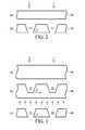
- FIG. 1is a flowchart illustrating a method of fabricating a semiconductor device according to various aspects of the present disclosure.
- FIG. 2illustrates laser etching an opening through a substrate of a semiconductor device according to aspects of the present disclosure.
- FIG. 3illustrates laser etching an opening through a portion of a substrate and then exposing the opening according to aspects of the present disclosure.
- FIGS. 4A-4Iillustrate sectional views of stages in forming a semiconductor device according to various aspects of the present disclosure.
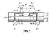
- FIG. 5illustrates another embodiment of a semiconductor device according to various aspects of the present disclosure.
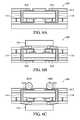
- FIGS. 6A-6Cillustrate sectional views of stages in forming another semiconductor device according to various aspects of the present disclosure.
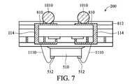
- FIG. 7illustrates yet another embodiment of a semiconductor device according to various aspects of the present disclosure.
- the present disclosureprovides for many different embodiments.
- One of the broader forms of the present disclosureinvolves a method of fabricating a semiconductor device.
- the methodincludes providing a substrate having a frontside and a backside, and providing a layer above the frontside of the substrate, the layer having a different composition from the substrate.
- the methodfurther includes controlling a laser power and a laser pulse number to laser etch an opening through the layer and at least a portion of the frontside of the substrate, filling the opening with a conductive material to form a via, removing a portion of the backside of the substrate to expose the via, and electrically coupling a first element to a second element with the via.
- Another of the broader forms of the present disclosureinvolves another method of fabricating a semiconductor device, the method including providing a substrate having a frontside and a backside, and providing a plurality of layers above the frontside of the substrate, the layers having different compositions from the substrate.
- the methodfurther includes controlling a laser power and a laser pulse number to laser etch an opening through the plurality of layers and at least a portion of the frontside of the substrate, wherein a taper angle of the opening is tuned by the laser power and the laser pulse number.
- the methodcontinues with filling the opening with a conductive material to form a via, removing a portion of the backside of the substrate to expose the via, and electrically coupling a first element to a second element with the via.
- the semiconductor deviceincludes a first die having a first surface and a second surface opposite the first surface, and a plurality of vias formed through a plurality of openings laser-etched through the first surface of the first die, each opening of the plurality of openings having an aspect ratio ranging between about 0.25 and about 20.
- the devicefurther includes a first set of redistribution lines electrically coupling semiconductor components of the first die to the plurality of vias, and a second die having a first surface and a second surface opposite the first surface.
- the first surface of the second diehas contact pads, the first set of redistribution lines electrically coupling the contact pads of the second die to the plurality of vias.
- the present disclosurerelates generally to the fabrication of a semiconductor device, and more particularly, to methods for providing vias in a semiconductor substrate and devices fabricated by such methods.
- first and second featuresare formed in direct contact
- additional featuresmay be formed between the first and second features, such that the first and second features may not be in direct contact
- present disclosuremay repeat reference numerals and/or letters in the various examples. This repetition is for the purpose of simplicity and clarity and does not in itself dictate a relationship between the various embodiments and/or configurations discussed.
- FIG. 1Illustrated in FIG. 1 is a flowchart of an example method for fabricating a semiconductor device.
- FIGS. 2 and 3illustrate different methods of controlling a laser power and a laser pulse number to laser etch an opening through at least a portion of a substrate in accordance with various aspects of the present disclosure.
- Illustrated in FIGS. 4A-4Iare cross-sectional views of stages in forming a semiconductor device according to various aspects of the present disclosure.
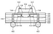
- FIG. 5illustrates another embodiment of a semiconductor device according to various aspects of the present disclosure
- FIGS. 6A-6Cillustrate sectional views of stages in forming another semiconductor device according to various aspects of the present disclosure
- FIG. 7illustrates yet another embodiment of a semiconductor device according to various aspects of the present disclosure.
- like reference numbersare used to designate like elements.
- a method 10for forming a semiconductor device.
- the method 10includes providing a substrate at block 12 , and controlling a laser power and a laser pulse number to laser etch an opening through at least a portion of the substrate at block 14 .
- the methodfurther includes forming a liner layer in the laser-etched opening at block 16 .
- the methodcontinues with filling the opening with a conductive material to form a via at block 18 , and electrically coupling a first element to a second element with the via at block 20 .
- the semiconductor devicemay include an integrated circuit (IC) chip (both 2D and 3D IC designs), a system on chip (SoC), or portion thereof, that may include various passive and active microelectronic devices, such as resistors, capacitors, inductors, diodes, metal-oxide-semiconductor field effect transistors (MOSFET), complementary MOS (CMOS) transistors, bipolar junction transistors (BJT), laterally diffused MOS (LDMOS) transistors, high power MOS transistors, FinFET transistors, or other types of transistors.
- MOSFETmetal-oxide-semiconductor field effect transistors
- CMOScomplementary MOS
- BJTbipolar junction transistors
- LDMOSlaterally diffused MOS
- the substrates 30 and 40each include silicon.
- the substratesmay alternatively or additionally include other elementary semiconductor material such as germanium, diamond, ceramic, and/or sapphire.
- the substratesmay also include a compound semiconductor material such as silicon carbide, gallium arsenide, gallium nitride, indium arsenide, and/or indium phosphide.
- the substratesmay include an alloy semiconductor such as silicon germanium, silicon germanium carbide, gallium arsenic phosphide, and/or gallium indium phosphide.
- the substratesmay also include various p-type doped regions and/or n-type doped regions. All doping may be implemented using a process such as ion implantation or diffusion in various steps and techniques.
- the substratesmay include conventional isolation features, known in the art, to separate different devices formed in the substrate.
- the substratemay include other features such as an epitaxial layer, a semiconductor on insulator (SOI) structure, or combinations thereof.
- SOIsemiconductor on insulator
- Block arrows in FIGS. 2( a ) and 3 ( a )illustrate pulsating laser light at a controlled laser power and a laser pulse number to etch through the substrate 30 and a portion of substrate 40 , respectively.
- the laser power and the laser pulse numberare controlled parameters for the via formation, and may be inversely related, as decreased pulse number is needed with increased laser power to create a similar opening, and increased pulse number is needed with decreased laser power to create a similar opening.
- the pulse numbermay be controlled by manipulating a wafer stage or a laser shutter.
- the laseris operated in a pulse mode to bombard an etch surface at a pulsing frequency, thereby allowing for improved etching rates and smooth sidewall formation.
- the laser lightmay be provided by various lasers, including but not limited to KrF, XeF, XeCl, CO 2 , Nd:YAG, and He:Cd lasers.
- the laser lightmay also be provided at various wavelengths, including but not limited to KrF at 248 nm, XeF at 351 nm, XeCl at 308 nm, CO 2 at 10600 nm, Nd:YAG at 1064 nm, 532 nm, or 355 nm, and He:Cd at 325 nm.
- the laser lightmay be provided within a range of power, from about 1 milliwatt to about 100 kilowatts in one example.
- a laser power for a CO 2 lasermay range from several milliwatt to hundreds of kilowatts
- a laser power for a Nd:YAG lasermay range from one milliwatt to 45 watts
- a laser power for a KrF lasermay be less than 100 watts.
- the laser lightmay be provided within a range of pulse number, from about 1 to 300 in one example.
- laser-etched openingsmay have a diameter ranging between about 40 micron and about 140 micron, and a depth ranging between about 10 micron and about 800 micron, with an aspect ratio ranging between about 0.25 and about 20.
- laser-etched openingsmay have a diameter ranging between about 40 micron and about 140 micron, and a depth ranging between about 200 micron and about 400 micron, with an aspect ratio ranging between about 5 and about 10.
- Laser-etched openings 31 and 41 having tapered angles ⁇are illustrated in FIGS. 2( b ) and 3 ( b ), respectively. Tapered angles ⁇ are measured from the horizontal plane and may range between about 60 degrees and about 90 degrees (i.e., vertical sidewalls).
- the tapered angle of laser-etched openings 31 and 41may be tuned by the type of laser, wavelength of laser light, laser power, and/or laser pulse number used, in one example. In certain applications, such as oxide deposition or electroplating, v-shaped openings having tapered angles less than 90 degrees may allow for improved oxide coverage and/or electroplating quality.
- laser etching of high aspect ratio openings for high aspect ratio via formationallows for increased etch rates, increased uniformity of sidewall profiles, single step etching through various layers of materials with a single laser type, and no requirement of pre-process lithography patterning.
- the etch ratemay be less than 10 milliseconds to etch through a 400 micron thick silicon wafer.
- FIG. 3( c )illustrates blind via formation by grinding and polishing of remaining substrate 40 to expose opening 41 .
- Blind via formationmay be advantageous for thermal dissipation and female die applications. It is also noted that multiple layers of materials may be laser-etched in one process step as will be illustrated with respect to FIGS. 4A-4I below.
- the semiconductor substrate 110may comprise, for example, bulk silicon, doped or undoped, or an active layer of a semiconductor-on-insulator (SOI) substrate.
- SOIsemiconductor-on-insulator
- an SOIcomprises a layer of a semiconductor material, such as silicon, formed on an insulator layer.
- the insulator layermay be, for example, a buried oxide (BOX) layer or a silicon oxide layer.
- BOXburied oxide
- the insulator layeris provided on a substrate, typically a silicon or glass substrate. Other substrates, such as a multi-layered or gradient substrate may also be used.
- the electrical circuitry 112 formed on the semiconductor substrate 110may be any type of circuitry suitable for a particular application.
- the circuitryincludes electrical devices formed on the substrate with one or more dielectric layers 120 overlying the electrical devices.
- Layer 120is illustrated as a single layer for illustrative purposes only and may comprise a plurality of layers of different materials.
- Metal layersmay be formed between dielectric layers to route electrical signals between the electrical devices.
- Electrical devicesmay also be formed in one or more dielectric layers.
- the electrical circuitry 112may include various N-type metal-oxide semiconductor (NMOS) and/or P-type metal-oxide semiconductor (PMOS) devices, such as transistors, capacitors, resistors, diodes, photo-diodes, fuses, and the like, interconnected to perform one or more functions.
- the functionsmay include memory structures, processing structures, sensors, amplifiers, power distribution, input/output circuitry, or the like.
- FIG. 4Billustrates laser-etched openings 101 through dielectric layer 120 and a portion of substrate 110 .
- Openings 101may be advantageously formed in a single process step with increased etch speed and uniformity of opening sidewalls by tuning various lasers at various controlled laser power, laser pulse number, and/or laser frequency as noted above.
- FIG. 4Cillustrates through-silicon vias 114 formed by providing conductive material within laser-etched openings 101 .
- the through-silicon vias 114may be formed by any appropriate method. For example, in one embodiment the through-silicon vias 114 are formed after the electrical circuitry 112 is formed. In this embodiment, openings 101 are formed through dielectric layer 120 and partially through the semiconductor substrate 110 . The openings 101 may be optionally lined with a liner layer 114 a , such as diffusion barrier layers, adhesion layers, isolation layer, or the like, and then filled with a conductive material to form vias 114 .
- a liner layer 114 asuch as diffusion barrier layers, adhesion layers, isolation layer, or the like
- Diffusion barrier layersmay comprise one or more layers of TaN, Ta, TiN, Ti, CoW, or the like, and the conductive material comprises copper, tungsten, aluminum, silver, and combinations thereof, or the like, thereby forming the through-silicon vias 114 .
- the through-silicon vias 114have a diffusion barrier layer of TaN and are filled with copper formed by an electro-chemical plating process in which a seed layer is deposited to aid in the formation of the conductive fill material.
- FIG. 4Dillustrates the formation of redistribution lines 116 .
- the redistribution lines 116electrically couple the electrical circuitry 112 (via contact plugs 118 ) to the through-silicon vias 114 .
- the redistribution lines 116may be formed using common methods for forming interconnect lines in integrated circuits.
- the redistribution lines 116are fabricated by forming a layer of copper and a layer of nickel over the layer of copper through sputter, chemical vapor deposition, electrical plating, pattern electrical plating, or electroless plating, and then etching the undesired portions to form the redistribution lines 116 .
- Other materialssuch as aluminum, tungsten, titanium, combinations thereof, or the like may be used.
- the redistribution lines 116have a thickness between about 0.5 micron and about 30 micron. Other materials and processes, such as a well-known damascene process, could alternatively be used to form the redistribution lines 116 .
- the redistribution lines 116are covered with a passivation layer 122 .
- the passivation layer 122comprises a high-heat resistant material in one example. It should be noted that the passivation layer 122 is illustrated as a single layer for illustrative purposes only and may comprise a plurality of layers of different materials. Suitable materials that may be used to form the passivation layer 122 include polyimide, BCB, SOG, SiOx, SiNx, SiONx, other inorganic materials, other silicon-related materials, other high thermal stable polymers, and the like.
- FIG. 4Eillustrates the portion of the wafer 100 after a carrier wafer 210 has been attached in accordance with an embodiment of the present disclosure.
- the carrier wafer 210provides temporary mechanical and structural support to the wafer 100 during subsequent processing steps. In this manner, damage to the semiconductor substrate 110 is reduced or prevented.
- the carrier wafer 210may comprise, for example, glass, silicon oxide, aluminum oxide, and the like.
- an adhesive(not shown) is used to glue the carrier wafer 210 to a top surface of the passivation layer 122 .
- the adhesivemay be any suitable adhesive, such as an ultraviolet (UV) glue, which loses its adhesive property when exposed to UV lights.
- UVultraviolet
- the thickness of the carrier wafer 210is greater than about 12 millimeters in one example.
- the through-silicon vias 114are exposed using a combination of planarizing and etching steps. Initially, a planarizing process, such as grinding or a chemical mechanical polishing (CMP), may be performed to initially expose the through-silicon vias 114 . Thereafter, an etching process may be performed to recess the semiconductor substrate 110 , thereby leaving the through-silicon vias 114 protruding from the underside of the semiconductor substrate 110 as illustrated in FIG. 4E .
- a planarizing processsuch as grinding or a chemical mechanical polishing (CMP)
- CMPchemical mechanical polishing
- the semiconductor substrate 110may be recessed by performing a dry etch process using HBr/O 2 , HBr/Cl 2 /O 2 , SF 6 /CL 2 , SF 6 plasma, or the like. In one example, about 5 micron to about 30 micron of the through-silicon vias 114 are exposed.
- FIG. 4Fillustrates the wafer 100 after a protective coating 310 has been applied in accordance with an embodiment of the present disclosure.
- the protective coating 310is an epoxy, gel, silicon rubber, or the like, and may be dispensed by, for example, spin-coating or printing.
- the protective coating 310is formed having a thickness sufficient to cover the exposed through-silicon vias 114 .
- a second planarizing processsuch as grinding or CMP, is performed such that a substantially planar surface is formed and the through-silicon vias 114 are exposed as illustrated in FIG. 4F .
- FIG. 4Gillustrates the wafer 100 after the carrier wafer 210 is removed in accordance with an embodiment of the present disclosure.
- a UV glueis used to attach the carrier wafer 210 to the wafer 100 as discussed above, the UV glue is exposed to UV light, thereby causing the UV glue, for example, to become non-adhesive. Thereafter, the carrier wafer 210 may be easily detached.
- Other types of adhesivemay be used, which may be released using, for example, thermal, solvent/plasma stripper, laser, or the like techniques.
- FIG. 4Hillustrates the wafer 100 after a second die 510 has been attached in accordance with an embodiment of the present disclosure.
- the second die 510is illustrated as being smaller than the first die for illustrative purposes only, and that the sizes of the first die and the second die 510 may vary such that the first die may be smaller or larger or the same size as the second die 510 .
- the second die 510is electrically coupled to the first die in a flip-chip configuration such that contact pads 512 face the first die.
- the contact pads 512are electrically coupled to the redistribution lines 116 via solder balls 514 , which may be formed by a high-lead, eutectic, lead free solder, Cu bump, Cu/Sn, or the like.
- An optional underfill material 516may be injected or otherwise formed in the space between the second die 510 and the passivation layer 122 .
- the underfill material 516may, for example, comprise a liquid epoxy that is dispensed between the second die 510 and the passivation layer 122 , and then cured to harden. This underfill material 516 is used, among other things, to prevent cracks from being formed in the solder balls 514 , wherein cracks are typically caused by thermal stresses.
- either a deformable gel or silicon rubbercould be formed between the second die 510 and the passivation layer 122 in order to help prevent cracks from occurring within the solder balls 514 .
- This gel or silicon rubbermay be formed by injecting or otherwise placing the gel or rubber between the second die 510 and the passivation layer 122 .
- the deformable gel or silicon rubbercan provide greater stress relief.
- wire bondingmay be used to electrically couple contact pads of the second die laying face up to the redistribution lines 116 , as discussed below with reference to FIG. 5 .
- solder mask 610 and second solder balls 612may be formed in accordance with an embodiment of the present disclosure as illustrated in FIG. 4I .
- the solder mask 610may be formed by depositing and patterning a solder mask material to expose contact regions of the underlying redistribution lines 116 .
- the second solder balls 612comprising a high-lead, eutectic, or lead free solder, or the like may be formed.
- the processes of forming and patterning a solder mask and forming solder ballsare well-known in the art and, thus, are not repeated herein.
- the second solder balls 612may be formed by other methods.
- an under-bump metallization (UBM)may be deposited over the protective coating 310 and second solder balls 612 formed thereon by, for example, evaporation, electroplating, printing, jetting, stud bumping, direct placement, or the like.
- the second solder balls 612may be formed directly on the through-silicon vias 114 .
- the redistribution lines 116may comprise lines electrically coupling semiconductor structures formed on the first semiconductor die 110 , such as electrical circuitry 112 , to the through-silicon vias 114 (and to the second solder balls 612 ) or lines electrically coupling semiconductor structures (not shown) formed on the second semiconductor die 510 to the through-silicon vias 114 (and to the second solder balls 612 ). Additionally, semiconductor structures on both the first semiconductor die and the second semiconductor die 510 may be electrically coupled to the same redistribution line.
- an encapsulantmay be formed, a singulation process may be performed to singulate individual stacked-die packages, and the like.
- FIG. 5illustrates an embodiment in which the second die 510 is electrically coupled to the redistribution lines 116 using wire bonds 710 as is known in the art.
- the second die 510is attached to the first die such that the contact pads 512 on the second die 510 face away from the first die.
- Wire bonds 710extend over the side of the first die and electrically couple the contact pads 512 to respective ones of the first set of redistribution lines 116 .
- FIGS. 6A-6Ca second embodiment is illustrated in which double-sided redistribution lines are used to allow for greater flexibility in a pin-out configuration in accordance with an embodiment of the present disclosure.
- FIG. 6Aassumes a wafer 200 that has been formed in a manner similar to that discussed above with reference to FIGS. 4A-4F , wherein like reference numerals refer to like elements.
- FIG. 6Aillustrates wafer 200 , which corresponds to wafer 100 of FIG. 4F after backside redistribution lines 810 and a solder mask 812 have been formed, in accordance with an embodiment of the present disclosure.
- the backside redistribution lines 810may be formed in a similar manner and of similar materials as the redistribution lines 116 discussed above with reference to FIG. 4D .
- the solder mask 812may be formed in a similar manner as solder mask 610 discussed above with reference to FIG. 4I .
- FIG. 6Billustrates the second die 510 attached to the wafer 200 in accordance with an embodiment of the present disclosure.
- the second die 510may be attached to the wafer 800 using solder balls 514 and underfill material 516 as described above with reference to FIG. 4H .
- FIG. 6Cillustrates formation of solder balls 1010 in accordance with an embodiment of the present disclosure.
- FIG. 7illustrates an embodiment in which the second die 510 of FIGS. 6A-6C is electrically coupled to the first die 130 using wire bonds 1110 as are known in the art.
- the second die 510is attached to the first die 130 such that the contact pads 512 on the second die 510 face away from the first die 130 .
- Wire bonds 1110extend over the side of the first die and electrically couple the contact pads 512 to respective ones of the first set of redistribution lines 116 .
- the present disclosureprovides a method to fabricate a semiconductor device.
- the methodincludes providing a substrate having a frontside and a backside, and providing a layer above the frontside of the substrate, the layer having a different composition from the substrate.
- the methodfurther includes controlling a laser power and a laser pulse number to laser etch an opening through the layer and at least a portion of the frontside of the substrate, filling the opening with a conductive material to form a via, removing a portion of the backside of the substrate to expose the via, and electrically coupling a first element to a second element with the via.
- the present disclosureprovides another method to fabricate a semiconductor device.
- the methodincludes providing a substrate having a frontside and a backside, and providing a plurality of layers above the frontside of the substrate, the layers having different compositions from the substrate.
- the methodfurther includes controlling a laser power and a laser pulse number to laser etch an opening through the plurality of layers and at least a portion of the frontside of the substrate, wherein a taper angle of the opening is tuned by the laser power and the laser pulse number.
- the methodcontinues with filling the opening with a conductive material to form a via, removing a portion of the backside of the substrate to expose the via, and electrically coupling a first element to a second element with the via.
- the semiconductor deviceincludes a first die having a first surface and a second surface opposite the first surface, and a plurality of vias formed through a plurality of openings laser-etched through the first surface of the first die, each opening of the plurality of openings having an aspect ratio ranging between about 0.25 and about 20.
- the devicefurther includes a first set of redistribution lines electrically coupling semiconductor components of the first die to the plurality of vias, and a second die having a first surface and a second surface opposite the first surface.
- the first surface of the second diehas contact pads, the first set of redistribution lines electrically coupling the contact pads of the second die to the plurality of vias.
- additional processesmay be performed to complete the fabrication of the semiconductor device.
- these additional processesmay include deposition of passivation layers, formation of contacts, and formation of interconnect structures (e.g., lines and vias, metal layers, and interlayer dielectric that provide electrical interconnection to the device including the formed metal gate).
- interconnect structurese.g., lines and vias, metal layers, and interlayer dielectric that provide electrical interconnection to the device including the formed metal gate.
- these additional processesmay not be necessarily described herein.
Landscapes
- Engineering & Computer Science (AREA)
- Microelectronics & Electronic Packaging (AREA)
- Power Engineering (AREA)
- Computer Hardware Design (AREA)
- Physics & Mathematics (AREA)
- Condensed Matter Physics & Semiconductors (AREA)
- General Physics & Mathematics (AREA)
- Manufacturing & Machinery (AREA)
- Internal Circuitry In Semiconductor Integrated Circuit Devices (AREA)
Abstract
Description
Claims (21)
Priority Applications (2)
| Application Number | Priority Date | Filing Date | Title |
|---|---|---|---|
| US12/768,911US8519538B2 (en) | 2010-04-28 | 2010-04-28 | Laser etch via formation |
| CN201010569544.1ACN102237301B (en) | 2010-04-28 | 2010-11-30 | Semiconductor device and manufacturing method thereof |
Applications Claiming Priority (1)
| Application Number | Priority Date | Filing Date | Title |
|---|---|---|---|
| US12/768,911US8519538B2 (en) | 2010-04-28 | 2010-04-28 | Laser etch via formation |
Publications (2)
| Publication Number | Publication Date |
|---|---|
| US20110266674A1 US20110266674A1 (en) | 2011-11-03 |
| US8519538B2true US8519538B2 (en) | 2013-08-27 |
Family
ID=44857599
Family Applications (1)
| Application Number | Title | Priority Date | Filing Date |
|---|---|---|---|
| US12/768,911Expired - Fee RelatedUS8519538B2 (en) | 2010-04-28 | 2010-04-28 | Laser etch via formation |
Country Status (2)
| Country | Link |
|---|---|
| US (1) | US8519538B2 (en) |
| CN (1) | CN102237301B (en) |
Cited By (3)
| Publication number | Priority date | Publication date | Assignee | Title |
|---|---|---|---|---|
| US10008418B2 (en) | 2016-09-30 | 2018-06-26 | Taiwan Semiconductor Manufacturing Co., Ltd. | Method of semiconductor integrated circuit fabrication |
| US10115624B2 (en) | 2016-06-30 | 2018-10-30 | Taiwan Semiconductor Manufacturing Co., Ltd. | Method of semiconductor integrated circuit fabrication |
| US20220028699A1 (en)* | 2020-07-21 | 2022-01-27 | Infineon Technologies Austria Ag | Chip-substrate composite semiconductor device |
Families Citing this family (23)
| Publication number | Priority date | Publication date | Assignee | Title |
|---|---|---|---|---|
| US8569876B2 (en) | 2006-11-22 | 2013-10-29 | Tessera, Inc. | Packaged semiconductor chips with array |
| US8405196B2 (en) | 2007-03-05 | 2013-03-26 | DigitalOptics Corporation Europe Limited | Chips having rear contacts connected by through vias to front contacts |
| US8796135B2 (en) | 2010-07-23 | 2014-08-05 | Tessera, Inc. | Microelectronic elements with rear contacts connected with via first or via middle structures |
| US8791575B2 (en) | 2010-07-23 | 2014-07-29 | Tessera, Inc. | Microelectronic elements having metallic pads overlying vias |
| US9640437B2 (en) | 2010-07-23 | 2017-05-02 | Tessera, Inc. | Methods of forming semiconductor elements using micro-abrasive particle stream |
| US8847380B2 (en) | 2010-09-17 | 2014-09-30 | Tessera, Inc. | Staged via formation from both sides of chip |
| US8610259B2 (en) | 2010-09-17 | 2013-12-17 | Tessera, Inc. | Multi-function and shielded 3D interconnects |
| US8587126B2 (en) | 2010-12-02 | 2013-11-19 | Tessera, Inc. | Stacked microelectronic assembly with TSVs formed in stages with plural active chips |
| US8736066B2 (en) | 2010-12-02 | 2014-05-27 | Tessera, Inc. | Stacked microelectronic assemby with TSVS formed in stages and carrier above chip |
| US8637968B2 (en) | 2010-12-02 | 2014-01-28 | Tessera, Inc. | Stacked microelectronic assembly having interposer connecting active chips |
| US8610264B2 (en) | 2010-12-08 | 2013-12-17 | Tessera, Inc. | Compliant interconnects in wafers |
| ITTO20120294A1 (en) | 2012-04-03 | 2013-10-04 | St Microelectronics Srl | PERFECTED ELECTRIC TESTING SYSTEM FOR THROUGH WAYS IN THE SILICON (TSV-THROUGH SILICON VIAS) AND ITS PROCESS OF PROCESSING |
| US9728458B2 (en)* | 2012-07-31 | 2017-08-08 | Soitec | Methods for fabrication of semiconductor structures using laser lift-off process, and related semiconductor structures |
| US9059044B2 (en) | 2012-11-15 | 2015-06-16 | International Business Machines Corporation | On-chip diode with fully depleted semiconductor devices |
| US20140151700A1 (en)* | 2012-12-04 | 2014-06-05 | Thorsten Meyer | Chip package and a method for manufacturing a chip package |
| US20140199833A1 (en)* | 2013-01-11 | 2014-07-17 | Applied Materials, Inc. | Methods for performing a via reveal etching process for forming through-silicon vias in a substrate |
| US9082698B1 (en)* | 2014-03-07 | 2015-07-14 | Globalfoundries Inc. | Methods to improve FinFet semiconductor device behavior using co-implantation under the channel region |
| CN108346639B (en)* | 2017-09-30 | 2020-04-03 | 中芯集成电路(宁波)有限公司 | Wafer level system packaging method and packaging structure |
| US20200083132A1 (en)* | 2018-09-07 | 2020-03-12 | Advanced Semiconductor Engineering, Inc. | Semiconductor device package |
| US11437322B2 (en) | 2018-09-07 | 2022-09-06 | Advanced Semiconductor Engineering, Inc. | Semiconductor device package |
| CN111162054B (en)* | 2019-12-31 | 2022-01-11 | 中芯集成电路(宁波)有限公司 | Wafer-level chip packaging method and packaging structure |
| US20230378039A1 (en)* | 2022-05-23 | 2023-11-23 | Taiwan Semiconductor Manufacturing Company, Ltd. | Semiconductor package and methods of manufacturing |
| US20240047297A1 (en)* | 2022-08-08 | 2024-02-08 | nD-HI Technologies Lab, Inc. | Manufacturing method of diamond composite wafer |
Citations (41)
| Publication number | Priority date | Publication date | Assignee | Title |
|---|---|---|---|---|
| US5391917A (en) | 1993-05-10 | 1995-02-21 | International Business Machines Corporation | Multiprocessor module packaging |
| US5510298A (en) | 1991-09-12 | 1996-04-23 | Texas Instruments Incorporated | Method of interconnect in an integrated circuit |
| US5527739A (en)* | 1993-12-23 | 1996-06-18 | Motorola, Inc. | Process for fabricating a semiconductor device having an improved metal interconnect structure |
| US5767001A (en) | 1993-05-05 | 1998-06-16 | Siemens Aktiengesellschaft | Process for producing semiconductor components between which contact is made vertically |
| US5998292A (en) | 1997-11-12 | 1999-12-07 | International Business Machines Corporation | Method for making three dimensional circuit integration |
| US6184060B1 (en) | 1996-10-29 | 2001-02-06 | Trusi Technologies Llc | Integrated circuits and methods for their fabrication |
| US6322903B1 (en) | 1999-12-06 | 2001-11-27 | Tru-Si Technologies, Inc. | Package of integrated circuits and vertical integration |
| US20010053567A1 (en)* | 1999-02-16 | 2001-12-20 | Salman Akram | Method of forming a test insert for interfacing a device containing contact bumps with a test substrate |
| US6448168B1 (en) | 1997-09-30 | 2002-09-10 | Intel Corporation | Method for distributing a clock on the silicon backside of an integrated circuit |
| US6465892B1 (en) | 1999-04-13 | 2002-10-15 | Oki Electric Industry Co., Ltd. | Interconnect structure for stacked semiconductor device |
| US20020151171A1 (en)* | 2001-03-28 | 2002-10-17 | Seiko Epson Corporation | Semiconductor device and manufacturing method therefor, circuit substrate, and electronic apparatus |
| US6538333B2 (en) | 2000-06-16 | 2003-03-25 | Chartered Semiconductor Manufacturing Ltd. | Three dimensional IC package module |
| US6599778B2 (en) | 2001-12-19 | 2003-07-29 | International Business Machines Corporation | Chip and wafer integration process using vertical connections |
| US6664129B2 (en) | 1996-10-29 | 2003-12-16 | Tri-Si Technologies, Inc. | Integrated circuits and methods for their fabrication |
| US6790775B2 (en)* | 2002-10-31 | 2004-09-14 | Hewlett-Packard Development Company, L.P. | Method of forming a through-substrate interconnect |
| US6800930B2 (en) | 2002-07-31 | 2004-10-05 | Micron Technology, Inc. | Semiconductor dice having back side redistribution layer accessed using through-silicon vias, and assemblies |
| US6841883B1 (en) | 2003-03-31 | 2005-01-11 | Micron Technology, Inc. | Multi-dice chip scale semiconductor components and wafer level methods of fabrication |
| US6908784B1 (en)* | 2002-03-06 | 2005-06-21 | Micron Technology, Inc. | Method for fabricating encapsulated semiconductor components |
| US6924551B2 (en) | 2003-05-28 | 2005-08-02 | Intel Corporation | Through silicon via, folded flex microelectronic package |
| US6962872B2 (en) | 2002-12-09 | 2005-11-08 | International Business Machines Corporation | High density chip carrier with integrated passive devices |
| US20060027934A1 (en)* | 2003-12-05 | 2006-02-09 | International Business Machines Corporation | Silicon chip carrier with conductive through-vias and method for fabricating same |
| US7049170B2 (en) | 2003-12-17 | 2006-05-23 | Tru-Si Technologies, Inc. | Integrated circuits and packaging substrates with cavities, and attachment methods including insertion of protruding contact pads into cavities |
| US7060601B2 (en) | 2003-12-17 | 2006-06-13 | Tru-Si Technologies, Inc. | Packaging substrates for integrated circuits and soldering methods |
| US7071546B2 (en) | 2002-01-16 | 2006-07-04 | Alfred E. Mann Foundation For Scientific Research | Space-saving packaging of electronic circuits |
| US7111149B2 (en) | 2003-07-07 | 2006-09-19 | Intel Corporation | Method and apparatus for generating a device ID for stacked devices |
| US7122912B2 (en) | 2004-01-28 | 2006-10-17 | Nec Electronics Corporation | Chip and multi-chip semiconductor device using thereof and method for manufacturing same |
| US7157787B2 (en) | 2002-02-20 | 2007-01-02 | Intel Corporation | Process of vertically stacking multiple wafers supporting different active integrated circuit (IC) devices |
| US7193308B2 (en) | 2003-09-26 | 2007-03-20 | Seiko Epson Corporation | Intermediate chip module, semiconductor device, circuit board, and electronic device |
| US7262495B2 (en) | 2004-10-07 | 2007-08-28 | Hewlett-Packard Development Company, L.P. | 3D interconnect with protruding contacts |
| US20070262464A1 (en)* | 2004-08-24 | 2007-11-15 | Micron Technology, Inc. | Method of forming vias in semiconductor substrates and resulting structures |
| US7297574B2 (en) | 2005-06-17 | 2007-11-20 | Infineon Technologies Ag | Multi-chip device and method for producing a multi-chip device |
| US7335972B2 (en) | 2003-11-13 | 2008-02-26 | Sandia Corporation | Heterogeneously integrated microsystem-on-a-chip |
| US20080111213A1 (en)* | 2004-09-02 | 2008-05-15 | Micron Technology, Inc. | Through-wafer interconnects for photoimager and memory wafers |
| US20080284037A1 (en)* | 2007-05-15 | 2008-11-20 | Andry Paul S | Apparatus and Methods for Constructing Semiconductor Chip Packages with Silicon Space Transformer Carriers |
| US20080290525A1 (en)* | 2007-05-21 | 2008-11-27 | International Business Machines Corporation | Silicon-on-insulator structures for through via in silicon carriers |
| US7514797B2 (en) | 2007-05-31 | 2009-04-07 | Taiwan Semiconductor Manufacturing Company, Ltd. | Multi-die wafer level packaging |
| US7575999B2 (en)* | 2004-09-01 | 2009-08-18 | Micron Technology, Inc. | Method for creating conductive elements for semiconductor device structures using laser ablation processes and methods of fabricating semiconductor device assemblies |
| US20090243074A1 (en) | 2008-03-31 | 2009-10-01 | Chandrasekaram Ramiah | Semiconductor through silicon vias of variable size and method of formation |
| US20100015782A1 (en)* | 2008-07-18 | 2010-01-21 | Chen-Hua Yu | Wafer Dicing Methods |
| US8018045B2 (en)* | 1998-09-28 | 2011-09-13 | Ibiden Co., Ltd. | Printed circuit board |
| US8324101B2 (en)* | 2005-09-01 | 2012-12-04 | Micron Technology, Inc. | Semiconductor dice including at least one blind hole, wafers including such semiconductor dice, and intermediate products made while forming at least one blind hole in a substrate |
Family Cites Families (3)
| Publication number | Priority date | Publication date | Assignee | Title |
|---|---|---|---|---|
| US7101792B2 (en)* | 2003-10-09 | 2006-09-05 | Micron Technology, Inc. | Methods of plating via interconnects |
| US7560371B2 (en)* | 2006-08-29 | 2009-07-14 | Micron Technology, Inc. | Methods for selectively filling apertures in a substrate to form conductive vias with a liquid using a vacuum |
| CN100570846C (en)* | 2007-12-06 | 2009-12-16 | 清华大学 | High Aspect Ratio 3D Vertical Interconnection and Implementation Method of 3D Integrated Circuit |
- 2010
- 2010-04-28USUS12/768,911patent/US8519538B2/ennot_activeExpired - Fee Related
- 2010-11-30CNCN201010569544.1Apatent/CN102237301B/enactiveActive
Patent Citations (53)
| Publication number | Priority date | Publication date | Assignee | Title |
|---|---|---|---|---|
| US5510298A (en) | 1991-09-12 | 1996-04-23 | Texas Instruments Incorporated | Method of interconnect in an integrated circuit |
| US5767001A (en) | 1993-05-05 | 1998-06-16 | Siemens Aktiengesellschaft | Process for producing semiconductor components between which contact is made vertically |
| US5391917A (en) | 1993-05-10 | 1995-02-21 | International Business Machines Corporation | Multiprocessor module packaging |
| US5527739A (en)* | 1993-12-23 | 1996-06-18 | Motorola, Inc. | Process for fabricating a semiconductor device having an improved metal interconnect structure |
| US6882030B2 (en) | 1996-10-29 | 2005-04-19 | Tru-Si Technologies, Inc. | Integrated circuit structures with a conductor formed in a through hole in a semiconductor substrate and protruding from a surface of the substrate |
| US6639303B2 (en) | 1996-10-29 | 2003-10-28 | Tru-Si Technolgies, Inc. | Integrated circuits and methods for their fabrication |
| US6740582B2 (en) | 1996-10-29 | 2004-05-25 | Tru-Si Technologies, Inc. | Integrated circuits and methods for their fabrication |
| US6184060B1 (en) | 1996-10-29 | 2001-02-06 | Trusi Technologies Llc | Integrated circuits and methods for their fabrication |
| US6664129B2 (en) | 1996-10-29 | 2003-12-16 | Tri-Si Technologies, Inc. | Integrated circuits and methods for their fabrication |
| US6448168B1 (en) | 1997-09-30 | 2002-09-10 | Intel Corporation | Method for distributing a clock on the silicon backside of an integrated circuit |
| US5998292A (en) | 1997-11-12 | 1999-12-07 | International Business Machines Corporation | Method for making three dimensional circuit integration |
| US8018045B2 (en)* | 1998-09-28 | 2011-09-13 | Ibiden Co., Ltd. | Printed circuit board |
| US20010053567A1 (en)* | 1999-02-16 | 2001-12-20 | Salman Akram | Method of forming a test insert for interfacing a device containing contact bumps with a test substrate |
| US6472293B2 (en) | 1999-04-13 | 2002-10-29 | Oki Electric Industry Co., Ltd. | Method for manufacturing an interconnect structure for stacked semiconductor device |
| US6465892B1 (en) | 1999-04-13 | 2002-10-15 | Oki Electric Industry Co., Ltd. | Interconnect structure for stacked semiconductor device |
| US6693361B1 (en) | 1999-12-06 | 2004-02-17 | Tru-Si Technologies, Inc. | Packaging of integrated circuits and vertical integration |
| US6322903B1 (en) | 1999-12-06 | 2001-11-27 | Tru-Si Technologies, Inc. | Package of integrated circuits and vertical integration |
| US6538333B2 (en) | 2000-06-16 | 2003-03-25 | Chartered Semiconductor Manufacturing Ltd. | Three dimensional IC package module |
| US20020151171A1 (en)* | 2001-03-28 | 2002-10-17 | Seiko Epson Corporation | Semiconductor device and manufacturing method therefor, circuit substrate, and electronic apparatus |
| US6599778B2 (en) | 2001-12-19 | 2003-07-29 | International Business Machines Corporation | Chip and wafer integration process using vertical connections |
| US7071546B2 (en) | 2002-01-16 | 2006-07-04 | Alfred E. Mann Foundation For Scientific Research | Space-saving packaging of electronic circuits |
| US7157787B2 (en) | 2002-02-20 | 2007-01-02 | Intel Corporation | Process of vertically stacking multiple wafers supporting different active integrated circuit (IC) devices |
| US6908784B1 (en)* | 2002-03-06 | 2005-06-21 | Micron Technology, Inc. | Method for fabricating encapsulated semiconductor components |
| US7417325B2 (en)* | 2002-03-06 | 2008-08-26 | Micron Technology, Inc. | Semiconductor component having thinned die with conductive vias configured as conductive pin terminal contacts |
| US20060275949A1 (en)* | 2002-03-06 | 2006-12-07 | Farnworth Warren M | Semiconductor components and methods of fabrication with circuit side contacts, conductive vias and backside conductors |
| US6800930B2 (en) | 2002-07-31 | 2004-10-05 | Micron Technology, Inc. | Semiconductor dice having back side redistribution layer accessed using through-silicon vias, and assemblies |
| US6962867B2 (en) | 2002-07-31 | 2005-11-08 | Microntechnology, Inc. | Methods of fabrication of semiconductor dice having back side redistribution layer accessed using through-silicon vias and assemblies thereof |
| US7355273B2 (en) | 2002-07-31 | 2008-04-08 | Micron Technology, Inc. | Semiconductor dice having back side redistribution layer accessed using through-silicon vias, methods |
| US6790775B2 (en)* | 2002-10-31 | 2004-09-14 | Hewlett-Packard Development Company, L.P. | Method of forming a through-substrate interconnect |
| US7030481B2 (en) | 2002-12-09 | 2006-04-18 | Internation Business Machines Corporation | High density chip carrier with integrated passive devices |
| US6962872B2 (en) | 2002-12-09 | 2005-11-08 | International Business Machines Corporation | High density chip carrier with integrated passive devices |
| US6841883B1 (en) | 2003-03-31 | 2005-01-11 | Micron Technology, Inc. | Multi-dice chip scale semiconductor components and wafer level methods of fabrication |
| US6924551B2 (en) | 2003-05-28 | 2005-08-02 | Intel Corporation | Through silicon via, folded flex microelectronic package |
| US7111149B2 (en) | 2003-07-07 | 2006-09-19 | Intel Corporation | Method and apparatus for generating a device ID for stacked devices |
| US7193308B2 (en) | 2003-09-26 | 2007-03-20 | Seiko Epson Corporation | Intermediate chip module, semiconductor device, circuit board, and electronic device |
| US7335972B2 (en) | 2003-11-13 | 2008-02-26 | Sandia Corporation | Heterogeneously integrated microsystem-on-a-chip |
| US20060027934A1 (en)* | 2003-12-05 | 2006-02-09 | International Business Machines Corporation | Silicon chip carrier with conductive through-vias and method for fabricating same |
| US7049170B2 (en) | 2003-12-17 | 2006-05-23 | Tru-Si Technologies, Inc. | Integrated circuits and packaging substrates with cavities, and attachment methods including insertion of protruding contact pads into cavities |
| US7060601B2 (en) | 2003-12-17 | 2006-06-13 | Tru-Si Technologies, Inc. | Packaging substrates for integrated circuits and soldering methods |
| US7122912B2 (en) | 2004-01-28 | 2006-10-17 | Nec Electronics Corporation | Chip and multi-chip semiconductor device using thereof and method for manufacturing same |
| US20070262464A1 (en)* | 2004-08-24 | 2007-11-15 | Micron Technology, Inc. | Method of forming vias in semiconductor substrates and resulting structures |
| US7575999B2 (en)* | 2004-09-01 | 2009-08-18 | Micron Technology, Inc. | Method for creating conductive elements for semiconductor device structures using laser ablation processes and methods of fabricating semiconductor device assemblies |
| US20080111213A1 (en)* | 2004-09-02 | 2008-05-15 | Micron Technology, Inc. | Through-wafer interconnects for photoimager and memory wafers |
| US20110233777A1 (en)* | 2004-09-02 | 2011-09-29 | Micron Technology, Inc. | Through-wafer interconnects for photoimager and memory wafers |
| US7262495B2 (en) | 2004-10-07 | 2007-08-28 | Hewlett-Packard Development Company, L.P. | 3D interconnect with protruding contacts |
| US7297574B2 (en) | 2005-06-17 | 2007-11-20 | Infineon Technologies Ag | Multi-chip device and method for producing a multi-chip device |
| US8324101B2 (en)* | 2005-09-01 | 2012-12-04 | Micron Technology, Inc. | Semiconductor dice including at least one blind hole, wafers including such semiconductor dice, and intermediate products made while forming at least one blind hole in a substrate |
| US20080284037A1 (en)* | 2007-05-15 | 2008-11-20 | Andry Paul S | Apparatus and Methods for Constructing Semiconductor Chip Packages with Silicon Space Transformer Carriers |
| US20100013073A1 (en)* | 2007-05-15 | 2010-01-21 | Andry Paul S | Apparatus and methods for constructing semiconductor chip packages with silicon space transformer carriers |
| US20080290525A1 (en)* | 2007-05-21 | 2008-11-27 | International Business Machines Corporation | Silicon-on-insulator structures for through via in silicon carriers |
| US7514797B2 (en) | 2007-05-31 | 2009-04-07 | Taiwan Semiconductor Manufacturing Company, Ltd. | Multi-die wafer level packaging |
| US20090243074A1 (en) | 2008-03-31 | 2009-10-01 | Chandrasekaram Ramiah | Semiconductor through silicon vias of variable size and method of formation |
| US20100015782A1 (en)* | 2008-07-18 | 2010-01-21 | Chen-Hua Yu | Wafer Dicing Methods |
Cited By (7)
| Publication number | Priority date | Publication date | Assignee | Title |
|---|---|---|---|---|
| US10115624B2 (en) | 2016-06-30 | 2018-10-30 | Taiwan Semiconductor Manufacturing Co., Ltd. | Method of semiconductor integrated circuit fabrication |
| US10685867B2 (en) | 2016-06-30 | 2020-06-16 | Taiwan Semiconductor Manufacturing Co., Ltd. | Method of semiconductor integrated circuit fabrication |
| US10008418B2 (en) | 2016-09-30 | 2018-06-26 | Taiwan Semiconductor Manufacturing Co., Ltd. | Method of semiconductor integrated circuit fabrication |
| US10483170B2 (en) | 2016-09-30 | 2019-11-19 | Taiwan Semiconductor Manufacturing Co., Ltd. | Method of semiconductor integrated circuit fabrication |
| US10861751B2 (en) | 2016-09-30 | 2020-12-08 | Taiwan Semiconductor Manufacturing Co., Ltd. | Method of semiconductor integrated circuit fabrication |
| US20220028699A1 (en)* | 2020-07-21 | 2022-01-27 | Infineon Technologies Austria Ag | Chip-substrate composite semiconductor device |
| US12368052B2 (en)* | 2020-07-21 | 2025-07-22 | Infineon Technologies Austria Ag | Chip-substrate composite semiconductor device |
Also Published As
| Publication number | Publication date |
|---|---|
| CN102237301A (en) | 2011-11-09 |
| US20110266674A1 (en) | 2011-11-03 |
| CN102237301B (en) | 2014-02-19 |
Similar Documents
| Publication | Publication Date | Title |
|---|---|---|
| US8519538B2 (en) | Laser etch via formation | |
| US11823912B2 (en) | Stacked semiconductor devices and methods of forming same | |
| US20220301889A1 (en) | Integrated Circuit Packages and Methods of Forming Same | |
| US7785927B2 (en) | Multi-die wafer level packaging | |
| US10079159B2 (en) | Die package with openings surrounding end-portions of through package vias (TPVs) and package on package (PoP) using the die package | |
| US20200083145A1 (en) | Interconnect Structure for Package-on-Package Devices | |
| US8802504B1 (en) | 3D packages and methods for forming the same | |
| US9685411B2 (en) | Integrated circuit dies having alignment marks and methods of forming same | |
| US12412802B2 (en) | Heat dissipation structures for integrated circuit packages and methods of forming the same | |
| TW201727826A (en) | System on integrated chips and methods of forming same | |
| US10290605B2 (en) | Fan-out package structure and method for forming the same | |
| US9391028B1 (en) | Integrated circuit dies having alignment marks and methods of forming same | |
| US20240379618A1 (en) | Semiconductor packaging and methods of forming same | |
| KR20210128899A (en) | Semicondutor packages and methods of forming same | |
| US10867793B2 (en) | Semiconductor package and method of fabricating the same | |
| US20140319696A1 (en) | 3D Packages and Methods for Forming the Same | |
| US20240371818A1 (en) | Edge fill for stacked structure |
Legal Events
| Date | Code | Title | Description |
|---|---|---|---|
| AS | Assignment | Owner name:TAIWAN SEMICONDUCTOR MANUFACTURING COMPANY, LTD., Free format text:ASSIGNMENT OF ASSIGNORS INTEREST;ASSIGNORS:HSIA, HSING-KUO;YU, CHIH-KUANG;CHIU, CHING-HUA;AND OTHERS;REEL/FRAME:024299/0980 Effective date:20100426 | |
| AS | Assignment | Owner name:TSMC SOLID STATE LIGHTING LTD, TAIWAN Free format text:ASSIGNMENT OF ASSIGNORS INTEREST;ASSIGNOR:TAIWAN SEMICONDUCTOR MANUFACTURING COMPANY LTD.;REEL/FRAME:028033/0972 Effective date:20120301 | |
| STCF | Information on status: patent grant | Free format text:PATENTED CASE | |
| AS | Assignment | Owner name:EPISTAR CORPORATION, TAIWAN Free format text:MERGER;ASSIGNOR:CHIP STAR LTD.;REEL/FRAME:037805/0584 Effective date:20150715 Owner name:CHIP STAR LTD., TAIWAN Free format text:CHANGE OF NAME;ASSIGNOR:TSMC SOLID STATE LIGHTING LTD.;REEL/FRAME:037809/0968 Effective date:20150402 | |
| FPAY | Fee payment | Year of fee payment:4 | |
| MAFP | Maintenance fee payment | Free format text:PAYMENT OF MAINTENANCE FEE, 8TH YEAR, LARGE ENTITY (ORIGINAL EVENT CODE: M1552); ENTITY STATUS OF PATENT OWNER: LARGE ENTITY Year of fee payment:8 | |
| FEPP | Fee payment procedure | Free format text:MAINTENANCE FEE REMINDER MAILED (ORIGINAL EVENT CODE: REM.); ENTITY STATUS OF PATENT OWNER: LARGE ENTITY | |
| LAPS | Lapse for failure to pay maintenance fees | Free format text:PATENT EXPIRED FOR FAILURE TO PAY MAINTENANCE FEES (ORIGINAL EVENT CODE: EXP.); ENTITY STATUS OF PATENT OWNER: LARGE ENTITY | |
| STCH | Information on status: patent discontinuation | Free format text:PATENT EXPIRED DUE TO NONPAYMENT OF MAINTENANCE FEES UNDER 37 CFR 1.362 |