US8518800B2 - Substrate dividing method - Google Patents
Substrate dividing methodDownload PDFInfo
- Publication number
- US8518800B2 US8518800B2US13/618,393US201213618393AUS8518800B2US 8518800 B2US8518800 B2US 8518800B2US 201213618393 AUS201213618393 AUS 201213618393AUS 8518800 B2US8518800 B2US 8518800B2
- Authority
- US
- United States
- Prior art keywords
- substrate
- semiconductor substrate
- region
- laser light
- cutting
- Prior art date
- Legal status (The legal status is an assumption and is not a legal conclusion. Google has not performed a legal analysis and makes no representation as to the accuracy of the status listed.)
- Expired - Fee Related
Links
Images


Classifications
- H—ELECTRICITY
- H01—ELECTRIC ELEMENTS
- H01L—SEMICONDUCTOR DEVICES NOT COVERED BY CLASS H10
- H01L21/00—Processes or apparatus adapted for the manufacture or treatment of semiconductor or solid state devices or of parts thereof
- H01L21/70—Manufacture or treatment of devices consisting of a plurality of solid state components formed in or on a common substrate or of parts thereof; Manufacture of integrated circuit devices or of parts thereof
- H01L21/77—Manufacture or treatment of devices consisting of a plurality of solid state components or integrated circuits formed in, or on, a common substrate
- H01L21/78—Manufacture or treatment of devices consisting of a plurality of solid state components or integrated circuits formed in, or on, a common substrate with subsequent division of the substrate into plural individual devices
- B—PERFORMING OPERATIONS; TRANSPORTING
- B23—MACHINE TOOLS; METAL-WORKING NOT OTHERWISE PROVIDED FOR
- B23K—SOLDERING OR UNSOLDERING; WELDING; CLADDING OR PLATING BY SOLDERING OR WELDING; CUTTING BY APPLYING HEAT LOCALLY, e.g. FLAME CUTTING; WORKING BY LASER BEAM
- B23K26/00—Working by laser beam, e.g. welding, cutting or boring
- B23K26/02—Positioning or observing the workpiece, e.g. with respect to the point of impact; Aligning, aiming or focusing the laser beam
- B23K26/06—Shaping the laser beam, e.g. by masks or multi-focusing
- B23K26/062—Shaping the laser beam, e.g. by masks or multi-focusing by direct control of the laser beam
- B23K26/0622—Shaping the laser beam, e.g. by masks or multi-focusing by direct control of the laser beam by shaping pulses
- B—PERFORMING OPERATIONS; TRANSPORTING
- B23—MACHINE TOOLS; METAL-WORKING NOT OTHERWISE PROVIDED FOR
- B23K—SOLDERING OR UNSOLDERING; WELDING; CLADDING OR PLATING BY SOLDERING OR WELDING; CUTTING BY APPLYING HEAT LOCALLY, e.g. FLAME CUTTING; WORKING BY LASER BEAM
- B23K26/00—Working by laser beam, e.g. welding, cutting or boring
- B23K26/36—Removing material
- B23K26/40—Removing material taking account of the properties of the material involved
- B—PERFORMING OPERATIONS; TRANSPORTING
- B23—MACHINE TOOLS; METAL-WORKING NOT OTHERWISE PROVIDED FOR
- B23K—SOLDERING OR UNSOLDERING; WELDING; CLADDING OR PLATING BY SOLDERING OR WELDING; CUTTING BY APPLYING HEAT LOCALLY, e.g. FLAME CUTTING; WORKING BY LASER BEAM
- B23K26/00—Working by laser beam, e.g. welding, cutting or boring
- B23K26/50—Working by transmitting the laser beam through or within the workpiece
- B23K26/53—Working by transmitting the laser beam through or within the workpiece for modifying or reforming the material inside the workpiece, e.g. for producing break initiation cracks
- B—PERFORMING OPERATIONS; TRANSPORTING
- B28—WORKING CEMENT, CLAY, OR STONE
- B28D—WORKING STONE OR STONE-LIKE MATERIALS
- B28D5/00—Fine working of gems, jewels, crystals, e.g. of semiconductor material; apparatus or devices therefor
- B—PERFORMING OPERATIONS; TRANSPORTING
- B28—WORKING CEMENT, CLAY, OR STONE
- B28D—WORKING STONE OR STONE-LIKE MATERIALS
- B28D5/00—Fine working of gems, jewels, crystals, e.g. of semiconductor material; apparatus or devices therefor
- B28D5/0005—Fine working of gems, jewels, crystals, e.g. of semiconductor material; apparatus or devices therefor by breaking, e.g. dicing
- B28D5/0011—Fine working of gems, jewels, crystals, e.g. of semiconductor material; apparatus or devices therefor by breaking, e.g. dicing with preliminary treatment, e.g. weakening by scoring
- H—ELECTRICITY
- H01—ELECTRIC ELEMENTS
- H01L—SEMICONDUCTOR DEVICES NOT COVERED BY CLASS H10
- H01L21/00—Processes or apparatus adapted for the manufacture or treatment of semiconductor or solid state devices or of parts thereof
- H01L21/02—Manufacture or treatment of semiconductor devices or of parts thereof
- H01L21/04—Manufacture or treatment of semiconductor devices or of parts thereof the devices having potential barriers, e.g. a PN junction, depletion layer or carrier concentration layer
- H01L21/18—Manufacture or treatment of semiconductor devices or of parts thereof the devices having potential barriers, e.g. a PN junction, depletion layer or carrier concentration layer the devices having semiconductor bodies comprising elements of Group IV of the Periodic Table or AIIIBV compounds with or without impurities, e.g. doping materials
- H01L21/26—Bombardment with radiation
- H01L21/263—Bombardment with radiation with high-energy radiation
- H01L21/268—Bombardment with radiation with high-energy radiation using electromagnetic radiation, e.g. laser radiation
- H—ELECTRICITY
- H01—ELECTRIC ELEMENTS
- H01L—SEMICONDUCTOR DEVICES NOT COVERED BY CLASS H10
- H01L21/00—Processes or apparatus adapted for the manufacture or treatment of semiconductor or solid state devices or of parts thereof
- H01L21/02—Manufacture or treatment of semiconductor devices or of parts thereof
- H01L21/04—Manufacture or treatment of semiconductor devices or of parts thereof the devices having potential barriers, e.g. a PN junction, depletion layer or carrier concentration layer
- H01L21/18—Manufacture or treatment of semiconductor devices or of parts thereof the devices having potential barriers, e.g. a PN junction, depletion layer or carrier concentration layer the devices having semiconductor bodies comprising elements of Group IV of the Periodic Table or AIIIBV compounds with or without impurities, e.g. doping materials
- H01L21/30—Treatment of semiconductor bodies using processes or apparatus not provided for in groups H01L21/20 - H01L21/26
- H01L21/302—Treatment of semiconductor bodies using processes or apparatus not provided for in groups H01L21/20 - H01L21/26 to change their surface-physical characteristics or shape, e.g. etching, polishing, cutting
- H01L21/304—Mechanical treatment, e.g. grinding, polishing, cutting
- H—ELECTRICITY
- H01—ELECTRIC ELEMENTS
- H01L—SEMICONDUCTOR DEVICES NOT COVERED BY CLASS H10
- H01L21/00—Processes or apparatus adapted for the manufacture or treatment of semiconductor or solid state devices or of parts thereof
- H01L21/02—Manufacture or treatment of semiconductor devices or of parts thereof
- H01L21/04—Manufacture or treatment of semiconductor devices or of parts thereof the devices having potential barriers, e.g. a PN junction, depletion layer or carrier concentration layer
- H01L21/18—Manufacture or treatment of semiconductor devices or of parts thereof the devices having potential barriers, e.g. a PN junction, depletion layer or carrier concentration layer the devices having semiconductor bodies comprising elements of Group IV of the Periodic Table or AIIIBV compounds with or without impurities, e.g. doping materials
- H01L21/30—Treatment of semiconductor bodies using processes or apparatus not provided for in groups H01L21/20 - H01L21/26
- H01L21/302—Treatment of semiconductor bodies using processes or apparatus not provided for in groups H01L21/20 - H01L21/26 to change their surface-physical characteristics or shape, e.g. etching, polishing, cutting
- H01L21/306—Chemical or electrical treatment, e.g. electrolytic etching
- H01L21/30604—Chemical etching
- H—ELECTRICITY
- H01—ELECTRIC ELEMENTS
- H01L—SEMICONDUCTOR DEVICES NOT COVERED BY CLASS H10
- H01L21/00—Processes or apparatus adapted for the manufacture or treatment of semiconductor or solid state devices or of parts thereof
- H01L21/67—Apparatus specially adapted for handling semiconductor or electric solid state devices during manufacture or treatment thereof; Apparatus specially adapted for handling wafers during manufacture or treatment of semiconductor or electric solid state devices or components ; Apparatus not specifically provided for elsewhere
- H01L21/683—Apparatus specially adapted for handling semiconductor or electric solid state devices during manufacture or treatment thereof; Apparatus specially adapted for handling wafers during manufacture or treatment of semiconductor or electric solid state devices or components ; Apparatus not specifically provided for elsewhere for supporting or gripping
- H01L21/6835—Apparatus specially adapted for handling semiconductor or electric solid state devices during manufacture or treatment thereof; Apparatus specially adapted for handling wafers during manufacture or treatment of semiconductor or electric solid state devices or components ; Apparatus not specifically provided for elsewhere for supporting or gripping using temporarily an auxiliary support
- H01L21/6836—Wafer tapes, e.g. grinding or dicing support tapes
- H—ELECTRICITY
- H01—ELECTRIC ELEMENTS
- H01L—SEMICONDUCTOR DEVICES NOT COVERED BY CLASS H10
- H01L21/00—Processes or apparatus adapted for the manufacture or treatment of semiconductor or solid state devices or of parts thereof
- H01L21/70—Manufacture or treatment of devices consisting of a plurality of solid state components formed in or on a common substrate or of parts thereof; Manufacture of integrated circuit devices or of parts thereof
- H01L21/71—Manufacture of specific parts of devices defined in group H01L21/70
- H01L21/768—Applying interconnections to be used for carrying current between separate components within a device comprising conductors and dielectrics
- H01L21/76838—Applying interconnections to be used for carrying current between separate components within a device comprising conductors and dielectrics characterised by the formation and the after-treatment of the conductors
- H01L21/76886—Modifying permanently or temporarily the pattern or the conductivity of conductive members, e.g. formation of alloys, reduction of contact resistances
- H01L21/76892—Modifying permanently or temporarily the pattern or the conductivity of conductive members, e.g. formation of alloys, reduction of contact resistances modifying the pattern
- H01L21/76894—Modifying permanently or temporarily the pattern or the conductivity of conductive members, e.g. formation of alloys, reduction of contact resistances modifying the pattern using a laser, e.g. laser cutting, laser direct writing, laser repair
- H—ELECTRICITY
- H01—ELECTRIC ELEMENTS
- H01L—SEMICONDUCTOR DEVICES NOT COVERED BY CLASS H10
- H01L23/00—Details of semiconductor or other solid state devices
- H01L23/544—Marks applied to semiconductor devices or parts, e.g. registration marks, alignment structures, wafer maps
- H—ELECTRICITY
- H01—ELECTRIC ELEMENTS
- H01L—SEMICONDUCTOR DEVICES NOT COVERED BY CLASS H10
- H01L23/00—Details of semiconductor or other solid state devices
- H01L23/562—Protection against mechanical damage
- B—PERFORMING OPERATIONS; TRANSPORTING
- B23—MACHINE TOOLS; METAL-WORKING NOT OTHERWISE PROVIDED FOR
- B23K—SOLDERING OR UNSOLDERING; WELDING; CLADDING OR PLATING BY SOLDERING OR WELDING; CUTTING BY APPLYING HEAT LOCALLY, e.g. FLAME CUTTING; WORKING BY LASER BEAM
- B23K2103/00—Materials to be soldered, welded or cut
- B23K2103/50—Inorganic material, e.g. metals, not provided for in B23K2103/02 – B23K2103/26
- H—ELECTRICITY
- H01—ELECTRIC ELEMENTS
- H01L—SEMICONDUCTOR DEVICES NOT COVERED BY CLASS H10
- H01L2221/00—Processes or apparatus adapted for the manufacture or treatment of semiconductor or solid state devices or of parts thereof covered by H01L21/00
- H01L2221/67—Apparatus for handling semiconductor or electric solid state devices during manufacture or treatment thereof; Apparatus for handling wafers during manufacture or treatment of semiconductor or electric solid state devices or components; Apparatus not specifically provided for elsewhere
- H01L2221/683—Apparatus for handling semiconductor or electric solid state devices during manufacture or treatment thereof; Apparatus for handling wafers during manufacture or treatment of semiconductor or electric solid state devices or components; Apparatus not specifically provided for elsewhere for supporting or gripping
- H01L2221/68304—Apparatus for handling semiconductor or electric solid state devices during manufacture or treatment thereof; Apparatus for handling wafers during manufacture or treatment of semiconductor or electric solid state devices or components; Apparatus not specifically provided for elsewhere for supporting or gripping using temporarily an auxiliary support
- H01L2221/68327—Apparatus for handling semiconductor or electric solid state devices during manufacture or treatment thereof; Apparatus for handling wafers during manufacture or treatment of semiconductor or electric solid state devices or components; Apparatus not specifically provided for elsewhere for supporting or gripping using temporarily an auxiliary support used during dicing or grinding
- H01L2221/68336—Apparatus for handling semiconductor or electric solid state devices during manufacture or treatment thereof; Apparatus for handling wafers during manufacture or treatment of semiconductor or electric solid state devices or components; Apparatus not specifically provided for elsewhere for supporting or gripping using temporarily an auxiliary support used during dicing or grinding involving stretching of the auxiliary support post dicing
- H—ELECTRICITY
- H01—ELECTRIC ELEMENTS
- H01L—SEMICONDUCTOR DEVICES NOT COVERED BY CLASS H10
- H01L2223/00—Details relating to semiconductor or other solid state devices covered by the group H01L23/00
- H01L2223/544—Marks applied to semiconductor devices or parts
- H01L2223/54453—Marks applied to semiconductor devices or parts for use prior to dicing
- H01L2223/5446—Located in scribe lines
- H—ELECTRICITY
- H01—ELECTRIC ELEMENTS
- H01L—SEMICONDUCTOR DEVICES NOT COVERED BY CLASS H10
- H01L2924/00—Indexing scheme for arrangements or methods for connecting or disconnecting semiconductor or solid-state bodies as covered by H01L24/00
- H—ELECTRICITY
- H01—ELECTRIC ELEMENTS
- H01L—SEMICONDUCTOR DEVICES NOT COVERED BY CLASS H10
- H01L2924/00—Indexing scheme for arrangements or methods for connecting or disconnecting semiconductor or solid-state bodies as covered by H01L24/00
- H01L2924/0001—Technical content checked by a classifier
- H01L2924/0002—Not covered by any one of groups H01L24/00, H01L24/00 and H01L2224/00
Definitions
- the present inventionrelates to a substrate dividing method used for dividing a substrate such as a semiconductor substrate in a step of making a semiconductor device or the like.
- a semiconductor substrate having a front face formed with a functional deviceis inscribed with a groove by a blade on the front face side, then an adhesive sheet is attached to the front face, so as to hold the semiconductor substrate, and the rear face of the semiconductor substrate is ground until the groove formed beforehand is exposed, thereby thinning the semiconductor substrate and dividing the semiconductor substrate.
- chipping and crackingmay occur at side faces of the groove formed beforehand in the semiconductor substrate when the surface-ground face reaches the groove.
- the substrate dividing method in accordance with the present inventioncomprises the steps of irradiating a substrate with laser light while positioning a light-converging point within the substrate, so as to form a modified region due to multiphoton absorption within the substrate, and causing the modified region to form a starting point region for cutting along a line along which the substrate should be cut in the substrate inside by a predetermined distance from a laser light incident face of the substrate; and grinding the substrate after the step of forming the starting point region for cutting such that the substrate attains a predetermined thickness.
- this substrate dividing methodirradiates the substrate with laser light while positioning a light-converging point within the substrate in the step of forming a starting point region for cutting, so as to generate a phenomenon of multiphoton absorption within the substrate, thereby forming a modified region
- this modified regioncan form a starting point region for cutting within the substrate along a desirable line along which the substrate should be cut for cutting the substrate.
- the substrateis ground such that the substrate attains a predetermined thickness after the starting point region for cutting is formed within the substrate.
- the ground surfacereaches the fracture generated from the starting point region for cutting acting as a start point, cut surfaces of the substrate cut by the fracture remain in close contact with each other, whereby the substrate can be prevented from chipping and cracking upon grinding.
- Thiscan prevent chipping and cracking from occurring, and can thin and divide the substrate.
- the light-converging pointrefers to a location at which laser light is converged.
- the grindingencompasses shaving, polishing, chemical etching, and the like.
- the starting point region for cuttingrefers to a region to become a start point for cutting when the substrate is cut. Therefore, the starting point region for cutting is a part to cut where cutting is to be performed in the substrate.
- the starting point region for cuttingmay be produced by continuously forming a modified region or intermittently forming a modified region.
- the substrateencompasses semiconductor substrates such as silicon substrates and GaAs substrates, and insulating substrates such as sapphire substrates and AIN substrates.
- semiconductor substratessuch as silicon substrates and GaAs substrates
- insulating substratessuch as sapphire substrates and AIN substrates.
- the substrateis a semiconductor substrate
- an example of the modified regionis a molten processed region.
- a front face of the substrateis formed with a functional device, and a rear face of the substrate is ground in the step of grinding the substrate. Since the substrate can be ground after forming the functional device, a chip thinned so as to conform to a smaller size of a semiconductor device, for example, can be obtained.
- the functional devicerefers to light-receiving devices such as photodiodes, light-emitting devices such as laser diodes, circuit devices formed as circuits, etc.
- the step of grinding the substrateincludes a step of subjecting the rear face of the substrate to chemical etching.
- the rear face of the substratebecomes smoother as a matter of course.
- only edge parts on the rear face of the cut surfacesare selectively etched, so as to be chamfered. This can improve the transverse rupture strength of chips obtained by dividing the substrate, and prevent chipping and cracking from occurring in the chips.
- FIG. 1is a plan view of an object to be processed during laser processing in the laser processing method in accordance with an embodiment of the present invention
- FIG. 2is a sectional view of the object to be processed taken along the line II-II of FIG. 1 ;
- FIG. 3is a plan view of the object to be processed after laser processing by the laser processing method in accordance with the embodiment
- FIG. 4is a sectional view of the object to be processed taken along the line IV-IV of FIG. 3 ;
- FIG. 5is a sectional view of the object to be processed taken along the line V-V of FIG. 3 ;
- FIG. 6is a plan view of the object to be processed cut by the laser processing method in accordance with the embodiment.
- FIG. 7is a graph showing relationships between the electric field intensity and crack spot size in the laser processing method in accordance with the embodiment.
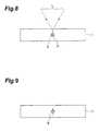
- FIG. 8is a sectional view of the object to be processed in a first step of the laser processing method in accordance with the embodiment
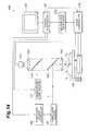
- FIG. 9is a sectional view of the object to be processed in a second step of the laser processing method in accordance with the embodiment.
- FIG. 10is a sectional view of the object to be processed in a third step of the laser processing method in accordance with the embodiment.
- FIG. 11is a sectional view of the object to be processed in a fourth step of the laser processing method in accordance with the embodiment.
- FIG. 12is a view showing a photograph of a cut section in a part of a silicon wafer cut by the laser processing method in accordance with the embodiment
- FIG. 13is a graph showing relationships between the laser light wavelength and the internal transmittance of a silicon substrate in the laser processing method in accordance with the embodiment
- FIG. 14is a schematic diagram of the laser processing apparatus in accordance with Example 1.
- FIG. 15is a flowchart for explaining the laser processing method in accordance with Example 1;
- FIG. 16is a view showing the semiconductor substrate after a step of forming a starting point region for cutting in accordance with Example 1;
- FIG. 17is a view for explaining a step of attaching a protective film in accordance with Example 1;
- FIG. 18is a view for explaining a step of grinding the semiconductor substrate in accordance with Example 1;
- FIG. 19is a view for explaining a step of attaching an expansion film in accordance with Example 1;
- FIG. 20is a view for explaining a step of peeling the protective film in accordance with Example 1;
- FIG. 21is a view for explaining a step of expanding the expansion film and picking up semiconductor chips in accordance with Example 1;
- FIG. 22is a view showing chamfers formed at edge parts on the rear face side of cut surfaces of semiconductor chips after the step of grinding the semiconductor substrate in accordance with Example 1;
- FIG. 23Ais a view for explaining a case where a molten processed region remains in a cut surface of a semiconductor chip after the step of grinding the semiconductor substrate in accordance with Example 1, while a fracture reaches the front face before the step of grinding the semiconductor substrate;
- FIG. 23Bis a view for explaining a case where a molten processed region remains in a cut surface of a semiconductor chip after the step of grinding the semiconductor substrate in accordance with Example 1, while a fracture does not reach the front face before the step of grinding the semiconductor substrate;
- FIG. 24Ais a view for explaining a case where a molten processed region does not remain in a cut surface of a semiconductor chip after the step of grinding the semiconductor substrate in accordance with Example 1, while a fracture reaches the front face before the step of grinding the semiconductor substrate;
- FIG. 24Bis a view for explaining a case where a molten processed region does not remain in a cut surface of a semiconductor chip after the step of grinding the semiconductor substrate in accordance with Example 1, while a fracture does not reach the front face before the step of grinding the semiconductor substrate;
- FIG. 25Ais a view for explaining a case where a molten processed region remains in an edge part on the rear face side of a cut surface of a semiconductor chip after the step of grinding the semiconductor substrate in accordance with Example 1, while a fracture reaches the front face before the step of grinding the semiconductor substrate;
- FIG. 25Bis a view for explaining a case where a molten processed region remains in an edge part on the rear face side of a cut surface of a semiconductor chip after the step of grinding the semiconductor substrate in accordance with Example 1, while a fracture does not reach the front face before the step of grinding the semiconductor substrate;
- FIG. 26Ais a sectional view of a marginal part of the semiconductor substrate before the step of grinding the semiconductor substrate in accordance with Example 1;
- FIG. 26Bis a sectional view of the marginal part of the semiconductor substrate after the step of grinding the semiconductor substrate in accordance with Example 1;
- FIG. 27is a plan view of the sapphire substrate in accordance with Example 2.
- FIG. 28is a sectional view for explaining a step of forming a starting point region for cutting in accordance with Example 2;
- FIG. 29is a sectional view for explaining a step of forming a functional device in accordance with Example 2.
- FIG. 30is a sectional view for explaining a step of attaching a protective film in accordance with Example 2;
- FIG. 31is a sectional view for explaining a step of grinding the sapphire substrate in accordance with Example 2;
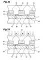
- FIG. 32is a sectional view for explaining a step of attaching an expansion film in accordance with Example 2;
- FIG. 33is a sectional view for explaining a step of irradiating the protective film with UV rays in accordance with Example 2;
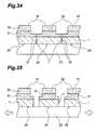
- FIG. 34is a sectional view for explaining a step of peeling the protective film in accordance with Example 2.
- FIG. 35is a sectional view for explaining a step of expanding the expansion film and separating semiconductor chips in accordance with Example 2.
- the substrate dividing method in accordance with this methodcomprises the steps of irradiating a substrate with laser light while positioning a light-converging point within the substrate, so as to form a modified region due to multiphoton absorption within the substrate, thereby forming a starting point region for cutting; and then grinding the substrate such that the substrate attains a predetermined thickness.
- the condition under which absorption occurs in the materialis h ⁇ >E G .
- the material yields absorption under the condition of nh ⁇ >E G (n2, 3, 4, . . . ) if the intensity of laser light is very high. This phenomenon is known as multiphoton absorption.
- the intensity of laser lightis determined by the peak power density (W/cm 2 ) of laser light at a light-converging point thereof.
- the multiphoton absorptionoccurs, for example, at a peak power density (W/cm 2 ) of 1 ⁇ 10 8 (W/cm 2 ) or higher.
- the peak power densityis determined by (energy per pulse of laser light at the light-converging point)/(laser light beam spot cross-sectional area ⁇ pulse width).
- the intensity of laser lightis determined by the electric field strength (W/cm 2 ) of laser light at the light-converging point.
- FIG. 1is a plan view of a substrate 1 during laser processing
- FIG. 2is a sectional view of the substrate 1 taken along the line II-II of FIG. 1
- FIG. 3is a plan view of the substrate 1 after laser processing
- FIG. 4is a sectional view of the substrate 1 taken along the line IV-IV of FIG. 3
- FIG. 5is a sectional view of the substrate 1 taken along the line V-V of FIG. 3
- FIG. 6is a plan view of the cut substrate 1 .
- the front face 3 of the substrate 1has a desirable line along which the substrate should be cut 5 for cutting the substrate 1 .
- the line along which the substrate should be cut 5is a linearly extending virtual line (the substrate 1 may also be formed with an actual line acting as the line along which the substrate should be cut 5 ).
- the substrate 1is irradiated with laser light L such that a light-converging point P is positioned within the semiconductor substrate 1 under a condition causing multiphoton absorption, so as to form a modified region 7 .
- the light-converging pointis a location where the laser light L is converged.
- the laser light Lis relatively moved along the line along which the substrate should be cut 5 (in the direction of arrow A), so as to move the light-converging point P along the line along which the substrate should be cut 5 .
- no modified region 7is formed upon heating the substrate 1 by causing the substrate 1 to absorb the laser light L.
- the laser light Lis transmitted through the semiconductor substrate 1 , so as to generate multiphoton absorption within the semiconductor substrate 1 , thereby forming the modified region 7 .
- the laser light Lis hardly absorbed by the front face 3 of the semiconductor substrate 1 , whereby the front face 3 of the semiconductor substrate 1 does not melt.
- the substrate 1fractures from this start point and thus can be cut with a relatively small force as shown in FIG. 6 . This makes it possible to cut the substrate 1 without generating unnecessary fractures in the front face 3 of the substrate 1 .
- the first caseis where, after forming the starting point region for cutting, an artificial force is applied to the substrate, so that the substrate fractures from the starting point region for cutting acting as a start point, whereby the substrate is cut.
- Thisis the cutting in the case where the substrate has a large thickness, for example.
- the application of an artificial forceencompasses application of bending stress and shearing stress along the starting point region for cutting of the substrate, and exertion of a temperature difference upon the substrate to generate thermal stress, for example.
- the other caseis where a starting point region for cutting is formed, so that the substrate is naturally fractured in a cross-sectional direction (thickness direction) of the substrate from the starting point region for cutting acting as a start point, whereby the substrate is cut.
- Thisis enabled, for example, by forming the starting point region for cutting by a single row of modified regions when the substrate has a small thickness, and by a plurality of rows of modified regions aligned in the thickness direction when the substrate has a large thickness.
- fracturesdo not extend to the front face at a location not formed with the starting point region for cutting in the part to cut, whereby only the part corresponding to the location formed with the starting point region for cutting can be fractured.
- fracturingcan be regulated well.
- Such a fracturing method with favorable controllabilityis quite effective, since semiconductor substrates such as silicon wafers have recently been apt to become thinner.
- the modified region formed by multiphoton absorption in this embodimentincludes the following cases (1) to (3):
- a substratee.g., glass or a piezoelectric material made of LiTaO 3
- a substrateis irradiated with laser light while a light-converging point is positioned therewithin under a condition with an electric field intensity of at least 1 ⁇ 10 8 (W/cm 2 ) at the light-converging point and a pulse width of 1 ⁇ s or less.
- This pulse widthis a condition under which a crack region can be formed only within the substrate while generating multiphoton absorption without causing unnecessary damages to the substrate. This generates a phenomenon of optical damage due to multiphoton absorption within the substrate. This optical damage induces thermal distortion within the substrate, thereby forming a crack region therewithin.
- the upper limit of electric field intensityis 1 ⁇ 10 12 (W/cm 2 ), for example.
- the pulse widthis preferably 1 ns to 200 ns, for example.
- the forming of a crack region due to multiphoton absorptionis described, for example, in “Internal Marking of Glass Substrate by Solid-state Laser Harmonics”, Proceedings of 45th Laser Materials Processing Conference (December 1998), pp. 23-28.
- the inventorsdetermined relationships between the electric field intensity and the magnitude of crack by an experiment. Conditions for the experiment are as follows:
- SubstratePyrex (registered trademark) glass (having a thickness of 700 ⁇ m)
- the laser light quality being TEM 00indicates that the light convergence is so high that light can be converged up to about the wavelength of laser light.
- FIG. 7is a graph showing the results of the above-mentioned experiment.
- the abscissaindicates peak power density. Since laser light is pulse laser light, its electric field intensity is represented by the peak power density.
- the ordinateindicates the size of a crack part (crack spot) formed within the substrate processed by one pulse of laser light. Crack spots gather, so as to form a crack region.
- the size of a crack spotrefers to that of the part of dimensions of the crack spot yielding the maximum length.
- the data indicated by black circles in the graphrefers to a case where the light-converging lens (C) has a magnification of ⁇ 100 and a numerical aperture (NA) of 0.80.
- the data indicated by white circles in the graphrefers to a case where the light-converging lens (C) has a magnification of ⁇ 50 and a numerical aperture (NA) of 0.55. It is seen that crack spots begin to occur within the substrate when the peak power density reaches about 10 11 (W/cm 2 ), and become greater as the peak power density increases.
- the substrate 1is irradiated with laser light L while positioning the light-converging point P within the substrate 1 under a condition where multiphoton absorption occurs, so as to form a crack region 9 therewithin along a line along which the substrate should be cut.
- the crack region 9is a region including one or a plurality of crack spots.
- the crack region 9forms a starting point region for cutting.
- the crackfurther grows while using the crack region 9 as a start point (i.e., using the starting point region for cutting as a start point). As shown in FIG.
- the crackreaches the front face 3 and rear face 21 of the substrate 1 .
- the substrate 1breaks, so as to be cut.
- the crack reaching the front face and rear face of the substratemay grow naturally or grow as a force is applied to the substrate.
- a substratee.g., a semiconductor material such as silicon
- a light-converging pointis positioned therewithin under a condition with an electric field intensity of at least 1 ⁇ 10 8 (W/cm 2 ) at the light-converging point and a pulse width of 1 ⁇ s or less.
- the inside of the substrateis locally heated by multiphoton absorption. This heating forms a molten processed region within the substrate.
- the molten processed regionrefers to a region once melted and then re-solidified, a region just in a melted state, or a region in the process of re-solidifying from its melted state, and may also be defined as a phase-changed region or a region having changed its crystal structure.
- the molten processed regionmay also be regarded as a region in which a certain structure has changed into another structure in monocrystal, amorphous, and polycrystal structures.
- the molten processed regionis an amorphous silicon structure, for example.
- the upper limit of electric field intensityis 1 ⁇ 10 12 (W/cm 2 ), for example.
- the pulse widthis preferably 1 ns to 200 ns, for example.
- Substratesilicon wafer (having a thickness of 350 ⁇ m and an outer diameter of 4 inches)
- FIG. 12is a view showing a photograph of a cut section in a part of a silicon wafer cut by laser processing under the above-mentioned conditions.
- a molten processed region 13is formed within a silicon wafer 11 .
- the size of the molten processed region 13 formed under the above-mentioned conditionsis about 100 ⁇ m in the thickness direction.
- FIG. 13is a graph showing relationships between the wavelength of laser light and the transmittance within the silicon substrate.
- respective reflecting components on the front face side and rear face side of the silicon substrateare eliminated, whereby only the transmittance therewithin is represented.
- the above-mentioned relationshipsare shown in the cases where the thickness t of the silicon substrate is 50 ⁇ m, 100 ⁇ m, 200 ⁇ m, 500 ⁇ m, and 1000 ⁇ m, respectively.
- laser lighttransmits through the silicon substrate by at least 80% at 1064 nm, where the wavelength of Nd:YAG laser is located, when the silicon substrate has a thickness of 500 ⁇ m or less.
- the silicon wafer 11 shown in FIG. 12has a thickness of 350 ⁇ m
- the molten processed region 13 due to multiphoton absorptionis formed near the center of the silicon wafer, i.e., at a part separated from the front face by 175 ⁇ m.
- the transmittance in this caseis 90% or greater with reference to a silicon wafer having a thickness of 200 ⁇ m, whereby the laser light is absorbed within the silicon wafer 11 only slightly and is substantially transmitted therethrough.
- the molten processed region 13is not formed by laser light absorption within the silicon wafer 11 (i.e., not formed upon usual heating with laser light), but by multiphoton absorption.
- the forming of a molten processed region by multiphoton absorptionis described, for example, in “Processing Characteristic Evaluation of Silicon by Picosecond Pulse Laser”, Preprints of the National Meeting of Japan Welding Society, No. 66 (April 2000), pp. 72-73.
- a fractureis generated in the cross-sectional direction while using a molten processed region as a start point, whereby the silicon wafer is cut when the fracture reaches the front face and rear face of the silicon wafer.
- the fracture reaching the front face and rear face of the silicon wafermay grow naturally or grow as a force is applied to the silicon wafer.
- the fracturenaturally grows from the starting point region for cutting to the front face and rear face of the silicon wafer in any of the cases where the fracture grows from the molten processed region in a melted state and where the fracture grows from the molten processed region in the process of re-solidifying from the melted state. In any of these cases, the molten processed region is formed only within the silicon wafer.
- the molten processed regionis formed only therewithin as shown in FIG. 12 .
- unnecessary fractures deviating from a line along which the substrate should be cutare hard to occur at the time of fracturing, which makes it easier to control the fracturing.
- a substratee.g., glass
- a light-converging pointis positioned therewithin under a condition with an electric field intensity of at least 1 ⁇ 10 8 (W/cm 2 ) at the light-converging point and a pulse width of 1 ns or less.
- an electric field intensityof at least 1 ⁇ 10 8 (W/cm 2 ) at the light-converging point and a pulse width of 1 ns or less.
- the pulse widthis preferably 1 ns or less, more preferably 1 ps or less, for example.
- the forming of a refractive index change region by multiphoton absorptionis described, for example, in “Formation of Photoinduced Structure within Glass by Femtosecond Laser Irradiation”, Proceedings of 42th Laser Materials Processing Conference (November 1997), pp. 105-111.
- the starting point region for cuttingis preferably formed in a direction along the (111) plane (first cleavage plane) or (110) plane (second cleavage plane).
- the starting point region for cuttingis preferably formed in a direction along the (110) plane.
- a starting point region for cuttingis preferably formed in a direction along the (1120) plane (A plane) or (1100) plane (M plane) while using the (0001) plane (C plane) as a principal plane.
- the starting point region for cuttingextending along the direction to be formed with the starting point region for cutting can be formed in the substrate in an easy and accurate manner with reference to the orientation flat.
- Example 1 of the substrate dividing method in accordance with the present inventionwill now be explained.
- Example 1is directed to a case where the substrate 1 is a silicon wafer (having a thickness of 350 ⁇ m and an outer diameter of 4 inches) (“substrate 1 ” will hereinafter be referred to as “semiconductor substrate 1 ” in Example 1), whereas the front face 3 of the semiconductor substrate 1 is formed with a plurality of functional devices in a device manufacturing process.
- FIG. 14is a schematic diagram of the laser processing apparatus 100 .
- the laser processing apparatus 100comprises a laser light source 101 for generating laser light L; a laser light source controller 102 for controlling the laser light source 101 so as to regulate the output, pulse width, etc. of laser light L and the like; a dichroic mirror 103 , arranged so as to change the orientation of the optical axis of laser light L by 90°, having a function of reflecting the laser light L; a light-converging lens 105 for converging the laser light L reflected by the dichroic mirror 103 ; a mounting table 107 for mounting a semiconductor substrate 1 irradiated with the laser light L converged by the light-converging lens 105 ; an X-axis stage 109 for moving the mounting table 107 in the X-axis direction; a Y-axis stage 111 for moving the mounting table 107 in the Y-axis direction orthogonal to the X-axis direction; a Z-axis stage 113 for moving the mounting table 107 in the Z-axis direction orthogonal to
- the Z-axis directionis a direction orthogonal to the front face 3 of the semiconductor substrate 1 , and thus becomes the direction of focal depth of laser light L incident on the semiconductor substrate 1 . Therefore, moving the Z-axis stage 113 in the Z-axis direction can position the light-converging point P of laser light L within the semiconductor substrate 1 .
- This movement of light-converging point P in X(Y)-axis directionis effected by moving the semiconductor substrate 1 in the X(Y)-axis direction by the X(Y)-axis stage 109 (111).
- the laser light source 101is an Nd:YAG laser generating pulse laser light.
- Known as other kinds of laser usable as the laser light source 101include Nd:YVO 4 laser, Nd:YLF laser, and titanium sapphire laser.
- Nd:YAG laser, Nd:YVO 4 laser, and Nd:YLF laserare preferably employed.
- pulse laser lightis used for processing the semiconductor substrate 1 in Example 1, continuous wave laser light may be used as long as it can cause multiphoton absorption.
- the laser processing apparatus 100further comprises an observation light source 117 for generating a visible light beam for irradiating the semiconductor substrate 1 mounted on the mounting table 107 , and a visible light beam splitter 119 disposed on the same optical axis as that of the dichroic mirror 103 and light-converging lens 105 .
- the dichroic mirror 103is disposed between the beam splitter 119 and light-converging lens 105 .
- the beam splitter 119has a function of reflecting about a half of a visual light beam and transmitting the remaining half therethrough, and is arranged so as to change the orientation of the optical axis of the visual light beam by 90°.
- the laser processing apparatus 100further comprises an image pickup device 121 and an imaging lens 123 which are disposed on the same optical axis as that of the beam splitter 119 , dichroic mirror 103 , and light-converging lens 105 .
- An example of the image pickup device 121is a CCD camera.
- the reflected light of the visual light beam having illuminated the front face 3 including the line along which the substrate should be cut 5 and the likeis transmitted through the light-converging lens 105 , dichroic mirror 103 , and beam splitter 119 and forms an image by way of the imaging lens 123 , whereas thus formed image is captured by the image pickup device 121 , so as to yield imaging data.
- the laser processing apparatus 100further comprises an imaging data processor 125 for inputting the imaging data outputted from the image pickup device 121 , an overall controller 127 for controlling the laser processing apparatus 100 as a whole, and a monitor 129 .
- the imaging data processor 125calculates focal point data for positioning the focal point of the visible light generated from the observation light source 117 onto the front face 3 .
- the stage controller 115controls the movement of the Z-axis stage 113 , so that the focal point of visible light is positioned on the front face 3 .
- the imaging data processor 125functions as an autofocus unit.
- the imaging data processor 125calculates image data such as an enlarged image of the front face 3 .
- the image datais sent to the overall controller 127 , subjected to various kinds of processing therein, and then sent to the monitor 129 . As a consequence, an enlarged image or the like is displayed on the monitor 129 .
- the overall controller 127regulates the laser light source controller 102 , observation light source 117 , and stage controller 115 , thereby controlling the laser processing apparatus 100 as a whole.
- the overall controller 127functions as a computer unit.
- FIG. 15is a flowchart for explaining the step of forming a starting point region for cutting.
- Light absorption characteristics of the semiconductor substrate 1are determined by a spectrophotometer or the like which is not depicted. According to the results of measurement, a laser light source 101 generating laser light L having a wavelength to which the semiconductor substrate 1 is transparent or exhibits a low absorption is chosen (S 101 ). Subsequently, the thickness of the semiconductor substrate 1 is measured. According to the result of measurement of thickness and the refractive index of the semiconductor substrate 1 , the amount of movement of the semiconductor substrate 1 in the Z-axis direction is determined (S 103 ).
- This amount of movementis fed into the overall controller 127 .
- the semiconductor substrate 1is mounted on the mounting table 107 of the laser processing apparatus 100 . Subsequently, visible light is generated from the observation light source 117 , so as to illuminate the semiconductor substrate 1 (S 105 ).
- the illuminated front face 3 of the semiconductor substrate 1 including the line along which the substrate should be cut 5is captured by the image pickup device 121 .
- the line along which the substrate should be cut 5is a desirable virtual line for cutting the semiconductor substrate 1 .
- the line along which the substrate should be cut 5is set like a grid running between the functional devices adjacent each other.
- the imaging data captured by the imaging device 121is sent to the imaging data processor 125 . According to the imaging data, the imaging data processor 125 calculates such focal point data that the focal point of visible light from the observation light source 117 is positioned at the front face 3 (S 107 ).
- the focal point datais sent to the stage controller 115 .
- the stage controller 115moves the Z-axis stage 113 in the Z-axis direction (S 109 ).
- the focal point of visible light from the observation light source 117is positioned at the front face 3 of the semiconductor substrate 1 .
- the imaging data processor 125calculates enlarged image data of the front face 3 of the semiconductor substrate 1 including the line along which the substrate should be cut 5 .
- the enlarged image datais sent to the monitor 129 by way of the overall controller 127 , whereby an enlarged image of the line along which the substrate should be cut 5 and its vicinity is displayed on the monitor 129 .
- Movement amount data determined in step S 103has been fed into the overall controller 127 beforehand, and is sent to the stage controller 115 .
- the stage controller 115causes the Z-axis stage 113 to move the substrate 1 in the Z-axis direction to a position where the converging point P of laser light L is positioned within the light-semiconductor substrate 1 (S 111 ).
- laser light Lis generated from the laser light source 101 , so as to irradiate the line along which the substrate should be cut 5 in the front face 3 of the semiconductor substrate 1 .
- the X-axis stage 109 and Y-axis stage 111are moved along the line along which the substrate should be cut 5 , so as to form a molten processed region along the line along which the substrate should be cut 5 , thereby forming a starting point region for cutting within the semiconductor substrate 1 along the line along which the substrate should be cut 5 (S 113 ).
- the foregoingcompletes the step of forming a starting point region for cutting, thereby forming the starting point region for cutting within the semiconductor substrate 1 .
- a fractureis generated in the thickness direction of the semiconductor substrate 1 from the starting point region for cutting acting as a start point naturally or with a relatively small force exerted thereon.
- Example 1the starting point region for cutting is formed at a position near the front face 3 side within the semiconductor substrate 1 in the above-mentioned step of forming a starting point region for cutting, and a fracture is generated in the thickness direction of the semiconductor substrate 1 from the starting point region for cutting acting as a start point.
- FIG. 16is a view showing the semiconductor substrate 1 after the starting point region for cutting is formed.
- fractures 15 generated from the starting point region for cutting acting as a start pointare formed like a grid along lines to cut, and reach only the front face 3 of the semiconductor substrate 1 but not the rear face 21 thereof.
- the fractures 15 generated in the semiconductor substrate 1separate a plurality of functional devices 19 formed like a matrix on the front face of the semiconductor substrate 1 from each other.
- the cut surfaces of the semiconductor substrate 1 cut by the fractures 15are in close contact with each other.
- the starting point region for cuttingis formed at a position near the front face 3 side within the semiconductor substrate 1
- a modified regionsuch as a molten processed region constituting a starting point region for cutting is formed so as to shift from the center position in the thickness direction of the semiconductor substrate 1 (i.e., half thickness position) toward the front face 3 .
- itrefers to a case where the center position of the width of the modified region in the thickness direction of the semiconductor substrate 1 is shifted toward the front face 3 from the center position in the thickness direction of the semiconductor substrate 1 , and is not limited to the case where the whole modified region is located on the front face 3 side from the center position in the thickness direction of the semiconductor substrate 1 .
- FIGS. 17 to 21are views for explaining respective steps including the step of grinding the semiconductor substrate.
- the semiconductor substrate 1is thinned from the thickness of 350 ⁇ m to a thickness of 50 ⁇ m.
- a protective film 20is attached to the front face 3 of the semiconductor substrate after the starting point region for cutting is formed.
- the protective film 20is used for protecting the functional devices 19 formed on the front face 3 of the semiconductor substrate 1 and holding the semiconductor substrate 1 .
- the rear face 21 of the semiconductor substrate 1is subjected to surface grinding and then chemical etching, whereby the semiconductor substrate 1 is thinned to the thickness of 50 ⁇ m.
- the rear face 21reaches the fractures 15 generated from the starting point region for cutting acting as a start point, whereby the semiconductor substrate 1 is divided into semiconductor chips 25 having the respective functional devices 19 .
- the chemical etchinginclude wet etching (HF.HNO 3 ) and plasma etching (HBr.Cl 2 ).
- an expansion film 23is attached so as to cover the rear faces of all the semiconductor chips 25 .
- the protective film 20 attached so as to cover the functional devices of all the semiconductor chips 25are peeled off.
- the expansion film 23is expanded, so that the semiconductor chips 25 are separated from each other, and a suction collet 27 picks up the semiconductor chips 25 .
- the substrate dividing method in accordance with Example 1can grind the rear face 21 of the semiconductor substrate 1 after forming the functional devices 19 on the front face 3 of the semiconductor substrate 1 in the device manufacturing process. Also, because of the following effects respectively exhibited by the step of forming a starting point region for cutting and the step of grinding the semiconductor substrate, the semiconductor chips 25 thinned so as to respond to the smaller size of semiconductor devices can be obtained with a favorable yield.
- the step of forming a starting point region for cuttingcan prevent unnecessary fractures and melting deviated from a desirable line along which the substrate should be cut for cutting the semiconductor substrate 1 from occurring, and thus can keep unnecessary fractures and melting from occurring in the semiconductor chips 25 obtained by dividing the semiconductor substrate 1 .
- the step of forming a starting point region for cuttingdoes not melt the front face 3 of the semiconductor substrate 1 along the line along which the substrate should be cut, and thus can narrow the gap between the functional devices 19 adjacent each other, thereby making it possible to increase the number of semiconductor chips 25 separated from one semiconductor substrate 1 .
- the step of grinding the semiconductor substratesubjects the rear face 21 of the semiconductor substrate 1 to surface grinding such that the semiconductor substrate 1 attains a predetermined thickness after the starting point region for cutting is formed within the semiconductor substrate 1 .
- the rear face 21reaches the fractures 15 generated from the starting point region for cutting acting as a start point, the cut surfaces of the semiconductor substrate 1 cut by the fractures 15 are in close contact with each other, whereby the semiconductor substrate 1 can be prevented from chipping and cracking because of the surface grinding. Therefore, the semiconductor substrate 1 can be made thinner and divided while preventing the chipping and cracking from occurring.
- the close contact of the cut surfaces in the semiconductor substrate 1is also effective in preventing the grinding dust caused by the surface grinding from entering the fractures 15 , and keeping the semiconductor chips 25 obtained by dividing the semiconductor substrate 1 from being contaminated with the grinding dust.
- the close contact of the cut surfaces in the semiconductor substrate 1is effective in reducing the chip-off of the semiconductor chips 25 caused by the surface grinding as compared with the case where the semiconductor chips 25 are separated from each other. Namely, as the protective film 20 , one with a low holding power can be used.
- the rear faces of the semiconductor chips 25 obtained by dividing the semiconductor substrate 1can be made smoother. Further, since the cut surfaces of the semiconductor substrate 1 caused by the fractures 15 generated from the starting point region for cutting acting as a start point are in close contact with each other, only edge parts of the cut surfaces on the rear face side are selectively etched as shown in FIG. 22 , whereby chamfers 29 are formed. Therefore, the transverse rupture strength of the semiconductor chips 25 obtained by dividing the semiconductor substrate 1 can be improved, and the chipping and cracking in the semiconductor chips 25 can be prevented from occurring.
- FIGS. 23A , 24 A, and 25 Ashow the case where the fracture 15 reaches the front face 3 of the semiconductor substrate 1 before the step of grinding the semiconductor substrate
- FIGS. 23B , 24 B, and 25 Bshow the case where the fracture 15 does not reach the front face 3 of the semiconductor substrate 1 before the step of grinding the semiconductor substrate.
- FIGS. 23B , 24 B, and 25 Bshow the case where the fracture 15 does not reach the front face 3 of the semiconductor substrate 1 before the step of grinding the semiconductor substrate.
- the fracture 15reaches the front face 3 of the semiconductor substrate 1 after the step of grinding the semiconductor substrate.
- the cut surfaceis protected by the molten processed region 13 , whereby the transverse rupture strength of the semiconductor chip 25 improves.
- the semiconductor chip 25 in which the molten processed region 13 does not remain within the cut surface as shown in FIGS. 24A and 24Bis effective in the case where the molten processed region 13 does not favorably influence the semiconductor device.
- the edge partis protected by the molten processed region 13 , whereby the chipping and cracking in the edge part can be prevented from occurring as in the case where the edge part of the semiconductor chip 25 is chamfered.
- the rectilinearity of the cut surface obtained after the step of grinding the semiconductor substrateimproves more in the case where the fracture 15 does not reach the front face 3 of the semiconductor substrate 1 before the step of grinding the semiconductor substrate as shown in FIGS. 23B , 24 B, and 25 B than in the case where the fracture 15 reaches the front face 3 of the semiconductor substrate 1 before the step of grinding the semiconductor substrate as shown in FIGS. 23A , 24 A, and 25 A.
- the fracture reaches the front face 3 of the semiconductor substrate 1 or notdepends on not only the depth of the molten processed region 13 from the front face 3 , but also the size of the molten processed region 13 . Namely, when the molten processed region 13 is made smaller, the fracture 15 does not reach the front face 3 of the semiconductor substrate 1 even if the depth of the molten processed region 13 from the front face 3 is small.
- the size of the molten processed region 13can be controlled by the output of the pulse laser light in the step of forming a starting point region for cutting, for example, and becomes greater and smaller as the output of the pulse laser light is higher and lower, respectively.
- FIGS. 26A and 26Bare respective sectional views of a marginal part of the semiconductor substrate 1 before and after the step of grinding the semiconductor substrate in accordance with Example 1.
- the thickness of the semiconductor 1 shown in FIG. 26A before the step of grinding the semiconductor substrateis 350 ⁇ m
- the thickness of the semiconductor 1 shown in FIG. 26B after the step of grinding the semiconductor substrateis 50 ⁇ m. As shown in FIG.
- a plurality of (seven here) rounded portionsare formed at the marginal part of the semiconductor substrate 1 beforehand by chamfering with a thickness of 50 ⁇ m each, i.e., the marginal part of the semiconductor substrate 1 is caused to have a wavy form.
- the marginal part of the semiconductor substrate 1 after the step of grinding the semiconductor substrate 1attains a state rounded by chamfering as shown in FIG. 26B , whereby the chipping and cracking can be prevented from occurring at the marginal part, and handling can be made easier because of an improvement in mechanical strength.
- Example 2 of the substrate dividing method in accordance with the present inventionwill now be explained with reference to FIGS. 27 to 35 .
- Example 2relates to a case where the substrate 1 is a sapphire substrate (having a thickness of 450 ⁇ m and an outer diameter of 2 inches) which is an insulating substrate (“substrate 1 ” will hereinafter be referred to as “sapphire substrate 1 ” in Example 2), so as to yield a semiconductor chip to become a light-emitting diode.
- FIGS. 28 to 35are sectional views of the sapphire substrate 1 taken along the line XX-XX of FIG. 27 .
- the sapphire substrate 1is irradiated with laser light L while a light-converging point P is positioned therewithin, so as to form a modified region 7 within the sapphire substrate 1 .
- a plurality of functional devices 19are formed like a matrix on the front face 3 of the sapphire substrate 1 , and the sapphire substrate 1 is divided into the functional devices 19 . Therefore, lines to cut are formed like a grid in conformity to the size of each functional device 19 as seen from the front face 3 side, modified regions 7 are formed along the lines to cut, and the modified regions 7 are used as starting point regions for cutting.
- the sapphire substrate 1When the sapphire substrate 1 is irradiated with laser light under a condition with an electric field intensity of at least 1 ⁇ 10 8 (W/cm 2 ) at the light-converging point P and a pulse width of 1 ⁇ s or less, a crack region is formed as the modified region 7 (there is also a case where a molten processed region is formed).
- the (0001) plane of the sapphire substrate 1is employed as the front face 3 , and a modified region 7 is formed in a direction along the (1120) plane and a direction orthogonal thereto, the substrate can be cut by a smaller force with a favorable accuracy from the starting point region for cutting formed by the modified region 7 as a start point. The same holds when a modified region 7 is formed in a direction along the (1100) plane and a direction orthogonal thereto.
- n-type layer 31is grown as a crystal until its thickness becomes 6 ⁇ m on the front face 3 of the sapphire substrate 1
- p-type layer 32is grown as a crystal until its thickness becomes 1 ⁇ m on the n-type layer 31 .
- the n-type layer 31 and p-type layer 32are etched to the middle of the n-type layer 31 along the modified regions 7 formed like a grid, so as to form a plurality of functional devices 19 made of the n-type layer 31 and p-type layer 32 into a matrix.
- the sapphire substrate 1may be irradiated with laser light L while the light-converging point P is positioned therewithin, so as to form the modified regions 7 within the sapphire substrate 1 .
- the sapphire substrate 1may be irradiated with the laser light L from the front face 3 side or rear face 21 side.
- the n-type layer 31 and p-type layer 32can be prevented from melting, since the laser light L is transmitted through the sapphire substrate 1 , n-type layer 31 , and p-type layer 32 .
- a protective film 20is attached to the front face 3 side of the sapphire substrate 1 .
- the protective film 20is used for protecting the functional devices 19 formed on the front face 3 of the semiconductor substrate 1 and holding the sapphire substrate 1 .
- the rear face 21 of the sapphire substrate 1is subjected to surface grinding, so that the sapphire substrate 1 is thinned to the thickness of 150 ⁇ m.
- the grinding of the rear face 21 of the sapphire substrate 1generates a fracture 15 from a starting point region for cutting formed by the modified region 7 as a start point. This fracture 15 reaches the front face 3 and rear face 21 of the sapphire substrate 1 , whereby the sapphire substrate 1 is divided into semiconductor chips 35 each having the functional device 19 constituted by the n-type layer 31 and p-type layer 32 .
- an expandable expansion film 23is attached so as to cover the rear faces of all the semiconductor chips 25 as shown in FIG. 32 , and then the protective film 20 is irradiated with UV rays as shown in FIG. 33 , so as to cure a UV curable resin which is an adhesive layer of the protective film 20 . Thereafter, the protective film 20 is peeled off as shown in FIG. 34 . Subsequently, as shown in FIG. 35 , the expansion film 23 is expanded outward, so as to separate the semiconductor chips 25 from each other, and the semiconductor chips 25 are picked up by a suction collet or the like. Thereafter, electrodes are attached to the n-type layer 31 and p-type layer 32 of the semiconductor chip 25 , so as to make a light-emitting diode.
- the sapphire substrate 1is irradiated with the laser light L while the light-converging point P is positioned therewithin, so as to form a modified region 7 by generating a phenomenon of multiphoton absorption, whereby the modified region 7 can form a starting point region for cutting within the sapphire substrate 1 along a desirable line along which the substrate should be cut for cutting the sapphire substrate 1 .
- a fracture 15is generated in the thickness direction of the sapphire substrate 1 from the starting point region for cutting acting as a start point naturally or with a relatively small force exerted thereon.
- the sapphire substrate 1is ground so as to attain a predetermined thickness after a starting point region for cutting is formed within the sapphire substrate 1 .
- the ground surfacereaches the fracture 15 generated from the starting point region for cutting acting as a start point, the cut surfaces of the sapphire substrate 1 cut by the fracture 15 are in close contact with each other, whereby the sapphire substrate 1 can be prevented from chipping and cracking upon grinding.
- the sapphire substrate 1can be thinned and divided while preventing the chipping and cracking from occurring, whereby semiconductor chips 25 with the thinned sapphire substrate 1 can be obtained with a favorable yield.
- the present inventioncan thin and divide the substrate while preventing the chipping and cracking from occurring.
Landscapes
- Engineering & Computer Science (AREA)
- Physics & Mathematics (AREA)
- Optics & Photonics (AREA)
- Microelectronics & Electronic Packaging (AREA)
- Condensed Matter Physics & Semiconductors (AREA)
- Computer Hardware Design (AREA)
- General Physics & Mathematics (AREA)
- Power Engineering (AREA)
- Mechanical Engineering (AREA)
- Manufacturing & Machinery (AREA)
- Plasma & Fusion (AREA)
- Chemical Kinetics & Catalysis (AREA)
- General Chemical & Material Sciences (AREA)
- Chemical & Material Sciences (AREA)
- High Energy & Nuclear Physics (AREA)
- Oil, Petroleum & Natural Gas (AREA)
- Electromagnetism (AREA)
- Health & Medical Sciences (AREA)
- Toxicology (AREA)
- Laser Beam Processing (AREA)
- Dicing (AREA)
- Processing Of Stones Or Stones Resemblance Materials (AREA)
- Re-Forming, After-Treatment, Cutting And Transporting Of Glass Products (AREA)
- Crystals, And After-Treatments Of Crystals (AREA)
Abstract
Description
This is a continuation application of copending application Ser. No. 10/507,321, filed on Jun. 28, 2005, which is the National Stage of International Application No. PCT/JP03/02669 filed Mar. 6, 2003, designating the U.S.A., the entire contents of each of which are incorporated herein in their entirety.
The present invention relates to a substrate dividing method used for dividing a substrate such as a semiconductor substrate in a step of making a semiconductor device or the like.
As semiconductor devices have been becoming smaller in recent years, there are cases where a semiconductor substrate is thinned to a thickness of several tens of micrometers in a step of making a semiconductor device. When thus thinned semiconductor substrate is cut and divided by a blade, chipping and cracking occur more than in the case where a semiconductor substrate is thicker, thereby causing a problem that the yield of semiconductor chips obtained by dividing the semiconductor substrate decreases.
Known as semiconductor substrate dividing methods which can solve such a problem are those described in Japanese Patent Application Laid-Open Nos. SHO 64-38209 and SHO 62-4341.
In the methods described in these publications, a semiconductor substrate having a front face formed with a functional device is inscribed with a groove by a blade on the front face side, then an adhesive sheet is attached to the front face, so as to hold the semiconductor substrate, and the rear face of the semiconductor substrate is ground until the groove formed beforehand is exposed, thereby thinning the semiconductor substrate and dividing the semiconductor substrate.
If the grinding of the rear face of the semiconductor substrate is performed by surface grinding in the methods described in the above-mentioned publications, however, chipping and cracking may occur at side faces of the groove formed beforehand in the semiconductor substrate when the surface-ground face reaches the groove.
In view of such a circumstance, it is an object of the present invention to provide a substrate dividing method which can prevent chipping and cracking from occurring, and thin and divide a substrate.
For achieving the above-mentioned object, the substrate dividing method in accordance with the present invention comprises the steps of irradiating a substrate with laser light while positioning a light-converging point within the substrate, so as to form a modified region due to multiphoton absorption within the substrate, and causing the modified region to form a starting point region for cutting along a line along which the substrate should be cut in the substrate inside by a predetermined distance from a laser light incident face of the substrate; and grinding the substrate after the step of forming the starting point region for cutting such that the substrate attains a predetermined thickness.
Since this substrate dividing method irradiates the substrate with laser light while positioning a light-converging point within the substrate in the step of forming a starting point region for cutting, so as to generate a phenomenon of multiphoton absorption within the substrate, thereby forming a modified region, this modified region can form a starting point region for cutting within the substrate along a desirable line along which the substrate should be cut for cutting the substrate. When a starting point region for cutting is formed within the substrate, a fracture is generated in the substrate in its thickness direction from the starting point region for cutting acting as a start point naturally or with a relatively small force exerted thereon.
In the step of grinding the substrate, the substrate is ground such that the substrate attains a predetermined thickness after the starting point region for cutting is formed within the substrate. Here, even when the ground surface reaches the fracture generated from the starting point region for cutting acting as a start point, cut surfaces of the substrate cut by the fracture remain in close contact with each other, whereby the substrate can be prevented from chipping and cracking upon grinding.
This can prevent chipping and cracking from occurring, and can thin and divide the substrate.
Here, the light-converging point refers to a location at which laser light is converged. The grinding encompasses shaving, polishing, chemical etching, and the like. The starting point region for cutting refers to a region to become a start point for cutting when the substrate is cut. Therefore, the starting point region for cutting is a part to cut where cutting is to be performed in the substrate. The starting point region for cutting may be produced by continuously forming a modified region or intermittently forming a modified region.
The substrate encompasses semiconductor substrates such as silicon substrates and GaAs substrates, and insulating substrates such as sapphire substrates and AIN substrates. When the substrate is a semiconductor substrate, an example of the modified region is a molten processed region.
Preferably, a front face of the substrate is formed with a functional device, and a rear face of the substrate is ground in the step of grinding the substrate. Since the substrate can be ground after forming the functional device, a chip thinned so as to conform to a smaller size of a semiconductor device, for example, can be obtained. Here, the functional device refers to light-receiving devices such as photodiodes, light-emitting devices such as laser diodes, circuit devices formed as circuits, etc.
Preferably, the step of grinding the substrate includes a step of subjecting the rear face of the substrate to chemical etching. When the rear face of the substrate is subjected to chemical etching, the rear face of the substrate becomes smoother as a matter of course. Also, since the cut surfaces of the substrate cut by the fracture generated from the starting point region for cutting acting as a start point remain in close contact with each other, only edge parts on the rear face of the cut surfaces are selectively etched, so as to be chamfered. This can improve the transverse rupture strength of chips obtained by dividing the substrate, and prevent chipping and cracking from occurring in the chips.
In the following, a preferred embodiment of the present invention will be explained in detail with reference to drawings. The substrate dividing method in accordance with this method comprises the steps of irradiating a substrate with laser light while positioning a light-converging point within the substrate, so as to form a modified region due to multiphoton absorption within the substrate, thereby forming a starting point region for cutting; and then grinding the substrate such that the substrate attains a predetermined thickness.
First, a laser processing method carried out in the step of forming the starting point region for cutting, multiphoton absorption in particular, will be explained.
A material becomes optically transparent if its absorption bandgap EGis greater than a photon energy hν. Hence, the condition under which absorption occurs in the material is hν>EG. However, even when optically transparent, the material yields absorption under the condition of nhν>EG(n=2, 3, 4, . . . ) if the intensity of laser light is very high. This phenomenon is known as multiphoton absorption. In the case of pulse waves, the intensity of laser light is determined by the peak power density (W/cm2) of laser light at a light-converging point thereof. The multiphoton absorption occurs, for example, at a peak power density (W/cm2) of 1×10⁸(W/cm2) or higher. The peak power density is determined by (energy per pulse of laser light at the light-converging point)/(laser light beam spot cross-sectional area×pulse width). In the case of a continuous wave, the intensity of laser light is determined by the electric field strength (W/cm2) of laser light at the light-converging point.
The principle of laser processing in accordance with the embodiment utilizing such multiphoton absorption will now be explained with reference toFIGS. 1 to 6 .FIG. 1 is a plan view of asubstrate 1 during laser processing;FIG. 2 is a sectional view of thesubstrate 1 taken along the line II-II ofFIG. 1 ;FIG. 3 is a plan view of thesubstrate 1 after laser processing;FIG. 4 is a sectional view of thesubstrate 1 taken along the line IV-IV ofFIG. 3 ;FIG. 5 is a sectional view of thesubstrate 1 taken along the line V-V ofFIG. 3 ; andFIG. 6 is a plan view of thecut substrate 1.
As shown inFIGS. 1 and 2 , thefront face 3 of thesubstrate 1 has a desirable line along which the substrate should be cut5 for cutting thesubstrate 1. The line along which the substrate should be cut5 is a linearly extending virtual line (thesubstrate 1 may also be formed with an actual line acting as the line along which the substrate should be cut5). In the laser processing in accordance with this embodiment, thesubstrate 1 is irradiated with laser light L such that a light-converging point P is positioned within thesemiconductor substrate 1 under a condition causing multiphoton absorption, so as to form a modifiedregion 7. Here, the light-converging point is a location where the laser light L is converged.
The laser light L is relatively moved along the line along which the substrate should be cut5 (in the direction of arrow A), so as to move the light-converging point P along the line along which the substrate should be cut5. This forms the modifiedregion 7 along the line along which the substrate should be cut5 only within thesubstrate 1 as shown inFIGS. 3 to 5 , and the modifiedregion 7 forms a starting point region for cutting (part to cut)8. In the laser processing method in accordance with this embodiment, no modifiedregion 7 is formed upon heating thesubstrate 1 by causing thesubstrate 1 to absorb the laser light L. Instead, the laser light L is transmitted through thesemiconductor substrate 1, so as to generate multiphoton absorption within thesemiconductor substrate 1, thereby forming the modifiedregion 7. Hence, the laser light L is hardly absorbed by thefront face 3 of thesemiconductor substrate 1, whereby thefront face 3 of thesemiconductor substrate 1 does not melt.
If a start point exists at a location to cut when cutting thesubstrate 1, thesubstrate 1 fractures from this start point and thus can be cut with a relatively small force as shown inFIG. 6 . This makes it possible to cut thesubstrate 1 without generating unnecessary fractures in thefront face 3 of thesubstrate 1.
There seem to be the following two ways of cutting the substrate from the starting point region for cutting acting as a start point. The first case is where, after forming the starting point region for cutting, an artificial force is applied to the substrate, so that the substrate fractures from the starting point region for cutting acting as a start point, whereby the substrate is cut. This is the cutting in the case where the substrate has a large thickness, for example. The application of an artificial force encompasses application of bending stress and shearing stress along the starting point region for cutting of the substrate, and exertion of a temperature difference upon the substrate to generate thermal stress, for example. The other case is where a starting point region for cutting is formed, so that the substrate is naturally fractured in a cross-sectional direction (thickness direction) of the substrate from the starting point region for cutting acting as a start point, whereby the substrate is cut. This is enabled, for example, by forming the starting point region for cutting by a single row of modified regions when the substrate has a small thickness, and by a plurality of rows of modified regions aligned in the thickness direction when the substrate has a large thickness. Even in the case of natural fracturing, fractures do not extend to the front face at a location not formed with the starting point region for cutting in the part to cut, whereby only the part corresponding to the location formed with the starting point region for cutting can be fractured. Thus, fracturing can be regulated well. Such a fracturing method with favorable controllability is quite effective, since semiconductor substrates such as silicon wafers have recently been apt to become thinner.
The modified region formed by multiphoton absorption in this embodiment includes the following cases (1) to (3):
(1) Case where the modified region is a crack region including one or a plurality of cracks
A substrate (e.g., glass or a piezoelectric material made of LiTaO3) is irradiated with laser light while a light-converging point is positioned therewithin under a condition with an electric field intensity of at least 1×10⁸(W/cm2) at the light-converging point and a pulse width of 1 μs or less. This pulse width is a condition under which a crack region can be formed only within the substrate while generating multiphoton absorption without causing unnecessary damages to the substrate. This generates a phenomenon of optical damage due to multiphoton absorption within the substrate. This optical damage induces thermal distortion within the substrate, thereby forming a crack region therewithin. The upper limit of electric field intensity is 1×10¹²(W/cm2), for example. The pulse width is preferably 1 ns to 200 ns, for example. The forming of a crack region due to multiphoton absorption is described, for example, in “Internal Marking of Glass Substrate by Solid-state Laser Harmonics”, Proceedings of 45th Laser Materials Processing Conference (December 1998), pp. 23-28.
The inventors determined relationships between the electric field intensity and the magnitude of crack by an experiment. Conditions for the experiment are as follows:
(A) Substrate: Pyrex (registered trademark) glass (having a thickness of 700 μm)
(B) Laser
- Light source: semiconductor laser pumping Nd:YAG laser
- Wavelength: 1064 nm
- Laser light spot cross-sectional area: 3.14×10⁻⁸cm2
- Oscillation mode: Q-switch pulse
- Repetition frequency: 100 kHz
- Pulse width: 30 ns
- Output: output<1 mJ/pulse
- Laser light quality: TEM00
- Polarization characteristic: linear polarization
(C) Light-converging lens
- Transmittance with respect to laser light wavelength: 60%
(D) Moving speed of a mounting table mounting the substrate: 100 mm/sec
Here, the laser light quality being TEM00indicates that the light convergence is so high that light can be converged up to about the wavelength of laser light.
A mechanism by which the substrate is cut upon formation of a crack region in the laser processing in accordance with this embodiment will now be explained with reference toFIGS. 8 to 11 . As shown inFIG. 8 , thesubstrate 1 is irradiated with laser light L while positioning the light-converging point P within thesubstrate 1 under a condition where multiphoton absorption occurs, so as to form acrack region 9 therewithin along a line along which the substrate should be cut. Thecrack region 9 is a region including one or a plurality of crack spots. Thecrack region 9 forms a starting point region for cutting. As shown inFIG. 9 , the crack further grows while using thecrack region 9 as a start point (i.e., using the starting point region for cutting as a start point). As shown inFIG. 10 , the crack reaches thefront face 3 andrear face 21 of thesubstrate 1. As shown inFIG. 11 , thesubstrate 1 breaks, so as to be cut. The crack reaching the front face and rear face of the substrate may grow naturally or grow as a force is applied to the substrate.
(2) Case where the modified region is a molten processed region
A substrate (e.g., a semiconductor material such as silicon) is irradiated with laser light while a light-converging point is positioned therewithin under a condition with an electric field intensity of at least 1×10⁸(W/cm2) at the light-converging point and a pulse width of 1 μs or less. As a consequence, the inside of the substrate is locally heated by multiphoton absorption. This heating forms a molten processed region within the substrate. The molten processed region refers to a region once melted and then re-solidified, a region just in a melted state, or a region in the process of re-solidifying from its melted state, and may also be defined as a phase-changed region or a region having changed its crystal structure. The molten processed region may also be regarded as a region in which a certain structure has changed into another structure in monocrystal, amorphous, and polycrystal structures. Namely, it refers to a region in which a monocrystal structure has changed into an amorphous structure, a region in which a monocrystal structure has changed into a polycrystal structure, and a region in which a monocrystal structure has changed into a structure including an amorphous structure and a polycrystal structure, for example. When the substrate is a silicon monocrystal structure, the molten processed region is an amorphous silicon structure, for example. The upper limit of electric field intensity is 1×10¹²(W/cm2), for example. The pulse width is preferably 1 ns to 200 ns, for example.
By an experiment, the inventors have verified that a molten processed region is formed within a silicon wafer. Conditions for the experiment are as follows:
(A) Substrate: silicon wafer (having a thickness of 350 μm and an outer diameter of 4 inches)
(B) Laser
- Light source: semiconductor laser pumping Nd:YAG laser
- Wavelength: 1064 nm
- Laser light spot cross-sectional area: 3.14×10⁻⁸cm2
- Oscillation mode: Q-switch pulse
- Repetition frequency: 100 kHz
- Pulse width: 30 ns
- Output: 20 μJ/pulse
- Laser light quality: TEM00
- Polarization characteristic: linear polarization
(C) Light-converging lens
- Magnification: ×50
- N. A.: 0.55
- Transmittance with respect to laser light wavelength: 60%
(D) Moving speed of a mounting table mounting the substrate: 100 mm/sec
The fact that the molten processedregion 13 is formed by multiphoton absorption will now be explained.FIG. 13 is a graph showing relationships between the wavelength of laser light and the transmittance within the silicon substrate. Here, respective reflecting components on the front face side and rear face side of the silicon substrate are eliminated, whereby only the transmittance therewithin is represented. The above-mentioned relationships are shown in the cases where the thickness t of the silicon substrate is 50 μm, 100 μm, 200 μm, 500 μm, and 1000 μm, respectively.
For example, it is seen that laser light transmits through the silicon substrate by at least 80% at 1064 nm, where the wavelength of Nd:YAG laser is located, when the silicon substrate has a thickness of 500 μm or less. Since thesilicon wafer 11 shown inFIG. 12 has a thickness of 350 μm, the molten processedregion 13 due to multiphoton absorption is formed near the center of the silicon wafer, i.e., at a part separated from the front face by 175 μm. The transmittance in this case is 90% or greater with reference to a silicon wafer having a thickness of 200 μm, whereby the laser light is absorbed within thesilicon wafer 11 only slightly and is substantially transmitted therethrough. This means that the molten processedregion 13 is not formed by laser light absorption within the silicon wafer11 (i.e., not formed upon usual heating with laser light), but by multiphoton absorption. The forming of a molten processed region by multiphoton absorption is described, for example, in “Processing Characteristic Evaluation of Silicon by Picosecond Pulse Laser”, Preprints of the National Meeting of Japan Welding Society, No. 66 (April 2000), pp. 72-73.
Here, a fracture is generated in the cross-sectional direction while using a molten processed region as a start point, whereby the silicon wafer is cut when the fracture reaches the front face and rear face of the silicon wafer. The fracture reaching the front face and rear face of the silicon wafer may grow naturally or grow as a force is applied to the silicon wafer. The fracture naturally grows from the starting point region for cutting to the front face and rear face of the silicon wafer in any of the cases where the fracture grows from the molten processed region in a melted state and where the fracture grows from the molten processed region in the process of re-solidifying from the melted state. In any of these cases, the molten processed region is formed only within the silicon wafer. In the cut section after cutting, the molten processed region is formed only therewithin as shown inFIG. 12 . When a molten processed region is formed within the substrate, unnecessary fractures deviating from a line along which the substrate should be cut are hard to occur at the time of fracturing, which makes it easier to control the fracturing.
(3) Case where the modified region is a refractive index change region
A substrate (e.g., glass) is irradiated with laser light while a light-converging point is positioned therewithin under a condition with an electric field intensity of at least 1×10⁸(W/cm2) at the light-converging point and a pulse width of 1 ns or less. When multiphoton absorption is generated within the substrate with a very short pulse width, the energy caused by multiphoton absorption is not transformed into thermal energy, so that a permanent structural change such as ionic valence change, crystallization, or polarization orientation is induced within the substrate, whereby a refractive index change region is formed. The upper limit of electric field intensity is 1×10¹²(W/cm2), for example. The pulse width is preferably 1 ns or less, more preferably 1 ps or less, for example. The forming of a refractive index change region by multiphoton absorption is described, for example, in “Formation of Photoinduced Structure within Glass by Femtosecond Laser Irradiation”, Proceedings of 42th Laser Materials Processing Conference (November 1997), pp. 105-111.
The cases of (1) to (3) are explained as modified regions formed by multiphoton absorption in the foregoing. When a starting point region for cutting is formed as follows in view of the crystal structure of the substrate, the cleavage property thereof, and the like, the substrate can be cut with a smaller force and a higher accuracy while using the starting point region for cutting as a start point.
Namely, in the case of a substrate made of a monocrystal semiconductor having a diamond structure such as silicon, the starting point region for cutting is preferably formed in a direction along the (111) plane (first cleavage plane) or (110) plane (second cleavage plane). In the case of a substrate made of a III-V family compound semiconductor having a zinc ore type structure such as GaAs, the starting point region for cutting is preferably formed in a direction along the (110) plane. In the case of a substrate having a hexagonal crystal structure such as sapphire (Al2O3), a starting point region for cutting is preferably formed in a direction along the (1120) plane (A plane) or (1100) plane (M plane) while using the (0001) plane (C plane) as a principal plane.
When the substrate is formed with an orientation flat along a direction to be formed with the starting point region for cutting (e.g., in a direction along the (111) plane in the monocrystal silicon substrate) or a direction orthogonal to the direction to be formed with the starting point region for cutting, the starting point region for cutting extending along the direction to be formed with the starting point region for cutting can be formed in the substrate in an easy and accurate manner with reference to the orientation flat.
In the following, the present invention will be explained more specifically with reference to Examples.
Example 1 of the substrate dividing method in accordance with the present invention will now be explained. Example 1 is directed to a case where thesubstrate 1 is a silicon wafer (having a thickness of 350 μm and an outer diameter of 4 inches) (“substrate 1” will hereinafter be referred to as “semiconductor substrate 1” in Example 1), whereas thefront face 3 of thesemiconductor substrate 1 is formed with a plurality of functional devices in a device manufacturing process.
First, before explaining a step of forming a starting point region for cutting within thesemiconductor substrate 1, a laser processing apparatus employed in the step of forming a starting point region for cutting will be explained with reference toFIG. 14 .FIG. 14 is a schematic diagram of thelaser processing apparatus 100.
Thelaser processing apparatus 100 comprises alaser light source 101 for generating laser light L; a laserlight source controller 102 for controlling thelaser light source 101 so as to regulate the output, pulse width, etc. of laser light L and the like; adichroic mirror 103, arranged so as to change the orientation of the optical axis of laser light L by 90°, having a function of reflecting the laser light L; a light-converginglens 105 for converging the laser light L reflected by thedichroic mirror 103; a mounting table107 for mounting asemiconductor substrate 1 irradiated with the laser light L converged by the light-converginglens 105; anX-axis stage 109 for moving the mounting table107 in the X-axis direction; a Y-axis stage 111 for moving the mounting table107 in the Y-axis direction orthogonal to the X-axis direction; a Z-axis stage 113 for moving the mounting table107 in the Z-axis direction orthogonal to the X- and Y-axis directions; and astage controller 115 for controlling the movement of these threestages
The Z-axis direction is a direction orthogonal to thefront face 3 of thesemiconductor substrate 1, and thus becomes the direction of focal depth of laser light L incident on thesemiconductor substrate 1. Therefore, moving the Z-axis stage 113 in the Z-axis direction can position the light-converging point P of laser light L within thesemiconductor substrate 1. This movement of light-converging point P in X(Y)-axis direction is effected by moving thesemiconductor substrate 1 in the X(Y)-axis direction by the X(Y)-axis stage109 (111).
Thelaser light source 101 is an Nd:YAG laser generating pulse laser light. Known as other kinds of laser usable as thelaser light source 101 include Nd:YVO4laser, Nd:YLF laser, and titanium sapphire laser. For forming a molten processed region, Nd:YAG laser, Nd:YVO4laser, and Nd:YLF laser are preferably employed. Though pulse laser light is used for processing thesemiconductor substrate 1 in Example 1, continuous wave laser light may be used as long as it can cause multiphoton absorption.
Thelaser processing apparatus 100 further comprises an observationlight source 117 for generating a visible light beam for irradiating thesemiconductor substrate 1 mounted on the mounting table107, and a visiblelight beam splitter 119 disposed on the same optical axis as that of thedichroic mirror 103 and light-converginglens 105. Thedichroic mirror 103 is disposed between thebeam splitter 119 and light-converginglens 105. Thebeam splitter 119 has a function of reflecting about a half of a visual light beam and transmitting the remaining half therethrough, and is arranged so as to change the orientation of the optical axis of the visual light beam by 90°. About a half of the visible light beam generated from the observationlight source 117 is reflected by thebeam splitter 119, and thus reflected visible light beam is transmitted through thedichroic mirror 103 and light-converginglens 105, so as to illuminate thefront face 3 of thesemiconductor substrate 1 including the line along which the substrate should be cut5 and the like.
Thelaser processing apparatus 100 further comprises animage pickup device 121 and animaging lens 123 which are disposed on the same optical axis as that of thebeam splitter 119,dichroic mirror 103, and light-converginglens 105. An example of theimage pickup device 121 is a CCD camera. The reflected light of the visual light beam having illuminated thefront face 3 including the line along which the substrate should be cut5 and the like is transmitted through the light-converginglens 105,dichroic mirror 103, andbeam splitter 119 and forms an image by way of theimaging lens 123, whereas thus formed image is captured by theimage pickup device 121, so as to yield imaging data.
Thelaser processing apparatus 100 further comprises animaging data processor 125 for inputting the imaging data outputted from theimage pickup device 121, anoverall controller 127 for controlling thelaser processing apparatus 100 as a whole, and amonitor 129. According to the imaging data, theimaging data processor 125 calculates focal point data for positioning the focal point of the visible light generated from the observationlight source 117 onto thefront face 3. According to the focal point data, thestage controller 115 controls the movement of the Z-axis stage 113, so that the focal point of visible light is positioned on thefront face 3. Hence, theimaging data processor 125 functions as an autofocus unit. Also, according to the imaging data, theimaging data processor 125 calculates image data such as an enlarged image of thefront face 3. The image data is sent to theoverall controller 127, subjected to various kinds of processing therein, and then sent to themonitor 129. As a consequence, an enlarged image or the like is displayed on themonitor 129.
Data from thestage controller 115, image data from theimaging data processor 125, and the like are fed into theoverall controller 127. According to these data as well, theoverall controller 127 regulates the laserlight source controller 102, observationlight source 117, andstage controller 115, thereby controlling thelaser processing apparatus 100 as a whole. Thus, theoverall controller 127 functions as a computer unit.
With reference toFIGS. 14 and 15 , a step of forming a starting point region for cutting in the case using the above-mentionedlaser processing apparatus 100 will be explained.FIG. 15 is a flowchart for explaining the step of forming a starting point region for cutting.
Light absorption characteristics of thesemiconductor substrate 1 are determined by a spectrophotometer or the like which is not depicted. According to the results of measurement, alaser light source 101 generating laser light L having a wavelength to which thesemiconductor substrate 1 is transparent or exhibits a low absorption is chosen (S101). Subsequently, the thickness of thesemiconductor substrate 1 is measured. According to the result of measurement of thickness and the refractive index of thesemiconductor substrate 1, the amount of movement of thesemiconductor substrate 1 in the Z-axis direction is determined (S103). This is an amount of movement of thesemiconductor substrate 1 in the Z-axis direction with reference to the light-converging point P of laser light L positioned at thefront face 3 of thesemiconductor substrate 1 in order for the light-converging point P of laser light L to be positioned within thesemiconductor substrate 1. This amount of movement is fed into theoverall controller 127.
Thesemiconductor substrate 1 is mounted on the mounting table107 of thelaser processing apparatus 100. Subsequently, visible light is generated from the observationlight source 117, so as to illuminate the semiconductor substrate1 (S105). The illuminatedfront face 3 of thesemiconductor substrate 1 including the line along which the substrate should be cut5 is captured by theimage pickup device 121. The line along which the substrate should be cut5 is a desirable virtual line for cutting thesemiconductor substrate 1. Here, in order to obtain semiconductor chips by dividing thesemiconductor substrate 1 into the functional devices formed on itsfront face 3, the line along which the substrate should be cut5 is set like a grid running between the functional devices adjacent each other. The imaging data captured by theimaging device 121 is sent to theimaging data processor 125. According to the imaging data, theimaging data processor 125 calculates such focal point data that the focal point of visible light from the observationlight source 117 is positioned at the front face3 (S107).
The focal point data is sent to thestage controller 115. According to the focal point data, thestage controller 115 moves the Z-axis stage 113 in the Z-axis direction (S109). As a consequence, the focal point of visible light from the observationlight source 117 is positioned at thefront face 3 of thesemiconductor substrate 1. According to the imaging data, theimaging data processor 125 calculates enlarged image data of thefront face 3 of thesemiconductor substrate 1 including the line along which the substrate should be cut5. The enlarged image data is sent to themonitor 129 by way of theoverall controller 127, whereby an enlarged image of the line along which the substrate should be cut5 and its vicinity is displayed on themonitor 129.
Movement amount data determined in step S103 has been fed into theoverall controller 127 beforehand, and is sent to thestage controller 115. According to the movement amount data, thestage controller 115 causes the Z-axis stage 113 to move thesubstrate 1 in the Z-axis direction to a position where the converging point P of laser light L is positioned within the light-semiconductor substrate1 (S111).
Subsequently, laser light L is generated from thelaser light source 101, so as to irradiate the line along which the substrate should be cut5 in thefront face 3 of thesemiconductor substrate 1. Then, theX-axis stage 109 and Y-axis stage 111 are moved along the line along which the substrate should be cut5, so as to form a molten processed region along the line along which the substrate should be cut5, thereby forming a starting point region for cutting within thesemiconductor substrate 1 along the line along which the substrate should be cut5 (S113).
The foregoing completes the step of forming a starting point region for cutting, thereby forming the starting point region for cutting within thesemiconductor substrate 1. When the starting point region for cutting is formed within thesemiconductor substrate 1, a fracture is generated in the thickness direction of thesemiconductor substrate 1 from the starting point region for cutting acting as a start point naturally or with a relatively small force exerted thereon.
In Example 1, the starting point region for cutting is formed at a position near thefront face 3 side within thesemiconductor substrate 1 in the above-mentioned step of forming a starting point region for cutting, and a fracture is generated in the thickness direction of thesemiconductor substrate 1 from the starting point region for cutting acting as a start point.FIG. 16 is a view showing thesemiconductor substrate 1 after the starting point region for cutting is formed. As shown inFIG. 16 ,fractures 15 generated from the starting point region for cutting acting as a start point are formed like a grid along lines to cut, and reach only thefront face 3 of thesemiconductor substrate 1 but not therear face 21 thereof. Namely, thefractures 15 generated in thesemiconductor substrate 1 separate a plurality offunctional devices 19 formed like a matrix on the front face of thesemiconductor substrate 1 from each other. The cut surfaces of thesemiconductor substrate 1 cut by thefractures 15 are in close contact with each other.
Here, “the starting point region for cutting is formed at a position near thefront face 3 side within thesemiconductor substrate 1” means that a modified region such as a molten processed region constituting a starting point region for cutting is formed so as to shift from the center position in the thickness direction of the semiconductor substrate1 (i.e., half thickness position) toward thefront face 3. Namely, it refers to a case where the center position of the width of the modified region in the thickness direction of thesemiconductor substrate 1 is shifted toward thefront face 3 from the center position in the thickness direction of thesemiconductor substrate 1, and is not limited to the case where the whole modified region is located on thefront face 3 side from the center position in the thickness direction of thesemiconductor substrate 1.
The step of grinding thesemiconductor substrate 1 will now be explained with reference toFIGS. 17 to 21 .FIGS. 17 to 21 are views for explaining respective steps including the step of grinding the semiconductor substrate. In Example 1, thesemiconductor substrate 1 is thinned from the thickness of 350 μm to a thickness of 50 μm.
As shown inFIG. 17 , aprotective film 20 is attached to thefront face 3 of the semiconductor substrate after the starting point region for cutting is formed. Theprotective film 20 is used for protecting thefunctional devices 19 formed on thefront face 3 of thesemiconductor substrate 1 and holding thesemiconductor substrate 1. Subsequently, as shown inFIG. 18 , therear face 21 of thesemiconductor substrate 1 is subjected to surface grinding and then chemical etching, whereby thesemiconductor substrate 1 is thinned to the thickness of 50 μm. As a consequence, i.e., because of the grinding of therear face 21 of thesemiconductor substrate 1, therear face 21 reaches thefractures 15 generated from the starting point region for cutting acting as a start point, whereby thesemiconductor substrate 1 is divided intosemiconductor chips 25 having the respectivefunctional devices 19. Examples of the chemical etching include wet etching (HF.HNO3) and plasma etching (HBr.Cl2).
Then, as shown inFIG. 19 , anexpansion film 23 is attached so as to cover the rear faces of all the semiconductor chips25. Thereafter, as shown inFIG. 20 , theprotective film 20 attached so as to cover the functional devices of all the semiconductor chips25 are peeled off. Subsequently, as shown inFIG. 21 , theexpansion film 23 is expanded, so that the semiconductor chips25 are separated from each other, and asuction collet 27 picks up the semiconductor chips25.
As explained in the foregoing, the substrate dividing method in accordance with Example 1 can grind therear face 21 of thesemiconductor substrate 1 after forming thefunctional devices 19 on thefront face 3 of thesemiconductor substrate 1 in the device manufacturing process. Also, because of the following effects respectively exhibited by the step of forming a starting point region for cutting and the step of grinding the semiconductor substrate, the semiconductor chips25 thinned so as to respond to the smaller size of semiconductor devices can be obtained with a favorable yield.
Namely, the step of forming a starting point region for cutting can prevent unnecessary fractures and melting deviated from a desirable line along which the substrate should be cut for cutting thesemiconductor substrate 1 from occurring, and thus can keep unnecessary fractures and melting from occurring in the semiconductor chips25 obtained by dividing thesemiconductor substrate 1.
The step of forming a starting point region for cutting does not melt thefront face 3 of thesemiconductor substrate 1 along the line along which the substrate should be cut, and thus can narrow the gap between thefunctional devices 19 adjacent each other, thereby making it possible to increase the number ofsemiconductor chips 25 separated from onesemiconductor substrate 1.
On the other hand, the step of grinding the semiconductor substrate subjects therear face 21 of thesemiconductor substrate 1 to surface grinding such that thesemiconductor substrate 1 attains a predetermined thickness after the starting point region for cutting is formed within thesemiconductor substrate 1. Here, even if therear face 21 reaches thefractures 15 generated from the starting point region for cutting acting as a start point, the cut surfaces of thesemiconductor substrate 1 cut by thefractures 15 are in close contact with each other, whereby thesemiconductor substrate 1 can be prevented from chipping and cracking because of the surface grinding. Therefore, thesemiconductor substrate 1 can be made thinner and divided while preventing the chipping and cracking from occurring.
The close contact of the cut surfaces in thesemiconductor substrate 1 is also effective in preventing the grinding dust caused by the surface grinding from entering thefractures 15, and keeping the semiconductor chips25 obtained by dividing thesemiconductor substrate 1 from being contaminated with the grinding dust. Similarly, the close contact of the cut surfaces in thesemiconductor substrate 1 is effective in reducing the chip-off of the semiconductor chips25 caused by the surface grinding as compared with the case where the semiconductor chips25 are separated from each other. Namely, as theprotective film 20, one with a low holding power can be used.
Since therear face 21 of thesemiconductor substrate 1 is subjected to chemical etching, the rear faces of the semiconductor chips25 obtained by dividing thesemiconductor substrate 1 can be made smoother. Further, since the cut surfaces of thesemiconductor substrate 1 caused by thefractures 15 generated from the starting point region for cutting acting as a start point are in close contact with each other, only edge parts of the cut surfaces on the rear face side are selectively etched as shown inFIG. 22 , whereby chamfers29 are formed. Therefore, the transverse rupture strength of the semiconductor chips25 obtained by dividing thesemiconductor substrate 1 can be improved, and the chipping and cracking in the semiconductor chips25 can be prevented from occurring.
The relationship between thesemiconductor chip 25 and the molten processedregion 13 after the step of grinding the semiconductor substrate includes those shown inFIGS. 23A to 25B . The semiconductor chips25 shown in these drawings have their respective effects explained later, and thus can be used according to various purposes.FIGS. 23A ,24A, and25A show the case where thefracture 15 reaches thefront face 3 of thesemiconductor substrate 1 before the step of grinding the semiconductor substrate, whereasFIGS. 23B ,24B, and25B show the case where thefracture 15 does not reach thefront face 3 of thesemiconductor substrate 1 before the step of grinding the semiconductor substrate. Even in the case ofFIGS. 23B ,24B, and25B, thefracture 15 reaches thefront face 3 of thesemiconductor substrate 1 after the step of grinding the semiconductor substrate.
In thesemiconductor chip 25 having the molten processedregion 13 remaining within the cut surface as shown inFIGS. 23A and 23B , the cut surface is protected by the molten processedregion 13, whereby the transverse rupture strength of thesemiconductor chip 25 improves.
Thesemiconductor chip 25 in which the molten processedregion 13 does not remain within the cut surface as shown inFIGS. 24A and 24B is effective in the case where the molten processedregion 13 does not favorably influence the semiconductor device.
In thesemiconductor chip 25 in which the molten processedregion 13 remains in an edge part on the rear face side of the cut surface as shown inFIGS. 25A and 25B , the edge part is protected by the molten processedregion 13, whereby the chipping and cracking in the edge part can be prevented from occurring as in the case where the edge part of thesemiconductor chip 25 is chamfered.
The rectilinearity of the cut surface obtained after the step of grinding the semiconductor substrate improves more in the case where thefracture 15 does not reach thefront face 3 of thesemiconductor substrate 1 before the step of grinding the semiconductor substrate as shown inFIGS. 23B ,24B, and25B than in the case where thefracture 15 reaches thefront face 3 of thesemiconductor substrate 1 before the step of grinding the semiconductor substrate as shown inFIGS. 23A ,24A, and25A.
Whether the fracture reaches thefront face 3 of thesemiconductor substrate 1 or not depends on not only the depth of the molten processedregion 13 from thefront face 3, but also the size of the molten processedregion 13. Namely, when the molten processedregion 13 is made smaller, thefracture 15 does not reach thefront face 3 of thesemiconductor substrate 1 even if the depth of the molten processedregion 13 from thefront face 3 is small. The size of the molten processedregion 13 can be controlled by the output of the pulse laser light in the step of forming a starting point region for cutting, for example, and becomes greater and smaller as the output of the pulse laser light is higher and lower, respectively.
In view of a predetermined thickness of thesemiconductor substrate 1 thinned in the step of grinding the semiconductor substrate, it is preferred that marginal parts (outer peripheral parts) of thesemiconductor substrate 1 be rounded by at least the predetermined thickness by chamfering beforehand (e.g., before the step of forming a starting point region for cutting).FIGS. 26A and 26B are respective sectional views of a marginal part of thesemiconductor substrate 1 before and after the step of grinding the semiconductor substrate in accordance with Example 1. The thickness of thesemiconductor 1 shown inFIG. 26A before the step of grinding the semiconductor substrate is 350 μm, whereas the thickness of thesemiconductor 1 shown inFIG. 26B after the step of grinding the semiconductor substrate is 50 μm. As shown inFIG. 26A , a plurality of (seven here) rounded portions are formed at the marginal part of thesemiconductor substrate 1 beforehand by chamfering with a thickness of 50 μm each, i.e., the marginal part of thesemiconductor substrate 1 is caused to have a wavy form. As a consequence, the marginal part of thesemiconductor substrate 1 after the step of grinding thesemiconductor substrate 1 attains a state rounded by chamfering as shown inFIG. 26B , whereby the chipping and cracking can be prevented from occurring at the marginal part, and handling can be made easier because of an improvement in mechanical strength.
Example 2 of the substrate dividing method in accordance with the present invention will now be explained with reference toFIGS. 27 to 35 . Example 2 relates to a case where thesubstrate 1 is a sapphire substrate (having a thickness of 450 μm and an outer diameter of 2 inches) which is an insulating substrate (“substrate 1” will hereinafter be referred to as “sapphire substrate 1” in Example 2), so as to yield a semiconductor chip to become a light-emitting diode.FIGS. 28 to 35 are sectional views of thesapphire substrate 1 taken along the line XX-XX ofFIG. 27 .
First, as shown inFIG. 28 , thesapphire substrate 1 is irradiated with laser light L while a light-converging point P is positioned therewithin, so as to form a modifiedregion 7 within thesapphire substrate 1. In a later step, a plurality offunctional devices 19 are formed like a matrix on thefront face 3 of thesapphire substrate 1, and thesapphire substrate 1 is divided into thefunctional devices 19. Therefore, lines to cut are formed like a grid in conformity to the size of eachfunctional device 19 as seen from thefront face 3 side, modifiedregions 7 are formed along the lines to cut, and the modifiedregions 7 are used as starting point regions for cutting.
When thesapphire substrate 1 is irradiated with laser light under a condition with an electric field intensity of at least 1×10⁸(W/cm2) at the light-converging point P and a pulse width of 1 μs or less, a crack region is formed as the modified region7 (there is also a case where a molten processed region is formed). When the (0001) plane of thesapphire substrate 1 is employed as thefront face 3, and a modifiedregion 7 is formed in a direction along the (1120) plane and a direction orthogonal thereto, the substrate can be cut by a smaller force with a favorable accuracy from the starting point region for cutting formed by the modifiedregion 7 as a start point. The same holds when a modifiedregion 7 is formed in a direction along the (1100) plane and a direction orthogonal thereto.
After the starting point region for cutting is formed by the modifiedregion 7, an n-type gallium nitride compound semiconductor layer (hereinafter referred to as “n-type layer”)31 is grown as a crystal until its thickness becomes 6 μm on thefront face 3 of thesapphire substrate 1, and a p-type gallium nitride compound semiconductor layer (hereinafter referred to as “p-type layer”)32 is grown as a crystal until its thickness becomes 1 μm on the n-type layer 31. Then, the n-type layer 31 and p-type layer 32 are etched to the middle of the n-type layer 31 along the modifiedregions 7 formed like a grid, so as to form a plurality offunctional devices 19 made of the n-type layer 31 and p-type layer 32 into a matrix.
After the n-type layer 31 and p-type layer 32 are formed on thefront face 3 of thesapphire substrate 1, thesapphire substrate 1 may be irradiated with laser light L while the light-converging point P is positioned therewithin, so as to form the modifiedregions 7 within thesapphire substrate 1. Thesapphire substrate 1 may be irradiated with the laser light L from thefront face 3 side orrear face 21 side. Even when the laser light L is irradiated from thefront face 3 side after the n-type layer 31 and p-type layer 32 are formed, the n-type layer 31 and p-type layer 32 can be prevented from melting, since the laser light L is transmitted through thesapphire substrate 1, n-type layer 31, and p-type layer 32.
After thefunctional devices 19 made of the n-type layer 31 and p-type layer 32 are formed, aprotective film 20 is attached to thefront face 3 side of thesapphire substrate 1. Theprotective film 20 is used for protecting thefunctional devices 19 formed on thefront face 3 of thesemiconductor substrate 1 and holding thesapphire substrate 1. Subsequently, as shown inFIG. 31 , therear face 21 of thesapphire substrate 1 is subjected to surface grinding, so that thesapphire substrate 1 is thinned to the thickness of 150 μm. The grinding of therear face 21 of thesapphire substrate 1 generates afracture 15 from a starting point region for cutting formed by the modifiedregion 7 as a start point. Thisfracture 15 reaches thefront face 3 andrear face 21 of thesapphire substrate 1, whereby thesapphire substrate 1 is divided into semiconductor chips35 each having thefunctional device 19 constituted by the n-type layer 31 and p-type layer 32.
Next, anexpandable expansion film 23 is attached so as to cover the rear faces of all the semiconductor chips25 as shown inFIG. 32 , and then theprotective film 20 is irradiated with UV rays as shown inFIG. 33 , so as to cure a UV curable resin which is an adhesive layer of theprotective film 20. Thereafter, theprotective film 20 is peeled off as shown inFIG. 34 . Subsequently, as shown inFIG. 35 , theexpansion film 23 is expanded outward, so as to separate the semiconductor chips25 from each other, and the semiconductor chips25 are picked up by a suction collet or the like. Thereafter, electrodes are attached to the n-type layer 31 and p-type layer 32 of thesemiconductor chip 25, so as to make a light-emitting diode.
In the step of forming a starting point region for cutting in the substrate dividing method in accordance with Example 2, as explained in the foregoing, thesapphire substrate 1 is irradiated with the laser light L while the light-converging point P is positioned therewithin, so as to form a modifiedregion 7 by generating a phenomenon of multiphoton absorption, whereby the modifiedregion 7 can form a starting point region for cutting within thesapphire substrate 1 along a desirable line along which the substrate should be cut for cutting thesapphire substrate 1. When a starting point region for cutting is formed within thesapphire substrate 1, afracture 15 is generated in the thickness direction of thesapphire substrate 1 from the starting point region for cutting acting as a start point naturally or with a relatively small force exerted thereon.
In the step of grinding thesapphire substrate 1, thesapphire substrate 1 is ground so as to attain a predetermined thickness after a starting point region for cutting is formed within thesapphire substrate 1. Here, even when the ground surface reaches thefracture 15 generated from the starting point region for cutting acting as a start point, the cut surfaces of thesapphire substrate 1 cut by thefracture 15 are in close contact with each other, whereby thesapphire substrate 1 can be prevented from chipping and cracking upon grinding.
Therefore, thesapphire substrate 1 can be thinned and divided while preventing the chipping and cracking from occurring, wherebysemiconductor chips 25 with the thinnedsapphire substrate 1 can be obtained with a favorable yield.
Effects similar to those mentioned above are also obtained when dividing a substrate using an MN substrate or GaAs substrate instead of thesapphire substrate 1.
As explained in the foregoing, the present invention can thin and divide the substrate while preventing the chipping and cracking from occurring.
Claims (7)
1. A method of processing a substrate comprising:
irradiating a substrate in which a plurality of functional devices are formed in a matrix on a front face of the substrate, with laser light while positioning a light-converging point within the substrate, thereby forming modified regions respectively configured to function as start point regions for cutting within the substrate along cutting lines along which the substrate is to be cut, wherein the start point regions are shifted from a center position in a thickness direction of the substrate toward the front face of the substrate, and
independently dividing the plurality of the functional devices from each other by fractures generated from the start point regions and extending in a thickness direction of the substrate, wherein each fracture only reaches one face of the substrate but not the other face of the substrate, and wherein cut surfaces of the substrate formed by the fractures are in close contact with each other rather than being separated from each other.
2. The method according toclaim 1 , wherein the substrate comprises a semiconductor substrate.
3. The method according toclaim 1 , wherein the substrate comprises a sapphire substrate or an insulated substrate of AIN (aluminum nitride).
4. A method of processing a substrate comprising:
positioning a focal point of visible light on a front face of the substrate;
thereafter, positioning a converging point of laser light at a predetermined position within the substrate in a thickness direction of the substrate based on the positioning of the focal point of the visible light; and
thereafter, irradiating the substrate with laser light while positioning a light-converging point within the substrate, thereby forming a start point region for cutting within the substrate along each line of a plurality of cutting lines along which the substrate is to be cut which are arranged in a grid with respect to the substrate, wherein the start point regions are shifted from a center position in a thickness direction of the substrate toward a laser light incident face of the substrate; and
generating fractures extending from the start point regions in a thickness direction of the substrate, wherein each fracture only reaches the laser light incident face of the substrate but not the other face of the substrate, which faces the laser light incident face through the substrate, and wherein cut surfaces of the substrate formed by the fractures are in close contact with each other rather than being separated from each other.
5. The method according toclaim 4 , wherein the substrate comprises a semiconductor substrate.
6. The method according toclaim 4 , wherein the substrate comprises a sapphire substrate or an insulated substrate of MN (aluminum, nitride).
7. The method according toclaim 4 , wherein the irradiating of the substrate with laser light is performed under a condition with a peak power density of at least 1×10⁸(W/cm2) at the light-converging point.
Priority Applications (1)
| Application Number | Priority Date | Filing Date | Title |
|---|---|---|---|
| US13/618,393US8518800B2 (en) | 2002-03-12 | 2012-09-14 | Substrate dividing method |
Applications Claiming Priority (5)
| Application Number | Priority Date | Filing Date | Title |
|---|---|---|---|
| JP2002067289 | 2002-03-12 | ||
| JPP2002-067289 | 2002-03-12 | ||
| US10/507,321US8268704B2 (en) | 2002-03-12 | 2003-03-06 | Method for dicing substrate |
| PCT/JP2003/002669WO2003077295A1 (en) | 2002-03-12 | 2003-03-06 | Method for dicing substrate |
| US13/618,393US8518800B2 (en) | 2002-03-12 | 2012-09-14 | Substrate dividing method |
Related Parent Applications (3)
| Application Number | Title | Priority Date | Filing Date |
|---|---|---|---|
| US10/507,321ContinuationUS8268704B2 (en) | 2002-03-12 | 2003-03-06 | Method for dicing substrate |
| PCT/JP2003/002669ContinuationWO2003077295A1 (en) | 2002-03-12 | 2003-03-06 | Method for dicing substrate |
| US10507321Continuation | 2003-03-06 |
Publications (2)
| Publication Number | Publication Date |
|---|---|
| US20130012000A1 US20130012000A1 (en) | 2013-01-10 |
| US8518800B2true US8518800B2 (en) | 2013-08-27 |
Family
ID=27800279
Family Applications (20)
| Application Number | Title | Priority Date | Filing Date |
|---|---|---|---|
| US10/507,321Expired - Fee RelatedUS8268704B2 (en) | 2002-03-12 | 2003-03-06 | Method for dicing substrate |
| US11/332,228Expired - LifetimeUS7566635B2 (en) | 2002-03-12 | 2006-01-17 | Substrate dividing method |
| US11/987,328Expired - Fee RelatedUS8304325B2 (en) | 2002-03-12 | 2007-11-29 | Substrate dividing method |
| US12/762,444Expired - Fee RelatedUS8314013B2 (en) | 2002-03-12 | 2010-04-19 | Semiconductor chip manufacturing method |
| US13/618,393Expired - Fee RelatedUS8518800B2 (en) | 2002-03-12 | 2012-09-14 | Substrate dividing method |
| US13/618,699Expired - Fee RelatedUS8519511B2 (en) | 2002-03-12 | 2012-09-14 | Substrate dividing method |
| US13/618,637Expired - Fee RelatedUS8518801B2 (en) | 2002-03-12 | 2012-09-14 | Substrate dividing method |
| US13/953,443Expired - LifetimeUS8889525B2 (en) | 2002-03-12 | 2013-07-29 | Substrate dividing method |
| US14/517,552Expired - Fee RelatedUS9142458B2 (en) | 2002-03-12 | 2014-10-17 | Substrate dividing method |
| US14/793,181Expired - Fee RelatedUS9287177B2 (en) | 2002-03-12 | 2015-07-07 | Substrate dividing method |
| US14/984,066Expired - Fee RelatedUS9711405B2 (en) | 2002-03-12 | 2015-12-30 | Substrate dividing method |
| US15/226,662Expired - Fee RelatedUS9543256B2 (en) | 2002-03-12 | 2016-08-02 | Substrate dividing method |
| US15/226,284Expired - Fee RelatedUS9553023B2 (en) | 2002-03-12 | 2016-08-02 | Substrate dividing method |
| US15/226,519Expired - Fee RelatedUS9548246B2 (en) | 2002-03-12 | 2016-08-02 | Substrate dividing method |
| US15/226,417Expired - Fee RelatedUS9543207B2 (en) | 2002-03-12 | 2016-08-02 | Substrate dividing method |
| US15/617,431Expired - LifetimeUS10068801B2 (en) | 2002-03-12 | 2017-06-08 | Substrate dividing method |
| US16/050,640Expired - Fee RelatedUS10622255B2 (en) | 2002-03-12 | 2018-07-31 | Substrate dividing method |
| US16/806,552AbandonedUS20200203225A1 (en) | 2002-03-12 | 2020-03-02 | Substrate dividing method |
| US17/202,807Expired - LifetimeUS11424162B2 (en) | 2002-03-12 | 2021-03-16 | Substrate dividing method |
| US17/868,644AbandonedUS20220352026A1 (en) | 2002-03-12 | 2022-07-19 | Substrate dividing method |
Family Applications Before (4)
| Application Number | Title | Priority Date | Filing Date |
|---|---|---|---|
| US10/507,321Expired - Fee RelatedUS8268704B2 (en) | 2002-03-12 | 2003-03-06 | Method for dicing substrate |
| US11/332,228Expired - LifetimeUS7566635B2 (en) | 2002-03-12 | 2006-01-17 | Substrate dividing method |
| US11/987,328Expired - Fee RelatedUS8304325B2 (en) | 2002-03-12 | 2007-11-29 | Substrate dividing method |
| US12/762,444Expired - Fee RelatedUS8314013B2 (en) | 2002-03-12 | 2010-04-19 | Semiconductor chip manufacturing method |
Family Applications After (15)
| Application Number | Title | Priority Date | Filing Date |
|---|---|---|---|
| US13/618,699Expired - Fee RelatedUS8519511B2 (en) | 2002-03-12 | 2012-09-14 | Substrate dividing method |
| US13/618,637Expired - Fee RelatedUS8518801B2 (en) | 2002-03-12 | 2012-09-14 | Substrate dividing method |
| US13/953,443Expired - LifetimeUS8889525B2 (en) | 2002-03-12 | 2013-07-29 | Substrate dividing method |
| US14/517,552Expired - Fee RelatedUS9142458B2 (en) | 2002-03-12 | 2014-10-17 | Substrate dividing method |
| US14/793,181Expired - Fee RelatedUS9287177B2 (en) | 2002-03-12 | 2015-07-07 | Substrate dividing method |
| US14/984,066Expired - Fee RelatedUS9711405B2 (en) | 2002-03-12 | 2015-12-30 | Substrate dividing method |
| US15/226,662Expired - Fee RelatedUS9543256B2 (en) | 2002-03-12 | 2016-08-02 | Substrate dividing method |
| US15/226,284Expired - Fee RelatedUS9553023B2 (en) | 2002-03-12 | 2016-08-02 | Substrate dividing method |
| US15/226,519Expired - Fee RelatedUS9548246B2 (en) | 2002-03-12 | 2016-08-02 | Substrate dividing method |
| US15/226,417Expired - Fee RelatedUS9543207B2 (en) | 2002-03-12 | 2016-08-02 | Substrate dividing method |
| US15/617,431Expired - LifetimeUS10068801B2 (en) | 2002-03-12 | 2017-06-08 | Substrate dividing method |
| US16/050,640Expired - Fee RelatedUS10622255B2 (en) | 2002-03-12 | 2018-07-31 | Substrate dividing method |
| US16/806,552AbandonedUS20200203225A1 (en) | 2002-03-12 | 2020-03-02 | Substrate dividing method |
| US17/202,807Expired - LifetimeUS11424162B2 (en) | 2002-03-12 | 2021-03-16 | Substrate dividing method |
| US17/868,644AbandonedUS20220352026A1 (en) | 2002-03-12 | 2022-07-19 | Substrate dividing method |
Country Status (11)
| Country | Link |
|---|---|
| US (20) | US8268704B2 (en) |
| EP (7) | EP2400539B1 (en) |
| JP (7) | JP3762409B2 (en) |
| KR (2) | KR100848408B1 (en) |
| CN (5) | CN100485901C (en) |
| AT (3) | ATE518242T1 (en) |
| AU (1) | AU2003211763A1 (en) |
| DE (1) | DE60313900T2 (en) |
| ES (3) | ES2639733T3 (en) |
| TW (1) | TWI278027B (en) |
| WO (1) | WO2003077295A1 (en) |
Cited By (8)
| Publication number | Priority date | Publication date | Assignee | Title |
|---|---|---|---|---|
| US20130069086A1 (en)* | 2010-02-24 | 2013-03-21 | Osram Opto Semiconductors Gmbh | Method for producing a plurality of optoelectronic semiconductor chips |
| US9764978B2 (en) | 2013-04-04 | 2017-09-19 | Lpkf Laser & Electronics Ag | Method and device for separating a substrate |
| US20180161921A1 (en)* | 2016-12-14 | 2018-06-14 | Disco Corporation | Substrate processing method |
| US10620444B2 (en) | 2014-11-19 | 2020-04-14 | Trumpf Laser- Und Systemtechnik Gmbh | Diffractive optical beam shaping element |
| US10661384B2 (en) | 2014-11-19 | 2020-05-26 | Trumpf Laser—und Systemtechnik GmbH | Optical system for beam shaping |
| US10727127B2 (en) | 2017-01-17 | 2020-07-28 | Disco Corporation | Method of processing a substrate |
| US10882143B2 (en) | 2014-11-19 | 2021-01-05 | Trumpf Laser- Und Systemtechnik Gmbh | System for asymmetric optical beam shaping |
| US12411291B2 (en) | 2020-02-04 | 2025-09-09 | Fluxus, Inc. | Alignment of photonic system components using a reference surface |
Families Citing this family (308)
| Publication number | Priority date | Publication date | Assignee | Title |
|---|---|---|---|---|
| JP4659300B2 (en) | 2000-09-13 | 2011-03-30 | 浜松ホトニクス株式会社 | Laser processing method and semiconductor chip manufacturing method |
| EP2400539B1 (en) | 2002-03-12 | 2017-07-26 | Hamamatsu Photonics K.K. | Substrate dividing method |
| TWI326626B (en) | 2002-03-12 | 2010-07-01 | Hamamatsu Photonics Kk | Laser processing method |
| WO2003076119A1 (en) | 2002-03-12 | 2003-09-18 | Hamamatsu Photonics K.K. | Method of cutting processed object |
| TWI520269B (en) | 2002-12-03 | 2016-02-01 | Hamamatsu Photonics Kk | Cutting method of semiconductor substrate |
| FR2852250B1 (en) | 2003-03-11 | 2009-07-24 | Jean Luc Jouvin | PROTECTIVE SHEATH FOR CANNULA, AN INJECTION KIT COMPRISING SUCH ANKLE AND NEEDLE EQUIPPED WITH SUCH ANKLE |
| DE60315515T2 (en) | 2003-03-12 | 2007-12-13 | Hamamatsu Photonics K.K., Hamamatsu | LASER PROCESSING PROCEDURES |
| JP4342832B2 (en)* | 2003-05-16 | 2009-10-14 | 株式会社東芝 | Semiconductor device and manufacturing method thereof |
| JP4494728B2 (en)* | 2003-05-26 | 2010-06-30 | 株式会社ディスコ | Non-metallic substrate division method |
| CN101862907B (en)* | 2003-07-18 | 2014-01-22 | 浜松光子学株式会社 | Laser beam machining method, laser beam machining apparatus, and laser machined product |
| JP4563097B2 (en) | 2003-09-10 | 2010-10-13 | 浜松ホトニクス株式会社 | Semiconductor substrate cutting method |
| JP4598407B2 (en) | 2004-01-09 | 2010-12-15 | 浜松ホトニクス株式会社 | Laser processing method and laser processing apparatus |
| JP4509578B2 (en) | 2004-01-09 | 2010-07-21 | 浜松ホトニクス株式会社 | Laser processing method and laser processing apparatus |
| JP4601965B2 (en) | 2004-01-09 | 2010-12-22 | 浜松ホトニクス株式会社 | Laser processing method and laser processing apparatus |
| CN100428418C (en)* | 2004-02-09 | 2008-10-22 | 株式会社迪斯科 | Wafer Separation Method |
| JP4082400B2 (en)* | 2004-02-19 | 2008-04-30 | セイコーエプソン株式会社 | Electro-optical device manufacturing method, electro-optical device, and electronic apparatus |
| JP2005252126A (en)* | 2004-03-08 | 2005-09-15 | Disco Abrasive Syst Ltd | Wafer processing method |
| JP4584607B2 (en)* | 2004-03-16 | 2010-11-24 | 浜松ホトニクス株式会社 | Processing object cutting method |
| EP1742253B1 (en) | 2004-03-30 | 2012-05-09 | Hamamatsu Photonics K.K. | Laser processing method |
| JP4536407B2 (en)* | 2004-03-30 | 2010-09-01 | 浜松ホトニクス株式会社 | Laser processing method and object to be processed |
| JP4694795B2 (en)* | 2004-05-18 | 2011-06-08 | 株式会社ディスコ | Wafer division method |
| US7459377B2 (en)* | 2004-06-08 | 2008-12-02 | Panasonic Corporation | Method for dividing substrate |
| JP4733934B2 (en)* | 2004-06-22 | 2011-07-27 | 株式会社ディスコ | Wafer processing method |
| JP4447392B2 (en)* | 2004-07-23 | 2010-04-07 | 株式会社ディスコ | Wafer dividing method and dividing apparatus |
| KR101109860B1 (en)* | 2004-08-06 | 2012-02-21 | 하마마츠 포토닉스 가부시키가이샤 | Laser processing method, cutting method for work and semiconductor device |
| JP2006108532A (en)* | 2004-10-08 | 2006-04-20 | Disco Abrasive Syst Ltd | Wafer grinding method |
| JP4781661B2 (en)* | 2004-11-12 | 2011-09-28 | 浜松ホトニクス株式会社 | Laser processing method |
| JP4565977B2 (en)* | 2004-11-25 | 2010-10-20 | 株式会社東京精密 | Film peeling method and film peeling apparatus |
| JP4762653B2 (en)* | 2005-09-16 | 2011-08-31 | 浜松ホトニクス株式会社 | Laser processing method and laser processing apparatus |
| JP2007134454A (en)* | 2005-11-09 | 2007-05-31 | Toshiba Corp | Manufacturing method of semiconductor device |
| KR100858983B1 (en)* | 2005-11-16 | 2008-09-17 | 가부시키가이샤 덴소 | Semiconductor device and dicing method for semiconductor substrate |
| JP4907965B2 (en)* | 2005-11-25 | 2012-04-04 | 浜松ホトニクス株式会社 | Laser processing method |
| JP4804911B2 (en)* | 2005-12-22 | 2011-11-02 | 浜松ホトニクス株式会社 | Laser processing equipment |
| JP4907984B2 (en) | 2005-12-27 | 2012-04-04 | 浜松ホトニクス株式会社 | Laser processing method and semiconductor chip |
| JP2007235069A (en)* | 2006-03-03 | 2007-09-13 | Tokyo Seimitsu Co Ltd | Wafer machining method |
| JP2007235068A (en)* | 2006-03-03 | 2007-09-13 | Tokyo Seimitsu Co Ltd | Wafer machining method |
| JP2007317747A (en)* | 2006-05-23 | 2007-12-06 | Seiko Epson Corp | Substrate dividing method and liquid jet head manufacturing method |
| JP5183892B2 (en) | 2006-07-03 | 2013-04-17 | 浜松ホトニクス株式会社 | Laser processing method |
| EP1875983B1 (en)* | 2006-07-03 | 2013-09-11 | Hamamatsu Photonics K.K. | Laser processing method and chip |
| JP4954653B2 (en) | 2006-09-19 | 2012-06-20 | 浜松ホトニクス株式会社 | Laser processing method |
| CN101516566B (en)* | 2006-09-19 | 2012-05-09 | 浜松光子学株式会社 | Laser processing method and laser processing apparatus |
| JP5101073B2 (en)* | 2006-10-02 | 2012-12-19 | 浜松ホトニクス株式会社 | Laser processing equipment |
| JP5132911B2 (en)* | 2006-10-03 | 2013-01-30 | 浜松ホトニクス株式会社 | Laser processing method |
| JP4964554B2 (en)* | 2006-10-03 | 2012-07-04 | 浜松ホトニクス株式会社 | Laser processing method |
| WO2008041604A1 (en) | 2006-10-04 | 2008-04-10 | Hamamatsu Photonics K.K. | Laser processing method |
| JP4306717B2 (en)* | 2006-11-09 | 2009-08-05 | セイコーエプソン株式会社 | Method for manufacturing silicon device and method for manufacturing liquid jet head |
| CN100527450C (en)* | 2007-01-09 | 2009-08-12 | 广镓光电股份有限公司 | Semiconductor optoelectronic component and its cutting method |
| US8530784B2 (en)* | 2007-02-01 | 2013-09-10 | Orbotech Ltd. | Method and system of machining using a beam of photons |
| US7888236B2 (en)* | 2007-05-14 | 2011-02-15 | Taiwan Semiconductor Manufacturing Co., Ltd. | Semiconductor device and fabrication methods thereof |
| JP5197586B2 (en)* | 2007-05-25 | 2013-05-15 | 浜松ホトニクス株式会社 | Cutting method |
| JP5336054B2 (en)* | 2007-07-18 | 2013-11-06 | 浜松ホトニクス株式会社 | Processing information supply system provided with processing information supply device |
| JP2009032970A (en)* | 2007-07-27 | 2009-02-12 | Rohm Co Ltd | Method of manufacturing nitride semiconductor device |
| JP5449665B2 (en)* | 2007-10-30 | 2014-03-19 | 浜松ホトニクス株式会社 | Laser processing method |
| JP5134928B2 (en)* | 2007-11-30 | 2013-01-30 | 浜松ホトニクス株式会社 | Workpiece grinding method |
| JP5054496B2 (en)* | 2007-11-30 | 2012-10-24 | 浜松ホトニクス株式会社 | Processing object cutting method |
| JP5160868B2 (en)* | 2007-12-06 | 2013-03-13 | 株式会社ディスコ | Method for forming a modified layer on a substrate |
| JP2009290148A (en)* | 2008-06-02 | 2009-12-10 | Disco Abrasive Syst Ltd | Method of dividing wafer |
| JP5231136B2 (en)* | 2008-08-22 | 2013-07-10 | 株式会社ディスコ | Processing method of optical device wafer |
| JP5692969B2 (en) | 2008-09-01 | 2015-04-01 | 浜松ホトニクス株式会社 | Aberration correction method, laser processing method using this aberration correction method, laser irradiation method using this aberration correction method, aberration correction apparatus, and aberration correction program |
| DE102008052006B4 (en) | 2008-10-10 | 2018-12-20 | 3D-Micromac Ag | Method and device for the production of samples for transmission electron microscopy |
| US20110300692A1 (en)* | 2008-10-29 | 2011-12-08 | Oerlikon Solar Ag, Trubbach | Method for dividing a semiconductor film formed on a substrate into plural regions by multiple laser beam irradiation |
| KR101539246B1 (en)* | 2008-11-10 | 2015-07-24 | 삼성전자 주식회사 | Fabricating method of the light emitting device for improving light extraction efficiency and light emitting device fabricated by the method |
| JP5254761B2 (en) | 2008-11-28 | 2013-08-07 | 浜松ホトニクス株式会社 | Laser processing equipment |
| JP5241527B2 (en) | 2009-01-09 | 2013-07-17 | 浜松ホトニクス株式会社 | Laser processing equipment |
| JP5241525B2 (en) | 2009-01-09 | 2013-07-17 | 浜松ホトニクス株式会社 | Laser processing equipment |
| KR101757937B1 (en) | 2009-02-09 | 2017-07-13 | 하마마츠 포토닉스 가부시키가이샤 | Workpiece cutting method |
| EP2402984B1 (en)* | 2009-02-25 | 2018-01-10 | Nichia Corporation | Method of manufacturing a semiconductor element, and corresponding semicondutor element |
| JP5639997B2 (en) | 2009-04-07 | 2014-12-10 | 浜松ホトニクス株式会社 | Laser processing equipment |
| JP5307612B2 (en)* | 2009-04-20 | 2013-10-02 | 株式会社ディスコ | Processing method of optical device wafer |
| JP5491761B2 (en) | 2009-04-20 | 2014-05-14 | 浜松ホトニクス株式会社 | Laser processing equipment |
| JP5340808B2 (en)* | 2009-05-21 | 2013-11-13 | 株式会社ディスコ | Laser processing method of semiconductor wafer |
| JP5340806B2 (en)* | 2009-05-21 | 2013-11-13 | 株式会社ディスコ | Laser processing method of semiconductor wafer |
| JP5340807B2 (en)* | 2009-05-21 | 2013-11-13 | 株式会社ディスコ | Processing method of semiconductor wafer |
| JP5537081B2 (en) | 2009-07-28 | 2014-07-02 | 浜松ホトニクス株式会社 | Processing object cutting method |
| US20120061356A1 (en) | 2009-08-11 | 2012-03-15 | Hamamatsu Photonics K.K. | Laser machining device and laser machining method |
| JP5379604B2 (en) | 2009-08-21 | 2013-12-25 | 浜松ホトニクス株式会社 | Laser processing method and chip |
| JP2011077235A (en)* | 2009-09-30 | 2011-04-14 | Nitto Denko Corp | Pressure-sensitive adhesive sheet for retaining element, and method of manufacturing element |
| JP5595716B2 (en)* | 2009-11-18 | 2014-09-24 | 株式会社ディスコ | Processing method of optical device wafer |
| JP2011114018A (en)* | 2009-11-24 | 2011-06-09 | Disco Abrasive Syst Ltd | Method of manufacturing optical device |
| JP5709370B2 (en)* | 2009-11-26 | 2015-04-30 | 株式会社ディスコ | Cutting apparatus and cutting method |
| JP5149888B2 (en) | 2009-12-04 | 2013-02-20 | リンテック株式会社 | Stealth dicing adhesive sheet and method for manufacturing semiconductor device |
| JP5710133B2 (en)* | 2010-03-16 | 2015-04-30 | 株式会社ディスコ | How to divide work |
| JP2011200926A (en) | 2010-03-26 | 2011-10-13 | Mitsuboshi Diamond Industrial Co Ltd | Laser beam machining method and brittle material substrate |
| JP5840828B2 (en)* | 2010-04-12 | 2016-01-06 | 株式会社ディスコ | Processing method of optical device wafer |
| US8950217B2 (en) | 2010-05-14 | 2015-02-10 | Hamamatsu Photonics K.K. | Method of cutting object to be processed, method of cutting strengthened glass sheet and method of manufacturing strengthened glass member |
| JP5670647B2 (en) | 2010-05-14 | 2015-02-18 | 浜松ホトニクス株式会社 | Processing object cutting method |
| JP5549403B2 (en)* | 2010-06-16 | 2014-07-16 | 富士通セミコンダクター株式会社 | Manufacturing method of semiconductor device |
| US8828260B2 (en) | 2010-07-26 | 2014-09-09 | Hamamatsu Photonics K.K. | Substrate processing method |
| JP5693074B2 (en) | 2010-07-26 | 2015-04-01 | 浜松ホトニクス株式会社 | Laser processing method |
| CN103025474B (en) | 2010-07-26 | 2015-04-01 | 浜松光子学株式会社 | Laser processing method |
| JP5653110B2 (en) | 2010-07-26 | 2015-01-14 | 浜松ホトニクス株式会社 | Chip manufacturing method |
| JP5574866B2 (en) | 2010-07-26 | 2014-08-20 | 浜松ホトニクス株式会社 | Laser processing method |
| WO2012014723A1 (en) | 2010-07-26 | 2012-02-02 | 浜松ホトニクス株式会社 | Method for manufacturing light-absorbing substrate and method for manufacturing die for manufacturing light-absorbing substrate |
| WO2012014720A1 (en) | 2010-07-26 | 2012-02-02 | 浜松ホトニクス株式会社 | Laser processing method |
| KR20130106770A (en) | 2010-07-26 | 2013-09-30 | 하마마츠 포토닉스 가부시키가이샤 | Method for manufacturing semiconductor device |
| EP2600397B1 (en) | 2010-07-26 | 2019-08-21 | Hamamatsu Photonics K.K. | Method for manufacturing interposer |
| WO2012014724A1 (en) | 2010-07-26 | 2012-02-02 | 浜松ホトニクス株式会社 | Substrate processing method |
| WO2012014710A1 (en) | 2010-07-26 | 2012-02-02 | 浜松ホトニクス株式会社 | Laser processing method |
| JP5702556B2 (en) | 2010-07-26 | 2015-04-15 | 浜松ホトニクス株式会社 | Laser processing method |
| JP2012033668A (en)* | 2010-07-30 | 2012-02-16 | Mitsuboshi Diamond Industrial Co Ltd | Laser processing method |
| JP5584560B2 (en)* | 2010-08-31 | 2014-09-03 | 三星ダイヤモンド工業株式会社 | Laser scribing method |
| US8722516B2 (en) | 2010-09-28 | 2014-05-13 | Hamamatsu Photonics K.K. | Laser processing method and method for manufacturing light-emitting device |
| JP2012089709A (en)* | 2010-10-20 | 2012-05-10 | Disco Abrasive Syst Ltd | Method for dividing workpiece |
| KR101688591B1 (en) | 2010-11-05 | 2016-12-22 | 삼성전자주식회사 | Method of manufacturing the semiconductor chip |
| JP2012104644A (en)* | 2010-11-10 | 2012-05-31 | Tokyo Seimitsu Co Ltd | Wafer cutting method and wafer cutting device |
| JP5733954B2 (en)* | 2010-11-15 | 2015-06-10 | 株式会社ディスコ | Method for dividing optical device wafer |
| JP5758116B2 (en)* | 2010-12-16 | 2015-08-05 | 株式会社ディスコ | Split method |
| JP5819605B2 (en)* | 2010-12-17 | 2015-11-24 | 株式会社ディスコ | Substrate dividing method |
| JP5480169B2 (en) | 2011-01-13 | 2014-04-23 | 浜松ホトニクス株式会社 | Laser processing method |
| JP5503580B2 (en)* | 2011-03-17 | 2014-05-28 | 古河電気工業株式会社 | Adhesive tape for brittle wafer processing |
| US8538576B2 (en)* | 2011-04-05 | 2013-09-17 | Asm Technology Singapore Pte. Ltd. | Method of configuring a dicing device, and a dicing apparatus for dicing a workpiece |
| JP5753734B2 (en)* | 2011-05-19 | 2015-07-22 | 日本特殊陶業株式会社 | Wiring board, multi-cavity wiring board, and manufacturing method thereof |
| JP2013008831A (en)* | 2011-06-24 | 2013-01-10 | Disco Abrasive Syst Ltd | Processing method of wafer |
| US9293690B2 (en)* | 2011-06-27 | 2016-03-22 | Koninklijke Philips N.V. | Ultrasound transducer assembly and method of manufacturing the same |
| RU2469433C1 (en)* | 2011-07-13 | 2012-12-10 | Юрий Георгиевич Шретер | Method for laser separation of epitaxial film or layer of epitaxial film from growth substrate of epitaxial semiconductor structure (versions) |
| JP2013042119A (en)* | 2011-07-21 | 2013-02-28 | Hamamatsu Photonics Kk | Light-emitting element manufacturing method |
| US8575758B2 (en)* | 2011-08-04 | 2013-11-05 | Texas Instruments Incorporated | Laser-assisted cleaving of a reconstituted wafer for stacked die assemblies |
| US8569086B2 (en)* | 2011-08-24 | 2013-10-29 | Taiwan Semiconductor Manufacturing Company, Ltd. | Semiconductor device and method of dicing semiconductor devices |
| CN102990227A (en)* | 2011-09-08 | 2013-03-27 | 技鼎股份有限公司 | Method for single wavelength multilayer laser processing |
| US20130095581A1 (en)* | 2011-10-18 | 2013-04-18 | Taiwan Semiconductor Manufacturing Company, Ltd. | Thick window layer led manufacture |
| CN102515495B (en)* | 2011-12-13 | 2015-01-21 | 意力(广州)电子科技有限公司 | Panel glass multimode processing method and semi-finished product processed by adopting method |
| KR101909633B1 (en) | 2011-12-30 | 2018-12-19 | 삼성전자 주식회사 | Method of cutting light emitting device chip wafer using laser scribing |
| JP2013157449A (en)* | 2012-01-30 | 2013-08-15 | Hamamatsu Photonics Kk | Method for manufacturing semiconductor device |
| JP5969214B2 (en)* | 2012-01-30 | 2016-08-17 | 浜松ホトニクス株式会社 | Manufacturing method of semiconductor device |
| JP6012185B2 (en)* | 2012-01-30 | 2016-10-25 | 浜松ホトニクス株式会社 | Manufacturing method of semiconductor device |
| JP2013157455A (en)* | 2012-01-30 | 2013-08-15 | Hamamatsu Photonics Kk | Method for manufacturing semiconductor device |
| DE102013202054A1 (en)* | 2012-02-10 | 2013-08-14 | Arges Gmbh | Contrasting method by laser and apparatus for performing a contrasting method |
| JP5988601B2 (en)* | 2012-02-13 | 2016-09-07 | 株式会社ディスコ | Method for dividing optical device wafer |
| KR101883843B1 (en)* | 2012-02-16 | 2018-08-01 | 엘지이노텍 주식회사 | Method for forming a cleaved facet of semiconductor device |
| JP5988603B2 (en)* | 2012-02-17 | 2016-09-07 | 株式会社ディスコ | Method for dividing optical device wafer |
| US10052848B2 (en)* | 2012-03-06 | 2018-08-21 | Apple Inc. | Sapphire laminates |
| JP2013219076A (en)* | 2012-04-04 | 2013-10-24 | Disco Abrasive Syst Ltd | Method for processing optical device wafer |
| US9847445B2 (en)* | 2012-04-05 | 2017-12-19 | Koninklijke Philips N.V. | LED thin-film device partial singulation prior to substrate thinning or removal |
| JP2013219271A (en)* | 2012-04-11 | 2013-10-24 | Disco Abrasive Syst Ltd | Method for processing optical device wafer |
| JP6011002B2 (en)* | 2012-04-23 | 2016-10-19 | セイコーエプソン株式会社 | Manufacturing method of liquid ejecting head and manufacturing method of liquid ejecting apparatus |
| TWI581451B (en)* | 2012-05-21 | 2017-05-01 | 晶元光電股份有限公司 | Photoelectric element and method of manufacturing same |
| US9266192B2 (en) | 2012-05-29 | 2016-02-23 | Electro Scientific Industries, Inc. | Method and apparatus for processing workpieces |
| CN103456847B (en)* | 2012-06-01 | 2017-12-26 | 晶元光电股份有限公司 | Photoelectric element and manufacturing method thereof |
| JP6001931B2 (en)* | 2012-06-14 | 2016-10-05 | 株式会社ディスコ | Wafer processing method |
| JP2014011381A (en)* | 2012-07-02 | 2014-01-20 | Disco Abrasive Syst Ltd | Wafer processing method |
| JP2014013807A (en)* | 2012-07-04 | 2014-01-23 | Disco Abrasive Syst Ltd | Wafer processing method |
| KR20140006484A (en)* | 2012-07-05 | 2014-01-16 | 삼성전자주식회사 | Fabrication method of semiconductor light emitting device |
| JP6013858B2 (en)* | 2012-10-01 | 2016-10-25 | 株式会社ディスコ | Wafer processing method |
| JP6087565B2 (en) | 2012-10-03 | 2017-03-01 | 株式会社ディスコ | Grinding apparatus and grinding method |
| JP2014082317A (en)* | 2012-10-16 | 2014-05-08 | Disco Abrasive Syst Ltd | Wafer processing method |
| JP6026222B2 (en)* | 2012-10-23 | 2016-11-16 | 株式会社ディスコ | Wafer processing method |
| JP6064519B2 (en)* | 2012-10-29 | 2017-01-25 | 三星ダイヤモンド工業株式会社 | Laser processing apparatus and processing condition setting method for patterned substrate |
| US20140145294A1 (en)* | 2012-11-28 | 2014-05-29 | Nxp B.V. | Wafer separation |
| US8809166B2 (en)* | 2012-12-20 | 2014-08-19 | Nxp B.V. | High die strength semiconductor wafer processing method and system |
| JP6062287B2 (en)* | 2013-03-01 | 2017-01-18 | 株式会社ディスコ | Wafer processing method |
| JP6113529B2 (en) | 2013-03-05 | 2017-04-12 | 株式会社ディスコ | Wafer processing method |
| JP6158551B2 (en)* | 2013-03-26 | 2017-07-05 | 株式会社ディスコ | Wafer dividing method |
| CN103400779B (en)* | 2013-07-09 | 2014-09-03 | 程君 | Manufacturing method of semiconductor display panel |
| CN105556684B (en)* | 2013-07-22 | 2019-10-18 | 亮锐控股有限公司 | Method of separating light emitting device formed on substrate wafer |
| US20150034613A1 (en)* | 2013-08-02 | 2015-02-05 | Rofin-Sinar Technologies Inc. | System for performing laser filamentation within transparent materials |
| US9102011B2 (en) | 2013-08-02 | 2015-08-11 | Rofin-Sinar Technologies Inc. | Method and apparatus for non-ablative, photoacoustic compression machining in transparent materials using filamentation by burst ultrafast laser pulses |
| CN103441103B (en)* | 2013-08-29 | 2016-06-01 | 华进半导体封装先导技术研发中心有限公司 | Method for cutting wafer |
| CN103441104B (en)* | 2013-08-29 | 2016-06-22 | 华进半导体封装先导技术研发中心有限公司 | Method for cutting wafer |
| JP6232230B2 (en)* | 2013-08-30 | 2017-11-15 | 株式会社ディスコ | Wafer processing method |
| JP6257979B2 (en)* | 2013-09-24 | 2018-01-10 | 株式会社ディスコ | Wafer dividing method |
| DE102014013107A1 (en) | 2013-10-08 | 2015-04-09 | Siltectra Gmbh | Novel wafer manufacturing process |
| US10017410B2 (en) | 2013-10-25 | 2018-07-10 | Rofin-Sinar Technologies Llc | Method of fabricating a glass magnetic hard drive disk platter using filamentation by burst ultrafast laser pulses |
| US11053156B2 (en) | 2013-11-19 | 2021-07-06 | Rofin-Sinar Technologies Llc | Method of closed form release for brittle materials using burst ultrafast laser pulses |
| US10005152B2 (en) | 2013-11-19 | 2018-06-26 | Rofin-Sinar Technologies Llc | Method and apparatus for spiral cutting a glass tube using filamentation by burst ultrafast laser pulses |
| DE102013223637B4 (en) | 2013-11-20 | 2018-02-01 | Trumpf Laser- Und Systemtechnik Gmbh | A method of treating a laser transparent substrate for subsequently separating the substrate |
| US10144088B2 (en) | 2013-12-03 | 2018-12-04 | Rofin-Sinar Technologies Llc | Method and apparatus for laser processing of silicon by filamentation of burst ultrafast laser pulses |
| US9154678B2 (en) | 2013-12-11 | 2015-10-06 | Apple Inc. | Cover glass arrangement for an electronic device |
| JP6341554B2 (en)* | 2013-12-19 | 2018-06-13 | 国立大学法人東京工業大学 | Manufacturing method of semiconductor device |
| US9209082B2 (en) | 2014-01-03 | 2015-12-08 | International Business Machines Corporation | Methods of localized hardening of dicing channel by applying localized heat in wafer kerf |
| JP6251574B2 (en) | 2014-01-14 | 2017-12-20 | 株式会社ディスコ | Cutting method |
| JP6230422B2 (en) | 2014-01-15 | 2017-11-15 | 株式会社ディスコ | Wafer processing method |
| US9938187B2 (en) | 2014-02-28 | 2018-04-10 | Rofin-Sinar Technologies Llc | Method and apparatus for material processing using multiple filamentation of burst ultrafast laser pulses |
| JP2015185831A (en)* | 2014-03-26 | 2015-10-22 | 旭化成株式会社 | Nitride semiconductor light emitting element |
| JP2015195106A (en)* | 2014-03-31 | 2015-11-05 | 株式会社ジャパンディスプレイ | Organic el display device and method for manufacturing the same |
| JP6324796B2 (en)* | 2014-04-21 | 2018-05-16 | 株式会社ディスコ | Single crystal substrate processing method |
| WO2015178346A1 (en) | 2014-05-23 | 2015-11-26 | リンテック株式会社 | Composite sheet for forming protective film |
| MY181207A (en) | 2014-06-10 | 2020-12-21 | Lintec Corp | Dicing sheet |
| JP6305272B2 (en) | 2014-08-14 | 2018-04-04 | 株式会社ディスコ | Transport device |
| JP6589209B2 (en) | 2014-08-22 | 2019-10-16 | リンテック株式会社 | Protective film forming sheet and manufacturing method of semiconductor chip with protective film |
| US9601437B2 (en)* | 2014-09-09 | 2017-03-21 | Nxp B.V. | Plasma etching and stealth dicing laser process |
| JP6399913B2 (en) | 2014-12-04 | 2018-10-03 | 株式会社ディスコ | Wafer generation method |
| JP2016115800A (en)* | 2014-12-15 | 2016-06-23 | 株式会社ディスコ | Processing method for wafer |
| DE102014119581A1 (en)* | 2014-12-23 | 2016-06-23 | Wink Stanzwerkzeuge Gmbh & Co. Kg | Process for the production of steel sheets for stamped sheets |
| JP6399923B2 (en)* | 2014-12-24 | 2018-10-03 | 株式会社ディスコ | Laser processing method for plate |
| SG11201705157WA (en) | 2014-12-25 | 2017-07-28 | Denka Company Ltd | Adhesive sheet for laser dicing and method for manufacturing semiconductor device |
| JP6391471B2 (en)* | 2015-01-06 | 2018-09-19 | 株式会社ディスコ | Wafer generation method |
| EP3102358A4 (en) | 2015-01-13 | 2017-10-25 | Rofin-Sinar Technologies, Inc. | Method and system for scribing brittle material followed by chemical etching |
| JP6438791B2 (en)* | 2015-02-06 | 2018-12-19 | リンテック株式会社 | Manufacturing method of semiconductor device |
| JP6395632B2 (en) | 2015-02-09 | 2018-09-26 | 株式会社ディスコ | Wafer generation method |
| JP6395633B2 (en) | 2015-02-09 | 2018-09-26 | 株式会社ディスコ | Wafer generation method |
| JP6495056B2 (en)* | 2015-03-06 | 2019-04-03 | 株式会社ディスコ | Single crystal substrate processing method |
| JP2016171214A (en) | 2015-03-12 | 2016-09-23 | 株式会社ディスコ | Single crystal substrate processing method |
| US9873170B2 (en) | 2015-03-24 | 2018-01-23 | Nichia Corporation | Method of manufacturing light emitting element |
| JP6146455B2 (en)* | 2015-03-24 | 2017-06-14 | 日亜化学工業株式会社 | Method for manufacturing light emitting device |
| JP6494382B2 (en) | 2015-04-06 | 2019-04-03 | 株式会社ディスコ | Wafer generation method |
| JP6425606B2 (en) | 2015-04-06 | 2018-11-21 | 株式会社ディスコ | Wafer production method |
| JP6429715B2 (en) | 2015-04-06 | 2018-11-28 | 株式会社ディスコ | Wafer generation method |
| DE102015004603A1 (en) | 2015-04-09 | 2016-10-13 | Siltectra Gmbh | Combined wafer fabrication process with laser treatment and temperature-induced stresses |
| JP6456766B2 (en)* | 2015-05-08 | 2019-01-23 | 株式会社ディスコ | Wafer processing method |
| JP6472333B2 (en) | 2015-06-02 | 2019-02-20 | 株式会社ディスコ | Wafer generation method |
| JP2017005158A (en) | 2015-06-12 | 2017-01-05 | 株式会社ディスコ | Wafer backside grinding method |
| US10406634B2 (en) | 2015-07-01 | 2019-09-10 | Apple Inc. | Enhancing strength in laser cutting of ceramic components |
| JP6560040B2 (en) | 2015-07-06 | 2019-08-14 | 株式会社ディスコ | Wafer processing method |
| JP6482423B2 (en) | 2015-07-16 | 2019-03-13 | 株式会社ディスコ | Wafer generation method |
| JP6472347B2 (en) | 2015-07-21 | 2019-02-20 | 株式会社ディスコ | Thinning method of wafer |
| JP6482425B2 (en) | 2015-07-21 | 2019-03-13 | 株式会社ディスコ | Thinning method of wafer |
| JP6727948B2 (en)* | 2015-07-24 | 2020-07-22 | ソニーセミコンダクタソリューションズ株式会社 | Imaging device and manufacturing method |
| JP6300763B2 (en) | 2015-08-03 | 2018-03-28 | 株式会社ディスコ | Workpiece processing method |
| JP5900811B2 (en)* | 2015-08-28 | 2016-04-06 | 株式会社東京精密 | Semiconductor substrate cleaving method |
| JP6523882B2 (en)* | 2015-09-02 | 2019-06-05 | 株式会社ディスコ | Wafer processing method |
| CN107922259B (en)* | 2015-09-04 | 2021-05-07 | Agc株式会社 | Method for producing glass plate, method for producing glass article, and apparatus for producing glass article |
| JP6542630B2 (en) | 2015-09-29 | 2019-07-10 | 浜松ホトニクス株式会社 | Laser processing method and laser processing apparatus |
| JP6605277B2 (en) | 2015-09-29 | 2019-11-13 | 浜松ホトニクス株式会社 | Laser processing method and laser processing apparatus |
| JP6605278B2 (en) | 2015-09-29 | 2019-11-13 | 浜松ホトニクス株式会社 | Laser processing method |
| JP6625854B2 (en)* | 2015-10-06 | 2019-12-25 | 株式会社ディスコ | Optical device wafer processing method |
| JP2017131949A (en)* | 2016-01-28 | 2017-08-03 | 浜松ホトニクス株式会社 | Laser processing apparatus and laser processing method |
| JP6644580B2 (en)* | 2016-02-24 | 2020-02-12 | 浜松ホトニクス株式会社 | Laser beam irradiation device and laser beam irradiation method |
| JP6608732B2 (en)* | 2016-03-01 | 2019-11-20 | 株式会社ディスコ | Wafer processing method |
| JP6128666B2 (en)* | 2016-03-02 | 2017-05-17 | 株式会社東京精密 | Semiconductor substrate cleaving method and cleaving apparatus |
| JP6157668B2 (en)* | 2016-03-02 | 2017-07-05 | 株式会社東京精密 | Wafer processing method and processing apparatus |
| JP6666173B2 (en)* | 2016-03-09 | 2020-03-13 | 株式会社ディスコ | Laser processing equipment |
| TWI725133B (en)* | 2016-03-10 | 2021-04-21 | 日商濱松赫德尼古斯股份有限公司 | Laser light irradiation device and laser light irradiation method |
| JP6690983B2 (en) | 2016-04-11 | 2020-04-28 | 株式会社ディスコ | Wafer generation method and actual second orientation flat detection method |
| JP6633446B2 (en)* | 2016-04-27 | 2020-01-22 | 株式会社ディスコ | Wafer processing method |
| JP6636384B2 (en) | 2016-05-13 | 2020-01-29 | 株式会社ディスコ | Wafer processing method |
| JP6723644B2 (en) | 2016-05-16 | 2020-07-15 | 株式会社ディスコ | Expandable seat |
| TWI717519B (en)* | 2016-05-27 | 2021-02-01 | 日商濱松赫德尼古斯股份有限公司 | Manufacturing method of Fabry-Peru interference filter |
| JP6341959B2 (en) | 2016-05-27 | 2018-06-13 | 浜松ホトニクス株式会社 | Manufacturing method of Fabry-Perot interference filter |
| JP6710457B2 (en) | 2016-06-01 | 2020-06-17 | 株式会社ディスコ | Expanded sheet, method for manufacturing expanded sheet, and method for expanding expanded sheet |
| DE102016111144B4 (en)* | 2016-06-17 | 2024-03-07 | Tdk Electronics Ag | Method for producing a variety of components and components |
| JP6103739B2 (en)* | 2016-06-20 | 2017-03-29 | 株式会社東京精密 | Wafer processing method and wafer processing apparatus |
| JP2016201551A (en)* | 2016-06-20 | 2016-12-01 | 株式会社東京精密 | Minute cracking forming method and minute cracking forming device of semiconductor substrate |
| JP6276332B2 (en)* | 2016-07-04 | 2018-02-07 | 株式会社東京精密 | Wafer processing system |
| JP6713212B2 (en) | 2016-07-06 | 2020-06-24 | 株式会社ディスコ | Method for manufacturing semiconductor device chip |
| JP6745165B2 (en) | 2016-08-09 | 2020-08-26 | 株式会社ディスコ | Wafer processing method |
| JP6276347B2 (en)* | 2016-08-18 | 2018-02-07 | 株式会社東京精密 | Wafer processing system |
| JP6775880B2 (en) | 2016-09-21 | 2020-10-28 | 株式会社ディスコ | Wafer processing method |
| JP6276356B2 (en)* | 2016-09-21 | 2018-02-07 | 株式会社東京精密 | Wafer processing method |
| JP6276357B2 (en)* | 2016-09-21 | 2018-02-07 | 株式会社東京精密 | Wafer processing method |
| JP6746211B2 (en) | 2016-09-21 | 2020-08-26 | 株式会社ディスコ | Wafer processing method |
| JP6821245B2 (en)* | 2016-10-11 | 2021-01-27 | 株式会社ディスコ | Wafer processing method |
| WO2018084021A1 (en) | 2016-11-02 | 2018-05-11 | リンテック株式会社 | Dicing sheet |
| JP6986393B2 (en)* | 2016-11-15 | 2021-12-22 | ビアメカニクス株式会社 | Substrate processing method |
| JP6814613B2 (en) | 2016-11-28 | 2021-01-20 | 株式会社ディスコ | Wafer processing method |
| US10163750B2 (en)* | 2016-12-05 | 2018-12-25 | Taiwan Semiconductor Manufacturing Company, Ltd. | Package structure for heat dissipation |
| CN106654063B (en)* | 2016-12-28 | 2019-11-19 | 武汉华星光电技术有限公司 | The production method of flexible OLED display panel |
| JP6197970B2 (en)* | 2017-01-06 | 2017-09-20 | 株式会社東京精密 | Division start point formation method and division start point formation apparatus |
| JP6817822B2 (en)* | 2017-01-18 | 2021-01-20 | 株式会社ディスコ | Processing method |
| JP6276437B2 (en)* | 2017-02-16 | 2018-02-07 | 株式会社東京精密 | Method and system for forming thin chip with high bending strength |
| JP6858587B2 (en) | 2017-02-16 | 2021-04-14 | 株式会社ディスコ | Wafer generation method |
| JP6649308B2 (en)* | 2017-03-22 | 2020-02-19 | キオクシア株式会社 | Semiconductor device and manufacturing method thereof |
| JP6957187B2 (en)* | 2017-04-18 | 2021-11-02 | 浜松ホトニクス株式会社 | Chip manufacturing method and silicon chip |
| JP6951124B2 (en) | 2017-05-23 | 2021-10-20 | 株式会社ディスコ | Processing method |
| JP2017224826A (en)* | 2017-06-27 | 2017-12-21 | 株式会社東京精密 | Method and system for forming thin chip with high bending strength |
| DE102017212858B4 (en) | 2017-07-26 | 2024-08-29 | Disco Corporation | Method for processing a substrate |
| JP6980444B2 (en)* | 2017-07-28 | 2021-12-15 | 浜松ホトニクス株式会社 | Manufacturing method of laminated element |
| JP6941022B2 (en) | 2017-10-06 | 2021-09-29 | 株式会社ディスコ | Expansion method and expansion device |
| KR102450776B1 (en)* | 2017-10-27 | 2022-10-05 | 삼성전자주식회사 | Laser processing method, substrate dicing method, and substrate processing apparatus for performing the same |
| JP2018046291A (en)* | 2017-11-22 | 2018-03-22 | 株式会社東京精密 | Manufacturing system and manufacturing method for thin chip with high rupture strength |
| JP6925945B2 (en)* | 2017-11-30 | 2021-08-25 | 株式会社ディスコ | Wafer processing method |
| CN108147363B (en)* | 2017-12-22 | 2019-09-20 | 烟台睿创微纳技术股份有限公司 | A kind of separation method of MEMS wafer chip |
| JP2018142717A (en)* | 2018-04-20 | 2018-09-13 | 株式会社東京精密 | Wafer processing method and wafer processing system |
| DE102018111227A1 (en)* | 2018-05-09 | 2019-11-14 | Osram Opto Semiconductors Gmbh | Method for cutting an epitaxially grown semiconductor body and semiconductor chip |
| JP2018133593A (en)* | 2018-05-22 | 2018-08-23 | 株式会社東京精密 | Wafer processing method and wafer processing system |
| JP6593663B2 (en)* | 2018-06-28 | 2019-10-23 | 株式会社東京精密 | Wafer processing method and wafer processing system |
| JPWO2020004210A1 (en)* | 2018-06-29 | 2021-07-08 | リンテック株式会社 | Semiconductor chip manufacturing method and semiconductor device manufacturing method |
| JP7154860B2 (en) | 2018-07-31 | 2022-10-18 | 株式会社ディスコ | Wafer processing method |
| JP6703072B2 (en)* | 2018-10-03 | 2020-06-03 | 株式会社東京精密 | Wafer processing method and wafer processing system |
| JP6703073B2 (en)* | 2018-10-03 | 2020-06-03 | 株式会社東京精密 | Wafer processing method and wafer processing system |
| KR102697974B1 (en)* | 2018-11-21 | 2024-08-22 | 서울바이오시스 주식회사 | Light emitting device and light emitting module including the same |
| US11664276B2 (en)* | 2018-11-30 | 2023-05-30 | Texas Instruments Incorporated | Front side laser-based wafer dicing |
| TWI681241B (en)* | 2018-12-04 | 2020-01-01 | 友達光電股份有限公司 | Manufacturing method for display device and display device utilized thereof |
| JP7560055B2 (en) | 2018-12-21 | 2024-10-02 | 国立大学法人東海国立大学機構 | Laser processing method, semiconductor component manufacturing method, and laser processing device |
| US10562130B1 (en) | 2018-12-29 | 2020-02-18 | Cree, Inc. | Laser-assisted method for parting crystalline material |
| US10576585B1 (en) | 2018-12-29 | 2020-03-03 | Cree, Inc. | Laser-assisted method for parting crystalline material |
| US11024501B2 (en) | 2018-12-29 | 2021-06-01 | Cree, Inc. | Carrier-assisted method for parting crystalline material along laser damage region |
| JP7176695B2 (en)* | 2019-03-07 | 2022-11-22 | 株式会社Nsc | Glass substrate manufacturing method |
| JP2019096910A (en)* | 2019-03-13 | 2019-06-20 | 株式会社東京精密 | Laser processing system |
| JP2019096911A (en)* | 2019-03-13 | 2019-06-20 | 株式会社東京精密 | Laser processing system |
| JP2019161232A (en)* | 2019-04-22 | 2019-09-19 | 株式会社東京精密 | Laser processing system |
| JP2019169719A (en)* | 2019-04-25 | 2019-10-03 | 株式会社東京精密 | Laser processing system |
| US10611052B1 (en) | 2019-05-17 | 2020-04-07 | Cree, Inc. | Silicon carbide wafers with relaxed positive bow and related methods |
| JP2019192937A (en)* | 2019-07-05 | 2019-10-31 | 株式会社東京精密 | Wafer processing system and wafer processing method |
| US12406888B2 (en)* | 2019-08-16 | 2025-09-02 | Samsung Electronics Co., Ltd. | Semiconductor substrate and method of dicing the same |
| JP7358193B2 (en) | 2019-10-28 | 2023-10-10 | 株式会社ディスコ | Wafer processing method |
| JP2020025142A (en)* | 2019-11-18 | 2020-02-13 | 株式会社東京精密 | Wafer processing device and wafer processing method for obtaining chip with high transverse intensity |
| JP6653943B1 (en)* | 2019-12-25 | 2020-02-26 | 株式会社東京精密 | Laser processing equipment for semiconductor wafers to obtain chips with high bending strength |
| JP2020080409A (en)* | 2020-01-24 | 2020-05-28 | 株式会社東京精密 | Laser processing system and laser processing method |
| JP7290843B2 (en)* | 2020-01-24 | 2023-06-14 | 株式会社東京精密 | Crack growth device and crack growth method |
| JP7217409B2 (en)* | 2020-01-24 | 2023-02-03 | 株式会社東京精密 | Crack growth device and crack growth method |
| JP2020074454A (en)* | 2020-01-24 | 2020-05-14 | 株式会社東京精密 | Laser processing system and laser processing method for improving chip strength |
| JP7460274B2 (en) | 2020-02-21 | 2024-04-02 | 株式会社ディスコ | Wafer processing method |
| JP7446673B2 (en) | 2020-02-21 | 2024-03-11 | 株式会社ディスコ | Wafer processing method |
| JP7446672B2 (en) | 2020-02-21 | 2024-03-11 | 株式会社ディスコ | Wafer processing method |
| CN111298853B (en)* | 2020-02-27 | 2021-08-10 | 西人马联合测控(泉州)科技有限公司 | Chip cutting and forming method and wafer |
| JP7370902B2 (en) | 2020-02-28 | 2023-10-30 | 株式会社ディスコ | Crack detection method |
| JP7401372B2 (en) | 2020-03-26 | 2023-12-19 | 株式会社ディスコ | Wafer processing method |
| CN111451646A (en)* | 2020-04-24 | 2020-07-28 | 苏州镭明激光科技有限公司 | Processing technology for laser invisible cutting of wafer |
| JP7442939B2 (en) | 2020-07-02 | 2024-03-05 | 株式会社ディスコ | Wafer inspection method |
| CN113371989A (en)* | 2021-05-26 | 2021-09-10 | 苏州镭明激光科技有限公司 | Splitting method and splitting device for semiconductor chip |
| JP7614019B2 (en) | 2021-05-28 | 2025-01-15 | 浜松ホトニクス株式会社 | Laser processing device and laser processing method |
| JP7704609B2 (en) | 2021-08-05 | 2025-07-08 | 株式会社ディスコ | Inspection Equipment |
| JP7730686B2 (en) | 2021-08-11 | 2025-08-28 | 株式会社ディスコ | light irradiation device |
| CN114815340A (en)* | 2022-05-19 | 2022-07-29 | 豪威半导体(上海)有限责任公司 | LCOS display and manufacturing method thereof |
| US20230411169A1 (en)* | 2022-06-15 | 2023-12-21 | Western Digital Technologies, Inc. | Semiconductor wafer thinned by horizontal stealth lasing |
| JP2024018453A (en)* | 2022-07-29 | 2024-02-08 | 株式会社デンソー | Semiconductor device and its manufacturing method |
| WO2024079849A1 (en)* | 2022-10-13 | 2024-04-18 | 株式会社レゾナック | Thin wiring member production method, thin wiring member, and wiring board production method |
| US20240363413A1 (en)* | 2023-04-27 | 2024-10-31 | Texas Instruments Incorporated | Laser dicing to control splash |
Citations (232)
| Publication number | Priority date | Publication date | Assignee | Title |
|---|---|---|---|---|
| US3448510A (en) | 1966-05-20 | 1969-06-10 | Western Electric Co | Methods and apparatus for separating articles initially in a compact array,and composite assemblies so formed |
| US3543979A (en) | 1968-03-29 | 1970-12-01 | Pilkington Brothers Ltd | Cutting of glass with a laser beam |
| US3610871A (en) | 1970-02-19 | 1971-10-05 | Western Electric Co | Initiation of a controlled fracture |
| US3613974A (en) | 1969-03-10 | 1971-10-19 | Saint Gobain | Apparatus for cutting glass |
| US3626141A (en) | 1970-04-30 | 1971-12-07 | Quantronix Corp | Laser scribing apparatus |
| US3629545A (en) | 1967-12-19 | 1971-12-21 | Western Electric Co | Laser substrate parting |
| US3790744A (en) | 1971-07-19 | 1974-02-05 | American Can Co | Method of forming a line of weakness in a multilayer laminate |
| US3790051A (en) | 1971-09-07 | 1974-02-05 | Radiant Energy Systems | Semiconductor wafer fracturing technique employing a pressure controlled roller |
| US3824678A (en) | 1970-08-31 | 1974-07-23 | North American Rockwell | Process for laser scribing beam lead semiconductor wafers |
| US3970819A (en) | 1974-11-25 | 1976-07-20 | International Business Machines Corporation | Backside laser dicing system |
| US4092518A (en) | 1976-12-07 | 1978-05-30 | Laser Technique S.A. | Method of decorating a transparent plastics material article by means of a laser beam |
| US4242152A (en) | 1979-05-14 | 1980-12-30 | National Semiconductor Corporation | Method for adjusting the focus and power of a trimming laser |
| US4306351A (en) | 1979-09-10 | 1981-12-22 | Fujitsu Limited | Method for producing a semiconductor laser element |
| US4336439A (en) | 1980-10-02 | 1982-06-22 | Coherent, Inc. | Method and apparatus for laser scribing and cutting |
| US4475027A (en) | 1981-11-17 | 1984-10-02 | Allied Corporation | Optical beam homogenizer |
| US4531060A (en) | 1981-09-28 | 1985-07-23 | Nippon Kogaku K. K. | Positioning method |
| US4546231A (en) | 1983-11-14 | 1985-10-08 | Group Ii Manufacturing Ltd. | Creation of a parting zone in a crystal structure |
| US4562333A (en) | 1984-09-04 | 1985-12-31 | General Electric Company | Stress assisted cutting of high temperature embrittled materials |
| US4650619A (en) | 1983-12-29 | 1987-03-17 | Toshiba Ceramics Co., Ltd. | Method of machining a ceramic member |
| US4682003A (en) | 1985-04-03 | 1987-07-21 | Sasaki Glass Co., Ltd. | Laser beam glass cutting |
| US4734550A (en) | 1985-08-20 | 1988-03-29 | Fuji Electric Corporate Research & Development Ltd. | Laser processing method |
| US4769310A (en) | 1986-01-31 | 1988-09-06 | Ciba-Geigy Corporation | Laser marking of ceramic materials, glazes, glass ceramics and glasses |
| US4814575A (en) | 1986-10-16 | 1989-03-21 | Compagnie Generale D'electricite | Method of surface-treating ceramic workpieces using a laser |
| US4815854A (en) | 1987-01-19 | 1989-03-28 | Nec Corporation | Method of alignment between mask and semiconductor wafer |
| EP0345752A2 (en) | 1988-06-08 | 1989-12-13 | Hitachi, Ltd. | Optical information recording method and apparatus and recording medium used therefor |
| US4899126A (en) | 1988-03-07 | 1990-02-06 | Sharp Kabushiki Kaisha | Thick film resistor type printed circuit board |
| US4914815A (en) | 1988-02-23 | 1990-04-10 | Mitsubishi Denki Kabushiki Kaisha | Method for manufacturing hybrid integrated circuits |
| US4981525A (en) | 1988-02-19 | 1991-01-01 | Sanyo Electric Co., Ltd. | Photovoltaic device |
| US5096449A (en) | 1989-05-09 | 1992-03-17 | Kabushiki Kaisha Toshiba | Method for manufacturing metal cylinder members of electron tubes and method for manufacturing magnetron anodes |
| US5132505A (en) | 1990-03-21 | 1992-07-21 | U.S. Philips Corporation | Method of cleaving a brittle plate and device for carrying out the method |
| US5211805A (en) | 1990-12-19 | 1993-05-18 | Rangaswamy Srinivasan | Cutting of organic solids by continuous wave ultraviolet irradiation |
| US5230184A (en) | 1991-07-05 | 1993-07-27 | Motorola, Inc. | Distributed polishing head |
| US5251003A (en) | 1990-11-16 | 1993-10-05 | Thomson-Csf | Device for monitoring of alignment of two optical paths and laser designation system equipped with such a monitoring device |
| US5254149A (en) | 1992-04-06 | 1993-10-19 | Ford Motor Company | Process for determining the quality of temper of a glass sheet using a laser beam |
| US5254833A (en) | 1991-01-11 | 1993-10-19 | Soei Tsusho Company, Ltd. | Brittle material cleavage-cutting apparatus |
| TW219906B (en) | 1992-12-28 | 1994-02-01 | Mitsubishi Electric Corp | Laser machining apparatus and method |
| US5304357A (en) | 1991-05-15 | 1994-04-19 | Ricoh Co. Ltd. | Apparatus for zone melting recrystallization of thin semiconductor film |
| US5376793A (en) | 1993-09-15 | 1994-12-27 | Stress Photonics, Inc. | Forced-diffusion thermal imaging apparatus and method |
| US5382770A (en) | 1993-01-14 | 1995-01-17 | Reliant Laser Corporation | Mirror-based laser-processing system with visual tracking and position control of a moving laser spot |
| US5534102A (en) | 1992-01-08 | 1996-07-09 | Murata Manufacturing Co., Ltd. | Component supply method |
| US5543365A (en) | 1994-12-02 | 1996-08-06 | Texas Instruments Incorporated | Wafer scribe technique using laser by forming polysilicon |
| US5575936A (en) | 1992-12-18 | 1996-11-19 | Firebird Traders Ltd. | Process and apparatus for etching an image within a solid article |
| US5580473A (en) | 1993-06-21 | 1996-12-03 | Sanyo Electric Co. Ltd. | Methods of removing semiconductor film with energy beams |
| US5609284A (en) | 1992-04-02 | 1997-03-11 | Fonon Technology Limited | Method of splitting non-metallic materials |
| US5622540A (en) | 1994-09-19 | 1997-04-22 | Corning Incorporated | Method for breaking a glass sheet |
| US5637244A (en) | 1993-05-13 | 1997-06-10 | Podarok International, Inc. | Method and apparatus for creating an image by a pulsed laser beam inside a transparent material |
| US5641416A (en) | 1995-10-25 | 1997-06-24 | Micron Display Technology, Inc. | Method for particulate-free energy beam cutting of a wafer of die assemblies |
| US5656186A (en) | 1994-04-08 | 1997-08-12 | The Regents Of The University Of Michigan | Method for controlling configuration of laser induced breakdown and ablation |
| CN1160228A (en) | 1995-12-08 | 1997-09-24 | 现代电子产业株式会社 | Illumination method and apparatus for formation of micro patterns |
| DE19646332A1 (en) | 1996-11-09 | 1998-05-14 | Fraunhofer Ges Forschung | Laser beam alteration of workpiece optical properties |
| US5767483A (en) | 1993-08-19 | 1998-06-16 | United Distillers Plc | Method of laser marking a body of material having a thermal conductivity approximately equal to that of glass |
| US5776220A (en) | 1994-09-19 | 1998-07-07 | Corning Incorporated | Method and apparatus for breaking brittle materials |
| US5786560A (en) | 1995-03-31 | 1998-07-28 | Panasonic Technologies, Inc. | 3-dimensional micromachining with femtosecond laser pulses |
| US5795795A (en) | 1994-11-18 | 1998-08-18 | Semiconductor Energy Laboratory Co., Ltd. | Method of processing semiconductor device with laser |
| EP0863231A1 (en) | 1997-03-04 | 1998-09-09 | Ngk Insulators, Ltd. | A process for dicing a preform made of an oxide single crystal, and a process for producing functional devices |
| US5814532A (en) | 1996-04-30 | 1998-09-29 | Rohm Co., Ltd. | Method of manufacturing semiconductor laser |
| US5826772A (en) | 1995-08-31 | 1998-10-27 | Corning Incorporated | Method and apparatus for breaking brittle materials |
| US5841543A (en) | 1995-03-09 | 1998-11-24 | Texas Instruments Incorporated | Method and apparatus for verifying the presence of a material applied to a substrate |
| US5882956A (en) | 1996-01-22 | 1999-03-16 | Texas Instruments Japan Ltd. | Process for producing semiconductor device |
| US5886319A (en) | 1992-08-05 | 1999-03-23 | Loughborough University Innovations Limited | Automatic operations on materials |
| US5900582A (en) | 1992-06-05 | 1999-05-04 | Mitsubishi Denki Kabushiki Kaisha | Lead frame including frame-cutting slit for lead-on-chip (LOC) semiconductor device and semiconductor device incorporating the lead frame |
| US5916460A (en) | 1995-07-07 | 1999-06-29 | Hitachi Cable, Ltd. | Method and apparatus for dicing a substrate |
| US5925271A (en) | 1994-02-09 | 1999-07-20 | Fraunhofer-Gesellschaft Zur Forderung Der Angewandten Forschung E.V. | Laser beam shaping device and process including a rotating mirror |
| US5968382A (en) | 1995-07-14 | 1999-10-19 | Hitachi, Ltd. | Laser cleavage cutting method and system |
| US5976392A (en) | 1997-03-07 | 1999-11-02 | Yageo Corporation | Method for fabrication of thin film resistor |
| US5998238A (en) | 1994-10-26 | 1999-12-07 | Mitsubishi Denki Kabushiki Kaisha | Method of fabricating semiconductor device |
| JP2000015467A (en) | 1998-07-01 | 2000-01-18 | Shin Meiwa Ind Co Ltd | Method and apparatus for processing workpiece by light |
| US6023039A (en) | 1996-10-30 | 2000-02-08 | Nec Corporation | Method of cleaving a brittle material using a point heat source for providing a thermal stress |
| JP2000042764A (en) | 1998-07-29 | 2000-02-15 | Ntn Corp | Pattern correcting device and its method |
| US6031201A (en) | 1993-06-04 | 2000-02-29 | Seiko Epson Corporation | Laser machining apparatus with rotatable phase grating |
| JP2000104040A (en) | 1998-09-30 | 2000-04-11 | Hitachi Chem Co Ltd | Adhesive for die bonding and preparation of semiconductor device |
| JP2000124537A (en) | 1998-10-21 | 2000-04-28 | Sharp Corp | Semiconductor laser chip manufacturing method and manufacturing apparatus used in the method |
| US6055829A (en) | 1997-07-07 | 2000-05-02 | Schott Glas | Process for producing a desired breaking point on a glass body |
| US6057525A (en) | 1995-09-05 | 2000-05-02 | United States Enrichment Corporation | Method and apparatus for precision laser micromachining |
| JP2000158156A (en) | 1998-11-26 | 2000-06-13 | Sumitomo Heavy Ind Ltd | Method and device for laser marking, and marked member |
| JP2000195828A (en) | 1998-12-25 | 2000-07-14 | Denso Corp | Method and device for cutting/separating wafer |
| EP1022778A1 (en) | 1999-01-22 | 2000-07-26 | Kabushiki Kaisha Toshiba | Method of dividing a wafer and method of manufacturing a semiconductor device |
| JP2000210785A (en) | 1999-01-26 | 2000-08-02 | Mitsubishi Heavy Ind Ltd | Laser beam machine with plural beams |
| JP2000216114A (en) | 1999-01-26 | 2000-08-04 | Matsushita Electronics Industry Corp | Method for cutting board |
| JP2000219528A (en) | 1999-01-18 | 2000-08-08 | Samsung Sdi Co Ltd | Glass substrate cutting method and apparatus |
| EP1026735A2 (en) | 1999-02-03 | 2000-08-09 | Kabushiki Kaisha Toshiba | Method of dividing a wafer and method of manufacturing a semiconductor device |
| JP2000237885A (en) | 1999-02-19 | 2000-09-05 | Koike Sanso Kogyo Co Ltd | Laser cutting method |
| JP2000237886A (en) | 1999-02-19 | 2000-09-05 | Koike Sanso Kogyo Co Ltd | Laser piercing method |
| TW404871B (en) | 1999-08-02 | 2000-09-11 | Lg Electronics Inc | Device and method for machining transparent medium by laser |
| JP2000247671A (en) | 1999-03-04 | 2000-09-12 | Takatori Corp | Method for cutting glass |
| JP2000249859A (en) | 1999-02-26 | 2000-09-14 | Japan Science & Technology Corp | Manufacturing method of optical waveguide with grating |
| US6121118A (en) | 1998-11-30 | 2000-09-19 | Samsung Electronics Co., Ltd. | Chip separation device and method |
| US6127005A (en) | 1999-01-08 | 2000-10-03 | Rutgers University | Method of thermally glazing an article |
| JP2000294522A (en) | 1999-02-03 | 2000-10-20 | Toshiba Corp | Method of dividing wafer and method of manufacturing semiconductor device |
| JP2000323441A (en) | 1999-05-10 | 2000-11-24 | Hitachi Cable Ltd | Cutting method of optical waveguide circuit chip formed on ceramic substrate |
| US6156030A (en) | 1997-06-04 | 2000-12-05 | Y-Beam Technologies, Inc. | Method and apparatus for high precision variable rate material removal and modification |
| JP2000349107A (en) | 1999-06-09 | 2000-12-15 | Nitto Denko Corp | Method for manufacturing semiconductor encapsulated chip module and fixing sheet thereof |
| US6172329B1 (en) | 1998-11-23 | 2001-01-09 | Minnesota Mining And Manufacturing Company | Ablated laser feature shape reproduction control |
| US6175096B1 (en) | 1996-09-30 | 2001-01-16 | Force Instituttet | Method of processing a material by means of a laser beam |
| US6181728B1 (en) | 1998-07-02 | 2001-01-30 | General Scanning, Inc. | Controlling laser polarization |
| US6187088B1 (en) | 1998-08-03 | 2001-02-13 | Nec Corporation | Laser irradiation process |
| JP2001047264A (en) | 1999-08-04 | 2001-02-20 | Seiko Epson Corp | Electro-optical device, method of manufacturing the same, and electronic apparatus |
| JP2001064029A (en) | 1999-08-27 | 2001-03-13 | Toyo Commun Equip Co Ltd | Multilayered glass substrate and its cutting method |
| JP2001085736A (en) | 1999-09-10 | 2001-03-30 | Sharp Corp | Method for manufacturing nitride semiconductor chip |
| TW428295B (en) | 1999-02-24 | 2001-04-01 | Matsushita Electronics Corp | Resin-sealing semiconductor device, the manufacturing method and the lead frame thereof |
| US6211488B1 (en) | 1998-12-01 | 2001-04-03 | Accudyne Display And Semiconductor Systems, Inc. | Method and apparatus for separating non-metallic substrates utilizing a laser initiated scribe |
| US6229114B1 (en) | 1999-09-30 | 2001-05-08 | Xerox Corporation | Precision laser cutting of adhesive members |
| JP2001127015A (en) | 2000-11-15 | 2001-05-11 | Nec Machinery Corp | Expander for wafer sheet |
| JP2001135654A (en) | 1999-11-08 | 2001-05-18 | Denso Corp | Method of manufacturing pressure-welded semiconductor device |
| US6236446B1 (en) | 1997-09-25 | 2001-05-22 | Sharp Kabushiki Kaisha | Methods for cutting electric circuit carrying substrates and for using cut substrates in display panel fabrication |
| JP2001144140A (en) | 1999-11-12 | 2001-05-25 | Lintec Corp | Method of manufacturing semiconductor device |
| TW440551B (en) | 1996-03-25 | 2001-06-16 | Nippon Sheet Glass Co Ltd | A laser processing method for a silver containing glass substrate, and a diffraction grating and a microlens array obtained therefrom |
| TW443581U (en) | 2000-05-20 | 2001-06-23 | Chipmos Technologies Inc | Wafer-sized semiconductor package structure |
| US6252197B1 (en) | 1998-12-01 | 2001-06-26 | Accudyne Display And Semiconductor Systems, Inc. | Method and apparatus for separating non-metallic substrates utilizing a supplemental mechanical force applicator |
| US6259058B1 (en) | 1998-12-01 | 2001-07-10 | Accudyne Display And Semiconductor Systems, Inc. | Apparatus for separating non-metallic substrates |
| TW445684B (en) | 1998-06-05 | 2001-07-11 | Electro Scient Ind Inc | Method of severing electrically conductive links with ultraviolet laser output |
| JP2001196282A (en) | 2000-01-13 | 2001-07-19 | Hitachi Ltd | Semiconductor device and manufacturing method thereof |
| US6285002B1 (en) | 1999-05-10 | 2001-09-04 | Bryan Kok Ann Ngoi | Three dimensional micro machining with a modulated ultra-short laser pulse |
| JP2001250798A (en) | 2000-03-06 | 2001-09-14 | Sony Corp | Method and apparatus for dividing material along scribing line |
| TW455914B (en) | 1999-03-18 | 2001-09-21 | Toshiba Corp | Semiconductor device |
| US6294439B1 (en) | 1997-07-23 | 2001-09-25 | Kabushiki Kaisha Toshiba | Method of dividing a wafer and method of manufacturing a semiconductor device |
| EP1138516A2 (en) | 2000-03-29 | 2001-10-04 | Vitro Laser GmbH | Method for forming an internal engraved image in a flat body and apparatus for performing the method |
| JP2001284292A (en) | 2000-03-31 | 2001-10-12 | Toyoda Gosei Co Ltd | Chip division method for semiconductor wafer |
| US20010029673A1 (en) | 2000-01-05 | 2001-10-18 | Brown Patrick H. | Drywall cutting tool |
| US20010035401A1 (en) | 1999-06-08 | 2001-11-01 | Ran Manor | Dual laser cutting of wafers |
| JP2001326194A (en) | 2000-05-16 | 2001-11-22 | Disco Abrasive Syst Ltd | Method of dividing brittle substrate |
| US20010046112A1 (en) | 1997-03-06 | 2001-11-29 | Harald Herchen | Monocrystalline ceramic electrostatic chuck |
| US6325855B1 (en) | 2000-08-09 | 2001-12-04 | Itt Manufacturing Enterprises, Inc. | Gas collector for epitaxial reactors |
| JP2001345252A (en) | 2000-05-30 | 2001-12-14 | Hyper Photon Systens Inc | Laser cutter |
| US6333486B1 (en) | 2000-04-25 | 2001-12-25 | Igor Troitski | Method and laser system for creation of laser-induced damages to produce high quality images |
| US20020006765A1 (en) | 2000-05-11 | 2002-01-17 | Thomas Michel | System for cutting brittle materials |
| TW473896B (en) | 2001-03-20 | 2002-01-21 | Chipmos Technologies Inc | A manufacturing process of semiconductor devices |
| JP2002026443A (en) | 2000-07-04 | 2002-01-25 | Sanyo Electric Co Ltd | Nitride based semiconductor device and method of manufacturing |
| US6344402B1 (en) | 1999-07-28 | 2002-02-05 | Disco Corporation | Method of dicing workpiece |
| JP2002047025A (en) | 2000-07-31 | 2002-02-12 | Seiko Epson Corp | Substrate cutting method, electro-optical device manufacturing method using the same, laser cutting device, electro-optical device, and electronic equipment used in the method |
| JP2002050589A (en) | 2000-08-03 | 2002-02-15 | Sony Corp | Method and device for stretching and separating semiconductor wafer |
| US20020025432A1 (en) | 1997-02-10 | 2002-02-28 | Hayato Noguchi | Process for producing a chip |
| US6376797B1 (en) | 2000-07-26 | 2002-04-23 | Ase Americas, Inc. | Laser cutting of semiconductor materials |
| TW488001B (en) | 2001-03-30 | 2002-05-21 | Fujitsu Ltd | Semiconductor device, manufacturing method thereof, and semiconductor substrate |
| JP2002158276A (en) | 2000-11-20 | 2002-05-31 | Hitachi Chem Co Ltd | Adhesive sheet for sticking wafer and semiconductor device |
| US6402004B1 (en) | 1998-09-16 | 2002-06-11 | Hoya Corporation | Cutting method for plate glass mother material |
| US6407363B2 (en) | 2000-03-30 | 2002-06-18 | Electro Scientific Industries, Inc. | Laser system and method for single press micromachining of multilayer workpieces |
| JP2002192367A (en) | 2000-09-13 | 2002-07-10 | Hamamatsu Photonics Kk | Laser beam machining method |
| JP2002192369A (en) | 2000-09-13 | 2002-07-10 | Hamamatsu Photonics Kk | Laser beam machining method and laser beam machining device |
| JP2002192370A (en) | 2000-09-13 | 2002-07-10 | Hamamatsu Photonics Kk | Laser beam machining method |
| JP2002192368A (en) | 2000-09-13 | 2002-07-10 | Hamamatsu Photonics Kk | Laser beam machining device |
| JP2002192371A (en) | 2000-09-13 | 2002-07-10 | Hamamatsu Photonics Kk | Laser beam machining method and laser beam machining device |
| US6420678B1 (en) | 1998-12-01 | 2002-07-16 | Brian L. Hoekstra | Method for separating non-metallic substrates |
| JP2002205181A (en) | 2000-09-13 | 2002-07-23 | Hamamatsu Photonics Kk | Device and method for laser beam machining |
| JP2002205180A (en) | 2000-09-13 | 2002-07-23 | Hamamatsu Photonics Kk | Method for laser beam machining |
| US20020096994A1 (en) | 2000-07-18 | 2002-07-25 | Toshiaki Iwafuchi | Image display unit and method of producing image display unit |
| JP2002224878A (en) | 2000-10-26 | 2002-08-13 | Toshiba Corp | Laser processing method, laser processing apparatus, and semiconductor device manufacturing method |
| JP2002226796A (en) | 2001-01-29 | 2002-08-14 | Hitachi Chem Co Ltd | Adhesive sheet for attaching wafer and semiconductor device |
| US20020115235A1 (en) | 2001-02-21 | 2002-08-22 | Hiroshi Sawada | Substrate cutting method |
| US6438996B1 (en) | 1997-06-11 | 2002-08-27 | Georges Cuvelier | Method for cracking off glassware |
| US20020158288A1 (en) | 2001-02-28 | 2002-10-31 | Shunpei Yamazaki | Semiconductor device and manufacturing method thereof |
| US20020170896A1 (en) | 2001-05-21 | 2002-11-21 | Samsung Electronics Co., Ltd. | Method and apparatus for cutting a non-metallic substrate using a laser beam |
| US20020177288A1 (en) | 1998-10-23 | 2002-11-28 | Brown Michael G. | Semiconductor device separation using a patterned laser projection |
| TW512451B (en) | 2001-04-30 | 2002-12-01 | Kulicke & Amp Soffa Investment | Apparatus and method for singulating semiconductor wafers |
| US6489588B1 (en) | 1999-11-24 | 2002-12-03 | Applied Photonics, Inc. | Method and apparatus for separating non-metallic materials |
| JP2003001458A (en) | 2000-09-13 | 2003-01-08 | Hamamatsu Photonics Kk | Laser beam machining method |
| US20030010275A1 (en) | 1998-02-17 | 2003-01-16 | Radojevic Antonije M. | Method for fabricating ultra thin single-crystal metal oxide wave retarder plates and waveguide polarization mode converter using the same |
| JP2003017790A (en) | 2001-07-03 | 2003-01-17 | Matsushita Electric Ind Co Ltd | Nitride-based semiconductor device and manufacturing method |
| JP2003039184A (en) | 2000-09-13 | 2003-02-12 | Hamamatsu Photonics Kk | Laser beam machining method |
| JP2003046177A (en) | 2001-07-31 | 2003-02-14 | Matsushita Electric Ind Co Ltd | Manufacturing method of semiconductor laser |
| TW521310B (en) | 2001-02-08 | 2003-02-21 | Toshiba Corp | Laser processing method and apparatus |
| US6566683B1 (en) | 1999-03-10 | 2003-05-20 | Mitsubishi Denki Kabushiki Kaisha | Laser heat treatment method, laser heat treatment apparatus, and semiconductor device |
| JP2003154517A (en) | 2001-11-21 | 2003-05-27 | Seiko Epson Corp | Method and apparatus for cleaving brittle material, and method for manufacturing electronic component |
| US20030141570A1 (en) | 2002-01-28 | 2003-07-31 | Chen Shiuh-Hui Steven | Semiconductor wafer having a thin die and tethers and methods of making the same |
| JP2003334812A (en) | 2002-03-12 | 2003-11-25 | Hamamatsu Photonics Kk | Method for laser beam processing |
| JP2003338636A (en) | 2002-03-12 | 2003-11-28 | Hamamatsu Photonics Kk | Manufacturing method of light-emitting device, light emitting diode, and semiconductor laser element |
| JP2003338467A (en) | 2002-03-12 | 2003-11-28 | Hamamatsu Photonics Kk | Method for cutting semiconductor substrate |
| JP2003338468A (en) | 2002-03-12 | 2003-11-28 | Hamamatsu Photonics Kk | Manufacturing method of light-emitting element, light- emitting diode, and semiconductor laser element |
| US6726631B2 (en) | 2000-08-08 | 2004-04-27 | Ge Parallel Designs, Inc. | Frequency and amplitude apodization of transducers |
| US6744009B1 (en) | 2002-04-02 | 2004-06-01 | Seagate Technology Llc | Combined laser-scribing and laser-breaking for shaping of brittle substrates |
| US6787732B1 (en) | 2002-04-02 | 2004-09-07 | Seagate Technology Llc | Method for laser-scribing brittle substrates and apparatus therefor |
| WO2004082006A1 (en) | 2003-03-12 | 2004-09-23 | Hamamatsu Photonics K.K. | Laser beam machining method |
| US20040245659A1 (en) | 2000-12-29 | 2004-12-09 | Glenn Thomas P. | Tool and method for forming an integrated optical circuit |
| JP2005001001A (en) | 2002-03-12 | 2005-01-06 | Hamamatsu Photonics Kk | Laser beam machining method |
| EP1498216A1 (en) | 2002-03-12 | 2005-01-19 | Hamamatsu Photonics K.K. | Method of cutting processed object |
| JP2005047290A (en) | 2000-09-13 | 2005-02-24 | Hamamatsu Photonics Kk | Laser machining device |
| JP2005159379A (en) | 2000-09-13 | 2005-06-16 | Hamamatsu Photonics Kk | Laser beam machining method |
| JP2005159378A (en) | 2000-09-13 | 2005-06-16 | Hamamatsu Photonics Kk | Laser beam machining method |
| US6908784B1 (en) | 2002-03-06 | 2005-06-21 | Micron Technology, Inc. | Method for fabricating encapsulated semiconductor components |
| EP1580800A1 (en) | 2002-12-03 | 2005-09-28 | Hamamatsu Photonics K. K. | Method for cutting semiconductor substrate |
| US6951799B2 (en) | 2000-04-14 | 2005-10-04 | S.O.I. Tec Silicon On Insulator Technologies S.A. | Cutting thin layer(s) from semiconductor material(s) |
| JP2005313237A (en) | 2000-09-13 | 2005-11-10 | Hamamatsu Photonics Kk | Laser beam machining method and laser beam machining device |
| US20050272223A1 (en) | 2002-03-12 | 2005-12-08 | Yoshimaro Fujii | Method for dicing substrate |
| US20050282359A1 (en) | 2004-06-22 | 2005-12-22 | Disco Corporation | Wafer processing method |
| JP2006128723A (en) | 2002-03-12 | 2006-05-18 | Hamamatsu Photonics Kk | Method of cutting semiconductor substrate |
| JP2006135355A (en) | 2002-03-12 | 2006-05-25 | Hamamatsu Photonics Kk | Cutting method of semiconductor substrate |
| US20060144828A1 (en) | 2002-12-06 | 2006-07-06 | Kenshi Fukumitsu | Device and method for laser processing |
| US20060255024A1 (en) | 2003-03-11 | 2006-11-16 | Fumitsufu Fukuyo | Laser beam machining method |
| US7174620B2 (en) | 2002-12-27 | 2007-02-13 | Nihon Dempa Kogyo Co., Ltd. | Method of manufacturing thin quartz crystal wafer |
| US20070085099A1 (en) | 2003-09-10 | 2007-04-19 | Kenshi Fukumitsu | Semiconductor substrate cutting method |
| US20070125757A1 (en) | 2003-03-12 | 2007-06-07 | Fumitsugu Fukuyo | Laser beam machining method |
| US20070252154A1 (en) | 2003-09-11 | 2007-11-01 | Shoichi Uchiyama | Semiconductor Chip Manufacturing Method, Semiconductor Chip, Semiconductor Thin Film Chip, Electron Tube and Photo-Detecting Device |
| US20080037003A1 (en) | 2004-01-09 | 2008-02-14 | Kazuhiro Atsumi | Laser Processing Method And Device |
| US20080035611A1 (en) | 2004-08-06 | 2008-02-14 | Koji Kuno | Laser Processing Method And Semiconductor Device |
| US20080218735A1 (en) | 2004-01-09 | 2008-09-11 | Hamamatsu Photonics K.K. | Laser Processing Method And Device |
| US20080251506A1 (en) | 2004-01-09 | 2008-10-16 | Kazuhiro Atsumi | Laser Processing Method and Device |
| US20090008373A1 (en) | 2005-11-25 | 2009-01-08 | Hamamatsu Photonics K.K. | Laser Processing Method |
| US20090032509A1 (en) | 2005-03-22 | 2009-02-05 | Koji Kuno | Laser Machining Method |
| US7489454B2 (en) | 2002-12-05 | 2009-02-10 | Hamamatsu Photonics K.K. | Laser processing device |
| US20090098713A1 (en) | 2007-10-12 | 2009-04-16 | Hamamatsu Photonics K.K. | Object cutting method |
| US20090107967A1 (en) | 2005-07-04 | 2009-04-30 | Hamamatsu Photonics K.K. | Method for cutting workpiece |
| US20090117712A1 (en) | 2005-08-12 | 2009-05-07 | Takeshi Sakamoto | Laser processing method |
| US20090166808A1 (en) | 2004-03-30 | 2009-07-02 | Takeshi Sakamoto | Laser processing method and semiconductor chip |
| US20090166342A1 (en) | 2005-12-22 | 2009-07-02 | Hamamatsu Photonics K.K. | Laser Material Processing System |
| US7592237B2 (en) | 2004-03-30 | 2009-09-22 | Hamamatsu Photonics K.K. | Laser processing method and object to be processed |
| US20090250446A1 (en) | 2006-09-19 | 2009-10-08 | Hamamatsu Photonics K.K. | Laser processing method and laser processing apparatus |
| US7605344B2 (en) | 2003-07-18 | 2009-10-20 | Hamamatsu Photonics K.K. | Laser beam machining method, laser beam machining apparatus, and laser beam machining product |
| US20090261083A1 (en) | 2005-09-16 | 2009-10-22 | Hamamatsu Photonics K.K. | Laser processing method and laser processing device |
| US7608214B2 (en) | 2004-10-13 | 2009-10-27 | Hamamatsu Photonics K.K. | Laser beam machining method |
| US20090302428A1 (en) | 2005-12-27 | 2009-12-10 | Hamamatsu Photonics K.K. | Laser beam machining method and semiconductor chip |
| US20100006548A1 (en) | 2006-10-03 | 2010-01-14 | Kazuhiro Atsumi | Laser working method |
| US20100009547A1 (en) | 2006-07-03 | 2010-01-14 | Hamamatsu Photonics K.K. | Laser working method |
| US20100012632A1 (en) | 2006-09-19 | 2010-01-21 | Hamamatsu Photonics K.K. | Laser processing method |
| US20100012633A1 (en) | 2006-10-03 | 2010-01-21 | Kazuhiro Atsumi | Laser processing method |
| US20100025386A1 (en) | 2006-10-02 | 2010-02-04 | Hammamatsu Photonics K.K. | Laser processing device |
| US20100032418A1 (en) | 2006-10-04 | 2010-02-11 | Hamamatsu Photonics K.K. | Laser processing method |
| US7709767B2 (en) | 2004-07-30 | 2010-05-04 | Hamamatsu Photonics K.K. | Laser processing method |
| US7719017B2 (en) | 2004-01-07 | 2010-05-18 | Hamamatsu Photonics K.K. | Semiconductor light-emitting device and its manufacturing method |
| US7718510B2 (en) | 2004-03-30 | 2010-05-18 | Hamamatsu Photonics K.K. | Laser processing method and semiconductor chip |
| US7754583B2 (en) | 2005-11-18 | 2010-07-13 | Hamamatsu Photonics K.K. | Laser processing method |
| US20100184271A1 (en) | 2006-07-03 | 2010-07-22 | Hamamatsu Photonics K.K. | Laser processing method and chip |
| US20100200550A1 (en) | 2007-10-30 | 2010-08-12 | Hamamatsu Photonics K.K. | Laser processing method |
| US20100240159A1 (en) | 2007-09-06 | 2010-09-23 | Hamamatsu Photonics K.K. | Manufacturing method of semiconductor laser element |
| US20100258539A1 (en) | 2007-07-18 | 2010-10-14 | Hamamatsu Photonics K.K. | Machining information supply equipment and supply system |
| US20100301521A1 (en) | 2007-11-30 | 2010-12-02 | Hamamatsu Photonics K.K. | Working object cutting method |
| US20100311313A1 (en) | 2007-11-30 | 2010-12-09 | Hamamatsu Photonics K.K. | Working object grinding method |
| US20110001220A1 (en) | 2004-11-12 | 2011-01-06 | Hamamatsu Photonics K.K. | Laser beam machining method and semiconductor chip |
| US20110000897A1 (en) | 2007-08-03 | 2011-01-06 | Hamamatsu Photonics K.K. | Laser working method, laser working apparatus, and its manufacturing method |
| JP4624989B2 (en) | 2003-03-05 | 2011-02-02 | ヴァツキー,ジョエル | Balanced damper |
| US7939430B2 (en) | 2004-11-12 | 2011-05-10 | Hamamatsu Photonics K.K. | Laser processing method |
| JP4812599B2 (en) | 2006-11-17 | 2011-11-09 | 倉敷紡績株式会社 | Method and apparatus for measuring dye concentration |
| US20110274128A1 (en) | 2009-01-09 | 2011-11-10 | Hamamatsu Photonics K.K. | Laser beam working machine |
Family Cites Families (226)
| Publication number | Priority date | Publication date | Assignee | Title |
|---|---|---|---|---|
| US456233A (en)* | 1891-07-21 | Lubricator | ||
| JPS4624989Y1 (en) | 1967-08-31 | 1971-08-28 | ||
| JPS4812599Y1 (en) | 1969-03-24 | 1973-04-05 | ||
| JPS4812599B1 (en) | 1969-07-09 | 1973-04-21 | ||
| US3909582A (en) | 1971-07-19 | 1975-09-30 | American Can Co | Method of forming a line of weakness in a multilayer laminate |
| US3800991A (en) | 1972-04-10 | 1974-04-02 | Ppg Industries Inc | Method of and an apparatus for cutting glass |
| SE403280B (en) | 1972-10-12 | 1978-08-07 | Glaverbel | KIT AND DEVICE TO CUT GLASS OR GLASS CRYSTALLINIC MATERIAL ALONG A DETERMINED LINE |
| JPS5628630B2 (en) | 1973-05-30 | 1981-07-03 | ||
| JPS5628630Y2 (en) | 1974-10-30 | 1981-07-07 | ||
| JPS5157283A (en) | 1974-11-15 | 1976-05-19 | Nippon Electric Co | Handotaikibanno bunkatsuhoho |
| US4046985A (en) | 1974-11-25 | 1977-09-06 | International Business Machines Corporation | Semiconductor wafer alignment apparatus |
| US4190759A (en) | 1975-08-27 | 1980-02-26 | Hitachi, Ltd. | Processing of photomask |
| US4027137A (en) | 1975-09-17 | 1977-05-31 | International Business Machines Corporation | Laser drilling nozzle |
| NL7609815A (en) | 1976-09-03 | 1978-03-07 | Philips Nv | PROCESS FOR MANUFACTURING A SEMI-CONDUCTOR DEVICE AND SEMI-CONDUCTOR DEVICE MANUFACTURED BY THE PROCESS. |
| JPS5333050A (en) | 1976-09-08 | 1978-03-28 | Hitachi Ltd | Production of semiconductor element |
| JPS53141573A (en) | 1977-05-16 | 1978-12-09 | Toshiba Corp | Pellet dividing method of semiconductor wafer |
| JPS53141673A (en) | 1977-05-17 | 1978-12-09 | Seiko Epson Corp | Digital alarm watch with remaining time display using analogical pattern |
| JPS53114347A (en) | 1977-12-07 | 1978-10-05 | Toshiba Corp | Working method for semiconductor device |
| JPS54161349U (en) | 1978-04-29 | 1979-11-12 | ||
| JPS54161349A (en) | 1978-06-10 | 1979-12-20 | Nippon Telegr & Teleph Corp <Ntt> | Three-dimensional cross type waveguide passage |
| JPS5628630A (en) | 1979-08-16 | 1981-03-20 | Kawasaki Steel Corp | Temperature controlling method of high temperature high pressure reacting cylinder |
| JPS5676522A (en) | 1979-11-29 | 1981-06-24 | Toshiba Corp | Formation of semiconductor thin film |
| JPS6043236B2 (en) | 1980-03-12 | 1985-09-27 | 松下電器産業株式会社 | Laser processing method |
| JPS56169347A (en) | 1980-05-31 | 1981-12-26 | Toshiba Corp | Laser scribing device |
| US4392476A (en) | 1980-12-23 | 1983-07-12 | Lazare Kaplan & Sons, Inc. | Method and apparatus for placing identifying indicia on the surface of precious stones including diamonds |
| DE3110235A1 (en) | 1981-03-17 | 1982-10-21 | Trumpf GmbH & Co, 7257 Ditzingen | "METHOD AND DEVICE FOR FLAME-CUTTING BY MEANS OF A LASER BEAM" |
| JPS5836939A (en) | 1981-08-26 | 1983-03-04 | Toshiba Corp | Cutting method for glass wafer |
| JPS5857767A (en) | 1981-10-01 | 1983-04-06 | Matsushita Electric Ind Co Ltd | Laser device |
| JPS58181492A (en) | 1982-04-02 | 1983-10-24 | グレタ−ク・アクチエンゲゼルシヤフト | Method and device for focussing optical beam having coherence |
| JPS58171783A (en) | 1982-04-02 | 1983-10-08 | Hitachi Ltd | magnetic bubble memory chip |
| JPS5916344A (en) | 1982-07-19 | 1984-01-27 | Toshiba Corp | Device of wafer scribing with laser |
| JPS6054151B2 (en) | 1982-10-22 | 1985-11-28 | 株式会社東芝 | Laser cutting method |
| JPS5976687U (en) | 1982-11-17 | 1984-05-24 | プレスコンクリ−ト工業株式会社 | precast gutter |
| JPS59141233A (en) | 1983-02-02 | 1984-08-13 | Nec Corp | Manufacture of semiconductor device |
| JPS59150691A (en) | 1983-02-15 | 1984-08-28 | Matsushita Electric Ind Co Ltd | Laser working machine |
| JPS5985627U (en) | 1983-07-08 | 1984-06-09 | 相生精機株式会社 | die lifter for press machine |
| JPH0611071B2 (en)* | 1983-09-07 | 1994-02-09 | 三洋電機株式会社 | Method for dividing compound semiconductor substrate |
| JPS59130438A (en) | 1983-11-28 | 1984-07-27 | Hitachi Ltd | Method for separating plates |
| JPS60144985A (en) | 1983-12-30 | 1985-07-31 | Fujitsu Ltd | Manufacturing method of semiconductor light emitting device |
| JPS60167351A (en) | 1984-02-09 | 1985-08-30 | Mitsubishi Electric Corp | Manufacture of hybrid integrated circuit device |
| JPS6188878A (en) | 1984-06-16 | 1986-05-07 | Agency Of Ind Science & Technol | Construction of expression plasmid pamc1 for expression of rat hepatic cytochrome p-450mc gene in yeast |
| EP0180767B1 (en) | 1984-10-11 | 1990-01-31 | Hitachi, Ltd. | Optical lens device |
| JPS6196439A (en) | 1984-10-17 | 1986-05-15 | Toray Ind Inc | Lens defect inspecting instrument |
| JPS61112345A (en) | 1984-11-07 | 1986-05-30 | Toshiba Corp | Manufacturing method of semiconductor device |
| JPS61121453A (en) | 1984-11-19 | 1986-06-09 | Matsushita Electric Ind Co Ltd | Breaking and expanding method of brittle thin plate |
| JPS6196439U (en) | 1984-11-30 | 1986-06-20 | ||
| JPS61112345U (en) | 1984-12-25 | 1986-07-16 | ||
| JPS61121453U (en) | 1985-01-18 | 1986-07-31 | ||
| JPS61220339A (en) | 1985-03-26 | 1986-09-30 | Nippon Telegr & Teleph Corp <Ntt> | Control of characteristics of semiconductor material |
| US4689491A (en) | 1985-04-19 | 1987-08-25 | Datasonics Corp. | Semiconductor wafer scanning system |
| JPS624341A (en) | 1985-06-29 | 1987-01-10 | Toshiba Corp | Manufacture of semiconductor device |
| KR890004933B1 (en)* | 1985-07-31 | 1989-11-30 | 가부시기가이샤 히다찌세이사꾸쇼 | Turbo molecular pump |
| JPH0732281B2 (en) | 1985-10-25 | 1995-04-10 | 株式会社日立製作所 | Cleaving device and cleaving method |
| JPH0750811B2 (en) | 1986-06-17 | 1995-05-31 | 松下電器産業株式会社 | Cleaving method of semiconductor laser |
| JPS6384789A (en) | 1986-09-26 | 1988-04-15 | Semiconductor Energy Lab Co Ltd | Light working method |
| JPH0688149B2 (en) | 1987-03-04 | 1994-11-09 | 株式会社半導体エネルギ−研究所 | Light processing method |
| JPS63278692A (en) | 1987-05-07 | 1988-11-16 | D S Sukiyanaa:Kk | Automatic focusing mechanism in laser beam machine |
| JPS63293939A (en) | 1987-05-27 | 1988-11-30 | Hitachi Ltd | Method for manufacturing semiconductor integrated circuit device |
| JPS6438209A (en) | 1987-08-04 | 1989-02-08 | Nec Corp | Preparation of semiconductor device |
| JPS6438209U (en) | 1987-08-29 | 1989-03-07 | ||
| JPH01112130A (en) | 1987-10-26 | 1989-04-28 | Matsushita Electric Ind Co Ltd | Evaluation method of infrared optical fiber |
| US5300942A (en) | 1987-12-31 | 1994-04-05 | Projectavision Incorporated | High efficiency light valve projection system with decreased perception of spaces between pixels and/or hines |
| JPH01108508U (en) | 1988-01-16 | 1989-07-21 | ||
| FR2627409A1 (en) | 1988-02-24 | 1989-08-25 | Lectra Systemes Sa | LASER CUTTING APPARATUS WITH A FUME EXHAUST DEVICE |
| JPH01225509A (en) | 1988-03-04 | 1989-09-08 | Sumitomo Electric Ind Ltd | Dividing method for semiconductor base |
| JPH01225510A (en) | 1988-03-04 | 1989-09-08 | Sumitomo Electric Ind Ltd | How to cut and divide semiconductor substrates |
| JPH0732281Y2 (en) | 1988-03-31 | 1995-07-26 | 株式会社東海理化電機製作所 | Automatic seat belt device |
| US4908493A (en) | 1988-05-31 | 1990-03-13 | Midwest Research Institute | Method and apparatus for optimizing the efficiency and quality of laser material processing |
| US5017755A (en) | 1988-10-26 | 1991-05-21 | Kabushiki Kaisha Toshiba | Method of repairing liquid crystal display and apparatus using the method |
| US4982166A (en) | 1989-03-01 | 1991-01-01 | Morrow Clifford E | Method and apparatus for combining two lower power laser beams to produce a combined higher power beam |
| JPH0737840Y2 (en) | 1989-07-05 | 1995-08-30 | 東洋刃物株式会社 | Perforated paper cutter |
| US5151135A (en) | 1989-09-15 | 1992-09-29 | Amoco Corporation | Method for cleaning surfaces using UV lasers |
| JP2810151B2 (en) | 1989-10-07 | 1998-10-15 | ホーヤ株式会社 | Laser marking method |
| JPH03177051A (en) | 1989-12-05 | 1991-08-01 | Kawasaki Steel Corp | Method and device for cutting semiconductor wafer |
| JP2765746B2 (en) | 1990-03-27 | 1998-06-18 | 科学技術振興事業団 | Fine modification and processing method |
| JPH0757427B2 (en) | 1989-12-08 | 1995-06-21 | 三菱電機株式会社 | Laser cutting machine |
| JP2891264B2 (en) | 1990-02-09 | 1999-05-17 | ローム 株式会社 | Method for manufacturing semiconductor device |
| US5124927A (en) | 1990-03-02 | 1992-06-23 | International Business Machines Corp. | Latent-image control of lithography tools |
| JPH03276662A (en) | 1990-03-26 | 1991-12-06 | Nippon Steel Corp | Wafer cutting method |
| JP2578379B2 (en) | 1990-04-27 | 1997-02-05 | 株式会社アルファ | Electronic control circuit for lock |
| JP2620723B2 (en) | 1990-05-24 | 1997-06-18 | サンケン電気株式会社 | Method for manufacturing semiconductor device |
| JPH0437492A (en) | 1990-05-31 | 1992-02-07 | Shunichi Maekawa | Method for cutting brittle material |
| US5023877A (en) | 1990-06-29 | 1991-06-11 | The United States Of America As Represented By The Secretary Of The Air Force | Miniature, optically pumped narrow line solid state laser |
| JP3024990B2 (en)* | 1990-08-31 | 2000-03-27 | 日本石英硝子株式会社 | Cutting method of quartz glass material |
| JP2610703B2 (en) | 1990-09-05 | 1997-05-14 | 住友電気工業株式会社 | Method for manufacturing semiconductor device |
| TW207588B (en) | 1990-09-19 | 1993-06-11 | Hitachi Seisakusyo Kk | |
| JPH04143645A (en) | 1990-10-05 | 1992-05-18 | Nuclear Fuel Ind Ltd | Melting point measuring method |
| JPH04143654A (en) | 1990-10-05 | 1992-05-18 | Hitachi Ltd | Scanning device of supersonic probe |
| JPH04167985A (en) | 1990-10-31 | 1992-06-16 | Nagasaki Pref Gov | Method for cutting off wafer |
| JPH04188847A (en) | 1990-11-22 | 1992-07-07 | Mitsubishi Electric Corp | Adhesive tape |
| IL97479A (en) | 1991-03-08 | 1994-01-25 | Shafir Aaron | Laser beam heating method and apparatus |
| JPH04300084A (en) | 1991-03-28 | 1992-10-23 | Toshiba Corp | laser processing machine |
| JP3165192B2 (en) | 1991-03-28 | 2001-05-14 | 株式会社東芝 | Method for manufacturing semiconductor integrated circuit device |
| US5171249A (en) | 1991-04-04 | 1992-12-15 | Ethicon, Inc. | Endoscopic multiple ligating clip applier |
| JPH04339586A (en) | 1991-05-13 | 1992-11-26 | Mitsubishi Electric Corp | Laser beam machine |
| US5635976A (en) | 1991-07-17 | 1997-06-03 | Micronic Laser Systems Ab | Method and apparatus for the production of a structure by focused laser radiation on a photosensitively coated substrate |
| JP3352712B2 (en) | 1991-12-18 | 2002-12-03 | 浩 天野 | Gallium nitride based semiconductor device and method of manufacturing the same |
| JP2627696B2 (en) | 1992-01-17 | 1997-07-09 | コマツ電子金属株式会社 | Melt level control device and control method in CZ method |
| JP3101421B2 (en) | 1992-05-29 | 2000-10-23 | 富士通株式会社 | Manufacturing method of shaped metal pattern |
| JP2924462B2 (en) | 1992-06-02 | 1999-07-26 | 富士ゼロックス株式会社 | Document processing device |
| US5812261A (en) | 1992-07-08 | 1998-09-22 | Active Impulse Systems, Inc. | Method and device for measuring the thickness of opaque and transparent films |
| US5265114C1 (en) | 1992-09-10 | 2001-08-21 | Electro Scient Ind Inc | System and method for selectively laser processing a target structure of one or more materials of a multimaterial multilayer device |
| JP3255741B2 (en) | 1992-12-22 | 2002-02-12 | リンテック株式会社 | Wafer dicing method, radiation irradiation apparatus used for this method, and pressure-sensitive adhesive sheet for attaching a wafer |
| US5359176A (en) | 1993-04-02 | 1994-10-25 | International Business Machines Corporation | Optics and environmental protection device for laser processing applications |
| US5321717A (en) | 1993-04-05 | 1994-06-14 | Yoshifumi Adachi | Diode laser having minimal beam diameter and optics |
| JPH0775955A (en) | 1993-06-17 | 1995-03-20 | Disco Abrasive Syst Ltd | Precision cutting equipment |
| JPH0729855A (en) | 1993-07-12 | 1995-01-31 | Sumitomo Electric Ind Ltd | Method for expanding semiconductor wafer |
| US5699145A (en) | 1993-07-14 | 1997-12-16 | Nikon Corporation | Scanning type exposure apparatus |
| JPH0732281A (en) | 1993-07-19 | 1995-02-03 | Toyoda Mach Works Ltd | Robot controller |
| JP2616247B2 (en) | 1993-07-24 | 1997-06-04 | 日本電気株式会社 | Method for manufacturing semiconductor device |
| JPH0740336A (en) | 1993-07-30 | 1995-02-10 | Sumitomo Electric Ind Ltd | Diamond processing method |
| JPH0776167A (en) | 1993-09-08 | 1995-03-20 | Miyachi Technos Kk | Laser marking method |
| DE4331262C2 (en) | 1993-09-15 | 1996-05-15 | Wissner Rolf | Laser machine for machining a workpiece and method for controlling a laser machine |
| US5424548A (en) | 1993-09-21 | 1995-06-13 | International Business Machines Corp. | Pattern specific calibration for E-beam lithography |
| US5393482A (en) | 1993-10-20 | 1995-02-28 | United Technologies Corporation | Method for performing multiple beam laser sintering employing focussed and defocussed laser beams |
| JP2760288B2 (en) | 1993-12-28 | 1998-05-28 | 日本電気株式会社 | Via hole forming method and film cutting method |
| US5631734A (en) | 1994-02-10 | 1997-05-20 | Affymetrix, Inc. | Method and apparatus for detection of fluorescently labeled materials |
| US5521999A (en) | 1994-03-17 | 1996-05-28 | Eastman Kodak Company | Optical system for a laser printer |
| JPH07263382A (en) | 1994-03-24 | 1995-10-13 | Kawasaki Steel Corp | Wafer fixing tape |
| WO1995028175A1 (en) | 1994-04-19 | 1995-10-26 | Thomas Jefferson University | Viral ribonucleocapsid as an immunological enhancer |
| JP3800616B2 (en)* | 1994-06-27 | 2006-07-26 | 株式会社ニコン | Target moving device, positioning device, and movable stage device |
| JPH0866790A (en) | 1994-08-30 | 1996-03-12 | Sony Corp | Laser beam machine |
| US5504772A (en) | 1994-09-09 | 1996-04-02 | Deacon Research | Laser with electrically-controlled grating reflector |
| US5774222A (en) | 1994-10-07 | 1998-06-30 | Hitachi, Ltd. | Manufacturing method of semiconductor substrative and method and apparatus for inspecting defects of patterns on an object to be inspected |
| JPH08148692A (en) | 1994-11-24 | 1996-06-07 | Sony Corp | Manufacture of thin-film semiconductor device |
| JP2971003B2 (en) | 1994-12-22 | 1999-11-02 | 株式会社アドバンテスト | Device to detect dirt on lens of laser repair device |
| JPH08197271A (en) | 1995-01-27 | 1996-08-06 | Ricoh Co Ltd | Brittle material cleaving method and brittle material cleaving apparatus |
| JPH08264488A (en) | 1995-03-22 | 1996-10-11 | Nec Corp | Wafer scribing apparatus and method |
| JP3509985B2 (en) | 1995-03-24 | 2004-03-22 | 三菱電機株式会社 | Chip separation method for semiconductor device |
| KR0174773B1 (en) | 1995-03-31 | 1999-04-01 | 모리시다 요이치 | Inspection method of semiconductor device |
| JP2737744B2 (en) | 1995-04-26 | 1998-04-08 | 日本電気株式会社 | Wafer probing equipment |
| US5870133A (en) | 1995-04-28 | 1999-02-09 | Minolta Co., Ltd. | Laser scanning device and light source thereof having temperature correction capability |
| US5663980A (en) | 1995-05-22 | 1997-09-02 | Adachi; Yoshi | Semiconductor laser device having changeable wavelength, polarization mode, and beam shape image |
| JP3138613B2 (en) | 1995-05-24 | 2001-02-26 | 三菱電機株式会社 | Laser processing equipment |
| JPH09150286A (en) | 1995-06-26 | 1997-06-10 | Corning Inc | Method and apparatus for cutting brittle material |
| CN1234791C (en) | 1995-06-27 | 2006-01-04 | 日立化成工业株式会社 | Laminate for PC board and process for preparing resin paint for mfg. laminate |
| JPH0917756A (en) | 1995-06-28 | 1997-01-17 | Toshiba Corp | Protective tape for semiconductor and method of using the same |
| JP2809303B2 (en) | 1995-07-28 | 1998-10-08 | 関西日本電気株式会社 | Wafer cutting method |
| JPH09107168A (en) | 1995-08-07 | 1997-04-22 | Mitsubishi Electric Corp | Laser processing method for wiring board, laser processing apparatus for wiring board, and carbon dioxide laser oscillator for processing wiring board |
| US5886318A (en) | 1995-11-03 | 1999-03-23 | Vasiliev; Anatoly Valentinovich | Method for laser-assisted image formation in transparent objects |
| US5747769A (en) | 1995-11-13 | 1998-05-05 | General Electric Company | Method of laser forming a slot |
| US5932119A (en) | 1996-01-05 | 1999-08-03 | Lazare Kaplan International, Inc. | Laser marking system |
| JP3592018B2 (en) | 1996-01-22 | 2004-11-24 | 日本テキサス・インスツルメンツ株式会社 | Polyimide adhesive sheet and process film for polyimide |
| JP3292021B2 (en) | 1996-01-30 | 2002-06-17 | 三菱電機株式会社 | Laser processing method and laser processing apparatus |
| JPH09213662A (en)* | 1996-01-31 | 1997-08-15 | Toshiba Corp | Wafer dividing method and semiconductor device manufacturing method |
| JPH09216085A (en) | 1996-02-07 | 1997-08-19 | Canon Inc | Substrate cutting method and cutting device |
| JP3027768U (en) | 1996-02-08 | 1996-08-13 | 株式会社アールイシダ | Health slippers |
| KR100479962B1 (en) | 1996-02-09 | 2005-05-16 | 어드밴스드 레이저 세퍼래이션 인터내셔널 비.브이. | Laser separation of semiconductor elements formed in a wafer of semiconductor material |
| US5925024A (en) | 1996-02-16 | 1999-07-20 | Joffe; Michael A | Suction device with jet boost |
| US6133986A (en) | 1996-02-28 | 2000-10-17 | Johnson; Kenneth C. | Microlens scanner for microlithography and wide-field confocal microscopy |
| JPH09306839A (en) | 1996-03-12 | 1997-11-28 | Sharp Corp | Method for melt crystallization of semiconductor and method for activating impurities |
| JP3660741B2 (en) | 1996-03-22 | 2005-06-15 | 株式会社日立製作所 | Method for manufacturing electronic circuit device |
| JPH11217237A (en) | 1996-03-25 | 1999-08-10 | Nippon Sheet Glass Co Ltd | Glass base material for laser beam machining and laser beam machining |
| US5880777A (en) | 1996-04-15 | 1999-03-09 | Massachusetts Institute Of Technology | Low-light-level imaging and image processing |
| US5807380A (en) | 1996-04-26 | 1998-09-15 | Dishler; Jon G. | Optical guide and method for use in corrective laser eye surgery |
| US6087617A (en) | 1996-05-07 | 2000-07-11 | Troitski; Igor Nikolaevich | Computer graphics system for generating an image reproducible inside optically transparent material |
| JP3259014B2 (en) | 1996-07-24 | 2002-02-18 | ミヤチテクノス株式会社 | Scanning laser marking method and apparatus |
| US5736709A (en) | 1996-08-12 | 1998-04-07 | Armco Inc. | Descaling metal with a laser having a very short pulse width and high average power |
| JPH1071483A (en) | 1996-08-29 | 1998-03-17 | Hitachi Constr Mach Co Ltd | How to cut brittle materials |
| US6172757B1 (en) | 1996-09-25 | 2001-01-09 | Vanguard International Semiconductor Corporation | Lever sensor for stepper field-by-field focus and leveling system |
| JPH10163780A (en) | 1996-12-04 | 1998-06-19 | Ngk Insulators Ltd | Manufacturing method of vibrator made of piezoelectric single crystal |
| JP3468676B2 (en) | 1996-12-19 | 2003-11-17 | リンテック株式会社 | Manufacturing method of chip body |
| US5867324A (en) | 1997-01-28 | 1999-02-02 | Lightwave Electronics Corp. | Side-pumped laser with shaped laser beam |
| JP3421523B2 (en) | 1997-01-30 | 2003-06-30 | 三洋電機株式会社 | Wafer splitting method |
| US6228114B1 (en) | 1997-04-01 | 2001-05-08 | Joseph Y. Lee | Adjustable corneal ring |
| US6525716B1 (en) | 1997-04-01 | 2003-02-25 | Casio Computer Co., Ltd. | Handwritten data input device having coordinate detection tablet |
| AU7245098A (en) | 1997-04-01 | 1998-10-22 | Agris-Schoen Vision Systems, Inc. | High-precision-resolution image acquisision apparatus and method |
| US6277067B1 (en) | 1997-04-04 | 2001-08-21 | Kerry L. Blair | Method and portable colposcope useful in cervical cancer detection |
| US6467953B1 (en)* | 1999-03-30 | 2002-10-22 | Medical Solutions, Inc. | Method and apparatus for monitoring temperature of intravenously delivered fluids and other medical items |
| JP3230572B2 (en) | 1997-05-19 | 2001-11-19 | 日亜化学工業株式会社 | Method for manufacturing nitride compound semiconductor device and semiconductor light emitting device |
| JPH1110376A (en) | 1997-06-25 | 1999-01-19 | Souei Tsusho Kk | Cutting method |
| US6327090B1 (en) | 1997-07-03 | 2001-12-04 | Levelite Technology, Inc. | Multiple laser beam generation |
| JPH1128586A (en) | 1997-07-08 | 1999-02-02 | Keyence Corp | Laser beam marking device |
| JP3707211B2 (en) | 1997-07-24 | 2005-10-19 | 富士電機ホールディングス株式会社 | Method for producing group III nitride semiconductor thin film |
| JPH1167700A (en) | 1997-08-22 | 1999-03-09 | Hamamatsu Photonics Kk | Manufacture of semiconductor wafer |
| JP3292294B2 (en) | 1997-11-07 | 2002-06-17 | 住友重機械工業株式会社 | Marking method and marking device using laser |
| US6392683B1 (en) | 1997-09-26 | 2002-05-21 | Sumitomo Heavy Industries, Ltd. | Method for making marks in a transparent material by using a laser |
| JP3208730B2 (en) | 1998-01-16 | 2001-09-17 | 住友重機械工業株式会社 | Marking method of light transmissive material |
| JP3231708B2 (en) | 1997-09-26 | 2001-11-26 | 住友重機械工業株式会社 | Marking method of transparent material |
| JPH11121517A (en) | 1997-10-09 | 1999-04-30 | Hitachi Ltd | Semiconductor element mounting apparatus and mounting method |
| JPH11162889A (en) | 1997-11-25 | 1999-06-18 | Sony Corp | Equipment and method for breaking/stretching wafer |
| JP3076290B2 (en) | 1997-11-28 | 2000-08-14 | 山形日本電気株式会社 | Semiconductor chip pickup apparatus and method |
| JP3449201B2 (en) | 1997-11-28 | 2003-09-22 | 日亜化学工業株式会社 | Method for manufacturing nitride semiconductor device |
| JPH11156564A (en) | 1997-11-28 | 1999-06-15 | Toshiba Ceramics Co Ltd | Heat resistant transparent member and manufacture |
| JP3532100B2 (en) | 1997-12-03 | 2004-05-31 | 日本碍子株式会社 | Laser cleaving method |
| JPH11177176A (en) | 1997-12-10 | 1999-07-02 | Hitachi Cable Ltd | Semiconductor laser |
| SG71878A1 (en) | 1997-12-11 | 2000-04-18 | Sumitomo Chemical Co | Propylene-based polymer composition and foamed article thereof |
| JP3604550B2 (en) | 1997-12-16 | 2004-12-22 | 日亜化学工業株式会社 | Method for manufacturing nitride semiconductor device |
| US6005219A (en) | 1997-12-18 | 1999-12-21 | General Electric Company | Ripstop laser shock peening |
| JPH11204551A (en) | 1998-01-19 | 1999-07-30 | Sony Corp | Manufacture of semiconductor device |
| JP3352934B2 (en) | 1998-01-21 | 2002-12-03 | 理化学研究所 | High intensity ultrashort pulse laser processing method and apparatus |
| JP3455102B2 (en) | 1998-02-06 | 2003-10-14 | 三菱電機株式会社 | Semiconductor wafer chip separation method |
| JP4132172B2 (en) | 1998-02-06 | 2008-08-13 | 浜松ホトニクス株式会社 | Pulse laser processing equipment |
| JPH11240730A (en) | 1998-02-27 | 1999-09-07 | Nec Kansai Ltd | Break cutting of brittle material |
| US6183092B1 (en) | 1998-05-01 | 2001-02-06 | Diane Troyer | Laser projection apparatus with liquid-crystal light valves and scanning reading beam |
| JP3152206B2 (en) | 1998-06-19 | 2001-04-03 | 日本電気株式会社 | Autofocus device and autofocus method |
| JP2000183358A (en) | 1998-07-17 | 2000-06-30 | Sony Corp | Method for manufacturing thin film semiconductor device |
| JP3410371B2 (en) | 1998-08-18 | 2003-05-26 | リンテック株式会社 | Surface protection sheet for wafer back grinding and method of using the same |
| US6407360B1 (en) | 1998-08-26 | 2002-06-18 | Samsung Electronics, Co., Ltd. | Laser cutting apparatus and method |
| JP2000133859A (en) | 1998-10-27 | 2000-05-12 | Sumitomo Heavy Ind Ltd | Laser marking method and device using laser |
| IL127388A0 (en) | 1998-12-03 | 1999-10-28 | Universal Crystal Ltd | Material processing applications of lasers using optical breakdown |
| JP2000278306A (en) | 1999-03-26 | 2000-10-06 | Mitsubishi Electric Corp | ATM ring network |
| US6555781B2 (en) | 1999-05-10 | 2003-04-29 | Nanyang Technological University | Ultrashort pulsed laser micromachining/submicromachining using an acoustooptic scanning device with dispersion compensation |
| JP3555500B2 (en) | 1999-05-21 | 2004-08-18 | 豊田合成株式会社 | Group III nitride semiconductor and method of manufacturing the same |
| KR100578309B1 (en) | 1999-08-13 | 2006-05-11 | 삼성전자주식회사 | Laser cutting device and glass substrate cutting method using the same |
| JP5408829B2 (en) | 1999-12-28 | 2014-02-05 | ゲットナー・ファンデーション・エルエルシー | Method for manufacturing active matrix substrate |
| JP2001198056A (en) | 2000-01-20 | 2001-07-24 | Sanyo Electric Co Ltd | Vacuum cleaner |
| JP2001339638A (en) | 2000-05-26 | 2001-12-07 | Hamamatsu Photonics Kk | Streak camera device |
| JP2001354439A (en) | 2000-06-12 | 2001-12-25 | Matsushita Electric Ind Co Ltd | Glass substrate processing method and high frequency circuit manufacturing method |
| US6399914B1 (en) | 2000-07-10 | 2002-06-04 | Igor Troitski | Method and laser system for production of high quality laser-induced damage images by using material processing made before and during image creation |
| JP3479833B2 (en) | 2000-08-22 | 2003-12-15 | 日本電気株式会社 | Laser correction method and apparatus |
| US20020046001A1 (en) | 2000-10-16 | 2002-04-18 | Applied Materials, Inc. | Method, computer readable medium and apparatus for accessing a defect knowledge library of a defect source identification system |
| US6720522B2 (en) | 2000-10-26 | 2004-04-13 | Kabushiki Kaisha Toshiba | Apparatus and method for laser beam machining, and method for manufacturing semiconductor devices using laser beam machining |
| US6545339B2 (en) | 2001-01-12 | 2003-04-08 | International Business Machines Corporation | Semiconductor device incorporating elements formed of refractory metal-silicon-nitrogen and method for fabrication |
| US6527965B1 (en) | 2001-02-09 | 2003-03-04 | Nayna Networks, Inc. | Method for fabricating improved mirror arrays for physical separation |
| US7027155B2 (en) | 2001-03-29 | 2006-04-11 | Gsi Lumonics Corporation | Methods and systems for precisely relatively positioning a waist of a pulsed laser beam and method and system for controlling energy delivered to a target structure |
| US6932933B2 (en) | 2001-03-30 | 2005-08-23 | The Aerospace Corporation | Ultraviolet method of embedding structures in photocerams |
| JP2002035985A (en) | 2001-05-21 | 2002-02-05 | Sumitomo Heavy Ind Ltd | Device and method for laser beam machining |
| EP1329946A3 (en) | 2001-12-11 | 2005-04-06 | Sel Semiconductor Energy Laboratory Co., Ltd. | Manufacturing method of semiconductor device including a laser crystallization step |
| US6562696B1 (en)* | 2002-03-06 | 2003-05-13 | Taiwan Semiconductor Manufacturing Co., Ltd | Method for forming an STI feature to avoid acidic etching of trench sidewalls |
| JP4509573B2 (en) | 2002-03-12 | 2010-07-21 | 浜松ホトニクス株式会社 | Semiconductor substrate, semiconductor chip, and semiconductor device manufacturing method |
| JP4111800B2 (en)* | 2002-11-05 | 2008-07-02 | アルパイン株式会社 | Inter-vehicle communication information processing device |
| JP4188847B2 (en) | 2003-01-14 | 2008-12-03 | 富士フイルム株式会社 | Analytical cartridge |
| GB2404280B (en) | 2003-07-03 | 2006-09-27 | Xsil Technology Ltd | Die bonding |
| JP4300084B2 (en) | 2003-09-19 | 2009-07-22 | 株式会社リコー | Image forming apparatus |
| JP5191958B2 (en) | 2009-06-19 | 2013-05-08 | 三菱電機ビルテクノサービス株式会社 | Elevator equipment centering reference line installation method |
- 2003
- 2003-03-06EPEP11182633.5Apatent/EP2400539B1/ennot_activeExpired - Lifetime
- 2003-03-06CNCNB2006101643460Apatent/CN100485901C/ennot_activeExpired - Lifetime
- 2003-03-06JPJP2003575413Apatent/JP3762409B2/ennot_activeExpired - Lifetime
- 2003-03-06CNCN2007101823487Apatent/CN101335235B/ennot_activeExpired - Lifetime
- 2003-03-06USUS10/507,321patent/US8268704B2/ennot_activeExpired - Fee Related
- 2003-03-06ATAT05077644Tpatent/ATE518242T1/ennot_activeIP Right Cessation
- 2003-03-06EPEP03744003Apatent/EP1494271B1/ennot_activeExpired - Lifetime
- 2003-03-06ATAT05077646Tpatent/ATE362653T1/ennot_activeIP Right Cessation
- 2003-03-06EPEP19193330.8Apatent/EP3664131A3/ennot_activeWithdrawn
- 2003-03-06KRKR1020057012045Apatent/KR100848408B1/ennot_activeExpired - Lifetime
- 2003-03-06KRKR1020047014158Apatent/KR100715576B1/ennot_activeExpired - Lifetime
- 2003-03-06ATAT03744003Tpatent/ATE534142T1/enactive
- 2003-03-06CNCNB038058669Apatent/CN100355031C/ennot_activeExpired - Lifetime
- 2003-03-06EPEP17179800.2Apatent/EP3252806B1/ennot_activeExpired - Lifetime
- 2003-03-06WOPCT/JP2003/002669patent/WO2003077295A1/enactiveApplication Filing
- 2003-03-06EPEP05077646Apatent/EP1632997B1/ennot_activeExpired - Lifetime
- 2003-03-06CNCNB2006101643475Apatent/CN100485902C/ennot_activeExpired - Lifetime
- 2003-03-06CNCNB2005100854440Apatent/CN100355032C/ennot_activeExpired - Lifetime
- 2003-03-06EPEP10157833.4Apatent/EP2194575B1/ennot_activeExpired - Lifetime
- 2003-03-06EPEP05077644Apatent/EP1635390B1/ennot_activeExpired - Lifetime
- 2003-03-06ESES11182633.5Tpatent/ES2639733T3/ennot_activeExpired - Lifetime
- 2003-03-06ESES03744003Tpatent/ES2377521T3/ennot_activeExpired - Lifetime
- 2003-03-06AUAU2003211763Apatent/AU2003211763A1/ennot_activeAbandoned
- 2003-03-06ESES05077646Tpatent/ES2285634T3/ennot_activeExpired - Lifetime
- 2003-03-06DEDE60313900Tpatent/DE60313900T2/ennot_activeExpired - Lifetime
- 2003-03-12TWTW092105293Apatent/TWI278027B/ennot_activeIP Right Cessation
- 2005
- 2005-02-22JPJP2005046052Apatent/JP4358762B2/ennot_activeExpired - Lifetime
- 2006
- 2006-01-17USUS11/332,228patent/US7566635B2/ennot_activeExpired - Lifetime
- 2007
- 2007-11-29USUS11/987,328patent/US8304325B2/ennot_activeExpired - Fee Related
- 2009
- 2009-06-19JPJP2009146370Apatent/JP4908552B2/ennot_activeExpired - Lifetime
- 2009-12-24JPJP2009292574Apatent/JP4995256B2/ennot_activeExpired - Lifetime
- 2010
- 2010-04-19USUS12/762,444patent/US8314013B2/ennot_activeExpired - Fee Related
- 2011
- 2011-07-25JPJP2011162402Apatent/JP4932956B2/ennot_activeExpired - Lifetime
- 2011-07-25JPJP2011162307Apatent/JP4908652B2/ennot_activeExpired - Lifetime
- 2011-07-25JPJP2011162377Apatent/JP4932955B2/ennot_activeExpired - Lifetime
- 2012
- 2012-09-14USUS13/618,393patent/US8518800B2/ennot_activeExpired - Fee Related
- 2012-09-14USUS13/618,699patent/US8519511B2/ennot_activeExpired - Fee Related
- 2012-09-14USUS13/618,637patent/US8518801B2/ennot_activeExpired - Fee Related
- 2013
- 2013-07-29USUS13/953,443patent/US8889525B2/ennot_activeExpired - Lifetime
- 2014
- 2014-10-17USUS14/517,552patent/US9142458B2/ennot_activeExpired - Fee Related
- 2015
- 2015-07-07USUS14/793,181patent/US9287177B2/ennot_activeExpired - Fee Related
- 2015-12-30USUS14/984,066patent/US9711405B2/ennot_activeExpired - Fee Related
- 2016
- 2016-08-02USUS15/226,662patent/US9543256B2/ennot_activeExpired - Fee Related
- 2016-08-02USUS15/226,284patent/US9553023B2/ennot_activeExpired - Fee Related
- 2016-08-02USUS15/226,519patent/US9548246B2/ennot_activeExpired - Fee Related
- 2016-08-02USUS15/226,417patent/US9543207B2/ennot_activeExpired - Fee Related
- 2017
- 2017-06-08USUS15/617,431patent/US10068801B2/ennot_activeExpired - Lifetime
- 2018
- 2018-07-31USUS16/050,640patent/US10622255B2/ennot_activeExpired - Fee Related
- 2020
- 2020-03-02USUS16/806,552patent/US20200203225A1/ennot_activeAbandoned
- 2021
- 2021-03-16USUS17/202,807patent/US11424162B2/ennot_activeExpired - Lifetime
- 2022
- 2022-07-19USUS17/868,644patent/US20220352026A1/ennot_activeAbandoned
Patent Citations (282)
| Publication number | Priority date | Publication date | Assignee | Title |
|---|---|---|---|---|
| US3448510A (en) | 1966-05-20 | 1969-06-10 | Western Electric Co | Methods and apparatus for separating articles initially in a compact array,and composite assemblies so formed |
| US3629545A (en) | 1967-12-19 | 1971-12-21 | Western Electric Co | Laser substrate parting |
| US3543979A (en) | 1968-03-29 | 1970-12-01 | Pilkington Brothers Ltd | Cutting of glass with a laser beam |
| US3613974A (en) | 1969-03-10 | 1971-10-19 | Saint Gobain | Apparatus for cutting glass |
| US3610871A (en) | 1970-02-19 | 1971-10-05 | Western Electric Co | Initiation of a controlled fracture |
| US3626141A (en) | 1970-04-30 | 1971-12-07 | Quantronix Corp | Laser scribing apparatus |
| US3824678A (en) | 1970-08-31 | 1974-07-23 | North American Rockwell | Process for laser scribing beam lead semiconductor wafers |
| US3790744A (en) | 1971-07-19 | 1974-02-05 | American Can Co | Method of forming a line of weakness in a multilayer laminate |
| US3790051A (en) | 1971-09-07 | 1974-02-05 | Radiant Energy Systems | Semiconductor wafer fracturing technique employing a pressure controlled roller |
| US3970819A (en) | 1974-11-25 | 1976-07-20 | International Business Machines Corporation | Backside laser dicing system |
| US4092518A (en) | 1976-12-07 | 1978-05-30 | Laser Technique S.A. | Method of decorating a transparent plastics material article by means of a laser beam |
| US4242152A (en) | 1979-05-14 | 1980-12-30 | National Semiconductor Corporation | Method for adjusting the focus and power of a trimming laser |
| US4306351A (en) | 1979-09-10 | 1981-12-22 | Fujitsu Limited | Method for producing a semiconductor laser element |
| US4336439A (en) | 1980-10-02 | 1982-06-22 | Coherent, Inc. | Method and apparatus for laser scribing and cutting |
| US4531060A (en) | 1981-09-28 | 1985-07-23 | Nippon Kogaku K. K. | Positioning method |
| US4475027A (en) | 1981-11-17 | 1984-10-02 | Allied Corporation | Optical beam homogenizer |
| US4546231A (en) | 1983-11-14 | 1985-10-08 | Group Ii Manufacturing Ltd. | Creation of a parting zone in a crystal structure |
| US4650619A (en) | 1983-12-29 | 1987-03-17 | Toshiba Ceramics Co., Ltd. | Method of machining a ceramic member |
| US4562333A (en) | 1984-09-04 | 1985-12-31 | General Electric Company | Stress assisted cutting of high temperature embrittled materials |
| US4682003A (en) | 1985-04-03 | 1987-07-21 | Sasaki Glass Co., Ltd. | Laser beam glass cutting |
| US4734550A (en) | 1985-08-20 | 1988-03-29 | Fuji Electric Corporate Research & Development Ltd. | Laser processing method |
| EP0213546B1 (en) | 1985-08-20 | 1991-01-16 | Fuji Electric Corporate Research And Development Ltd. | Laser-processing method |
| US4769310A (en) | 1986-01-31 | 1988-09-06 | Ciba-Geigy Corporation | Laser marking of ceramic materials, glazes, glass ceramics and glasses |
| US4814575A (en) | 1986-10-16 | 1989-03-21 | Compagnie Generale D'electricite | Method of surface-treating ceramic workpieces using a laser |
| US4815854A (en) | 1987-01-19 | 1989-03-28 | Nec Corporation | Method of alignment between mask and semiconductor wafer |
| US4981525A (en) | 1988-02-19 | 1991-01-01 | Sanyo Electric Co., Ltd. | Photovoltaic device |
| US4914815A (en) | 1988-02-23 | 1990-04-10 | Mitsubishi Denki Kabushiki Kaisha | Method for manufacturing hybrid integrated circuits |
| US4899126A (en) | 1988-03-07 | 1990-02-06 | Sharp Kabushiki Kaisha | Thick film resistor type printed circuit board |
| EP0345752A2 (en) | 1988-06-08 | 1989-12-13 | Hitachi, Ltd. | Optical information recording method and apparatus and recording medium used therefor |
| US5096449A (en) | 1989-05-09 | 1992-03-17 | Kabushiki Kaisha Toshiba | Method for manufacturing metal cylinder members of electron tubes and method for manufacturing magnetron anodes |
| US5132505A (en) | 1990-03-21 | 1992-07-21 | U.S. Philips Corporation | Method of cleaving a brittle plate and device for carrying out the method |
| US5251003A (en) | 1990-11-16 | 1993-10-05 | Thomson-Csf | Device for monitoring of alignment of two optical paths and laser designation system equipped with such a monitoring device |
| US5211805A (en) | 1990-12-19 | 1993-05-18 | Rangaswamy Srinivasan | Cutting of organic solids by continuous wave ultraviolet irradiation |
| US5254833A (en) | 1991-01-11 | 1993-10-19 | Soei Tsusho Company, Ltd. | Brittle material cleavage-cutting apparatus |
| US5304357A (en) | 1991-05-15 | 1994-04-19 | Ricoh Co. Ltd. | Apparatus for zone melting recrystallization of thin semiconductor film |
| US5230184A (en) | 1991-07-05 | 1993-07-27 | Motorola, Inc. | Distributed polishing head |
| US5534102A (en) | 1992-01-08 | 1996-07-09 | Murata Manufacturing Co., Ltd. | Component supply method |
| US5609284A (en) | 1992-04-02 | 1997-03-11 | Fonon Technology Limited | Method of splitting non-metallic materials |
| US5254149A (en) | 1992-04-06 | 1993-10-19 | Ford Motor Company | Process for determining the quality of temper of a glass sheet using a laser beam |
| US5900582A (en) | 1992-06-05 | 1999-05-04 | Mitsubishi Denki Kabushiki Kaisha | Lead frame including frame-cutting slit for lead-on-chip (LOC) semiconductor device and semiconductor device incorporating the lead frame |
| US5886319A (en) | 1992-08-05 | 1999-03-23 | Loughborough University Innovations Limited | Automatic operations on materials |
| US5575936A (en) | 1992-12-18 | 1996-11-19 | Firebird Traders Ltd. | Process and apparatus for etching an image within a solid article |
| TW219906B (en) | 1992-12-28 | 1994-02-01 | Mitsubishi Electric Corp | Laser machining apparatus and method |
| US5382770A (en) | 1993-01-14 | 1995-01-17 | Reliant Laser Corporation | Mirror-based laser-processing system with visual tracking and position control of a moving laser spot |
| US5637244A (en) | 1993-05-13 | 1997-06-10 | Podarok International, Inc. | Method and apparatus for creating an image by a pulsed laser beam inside a transparent material |
| US6031201A (en) | 1993-06-04 | 2000-02-29 | Seiko Epson Corporation | Laser machining apparatus with rotatable phase grating |
| US5580473A (en) | 1993-06-21 | 1996-12-03 | Sanyo Electric Co. Ltd. | Methods of removing semiconductor film with energy beams |
| US5767483A (en) | 1993-08-19 | 1998-06-16 | United Distillers Plc | Method of laser marking a body of material having a thermal conductivity approximately equal to that of glass |
| US5376793A (en) | 1993-09-15 | 1994-12-27 | Stress Photonics, Inc. | Forced-diffusion thermal imaging apparatus and method |
| US5925271A (en) | 1994-02-09 | 1999-07-20 | Fraunhofer-Gesellschaft Zur Forderung Der Angewandten Forschung E.V. | Laser beam shaping device and process including a rotating mirror |
| US5656186A (en) | 1994-04-08 | 1997-08-12 | The Regents Of The University Of Michigan | Method for controlling configuration of laser induced breakdown and ablation |
| US5776220A (en) | 1994-09-19 | 1998-07-07 | Corning Incorporated | Method and apparatus for breaking brittle materials |
| US5622540A (en) | 1994-09-19 | 1997-04-22 | Corning Incorporated | Method for breaking a glass sheet |
| US5998238A (en) | 1994-10-26 | 1999-12-07 | Mitsubishi Denki Kabushiki Kaisha | Method of fabricating semiconductor device |
| US5795795A (en) | 1994-11-18 | 1998-08-18 | Semiconductor Energy Laboratory Co., Ltd. | Method of processing semiconductor device with laser |
| US5543365A (en) | 1994-12-02 | 1996-08-06 | Texas Instruments Incorporated | Wafer scribe technique using laser by forming polysilicon |
| US5841543A (en) | 1995-03-09 | 1998-11-24 | Texas Instruments Incorporated | Method and apparatus for verifying the presence of a material applied to a substrate |
| US5786560A (en) | 1995-03-31 | 1998-07-28 | Panasonic Technologies, Inc. | 3-dimensional micromachining with femtosecond laser pulses |
| US5916460A (en) | 1995-07-07 | 1999-06-29 | Hitachi Cable, Ltd. | Method and apparatus for dicing a substrate |
| US5968382A (en) | 1995-07-14 | 1999-10-19 | Hitachi, Ltd. | Laser cleavage cutting method and system |
| US5826772A (en) | 1995-08-31 | 1998-10-27 | Corning Incorporated | Method and apparatus for breaking brittle materials |
| US6057525A (en) | 1995-09-05 | 2000-05-02 | United States Enrichment Corporation | Method and apparatus for precision laser micromachining |
| US5641416A (en) | 1995-10-25 | 1997-06-24 | Micron Display Technology, Inc. | Method for particulate-free energy beam cutting of a wafer of die assemblies |
| CN1160228A (en) | 1995-12-08 | 1997-09-24 | 现代电子产业株式会社 | Illumination method and apparatus for formation of micro patterns |
| US5882956A (en) | 1996-01-22 | 1999-03-16 | Texas Instruments Japan Ltd. | Process for producing semiconductor device |
| TW440551B (en) | 1996-03-25 | 2001-06-16 | Nippon Sheet Glass Co Ltd | A laser processing method for a silver containing glass substrate, and a diffraction grating and a microlens array obtained therefrom |
| US5814532A (en) | 1996-04-30 | 1998-09-29 | Rohm Co., Ltd. | Method of manufacturing semiconductor laser |
| US6175096B1 (en) | 1996-09-30 | 2001-01-16 | Force Instituttet | Method of processing a material by means of a laser beam |
| US6023039A (en) | 1996-10-30 | 2000-02-08 | Nec Corporation | Method of cleaving a brittle material using a point heat source for providing a thermal stress |
| DE19646332A1 (en) | 1996-11-09 | 1998-05-14 | Fraunhofer Ges Forschung | Laser beam alteration of workpiece optical properties |
| US20020025432A1 (en) | 1997-02-10 | 2002-02-28 | Hayato Noguchi | Process for producing a chip |
| EP0863231A1 (en) | 1997-03-04 | 1998-09-09 | Ngk Insulators, Ltd. | A process for dicing a preform made of an oxide single crystal, and a process for producing functional devices |
| US6257224B1 (en) | 1997-03-04 | 2001-07-10 | Ngk Insulators, Ltd. | Process for working a preform made of an oxide single crystal, and a process for producing functional devices |
| US20010046112A1 (en) | 1997-03-06 | 2001-11-29 | Harald Herchen | Monocrystalline ceramic electrostatic chuck |
| US5976392A (en) | 1997-03-07 | 1999-11-02 | Yageo Corporation | Method for fabrication of thin film resistor |
| US6156030A (en) | 1997-06-04 | 2000-12-05 | Y-Beam Technologies, Inc. | Method and apparatus for high precision variable rate material removal and modification |
| US6438996B1 (en) | 1997-06-11 | 2002-08-27 | Georges Cuvelier | Method for cracking off glassware |
| US6055829A (en) | 1997-07-07 | 2000-05-02 | Schott Glas | Process for producing a desired breaking point on a glass body |
| US6294439B1 (en) | 1997-07-23 | 2001-09-25 | Kabushiki Kaisha Toshiba | Method of dividing a wafer and method of manufacturing a semiconductor device |
| US6236446B1 (en) | 1997-09-25 | 2001-05-22 | Sharp Kabushiki Kaisha | Methods for cutting electric circuit carrying substrates and for using cut substrates in display panel fabrication |
| US20030010275A1 (en) | 1998-02-17 | 2003-01-16 | Radojevic Antonije M. | Method for fabricating ultra thin single-crystal metal oxide wave retarder plates and waveguide polarization mode converter using the same |
| TW445684B (en) | 1998-06-05 | 2001-07-11 | Electro Scient Ind Inc | Method of severing electrically conductive links with ultraviolet laser output |
| JP2000015467A (en) | 1998-07-01 | 2000-01-18 | Shin Meiwa Ind Co Ltd | Method and apparatus for processing workpiece by light |
| US6181728B1 (en) | 1998-07-02 | 2001-01-30 | General Scanning, Inc. | Controlling laser polarization |
| JP2000042764A (en) | 1998-07-29 | 2000-02-15 | Ntn Corp | Pattern correcting device and its method |
| US6187088B1 (en) | 1998-08-03 | 2001-02-13 | Nec Corporation | Laser irradiation process |
| US6402004B1 (en) | 1998-09-16 | 2002-06-11 | Hoya Corporation | Cutting method for plate glass mother material |
| JP2000104040A (en) | 1998-09-30 | 2000-04-11 | Hitachi Chem Co Ltd | Adhesive for die bonding and preparation of semiconductor device |
| JP2000124537A (en) | 1998-10-21 | 2000-04-28 | Sharp Corp | Semiconductor laser chip manufacturing method and manufacturing apparatus used in the method |
| US20020177288A1 (en) | 1998-10-23 | 2002-11-28 | Brown Michael G. | Semiconductor device separation using a patterned laser projection |
| US6172329B1 (en) | 1998-11-23 | 2001-01-09 | Minnesota Mining And Manufacturing Company | Ablated laser feature shape reproduction control |
| US6322958B1 (en) | 1998-11-26 | 2001-11-27 | Sumitomo Heavy Industries Ltd. | Laser marking method and apparatus, and marked member |
| JP2000158156A (en) | 1998-11-26 | 2000-06-13 | Sumitomo Heavy Ind Ltd | Method and device for laser marking, and marked member |
| US6121118A (en) | 1998-11-30 | 2000-09-19 | Samsung Electronics Co., Ltd. | Chip separation device and method |
| TW415036B (en) | 1998-11-30 | 2000-12-11 | Samsung Electronics Co Ltd | Wafer separation device and wafer separation method using the same |
| US6420678B1 (en) | 1998-12-01 | 2002-07-16 | Brian L. Hoekstra | Method for separating non-metallic substrates |
| US6252197B1 (en) | 1998-12-01 | 2001-06-26 | Accudyne Display And Semiconductor Systems, Inc. | Method and apparatus for separating non-metallic substrates utilizing a supplemental mechanical force applicator |
| US6211488B1 (en) | 1998-12-01 | 2001-04-03 | Accudyne Display And Semiconductor Systems, Inc. | Method and apparatus for separating non-metallic substrates utilizing a laser initiated scribe |
| US6259058B1 (en) | 1998-12-01 | 2001-07-10 | Accudyne Display And Semiconductor Systems, Inc. | Apparatus for separating non-metallic substrates |
| JP2000195828A (en) | 1998-12-25 | 2000-07-14 | Denso Corp | Method and device for cutting/separating wafer |
| US6127005A (en) | 1999-01-08 | 2000-10-03 | Rutgers University | Method of thermally glazing an article |
| JP2000219528A (en) | 1999-01-18 | 2000-08-08 | Samsung Sdi Co Ltd | Glass substrate cutting method and apparatus |
| EP1022778A1 (en) | 1999-01-22 | 2000-07-26 | Kabushiki Kaisha Toshiba | Method of dividing a wafer and method of manufacturing a semiconductor device |
| JP2000216114A (en) | 1999-01-26 | 2000-08-04 | Matsushita Electronics Industry Corp | Method for cutting board |
| JP2000210785A (en) | 1999-01-26 | 2000-08-02 | Mitsubishi Heavy Ind Ltd | Laser beam machine with plural beams |
| JP2000294522A (en) | 1999-02-03 | 2000-10-20 | Toshiba Corp | Method of dividing wafer and method of manufacturing semiconductor device |
| EP1026735A2 (en) | 1999-02-03 | 2000-08-09 | Kabushiki Kaisha Toshiba | Method of dividing a wafer and method of manufacturing a semiconductor device |
| JP2000237885A (en) | 1999-02-19 | 2000-09-05 | Koike Sanso Kogyo Co Ltd | Laser cutting method |
| JP2000237886A (en) | 1999-02-19 | 2000-09-05 | Koike Sanso Kogyo Co Ltd | Laser piercing method |
| TW428295B (en) | 1999-02-24 | 2001-04-01 | Matsushita Electronics Corp | Resin-sealing semiconductor device, the manufacturing method and the lead frame thereof |
| JP2000249859A (en) | 1999-02-26 | 2000-09-14 | Japan Science & Technology Corp | Manufacturing method of optical waveguide with grating |
| JP2000247671A (en) | 1999-03-04 | 2000-09-12 | Takatori Corp | Method for cutting glass |
| US6566683B1 (en) | 1999-03-10 | 2003-05-20 | Mitsubishi Denki Kabushiki Kaisha | Laser heat treatment method, laser heat treatment apparatus, and semiconductor device |
| TW455914B (en) | 1999-03-18 | 2001-09-21 | Toshiba Corp | Semiconductor device |
| US6285002B1 (en) | 1999-05-10 | 2001-09-04 | Bryan Kok Ann Ngoi | Three dimensional micro machining with a modulated ultra-short laser pulse |
| JP2000323441A (en) | 1999-05-10 | 2000-11-24 | Hitachi Cable Ltd | Cutting method of optical waveguide circuit chip formed on ceramic substrate |
| US20010035401A1 (en) | 1999-06-08 | 2001-11-01 | Ran Manor | Dual laser cutting of wafers |
| US6562698B2 (en) | 1999-06-08 | 2003-05-13 | Kulicke & Soffa Investments, Inc. | Dual laser cutting of wafers |
| JP2000349107A (en) | 1999-06-09 | 2000-12-15 | Nitto Denko Corp | Method for manufacturing semiconductor encapsulated chip module and fixing sheet thereof |
| US6344402B1 (en) | 1999-07-28 | 2002-02-05 | Disco Corporation | Method of dicing workpiece |
| TW404871B (en) | 1999-08-02 | 2000-09-11 | Lg Electronics Inc | Device and method for machining transparent medium by laser |
| JP2001047264A (en) | 1999-08-04 | 2001-02-20 | Seiko Epson Corp | Electro-optical device, method of manufacturing the same, and electronic apparatus |
| JP2001064029A (en) | 1999-08-27 | 2001-03-13 | Toyo Commun Equip Co Ltd | Multilayered glass substrate and its cutting method |
| JP2001085736A (en) | 1999-09-10 | 2001-03-30 | Sharp Corp | Method for manufacturing nitride semiconductor chip |
| US6229114B1 (en) | 1999-09-30 | 2001-05-08 | Xerox Corporation | Precision laser cutting of adhesive members |
| JP2001135654A (en) | 1999-11-08 | 2001-05-18 | Denso Corp | Method of manufacturing pressure-welded semiconductor device |
| JP2001144140A (en) | 1999-11-12 | 2001-05-25 | Lintec Corp | Method of manufacturing semiconductor device |
| US6489588B1 (en) | 1999-11-24 | 2002-12-03 | Applied Photonics, Inc. | Method and apparatus for separating non-metallic materials |
| US20030024909A1 (en) | 1999-11-24 | 2003-02-06 | Applied Photonics, Inc. | Method and apparatus for separating non-metallic materials |
| US20010029673A1 (en) | 2000-01-05 | 2001-10-18 | Brown Patrick H. | Drywall cutting tool |
| JP2001196282A (en) | 2000-01-13 | 2001-07-19 | Hitachi Ltd | Semiconductor device and manufacturing method thereof |
| JP2001250798A (en) | 2000-03-06 | 2001-09-14 | Sony Corp | Method and apparatus for dividing material along scribing line |
| EP1138516A2 (en) | 2000-03-29 | 2001-10-04 | Vitro Laser GmbH | Method for forming an internal engraved image in a flat body and apparatus for performing the method |
| US6407363B2 (en) | 2000-03-30 | 2002-06-18 | Electro Scientific Industries, Inc. | Laser system and method for single press micromachining of multilayer workpieces |
| JP2001284292A (en) | 2000-03-31 | 2001-10-12 | Toyoda Gosei Co Ltd | Chip division method for semiconductor wafer |
| US6951799B2 (en) | 2000-04-14 | 2005-10-04 | S.O.I. Tec Silicon On Insulator Technologies S.A. | Cutting thin layer(s) from semiconductor material(s) |
| US6333486B1 (en) | 2000-04-25 | 2001-12-25 | Igor Troitski | Method and laser system for creation of laser-induced damages to produce high quality images |
| US20020006765A1 (en) | 2000-05-11 | 2002-01-17 | Thomas Michel | System for cutting brittle materials |
| JP2001326194A (en) | 2000-05-16 | 2001-11-22 | Disco Abrasive Syst Ltd | Method of dividing brittle substrate |
| TW443581U (en) | 2000-05-20 | 2001-06-23 | Chipmos Technologies Inc | Wafer-sized semiconductor package structure |
| JP2001345252A (en) | 2000-05-30 | 2001-12-14 | Hyper Photon Systens Inc | Laser cutter |
| JP2002026443A (en) | 2000-07-04 | 2002-01-25 | Sanyo Electric Co Ltd | Nitride based semiconductor device and method of manufacturing |
| US20020096994A1 (en) | 2000-07-18 | 2002-07-25 | Toshiaki Iwafuchi | Image display unit and method of producing image display unit |
| US6376797B1 (en) | 2000-07-26 | 2002-04-23 | Ase Americas, Inc. | Laser cutting of semiconductor materials |
| JP2002047025A (en) | 2000-07-31 | 2002-02-12 | Seiko Epson Corp | Substrate cutting method, electro-optical device manufacturing method using the same, laser cutting device, electro-optical device, and electronic equipment used in the method |
| JP2002050589A (en) | 2000-08-03 | 2002-02-15 | Sony Corp | Method and device for stretching and separating semiconductor wafer |
| US6726631B2 (en) | 2000-08-08 | 2004-04-27 | Ge Parallel Designs, Inc. | Frequency and amplitude apodization of transducers |
| US6325855B1 (en) | 2000-08-09 | 2001-12-04 | Itt Manufacturing Enterprises, Inc. | Gas collector for epitaxial reactors |
| US7396742B2 (en) | 2000-09-13 | 2008-07-08 | Hamamatsu Photonics K.K. | Laser processing method for cutting a wafer-like object by using a laser to form modified regions within the object |
| US20060160331A1 (en) | 2000-09-13 | 2006-07-20 | Hamamatsu Photonics K.K. | Laser processing method and laser processing apparatus |
| JP2005313237A (en) | 2000-09-13 | 2005-11-10 | Hamamatsu Photonics Kk | Laser beam machining method and laser beam machining device |
| US20110027971A1 (en) | 2000-09-13 | 2011-02-03 | Hamamatsu Photonics K.K. | Method of cutting a substrate, method of processing a wafer-like object, and method of manufacturing a semiconductor device |
| US20110027972A1 (en) | 2000-09-13 | 2011-02-03 | Hamamatsu Photonics K.K. | Method of cutting a substrate and method of manufacturing a semiconductor device |
| JP2002205181A (en) | 2000-09-13 | 2002-07-23 | Hamamatsu Photonics Kk | Device and method for laser beam machining |
| US20050194364A1 (en) | 2000-09-13 | 2005-09-08 | Hamamatsu Photonics K.K. | Laser processing method and laser processing apparatus |
| US7592238B2 (en) | 2000-09-13 | 2009-09-22 | Hamamatsu Photonics K.K. | Laser processing method and laser processing apparatus |
| JP2002192371A (en) | 2000-09-13 | 2002-07-10 | Hamamatsu Photonics Kk | Laser beam machining method and laser beam machining device |
| US7547613B2 (en) | 2000-09-13 | 2009-06-16 | Hamamatsu Photonics K.K. | Laser processing method and laser processing apparatus |
| JP2002192368A (en) | 2000-09-13 | 2002-07-10 | Hamamatsu Photonics Kk | Laser beam machining device |
| JP2003001458A (en) | 2000-09-13 | 2003-01-08 | Hamamatsu Photonics Kk | Laser beam machining method |
| JP2002192370A (en) | 2000-09-13 | 2002-07-10 | Hamamatsu Photonics Kk | Laser beam machining method |
| US7615721B2 (en) | 2000-09-13 | 2009-11-10 | Hamamatsu Photonics K.K. | Laser processing method and laser processing apparatus |
| JP2002192369A (en) | 2000-09-13 | 2002-07-10 | Hamamatsu Photonics Kk | Laser beam machining method and laser beam machining device |
| JP2003039184A (en) | 2000-09-13 | 2003-02-12 | Hamamatsu Photonics Kk | Laser beam machining method |
| JP3722731B2 (en) | 2000-09-13 | 2005-11-30 | 浜松ホトニクス株式会社 | Laser processing method |
| US20050189330A1 (en) | 2000-09-13 | 2005-09-01 | Hamamatsu Photonics K.K. | Laser processing method and laser processing apparatus |
| JP2002192367A (en) | 2000-09-13 | 2002-07-10 | Hamamatsu Photonics Kk | Laser beam machining method |
| US20050184037A1 (en) | 2000-09-13 | 2005-08-25 | Hamamatsu Photonics K.K. | Laser processing method and laser processing apparatus |
| US7626137B2 (en) | 2000-09-13 | 2009-12-01 | Hamamatsu Photonics K.K. | Laser cutting by forming a modified region within an object and generating fractures |
| US20100055876A1 (en) | 2000-09-13 | 2010-03-04 | Hamamatsu Photonics K.K. | Laser processing method and laser processing apparatus |
| US7732730B2 (en) | 2000-09-13 | 2010-06-08 | Hamamatsu Photonics K.K. | Laser processing method and laser processing apparatus |
| US20100176100A1 (en) | 2000-09-13 | 2010-07-15 | Hamamatsu Photonics K.K. | Laser processing method and laser processing apparatus |
| US7825350B2 (en) | 2000-09-13 | 2010-11-02 | Hamamatsu Photonics K.K. | Laser processing method and laser processing apparatus |
| JP2002205180A (en) | 2000-09-13 | 2002-07-23 | Hamamatsu Photonics Kk | Method for laser beam machining |
| US20050181581A1 (en) | 2000-09-13 | 2005-08-18 | Hamamatsu Photonics K.K. | Laser processing method and laser processing apparatus |
| US20040002199A1 (en) | 2000-09-13 | 2004-01-01 | Hamamatsu Photonics K.K. | Laser processing method and laser processing apparatus |
| US20050173387A1 (en) | 2000-09-13 | 2005-08-11 | Hamamatsu Photonics K.K. | Laser processing method and laser processing apparatus |
| US20110021004A1 (en) | 2000-09-13 | 2011-01-27 | Hamamatsu Photonics K.K. | Method of cutting a substrate, method of cutting a wafer-like object, and method of manufacturing a semiconductor device |
| US6992026B2 (en) | 2000-09-13 | 2006-01-31 | Hamamatsu Photonics K.K. | Laser processing method and laser processing apparatus |
| JP3761567B2 (en) | 2000-09-13 | 2006-03-29 | 浜松ホトニクス株式会社 | Laser processing method |
| US20110037149A1 (en) | 2000-09-13 | 2011-02-17 | Hamamatsu Photonics K.K. | Method of cutting a wafer-like object and semiconductor chip |
| JP2005159378A (en) | 2000-09-13 | 2005-06-16 | Hamamatsu Photonics Kk | Laser beam machining method |
| JP3761565B2 (en) | 2000-09-13 | 2006-03-29 | 浜松ホトニクス株式会社 | Laser processing method |
| US20060040473A1 (en) | 2000-09-13 | 2006-02-23 | Hamamatsu Photonics K.K. | Laser processing method and laser processing apparatus |
| JP2005047290A (en) | 2000-09-13 | 2005-02-24 | Hamamatsu Photonics Kk | Laser machining device |
| JP2005159379A (en) | 2000-09-13 | 2005-06-16 | Hamamatsu Photonics Kk | Laser beam machining method |
| JP2002224878A (en) | 2000-10-26 | 2002-08-13 | Toshiba Corp | Laser processing method, laser processing apparatus, and semiconductor device manufacturing method |
| JP2001127015A (en) | 2000-11-15 | 2001-05-11 | Nec Machinery Corp | Expander for wafer sheet |
| JP2002158276A (en) | 2000-11-20 | 2002-05-31 | Hitachi Chem Co Ltd | Adhesive sheet for sticking wafer and semiconductor device |
| US20040245659A1 (en) | 2000-12-29 | 2004-12-09 | Glenn Thomas P. | Tool and method for forming an integrated optical circuit |
| JP2002226796A (en) | 2001-01-29 | 2002-08-14 | Hitachi Chem Co Ltd | Adhesive sheet for attaching wafer and semiconductor device |
| TW521310B (en) | 2001-02-08 | 2003-02-21 | Toshiba Corp | Laser processing method and apparatus |
| US6770544B2 (en) | 2001-02-21 | 2004-08-03 | Nec Machinery Corporation | Substrate cutting method |
| US20020115235A1 (en) | 2001-02-21 | 2002-08-22 | Hiroshi Sawada | Substrate cutting method |
| US20020158288A1 (en) | 2001-02-28 | 2002-10-31 | Shunpei Yamazaki | Semiconductor device and manufacturing method thereof |
| TW473896B (en) | 2001-03-20 | 2002-01-21 | Chipmos Technologies Inc | A manufacturing process of semiconductor devices |
| TW488001B (en) | 2001-03-30 | 2002-05-21 | Fujitsu Ltd | Semiconductor device, manufacturing method thereof, and semiconductor substrate |
| TW512451B (en) | 2001-04-30 | 2002-12-01 | Kulicke & Amp Soffa Investment | Apparatus and method for singulating semiconductor wafers |
| US6653210B2 (en) | 2001-05-21 | 2003-11-25 | Samsung Electronics Co., Ltd. | Method and apparatus for cutting a non-metallic substrate using a laser beam |
| US20020170896A1 (en) | 2001-05-21 | 2002-11-21 | Samsung Electronics Co., Ltd. | Method and apparatus for cutting a non-metallic substrate using a laser beam |
| JP2003017790A (en) | 2001-07-03 | 2003-01-17 | Matsushita Electric Ind Co Ltd | Nitride-based semiconductor device and manufacturing method |
| JP2003046177A (en) | 2001-07-31 | 2003-02-14 | Matsushita Electric Ind Co Ltd | Manufacturing method of semiconductor laser |
| JP2003154517A (en) | 2001-11-21 | 2003-05-27 | Seiko Epson Corp | Method and apparatus for cleaving brittle material, and method for manufacturing electronic component |
| US20030141570A1 (en) | 2002-01-28 | 2003-07-31 | Chen Shiuh-Hui Steven | Semiconductor wafer having a thin die and tethers and methods of making the same |
| US6908784B1 (en) | 2002-03-06 | 2005-06-21 | Micron Technology, Inc. | Method for fabricating encapsulated semiconductor components |
| JP2003338467A (en) | 2002-03-12 | 2003-11-28 | Hamamatsu Photonics Kk | Method for cutting semiconductor substrate |
| US7749867B2 (en) | 2002-03-12 | 2010-07-06 | Hamamatsu Photonics K.K. | Method of cutting processed object |
| US20060121697A1 (en) | 2002-03-12 | 2006-06-08 | Hamamatsu Photonics K.K. | Substrate dividing method |
| US7566635B2 (en) | 2002-03-12 | 2009-07-28 | Hamamatsu Photonics K.K. | Substrate dividing method |
| JP2003338468A (en) | 2002-03-12 | 2003-11-28 | Hamamatsu Photonics Kk | Manufacturing method of light-emitting element, light- emitting diode, and semiconductor laser element |
| US20050272223A1 (en) | 2002-03-12 | 2005-12-08 | Yoshimaro Fujii | Method for dicing substrate |
| JP2003338636A (en) | 2002-03-12 | 2003-11-28 | Hamamatsu Photonics Kk | Manufacturing method of light-emitting device, light emitting diode, and semiconductor laser element |
| US20100203707A1 (en) | 2002-03-12 | 2010-08-12 | Hamamatsu Photonics K.K. | Substrate dividing method |
| JP2006128723A (en) | 2002-03-12 | 2006-05-18 | Hamamatsu Photonics Kk | Method of cutting semiconductor substrate |
| JP2006135355A (en) | 2002-03-12 | 2006-05-25 | Hamamatsu Photonics Kk | Cutting method of semiconductor substrate |
| JP2003334812A (en) | 2002-03-12 | 2003-11-25 | Hamamatsu Photonics Kk | Method for laser beam processing |
| US20050202596A1 (en) | 2002-03-12 | 2005-09-15 | Fumitsugu Fukuyo | Laser processing method |
| US20100015783A1 (en) | 2002-03-12 | 2010-01-21 | Hamamatsu Photonics K.K. | Method of cutting an object to be processed |
| JP2005001001A (en) | 2002-03-12 | 2005-01-06 | Hamamatsu Photonics Kk | Laser beam machining method |
| US20080090382A1 (en) | 2002-03-12 | 2008-04-17 | Hamamatsu Photonics K.K. | Substrate dividing method |
| EP1498216A1 (en) | 2002-03-12 | 2005-01-19 | Hamamatsu Photonics K.K. | Method of cutting processed object |
| US20060011593A1 (en) | 2002-03-12 | 2006-01-19 | Fumitsugu Fukuyo | Method of cutting processed object |
| US6787732B1 (en) | 2002-04-02 | 2004-09-07 | Seagate Technology Llc | Method for laser-scribing brittle substrates and apparatus therefor |
| US6744009B1 (en) | 2002-04-02 | 2004-06-01 | Seagate Technology Llc | Combined laser-scribing and laser-breaking for shaping of brittle substrates |
| US20060148212A1 (en) | 2002-12-03 | 2006-07-06 | Fumitsugu Fukuyo | Method for cutting semiconductor substrate |
| EP1580800A1 (en) | 2002-12-03 | 2005-09-28 | Hamamatsu Photonics K. K. | Method for cutting semiconductor substrate |
| US7489454B2 (en) | 2002-12-05 | 2009-02-10 | Hamamatsu Photonics K.K. | Laser processing device |
| US20060144828A1 (en) | 2002-12-06 | 2006-07-06 | Kenshi Fukumitsu | Device and method for laser processing |
| US7174620B2 (en) | 2002-12-27 | 2007-02-13 | Nihon Dempa Kogyo Co., Ltd. | Method of manufacturing thin quartz crystal wafer |
| JP4624989B2 (en) | 2003-03-05 | 2011-02-02 | ヴァツキー,ジョエル | Balanced damper |
| US20060255024A1 (en) | 2003-03-11 | 2006-11-16 | Fumitsufu Fukuyo | Laser beam machining method |
| WO2004082006A1 (en) | 2003-03-12 | 2004-09-23 | Hamamatsu Photonics K.K. | Laser beam machining method |
| US20070158314A1 (en) | 2003-03-12 | 2007-07-12 | Kenshi Fukumitsu | Laser processing method |
| US20070125757A1 (en) | 2003-03-12 | 2007-06-07 | Fumitsugu Fukuyo | Laser beam machining method |
| US20100327416A1 (en) | 2003-07-18 | 2010-12-30 | Hamamatsu Photonics K.K. | Laser beam machining method, laser beam machining apparatus, and laser beam machining product |
| US7605344B2 (en) | 2003-07-18 | 2009-10-20 | Hamamatsu Photonics K.K. | Laser beam machining method, laser beam machining apparatus, and laser beam machining product |
| US20100151202A1 (en) | 2003-07-18 | 2010-06-17 | Hamamatsu Photonics K.K. | Laser beam machining method, laser beam machining apparatus, and laser beam machining product |
| US20100203678A1 (en) | 2003-09-10 | 2010-08-12 | Hamamatsu Photonics K.K. | Semiconductor substrate cutting method |
| US20070085099A1 (en) | 2003-09-10 | 2007-04-19 | Kenshi Fukumitsu | Semiconductor substrate cutting method |
| US20070252154A1 (en) | 2003-09-11 | 2007-11-01 | Shoichi Uchiyama | Semiconductor Chip Manufacturing Method, Semiconductor Chip, Semiconductor Thin Film Chip, Electron Tube and Photo-Detecting Device |
| US7719017B2 (en) | 2004-01-07 | 2010-05-18 | Hamamatsu Photonics K.K. | Semiconductor light-emitting device and its manufacturing method |
| US20080251506A1 (en) | 2004-01-09 | 2008-10-16 | Kazuhiro Atsumi | Laser Processing Method and Device |
| US20080037003A1 (en) | 2004-01-09 | 2008-02-14 | Kazuhiro Atsumi | Laser Processing Method And Device |
| US20080218735A1 (en) | 2004-01-09 | 2008-09-11 | Hamamatsu Photonics K.K. | Laser Processing Method And Device |
| US7947574B2 (en) | 2004-03-30 | 2011-05-24 | Hamamatsu Photonics K.K. | Laser processing method and semiconductor chip |
| US7592237B2 (en) | 2004-03-30 | 2009-09-22 | Hamamatsu Photonics K.K. | Laser processing method and object to be processed |
| US7718510B2 (en) | 2004-03-30 | 2010-05-18 | Hamamatsu Photonics K.K. | Laser processing method and semiconductor chip |
| US20090166808A1 (en) | 2004-03-30 | 2009-07-02 | Takeshi Sakamoto | Laser processing method and semiconductor chip |
| US20050282359A1 (en) | 2004-06-22 | 2005-12-22 | Disco Corporation | Wafer processing method |
| US7709767B2 (en) | 2004-07-30 | 2010-05-04 | Hamamatsu Photonics K.K. | Laser processing method |
| US20080035611A1 (en) | 2004-08-06 | 2008-02-14 | Koji Kuno | Laser Processing Method And Semiconductor Device |
| US7608214B2 (en) | 2004-10-13 | 2009-10-27 | Hamamatsu Photonics K.K. | Laser beam machining method |
| US7939430B2 (en) | 2004-11-12 | 2011-05-10 | Hamamatsu Photonics K.K. | Laser processing method |
| US7902636B2 (en) | 2004-11-12 | 2011-03-08 | Hamamatsu Photonics K.K. | Semiconductor chip including a substrate and multilayer part |
| US20110001220A1 (en) | 2004-11-12 | 2011-01-06 | Hamamatsu Photonics K.K. | Laser beam machining method and semiconductor chip |
| US20090032509A1 (en) | 2005-03-22 | 2009-02-05 | Koji Kuno | Laser Machining Method |
| US20090107967A1 (en) | 2005-07-04 | 2009-04-30 | Hamamatsu Photonics K.K. | Method for cutting workpiece |
| US20090117712A1 (en) | 2005-08-12 | 2009-05-07 | Takeshi Sakamoto | Laser processing method |
| US20090261083A1 (en) | 2005-09-16 | 2009-10-22 | Hamamatsu Photonics K.K. | Laser processing method and laser processing device |
| US20100227453A1 (en) | 2005-11-18 | 2010-09-09 | Hamamatsu Photonics K.K. | Laser processing method |
| US7754583B2 (en) | 2005-11-18 | 2010-07-13 | Hamamatsu Photonics K.K. | Laser processing method |
| US20090008373A1 (en) | 2005-11-25 | 2009-01-08 | Hamamatsu Photonics K.K. | Laser Processing Method |
| US20090166342A1 (en) | 2005-12-22 | 2009-07-02 | Hamamatsu Photonics K.K. | Laser Material Processing System |
| US20090302428A1 (en) | 2005-12-27 | 2009-12-10 | Hamamatsu Photonics K.K. | Laser beam machining method and semiconductor chip |
| US7897487B2 (en) | 2006-07-03 | 2011-03-01 | Hamamatsu Photonics K.K. | Laser processing method and chip |
| US20100009547A1 (en) | 2006-07-03 | 2010-01-14 | Hamamatsu Photonics K.K. | Laser working method |
| US20100184271A1 (en) | 2006-07-03 | 2010-07-22 | Hamamatsu Photonics K.K. | Laser processing method and chip |
| US20100012632A1 (en) | 2006-09-19 | 2010-01-21 | Hamamatsu Photonics K.K. | Laser processing method |
| US20090250446A1 (en) | 2006-09-19 | 2009-10-08 | Hamamatsu Photonics K.K. | Laser processing method and laser processing apparatus |
| US20100025386A1 (en) | 2006-10-02 | 2010-02-04 | Hammamatsu Photonics K.K. | Laser processing device |
| US20100006548A1 (en) | 2006-10-03 | 2010-01-14 | Kazuhiro Atsumi | Laser working method |
| US20100012633A1 (en) | 2006-10-03 | 2010-01-21 | Kazuhiro Atsumi | Laser processing method |
| US20100032418A1 (en) | 2006-10-04 | 2010-02-11 | Hamamatsu Photonics K.K. | Laser processing method |
| JP4812599B2 (en) | 2006-11-17 | 2011-11-09 | 倉敷紡績株式会社 | Method and apparatus for measuring dye concentration |
| US20100258539A1 (en) | 2007-07-18 | 2010-10-14 | Hamamatsu Photonics K.K. | Machining information supply equipment and supply system |
| US20110000897A1 (en) | 2007-08-03 | 2011-01-06 | Hamamatsu Photonics K.K. | Laser working method, laser working apparatus, and its manufacturing method |
| US20100240159A1 (en) | 2007-09-06 | 2010-09-23 | Hamamatsu Photonics K.K. | Manufacturing method of semiconductor laser element |
| US20090098713A1 (en) | 2007-10-12 | 2009-04-16 | Hamamatsu Photonics K.K. | Object cutting method |
| US20100200550A1 (en) | 2007-10-30 | 2010-08-12 | Hamamatsu Photonics K.K. | Laser processing method |
| US20100301521A1 (en) | 2007-11-30 | 2010-12-02 | Hamamatsu Photonics K.K. | Working object cutting method |
| US20100311313A1 (en) | 2007-11-30 | 2010-12-09 | Hamamatsu Photonics K.K. | Working object grinding method |
| US20110274128A1 (en) | 2009-01-09 | 2011-11-10 | Hamamatsu Photonics K.K. | Laser beam working machine |
Non-Patent Citations (31)
| Title |
|---|
| A. Ishii et al., CO2 Laser Processing Technology, Nikkan Kogyo Publishing Production, Dec. 21, 1992, pp. 63-65 (with partial English translation). |
| Electronic Material, No. 9, on 2002, published by Kogyo Chousakai, pp. 17-21. |
| F. Fukuyo et al., "Stealth Dicing Technology for Ultra Thin Wafer", presented at 2003 ICEP (International Conference on Electronics Packaging), Apr. 19-18, 2003, Tokyo, Japan. |
| F. Fumitsugu, "The Stealth Dicing Technologies and Their Applications," Journal of Japan Laser Processing Society, vol. 12, No. 1, Feb. 2005, pp. 17-23, with English translation. |
| Journal of the Japan Society of Griding Engineers, vol. 47, No. 5, May 2003, pp. 229-231, English translation. |
| K. Hayashi, "Inner Glass Marking by Harmonics of Solid-state Laser," Proceedings of 45th Laser Materials Processing Conference, Dec. 1998, pp. 23-28, with English abstract. |
| K. Midorikawa, "Recent Progress of Femtosecond Lasers and Their Applications to Material Processing", Dec. 31, 1998, pp. 29-38, ISBN: 4-947684-21-6, with English language abstract. |
| K. Miura et al., "Formation of Photo-induced Structures in Glasses with Femtosecond Laser," Proceedings of 42nd Laser Materials Processing Conference, Nov. 1997, pp. 105-111. |
| Office Action dated Apr. 25, 2012 from related (not counterpart) U.S. Appl. No. 12/912,427 (33 pages). |
| R. Sugiura et al., "The Stealth Dicing Technologies and Their Applications," Proceedings of the 63rd Laser Materials Processing Conference, May 2005, pp. 115-123, with English abstract. |
| Search Report, Oct. 8, 2012, Intellectual Property Office of Singapore. |
| T. Miyazaki, "Laser Beam Machining Technology," Published by Sangyo-Tosho Inc., May 31, 1991, First Edition. pp. 9-10. |
| T. Sano et al., "Evaluation of Processing Characteristics of Silicon With Picosecond Pulse Laser," Preprints of the National Meeting of Japan Welding Society, No. 66, Apr. 2000, pp. 72-73. |
| T. Yajima et al., New Version Laser Handbook, published by Asakura Shoten, Jun. 15, 1989, pp. 666-669. |
| The 6th International Symposium on Laser Precision Microfabrication, Apr. 2005, Symposium Program and Technical Digest, including F. Fukuyo et al., "Stealth Dicing Technoligies and Their Applications," English abstract. |
| Tooling Machine Series, Laser Machining, published by Taiga Shuppan, Inc., Sep. 10, 1990, pp. 91-96. |
| U.S. Appl. No. 12/461,969 to Fukuyo et al., filed Aug. 31, 2009. |
| U.S. Appl. No. 13/061,438, filed Apr. 26, 2011. |
| U.S. Appl. No. 13/107,056, filed May 13, 2011. |
| U.S. Appl. No. 13/131,429, filed Jun. 28, 2011. |
| U.S. Appl. No. 13/143,636, filed Sep. 21, 2011. |
| U.S. Appl. No. 13/148,097, filed Aug. 26, 2011. |
| U.S. Appl. No. 13/151,877, filed Jun. 2, 2011. |
| U.S. Appl. No. 13/206,181, filed Aug. 9, 2011. |
| U.S. Appl. No. 13/213,175, filed Aug. 19, 2011. |
| U.S. Appl. No. 13/233,662, filed Sep. 15, 2011. |
| U.S. Appl. No. 13/235,936, filed Sep. 19, 2011. |
| U.S. Appl. No. 13/262,995, filed Oct. 5, 2011. |
| U.S. Appl. No. 13/265,027, filed Oct. 18, 2011. |
| U.S. Appl. No. 13/269,274, filed Oct. 7, 2011. |
| X. Liu et al., "Laser Ablation and Micromachining with Ultrashort Laser Pulses," IEEE Journal of Quantum Electronics, vol. 33, No. 10, Oct. 1997, pp. 1706-1716. |
Cited By (13)
| Publication number | Priority date | Publication date | Assignee | Title |
|---|---|---|---|---|
| US8916403B2 (en)* | 2010-02-24 | 2014-12-23 | Osram Opto Semiconductors Gmbh | Method for producing a plurality of optoelectronic semiconductor chips |
| US20130069086A1 (en)* | 2010-02-24 | 2013-03-21 | Osram Opto Semiconductors Gmbh | Method for producing a plurality of optoelectronic semiconductor chips |
| US9764978B2 (en) | 2013-04-04 | 2017-09-19 | Lpkf Laser & Electronics Ag | Method and device for separating a substrate |
| US11401194B2 (en) | 2013-04-04 | 2022-08-02 | Lpkf Laser & Electronics Ag | Method and device for separating a substrate |
| US11150483B2 (en) | 2014-11-19 | 2021-10-19 | Trumpf Laser- Und Systemtechnik Gmbh | Diffractive optical beam shaping element |
| US10620444B2 (en) | 2014-11-19 | 2020-04-14 | Trumpf Laser- Und Systemtechnik Gmbh | Diffractive optical beam shaping element |
| US10661384B2 (en) | 2014-11-19 | 2020-05-26 | Trumpf Laser—und Systemtechnik GmbH | Optical system for beam shaping |
| US11780033B2 (en) | 2014-11-19 | 2023-10-10 | Trumpf Laser- Und Systemtechnik Gmbh | System for asymmetric optical beam shaping |
| US10882143B2 (en) | 2014-11-19 | 2021-01-05 | Trumpf Laser- Und Systemtechnik Gmbh | System for asymmetric optical beam shaping |
| US20180161921A1 (en)* | 2016-12-14 | 2018-06-14 | Disco Corporation | Substrate processing method |
| US10702946B2 (en)* | 2016-12-14 | 2020-07-07 | Disco Corporation | Substrate processing method |
| US10727127B2 (en) | 2017-01-17 | 2020-07-28 | Disco Corporation | Method of processing a substrate |
| US12411291B2 (en) | 2020-02-04 | 2025-09-09 | Fluxus, Inc. | Alignment of photonic system components using a reference surface |
Also Published As
Similar Documents
| Publication | Publication Date | Title |
|---|---|---|
| US11424162B2 (en) | Substrate dividing method |
Legal Events
| Date | Code | Title | Description |
|---|---|---|---|
| STCF | Information on status: patent grant | Free format text:PATENTED CASE | |
| FEPP | Fee payment procedure | Free format text:PAYOR NUMBER ASSIGNED (ORIGINAL EVENT CODE: ASPN); ENTITY STATUS OF PATENT OWNER: LARGE ENTITY | |
| FPAY | Fee payment | Year of fee payment:4 | |
| MAFP | Maintenance fee payment | Free format text:PAYMENT OF MAINTENANCE FEE, 8TH YEAR, LARGE ENTITY (ORIGINAL EVENT CODE: M1552); ENTITY STATUS OF PATENT OWNER: LARGE ENTITY Year of fee payment:8 | |
| FEPP | Fee payment procedure | Free format text:MAINTENANCE FEE REMINDER MAILED (ORIGINAL EVENT CODE: REM.); ENTITY STATUS OF PATENT OWNER: LARGE ENTITY | |
| LAPS | Lapse for failure to pay maintenance fees | Free format text:PATENT EXPIRED FOR FAILURE TO PAY MAINTENANCE FEES (ORIGINAL EVENT CODE: EXP.); ENTITY STATUS OF PATENT OWNER: LARGE ENTITY | |
| STCH | Information on status: patent discontinuation | Free format text:PATENT EXPIRED DUE TO NONPAYMENT OF MAINTENANCE FEES UNDER 37 CFR 1.362 |