US8518275B2 - Graphoepitaxial self-assembly of arrays of downward facing half-cylinders - Google Patents
Graphoepitaxial self-assembly of arrays of downward facing half-cylindersDownload PDFInfo
- Publication number
- US8518275B2 US8518275B2US13/396,039US201213396039AUS8518275B2US 8518275 B2US8518275 B2US 8518275B2US 201213396039 AUS201213396039 AUS 201213396039AUS 8518275 B2US8518275 B2US 8518275B2
- Authority
- US
- United States
- Prior art keywords
- block copolymer
- trench
- block
- wetting
- substrate
- Prior art date
- Legal status (The legal status is an assumption and is not a legal conclusion. Google has not performed a legal analysis and makes no representation as to the accuracy of the status listed.)
- Active
Links
Images


Classifications
- H—ELECTRICITY
- H10—SEMICONDUCTOR DEVICES; ELECTRIC SOLID-STATE DEVICES NOT OTHERWISE PROVIDED FOR
- H10D—INORGANIC ELECTRIC SEMICONDUCTOR DEVICES
- H10D62/00—Semiconductor bodies, or regions thereof, of devices having potential barriers
- H10D62/10—Shapes, relative sizes or dispositions of the regions of the semiconductor bodies; Shapes of the semiconductor bodies
- H10D62/117—Shapes of semiconductor bodies
- B—PERFORMING OPERATIONS; TRANSPORTING
- B81—MICROSTRUCTURAL TECHNOLOGY
- B81C—PROCESSES OR APPARATUS SPECIALLY ADAPTED FOR THE MANUFACTURE OR TREATMENT OF MICROSTRUCTURAL DEVICES OR SYSTEMS
- B81C1/00—Manufacture or treatment of devices or systems in or on a substrate
- B81C1/00015—Manufacture or treatment of devices or systems in or on a substrate for manufacturing microsystems
- B81C1/00023—Manufacture or treatment of devices or systems in or on a substrate for manufacturing microsystems without movable or flexible elements
- B81C1/00031—Regular or irregular arrays of nanoscale structures, e.g. etch mask layer
- B—PERFORMING OPERATIONS; TRANSPORTING
- B82—NANOTECHNOLOGY
- B82Y—SPECIFIC USES OR APPLICATIONS OF NANOSTRUCTURES; MEASUREMENT OR ANALYSIS OF NANOSTRUCTURES; MANUFACTURE OR TREATMENT OF NANOSTRUCTURES
- B82Y30/00—Nanotechnology for materials or surface science, e.g. nanocomposites
- G—PHYSICS
- G03—PHOTOGRAPHY; CINEMATOGRAPHY; ANALOGOUS TECHNIQUES USING WAVES OTHER THAN OPTICAL WAVES; ELECTROGRAPHY; HOLOGRAPHY
- G03F—PHOTOMECHANICAL PRODUCTION OF TEXTURED OR PATTERNED SURFACES, e.g. FOR PRINTING, FOR PROCESSING OF SEMICONDUCTOR DEVICES; MATERIALS THEREFOR; ORIGINALS THEREFOR; APPARATUS SPECIALLY ADAPTED THEREFOR
- G03F7/00—Photomechanical, e.g. photolithographic, production of textured or patterned surfaces, e.g. printing surfaces; Materials therefor, e.g. comprising photoresists; Apparatus specially adapted therefor
- G03F7/0002—Lithographic processes using patterning methods other than those involving the exposure to radiation, e.g. by stamping
- H—ELECTRICITY
- H01—ELECTRIC ELEMENTS
- H01L—SEMICONDUCTOR DEVICES NOT COVERED BY CLASS H10
- H01L21/00—Processes or apparatus adapted for the manufacture or treatment of semiconductor or solid state devices or of parts thereof
- H01L21/02—Manufacture or treatment of semiconductor devices or of parts thereof
- H01L21/02104—Forming layers
- H01L21/02107—Forming insulating materials on a substrate
- H01L21/02109—Forming insulating materials on a substrate characterised by the type of layer, e.g. type of material, porous/non-porous, pre-cursors, mixtures or laminates
- H01L21/02112—Forming insulating materials on a substrate characterised by the type of layer, e.g. type of material, porous/non-porous, pre-cursors, mixtures or laminates characterised by the material of the layer
- H01L21/02118—Forming insulating materials on a substrate characterised by the type of layer, e.g. type of material, porous/non-porous, pre-cursors, mixtures or laminates characterised by the material of the layer carbon based polymeric organic or inorganic material, e.g. polyimides, poly cyclobutene or PVC
- H—ELECTRICITY
- H01—ELECTRIC ELEMENTS
- H01L—SEMICONDUCTOR DEVICES NOT COVERED BY CLASS H10
- H01L21/00—Processes or apparatus adapted for the manufacture or treatment of semiconductor or solid state devices or of parts thereof
- H01L21/02—Manufacture or treatment of semiconductor devices or of parts thereof
- H01L21/02104—Forming layers
- H01L21/02107—Forming insulating materials on a substrate
- H01L21/02225—Forming insulating materials on a substrate characterised by the process for the formation of the insulating layer
- H01L21/02227—Forming insulating materials on a substrate characterised by the process for the formation of the insulating layer formation by a process other than a deposition process
- H01L21/0223—Forming insulating materials on a substrate characterised by the process for the formation of the insulating layer formation by a process other than a deposition process formation by oxidation, e.g. oxidation of the substrate
- H—ELECTRICITY
- H10—SEMICONDUCTOR DEVICES; ELECTRIC SOLID-STATE DEVICES NOT OTHERWISE PROVIDED FOR
- H10D—INORGANIC ELECTRIC SEMICONDUCTOR DEVICES
- H10D62/00—Semiconductor bodies, or regions thereof, of devices having potential barriers
- H10D62/10—Shapes, relative sizes or dispositions of the regions of the semiconductor bodies; Shapes of the semiconductor bodies
- B—PERFORMING OPERATIONS; TRANSPORTING
- B81—MICROSTRUCTURAL TECHNOLOGY
- B81C—PROCESSES OR APPARATUS SPECIALLY ADAPTED FOR THE MANUFACTURE OR TREATMENT OF MICROSTRUCTURAL DEVICES OR SYSTEMS
- B81C2201/00—Manufacture or treatment of microstructural devices or systems
- B81C2201/01—Manufacture or treatment of microstructural devices or systems in or on a substrate
- B81C2201/0101—Shaping material; Structuring the bulk substrate or layers on the substrate; Film patterning
- B81C2201/0147—Film patterning
- B81C2201/0149—Forming nanoscale microstructures using auto-arranging or self-assembling material
- B—PERFORMING OPERATIONS; TRANSPORTING
- B81—MICROSTRUCTURAL TECHNOLOGY
- B81C—PROCESSES OR APPARATUS SPECIALLY ADAPTED FOR THE MANUFACTURE OR TREATMENT OF MICROSTRUCTURAL DEVICES OR SYSTEMS
- B81C2201/00—Manufacture or treatment of microstructural devices or systems
- B81C2201/01—Manufacture or treatment of microstructural devices or systems in or on a substrate
- B81C2201/0198—Manufacture or treatment of microstructural devices or systems in or on a substrate for making a masking layer
- Y—GENERAL TAGGING OF NEW TECHNOLOGICAL DEVELOPMENTS; GENERAL TAGGING OF CROSS-SECTIONAL TECHNOLOGIES SPANNING OVER SEVERAL SECTIONS OF THE IPC; TECHNICAL SUBJECTS COVERED BY FORMER USPC CROSS-REFERENCE ART COLLECTIONS [XRACs] AND DIGESTS
- Y10—TECHNICAL SUBJECTS COVERED BY FORMER USPC
- Y10S—TECHNICAL SUBJECTS COVERED BY FORMER USPC CROSS-REFERENCE ART COLLECTIONS [XRACs] AND DIGESTS
- Y10S438/00—Semiconductor device manufacturing: process
- Y10S438/942—Masking
- Y10S438/947—Subphotolithographic processing
- Y—GENERAL TAGGING OF NEW TECHNOLOGICAL DEVELOPMENTS; GENERAL TAGGING OF CROSS-SECTIONAL TECHNOLOGIES SPANNING OVER SEVERAL SECTIONS OF THE IPC; TECHNICAL SUBJECTS COVERED BY FORMER USPC CROSS-REFERENCE ART COLLECTIONS [XRACs] AND DIGESTS
- Y10—TECHNICAL SUBJECTS COVERED BY FORMER USPC
- Y10S—TECHNICAL SUBJECTS COVERED BY FORMER USPC CROSS-REFERENCE ART COLLECTIONS [XRACs] AND DIGESTS
- Y10S977/00—Nanotechnology
- Y10S977/84—Manufacture, treatment, or detection of nanostructure
- Y10S977/888—Shaping or removal of materials, e.g. etching
- Y—GENERAL TAGGING OF NEW TECHNOLOGICAL DEVELOPMENTS; GENERAL TAGGING OF CROSS-SECTIONAL TECHNOLOGIES SPANNING OVER SEVERAL SECTIONS OF THE IPC; TECHNICAL SUBJECTS COVERED BY FORMER USPC CROSS-REFERENCE ART COLLECTIONS [XRACs] AND DIGESTS
- Y10—TECHNICAL SUBJECTS COVERED BY FORMER USPC
- Y10S—TECHNICAL SUBJECTS COVERED BY FORMER USPC CROSS-REFERENCE ART COLLECTIONS [XRACs] AND DIGESTS
- Y10S977/00—Nanotechnology
- Y10S977/84—Manufacture, treatment, or detection of nanostructure
- Y10S977/895—Manufacture, treatment, or detection of nanostructure having step or means utilizing chemical property
- Y—GENERAL TAGGING OF NEW TECHNOLOGICAL DEVELOPMENTS; GENERAL TAGGING OF CROSS-SECTIONAL TECHNOLOGIES SPANNING OVER SEVERAL SECTIONS OF THE IPC; TECHNICAL SUBJECTS COVERED BY FORMER USPC CROSS-REFERENCE ART COLLECTIONS [XRACs] AND DIGESTS
- Y10—TECHNICAL SUBJECTS COVERED BY FORMER USPC
- Y10S—TECHNICAL SUBJECTS COVERED BY FORMER USPC CROSS-REFERENCE ART COLLECTIONS [XRACs] AND DIGESTS
- Y10S977/00—Nanotechnology
- Y10S977/84—Manufacture, treatment, or detection of nanostructure
- Y10S977/90—Manufacture, treatment, or detection of nanostructure having step or means utilizing mechanical or thermal property, e.g. pressure, heat
- Y—GENERAL TAGGING OF NEW TECHNOLOGICAL DEVELOPMENTS; GENERAL TAGGING OF CROSS-SECTIONAL TECHNOLOGIES SPANNING OVER SEVERAL SECTIONS OF THE IPC; TECHNICAL SUBJECTS COVERED BY FORMER USPC CROSS-REFERENCE ART COLLECTIONS [XRACs] AND DIGESTS
- Y10—TECHNICAL SUBJECTS COVERED BY FORMER USPC
- Y10T—TECHNICAL SUBJECTS COVERED BY FORMER US CLASSIFICATION
- Y10T428/00—Stock material or miscellaneous articles
- Y10T428/24—Structurally defined web or sheet [e.g., overall dimension, etc.]
- Y10T428/24174—Structurally defined web or sheet [e.g., overall dimension, etc.] including sheet or component perpendicular to plane of web or sheet
- Y10T428/24182—Inward from edge of web or sheet
- Y—GENERAL TAGGING OF NEW TECHNOLOGICAL DEVELOPMENTS; GENERAL TAGGING OF CROSS-SECTIONAL TECHNOLOGIES SPANNING OVER SEVERAL SECTIONS OF THE IPC; TECHNICAL SUBJECTS COVERED BY FORMER USPC CROSS-REFERENCE ART COLLECTIONS [XRACs] AND DIGESTS
- Y10—TECHNICAL SUBJECTS COVERED BY FORMER USPC
- Y10T—TECHNICAL SUBJECTS COVERED BY FORMER US CLASSIFICATION
- Y10T428/00—Stock material or miscellaneous articles
- Y10T428/24—Structurally defined web or sheet [e.g., overall dimension, etc.]
- Y10T428/24479—Structurally defined web or sheet [e.g., overall dimension, etc.] including variation in thickness
- Y10T428/24521—Structurally defined web or sheet [e.g., overall dimension, etc.] including variation in thickness with component conforming to contour of nonplanar surface
- Y—GENERAL TAGGING OF NEW TECHNOLOGICAL DEVELOPMENTS; GENERAL TAGGING OF CROSS-SECTIONAL TECHNOLOGIES SPANNING OVER SEVERAL SECTIONS OF THE IPC; TECHNICAL SUBJECTS COVERED BY FORMER USPC CROSS-REFERENCE ART COLLECTIONS [XRACs] AND DIGESTS
- Y10—TECHNICAL SUBJECTS COVERED BY FORMER USPC
- Y10T—TECHNICAL SUBJECTS COVERED BY FORMER US CLASSIFICATION
- Y10T428/00—Stock material or miscellaneous articles
- Y10T428/24—Structurally defined web or sheet [e.g., overall dimension, etc.]
- Y10T428/24479—Structurally defined web or sheet [e.g., overall dimension, etc.] including variation in thickness
- Y10T428/24612—Composite web or sheet
- Y10T428/2462—Composite web or sheet with partial filling of valleys on outer surface
- Y—GENERAL TAGGING OF NEW TECHNOLOGICAL DEVELOPMENTS; GENERAL TAGGING OF CROSS-SECTIONAL TECHNOLOGIES SPANNING OVER SEVERAL SECTIONS OF THE IPC; TECHNICAL SUBJECTS COVERED BY FORMER USPC CROSS-REFERENCE ART COLLECTIONS [XRACs] AND DIGESTS
- Y10—TECHNICAL SUBJECTS COVERED BY FORMER USPC
- Y10T—TECHNICAL SUBJECTS COVERED BY FORMER US CLASSIFICATION
- Y10T428/00—Stock material or miscellaneous articles
- Y10T428/249921—Web or sheet containing structurally defined element or component
Definitions
- Embodiments of the inventionrelate to methods of fabricating thin films of self-assembling block copolymers, and devices resulting from those methods.
- Diblock copolymer filmsspontaneously assemble into periodic structures by microphase separation of the constituent polymer blocks after annealing, for example, by thermal annealing above the glass transition temperature of the polymer or by solvent annealing, forming ordered domains at nanometer-scale dimensions.
- the film morphologyincluding the size and shape of the microphase-separated domains, can be controlled by the molecular weight and volume fraction of the AB blocks of a diblock copolymer to produce lamellar, cylindrical, or spherical morphologies, among others.
- a block copolymer filmwill microphase separate and self-assemble into periodic spherical domains with spheres of polymer B surrounded by a matrix of polymer A.
- the diblock copolymerFor ratios of the two blocks between about 60:40 and 80:20, the diblock copolymer assembles into periodic hexagonal close-packed or honeycomb array of cylinders of polymer B within a matrix of polymer A. For ratios between about 50:50 and 60:40, lamellar domains or alternating stripes of the blocks are formed. Domain size typically ranges from 5 to 50 nm.
- a lamellar-phase block copolymer materialhas been used for making line features on a substrate.
- cylindersself-assemble more rapidly and correct defects faster than lamellae.
- researchershave reported producing lines of upward-facing, half-cylinders of a minority block of a block copolymer in a matrix of the majority block through self-assembly of a cylindrical-phase morphology block copolymer on a chemically neutral surface. After removal of the matrix material, the half-cylinders form a masking structure over the underlying substrate.
- subsequent etchingtends to undercut and isotropically etch the matrix material that remains under the half-cylinder lines, which will negatively affect etch resolution of the substrate.
- Applications for forming structures in an underlying substrate for semiconductor systemsrequire a complex layout of elements for forming contacts, conductive lines and/or other elements, such as DRAM (dynamic random-access memory) capacitors.
- FIG. 1illustrates a diagrammatic top plan view of a portion of a substrate at a preliminary processing stage according to an embodiment of the present disclosure, showing the substrate with a neutral wetting material thereon.
- FIGS. 1A and 1Bare elevational, cross-sectional views of the substrate depicted in FIG. 1 taken along lines 1 A- 1 A and 1 B- 1 B, respectively.
- FIG. 2illustrates a diagrammatic top plan view of the substrate of FIG. 1 at a subsequent stage showing the formation of trenches in a material layer formed on the neutral wetting material.
- FIGS. 2A and 2Billustrate elevational, cross-sectional views of a portion of the substrate depicted in FIG. 2 taken, respectively, along lines 2 A- 2 A and 2 B- 2 B.
- FIG. 3illustrates a side elevational view of a portion of a substrate at a preliminary processing stage according to another embodiment of the disclosure, showing the substrate with trenches in a material layer formed on the substrate.
- FIG. 4illustrates a side elevational view of the substrate of FIG. 3 at a subsequent stage showing the formation of a neutral wetting material within the trenches.
- FIG. 5is a diagrammatic top plan view of the substrate of FIG. 2 at a subsequent stage in the fabrication of a self-assembled, cylindrical phase, block copolymer film within the trenches according to an embodiment of the disclosure.
- FIGS. 5A and 5Billustrate elevational, cross-sectional views of a portion of the substrate depicted in FIG. 5 taken along lines 5 A- 5 A and 5 B- 5 B, respectively.
- FIG. 6is a view of the substrate depicted in FIG. 5B at a subsequent stage showing positioning of a preferential wetting material over the block copolymer material within the trenches.
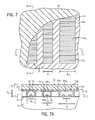
- FIG. 7is a top plan view of the substrate shown in FIG. 6 at a subsequent stage, showing a cutaway of the preferential wetting material over the surface of the self-assembled block copolymer material within the trenches.
- FIGS. 7A and 7Billustrate cross-sectional views of the substrate depicted in FIG. 7 , taken along lines 7 A- 7 A and 7 B- 7 B, respectively.
- FIG. 7Cis a top plan view of a cross-section of the substrate shown in FIG. 7A taken along lines 7 C- 7 C, showing the self-assembled half-cylinder lines within a polymer matrix within the trenches.
- FIG. 8is a view of the substrate depicted in FIG. 7B at a subsequent stage showing removal of the preferential wetting material from the surface of the self-assembled block copolymer material according to an embodiment of the disclosure.
- FIG. 9is a top plan view of the substrate shown in FIG. 7 at a subsequent stage, showing the removal of one of the polymer domains of the self-assembled block copolymer material within the trenches.
- FIGS. 9A and 9Billustrate cross-sectional views of the substrate depicted in FIG. 9 , taken along lines 9 A- 9 A and 9 B- 9 B, respectively.
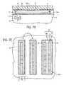
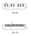
- FIGS. 10 and 11are top plan views of the substrate of FIG. 9 at subsequent stages, illustrating an embodiment of the use of the self-assembled block copolymer film after removal of one of the polymer blocks, as a mask to etch the substrate and filling of the etched openings.
- FIGS. 10A and 11Aillustrate elevational, cross-sectional views of a portion of the substrate depicted in FIGS. 10 and 11 taken along lines 10 A- 10 A and 11 A- 11 A, respectively.
- FIGS. 10B and 11Bare cross-sectional views of the substrate depicted in FIGS. 10 and 11 taken along lines 10 B- 10 B and 11 B- 11 B, respectively.
- FIG. 12is a view of the substrate depicted in FIG. 5A at a subsequent stage showing application of a preferential wetting atmosphere over the block copolymer material within the trenches according to another embodiment of the invention.
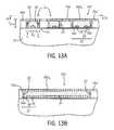
- FIG. 13is a top plan view of the substrate shown in FIG. 12 at a subsequent stage, showing a preferential wetting brush layer over the surface of the self-assembled block copolymer material within the trenches.
- FIGS. 13A and 13Billustrate cross-sectional views of the substrate depicted in FIG. 13 , taken along lines 13 A- 13 A and 13 B- 13 B, respectively.
- semiconductor substratesemiconductor substrate
- semiconductor wafer fragmentsemiconductor wafer fragment
- wafer fragmentwafer fragment
- waferwafer fragment
- waferwafer
- semiconductor materialincluding, but not limited to, bulk semiconductive materials such as a semiconductor wafer (either alone or in assemblies comprising other materials thereon), and semiconductive material layers (either alone or in assemblies comprising other materials).
- substraterefers to any supporting structure including, but not limited to, the semiconductive substrates, wafer fragments or wafers described above.
- L ois the inherent periodicity or pitch value (bulk period or repeat unit) of structures that self-assemble upon annealing from a self-assembling (SA) block copolymer.
- L Bis the periodicity or pitch value of a blend of a block copolymer with one or more of its constituent homopolymers.
- Lis used herein to indicate the center-to-center cylinder pitch or spacing of cylinders of the block copolymer or blend, and is equivalent to “L o ” for a pure block copolymer and “L B ” for a copolymer blend.
- a polymer materiale.g., film, layer
- a polymer materialis prepared by guided self-assembly of block copolymers, with both polymer domains wetting the interface with the trench floor.
- Block copolymer materialsspontaneously assemble into periodic structures by microphase separation of the constituent polymer blocks after annealing, forming ordered domains at nanometer-scale dimensions.
- one or more rows or lines of parallel-oriented half-cylindersare formed within a trench, with the face of the half-cylinder lines wetting a chemically neutral trench floor.
- the parallel-oriented line(s) formed on the substratecan then be used, for example, as an etch mask for patterning nanometer-scale line openings into the underlying substrate through selective removal of one block of the self-assembled block copolymer.
- MWchain length of a block copolymer
- resolutioncan exceed other techniques such as conventional photolithography. Processing costs using the technique are significantly less than extreme ultraviolet (EUV) photolithography, which has comparable resolution.
- EUVextreme ultraviolet
- FIGS. 1-9A method for fabricating a self-assembled block copolymer material that defines an array of nanometer-scale, parallel-oriented, downward facing half-cylinder lines according to an embodiment of the invention is illustrated in FIGS. 1-9 .
- the described embodimentinvolves an anneal of a cylindrical-phase block copolymer in combination with a graphoepitaxy technique that utilizes a lithographically defined trench as a guide with a floor composed of a material that is neutral wetting to both polymer blocks and sidewalls and ends that are preferential wetting to one polymer block and function as constraints to induce self-assembly of the block copolymer material.
- a lithographically defined trench as a guide with a floorcomposed of a material that is neutral wetting to both polymer blocks and sidewalls and ends that are preferential wetting to one polymer block and function as constraints to induce self-assembly of the block copolymer material.
- an overlying material layer that is preferential wettingis placed over the block copolymer material in the trench.
- an air interfacecan selectively wet the desired block.
- the block copolymer materialUpon annealing, the block copolymer material will self-assemble into one or more rows or lines of half-cylinders in a polymer matrix and registered to the trench sidewalls, with the face of the half-cylinders oriented downward and wetting the trench floor.
- an ordered array of two or more rows of half-cylinderscan be formed in each trench.
- a substrate 10which can be silicon, silicon oxide, silicon nitride, silicon oxynitride, silicon oxycarbide, among other materials.
- a neutral wetting material 12(e.g., random copolymer, blend of functionalized homopolymers, etc.) has been formed over the substrate 10 .
- a material layer 14(or one or more material layers) can then be formed over the neutral wetting material and etched to form trenches 16 , 16 a , as shown in FIGS. 2-2B . Portions of the material layer 14 form a spacer 18 outside and between the trenches 16 , 16 a .
- the trenches 16 , 16 aare structured with opposing sidewalls 20 , opposing ends 22 , a floor 24 , a width (w t , w t2 ), a length (l t ) and a depth (D t ).
- the material layer 14 ′can be formed on the substrate 10 ′, etched to form the trenches 16 ′, 16 a ′, and a neutral wetting material 12 ′ can then be formed on the trench floors 24 ′.
- a random copolymer materialcan be deposited into the trenches 16 ′, 16 a ′ and crosslinked or grafted to form a neutral wetting material layer. Material on surfaces outside the trenches 16 ′, 16 a ′, such as on spacers 18 ′ (e.g., non-crosslinked random copolymer) can be subsequently removed.
- Single or multiple trenches 16 , 16 acan be formed using a lithographic tool having an exposure system capable of patterning at the scale of L (10 to 100 nm).
- exposure systemsinclude, for example, extreme ultraviolet (EUV) lithography, proximity X-rays and electron beam (e-beam) lithography, as known and used in the art.
- EUVextreme ultraviolet
- e-beamelectron beam
- Conventional photolithographycan attain (at smallest) about 58 nm features.
- a method called “pitch doubling” or “pitch multiplication”can also be used for extending the capabilities of photolithographic techniques beyond their minimum pitch, as described, for example, in U.S. Pat. No. 5,328,810 (Lowrey et al.), U.S. Pat. No. 7,115,525 (Abatchev et al.), U.S. Patent Publication No. 2006/0281266 (Wells) and U.S. Patent Publication No. 2007/0023805 (Wells).
- a pattern of linesis photolithographically formed in a photoresist material overlying a layer of an expendable material, which in turn overlies a substrate, the expendable material layer is etched to form placeholders or mandrels, the photoresist is stripped, spacers are formed on the sides of the mandrels, and the mandrels are then removed leaving behind the spacers as a mask for patterning the substrate.
- the initial photolithographyformed a pattern defining one feature and one space
- the same widthnow defines two features and two spaces, with the spaces defined by the spacers.
- the smallest feature size possible with a photolithographic techniqueis effectively decreased down to about 30 nm or less.
- Factors in forming a single line or multiple lines of parallel-oriented half-cylinders within the trenchesinclude the width (w t ) of the trench, the formulation of the block copolymer or blend to achieve the desired pitch (L), and the thickness (t) of the block copolymer material.
- trenches 16are constructed with a width (w t ) of about 1.5 to 2 times L (or 1.5-2 ⁇ the pitch value) of the block copolymer material 26 such that a cast block copolymer material (or blend) of about L will self-assemble upon annealing into a single parallel-oriented, downward-facing half-cylinder line (line width at or about 0.5 times L) that is aligned with the sidewalls 20 down the center of each trench 16 .
- a relatively wider trench 16 ahas been formed with a width (w t2 ) of (n+1)*L such that the block copolymer material 26 (or blend) of about L will self-assemble into n lines of downward-facing half-cylinders (line width ⁇ about 0.5 times L) at a center-to-center pitch distance (p) of adjacent lines at or about the L value of the block copolymer material 26 .
- the width (w t2 ) of a wider trench 16 acan be about 3 to 65 times L to result in the formation of 2 to 64 rows, respectively, of the downward-facing half-cylinders.
- the block copolymer materialin trenches 16 with a width (w t ) of about 1.5 to 2 times 50 nm or about 75 nm to 100 nm, the block copolymer material will form a single downward-facing half-cylinder having a line width of about 25 nm.
- the block copolymer materialIn trench 16 a with a width (w t2 ), for example, of about 3 times L or about 3 times 50 nm (or about 150 nm), the block copolymer material will form two rows of the half-cylinder structures (line width of about 2 5nm) at a center-to-center pitch distance (p) of adjacent half-cylinder lines of about the L value (about 50 nm).
- a single line of about 17.5 nm wide (about 0.5 times L) of a downward facing half-cylinderwill form in trench 16 having a width (w t ) of about 1.5 to 2 times L or about 52.5 nm to 70 nm wide, and two parallel lines of half-cylinders (each about 17.5 nm wide) at a center-to-center pitch distance (p) of about 35 nm will form in trench 16 a having a width (w 12 ) of about 3 times L or about 3 times 35 nm (or about 105 nm).
- the length (l t ) of the trenches 16 , 16 ais according to the desired length of the half-cylinder line(s).
- the depth (D t ) of the trenches 16 , 16 ais effective to direct lateral ordering of the block copolymer material during the anneal.
- the trench depthcan be at or less than the final thickness (t 2 ) of the block copolymer material (D t ⁇ t 2 ), which minimizes the formation of a meniscus and variability in the thickness of the block copolymer material across the trench width.
- the trench depthis at about two-thirds (2 ⁇ 3) to about three-fourths (3 ⁇ 4), or about 67% to 75% less than the final thickness (t 2 ) of the block copolymer material within the trench.
- the dimensions of the trenches 16 , 16 aare a width of about 20 nm to 100 nm (trench 16 , w t ) and about 20 nm to 3200 nm (trench 16 a , w t2 ), a length (l t ) of about 100 ⁇ m to 25,000 ⁇ m, and a depth (D t ) of about 10 nm to 100 nm.
- a self-assembling, cylindrical-phase block copolymer material 26 having an inherent pitch at or about L o(or a ternary blend of block copolymer and homopolymers blended to have a pitch at or about L B ) is deposited into the trenches 16 , 16 a .
- a thin layer or film 26 a of the block copolymer material 26can be deposited onto the material layer 14 outside the trenches 16 , 16 a , e.g., on the spacers 18 .
- the block copolymer material 26 or blendis constructed such that all of the polymer blocks will have equal preference for a neutral wetting material on the trench floor 24 .
- the block copolymer or blendis constructed such that the major domain can be selectively removed.
- the minor domain polymer blockcan be selectively doped or structured to incorporate an inorganic component or species (e.g., a filler component) during annealing into microphase domains, which will remain on the substrate 10 as an etch resistant material (e.g., mask) upon selective removal of the majority polymer domain or, in some embodiments, both the majority and minority polymer domains.
- Suitable inorganic precursorsare thermally stable and do not volatilize at the anneal temperature.
- Block copolymers that incorporate an inorganic speciescan be prepared by techniques known in the art, for example, by a direct synthesis technique, or by incorporating atoms of an inorganic species by complexation or coordination with a reactive group of one of the polymer blocks.
- the block copolymercan be blended with an inorganic heat resistant material or precursor thereof, which will segregate to one polymer phase, for example, a metal salt, a metal oxide gel, metal alkoxide polymers, metal oxide precursor, metal nitride precursor, and metal fine particles.
- a metal saltfor example, silicon (Si), chromium (Cr), titanium (Ti), aluminum (Al), molybdenum (Mo), gold (Au), platinum (Pt), ruthenium (Ru), zirconium (Zr), tungsten (W), vanadium (V), lead (Pb), and zinc (Zn), among others.
- metal alkoxidesexamples include alkoxysilanes such as tetramethoxysilane, tetraethoxysilane, tetraisopropoxysilane, tetraisopropoxyaluminum and tetraisopropoxytitanium, and alkylalkoxysilanes such as butyltriethoxysilane and propyltriethoxyaluminum.
- alkoxysilanessuch as tetramethoxysilane, tetraethoxysilane, tetraisopropoxysilane, tetraisopropoxyaluminum and tetraisopropoxytitanium
- alkylalkoxysilanessuch as butyltriethoxysilane and propyltriethoxyaluminum.
- An example of the metal alkoxide polymeris polydiethoxysiloxane.
- metal oxide precursor or metal nitride precursorexamples include polysilsesquioxane (e.g., polymethylsilsesquioxane, polymethylhydroxyl silsesquioxane, polyphenylsilsesquioxane, etc.), polyhedral oligomeric silsesquioxane (POSS), and polysilazane.
- polysilsesquioxanee.g., polymethylsilsesquioxane, polymethylhydroxyl silsesquioxane, polyphenylsilsesquioxane, etc.
- PESpolyhedral oligomeric silsesquioxane
- polysilazaneexamples include polysilsesquioxane (e.g., polymethylsilsesquioxane, polymethylhydroxyl silsesquioxane, polyphenylsilsesquioxane, etc.), polyhedral oligomeric silsesquioxane (
- a solution of a block copolymercan be combined with an additive such as an organic metal salt that has a high affinity to one of the polymer chains of the block copolymer and will segregate during an anneal to one of the polymer phases.
- an additivesuch as an organic metal salt that has a high affinity to one of the polymer chains of the block copolymer and will segregate during an anneal to one of the polymer phases.
- the block copolymercan be mixed with a metal salt combined with an organic compound.
- organic metal saltsexamples include lithium 2,4-pentanedionate, lithium tetramethylpentanedionate, ruthenium 2,4-pentanedionate, magnesium 2,4-pentanedionate, magnesium hexafluoropentanedionate, magnesium trifluoropentanedionate, manganese(II) 2,4-pentanedionate, molybdenum(V) ethoxide, molybdenum(VI) oxide bis(2,4-pentanedionate), neodymium 6,6,7,7,8,8,8-heptafluoro-2,2-dimethyl-3,5-octanedionate, neodymium hexafluoropentanedionate, neodymium(III) 2,4-pentanedionate, nickel(II) 2,4-pentanedionate, niobium(V) n-butoxide,
- atoms of an inorganic speciessuch as a metal (e.g., iron, cobalt, molybdenum, etc.) can be incorporated into one block of a diblock copolymer by complexation of the atoms of the inorganic species with the pyridine units of poly(styrene)-b-poly(vinylpyridine) (PS-b-PVP), where the pyridine group forms a coordination bond with the inorganic species, e.g., iron (Fe), etc., or forms as an acid-base conjugate.
- a metale.g., iron, cobalt, molybdenum, etc.
- PS-b-PVPpoly(styrene)-b-poly(vinylpyridine)
- the pyridine groupforms a coordination bond with the inorganic species, e.g., iron (Fe), etc., or forms as an acid-base conjugate.
- a solution of the PS-b-PVP block copolymercan be combined with dihydrogen hexachloroplatinate (H 2 PtCl 6 ) wherein a single Pt atom can be complexed with each pyridine group (at maximum loading).
- H 2 PtCl 6dihydrogen hexachloroplatinate
- block copolymers that incorporate an inorganic speciescan also be prepared by a direct synthesis technique.
- a sequential living polymerization of a nonmetal-containing monomere.g., styrene monomer
- an inorganic species-containing monomere.g., ferrocenylethylmethylsilane monomer
- PS-b-PFEMSpoly(styrene)-b-poly(ferrocenylmethylethylsilane)
- diblock copolymersinclude, for example, poly(styrene)-b-poly(vinylpyridine) (PS-b-PVP), poly(styrene)-b-poly(methylmethacrylate) (PS-b-PMMA) or other PS-b-poly(acrylate) or PS-b-poly(methacrylate), poly(styrene)-b-poly(lactide) (PS-b-PLA), poly(styrene)-b-poly(tert-butyl acrylate) (PS-b-PtBA), and poly(styrene)-b-poly(ethylene-co-butylene (PS-b-(PS-co-PB)), and poly(styrene)-b-poly(ethylene oxide) (PS-b-PEO), polybutadiene-b-poly(vinylpyridine) (PB-b-PVP), poly(ethylene-alt-propylene)-b-poly(ethylene
- block copolymersi.e., triblock or multiblock copolymers
- triblock copolymersinclude ABC copolymers such as poly(styrene-b-methylmethacrylate-b-ethylene oxide) (PS-b-PMMA-b-PEO), and ABA copolymers such as PS-PMMA-PS, PMMA-PS-PMMA, and PS-b-PI-b-PS, among others.
- an oxidation processe.g., ultraviolet (UV)-ozonation or oxygen plasma etching
- UV-ozonation or oxygen plasma etchingcan be performed to remove the organic components of the block copolymer domains and convert the inorganic species to form a non-volatile inorganic oxide, which remains on the substrate and can be used as a mask in a subsequent etch process.
- the inorganic species of the PDMS and PFEM block copolymersare silicon and iron, which, upon oxidation, will form non-volatile oxides, e.g., silicon oxide (SiO x ) and iron oxide (Fe x O y ).
- the L value of the block copolymercan be modified, for example, by adjusting the molecular weight of the block copolymer.
- the block copolymer materialcan also be formulated as a binary or ternary blend comprising a block copolymer and one or more homopolymers (HPs) of the same type of polymers as the polymer blocks in the block copolymer, to produce a blend that will swell the size of the polymer domains and increase the L value.
- the concentration of homopolymers in a blendcan range from 0 wt% to about 60 wt%. Generally, when added to a polymer material, both homopolymers are added to the blend in about the same ratio or amount.
- a ternary diblock copolymer blendis a PS-b-PVP/PS/PVP blend, for example, 60 wt% of 32.5 K/12 K PS-b-PVP, 20 wt% of 10K PS, and 20 wt% of 10K PVP.
- Another example of a ternary diblock copolymer blendis a PS-b-PMMA/PS/PMMA blend, for example, 60 wt% of 46K/21K PS-b-PMMA, 20 wt% of 20K polystyrene and 20 wt% of 20K poly(methylmethacrylate).
- Yet another exampleis a blend of 60:20:20 (wt%) of PS-b-PEO/PS/PEO, or a blend of about 85 to 90 wt% PS-b-PEO and up to 10 to 15 wt% PEO homopolymer.
- the film morphologyincluding the domain sizes and periods (L o ) of the microphase-separated domains, can be controlled by chain length of a block copolymer (molecular weight, MW) and volume fraction of the AB blocks of a diblock copolymer to produce cylindrical morphologies (among others).
- a block copolymermolecular weight, MW
- volume fraction of the AB blocks of a diblock copolymerto produce cylindrical morphologies (among others).
- the diblock copolymerwill microphase separate and self-assemble into periodic half-cylindrical domains of polymer B within a matrix of polymer A.
- An example of a cylinder-forming PS-b-PVP copolymer material (L o ⁇ 35 nm) to form about 20 nm wide half-cylindrical PVP domains in a matrix of PSis composed of about 70 wt% PS and 30 wt% PVP with a total molecular weight (M n ) of 44.5 kg/mol.
- the cylindrical-phase block copolymer material 26can be cast or deposited into the trenches 16 , 16 a to an initial thickness (t 1 ) at or about the L value of the block copolymer material 26 (e.g., about ⁇ 20% of L) such that the thickness (t 2 ) after annealing will be at or below the L value and the block copolymer material 26 will self-assemble to form a single layer of downwardly facing half-cylinders registered parallel to the sidewalls 20 and extending the length (l t ) of each of the trenches 16 , 16 a (e.g., as in FIGS. 7A and 7B ).
- the thickness of the block copolymer material 26can be measured, for example, by ellipsometry techniques.
- the block copolymer material 26can be deposited by spin-casting (spin-coating) from a dilute solution (e.g., about 0.25 wt% to 2 wt % solution) of the copolymer in an organic solvent such as dichloroethane (CH 2 Cl 2 ) or toluene, for example. Capillary forces pull excess block copolymer material 26 (e.g., greater than a monolayer) into the trenches 16 , 16 a . As shown, a thin layer or film 26 a of the block copolymer material 26 can be deposited onto the material layer 14 outside the trenches 16 , 16 a , e.g., on the spacers 18 . Upon annealing, the thin film 26 a will flow into the trenches 16 , 16 a leaving a structureless brush layer on the material layer 14 from a top-down perspective.
- a dilute solutione.g., about 0.25 wt% to 2 wt
- the trench floors 24are structured to be neutral wetting (equal affinity for both blocks of the copolymer) to induce formation of half-cylinder polymer domains that are oriented facing downward on the trench floors 24
- the trench sidewalls 20 and the ends 22are structured to be preferential wetting by one block of the block copolymer to induce registration of the half-cylinders to the sidewalls 20 as the polymer blocks self-assemble.
- Entropic forcesdrive the wetting of a neutral wetting surface by both blocks
- enthalpic forcesdrive the wetting of a preferential-wetting surface by the preferred block (e.g., the minority block).
- a chemically neutral wetting trench floor 24allows both blocks of the copolymer material to wet the floor 24 of the trenches 16 , 16 a and provides for the formation of the half-cylinder line layout of the disclosure.
- the use of a neutral wetting trench floor in embodiments of the inventionexpands the number of block copolymer materials that can be utilized to produce self-assembled films having a series of parallel lines formed on a substrate surface that can be readily used as a mask for etching the underlying substrate to form a multiple line layout on a nanoscale level.
- a neutral wetting material 12can be provided, for example, by applying a neutral wetting polymer (e.g., a neutral wetting random copolymer) onto the substrate 10 , then forming an overlying material layer 14 and etching the trenches 16 , 16 a to expose the underlying neutral wetting material, as illustrated in FIGS. 2-2B .
- a neutral wetting polymere.g., a neutral wetting random copolymer
- a neutral wetting random copolymer materialcan be applied after forming the trenches 16 ′, 16 a ′, for example, as a blanket coat by casting or spin-coating into the trenches 16 ′, 16 a ′ as depicted in FIG. 4 .
- the random copolymer materialcan then be thermally processed to flow the material into the bottom of the trenches 16 ′, 16 a ′ by capillary action, which results in a layer (mat) 12 ′ composed of the crosslinked, neutral wetting random copolymer.
- the random copolymer material within the trenches 16 ′, 16 a ′can be photo-exposed (e.g., through a mask or reticle) to crosslink the random copolymer within the trenches 16 ′, 16 a ′ to form the neutral wetting material 12 ′.
- Non-crosslinked random copolymer material outside the trenches 16 ′, 16 a ′e.g., on the spacers 18 ′
- Neutral wetting surfacescan be specifically prepared by the application of random copolymers composed of monomers identical to those in the block copolymer and tailored such that the mole fraction of each monomer is appropriate to form a neutral wetting surface.
- a neutral wetting material 12can be formed from a thin film of a photo-crosslinkable random PS-r-PVP copolymer that exhibits non-preferential or neutral wetting toward PS and PVP, which can be cast onto the substrate 10 (e.g., by spin coating).
- the random copolymer materialcan be fixed in place by chemical grafting (on an oxide substrate) or by thermally or photolytically crosslinking (any surface) to form a mat that is neutral wetting to PS and PVP and insoluble when the block copolymer material is cast onto it, due to the crosslinking.
- a blend of hydroxyl-terminated homopolymers and a corresponding low molecular weight block copolymercan be grafted (covalently bonded) to the substrate to form a neutral wetting interface layer (e.g., about 4 nm to 5 nm) for PS-b-PMMA and PS-b-P2VP, among other block copolymers.
- the block copolymercan function to emulsify the homopolymer blend before grafting.
- an about 1 wt% solutione.g., in toluene
- a substrate 10e.g., SiO 2
- heated (baked)e.g., at 160° C.
- the non-grafted (unbonded) polymer materialmay be removed, for example, by a solvent rinse (e.g., toluene).
- a neutral wetting surface for PS-b-PMMAcan be provided by hydrogen-terminated silicon.
- the floors 24 of the trenches 16 , 16 acan be etched, for example, with a hydrogen plasma, to remove the oxide material and form hydrogen-terminated silicon, which is neutral wetting with equal affinity for both blocks of a block copolymer material.
- H-terminated siliconcan be prepared by a conventional process, for example, by a fluoride ion etch of a silicon substrate (with native oxide present, about 12 ⁇ to 15 ⁇ ) by exposure to an aqueous solution of hydrogen fluoride (HF) and buffered HF or ammonium fluoride (NH 4 F), by HF vapor treatment, or by a hydrogen plasma treatment (e.g., atomic hydrogen).
- a fluoride ion etch of a silicon substratewith native oxide present, about 12 ⁇ to 15 ⁇
- HFhydrogen fluoride
- NH 4 Fbuffered HF or ammonium fluoride
- HF vapor treatmente.g., atomic hydrogen
- An H-terminated silicon substratecan be further processed by grafting a random copolymer such as PS-r-PVP, PS-r-PMMA, etc., selectively onto the substrate 10 , resulting in a neutral wetting surface for the corresponding block copolymer (e.g., PS-b-PVP, PS-b-PMMA, etc.).
- a neutral wetting layer of a PS-r-PMMA random copolymercan be provided by an in situ free radical polymerization of styrene and methylmethacrylate using a di-olefinic linker such as divinyl benzene, which links the copolymer to an H-terminated silicon surface to produce about a 10-nm to 15-nm thick film.
- a neutral wetting random copolymer material 12 ′can be applied after formation of the material layer 14 ′ and trenches 16 ′, 16 a ′, which reacts selectively with the trench floor 24 ′ (composed of the substrate 10 ′ material) and not the trench sidewalls 20 ′ or ends 22 ′ (composed of the material layer 14 ′).
- a random copolymer (or appropriate blend of homopolymers with a block copolymer surfactant) containing epoxide groupswill react selectively to terminal amine functional groups (e.g., —NH— and —NH 2 ) on silicon nitride and silicon oxynitride surfaces relative to silicon oxide or silicon.
- terminal amine functional groupse.g., —NH— and —NH 2
- the trench floor 24 ′is silicon or polysilicon and the sidewalls 20 ′ are a material such as an oxide (e.g., SiO x ), the floor 24 ′ can be treated to form H-terminated silicon and a random copolymer material (e.g., PS-r-PVP, PS-r-PMMA, etc.) can be formed by in situ polymerization only at the floor surface.
- a random copolymer materiale.g., PS-r-PVP, PS-r-PMMA, etc.
- a neutral wetting surface(e.g., for PS-b-PMMA and PS-b-PEO) can be provided by grafting a self-assembled monolayer (SAM) of a trichlorosilane-base SAM such as 3-(para-methoxyphenyl)propyltrichorosilane grafted to oxide (e.g., SiO 2 ) as described, for example, by D. H. Park, Nanotechnology 18 (2007), p. 355304.
- SAMself-assembled monolayer
- oxidee.g., SiO 2
- a surface that is neutral wetting to PS-b-PMMAcan also be prepared by spin-coating a blanket layer of a photo- or thermally crosslinkable random copolymer such as a benzocyclobutene- or azidomethylstyrene-functionalized random copolymer of styrene and methylmethacrylate (e.g., poly(styrene-r-benzocyclobutene-r-methylmethacrylate (PS-r-PMMA-r-BCB)).
- a photo- or thermally crosslinkable random copolymersuch as a benzocyclobutene- or azidomethylstyrene-functionalized random copolymer of styrene and methylmethacrylate (e.g., poly(styrene-r-benzocyclobutene-r-methylmethacrylate (PS-r-PMMA-r-BCB)).
- such a random copolymercan comprise about 42 wt% PMMA, about (58-x) wt% PS and x wt% (e.g., about 2 wt% to 3 wt%) of either polybenzocyclobutene or poly(para-azidomethylstyrene)).
- An azidomethylstyrene-functionalized random copolymercan be UV photo-crosslinked (e.g., 1 MW/cm 2 to 5 MW/cm 2 exposure for about 15 seconds to about 30 minutes) or thermally crosslinked (e.g., at about 170° C. for about four hours) to form a crosslinked polymer mat as a neutral wetting layer.
- a benzocyclobutene-functionalized random copolymercan be thermally crosslinked (e.g., at about 200° C. for about four hours or at about 250° C. for about ten minutes).
- a neutral wetting random copolymer of polystyrene (PS), polymethacrylate (PMMA) with hydroxyl group(s)e.g., 2-hydroxyethyl methacrylate (P(S-r-MMA-r-HEMA)) (e.g., about 58 wt% PS)
- a substrate 10e.g., an oxide
- a neutral wetting layerabout 5 nm to 10 nm thick by heating at about 160° C. for about 48 hours. See, for example, In et al., Langmuir, 2006, 22, 7855-7860.
- the material layer 14can be composed of silicon (with native oxide), oxide (e.g., silicon oxide, SiO x ), silicon nitride, silicon oxycarbide, indium tin oxide (ITO), silicon oxynitride, and resist materials such as methacrylate-based resists and polydimethyl glutarimide resists, among other materials, which exhibit preferential wetting toward the preferred block (e.g., the minority block), which is the PVP block in the illustrated embodiment.
- siliconwith native oxide
- oxidee.g., silicon oxide, SiO x
- silicon nitridesilicon oxycarbide
- ITOindium tin oxide
- resist materialssuch as methacrylate-based resists and polydimethyl glutarimide resists, among other materials, which exhibit preferential wetting toward the preferred block (e.g., the minority block), which is the PVP block in the illustrated embodiment.
- the preferred blocke.g., the PVP block
- the preferred blockwill form a thin interface layer along the preferential wetting sidewalls 20 and ends 22 of the trenches 16 , 16 a.
- a preferential wetting materialsuch as a polymethylmethacrylate (PMMA) polymer modified with an —OH containing moiety (e.g., hydroxyethylmethacrylate) can be selectively applied onto the sidewalls of the trenches in embodiments where a neutral wetting material 12 , 12 ′, is in place on the trench floor 24 , 24 ′ (as in FIGS. 2-2B and FIG. 4 ).
- a neutral wetting layercan be formed on the trench floor 24 , 24 ′ (e.g., depicted in FIG.
- OH-modified PMMAcan be applied, for example, by spin coating and then heating (e.g., to about 170° C.) to allow the terminal OH groups to selectively end-graft to the sidewalls 20 and ends 22 (e.g., of oxide) of the trenches 16 , 16 a , 16 ′, 16 a ′.
- Non-grafted materialcan be removed by rinsing with an appropriate solvent (e.g., toluene). See, for example, Mansky et al., Science, 1997, 275, 1458-1460, and In et al., Langmuir, 2006, 22, 7855-7860.
- a surface 28 of the block copolymer material 26 in the trenches 16 , 16 ais then contacted by a material 30 that will preferentially wet one of the blocks of the copolymer material 26 , which is the minority block in the illustrated embodiment.
- the preferential wetting material 30is composed of a solid material that is placed onto the surface of the block copolymer material 26 .
- the preferential wetting material 30can be composed of a soft, flexible or rubbery solid material such as a crosslinked poly(dimethylsiloxane) (PDMS) elastomer (e.g., Sylgard 184 by Dow Corning Corp., Midland, Mich.) or other elastomeric polymer material (e.g., silicones, polyurethanes, etc.).
- PDMSpoly(dimethylsiloxane)
- a crosslinked, solid PDMS material 30provides an external surface that is hydrophobic, which can be altered, for example, by a plasma oxidation to add silanol (SiOH) groups to the surface to render the PDMS surface hydrophilic.
- a PDMS material 30 having a hydrophobic surface placed into contact with the PS-b-PVP block copolymer material 26will be preferentially wetted by the PS block, while a PDMS material 30 modified with a hydrophilic surface will be preferentially wetted by the PVP block.
- a PDMS material 30can be removed, for example, by lifting or peeling the material 30 from the surface 28 of the block copolymer material 26 , which can include applying a solvent such as water, alcohols, etc. (e.g., by soaking), to permeate and swell the PDMS material 30 to enhance physical removal, and which is compatible with and does not dissolve the block copolymer.
- a dilute fluoride solutione.g., NH 4 F, HF, NaF, etc.
- the preferential wetting material 30can be formed as an inorganic film on the surface 28 of the block copolymer material 26 .
- a layer of a spin-on dielectric (SOD) materialcan be formed by applying, for example, a spin-on liquid silicon-containing polymer, removing the solvent (e.g., by heating), and then oxidizing the polymer layer (e.g., oxygen atmosphere, steam-oxidation process, wet chemical oxidation, etc.) to form a hard silicon dioxide (SiO 2 ) layer, a hydrophilic surface that will be preferentially wetted by the PVP (minority) block.
- SODspin-on dielectric
- the oxidationcan be conducted simultaneously with a thermal anneal of the block copolymer material 26 .
- silicon-containing polymersinclude silicates, siloxanes (e.g., hydrogen silsesquioxane (HSQ), hexamethyldisiloxane, octamethyltrisiloxane, etc.), silazanes (e.g., polysilazanes such as hexamethyldisilazane (HMDS), tetramethyldisilazane, octamethylcyclotetrasilazine, hexamethylcyclotrisilazine, diethylaminotrimethylsilane, dimethylaminotrimethylsilane, etc.) and silisesquioxanes (e.g., hydrogen silsesquioxane (HSQ).
- siloxanese.g., hydrogen silsesquioxane (HSQ)
- HMDShexamethyld
- the spin-on polymer materialcan be applied, for example, by casting, spin applying, flow coating or a spray coating technique.
- the solvent of the spin-on polymer materialis compatible with and does not dissolve the block copolymer, for example, water or an alcohol.
- a layer of dielectric preferential wetting material 30can be removed using a controlled etch back process, for example, by applying a fluoride-based etchant whereby the dielectric material is etched at a low etch rate (e.g., less than about 200 ⁇ /minute).
- an annealing processis conducted (arrows ⁇ , FIG. 6 ) to cause the polymer blocks to phase separate in response to the preferential and neutral wetting of the trench surfaces and the preferential wetting of the overlying material 30 , and form a self-assembled polymer material 32 as illustrated in FIGS. 7-7C .
- Thermal annealingcan be conducted at above the glass transition temperature of the component blocks of the copolymer material 26 (see FIG. 6 ).
- a PS-b-PVP copolymer materialcan be globally annealed at a temperature of about 150° C. to 275° C. in a vacuum oven for about 1 hour to 24 hours to achieve the self-assembled morphology.
- the resulting morphology of the annealed copolymer material 32(e.g., parallel orientation of the half-cylinder lines) can be examined, for example, using atomic force microscopy (AFM), transmission electron microscopy (TEM), scanning electron microscopy (SEM).
- AFMatomic force microscopy
- TEMtransmission electron microscopy
- SEMscanning electron microscopy
- the block copolymer material 26can be globally heated or, in other embodiments, a zone or localized thermal anneal can be applied to portions or sections of the block copolymer material 26 .
- the substrate 10can be moved across a hot-to-cold temperature gradient 34 ( FIG. 6 ) positioned above (as shown) or underneath the substrate 10 (or the thermal source can be moved relative to the substrate 10 , e.g., arrow ⁇ ) such that the block copolymer material 26 self-assembles upon cooling after passing through the heat source. Only those portions of the block copolymer material 26 that are heated above the glass transition temperature of the component polymer blocks will self-assemble, and areas of the material that were not sufficiently heated remain disordered and unassembled. “Pulling” the heated zone across the substrate 10 can result in faster processing and better ordered structures relative to a global thermal anneal.
- the cylindrical-phase block copolymer material 26Upon annealing, the cylindrical-phase block copolymer material 26 will self-assemble into a polymer material 32 (e.g., a film), as depicted in FIGS. 7-7C .
- the cylinder-phase block copolymer compositione.g., 70:30 PS-b-PVP having an inherent pitch at or about L
- the boundary conditionsincluding the constraints provided by the width (w t ) of the trenches 16 and the wetting properties of the trench surfaces (i.e., a trench floor 24 that exhibits neutral or non-preferential wetting toward both polymer blocks, e.g., a random graft copolymer, and trench sidewalls 20 and an overlying material 30 that are preferential wetting to the minority block
- the minority (preferred) blocke.g., PVP
- the minority (preferred) blockwill self-assemble to form parallel-oriented, downward-facing, half-cylinder domain (line) 36 on the non-pre
- a matrix 38 of the majority polymer block(e.g., PS) overlies and surrounds the half-cylinder(s) 36 .
- the lines of the half-cylinder 36(both blocks considered) will have a width (w t ) at or about 0.5 times L.
- the minority (preferred) block(e.g., PVP) will segregate to and wet the preferential wetting sidewalls 20 and ends 22 of the trenches 16 , 16 a to form a thin interface or wetting (brush) layer 36 a , and will segregate to and wet the overlying preferential wetting material layer 30 to form an overlying thin wetting layer 36 a s .
- the thickness of the wetting layers 36 a , 36 a s(both blocks considered) is generally about 0.5 times L, which includes ⁇ 0.25 times L of the minority block and about 0.25 times L of the majority block. For example, a ⁇ 0.25 times L thick layer of the PVP block will wet oxide interfaces with attached PS domains (about 0.25 times L thick) directed outward from the oxide material.
- the block copolymer material 26includes an inorganic species such as a metal (e.g., Si, Fe, etc.)
- the inorganic specieswill segregate to one polymer phase upon annealing.
- a PS-b-PVP copolymercombined with a silicon- and/or iron-containing additive where the pyridine group selectively solvates the Si and Fe species
- the Si and Fe specieswill segregate to the PVP half-cylinders 36 (and wetting layers 36 a ).
- Suitable inorganic precursorsare thermally stable and will not volatilize at the anneal temperature.
- the width (w 1 ) of trenches 16are about 1.5 to 2 times L (or 1.5 to 2 ⁇ the pitch value) of the block copolymer 26 , resulting in the formation of a single half-cylinder down the center of the trench 16 from a block copolymer having a pitch value of about L. As depicted in FIGS.
- the block copolymer materialwithin a wider trench 16 a having a width (w 12 ) of about (n+1)*L (or (n+1) X the pitch value), the block copolymer material will self-assemble to form multiple (n) lines of half-cylinders 36 (shown as two lines) with a center-to-center pitch distance (p) of adjacent lines at or about the pitch distance or L value of the block copolymer material.
- the number (n) of half-cylinder lines 36 within a trenchcan be varied, for example, according to the width of the trench and/or the pitch distance (p) or L value of the block copolymer material.
- the preferential wetting material 30can be removed from contact with the assembled block copolymer material 32 , as shown in FIG. 8 .
- the materialin the use of a solid, elastomeric material 30 such as PDMS, the material can be lifted or peeled from the surface of the block copolymer material 32 .
- a solvent that is compatible with and does not dissolve or etch the assembled polymer domainssuch as water, alcohol, etc. can be applied (e.g., by spraying, soaking the material) to permeate and swell the material and enhance removal without altering or damaging the assembled polymer structure.
- a dilute fluoride solutione.g., NH 4 F, HF, NaF, etc.
- the material 30can be removed by a controlled etch back process, for example, by applying a fluoride-based etchant whereby the dielectric material is etched at a low etch rate (e.g., less than about 200 ⁇ /minute) without altering or damaging the assembled polymer structure.
- a fluoride-based etchantwhereby the dielectric material is etched at a low etch rate (e.g., less than about 200 ⁇ /minute) without altering or damaging the assembled polymer structure.
- an elastomeric material 30is used with a block copolymer material that includes an inorganic species (e.g., Si, Fe, etc.)
- a process that dissolves or etches the polymer components but not the inorganic speciescan be used to selectively remove the organic components of the block copolymer domains, leaving the inorganic species on the substrate to form a mask material.
- an oxygen plasma etchwill remove the carbonaceous major domains, leaving inorganic material (e.g., Si, Fe, etc.) as lines on the substrate surface.
- a block copolymer thin film 26 a outside the trenches(e.g., on spacers 18 ) will not be not thick enough to result in self-assembly.
- the unstructured thin film 26 acan be removed, for example, by an etch technique or a planarization process to provide an about uniformly flat surface.
- the copolymer materialcan be treated to crosslink one of the polymer domains (e.g., the PVP half-cylinders) to fix and enhance the strength of the polymer blocks.
- one of the polymer blockscan be structured to inherently crosslink (e.g., upon exposure to ultraviolet (UV) radiation, including deep ultraviolet (DUV) radiation), or the polymer block can be formulated to contain a crosslinking agent.
- UVultraviolet
- DUVdeep ultraviolet
- the trench regionscan be selectively exposed through a reticle (not shown) to crosslink only the self-assembled polymer material 32 within the trenches 16 , 16 a and a wash can then be applied with an appropriate solvent (e.g., toluene) to remove the non-crosslinked portions of the block copolymer material 26 a , leaving the registered self-assembled polymer material 32 within the trench and exposing the surface of the material layer 14 above/outside the trenches.
- an appropriate solvente.g., toluene
- the annealed polymer material 32can be crosslinked globally, a photoresist material can be applied to pattern and expose the areas of the polymer material 26 a outside the trench regions, and the exposed portions of the polymer material 26 a can be removed, for example by an oxygen (O 2 ) plasma treatment.
- O 2oxygen
- An embodiment of the application of the self-assembled polymer material 30is as an etch mask to form openings in the substrate 10 .
- the assembled polymer material 32can be processed to form a structure that can be used as an etch mask to form openings in the substrate 10 .
- the surface wetting layer 36 a s( FIGS. 7A , 7 C) composed of the minority block (e.g., PVP) can be selectively removed to expose the matrix 38 of the self-assembled polymer material 32 .
- a surface wetting layer 36 a s of PVPcan be removed by an RIE process using an oxygen, fluorocarbon, or argon plasma, for example.
- an oxidation processsuch as a UV-ozonation or oxygen plasma etching, can be performed to remove the organic material (i.e., the polymer domains) and convert the inorganic species to a non-volatile inorganic oxide, e.g., silicon oxide (SiO x ), iron oxide (Fe x O y ), etc., which remains on the substrate and can be used as a mask in a subsequent etch process.
- a non-volatile inorganic oxidee.g., silicon oxide (SiO x ), iron oxide (Fe x O y ), etc.
- the block copolymer material ( 26 )is composed of PS-b-PVP combined (e.g., doped) with an Si- and/or Fe-containing additive, and the Si and/or Fe species are segregated to the PVP half-cylinders 36 and wetting layers 36 a .
- An oxidation process(arrows ⁇ ) can be performed to remove both the PS matrix 38 and PVP polymer component of the half-cylinders 36 (and neutral wetting layer 12 ) and convert the Si and/or Fe species within the half-cylinders to inorganic oxide, e.g., SiO x and/or Fe x O y resulting in non-volatile, inorganic oxide lines 40 on the substrate 10 .
- the matrix domain 38 of the self-assembled polymer material 32can be selectively removed relative to the half-cylinder lines 36 , which can be used as a mask to etch the exposed substrate 10 at the trench floor 24 .
- PMMA domainscan be selectively removed by UV exposure/acetic acid development or by selective reactive ion etching (RIE), and the remaining PS domains can then be used as a mask to etch the substrate 10 .
- RIEreactive ion etching
- the oxide lines 40can then be used as a mask to etch line openings 42 (e.g., trenches) in the substrate 10 , as depicted in FIGS. 10 and 10B , for example, using an anisotropic, selective reactive ion etch (RIE) process.
- RIEselective reactive ion etch
- the residual oxide lines 40can be removed, for example, using a fluoride-based etchant, and the substrate openings 42 can be filled with a material 44 such as a metal or metal alloy such as Cu, Al, W, Si, and Ti 3 N 4 , among others, to form arrays of conductive lines, or with an insulating material such as SiO 2 , Al 2 O 3 , HfO 2 , ZrO 2 , SrTiO 3 , and the like.
- a material 44such as a metal or metal alloy such as Cu, Al, W, Si, and Ti 3 N 4 , among others, to form arrays of conductive lines, or with an insulating material such as SiO 2 , Al 2 O 3 , HfO 2 , ZrO 2 , SrTiO 3 , and the like.
- an atmosphere 46 ′can be applied to form an air interface at the surface 28 ′ of the block copolymer material 26 ′ in the trenches that is preferentially wetting to one of the blocks of the copolymer material 26 ′.
- a preferentially wetting atmospherecan be composed of clean, dry air to preferentially wet the polymer block having the lower surface tension.
- the PS blockhas a relatively lower surface tension and will preferentially wet a clean dry air atmosphere.
- the PDMS blockhas a lower surface tension and will preferentially wet a clean dry air atmosphere.
- a humid atmospherecan be applied to preferentially wet PEO over PS (e.g., using PS-b-PEO), or a near-saturated solvent atmosphere (e.g., ethanol, dimethylformamide (DMF), and the like) can be applied as a vapor phase to preferentially wet PVP over the PS block (e.g., using PS-b-PVP).
- a near-saturated solvent atmospheree.g., ethanol, dimethylformamide (DMF), and the like
- DMFdimethylformamide
- An anneal of the block copolymer material 26 ′ in the presence of the preferentially wetting atmosphere 46 ′can then be conducted such that the polymer blocks phase separate in response to the preferential and neutral wetting of the trench surfaces and the preferential wetting of the overlying atmosphere 46 ′ at the air-interface to form a self-assembled polymer material 32 ′ as illustrated in FIGS. 13-13B .
- a cylinder-phase block copolymer compositione.g., 70:30 PS-b-PVP (inherent pitch ⁇ L) will self-assemble such that the minority (preferred) block (e.g., PVP) will form parallel-oriented, downward-facing, half-cylinder domains 36 ′ on the neutral wetting material 12 ′ on the trench floors surrounded by an overlying matrix 38 ′ of the majority polymer block (e.g., PS).
- the minority (preferred) blocke.g., PVP
- PVPminority (preferred) block
- the air interfacee.g., using a near-saturated solvent atmosphere
- the minority blockwill segregate to and wet the sidewalls 20 ′ and ends 22 ′ of the trenches 16 ′, 16 a ′ and the air interface (e.g., using a near-saturated solvent atmosphere), which are preferential wetting to the minority block, to form an thin interface or wetting layer 36 a ′ (on the sidewalls) and 36 a s ′ (at the air interface) (e.g., at a thickness of about 0.25 times L).
- PDMS half-cylinders 26 ′would assemble on the neutral wetting material 12 ′ within an overlying PS matrix 38 ′, and PDMS would form a brush layer 26 a ′ on the trench sidewalls 20 ′ and ends 22 ′ and a brush layer 26 a s ′ at the interface with a clean, dry air atmosphere that would preferentially wet PDMS.
- the polymer material 32 ′can be optionally crosslinked as previously described.
- the surface wetting layer 36 a′ s at the air interfacee.g., the minority block, PVP
- the surface wetting layer 36 a′ s at the air interfacecan be selectively removed to expose the underlying matrix 38 ′, e.g., by an RIE process.
- the self-assembled polymer materialcan then be processed as desired, for example, to form a masking material to etch the underlying substrate 10 ′.
- Embodiments of the inventionprovide methods of forming structures of parallel lines that assemble via graphoepitaxy rapidly and defect-free over large areas in wide trenches.
- the structures formed from cylinder-forming block copolymerscan be produced considerably faster than for lamellar-forming block copolymers, and have improved pattern transfer to an underlying substrate when used as an etch mask compared to arrays of minority block cylinders fully suspended in a majority block matrix due to undercutting of the matrix underneath the cylinders during etching.
- the methodsalso provide ordered and registered elements on a nanometer scale that can be prepared more inexpensively than by electron beam lithography, EUV photolithography or conventional photolithography.
- the feature sizes produced and accessible by this inventioncannot be easily prepared by conventional photolithography.
- the described methods and systemscan be readily employed and incorporated into existing semiconductor manufacturing process flows and provide a low cost, high-throughput technique for fabricating small structures.
Landscapes
- Engineering & Computer Science (AREA)
- Chemical & Material Sciences (AREA)
- Manufacturing & Machinery (AREA)
- Nanotechnology (AREA)
- Physics & Mathematics (AREA)
- General Physics & Mathematics (AREA)
- Condensed Matter Physics & Semiconductors (AREA)
- Microelectronics & Electronic Packaging (AREA)
- Computer Hardware Design (AREA)
- Power Engineering (AREA)
- Materials Engineering (AREA)
- Crystallography & Structural Chemistry (AREA)
- Composite Materials (AREA)
- Analytical Chemistry (AREA)
- Exposure Of Semiconductors, Excluding Electron Or Ion Beam Exposure (AREA)
- Formation Of Insulating Films (AREA)
- Graft Or Block Polymers (AREA)
- Internal Circuitry In Semiconductor Integrated Circuit Devices (AREA)
- Treatments Of Macromolecular Shaped Articles (AREA)
- Laminated Bodies (AREA)
- Catalysts (AREA)
- Micromachines (AREA)
- Element Separation (AREA)
Abstract
Description
Claims (19)
Priority Applications (3)
| Application Number | Priority Date | Filing Date | Title |
|---|---|---|---|
| US13/396,039US8518275B2 (en) | 2008-05-02 | 2012-02-14 | Graphoepitaxial self-assembly of arrays of downward facing half-cylinders |
| US13/928,746US8993088B2 (en) | 2008-05-02 | 2013-06-27 | Polymeric materials in self-assembled arrays and semiconductor structures comprising polymeric materials |
| US14/605,276US20150137331A1 (en) | 2008-05-02 | 2015-01-26 | Polymeric materials in self-assembled arrays and semiconductor structures and methods comprising such polymeric materials |
Applications Claiming Priority (2)
| Application Number | Priority Date | Filing Date | Title |
|---|---|---|---|
| US12/114,173US8114301B2 (en) | 2008-05-02 | 2008-05-02 | Graphoepitaxial self-assembly of arrays of downward facing half-cylinders |
| US13/396,039US8518275B2 (en) | 2008-05-02 | 2012-02-14 | Graphoepitaxial self-assembly of arrays of downward facing half-cylinders |
Related Parent Applications (1)
| Application Number | Title | Priority Date | Filing Date |
|---|---|---|---|
| US12/114,173DivisionUS8114301B2 (en) | 2008-05-02 | 2008-05-02 | Graphoepitaxial self-assembly of arrays of downward facing half-cylinders |
Related Child Applications (1)
| Application Number | Title | Priority Date | Filing Date |
|---|---|---|---|
| US13/928,746DivisionUS8993088B2 (en) | 2008-05-02 | 2013-06-27 | Polymeric materials in self-assembled arrays and semiconductor structures comprising polymeric materials |
Publications (2)
| Publication Number | Publication Date |
|---|---|
| US20120138570A1 US20120138570A1 (en) | 2012-06-07 |
| US8518275B2true US8518275B2 (en) | 2013-08-27 |
Family
ID=41255682
Family Applications (4)
| Application Number | Title | Priority Date | Filing Date |
|---|---|---|---|
| US12/114,173Active2029-02-24US8114301B2 (en) | 2008-05-02 | 2008-05-02 | Graphoepitaxial self-assembly of arrays of downward facing half-cylinders |
| US13/396,039ActiveUS8518275B2 (en) | 2008-05-02 | 2012-02-14 | Graphoepitaxial self-assembly of arrays of downward facing half-cylinders |
| US13/928,746ActiveUS8993088B2 (en) | 2008-05-02 | 2013-06-27 | Polymeric materials in self-assembled arrays and semiconductor structures comprising polymeric materials |
| US14/605,276AbandonedUS20150137331A1 (en) | 2008-05-02 | 2015-01-26 | Polymeric materials in self-assembled arrays and semiconductor structures and methods comprising such polymeric materials |
Family Applications Before (1)
| Application Number | Title | Priority Date | Filing Date |
|---|---|---|---|
| US12/114,173Active2029-02-24US8114301B2 (en) | 2008-05-02 | 2008-05-02 | Graphoepitaxial self-assembly of arrays of downward facing half-cylinders |
Family Applications After (2)
| Application Number | Title | Priority Date | Filing Date |
|---|---|---|---|
| US13/928,746ActiveUS8993088B2 (en) | 2008-05-02 | 2013-06-27 | Polymeric materials in self-assembled arrays and semiconductor structures comprising polymeric materials |
| US14/605,276AbandonedUS20150137331A1 (en) | 2008-05-02 | 2015-01-26 | Polymeric materials in self-assembled arrays and semiconductor structures and methods comprising such polymeric materials |
Country Status (7)
| Country | Link |
|---|---|
| US (4) | US8114301B2 (en) |
| EP (1) | EP2276690B1 (en) |
| JP (1) | JP5435438B2 (en) |
| KR (1) | KR101284422B1 (en) |
| CN (1) | CN102015524B (en) |
| TW (1) | TWI375659B (en) |
| WO (1) | WO2009134635A2 (en) |
Cited By (8)
| Publication number | Priority date | Publication date | Assignee | Title |
|---|---|---|---|---|
| US9257256B2 (en) | 2007-06-12 | 2016-02-09 | Micron Technology, Inc. | Templates including self-assembled block copolymer films |
| US9276059B2 (en) | 2007-04-18 | 2016-03-01 | Micron Technology, Inc. | Semiconductor device structures including metal oxide structures |
| US9315609B2 (en) | 2008-03-21 | 2016-04-19 | Micron Technology, Inc. | Thermal anneal of block copolymer films with top interface constrained to wet both blocks with equal preference |
| US9431605B2 (en) | 2011-11-02 | 2016-08-30 | Micron Technology, Inc. | Methods of forming semiconductor device structures |
| US9627201B2 (en) | 2014-09-02 | 2017-04-18 | Samsung Electronics Co., Ltd. | Methods of forming holes using mask pattern structures |
| US9682857B2 (en) | 2008-03-21 | 2017-06-20 | Micron Technology, Inc. | Methods of improving long range order in self-assembly of block copolymer films with ionic liquids and materials produced therefrom |
| US10005308B2 (en) | 2008-02-05 | 2018-06-26 | Micron Technology, Inc. | Stamps and methods of forming a pattern on a substrate |
| US10049874B2 (en) | 2013-09-27 | 2018-08-14 | Micron Technology, Inc. | Self-assembled nanostructures including metal oxides and semiconductor structures comprised thereof |
Families Citing this family (95)
| Publication number | Priority date | Publication date | Assignee | Title |
|---|---|---|---|---|
| JP3044022B1 (en) | 1998-11-30 | 2000-05-22 | 酒井医療株式会社 | Bathing equipment |
| US8168284B2 (en) | 2005-10-06 | 2012-05-01 | Wisconsin Alumni Research Foundation | Fabrication of complex three-dimensional structures based on directed assembly of self-assembling materials on activated two-dimensional templates |
| US8394483B2 (en) | 2007-01-24 | 2013-03-12 | Micron Technology, Inc. | Two-dimensional arrays of holes with sub-lithographic diameters formed by block copolymer self-assembly |
| US8083953B2 (en) | 2007-03-06 | 2011-12-27 | Micron Technology, Inc. | Registered structure formation via the application of directed thermal energy to diblock copolymer films |
| US8557128B2 (en) | 2007-03-22 | 2013-10-15 | Micron Technology, Inc. | Sub-10 nm line features via rapid graphoepitaxial self-assembly of amphiphilic monolayers |
| US8294139B2 (en) | 2007-06-21 | 2012-10-23 | Micron Technology, Inc. | Multilayer antireflection coatings, structures and devices including the same and methods of making the same |
| US7959975B2 (en) | 2007-04-18 | 2011-06-14 | Micron Technology, Inc. | Methods of patterning a substrate |
| US8372295B2 (en) | 2007-04-20 | 2013-02-12 | Micron Technology, Inc. | Extensions of self-assembled structures to increased dimensions via a “bootstrap” self-templating method |
| US8080615B2 (en) | 2007-06-19 | 2011-12-20 | Micron Technology, Inc. | Crosslinkable graft polymer non-preferentially wetted by polystyrene and polyethylene oxide |
| WO2009079241A2 (en) | 2007-12-07 | 2009-06-25 | Wisconsin Alumni Research Foundation | Density multiplication and improved lithography by directed block copolymer assembly |
| US8101261B2 (en) | 2008-02-13 | 2012-01-24 | Micron Technology, Inc. | One-dimensional arrays of block copolymer cylinders and applications thereof |
| US8114300B2 (en) | 2008-04-21 | 2012-02-14 | Micron Technology, Inc. | Multi-layer method for formation of registered arrays of cylindrical pores in polymer films |
| US8114301B2 (en) | 2008-05-02 | 2012-02-14 | Micron Technology, Inc. | Graphoepitaxial self-assembly of arrays of downward facing half-cylinders |
| US8563086B2 (en)* | 2009-07-22 | 2013-10-22 | Korea Institute Research and Business Foundation | Nano pattern formation |
| US8592732B2 (en) | 2009-08-27 | 2013-11-26 | Korea University Research And Business Foundation | Resistive heating device for fabrication of nanostructures |
| NL2005956A (en)* | 2010-02-26 | 2011-08-29 | Asml Netherlands Bv | Method and apparatus for treatment of self-assemblable polymer layers for use in lithography. |
| TWI529808B (en) | 2010-06-10 | 2016-04-11 | Asm國際股份有限公司 | Method for selectively depositing film on substrate |
| US8304493B2 (en) | 2010-08-20 | 2012-11-06 | Micron Technology, Inc. | Methods of forming block copolymers |
| CN102983065B (en)* | 2011-09-06 | 2015-12-16 | 中芯国际集成电路制造(北京)有限公司 | Pattern, mask pattern forming method and method, semi-conductor device manufacturing method |
| KR101999870B1 (en) | 2011-09-15 | 2019-10-02 | 위스콘신 얼럼나이 리서어치 화운데이션 | Directed assembly of block copolymer films between a chemically patterned surface and a second surface |
| NL2009555A (en)* | 2011-10-03 | 2013-04-08 | Asml Netherlands Bv | Method to provide a patterned orientation template for a self-assemblable polymer. |
| EP2594995A1 (en)* | 2011-11-16 | 2013-05-22 | University College Cork | A method for providing a nanopattern of metal oxide nanostructures on a substrate |
| US9112003B2 (en) | 2011-12-09 | 2015-08-18 | Asm International N.V. | Selective formation of metallic films on metallic surfaces |
| SG11201404416RA (en)* | 2012-02-10 | 2014-08-28 | Univ Texas | Polyactide/silicon-containing block copolymers for nanolithography |
| US8961918B2 (en)* | 2012-02-10 | 2015-02-24 | Rohm And Haas Electronic Materials Llc | Thermal annealing process |
| US8710150B2 (en)* | 2012-02-10 | 2014-04-29 | Rohm And Haas Electronic Materials Llc | Blended block copolymer composition |
| US9372398B2 (en)* | 2012-03-02 | 2016-06-21 | Wisconsin Alumni Research Foundation | Patterning in the directed assembly of block copolymers using triblock or multiblock copolymers |
| US8686109B2 (en)* | 2012-03-09 | 2014-04-01 | Az Electronic Materials (Luxembourg) S.A.R.L. | Methods and materials for removing metals in block copolymers |
| WO2013184795A2 (en)* | 2012-06-05 | 2013-12-12 | The University Of Akron | Fabrication of directionally oriented block copolymer films |
| US20140010990A1 (en)* | 2012-07-06 | 2014-01-09 | Wisconsin Alumni Research Foundation | Directed assembly of poly (styrene-b-glycolic acid) block copolymer films |
| US8821738B2 (en) | 2012-07-12 | 2014-09-02 | Rohm And Haas Electronic Materials Llc | Thermal annealing process |
| US8821739B2 (en)* | 2012-07-12 | 2014-09-02 | Rohm And Haas Electronic Materials Llc | High temperature thermal annealing process |
| JP2014027228A (en)* | 2012-07-30 | 2014-02-06 | Tokyo Electron Ltd | Substrate processing method, program, computer storage medium, and substrate processing system |
| US9087699B2 (en) | 2012-10-05 | 2015-07-21 | Micron Technology, Inc. | Methods of forming an array of openings in a substrate, and related methods of forming a semiconductor device structure |
| KR20140087904A (en)* | 2012-12-31 | 2014-07-09 | 삼성전자주식회사 | Methods of patterning block copolymer layers |
| KR101993255B1 (en)* | 2013-01-07 | 2019-06-26 | 삼성전자주식회사 | Method of forming contact holes |
| US9050621B2 (en) | 2013-01-24 | 2015-06-09 | Corning Incorporated | Surface nanofabrication methods using self-assembled polymer nanomasks |
| US9566609B2 (en) | 2013-01-24 | 2017-02-14 | Corning Incorporated | Surface nanoreplication using polymer nanomasks |
| WO2014124795A1 (en)* | 2013-02-14 | 2014-08-21 | Asml Netherlands B.V. | Methods for providing spaced lithography features on a substrate by self-assembly of block copolymers |
| JP5758422B2 (en) | 2013-02-19 | 2015-08-05 | 株式会社東芝 | Pattern formation method |
| US9229328B2 (en) | 2013-05-02 | 2016-01-05 | Micron Technology, Inc. | Methods of forming semiconductor device structures, and related semiconductor device structures |
| TWI658055B (en)* | 2013-06-19 | 2019-05-01 | 德州大學董事會 | Anhydride copolymer topcoat for directional control of film block copolymers |
| JP6232226B2 (en)* | 2013-08-09 | 2017-11-15 | 東京応化工業株式会社 | Method for producing structure including phase separation structure |
| US9053923B2 (en)* | 2013-11-05 | 2015-06-09 | GlobalFoundries, Inc. | Methods for fabricating integrated circuits including topographical features for directed self-assembly |
| KR102166523B1 (en)* | 2013-12-02 | 2020-10-16 | 에스케이하이닉스 주식회사 | Structure and Method of fabricating nano scale features and structure including the features |
| US9184058B2 (en)* | 2013-12-23 | 2015-11-10 | Micron Technology, Inc. | Methods of forming patterns by using a brush layer and masks |
| TWI661072B (en) | 2014-02-04 | 2019-06-01 | 荷蘭商Asm Ip控股公司 | Selective deposition of metals, metal oxides, and dielectrics |
| US10047435B2 (en) | 2014-04-16 | 2018-08-14 | Asm Ip Holding B.V. | Dual selective deposition |
| FR3021321B1 (en)* | 2014-05-26 | 2016-06-03 | Commissariat Energie Atomique | METHOD OF REALIZING PATTERNS BY SELF-ASSEMBLING BLOCK COPOLYMERS |
| US10739673B2 (en)* | 2014-06-20 | 2020-08-11 | Taiwan Semiconductor Manufacturing Company Limited | Preparing patterned neutral layers and structures prepared using the same |
| JP6173989B2 (en)* | 2014-08-29 | 2017-08-02 | 東芝メモリ株式会社 | Pattern formation method |
| US9490145B2 (en) | 2015-02-23 | 2016-11-08 | Asm Ip Holding B.V. | Removal of surface passivation |
| US9530662B2 (en) | 2015-02-25 | 2016-12-27 | GlobalFoundries, Inc. | Methods for fabricating integrated circuits using directed self-assembly including a substantially periodic array of topographical features that includes etch resistant topographical features for transferability control |
| TWI567487B (en) | 2015-04-15 | 2017-01-21 | 國立清華大學 | Method of patterning thin film |
| KR102350587B1 (en) | 2015-04-23 | 2022-01-14 | 삼성전자 주식회사 | Method of forming fine patterns |
| US10428421B2 (en) | 2015-08-03 | 2019-10-01 | Asm Ip Holding B.V. | Selective deposition on metal or metallic surfaces relative to dielectric surfaces |
| US10566185B2 (en) | 2015-08-05 | 2020-02-18 | Asm Ip Holding B.V. | Selective deposition of aluminum and nitrogen containing material |
| US10121699B2 (en) | 2015-08-05 | 2018-11-06 | Asm Ip Holding B.V. | Selective deposition of aluminum and nitrogen containing material |
| US10343186B2 (en) | 2015-10-09 | 2019-07-09 | Asm Ip Holding B.V. | Vapor phase deposition of organic films |
| US10695794B2 (en) | 2015-10-09 | 2020-06-30 | Asm Ip Holding B.V. | Vapor phase deposition of organic films |
| US10814349B2 (en) | 2015-10-09 | 2020-10-27 | Asm Ip Holding B.V. | Vapor phase deposition of organic films |
| US9574104B1 (en)* | 2015-10-16 | 2017-02-21 | Az Electronic Materials (Luxembourg) S.A.R.L. | Compositions and processes for self-assembly of block copolymers |
| KR102508525B1 (en) | 2015-10-19 | 2023-03-09 | 삼성전자주식회사 | Block copolymer and method of manufacturing integrated circuit device using the same |
| CN108701587B (en)* | 2016-01-28 | 2023-04-21 | 东京毅力科创株式会社 | Method of Spin Coating Deposition of Metal Oxide |
| KR20180112778A (en)* | 2016-02-08 | 2018-10-12 | 제이에스알 가부시끼가이샤 | Method and composition for forming contact hole pattern |
| US9981286B2 (en) | 2016-03-08 | 2018-05-29 | Asm Ip Holding B.V. | Selective formation of metal silicides |
| US10204782B2 (en)* | 2016-04-18 | 2019-02-12 | Imec Vzw | Combined anneal and selective deposition process |
| KR102182550B1 (en) | 2016-04-18 | 2020-11-25 | 에이에스엠 아이피 홀딩 비.브이. | Method of forming induced self-assembly layer on a substrate |
| US11081342B2 (en) | 2016-05-05 | 2021-08-03 | Asm Ip Holding B.V. | Selective deposition using hydrophobic precursors |
| FR3051966B1 (en)* | 2016-05-27 | 2018-11-09 | Commissariat A L'energie Atomique Et Aux Energies Alternatives | METHOD FOR FORMING A FUNCTIONALIZED GUIDING PATTERN FOR A GRAPHO-EPITAXY PROCESS |
| FR3051964B1 (en) | 2016-05-27 | 2018-11-09 | Commissariat A L'energie Atomique Et Aux Energies Alternatives | METHOD FOR FORMING A FUNCTIONALIZED GUIDING PATTERN FOR A GRAPHO-EPITAXY PROCESS |
| FR3051965A1 (en) | 2016-05-27 | 2017-12-01 | Commissariat Energie Atomique | METHOD FOR FORMING A FUNCTIONALIZED GUIDING PATTERN FOR A GRAPHO-EPITAXY PROCESS |
| US10453701B2 (en) | 2016-06-01 | 2019-10-22 | Asm Ip Holding B.V. | Deposition of organic films |
| US10373820B2 (en) | 2016-06-01 | 2019-08-06 | Asm Ip Holding B.V. | Deposition of organic films |
| US9803277B1 (en) | 2016-06-08 | 2017-10-31 | Asm Ip Holding B.V. | Reaction chamber passivation and selective deposition of metallic films |
| US10014212B2 (en) | 2016-06-08 | 2018-07-03 | Asm Ip Holding B.V. | Selective deposition of metallic films |
| US11430656B2 (en) | 2016-11-29 | 2022-08-30 | Asm Ip Holding B.V. | Deposition of oxide thin films |
| MX2019006705A (en) | 2016-12-22 | 2019-11-08 | Illumina Inc | ARRANGEMENTS INCLUDING A RESIN FILM AND A PATTERNED POLYMER LAYER. |
| JP7169072B2 (en) | 2017-02-14 | 2022-11-10 | エーエスエム アイピー ホールディング ビー.ブイ. | Selective passivation and selective deposition |
| US11501965B2 (en) | 2017-05-05 | 2022-11-15 | Asm Ip Holding B.V. | Plasma enhanced deposition processes for controlled formation of metal oxide thin films |
| KR102684628B1 (en) | 2017-05-16 | 2024-07-15 | 에이에스엠 아이피 홀딩 비.브이. | Selective PEALD of oxides on dielectrics |
| US10900120B2 (en) | 2017-07-14 | 2021-01-26 | Asm Ip Holding B.V. | Passivation against vapor deposition |
| JP7146690B2 (en) | 2018-05-02 | 2022-10-04 | エーエスエム アイピー ホールディング ビー.ブイ. | Selective layer formation using deposition and removal |
| IL271441B1 (en) | 2018-06-29 | 2025-09-01 | Illumina Inc | Flow Cells |
| US11282710B2 (en)* | 2018-08-27 | 2022-03-22 | Versum Materials Us, Llc | Selective deposition on silicon containing surfaces |
| JP2020056104A (en) | 2018-10-02 | 2020-04-09 | エーエスエム アイピー ホールディング ビー.ブイ. | Selective passivation and selective deposition |
| US11519177B2 (en) | 2019-02-05 | 2022-12-06 | Bmic Llc | Fastener plate for securing an underlayment to a roof surface |
| US11965238B2 (en) | 2019-04-12 | 2024-04-23 | Asm Ip Holding B.V. | Selective deposition of metal oxides on metal surfaces |
| US11428009B2 (en) | 2019-09-30 | 2022-08-30 | Bmic Llc | Self-sealing roof fastener |
| US11139163B2 (en) | 2019-10-31 | 2021-10-05 | Asm Ip Holding B.V. | Selective deposition of SiOC thin films |
| TW202130416A (en) | 2019-12-20 | 2021-08-16 | 美商伊路米納有限公司 | Flow cells |
| WO2021146200A1 (en)* | 2020-01-13 | 2021-07-22 | Building Materials Investment Corporation | Impact resistant roofing systems and methods |
| TW202140832A (en) | 2020-03-30 | 2021-11-01 | 荷蘭商Asm Ip私人控股有限公司 | Selective deposition of silicon oxide on metal surfaces |
| TWI862807B (en) | 2020-03-30 | 2024-11-21 | 荷蘭商Asm Ip私人控股有限公司 | Selective deposition of silicon oxide on dielectric surfaces relative to metal surfaces |
| TWI865747B (en) | 2020-03-30 | 2024-12-11 | 荷蘭商Asm Ip私人控股有限公司 | Simultaneous selective deposition of two different materials on two different surfaces |
Citations (196)
| Publication number | Priority date | Publication date | Assignee | Title |
|---|---|---|---|---|
| US4623674A (en) | 1985-06-21 | 1986-11-18 | Union Carbide Corporation | Polymer/polyols of substituted styrenes and polyurethanes made therefrom |
| US4877647A (en) | 1986-04-17 | 1989-10-31 | Kansas State University Research Foundation | Method of coating substrates with solvated clusters of metal particles |
| US5328810A (en) | 1990-05-07 | 1994-07-12 | Micron Technology, Inc. | Method for reducing, by a factor or 2-N, the minimum masking pitch of a photolithographic process |
| US5374367A (en) | 1992-08-07 | 1994-12-20 | Fujikura Kasei Co., Ltd. | Electro-sensitive composition |
| US5382373A (en) | 1992-10-30 | 1995-01-17 | Lord Corporation | Magnetorheological materials based on alloy particles |
| US5482656A (en) | 1993-03-04 | 1996-01-09 | Kabushiki Kaisha Toshiba | Non-linear optical devices employing a polysilane composition and a polysilane composition therefor |
| US5512131A (en) | 1993-10-04 | 1996-04-30 | President And Fellows Of Harvard College | Formation of microstamped patterns on surfaces and derivative articles |
| US5538655A (en) | 1994-06-29 | 1996-07-23 | Arthur D. Little, Inc. | Molecular complexes for use as electrolyte components |
| US5622668A (en) | 1992-02-07 | 1997-04-22 | The United States Of America As Represented By The Secretary Of The Air Force | Method for preparing oriented polymer structures and said structures |
| WO1998039645A1 (en) | 1997-03-07 | 1998-09-11 | Beckman Coulter, Inc. | A novel capillary |
| US5834583A (en) | 1995-07-27 | 1998-11-10 | Circe Biomedical, Inc. | Block copolymers |
| US5849810A (en) | 1993-08-06 | 1998-12-15 | Ciba Vision Corporation | Photocrosslinked polymers |
| US5879582A (en) | 1994-08-19 | 1999-03-09 | The Lubrizol Corporation | Electrorheological fluids of polar solids and organic semiconductors |
| US5891356A (en) | 1990-08-30 | 1999-04-06 | Asahi Kasei Kogyo Kabushiki Kaisha | Homogeneous electrorheological fluid |
| US5925259A (en) | 1995-08-04 | 1999-07-20 | International Business Machines Corporation | Lithographic surface or thin layer modification |
| US5948470A (en) | 1997-04-28 | 1999-09-07 | Harrison; Christopher | Method of nanoscale patterning and products made thereby |
| WO2000031183A1 (en) | 1998-11-24 | 2000-06-02 | The Dow Chemical Company | A composition containing a cross-linkable matrix precursor and a poragen, and a porous matrix prepared therefrom |
| US6111323A (en) | 1997-12-30 | 2000-08-29 | International Business Machines Corporation | Reworkable thermoplastic encapsulant |
| US6143647A (en) | 1997-07-24 | 2000-11-07 | Intel Corporation | Silicon-rich block copolymers to achieve unbalanced vias |
| US6270946B1 (en) | 1999-03-18 | 2001-08-07 | Luna Innovations, Inc. | Non-lithographic process for producing nanoscale features on a substrate |
| US6310138B1 (en) | 1998-06-05 | 2001-10-30 | Asahi Kasei Kabushiki Kaisha | Hydrogenated block copolymer and polypropylene resin composition containing the same |
| US6312971B1 (en) | 1999-08-31 | 2001-11-06 | E Ink Corporation | Solvent annealing process for forming a thin semiconductor film with advantageous properties |
| US6368871B1 (en) | 1997-08-13 | 2002-04-09 | Cepheid | Non-planar microstructures for manipulation of fluid samples |
| US20020055239A1 (en) | 2000-03-22 | 2002-05-09 | Mark Tuominen | Nanocylinder arrays |
| US6403382B1 (en) | 1998-12-08 | 2002-06-11 | Regents Of The University Of Minnesota | Attachment chemistry for organic molecules to silicon |
| US20020084429A1 (en) | 2000-10-17 | 2002-07-04 | Craighead Harold G. | Electron-beam patterning of functionalized self-assembled monolayers |
| US6423465B1 (en) | 2000-01-28 | 2002-07-23 | International Business Machines Corporation | Process for preparing a patterned continuous polymeric brush on a substrate surface |
| WO2002081372A2 (en) | 2001-04-06 | 2002-10-17 | Carnegie Mellon University | A process for the preparation of nanostructured materials |
| US20020158342A1 (en) | 2001-03-14 | 2002-10-31 | Mark Tuominen | Nanofabrication |
| US20020158432A1 (en) | 2001-04-30 | 2002-10-31 | Wain Amir Waheed | Infocart |
| US6503841B1 (en) | 2000-07-07 | 2003-01-07 | Agere Systems Inc. | Oxide etch |
| US6506660B2 (en) | 2000-11-15 | 2003-01-14 | International Business Machines Corporation | Semiconductor with nanoscale features |
| US6548830B1 (en) | 1996-05-22 | 2003-04-15 | Sony Corporation | Semiconductor device formed of single crystal grains in a grid pattern |
| US20030077452A1 (en) | 2001-07-17 | 2003-04-24 | Guire Patrick E. | Self assembling monolayer compositions |
| US20030091752A1 (en) | 2001-10-05 | 2003-05-15 | Nealey Paul F. | Guided self-assembly of block copolymer films on interferometrically nanopatterned substrates |
| US6565763B1 (en) | 1999-06-07 | 2003-05-20 | Kabushiki Kaisha Toshiba | Method for manufacturing porous structure and method for forming pattern |
| US6566248B1 (en) | 2001-01-11 | 2003-05-20 | Advanced Micro Devices, Inc. | Graphoepitaxial conductor cores in integrated circuit interconnects |
| US6569528B2 (en) | 2001-06-23 | 2003-05-27 | Pacific Corporation | Amphiphilic biodegradable block copolymers and self-assembled polymer aggregates formed from the same in aqueous milieu |
| JP2003155365A (en) | 2001-11-22 | 2003-05-27 | Toshiba Corp | Processing method and molded body |
| US20030100822A1 (en) | 2001-09-01 | 2003-05-29 | Seok Lew | Analyte measuring biosensor chip using image scanning system |
| US6573030B1 (en) | 2000-02-17 | 2003-06-03 | Applied Materials, Inc. | Method for depositing an amorphous carbon layer |
| US20030180966A1 (en) | 2002-03-20 | 2003-09-25 | Wisconsin Alumni Research Foundation | Optical imaging of nanostructured substrates |
| US20030180522A1 (en) | 2002-03-22 | 2003-09-25 | Desimone Joseph M. | Methods of forming polymeric structures using carbon dioxide and polymeric structures formed thereby |
| US20030178707A1 (en) | 2002-03-21 | 2003-09-25 | Abbott Donald C. | Preplated stamped small outline no-lead leadframes having etched profiles |
| US20030235930A1 (en) | 2002-06-25 | 2003-12-25 | Lucent Technologies Inc. | Multi-impression nanofeature production |
| US6682660B2 (en) | 1998-09-04 | 2004-01-27 | Mds Proteomics, Inc. | Ultrasonically generated paramagnetic polymer particles |
| US20040028875A1 (en) | 2000-12-02 | 2004-02-12 | Van Rijn Cornelis Johannes Maria | Method of making a product with a micro or nano sized structure and product |
| US6699797B1 (en) | 2002-12-17 | 2004-03-02 | Intel Corporation | Method of fabrication of low dielectric constant porous metal silicate films |
| US6713238B1 (en) | 1998-10-09 | 2004-03-30 | Stephen Y. Chou | Microscale patterning and articles formed thereby |
| US20040084298A1 (en) | 2002-10-31 | 2004-05-06 | Y.D. Yao | Fabrication of nanocomposite thin films for high density magnetic recording media |
| EP1416303A2 (en) | 2002-10-30 | 2004-05-06 | Hitachi, Ltd. | Functioning substrate with a group of columnar micro pillars and its manufacturing method |
| US20040127001A1 (en) | 2002-12-27 | 2004-07-01 | International Business Machines Corporation | Robust ultra-low k interconnect structures using bridge-then-metallization fabrication sequence |
| US20040124092A1 (en) | 2002-12-30 | 2004-07-01 | Black Charles T. | Inorganic nanoporous membranes and methods to form same |
| US20040142578A1 (en) | 2002-03-28 | 2004-07-22 | Ulrich Wiesner | Thin film nanostructures |
| US20040159633A1 (en) | 1993-10-04 | 2004-08-19 | President & Fellows Of Harvard University | Methods of etching articles via micro contact printing |
| US6781166B2 (en) | 1999-07-02 | 2004-08-24 | President & Fellows Of Harvard College | Nanoscopic wire-based devices and arrays |
| US6780492B2 (en) | 1999-03-02 | 2004-08-24 | International Business Machines Corporation | Substrates prepared by chemical amplification of self-assembled monolayers with spatially localized polymer brushes |
| US6797202B2 (en) | 1996-09-06 | 2004-09-28 | Bridgestone Corporaton | Particles for electro-rheological fluid |
| US20040192013A1 (en) | 2003-03-31 | 2004-09-30 | Ryu Myung Kwan | Method for fabricating single crystal silicon film |
| US6809210B2 (en) | 2001-06-12 | 2004-10-26 | Lucent Technologies Inc. | Method of solvating a metal in an aromatic organic liquid |
| US20040222415A1 (en) | 2003-03-11 | 2004-11-11 | Industrial Technology Research Institute | Organic device including semiconducting layer aligned according to microgrooves of photoresist layer |
| JP2004335962A (en) | 2003-05-12 | 2004-11-25 | Seiko Epson Corp | Thin-film pattern forming method, device and manufacturing method thereof, electro-optical device, and electronic apparatus |
| US20040254317A1 (en) | 2003-06-12 | 2004-12-16 | Jinlian Hu | Methods for producing di-block polymers |
| US20040256662A1 (en) | 2003-06-20 | 2004-12-23 | International Business Machines Corporation | Nonvolatile memory device using semiconductor nanocrystals and method of forming same |
| US20040256615A1 (en) | 2001-07-09 | 2004-12-23 | Henning Sirringhaus | Lamellar polymer architecture |
| US20040265548A1 (en) | 2003-05-20 | 2004-12-30 | Rong-Ming Ho | Nanopatterned templates from oriented degradable diblock copolymer thin films |
| CN1562730A (en) | 2004-03-24 | 2005-01-12 | 哈尔滨工业大学 | Method for adjusting and controlling configuration of self-assembling block copolymer template oriented to nano micro machining |
| JP2005008882A (en) | 1999-06-07 | 2005-01-13 | Toshiba Corp | Porous structure manufacturing method, porous structure forming material, pattern forming method, pattern forming material, electrochemical cell, and hollow fiber filter |
| US20050008828A1 (en) | 2002-07-25 | 2005-01-13 | Trustees Of Stevens Institute Of Technology | Patterned polymer microgel and method of forming same |
| TW200511364A (en) | 2003-02-12 | 2005-03-16 | Nantero Inc | Devices having horizontally-disposed nanofabric articles and methods of making the same |
| US20050062165A1 (en) | 2003-09-19 | 2005-03-24 | International Business Machines Corporation | Method of forming closed air gap interconnects and structures formed thereby |
| US20050074706A1 (en) | 2003-10-06 | 2005-04-07 | Robert Bristol | Enhancing photoresist performance using electric fields |
| US6884842B2 (en) | 1997-10-14 | 2005-04-26 | Alnis Biosciences, Inc. | Molecular compounds having complementary surfaces to targets |
| US6890703B2 (en) | 2002-03-06 | 2005-05-10 | International Business Machines Corporation | Preparation of crosslinked particles from polymers having activatible crosslinking groups |
| US6890624B1 (en) | 2000-04-25 | 2005-05-10 | Nanogram Corporation | Self-assembled structures |
| US20050100830A1 (en) | 2003-10-27 | 2005-05-12 | Molecular Imprints, Inc. | Methods for fabricating patterned features utilizing imprint lithography |
| US20050124135A1 (en) | 2003-11-25 | 2005-06-09 | Farrokh Ayazi | Methods of forming oxide masks with submicron openings and microstructures formed thereby |
| US6908861B2 (en) | 2002-07-11 | 2005-06-21 | Molecular Imprints, Inc. | Method for imprint lithography using an electric field |
| US6913697B2 (en) | 2001-02-14 | 2005-07-05 | Science & Technology Corporation @ Unm | Nanostructured separation and analysis devices for biological membranes |
| US20050147841A1 (en) | 2002-03-22 | 2005-07-07 | Avto Tavkhelidze | Influence of surface geometry on metal properties |
| US6924341B2 (en) | 2001-03-30 | 2005-08-02 | The Uab Research Foundation | Polymer formation in room temperature ionic liquids |
| US20050167651A1 (en) | 2002-02-06 | 2005-08-04 | Merkulov Vladimir I. | Controlled alignment catalytically grown nanostructures |
| US6946332B2 (en) | 2002-03-15 | 2005-09-20 | Lucent Technologies Inc. | Forming nanoscale patterned thin film metal layers |
| US20050208752A1 (en) | 2004-03-19 | 2005-09-22 | Colburn Matthew E | Method for fabricating a self-aligned nanocolumnar airbridge and structure produced thereby |
| US6949456B2 (en) | 2002-10-31 | 2005-09-27 | Asm Japan K.K. | Method for manufacturing semiconductor device having porous structure with air-gaps |
| US6957608B1 (en) | 2002-08-02 | 2005-10-25 | Kovio, Inc. | Contact print methods |
| US20050238889A1 (en) | 2003-07-10 | 2005-10-27 | Nancy Iwamoto | Layered components, materials, methods of production and uses thereof |
| US6962823B2 (en) | 2002-04-02 | 2005-11-08 | Nanosys, Inc. | Methods of making, positioning and orienting nanostructures, nanostructure arrays and nanostructure devices |
| US20050250053A1 (en) | 2004-05-06 | 2005-11-10 | Marsh Eugene P | Selective provision of a diblock copolymer material |
| WO2005122285A2 (en) | 2004-06-04 | 2005-12-22 | The Board Of Trustees Of The University Of Illinois | Methods and devices for fabricating and assembling printable semiconductor elements |
| US20060013956A1 (en) | 2004-04-20 | 2006-01-19 | Angelescu Dan E | Method and apparatus for providing shear-induced alignment of nanostructure in thin films |
| US20060014001A1 (en) | 2000-05-26 | 2006-01-19 | Hua Zhang | Fabrication of sub-50 nm solid-state nanostructures based on nanolithography |
| US20060024590A1 (en) | 2004-07-29 | 2006-02-02 | Sandhu Gurtej S | Methods of forming patterns in semiconductor constructions, methods of forming container capacitors, and methods of forming reticles configured for imprint lithography |
| US20060030495A1 (en) | 2004-08-06 | 2006-02-09 | Gregg George L Jr | Bullet lubrication formula |
| JP2006036923A (en) | 2004-07-27 | 2006-02-09 | National Institute Of Advanced Industrial & Technology | Highly oriented film of block copolymer-clay nanocomposite and method for producing the same |
| US6998152B2 (en) | 1999-12-20 | 2006-02-14 | Micron Technology, Inc. | Chemical vapor deposition methods utilizing ionic liquids |
| JP2006055982A (en) | 2004-08-23 | 2006-03-02 | Ind Technol Res Inst | Nanopatterned templates from organized degradation diblock copolymer thin films |
| US20060046079A1 (en) | 2004-09-01 | 2006-03-02 | Samsung Corning Co., Ltd. | Method for preparing surfactant-templated, mesoporous low dielectric film |
| US20060046480A1 (en) | 2003-10-16 | 2006-03-02 | Ting Guo | Nanostructures, nanogrooves, and nanowires |
| US20060060863A1 (en) | 2004-09-22 | 2006-03-23 | Jennifer Lu | System and method for controlling nanostructure growth |
| US20060062867A1 (en) | 2002-07-11 | 2006-03-23 | Molecular Imprints, Inc. | Formation of discontinuous films during an imprint lithography process |
| US20060078681A1 (en) | 2004-10-13 | 2006-04-13 | Kabushiki Kaisha Toshiba | Pattern forming method and method of processing a structure by use of same |
| US20060105562A1 (en) | 2004-11-12 | 2006-05-18 | Seagate Technology Llc | Method to make nano structure below 25 nanometer with high uniformity on large scale |
| US7056849B2 (en) | 2004-01-16 | 2006-06-06 | General Electric Company | Nanoscale ordered composites of covalent ceramics for high-temperature structural applications via block-copolymer-assisted assembly and method of making |
| US20060124467A1 (en) | 2003-05-20 | 2006-06-15 | Industrial Technology Research Institute | Metal nanodot arrays and fabrication methods thereof |
| US20060134556A1 (en) | 2004-11-22 | 2006-06-22 | Wisconsin Alumni Research Foundation | Methods and compositions for forming aperiodic patterned copolymer films |
| US20060154466A1 (en) | 2004-01-15 | 2006-07-13 | Seung-Heon Lee | Fabrication method for arranging ultra-fine particles |
| US7077992B2 (en) | 2002-07-11 | 2006-07-18 | Molecular Imprints, Inc. | Step and repeat imprint lithography processes |
| WO2006078952A1 (en) | 2005-01-21 | 2006-07-27 | University Of California | Methods for fabricating a long-range ordered periodic array of nano-features, and articles comprising same |
| US20060192283A1 (en) | 2004-04-29 | 2006-08-31 | Benson Peter A | Semiconductor wafer assemblies |
| US20060205875A1 (en) | 2005-03-11 | 2006-09-14 | Cha Jennifer N | Materials having predefined morphologies and methods of formation thereof |
| US20060211871A1 (en) | 2003-12-31 | 2006-09-21 | Sheng Dai | Synthesis of ionic liquids |
| US20060217285A1 (en) | 2002-11-07 | 2006-09-28 | Mathias Destarac | Controlled structure copolymer comprising an amphoteric or zwitterionic part |
| US7115525B2 (en) | 2004-09-02 | 2006-10-03 | Micron Technology, Inc. | Method for integrated circuit fabrication using pitch multiplication |
| US7115995B2 (en) | 2000-12-20 | 2006-10-03 | Intel Corporation | Structural reinforcement of highly porous low k dielectric films by Cu diffusion barrier structures |
| WO2006076016A3 (en) | 2004-05-21 | 2006-10-05 | Krzysztof Matyjaszewski | Conducting polymers |
| US7118784B1 (en) | 2005-06-27 | 2006-10-10 | The Regents Of The University Of California | Method and apparatus for controlling nucleation in self-assembled films |
| US20060228635A1 (en) | 2005-04-07 | 2006-10-12 | Suleski Thomas J | Method and apparatus for fabricating shaped structures and shaped structures including one- , two- or three-dimensional patterns incorporated therein |
| US7132370B2 (en) | 2003-08-01 | 2006-11-07 | Interuniversitair Microelektronica Centrum (Imec) | Method for selective removal of high-k material |
| US20060249784A1 (en) | 2005-05-06 | 2006-11-09 | International Business Machines Corporation | Field effect transistor device including an array of channel elements and methods for forming |
| US7135523B2 (en) | 2003-03-14 | 2006-11-14 | Industrial Technology Research Institute | Nanoscale helical microstructures and channels from chiral poly(L-lactide) block containing block copolymers |
| US20060258159A1 (en) | 2005-05-16 | 2006-11-16 | International Business Machines Corporation | Process for preparing electronics structures using a sacrificial multilayer hardmask scheme |
| US20060254440A1 (en) | 2005-04-13 | 2006-11-16 | Korea Institute Of Machinery & Materials | Method and apparatus for manufacturing electronic device using roll-to-roll rotary pressing process |
| US20060255505A1 (en) | 2005-05-11 | 2006-11-16 | Micron Technology, Inc. | Imprint templates for imprint lithography, and methods of patterning a plurality of substrates |
| US20060257633A1 (en) | 2005-04-27 | 2006-11-16 | Hitachi Maxell, Ltd. | Method for modifying surface of polymer substrate, method for forming plated film on polymer substrate, method for producing polymer member, and coating member |
| US20060278158A1 (en) | 2005-06-08 | 2006-12-14 | Tolbert Sarah H | Ordered vertically oriented porous inorganic films produced through solution processing |
| US20060281266A1 (en) | 2005-06-09 | 2006-12-14 | Wells David H | Method and apparatus for adjusting feature size and position |
| US20060286305A1 (en) | 2003-05-20 | 2006-12-21 | Thies Jens Christoph J | Hydrophobic coatings comprising reactive nano-particles |
| US20060286490A1 (en) | 2005-06-17 | 2006-12-21 | Sandhu Gurtej S | Methods of making templates for use in imprint lithography and related structures |
| US20060292777A1 (en) | 2005-06-27 | 2006-12-28 | 3M Innovative Properties Company | Method for making electronic devices using metal oxide nanoparticles |
| US7163712B2 (en) | 2000-03-03 | 2007-01-16 | Duke University | Microstamping activated polymer surfaces |
| US7166304B2 (en) | 1998-01-07 | 2007-01-23 | Debio Recherche Pharmaceutique S.A. | Degradable heterobifunctional poly(ethylene glycol) acrylates |
| US20070020749A1 (en) | 2005-03-23 | 2007-01-25 | Wisconsin Alumni Research Foundation | Materials and methods for creating imaging layers |
| WO2007013889A2 (en) | 2004-11-23 | 2007-02-01 | Agilent Technologies, Inc. | System and method for controlling the size and/or distribution of catalyst nanoparticles for nanostructure growth |
| US20070023247A1 (en) | 2005-07-27 | 2007-02-01 | Ulicny John C | Magnetorheological fluid device |
| US20070023805A1 (en) | 2005-07-26 | 2007-02-01 | Wells David H | Reverse construction memory cell |
| WO2007024323A2 (en) | 2005-06-17 | 2007-03-01 | The University Of North Carolina At Chapel Hill | Nanoparticle fabrication methods, systems, and materials |
| US20070045562A1 (en) | 2005-08-29 | 2007-03-01 | Micron Technology, Inc. | Systems and methods for controlling ambient pressure during processing of microfeature workpieces, including during immersion lithography |
| US7186613B2 (en) | 2002-05-30 | 2007-03-06 | Air Products And Chemicals, Inc. | Low dielectric materials and methods for making same |
| US7189430B2 (en) | 2002-02-11 | 2007-03-13 | Rensselaer Polytechnic Institute | Directed assembly of highly-organized carbon nanotube architectures |
| US20070072403A1 (en) | 2005-09-27 | 2007-03-29 | Oki Electric Industry Co., Ltd. | Semiconductor device and method for fabricating the same |
| US20070071881A1 (en) | 2003-08-11 | 2007-03-29 | Lay-Lay Chua | Method of making a polymer device |
| US7202308B2 (en) | 2000-12-21 | 2007-04-10 | Atofina | Hydrogenation method for unsaturated block copolymers and hydrogenated unsaturated block copolymers |
| WO2007024241A3 (en) | 2004-09-10 | 2007-04-12 | Ut Battelle Llc | Highly ordered porous carbon materials having well defined nanostructures and method of synthesis |
| WO2007019439A3 (en) | 2005-08-04 | 2007-05-03 | Angiotech Int Ag | Block copolymer compositions and uses thereof |
| WO2007055041A1 (en) | 2005-11-10 | 2007-05-18 | National University Corporation Kyoto Institute Of Technology | Membrane of block copolymer with oriented cylinder structure and process for producing the same |
| US20070122932A1 (en) | 2001-10-05 | 2007-05-31 | Cabot Corporation | Methods and compositions for the formation of recessed electrical features on a substrate |
| US20070138131A1 (en) | 2003-11-05 | 2007-06-21 | Dirk Burdinski | Method of forming a patterned layer on a substrate |
| US20070175859A1 (en) | 2006-02-02 | 2007-08-02 | International Business Machines Corporation | Methods for forming improved self-assembled patterns of block copolymers |
| US7252791B2 (en) | 2001-09-17 | 2007-08-07 | Peter Wasserscheid | Ionic liquids |
| US20070181870A1 (en) | 2006-01-18 | 2007-08-09 | Consiglio Nazionale Delle Ricerche | Nanometric Device for the Measurement of the Conductivity and Quantum Effects of Individual Molecules and Methods for the Manufacture and Use Thereof |
| US7259101B2 (en) | 2003-01-08 | 2007-08-21 | Kovio, Inc. | Nanoparticles and method for making the same |
| US20070208159A1 (en) | 2006-03-02 | 2007-09-06 | General Electric Company | Poly(arylene ether) block copolymer compositions, methods, and articles |
| US20070224823A1 (en) | 2006-03-23 | 2007-09-27 | Sandhu Gurtej S | Topography directed patterning |
| US20070222995A1 (en) | 2006-03-27 | 2007-09-27 | Jennifer Lu | Artifact having a textured metal surface with nanometer-scale features and method for fabricating same |
| US20070227383A1 (en) | 2004-06-30 | 2007-10-04 | Koninklijke Philips Electronics, N.V. | Soft Lithographic Stamp with a Chemically Patterned Surface |
| US7282240B1 (en) | 1998-04-21 | 2007-10-16 | President And Fellows Of Harvard College | Elastomeric mask and use in fabrication of devices |
| US20070249117A1 (en) | 2006-04-19 | 2007-10-25 | Kang Kyong-Rim | Polymer resin composition, related method for forming a pattern, and related method for fabricating a capacitor |
| KR100771886B1 (en) | 2006-09-27 | 2007-11-01 | 삼성전자주식회사 | Method for forming micro contact hole using block copolymer and method for manufacturing semiconductor device |
| US20070281220A1 (en) | 2006-06-02 | 2007-12-06 | Sandhu Gurtej S | Topography based patterning |
| US20070293041A1 (en) | 2006-06-19 | 2007-12-20 | International Business Machines Corporation | Sub-lithographic feature patterning using self-aligned self-assembly polymers |
| US20070289943A1 (en) | 2006-06-14 | 2007-12-20 | Jennifer Lu | Block copolymer mask for defining nanometer-scale structures |
| US7326514B2 (en) | 2003-03-12 | 2008-02-05 | Cornell Research Foundation, Inc. | Organoelement resists for EUV lithography and methods of making the same |
| JP2008036491A (en) | 2006-08-03 | 2008-02-21 | Nippon Telegr & Teleph Corp <Ntt> | Pattern forming method and mold |
| US20080083991A1 (en) | 2006-10-04 | 2008-04-10 | International Business Machines Corporation | Sub-lithographic local interconnects, and methods for forming same |
| US20080093743A1 (en) | 2006-10-19 | 2008-04-24 | International Business Machines Corporation | Sub-lithographic nano interconnect structures, and method for forming same |
| US20080103256A1 (en) | 2006-10-30 | 2008-05-01 | Kim Ho-Cheol | Self-assembled lamellar microdomains and method of alignment |
| US20080164558A1 (en) | 2007-01-09 | 2008-07-10 | International Business Machines Corporation | Method for fabricating shallow trench isolation structures using diblock copolymer patterning |
| US20080176767A1 (en) | 2007-01-24 | 2008-07-24 | Micron Technology, Inc. | Two-dimensional arrays of holes with sub-lithographic diameters formed by block copolymer self-assembly |
| US20080193658A1 (en) | 2007-02-08 | 2008-08-14 | Micron Technology, Inc. | Methods using block copolymer self-assembly for sub-lithographic patterning |
| WO2008096335A2 (en) | 2007-02-07 | 2008-08-14 | Yeda Research And Development Co. Ltd. | Producing an array of nanoscale structures on a substrate surface via a self-assembled template |
| US20080217292A1 (en) | 2007-03-06 | 2008-09-11 | Micron Technology, Inc. | Registered structure formation via the application of directed thermal energy to diblock copolymer films |
| US20080233323A1 (en) | 2007-03-23 | 2008-09-25 | Joy Cheng | Orienting, positioning, and forming nanoscale structures |
| WO2008118635A2 (en) | 2007-03-22 | 2008-10-02 | Micron Technology, Inc. | Sub-10 nm line features via rapid graphoepitaxial self-assembly of amphipilic monolayers |
| US20080257187A1 (en) | 2007-04-18 | 2008-10-23 | Micron Technology, Inc. | Methods of forming a stamp, methods of patterning a substrate, and a stamp and a patterning system for same |
| WO2008130847A1 (en) | 2007-04-20 | 2008-10-30 | Micron Technology, Inc. | Extensions of self-assembled structures to increased dimensions via a 'bootstrap' self-templating method |
| US20080311347A1 (en) | 2007-06-12 | 2008-12-18 | Millward Dan B | Alternating Self-Assembling Morphologies of Diblock Copolymers Controlled by Variations in Surfaces |
| US20080318005A1 (en) | 2007-06-19 | 2008-12-25 | Millward Dan B | Crosslinkable Graft Polymer Non-Preferentially Wetted by Polystyrene and Polyethylene Oxide |
| US20080315270A1 (en) | 2007-06-21 | 2008-12-25 | Micron Technology, Inc. | Multilayer antireflection coatings, structures and devices including the same and methods of making the same |
| US20090062470A1 (en) | 2007-08-31 | 2009-03-05 | Micron Technology, Inc. | Zwitterionic block copolymers and methods |
| US7521090B1 (en) | 2008-01-12 | 2009-04-21 | International Business Machines Corporation | Method of use of epoxy-containing cycloaliphatic acrylic polymers as orientation control layers for block copolymer thin films |
| US20090155579A1 (en) | 2006-01-20 | 2009-06-18 | Plextronics, Inc. | Electrostatic coatings and articles comprising polythiophenes |
| US20090200646A1 (en) | 2008-02-13 | 2009-08-13 | Millward Dan B | One-Dimensional Arrays of Block Copolymer Cylinders and Applications Thereof |
| WO2009099924A2 (en) | 2008-02-05 | 2009-08-13 | Micron Technology, Inc. | Method to produce nanometer-sized features with directed assembly of block copolymers |
| US20090206489A1 (en) | 2008-02-20 | 2009-08-20 | International Business Machines Corporation | Dual damascene metal interconnect structure having a self-aligned via |
| WO2009117238A2 (en) | 2008-03-21 | 2009-09-24 | Micron Technology, Inc. | Methods of improving long range order in self-assembly of block copolymer films with ionic liquids |
| US20090236309A1 (en) | 2008-03-21 | 2009-09-24 | Millward Dan B | Thermal Anneal of Block Copolymer Films with Top Interface Constrained to Wet Both Blocks with Equal Preference |
| US20090263628A1 (en) | 2008-04-21 | 2009-10-22 | Millward Dan B | Multi-Layer Method for Formation of Registered Arrays of Cylindrical Pores in Polymer Films |
| US20090274887A1 (en) | 2008-05-02 | 2009-11-05 | Millward Dan B | Graphoepitaxial Self-Assembly of Arrays of Downward Facing Half-Cylinders |
| US20100092873A1 (en) | 2008-10-09 | 2010-04-15 | Scott Sills | Methods Of Utilizing Block Copolymer To Form Patterns |
| US20100102415A1 (en) | 2008-10-28 | 2010-04-29 | Micron Technology, Inc. | Methods for selective permeation of self-assembled block copolymers with metal oxides, methods for forming metal oxide structures, and semiconductor structures including same |
| US20100124826A1 (en) | 2008-11-17 | 2010-05-20 | Dan Millward | Methods Of Utilizing Block Copolymer To Form Patterns |
| US20100137496A1 (en) | 2008-12-02 | 2010-06-03 | Dan Millward | Block Copolymer-Comprising Compositions and Methods of Purifying PS-b-PXVP |
| EP1593164B1 (en) | 2003-02-12 | 2010-06-30 | Nantero, Inc. | Devices having vertically-disposed nanofabric articles and methods of making the same |
| US7767099B2 (en) | 2007-01-26 | 2010-08-03 | International Business Machines Corporaiton | Sub-lithographic interconnect patterning using self-assembling polymers |
| US20100323096A1 (en) | 2009-06-22 | 2010-12-23 | Scott Sills | Methods Of Utlizing Block Copolymer To Form Patterns |
Family Cites Families (107)
| Publication number | Priority date | Publication date | Assignee | Title |
|---|---|---|---|---|
| US4797357A (en) | 1986-05-30 | 1989-01-10 | Eastman Kodak Company | Light-stable reducible compounds and analytical compositions, elements and methods utilizing same |
| US4818713A (en) | 1987-10-20 | 1989-04-04 | American Telephone And Telegraph Company, At&T Bell Laboratories | Techniques useful in fabricating semiconductor devices having submicron features |
| WO1990007575A1 (en) | 1988-12-30 | 1990-07-12 | Anderson David M | Stabilized microporous materials and hydrogel materials |
| DE69313132T2 (en) | 1992-11-25 | 1997-12-11 | Hoechst Celanese Corp | METALION REDUCTION IN ANTI-REFLECTIVE UNDERLAYERS FOR PHOTORESIST |
| US5607824A (en) | 1994-07-27 | 1997-03-04 | International Business Machines Corporation | Antireflective coating for microlithography |
| US5620850A (en) | 1994-09-26 | 1997-04-15 | President And Fellows Of Harvard College | Molecular recognition at surfaces derivatized with self-assembled monolayers |
| US20030080471A1 (en) | 2001-10-29 | 2003-05-01 | Chou Stephen Y. | Lithographic method for molding pattern with nanoscale features |
| US6309580B1 (en) | 1995-11-15 | 2001-10-30 | Regents Of The University Of Minnesota | Release surfaces, particularly for use in nanoimprint lithography |
| US5772905A (en) | 1995-11-15 | 1998-06-30 | Regents Of The University Of Minnesota | Nanoimprint lithography |
| US5879853A (en) | 1996-01-18 | 1999-03-09 | Kabushiki Kaisha Toshiba | Top antireflective coating material and its process for DUV and VUV lithography systems |
| US6096636A (en) | 1996-02-06 | 2000-08-01 | Micron Technology, Inc. | Methods of forming conductive lines |
| DE69707325T2 (en) | 1996-02-26 | 2002-05-02 | Matsushita Electric Industrial Co., Ltd. | Imaging material and method |
| US5958704A (en) | 1997-03-12 | 1999-09-28 | Ddx, Inc. | Sensing system for specific substance and molecule detection |
| JP3321392B2 (en) | 1997-08-29 | 2002-09-03 | 科学技術振興事業団 | Double structure continuous porous body and method for producing the same |
| US6592764B1 (en) | 1997-12-09 | 2003-07-15 | The Regents Of The University Of California | Block copolymer processing for mesostructured inorganic oxide materials |
| US6153495A (en) | 1998-03-09 | 2000-11-28 | Intersil Corporation | Advanced methods for making semiconductor devices by low temperature direct bonding |
| EP1064310A1 (en) | 1998-03-18 | 2001-01-03 | University Of Rochester | Macromolecular self-assembly of microstructures, nanostructures, objects and mesoporous solids |
| AU4967499A (en)* | 1998-07-02 | 2000-01-24 | Massachusetts Institute Of Technology | Periodic porous and relief nanostructured articles |
| US6897073B2 (en) | 1998-07-14 | 2005-05-24 | Zyomyx, Inc. | Non-specific binding resistant protein arrays and methods for making the same |
| JP4127682B2 (en) | 1999-06-07 | 2008-07-30 | 株式会社東芝 | Pattern formation method |
| US6251791B1 (en) | 1999-07-20 | 2001-06-26 | United Microelectronics Corp. | Eliminating etching microloading effect by in situ deposition and etching |
| JP2001110801A (en) | 1999-10-05 | 2001-04-20 | Takeshi Yao | Pattern forming method, and electronic element, optical element and circuit board |
| US6423531B1 (en)* | 1999-11-17 | 2002-07-23 | Geovation Technologies, Inc. | Advanced organic-inorganic solid-chemical composition and methods for anaerobic bioremediation |
| US6517933B1 (en) | 2000-01-18 | 2003-02-11 | Nano-Tex, Llc | Hybrid polymer materials |
| US6284657B1 (en) | 2000-02-25 | 2001-09-04 | Chartered Semiconductor Manufacturing Ltd. | Non-metallic barrier formation for copper damascene type interconnects |
| US6423474B1 (en) | 2000-03-21 | 2002-07-23 | Micron Technology, Inc. | Use of DARC and BARC in flash memory processing |
| US6887332B1 (en) | 2000-04-21 | 2005-05-03 | International Business Machines Corporation | Patterning solution deposited thin films with self-assembled monolayers |
| US7491286B2 (en) | 2000-04-21 | 2009-02-17 | International Business Machines Corporation | Patterning solution deposited thin films with self-assembled monolayers |
| US6414164B1 (en) | 2000-07-12 | 2002-07-02 | International Business Machines Corporation | Synthesis of soluble derivatives of sexithiophene and their use as the semiconducting channels in thin-film filed-effect transistors |
| WO2002018080A1 (en) | 2000-08-03 | 2002-03-07 | Upepo & Maji Inc. | Metal colloidal solution composition and conductor or ink for forming semiconductor pattern comprising it and method for forming conductor or semiconductor pattern |
| JP3591827B2 (en) | 2000-08-11 | 2004-11-24 | 株式会社東芝 | Method for producing compact having fine structure |
| JP2002083949A (en) | 2000-09-07 | 2002-03-22 | Nec Corp | CMOS image sensor and method of manufacturing the same |
| AU2002220077A1 (en) | 2000-11-14 | 2002-05-27 | The Regents Of The University Of California | Inorganic/block copolymer-dye composites and dye doped mesoporous materials for optical and sensing applications |
| US6518194B2 (en) | 2000-12-28 | 2003-02-11 | Thomas Andrew Winningham | Intermediate transfer layers for nanoscale pattern transfer and nanostructure formation |
| US7205161B2 (en) | 2001-01-10 | 2007-04-17 | Symyx Technologies, Inc. | Polymer brushes for immobilizing molecules to a surface or substrate having improved stability |
| US6537920B1 (en) | 2001-03-16 | 2003-03-25 | Advanced Micro Devices, Inc. | Formation of vertical transistors using block copolymer lithography |
| US6817293B2 (en) | 2001-03-28 | 2004-11-16 | Dainippon Printing Co., Ltd. | Patterning method with micro-contact printing and its printed product |
| US20050120902A1 (en) | 2001-04-25 | 2005-06-09 | David Adams | Edge transfer lithography |
| DE10142691B4 (en) | 2001-08-31 | 2006-04-20 | Infineon Technologies Ag | Method for detecting biochemical reactions and a device therefor |
| US20040058059A1 (en) | 2001-11-07 | 2004-03-25 | Linford Mathew Richard | Funtionalized patterned surfaces |
| AU2002352903A1 (en) | 2001-11-21 | 2003-06-10 | University Of Massachusetts | Mesoporous materials and methods |
| US7087267B2 (en) | 2001-11-29 | 2006-08-08 | International Business Machines Corporation | Materials and methods for immobilization of catalysts on surfaces and for selective electroless metallization |
| JP3782357B2 (en) | 2002-01-18 | 2006-06-07 | 株式会社東芝 | Manufacturing method of semiconductor light emitting device |
| US7115305B2 (en) | 2002-02-01 | 2006-10-03 | California Institute Of Technology | Method of producing regular arrays of nano-scale objects using nano-structured block-copolymeric materials |
| US7060774B2 (en) | 2002-02-28 | 2006-06-13 | Merck Patent Gesellschaft | Prepolymer material, polymer material, imprinting process and their use |
| JP2004005923A (en) | 2002-03-29 | 2004-01-08 | Fujitsu Ltd | Method of manufacturing magnetic head, magnetic head, and pattern forming method |
| US6656308B2 (en) | 2002-04-22 | 2003-12-02 | International Business Machines Corporation | Process of fabricating a precision microcontact printing stamp |
| US7135241B2 (en) | 2002-05-24 | 2006-11-14 | Board Of Regents, The University Of Texas System | Light-emitting block copolymers composition, process and use |
| US6753250B1 (en) | 2002-06-12 | 2004-06-22 | Novellus Systems, Inc. | Method of fabricating low dielectric constant dielectric films |
| US7311943B2 (en) | 2002-07-17 | 2007-12-25 | Massachusetts Institute Of Technology | Templated monolayer polymerization and replication |
| US6767693B1 (en) | 2002-07-30 | 2004-07-27 | Advanced Micro Devices, Inc. | Materials and methods for sub-lithographic patterning of contact, via, and trench structures in integrated circuit devices |
| DE60211685T2 (en) | 2002-08-02 | 2007-05-10 | Sony Deutschland Gmbh | Process for binding hydrophilic substances to hydrophilic macromolecules and immobilizing them on hydrophobic surfaces |
| TW584670B (en) | 2002-10-31 | 2004-04-21 | Academia Sinica | Fabrication of nanocomposite thin films for high density magnetic recording media |
| US6911400B2 (en) | 2002-11-05 | 2005-06-28 | International Business Machines Corporation | Nonlithographic method to produce self-aligned mask, articles produced by same and compositions for same |
| US6940485B2 (en) | 2003-01-15 | 2005-09-06 | Xerox Corporation | Flexible micron-thin display device |
| US7066801B2 (en) | 2003-02-21 | 2006-06-27 | Dow Global Technologies, Inc. | Method of manufacturing a fixed abrasive material |
| US7001795B2 (en) | 2003-02-27 | 2006-02-21 | Micron Technology, Inc. | Total internal reflection (TIR) CMOS imager |
| US6812132B2 (en) | 2003-03-21 | 2004-11-02 | Intel Corporation | Filling small dimension vias using supercritical carbon dioxide |
| US7112617B2 (en) | 2003-04-22 | 2006-09-26 | International Business Machines Corporation | Patterned substrate with hydrophilic/hydrophobic contrast, and method of use |
| US7009227B2 (en) | 2003-06-16 | 2006-03-07 | Micron Technology, Inc. | Photodiode structure and image pixel structure |
| GB2403847B (en) | 2003-07-01 | 2005-11-16 | Micron Technology Inc | Optical channels for multi-level metal optical imagers and method for manufacturing same |
| JP4668911B2 (en) | 2003-09-23 | 2011-04-13 | ウィスコンシン アルムニ リサーチ ファンデイション | Use of liquid crystals to detect affinity microcontact printed biomolecules |
| US7862849B2 (en) | 2003-10-17 | 2011-01-04 | Massachusetts Institute Of Technology | Nanocontact printing |
| US20050133697A1 (en) | 2003-12-23 | 2005-06-23 | Potyrailo Radislav A. | Sensor devices containing co-polymer substrates for analysis of chemical and biological species in water and air |
| US7405147B2 (en) | 2004-01-30 | 2008-07-29 | International Business Machines Corporation | Device and methodology for reducing effective dielectric constant in semiconductor devices |
| DE102004006545B3 (en) | 2004-02-10 | 2005-08-11 | Infineon Technologies Ag | Method for expanding a trench in a semiconductor structure |
| US7015113B2 (en) | 2004-04-01 | 2006-03-21 | Micron Technology, Inc. | Methods of forming trench isolation regions |
| CN101427182B (en) | 2004-04-27 | 2011-10-19 | 伊利诺伊大学评议会 | Composite patterning equipment for soft lithography |
| TWI256110B (en) | 2004-05-18 | 2006-06-01 | Ind Tech Res Inst | Nanopatterned templates from oriented degradable diblock copolymer thin films |
| WO2006003594A2 (en) | 2004-06-30 | 2006-01-12 | Koninklijke Philips Electronics N.V. | Soft lithographic stamp with a chemically patterned surface |
| US7387939B2 (en) | 2004-07-19 | 2008-06-17 | Micron Technology, Inc. | Methods of forming semiconductor structures and capacitor devices |
| US7196314B2 (en) | 2004-11-09 | 2007-03-27 | Omnivision Technologies, Inc. | Image sensor and pixel having an anti-reflective coating over the photodiode |
| DE602004013338T2 (en) | 2004-11-10 | 2009-06-10 | Sony Deutschland Gmbh | Stamp for soft lithography, in particular for the micro-contact printing method and method for its production |
| US20060128165A1 (en) | 2004-12-13 | 2006-06-15 | 3M Innovative Properties Company | Method for patterning surface modification |
| US7666465B2 (en) | 2004-12-29 | 2010-02-23 | Intel Corporation | Introducing nanotubes in trenches and structures formed thereby |
| DE102005005325B4 (en) | 2005-02-04 | 2011-12-15 | Adesto Technology Corp., Inc. | Method for producing a resistively switching non-volatile memory cell |
| KR100668846B1 (en) | 2005-06-10 | 2007-01-16 | 주식회사 하이닉스반도체 | Manufacturing method of phase change memory device |
| US20070045642A1 (en) | 2005-08-25 | 2007-03-01 | Micron Technology, Inc. | Solid-state imager and formation method using anti-reflective film for optical crosstalk reduction |
| EP1760527B1 (en) | 2005-09-05 | 2012-06-06 | DWI an der RWTH Aachen e.V. | Photochemical method for manufacturing nanometrically surface-decorated substrates |
| US20070183035A1 (en) | 2005-10-31 | 2007-08-09 | Koji Asakawa | Short-wavelength polarizing elements and the manufacture and use thereof |
| US20070122749A1 (en) | 2005-11-30 | 2007-05-31 | Fu Peng F | Method of nanopatterning, a resist film for use therein, and an article including the resist film |
| JP2007194175A (en) | 2006-01-23 | 2007-08-02 | Seiko Epson Corp | Conductor pattern ink, conductor pattern, wiring board, electro-optical device, and electronic device |
| US20080073743A1 (en) | 2006-02-17 | 2008-03-27 | Lockheed Martin Corporation | Templated growth of semiconductor nanostructures, related devices and methods |
| US20070194403A1 (en) | 2006-02-23 | 2007-08-23 | International Business Machines Corporation | Methods for fabricating semiconductor device structures with reduced susceptibility to latch-up and semiconductor device structures formed by the methods |
| WO2007136351A1 (en) | 2006-05-22 | 2007-11-29 | Nanyang Technological University | Solution-processed inorganic films for organic thin film transistors |
| US20080038467A1 (en) | 2006-08-11 | 2008-02-14 | Eastman Kodak Company | Nanostructured pattern method of manufacture |
| JP4421582B2 (en) | 2006-08-15 | 2010-02-24 | 株式会社東芝 | Pattern formation method |
| US20080047930A1 (en) | 2006-08-23 | 2008-02-28 | Graciela Beatriz Blanchet | Method to form a pattern of functional material on a substrate |
| KR100739000B1 (en) | 2006-09-11 | 2007-07-12 | 삼성전자주식회사 | Formation method of phase change memory device |
| US7658773B2 (en) | 2006-09-29 | 2010-02-09 | Qimonda Ag | Method for fabricating a solid electrolyte memory device and solid electrolyte memory device |
| TWI311337B (en) | 2006-10-02 | 2009-06-21 | Au Optronics Corporatio | Multi-domain vertical alignment pixel structure and fabrication method thereof |
| US7560222B2 (en) | 2006-10-31 | 2009-07-14 | International Business Machines Corporation | Si-containing polymers for nano-pattern device fabrication |
| KR20080069000A (en) | 2007-01-22 | 2008-07-25 | 삼성전자주식회사 | Liquid crystal display |
| US20080233297A1 (en) | 2007-03-23 | 2008-09-25 | Xerox Corporation | Methods of forming a photoreceptor device having a self-assembled patterned binder layer |
| US7888228B2 (en) | 2007-04-05 | 2011-02-15 | Adesto Technology Corporation | Method of manufacturing an integrated circuit, an integrated circuit, and a memory module |
| DE102007024653A1 (en) | 2007-05-26 | 2008-12-04 | Forschungszentrum Karlsruhe Gmbh | Stamp for microcontact printing and process for its preparation |
| KR101291223B1 (en) | 2007-08-09 | 2013-07-31 | 한국과학기술원 | Method of forming fine pattern using block copolymer |
| US8083958B2 (en) | 2007-12-05 | 2011-12-27 | International Business Machines Corporation | Patterning method using a combination of photolithography and copolymer self-assemblying lithography techniques |
| US7906031B2 (en) | 2008-02-22 | 2011-03-15 | International Business Machines Corporation | Aligning polymer films |
| US8168468B2 (en) | 2008-02-29 | 2012-05-01 | Freescale Semiconductor, Inc. | Method of making a semiconductor device including a bridgeable material |
| US8114468B2 (en) | 2008-06-18 | 2012-02-14 | Boise Technology, Inc. | Methods of forming a non-volatile resistive oxide memory array |
| US8211737B2 (en) | 2008-09-19 | 2012-07-03 | The University Of Massachusetts | Method of producing nanopatterned articles, and articles produced thereby |
| JP5281386B2 (en) | 2008-12-22 | 2013-09-04 | 株式会社日立製作所 | Polymer thin film, patterned medium, and production method thereof |
| US8114306B2 (en) | 2009-05-22 | 2012-02-14 | International Business Machines Corporation | Method of forming sub-lithographic features using directed self-assembly of polymers |
| US8206601B2 (en) | 2009-12-18 | 2012-06-26 | Hitachi Global Storage Technologies Netherlands B.V. | Supporting membranes on nanometer-scale self-assembled films |
| US20120135159A1 (en) | 2010-11-30 | 2012-05-31 | Seagate Technology Llc | System and method for imprint-guided block copolymer nano-patterning |
| US20120164389A1 (en) | 2010-12-28 | 2012-06-28 | Yang Xiaomin | Imprint template fabrication and repair based on directed block copolymer assembly |
- 2008
- 2008-05-02USUS12/114,173patent/US8114301B2/enactiveActive
- 2009
- 2009-04-20WOPCT/US2009/041125patent/WO2009134635A2/enactiveApplication Filing
- 2009-04-20EPEP20090739437patent/EP2276690B1/enactiveActive
- 2009-04-20JPJP2011507536Apatent/JP5435438B2/enactiveActive
- 2009-04-20CNCN2009801158611Apatent/CN102015524B/enactiveActive
- 2009-04-20KRKR1020107027059Apatent/KR101284422B1/enactiveActive
- 2009-04-30TWTW98114513Apatent/TWI375659B/enactive
- 2012
- 2012-02-14USUS13/396,039patent/US8518275B2/enactiveActive
- 2013
- 2013-06-27USUS13/928,746patent/US8993088B2/enactiveActive
- 2015
- 2015-01-26USUS14/605,276patent/US20150137331A1/ennot_activeAbandoned
Patent Citations (265)
| Publication number | Priority date | Publication date | Assignee | Title |
|---|---|---|---|---|
| US4623674A (en) | 1985-06-21 | 1986-11-18 | Union Carbide Corporation | Polymer/polyols of substituted styrenes and polyurethanes made therefrom |
| US4877647A (en) | 1986-04-17 | 1989-10-31 | Kansas State University Research Foundation | Method of coating substrates with solvated clusters of metal particles |
| US5328810A (en) | 1990-05-07 | 1994-07-12 | Micron Technology, Inc. | Method for reducing, by a factor or 2-N, the minimum masking pitch of a photolithographic process |
| US5891356A (en) | 1990-08-30 | 1999-04-06 | Asahi Kasei Kogyo Kabushiki Kaisha | Homogeneous electrorheological fluid |
| US5622668A (en) | 1992-02-07 | 1997-04-22 | The United States Of America As Represented By The Secretary Of The Air Force | Method for preparing oriented polymer structures and said structures |
| US5374367A (en) | 1992-08-07 | 1994-12-20 | Fujikura Kasei Co., Ltd. | Electro-sensitive composition |
| US5382373A (en) | 1992-10-30 | 1995-01-17 | Lord Corporation | Magnetorheological materials based on alloy particles |
| US5482656A (en) | 1993-03-04 | 1996-01-09 | Kabushiki Kaisha Toshiba | Non-linear optical devices employing a polysilane composition and a polysilane composition therefor |
| US5849810A (en) | 1993-08-06 | 1998-12-15 | Ciba Vision Corporation | Photocrosslinked polymers |
| US5512131A (en) | 1993-10-04 | 1996-04-30 | President And Fellows Of Harvard College | Formation of microstamped patterns on surfaces and derivative articles |
| US20040159633A1 (en) | 1993-10-04 | 2004-08-19 | President & Fellows Of Harvard University | Methods of etching articles via micro contact printing |
| US5538655A (en) | 1994-06-29 | 1996-07-23 | Arthur D. Little, Inc. | Molecular complexes for use as electrolyte components |
| US5879582A (en) | 1994-08-19 | 1999-03-09 | The Lubrizol Corporation | Electrorheological fluids of polar solids and organic semiconductors |
| US5834583A (en) | 1995-07-27 | 1998-11-10 | Circe Biomedical, Inc. | Block copolymers |
| US5925259A (en) | 1995-08-04 | 1999-07-20 | International Business Machines Corporation | Lithographic surface or thin layer modification |
| EP0784543B1 (en) | 1995-08-04 | 2000-04-26 | International Business Machines Corporation | Lithographic surface or thin layer modification |
| US20030143375A1 (en) | 1996-05-22 | 2003-07-31 | Takashi Noguchi | Silicon thin film, group of silicon single crystal grains and formation process thereof, and semiconductor device, flash memory cell and fabrication process thereof |
| US6548830B1 (en) | 1996-05-22 | 2003-04-15 | Sony Corporation | Semiconductor device formed of single crystal grains in a grid pattern |
| US6797202B2 (en) | 1996-09-06 | 2004-09-28 | Bridgestone Corporaton | Particles for electro-rheological fluid |
| US5904824A (en) | 1997-03-07 | 1999-05-18 | Beckman Instruments, Inc. | Microfluidic electrophoresis device |
| WO1998039645A1 (en) | 1997-03-07 | 1998-09-11 | Beckman Coulter, Inc. | A novel capillary |
| US5948470A (en) | 1997-04-28 | 1999-09-07 | Harrison; Christopher | Method of nanoscale patterning and products made thereby |
| US6143647A (en) | 1997-07-24 | 2000-11-07 | Intel Corporation | Silicon-rich block copolymers to achieve unbalanced vias |
| US6368871B1 (en) | 1997-08-13 | 2002-04-09 | Cepheid | Non-planar microstructures for manipulation of fluid samples |
| US7135144B2 (en) | 1997-08-13 | 2006-11-14 | Cepheid | Method for the manipulation of a fluid sample |
| US6884842B2 (en) | 1997-10-14 | 2005-04-26 | Alnis Biosciences, Inc. | Molecular compounds having complementary surfaces to targets |
| US6111323A (en) | 1997-12-30 | 2000-08-29 | International Business Machines Corporation | Reworkable thermoplastic encapsulant |
| US7166304B2 (en) | 1998-01-07 | 2007-01-23 | Debio Recherche Pharmaceutique S.A. | Degradable heterobifunctional poly(ethylene glycol) acrylates |
| US7282240B1 (en) | 1998-04-21 | 2007-10-16 | President And Fellows Of Harvard College | Elastomeric mask and use in fabrication of devices |
| US6310138B1 (en) | 1998-06-05 | 2001-10-30 | Asahi Kasei Kabushiki Kaisha | Hydrogenated block copolymer and polypropylene resin composition containing the same |
| US6682660B2 (en) | 1998-09-04 | 2004-01-27 | Mds Proteomics, Inc. | Ultrasonically generated paramagnetic polymer particles |
| US6713238B1 (en) | 1998-10-09 | 2004-03-30 | Stephen Y. Chou | Microscale patterning and articles formed thereby |
| WO2000031183A1 (en) | 1998-11-24 | 2000-06-02 | The Dow Chemical Company | A composition containing a cross-linkable matrix precursor and a poragen, and a porous matrix prepared therefrom |
| TWI253456B (en) | 1998-11-24 | 2006-04-21 | Dow Global Technologies Inc | A composition containing a cross-linkable matrix precursor and a poragen, and a porous matrix prepared therefrom |
| US6403382B1 (en) | 1998-12-08 | 2002-06-11 | Regents Of The University Of Minnesota | Attachment chemistry for organic molecules to silicon |
| US6780492B2 (en) | 1999-03-02 | 2004-08-24 | International Business Machines Corporation | Substrates prepared by chemical amplification of self-assembled monolayers with spatially localized polymer brushes |
| US6270946B1 (en) | 1999-03-18 | 2001-08-07 | Luna Innovations, Inc. | Non-lithographic process for producing nanoscale features on a substrate |
| US6565763B1 (en) | 1999-06-07 | 2003-05-20 | Kabushiki Kaisha Toshiba | Method for manufacturing porous structure and method for forming pattern |
| US7090784B2 (en) | 1999-06-07 | 2006-08-15 | Kabushiki Kaisha Toshiba | Method for manufacturing porous structure and method for forming pattern |
| US20060231525A1 (en) | 1999-06-07 | 2006-10-19 | Koji Asakawa | Method for manufacturing porous structure and method for forming pattern |
| JP2005008882A (en) | 1999-06-07 | 2005-01-13 | Toshiba Corp | Porous structure manufacturing method, porous structure forming material, pattern forming method, pattern forming material, electrochemical cell, and hollow fiber filter |
| US6781166B2 (en) | 1999-07-02 | 2004-08-24 | President & Fellows Of Harvard College | Nanoscopic wire-based devices and arrays |
| US20070272951A1 (en) | 1999-07-02 | 2007-11-29 | President And Fellows Of Harvard College | Nanoscopic wire-based devices and arrays |
| US7172953B2 (en) | 1999-07-02 | 2007-02-06 | President And Fellows Of Harvard College | Methods of forming nanoscopic wire-based devices and arrays |
| US20070161237A1 (en) | 1999-07-02 | 2007-07-12 | President And Fellows Of Harvard College | Nanoscopic wired-based devices and arrays |
| US6312971B1 (en) | 1999-08-31 | 2001-11-06 | E Ink Corporation | Solvent annealing process for forming a thin semiconductor film with advantageous properties |
| US6998152B2 (en) | 1999-12-20 | 2006-02-14 | Micron Technology, Inc. | Chemical vapor deposition methods utilizing ionic liquids |
| US6423465B1 (en) | 2000-01-28 | 2002-07-23 | International Business Machines Corporation | Process for preparing a patterned continuous polymeric brush on a substrate surface |
| US6573030B1 (en) | 2000-02-17 | 2003-06-03 | Applied Materials, Inc. | Method for depositing an amorphous carbon layer |
| US7163712B2 (en) | 2000-03-03 | 2007-01-16 | Duke University | Microstamping activated polymer surfaces |
| US20020055239A1 (en) | 2000-03-22 | 2002-05-09 | Mark Tuominen | Nanocylinder arrays |
| US7190049B2 (en) | 2000-03-22 | 2007-03-13 | University Of Massachusetts | Nanocylinder arrays |
| US6890624B1 (en) | 2000-04-25 | 2005-05-10 | Nanogram Corporation | Self-assembled structures |
| US20050271805A1 (en) | 2000-04-25 | 2005-12-08 | Nanogram Corporation | Self-assembled structures |
| US7291284B2 (en) | 2000-05-26 | 2007-11-06 | Northwestern University | Fabrication of sub-50 nm solid-state nanostructures based on nanolithography |
| US20060014001A1 (en) | 2000-05-26 | 2006-01-19 | Hua Zhang | Fabrication of sub-50 nm solid-state nanostructures based on nanolithography |
| US6503841B1 (en) | 2000-07-07 | 2003-01-07 | Agere Systems Inc. | Oxide etch |
| US20020084429A1 (en) | 2000-10-17 | 2002-07-04 | Craighead Harold G. | Electron-beam patterning of functionalized self-assembled monolayers |
| US6506660B2 (en) | 2000-11-15 | 2003-01-14 | International Business Machines Corporation | Semiconductor with nanoscale features |
| US20040028875A1 (en) | 2000-12-02 | 2004-02-12 | Van Rijn Cornelis Johannes Maria | Method of making a product with a micro or nano sized structure and product |
| US7115995B2 (en) | 2000-12-20 | 2006-10-03 | Intel Corporation | Structural reinforcement of highly porous low k dielectric films by Cu diffusion barrier structures |
| US7202308B2 (en) | 2000-12-21 | 2007-04-10 | Atofina | Hydrogenation method for unsaturated block copolymers and hydrogenated unsaturated block copolymers |
| US6566248B1 (en) | 2001-01-11 | 2003-05-20 | Advanced Micro Devices, Inc. | Graphoepitaxial conductor cores in integrated circuit interconnects |
| US6913697B2 (en) | 2001-02-14 | 2005-07-05 | Science & Technology Corporation @ Unm | Nanostructured separation and analysis devices for biological membranes |
| US20020158342A1 (en) | 2001-03-14 | 2002-10-31 | Mark Tuominen | Nanofabrication |
| US20070200477A1 (en) | 2001-03-14 | 2007-08-30 | University Of Massachusetts | Nanofabrication |
| US7189435B2 (en) | 2001-03-14 | 2007-03-13 | University Of Massachusetts | Nanofabrication |
| US6924341B2 (en) | 2001-03-30 | 2005-08-02 | The Uab Research Foundation | Polymer formation in room temperature ionic liquids |
| US20030185741A1 (en) | 2001-04-06 | 2003-10-02 | Krzysztof Matyjaszewski | Process for the preparation of nanostructured materials |
| WO2002081372A2 (en) | 2001-04-06 | 2002-10-17 | Carnegie Mellon University | A process for the preparation of nanostructured materials |
| US7056455B2 (en) | 2001-04-06 | 2006-06-06 | Carnegie Mellon University | Process for the preparation of nanostructured materials |
| US20020158432A1 (en) | 2001-04-30 | 2002-10-31 | Wain Amir Waheed | Infocart |
| US6809210B2 (en) | 2001-06-12 | 2004-10-26 | Lucent Technologies Inc. | Method of solvating a metal in an aromatic organic liquid |
| US7332627B2 (en) | 2001-06-12 | 2008-02-19 | Lucent Technologies Inc. | Compositions comprising a solvated metal |
| US20040242688A1 (en) | 2001-06-12 | 2004-12-02 | Lucent Technologies, Inc. | Compositions comprising a solvated metal |
| US6569528B2 (en) | 2001-06-23 | 2003-05-27 | Pacific Corporation | Amphiphilic biodegradable block copolymers and self-assembled polymer aggregates formed from the same in aqueous milieu |
| US20040256615A1 (en) | 2001-07-09 | 2004-12-23 | Henning Sirringhaus | Lamellar polymer architecture |
| US20030077452A1 (en) | 2001-07-17 | 2003-04-24 | Guire Patrick E. | Self assembling monolayer compositions |
| US6689473B2 (en) | 2001-07-17 | 2004-02-10 | Surmodics, Inc. | Self assembling monolayer compositions |
| US20030100822A1 (en) | 2001-09-01 | 2003-05-29 | Seok Lew | Analyte measuring biosensor chip using image scanning system |
| US7252791B2 (en) | 2001-09-17 | 2007-08-07 | Peter Wasserscheid | Ionic liquids |
| US20040175628A1 (en) | 2001-10-05 | 2004-09-09 | Wisconsin Alumni Research Foundation | Guided self-assembly of block copolymer films on interferometrically nanopatterned substrates |
| US20070122932A1 (en) | 2001-10-05 | 2007-05-31 | Cabot Corporation | Methods and compositions for the formation of recessed electrical features on a substrate |
| US6746825B2 (en) | 2001-10-05 | 2004-06-08 | Wisconsin Alumni Research Foundation | Guided self-assembly of block copolymer films on interferometrically nanopatterned substrates |
| US20030091752A1 (en) | 2001-10-05 | 2003-05-15 | Nealey Paul F. | Guided self-assembly of block copolymer films on interferometrically nanopatterned substrates |
| US6926953B2 (en) | 2001-10-05 | 2005-08-09 | Wisconsin Alumni Research Foundation | Guided self-assembly of block copolymer films on interferometrically nanopatterned substrates |
| JP2003155365A (en) | 2001-11-22 | 2003-05-27 | Toshiba Corp | Processing method and molded body |
| US20050167651A1 (en) | 2002-02-06 | 2005-08-04 | Merkulov Vladimir I. | Controlled alignment catalytically grown nanostructures |
| US7408186B2 (en) | 2002-02-06 | 2008-08-05 | Ut-Battelle Llc | Controlled alignment catalytically grown nanostructures |
| US20070218202A1 (en) | 2002-02-11 | 2007-09-20 | Rensselaer Polytechnic Institute | Directed assembly of highly-organized carbon nanotube architectures |
| US7189430B2 (en) | 2002-02-11 | 2007-03-13 | Rensselaer Polytechnic Institute | Directed assembly of highly-organized carbon nanotube architectures |
| US6992115B2 (en) | 2002-03-06 | 2006-01-31 | International Business Machines Corporation | Preparation of crosslinked particles from polymers having activatible crosslinking groups |
| US6890703B2 (en) | 2002-03-06 | 2005-05-10 | International Business Machines Corporation | Preparation of crosslinked particles from polymers having activatible crosslinking groups |
| US6946332B2 (en) | 2002-03-15 | 2005-09-20 | Lucent Technologies Inc. | Forming nanoscale patterned thin film metal layers |
| US20030180966A1 (en) | 2002-03-20 | 2003-09-25 | Wisconsin Alumni Research Foundation | Optical imaging of nanostructured substrates |
| US20030178707A1 (en) | 2002-03-21 | 2003-09-25 | Abbott Donald C. | Preplated stamped small outline no-lead leadframes having etched profiles |
| US20030180522A1 (en) | 2002-03-22 | 2003-09-25 | Desimone Joseph M. | Methods of forming polymeric structures using carbon dioxide and polymeric structures formed thereby |
| US20060249796A1 (en) | 2002-03-22 | 2006-11-09 | Avto Tavkhelidze | Influence of surface geometry on metal properties |
| TW200400990A (en) | 2002-03-22 | 2004-01-16 | Univ North Carolina | Methods of forming polymeric structures using carbon dioxide and polymeric structures formed thereby |
| US20050147841A1 (en) | 2002-03-22 | 2005-07-07 | Avto Tavkhelidze | Influence of surface geometry on metal properties |
| US20040142578A1 (en) | 2002-03-28 | 2004-07-22 | Ulrich Wiesner | Thin film nanostructures |
| US6962823B2 (en) | 2002-04-02 | 2005-11-08 | Nanosys, Inc. | Methods of making, positioning and orienting nanostructures, nanostructure arrays and nanostructure devices |
| US7186613B2 (en) | 2002-05-30 | 2007-03-06 | Air Products And Chemicals, Inc. | Low dielectric materials and methods for making same |
| US20030235930A1 (en) | 2002-06-25 | 2003-12-25 | Lucent Technologies Inc. | Multi-impression nanofeature production |
| US7077992B2 (en) | 2002-07-11 | 2006-07-18 | Molecular Imprints, Inc. | Step and repeat imprint lithography processes |
| US6908861B2 (en) | 2002-07-11 | 2005-06-21 | Molecular Imprints, Inc. | Method for imprint lithography using an electric field |
| US20060062867A1 (en) | 2002-07-11 | 2006-03-23 | Molecular Imprints, Inc. | Formation of discontinuous films during an imprint lithography process |
| US7338275B2 (en) | 2002-07-11 | 2008-03-04 | Molecular Imprints, Inc. | Formation of discontinuous films during an imprint lithography process |
| US20050008828A1 (en) | 2002-07-25 | 2005-01-13 | Trustees Of Stevens Institute Of Technology | Patterned polymer microgel and method of forming same |
| US6957608B1 (en) | 2002-08-02 | 2005-10-25 | Kovio, Inc. | Contact print methods |
| EP1416303A2 (en) | 2002-10-30 | 2004-05-06 | Hitachi, Ltd. | Functioning substrate with a group of columnar micro pillars and its manufacturing method |
| US20040125266A1 (en) | 2002-10-30 | 2004-07-01 | Akihiro Miyauchi | Functioning substrate with a group of columnar micro pillars and its manufacturing method |
| US20040084298A1 (en) | 2002-10-31 | 2004-05-06 | Y.D. Yao | Fabrication of nanocomposite thin films for high density magnetic recording media |
| US6949456B2 (en) | 2002-10-31 | 2005-09-27 | Asm Japan K.K. | Method for manufacturing semiconductor device having porous structure with air-gaps |
| US20060217285A1 (en) | 2002-11-07 | 2006-09-28 | Mathias Destarac | Controlled structure copolymer comprising an amphoteric or zwitterionic part |
| US6699797B1 (en) | 2002-12-17 | 2004-03-02 | Intel Corporation | Method of fabrication of low dielectric constant porous metal silicate films |
| US20040127001A1 (en) | 2002-12-27 | 2004-07-01 | International Business Machines Corporation | Robust ultra-low k interconnect structures using bridge-then-metallization fabrication sequence |
| US20040124092A1 (en) | 2002-12-30 | 2004-07-01 | Black Charles T. | Inorganic nanoporous membranes and methods to form same |
| US7259101B2 (en) | 2003-01-08 | 2007-08-21 | Kovio, Inc. | Nanoparticles and method for making the same |
| EP1593164B1 (en) | 2003-02-12 | 2010-06-30 | Nantero, Inc. | Devices having vertically-disposed nanofabric articles and methods of making the same |
| TW200511364A (en) | 2003-02-12 | 2005-03-16 | Nantero Inc | Devices having horizontally-disposed nanofabric articles and methods of making the same |
| US20040222415A1 (en) | 2003-03-11 | 2004-11-11 | Industrial Technology Research Institute | Organic device including semiconducting layer aligned according to microgrooves of photoresist layer |
| US7326514B2 (en) | 2003-03-12 | 2008-02-05 | Cornell Research Foundation, Inc. | Organoelement resists for EUV lithography and methods of making the same |
| US7135523B2 (en) | 2003-03-14 | 2006-11-14 | Industrial Technology Research Institute | Nanoscale helical microstructures and channels from chiral poly(L-lactide) block containing block copolymers |
| US20040192013A1 (en) | 2003-03-31 | 2004-09-30 | Ryu Myung Kwan | Method for fabricating single crystal silicon film |
| US7135388B2 (en) | 2003-03-31 | 2006-11-14 | Boe Hydis Technology Co., Ltd. | Method for fabricating single crystal silicon film |
| TW200419017A (en) | 2003-03-31 | 2004-10-01 | Boe Hydis Technology Co Ltd | Method for fabricating single crystal silicon film |
| JP2004335962A (en) | 2003-05-12 | 2004-11-25 | Seiko Epson Corp | Thin-film pattern forming method, device and manufacturing method thereof, electro-optical device, and electronic apparatus |
| US20060124467A1 (en) | 2003-05-20 | 2006-06-15 | Industrial Technology Research Institute | Metal nanodot arrays and fabrication methods thereof |
| US20040265548A1 (en) | 2003-05-20 | 2004-12-30 | Rong-Ming Ho | Nanopatterned templates from oriented degradable diblock copolymer thin films |
| US20060286305A1 (en) | 2003-05-20 | 2006-12-21 | Thies Jens Christoph J | Hydrophobic coatings comprising reactive nano-particles |
| US7632544B2 (en) | 2003-05-20 | 2009-12-15 | Industrial Technology Research Institute | Nanopatterned templates from oriented degradable diblock copolymer thin films |
| US20040254317A1 (en) | 2003-06-12 | 2004-12-16 | Jinlian Hu | Methods for producing di-block polymers |
| US6989426B2 (en) | 2003-06-12 | 2006-01-24 | The Hong Kong Polytechnic University | Methods for producing di-block polymers |
| US7045851B2 (en) | 2003-06-20 | 2006-05-16 | International Business Machines Corporation | Nonvolatile memory device using semiconductor nanocrystals and method of forming same |
| US20040256662A1 (en) | 2003-06-20 | 2004-12-23 | International Business Machines Corporation | Nonvolatile memory device using semiconductor nanocrystals and method of forming same |
| US20060163646A1 (en) | 2003-06-20 | 2006-07-27 | International Business Machines Corporation | Nonvolatile memory device using semiconductor nanocrystals and method of forming same |
| US20050238889A1 (en) | 2003-07-10 | 2005-10-27 | Nancy Iwamoto | Layered components, materials, methods of production and uses thereof |
| US7132370B2 (en) | 2003-08-01 | 2006-11-07 | Interuniversitair Microelektronica Centrum (Imec) | Method for selective removal of high-k material |
| US20070071881A1 (en) | 2003-08-11 | 2007-03-29 | Lay-Lay Chua | Method of making a polymer device |
| US20050062165A1 (en) | 2003-09-19 | 2005-03-24 | International Business Machines Corporation | Method of forming closed air gap interconnects and structures formed thereby |
| US20050074706A1 (en) | 2003-10-06 | 2005-04-07 | Robert Bristol | Enhancing photoresist performance using electric fields |
| US7407887B2 (en) | 2003-10-16 | 2008-08-05 | The Regents Of The University Of California | Nanostructures, nanogrooves, and nanowires |
| US20060046480A1 (en) | 2003-10-16 | 2006-03-02 | Ting Guo | Nanostructures, nanogrooves, and nanowires |
| US20050100830A1 (en) | 2003-10-27 | 2005-05-12 | Molecular Imprints, Inc. | Methods for fabricating patterned features utilizing imprint lithography |
| US20070138131A1 (en) | 2003-11-05 | 2007-06-21 | Dirk Burdinski | Method of forming a patterned layer on a substrate |
| US20050124135A1 (en) | 2003-11-25 | 2005-06-09 | Farrokh Ayazi | Methods of forming oxide masks with submicron openings and microstructures formed thereby |
| US20060211871A1 (en) | 2003-12-31 | 2006-09-21 | Sheng Dai | Synthesis of ionic liquids |
| US20060154466A1 (en) | 2004-01-15 | 2006-07-13 | Seung-Heon Lee | Fabrication method for arranging ultra-fine particles |
| US7470954B2 (en) | 2004-01-15 | 2008-12-30 | The Regents Of The University Of California | Fabrication method for arranging ultra-fine particles |
| US7056849B2 (en) | 2004-01-16 | 2006-06-06 | General Electric Company | Nanoscale ordered composites of covalent ceramics for high-temperature structural applications via block-copolymer-assisted assembly and method of making |
| US20050208752A1 (en) | 2004-03-19 | 2005-09-22 | Colburn Matthew E | Method for fabricating a self-aligned nanocolumnar airbridge and structure produced thereby |
| US20050272341A1 (en) | 2004-03-19 | 2005-12-08 | International Business Machines Corp. | Method for fabricating a self-aligned nanocolumnar airbridge and structure produced thereby |
| US7037744B2 (en) | 2004-03-19 | 2006-05-02 | International Business Machines Corporation | Method for fabricating a self-aligned nanocolumnar airbridge and structure produced thereby |
| US7030495B2 (en) | 2004-03-19 | 2006-04-18 | International Business Machines Corporation | Method for fabricating a self-aligned nanocolumnar airbridge and structure produced thereby |
| CN1562730A (en) | 2004-03-24 | 2005-01-12 | 哈尔滨工业大学 | Method for adjusting and controlling configuration of self-assembling block copolymer template oriented to nano micro machining |
| US20060013956A1 (en) | 2004-04-20 | 2006-01-19 | Angelescu Dan E | Method and apparatus for providing shear-induced alignment of nanostructure in thin films |
| US20060192283A1 (en) | 2004-04-29 | 2006-08-31 | Benson Peter A | Semiconductor wafer assemblies |
| US20050250053A1 (en) | 2004-05-06 | 2005-11-10 | Marsh Eugene P | Selective provision of a diblock copolymer material |
| WO2006076016A3 (en) | 2004-05-21 | 2006-10-05 | Krzysztof Matyjaszewski | Conducting polymers |
| WO2005122285A2 (en) | 2004-06-04 | 2005-12-22 | The Board Of Trustees Of The University Of Illinois | Methods and devices for fabricating and assembling printable semiconductor elements |
| US20060038182A1 (en) | 2004-06-04 | 2006-02-23 | The Board Of Trustees Of The University | Stretchable semiconductor elements and stretchable electrical circuits |
| US20070227383A1 (en) | 2004-06-30 | 2007-10-04 | Koninklijke Philips Electronics, N.V. | Soft Lithographic Stamp with a Chemically Patterned Surface |
| JP2006036923A (en) | 2004-07-27 | 2006-02-09 | National Institute Of Advanced Industrial & Technology | Highly oriented film of block copolymer-clay nanocomposite and method for producing the same |
| US20060024590A1 (en) | 2004-07-29 | 2006-02-02 | Sandhu Gurtej S | Methods of forming patterns in semiconductor constructions, methods of forming container capacitors, and methods of forming reticles configured for imprint lithography |
| US20060030495A1 (en) | 2004-08-06 | 2006-02-09 | Gregg George L Jr | Bullet lubrication formula |
| JP2006055982A (en) | 2004-08-23 | 2006-03-02 | Ind Technol Res Inst | Nanopatterned templates from organized degradation diblock copolymer thin films |
| US20060046079A1 (en) | 2004-09-01 | 2006-03-02 | Samsung Corning Co., Ltd. | Method for preparing surfactant-templated, mesoporous low dielectric film |
| US7115525B2 (en) | 2004-09-02 | 2006-10-03 | Micron Technology, Inc. | Method for integrated circuit fabrication using pitch multiplication |
| WO2007024241A3 (en) | 2004-09-10 | 2007-04-12 | Ut Battelle Llc | Highly ordered porous carbon materials having well defined nanostructures and method of synthesis |
| US20060060863A1 (en) | 2004-09-22 | 2006-03-23 | Jennifer Lu | System and method for controlling nanostructure growth |
| US20060078681A1 (en) | 2004-10-13 | 2006-04-13 | Kabushiki Kaisha Toshiba | Pattern forming method and method of processing a structure by use of same |
| US20060105562A1 (en) | 2004-11-12 | 2006-05-18 | Seagate Technology Llc | Method to make nano structure below 25 nanometer with high uniformity on large scale |
| US20060134556A1 (en) | 2004-11-22 | 2006-06-22 | Wisconsin Alumni Research Foundation | Methods and compositions for forming aperiodic patterned copolymer films |
| US20080032238A1 (en) | 2004-11-23 | 2008-02-07 | Lu Jennifer Q | System and method for controlling the size and/or distribution of catalyst nanoparticles for nanostructure growth |
| WO2007013889A2 (en) | 2004-11-23 | 2007-02-01 | Agilent Technologies, Inc. | System and method for controlling the size and/or distribution of catalyst nanoparticles for nanostructure growth |
| WO2006078952A1 (en) | 2005-01-21 | 2006-07-27 | University Of California | Methods for fabricating a long-range ordered periodic array of nano-features, and articles comprising same |
| US20080260941A1 (en) | 2005-01-21 | 2008-10-23 | Sungho Jin | Method for Fabricating a Long-Range Ordered Periodic Array of Nano-Features, and Articles Comprising Same |
| US20060205875A1 (en) | 2005-03-11 | 2006-09-14 | Cha Jennifer N | Materials having predefined morphologies and methods of formation thereof |
| US20070020749A1 (en) | 2005-03-23 | 2007-01-25 | Wisconsin Alumni Research Foundation | Materials and methods for creating imaging layers |
| US20060228635A1 (en) | 2005-04-07 | 2006-10-12 | Suleski Thomas J | Method and apparatus for fabricating shaped structures and shaped structures including one- , two- or three-dimensional patterns incorporated therein |
| US20060254440A1 (en) | 2005-04-13 | 2006-11-16 | Korea Institute Of Machinery & Materials | Method and apparatus for manufacturing electronic device using roll-to-roll rotary pressing process |
| US20060257633A1 (en) | 2005-04-27 | 2006-11-16 | Hitachi Maxell, Ltd. | Method for modifying surface of polymer substrate, method for forming plated film on polymer substrate, method for producing polymer member, and coating member |
| US20060249784A1 (en) | 2005-05-06 | 2006-11-09 | International Business Machines Corporation | Field effect transistor device including an array of channel elements and methods for forming |
| US20060255505A1 (en) | 2005-05-11 | 2006-11-16 | Micron Technology, Inc. | Imprint templates for imprint lithography, and methods of patterning a plurality of substrates |
| US20060258159A1 (en) | 2005-05-16 | 2006-11-16 | International Business Machines Corporation | Process for preparing electronics structures using a sacrificial multilayer hardmask scheme |
| US20060278158A1 (en) | 2005-06-08 | 2006-12-14 | Tolbert Sarah H | Ordered vertically oriented porous inorganic films produced through solution processing |
| US20060281266A1 (en) | 2005-06-09 | 2006-12-14 | Wells David H | Method and apparatus for adjusting feature size and position |
| WO2007024323A2 (en) | 2005-06-17 | 2007-03-01 | The University Of North Carolina At Chapel Hill | Nanoparticle fabrication methods, systems, and materials |
| US20060286490A1 (en) | 2005-06-17 | 2006-12-21 | Sandhu Gurtej S | Methods of making templates for use in imprint lithography and related structures |
| WO2007001294A1 (en) | 2005-06-27 | 2007-01-04 | The Regents Of The University Of California | Method and apparatus for controlling nucleation in self-assembled films |
| US20060292777A1 (en) | 2005-06-27 | 2006-12-28 | 3M Innovative Properties Company | Method for making electronic devices using metal oxide nanoparticles |
| US7118784B1 (en) | 2005-06-27 | 2006-10-10 | The Regents Of The University Of California | Method and apparatus for controlling nucleation in self-assembled films |
| US20070023805A1 (en) | 2005-07-26 | 2007-02-01 | Wells David H | Reverse construction memory cell |
| US20070023247A1 (en) | 2005-07-27 | 2007-02-01 | Ulicny John C | Magnetorheological fluid device |
| WO2007019439A3 (en) | 2005-08-04 | 2007-05-03 | Angiotech Int Ag | Block copolymer compositions and uses thereof |
| US20070045562A1 (en) | 2005-08-29 | 2007-03-01 | Micron Technology, Inc. | Systems and methods for controlling ambient pressure during processing of microfeature workpieces, including during immersion lithography |
| US20070072403A1 (en) | 2005-09-27 | 2007-03-29 | Oki Electric Industry Co., Ltd. | Semiconductor device and method for fabricating the same |
| WO2007055041A1 (en) | 2005-11-10 | 2007-05-18 | National University Corporation Kyoto Institute Of Technology | Membrane of block copolymer with oriented cylinder structure and process for producing the same |
| US20070181870A1 (en) | 2006-01-18 | 2007-08-09 | Consiglio Nazionale Delle Ricerche | Nanometric Device for the Measurement of the Conductivity and Quantum Effects of Individual Molecules and Methods for the Manufacture and Use Thereof |
| US20090155579A1 (en) | 2006-01-20 | 2009-06-18 | Plextronics, Inc. | Electrostatic coatings and articles comprising polythiophenes |
| US7347953B2 (en) | 2006-02-02 | 2008-03-25 | International Business Machines Corporation | Methods for forming improved self-assembled patterns of block copolymers |
| US20070175859A1 (en) | 2006-02-02 | 2007-08-02 | International Business Machines Corporation | Methods for forming improved self-assembled patterns of block copolymers |
| US20070208159A1 (en) | 2006-03-02 | 2007-09-06 | General Electric Company | Poly(arylene ether) block copolymer compositions, methods, and articles |
| US20070224819A1 (en) | 2006-03-23 | 2007-09-27 | Micron Technology, Inc. | Topography directed patterning |
| US20070224823A1 (en) | 2006-03-23 | 2007-09-27 | Sandhu Gurtej S | Topography directed patterning |
| US20070222995A1 (en) | 2006-03-27 | 2007-09-27 | Jennifer Lu | Artifact having a textured metal surface with nanometer-scale features and method for fabricating same |
| US20070249117A1 (en) | 2006-04-19 | 2007-10-25 | Kang Kyong-Rim | Polymer resin composition, related method for forming a pattern, and related method for fabricating a capacitor |
| US20070281220A1 (en) | 2006-06-02 | 2007-12-06 | Sandhu Gurtej S | Topography based patterning |
| US20070289943A1 (en) | 2006-06-14 | 2007-12-20 | Jennifer Lu | Block copolymer mask for defining nanometer-scale structures |
| US7605081B2 (en) | 2006-06-19 | 2009-10-20 | International Business Machines Corporation | Sub-lithographic feature patterning using self-aligned self-assembly polymers |
| US20070293041A1 (en) | 2006-06-19 | 2007-12-20 | International Business Machines Corporation | Sub-lithographic feature patterning using self-aligned self-assembly polymers |
| JP2008036491A (en) | 2006-08-03 | 2008-02-21 | Nippon Telegr & Teleph Corp <Ntt> | Pattern forming method and mold |
| US20080085601A1 (en) | 2006-09-27 | 2008-04-10 | Sung-Chan Park | Method of forming fine contact hole and method of fabricating semiconductor device using block copolymers |
| KR100771886B1 (en) | 2006-09-27 | 2007-11-01 | 삼성전자주식회사 | Method for forming micro contact hole using block copolymer and method for manufacturing semiconductor device |
| US20080083991A1 (en) | 2006-10-04 | 2008-04-10 | International Business Machines Corporation | Sub-lithographic local interconnects, and methods for forming same |
| US7592247B2 (en) | 2006-10-04 | 2009-09-22 | International Business Machines Corporation | Sub-lithographic local interconnects, and methods for forming same |
| US7553760B2 (en) | 2006-10-19 | 2009-06-30 | International Business Machines Corporation | Sub-lithographic nano interconnect structures, and method for forming same |
| US20080093743A1 (en) | 2006-10-19 | 2008-04-24 | International Business Machines Corporation | Sub-lithographic nano interconnect structures, and method for forming same |
| US20080103256A1 (en) | 2006-10-30 | 2008-05-01 | Kim Ho-Cheol | Self-assembled lamellar microdomains and method of alignment |
| US20080164558A1 (en) | 2007-01-09 | 2008-07-10 | International Business Machines Corporation | Method for fabricating shallow trench isolation structures using diblock copolymer patterning |
| US7514339B2 (en) | 2007-01-09 | 2009-04-07 | International Business Machines Corporation | Method for fabricating shallow trench isolation structures using diblock copolymer patterning |
| US20080176767A1 (en) | 2007-01-24 | 2008-07-24 | Micron Technology, Inc. | Two-dimensional arrays of holes with sub-lithographic diameters formed by block copolymer self-assembly |
| WO2008091741A2 (en) | 2007-01-24 | 2008-07-31 | Micron Technology, Inc. | Two-dimensional arrays of holes with sub-lithographic diameters formed by block copolymer self-assembly |
| US7767099B2 (en) | 2007-01-26 | 2010-08-03 | International Business Machines Corporaiton | Sub-lithographic interconnect patterning using self-assembling polymers |
| WO2008096335A2 (en) | 2007-02-07 | 2008-08-14 | Yeda Research And Development Co. Ltd. | Producing an array of nanoscale structures on a substrate surface via a self-assembled template |
| US20080193658A1 (en) | 2007-02-08 | 2008-08-14 | Micron Technology, Inc. | Methods using block copolymer self-assembly for sub-lithographic patterning |
| WO2008097736A2 (en) | 2007-02-08 | 2008-08-14 | Micron Technology, Inc. | Methods using block copolymer self-assembly for sub-lithographic patterning |
| US8083953B2 (en) | 2007-03-06 | 2011-12-27 | Micron Technology, Inc. | Registered structure formation via the application of directed thermal energy to diblock copolymer films |
| US20080217292A1 (en) | 2007-03-06 | 2008-09-11 | Micron Technology, Inc. | Registered structure formation via the application of directed thermal energy to diblock copolymer films |
| WO2008124219A2 (en) | 2007-03-06 | 2008-10-16 | Micron Technology, Inc. | Registered structure formation via the apllication of directed thermal energy to diblock copolymer films |
| US20100163180A1 (en) | 2007-03-22 | 2010-07-01 | Millward Dan B | Sub-10 NM Line Features Via Rapid Graphoepitaxial Self-Assembly of Amphiphilic Monolayers |
| US20080274413A1 (en) | 2007-03-22 | 2008-11-06 | Micron Technology, Inc. | Sub-10 nm line features via rapid graphoepitaxial self-assembly of amphiphilic monolayers |
| WO2008118635A2 (en) | 2007-03-22 | 2008-10-02 | Micron Technology, Inc. | Sub-10 nm line features via rapid graphoepitaxial self-assembly of amphipilic monolayers |
| US20080233323A1 (en) | 2007-03-23 | 2008-09-25 | Joy Cheng | Orienting, positioning, and forming nanoscale structures |
| US20080257187A1 (en) | 2007-04-18 | 2008-10-23 | Micron Technology, Inc. | Methods of forming a stamp, methods of patterning a substrate, and a stamp and a patterning system for same |
| WO2008130847A1 (en) | 2007-04-20 | 2008-10-30 | Micron Technology, Inc. | Extensions of self-assembled structures to increased dimensions via a 'bootstrap' self-templating method |
| US20080286659A1 (en) | 2007-04-20 | 2008-11-20 | Micron Technology, Inc. | Extensions of Self-Assembled Structures to Increased Dimensions via a "Bootstrap" Self-Templating Method |
| WO2008156977A2 (en) | 2007-06-12 | 2008-12-24 | Micron Technology, Inc. | Methods of fabricating nanostructures by use of thin films of self-assembling of diblock copolymers, and devices resulting from those methods |
| US20080311347A1 (en) | 2007-06-12 | 2008-12-18 | Millward Dan B | Alternating Self-Assembling Morphologies of Diblock Copolymers Controlled by Variations in Surfaces |
| US20100279062A1 (en) | 2007-06-12 | 2010-11-04 | Millward Dan B | Alternating Self-Assembling Morphologies of Diblock Copolymers Controlled by Variations in Surfaces |
| US20080318005A1 (en) | 2007-06-19 | 2008-12-25 | Millward Dan B | Crosslinkable Graft Polymer Non-Preferentially Wetted by Polystyrene and Polyethylene Oxide |
| US20080315270A1 (en) | 2007-06-21 | 2008-12-25 | Micron Technology, Inc. | Multilayer antireflection coatings, structures and devices including the same and methods of making the same |
| US20090062470A1 (en) | 2007-08-31 | 2009-03-05 | Micron Technology, Inc. | Zwitterionic block copolymers and methods |
| US20100204402A1 (en) | 2007-08-31 | 2010-08-12 | Micron Technology, Inc. | Zwitterionic Block Copolymers And Methods |
| US7521090B1 (en) | 2008-01-12 | 2009-04-21 | International Business Machines Corporation | Method of use of epoxy-containing cycloaliphatic acrylic polymers as orientation control layers for block copolymer thin films |
| US20100316849A1 (en) | 2008-02-05 | 2010-12-16 | Millward Dan B | Method to Produce Nanometer-Sized Features with Directed Assembly of Block Copolymers |
| WO2009099924A2 (en) | 2008-02-05 | 2009-08-13 | Micron Technology, Inc. | Method to produce nanometer-sized features with directed assembly of block copolymers |
| WO2009102551A2 (en) | 2008-02-13 | 2009-08-20 | Micron Technology, Inc. | One-dimensional arrays of block copolymer cylinders and applications thereof |
| US8101261B2 (en) | 2008-02-13 | 2012-01-24 | Micron Technology, Inc. | One-dimensional arrays of block copolymer cylinders and applications thereof |
| US20090200646A1 (en) | 2008-02-13 | 2009-08-13 | Millward Dan B | One-Dimensional Arrays of Block Copolymer Cylinders and Applications Thereof |
| US20090206489A1 (en) | 2008-02-20 | 2009-08-20 | International Business Machines Corporation | Dual damascene metal interconnect structure having a self-aligned via |
| US20090240001A1 (en) | 2008-03-21 | 2009-09-24 | Jennifer Kahl Regner | Methods of Improving Long Range Order in Self-Assembly of Block Copolymer Films with Ionic Liquids |
| WO2009117238A2 (en) | 2008-03-21 | 2009-09-24 | Micron Technology, Inc. | Methods of improving long range order in self-assembly of block copolymer films with ionic liquids |
| US20090236309A1 (en) | 2008-03-21 | 2009-09-24 | Millward Dan B | Thermal Anneal of Block Copolymer Films with Top Interface Constrained to Wet Both Blocks with Equal Preference |
| WO2009117243A1 (en) | 2008-03-21 | 2009-09-24 | Micron Technology, Inc. | Thermal anneal of a block copolymer films with top interface constrained to wet both blocks with equal preference |
| US20090263628A1 (en) | 2008-04-21 | 2009-10-22 | Millward Dan B | Multi-Layer Method for Formation of Registered Arrays of Cylindrical Pores in Polymer Films |
| US8114300B2 (en) | 2008-04-21 | 2012-02-14 | Micron Technology, Inc. | Multi-layer method for formation of registered arrays of cylindrical pores in polymer films |
| WO2009134635A2 (en) | 2008-05-02 | 2009-11-05 | Micron Technology, Inc. | Graphoepitaxial self-assembly of arrays of downward facing half-cylinders |
| US20090274887A1 (en) | 2008-05-02 | 2009-11-05 | Millward Dan B | Graphoepitaxial Self-Assembly of Arrays of Downward Facing Half-Cylinders |
| US20100092873A1 (en) | 2008-10-09 | 2010-04-15 | Scott Sills | Methods Of Utilizing Block Copolymer To Form Patterns |
| US20100102415A1 (en) | 2008-10-28 | 2010-04-29 | Micron Technology, Inc. | Methods for selective permeation of self-assembled block copolymers with metal oxides, methods for forming metal oxide structures, and semiconductor structures including same |
| US20100124826A1 (en) | 2008-11-17 | 2010-05-20 | Dan Millward | Methods Of Utilizing Block Copolymer To Form Patterns |
| US20100137496A1 (en) | 2008-12-02 | 2010-06-03 | Dan Millward | Block Copolymer-Comprising Compositions and Methods of Purifying PS-b-PXVP |
| US20100323096A1 (en) | 2009-06-22 | 2010-12-23 | Scott Sills | Methods Of Utlizing Block Copolymer To Form Patterns |
Non-Patent Citations (160)
| Title |
|---|
| Ali, H.A., et al., Solid-State Electronics 46 (2002), 1639-1642. |
| Arshady et al., Makromol. Chem., 1976, vol. 177, p. 2911-2918. |
| Bae, Joonwon, Surface Modification Using Photo-Crosslinkable Random Copolymers , Abstract submitted for the Mar. 2006 meeting of The American Physical Society, submitted Nov. 30, 2005. |
| Balsara et al, CPIMA, IRG Technical Programs, Synthesis and application of Nanostructured Materials, Leland Stanford Junior Univ., 2006, http://www.stanford.edu/group/cpima/irg/irg-1.htm, printed Jul. 1, 2009. |
| Bang, J., Abstract submitted for the Mar. 6 meeting of the American Physical Society, submitted Nov. 2005 (online), accessed via the Internet (retrieved on Apr. 5, 2010), URL: . |
| Bang, J., Abstract submitted for the Mar. 6 meeting of the American Physical Society, submitted Nov. 2005 (online), accessed via the Internet (retrieved on Apr. 5, 2010), URL: <http://absimage.aps.org/image/MWS—MAR06-2005-003641.pdf>. |
| Bang, Joona, The Effect of Humidity on the Ordering of Tri-block Copolymer Thin Films, Abstract submitted for the Mar. 2007 meeting of The American Physical Society, submitted Nov. 20, 2006. |
| Bass, Robert B., et al., Microcontact Printing with Octadecanethiol , Applied Surface Science, 226(4), pp. 335-340, Apr. 2004, http://www.ece.virginia.edu/UVML/sis/Papers/rbbpapers/assoct.pdf. |
| Bearinger, J.P., et al., Nature Materials 2, 259-264, 2003. |
| Berry et al., Nano Letters vol. 7, No. 9, Aug. 2007, p. 2789-2794. |
| Berry, B. C., et al., "Effects of Zone Annealing on Thin Films of Block Copolymers", National Institute of Standard and Technology, Polymers Division, Maryland, USA, 2007, 2 pages. |
| Berry, B.C., et al., Effects of Zone Annealing on Thin Films of Block Copolymers , National Institute of Standard and Technology, Polymers Division, Gaithersburg, MD., 2007. |
| Black, C.T., Applied Physics Letters 87, 163116-1 to 1163116-3, 2005. |
| Black, C.T., et al., IBM J. Res. & Dev., vol. 51, No. 5, Sep. 2007, pp. 605-633. |
| Black, C.T., IEEE 2005 Custom Integrated Circuits Conference, pp. 87-91. |
| Black, C.T., Proc. of SPIE, vol. 6153, 615302 (2006). |
| Black, Charles T., ACSNano, vol. 1, No. 3, 2007, American Chemical Society, pp. 147-150. |
| Black, Charles T., et al., IEEE Electronon Device Letters, vol. 25, No. 9, Sep. 2004, pp. 622-624. |
| Black, Charles T., IEEE Transactions on Nanotechnology, vol. 3, No. 3, Sep. 2004, pp. 412-415. |
| Botelho do Rego, A.M., et al., Surface Science, 482-485 (2001), pp. 1228-1234. |
| Brydson, Rik M., et al. (chapter authors), Generic Methodologies for Nanotechnology: Classification and Fabrication , Nanoscale Science and Technology, edited by R.W. Kelsall, et al., 2005 John Wiley & Sons, Ltd., (published online: Dec. 20, 2005) (http://www3.interscience.wiley.com/cgi-bin/summary/112217550/SUMMARY). |
| Bulpitt, Paul et al, Journal of Biomedical Materials Research, vol. 47, Issue 2, pp. 152-169, Abstract only. |
| Canaria, Christi A., et al., Formation and Removal of Alkylthiolate Self-Assembled Monolayers on Gold in Aqueous Solutions , Lab Chip 6, 289-295 (2006), http://www.rsc.org/publishing/journals/LC/article.asp?doi=b51066c] (Abstract). |
| Candau et al., Polymer, 1977, vol. 18, p. 1253-1257. |
| Cavicchi, Kevin A., et al., Macromolecules 2007, vol. 40, 2007, pp. 1181-1186. |
| Cha, Jennifer N., et al., Chem. Mater. 2007, 19, 839-843. |
| Chandekar, Amol, et al., Template-Directed Adsorption of block Copolymers on Alkanethiol-Patterned Gold Surfaces, (circa 2006), http://www.nano.neu.edu/industry/industry-showcase/industry-day/documents/Chandekar.pdf) (Powerpoint template for scientific posters (Swarthmore College)). |
| Chang, Li-Wen, IEEE International Electron Devices Meeting (IEDM), paper 33.2, Dec. 6-8, San Francisco, 2010, pp. 33.2.1-33.2.4. |
| Chang, Li-Wen, Proc. of SPIE, vol. 6156, 2006, 615611-1 to 615611-6. |
| Cheng, Joy T., et al., Nano Letters, vol. 0, No. 0, A-E, published on Web Aug. 16, 2006. |
| Cheng, Joy Y., et al., Adv. Mater. 2003, vol. 15, No. 19, pp. 1599-1602. |
| Cheng, Joy Y., et al., Applied Physics Letters, 91, 143106-143106-3 (2007). |
| Cheng, Joy Y., et al., Nano Letters, vol. 6, No. 9, 2006, pp. 2009-2103. |
| Choi, H. J., et al., "Magnetorheology of Synthesized Core-Shell Structured Nanoparticle," IEEE Transactions on Magnetics, vol. 41, No. 10, Oct. 2005, pp. 3448-3450. |
| Daoulas Kostas Ch., et al., Physical Review Letters 96, week ending Jan. 27, 2006, pp. 036104-1-3. |
| Darling, S.B., Progress in Polymer Science, vol. 32, No. 10, Sep. 28, 2007, pp. 1152-1204. |
| Desai, Dr. Trejal A., et al., Business Briefing: Medical Device Manufacturing & Technology, 2002. |
| Edwards, Erik W., et al., Advanced Mater, 16, No. 15, Aug. 4, 2004, pp. 1315-1319. |
| Edwards, Erik W., et al., Journal of Polymer Science: Part B Polymer Physics, vol. 43, 3444-3459, 2005. |
| Elisseeff J., et al., Journal of Biomedical Materials Research, 51(2): 164-171, Aug. 2000, Abstract only. |
| Fasolka, Michael J. et al., Macromolecules 2000, vol. 33, No. 15, pp. 5702-5712. |
| Fukunaga et al., Macromolecules vol. 39, Aug. 2006, p. 6171-6179. |
| Gates, Byron D., et al., Annu. Rev. Mater. Res. 2004, 34:339-72. |
| Ge, Zhenbin, et al., PRL 96, 186101-1 186101-4, The American Physical Society, week ending May 12, 2006. |
| Gelest Inc., Silane Coupling Agents: Connecting Across Boundaries, pp. 1-56, 2006. |
| Genua, A., et al., Nanotechnology, 18 (2007), pp. 1-7. |
| Gillmor, S.D., et al., Langmuir 2000, vol. 16, No. 18, 2000, pp. 7223-7228. |
| Gudipati, Chakravarthy S., et al., Journal of Polymer Science Part A: Polymer Chemistry, vol. 42, pp. 6193-6208. |
| Guo, Kai, et al., Abstract of Synthesis and Characterization of Novel Biodegradable Unsaturated Poly(ester amide)/ Poly(ethylene glycol) Diacrylate Hydrogels , Journal of Polymer Science Part A: Polymer Chemistry, vol. 43, Issue 17, pp. 3932-3944, 2005 Wiley Periodicals, Inc. |
| Hamley, I. W., Introduction to Block Copolymers , Developments in Block Copolymers Science and Technology, 2004, John Wiley & Sons, Ltd., pp. 1-29. |
| Hammond et al., Macromoleculars vol. 38, Jul. 2005, p. 6575-6585. |
| Harrison, Christopher et al., Polymer, vol. 39, No. 13, pp. 2733-2744, 1998. |
| Hawker, C. J., et al., Abstract for "Improving the Manufacturability and Structural Control of Block Copolymer Lithography," Abstracts of Papers, 232nd ACS National Meeting, San Francisco, CA, Sep. 10-14, 2006. |
| Hawker, et al., Facile Synthesis of Block Copolymers for Nanolithographic Applications; Polymer Reprints, 2005. |
| He, Yiyong et al., J. Am. Chem. Soc. 2006, 128, 2745-2750. |
| Helmbold, A., et al., "Optical Absorption of Amorphous Hydrogenated Carbon Thin Films," Thin Solid Films 283 (1996) pp. 196-203. |
| Hermans, Thomas M., et al., Application of Solvent-Directed Assembly of Block Copolymers to the Synthesis of Nanostructured Materials with Low Dielectric Constants , Angewandte Chem. Int. Ed. 2006, 45, pp. 6648-6652. |
| Hutchison, J. Brian, et al., Chem. Mater., vol. 17, No. 19, 2005, pp. 4789-4797. |
| Ikeda, Susumu et al., NanotechJapan Bulletin—vol. 3, No. 3, Dec. 17, 2010/Focus 26-06. |
| In, Insik, et al., Langmuir, vol. 22, No. 18, 2006, pp. 7855-7860. |
| Ji, Shengxiang et al., ACS Nano, vol. 4, No. 2, 2010, pp. 599-609. |
| Ji, Shengxiang, et al., Macromolecules, 2008, 41(23): 9098-9103. |
| Ji, Shengxiang, et al., Preparation of Neutral Wetting Brushes for Block Copolymer Films from Homopolymer Blends, submitted to Advanced Materials, 20[16]: 3054-3060; published online Jul. 7, 2008. |
| Jun, et al., Langmuir, 2002, 18(9), pp. 3415-3417, Abstract only. |
| Karim, Alamgir et al., Control of Ordering Kinetics and Morphology Using Zone Annealing of Thin Block Copolymer Filmes , Abstract submitted for the Mar. 2007 Meeting of The American Physical Society, Nov. 20, 2006. |
| Kim, IS, et al., Int J Pharm., Sep. 15, 2000; 205(1-2): 109-16, Abstract only. |
| Kim, Sang Ouk, et al., Adv. Mater., 2007, 19, pp. 3271-3275. |
| Kim, Sang Ouk, et al., Nature, vol. 424, Jul. 24, 2003, pp. 411-414. |
| Kim, Seung Hyun, et al., Adv. Mater. 2004, 16, No. 3, Feb. 3, pp. 226-231. |
| Kim, Seung Hyun, et al., Advanced Mater., vol. 16, No. 23-24, pp. 2119-2123, Dec. 17, 2004. |
| Kim, Seung Hyun, et al., Macromolecules 2006, vol. 39, No. 24, 2006, pp. 8473-8479. |
| Kim, SH, J Biomater Appl., Jul. 2000; 15(1): 23-46 Abstract only. |
| Kim, SH, J Biomater Res., Mar. 15, 2000; 49(4): 517-27 Abstract only. |
| Kim, Su-Jin, et al., J. Vac. Sci. Technol. B26(1), Jan./Feb. 2008, 189-194. |
| Knoll et al., "Phase Behavior in Thin Films of Cylinder-Forming Block Copolymers", Physical Review Letters, vol. 89, No. 3, Jul. 2002. |
| Krishnamoorthy, Sivashankar, et al., MaterialsToday, vol. 9, No. 9, Sep. 2006, pp. 40-47. |
| La, Young-Hye, et al., Chem. Mater, 2007, vol. 19, No. 18, pp. 4538-4544. |
| La, Young-Hye, et al., J. Vac. Sci. Technol. B 25[6], Nov./Dec. 2007, pp. 2508-2513. |
| Laracuente, A.R., et al., Surface Science 545, 2003, pp. 70-84. |
| Lentz, David, et al., Whole Wafer Imprint Patterning Using Step and Flash Imprint Lithography: A Manufacturing Solution for Sub 100 nm Patterning , SPIE Advanced Lithography Paper, http://molecularimprints. com/ NewsEvents/tech-articles/new-articles/SPIE-07-MII-WW-Paper.pdf], Feb. 2007, pp. 1-10. |
| Li, Mingqi, et al., MaterialsToday, vol. 9, No. 9, Sep. 2006, pp. 30-39. |
| Li, Wai-kin, et al, J. Vac. Sci. Technol. B 25[6], Nov./Dec. 2007, pp. 1982-1984. |
| Li, Xue, et al., ScienceDirect, Polymer 48 [2007], pp. 2434-2443. |
| Lin, Zhiqun, et al., Adv. Mater. 2002, 14 No. 19, Oct. 2, pp. 1373-1376. |
| Lin-Gibson, Sheng, et al., Macromolecules 2005, 38, pp. 2897-2902. |
| Lutolf, M., et al., "Cell-Responsive Synthetic Hydrogels," Adv. Mater., vol. 15, No. 11, Jun. 2003, pp. 888-892. |
| Lutolf, M.P., et al, Nature Biotechnology, 23, 47-55 (2005), Abstract only. |
| Malkoch, Michael, et al., Chem. Commun., 2006, pp. 2774-2776. |
| Mansky, P., et al., Science, vol. 275, Mar. 7, 1997, pp. 1458-1460. |
| Martens, P., et al., Polymer, vol. 41, Issue 21, Oct. 2000, pp. 7715-7722, Abstract only. |
| Matsuda, T., et al., ASAIO J, Jul.-Sep. 1992; 38(3): M154-7, Abstract only. |
| Maye, Mathew A., et al., Journal of Chemical Education, vol. 79, No. 2, Feb. 2002, pp. 207-210. |
| Metiers, Andrew, et al., Biomacromolecules 2005, 6, pp. 290-301, 2005. |
| Metters, Andrew, et al., Biomacromolecules 2005, 6, pp. 290-301, 2005. |
| Meyer, Evelyn, et al., Macromollecular Mater. Eng., 276/277, 2000, pp. 44-50. |
| Mezzenga, Raffaele, et al., Langmuir 2003, vol. 19, No. 20, 2003, pp. 8144-8147. |
| Mindel, Joseph., et.al., A Study of Bredig Platinum Sols , The Chemical Laboratories of New York University, vol. 65 pp. 2112. |
| Naito, et al., IEEE Transactions on Magnetics, vol. 38, No. 5, Sep. 2002, pp. 1949-1951. |
| Nealey, Paul F., et al., Self-Assembling Resists for Nanolithography , IEEE 2005. |
| Nguyen, Kytai, et al., Biomaterials 23, 2002, pp. 4307-4314. |
| Nishikubo, T., American Chemical Society Symposium Series, 1997, p. 214-230. |
| Niu, Sanjun, et al., Macromolecules, 36(7), 2428-2440, 2003 (web release date: Mar. 13, 2003) http://digitalcommons.uni.edu/cgi/viewcontent.cgi?article+1005&contect=chemeng-nanotechnology). |
| Olayo-Valles, Roberto et al., J. Mater. Chem, 2004, 14, 2729-2731. |
| Parejo, Pilar Garcia, et al., J. Mater. Chem., 2006, 16, pp. 2165-2169. |
| Park, Cheolmin, et al., Polymer 44, 2003, 6725-6760. |
| Park, Dae-Ho, Nanotechnology 18, 2007, 355304, pp. 1-7. |
| Park, Miri, et al., Science, v. 276, No. 5317, p. 1401-1404, May 30, 1997. |
| Park, Sang-Min, et al., Adv. Mater., 2007, 19, pp. 607-611. |
| Park, Seung Hak, et al., Soft Matter, 2010, 6, 2010, 120-125. |
| Park, Sung Chan, et al., Macromolecules 2007, vol. 40, No. 22, pp. 8119-8124. |
| PCT International Search Report and Written Opinion of the International Searching Authority for PCT/US2009/041125, dated Sep. 10, 2010, 15 pages. |
| Peng, Juan et al., Macromol. Rapid Commun. 2007, 28, 1422-1428. |
| Peters, Richard D., et al., J. Vac. Sci. Technol. B, vol. 18, No. 6, Nov./Dec. 2000, pp. 3530-3532. |
| Peters, Richard D., et al., Macromolecules, vol. 35, No. 5, 2002, pp. 1822-1834. |
| Potemkin, Igor I., et al., Macromol. Rapid Commun., 2007, 28, pp. 579-584. |
| Resnick, Douglas, J., et al., J. Microlith., Microfab., Microsyst., vol. 3, No. 2, Apr. 2004, pp. 316-321. |
| Rogers, John A., ACS Nano, vol. 1, No. 3, pp. 151-153, 2007. |
| Rozkiewicz, Dorota I., et al., Angew. Chem. Int. Ed., 2006, 45, pp. 5292-5296. |
| Ruiz, Ricardo et al., Science, vol. 321, Aug. 15, 2008, pp. 936-939. |
| Ruiz, Ricardo, et al., Adv. Mater, 2007, 19, pp. 587-591. |
| Ryu, Du Yeol, et al., Macromolecules, vol. 40, No. 12, 2007, pp. 4296-4300. |
| Saraf, Ravi R., et al., Applied Physics Letters, vol. 80, No. 23, Jun. 10, 2002, pp. 4425-4427. |
| Sawhney, Amarpreet S., et al., Macromolecules 1993, 26, 581-587, Abstract only. |
| Search Report of Taiwanese Patent Application No. 097110156, dated Mar. 22, 2012, 1 page. |
| Search Report of Taiwanese Patent Application No. 097121922, dated Oct. 16, 2011, 1 page. |
| Search Report of Taiwanese Patent Application No. 098108789, dated Dec. 18, 2012, 1 page. |
| Search Report of Taiwanese Patent Application No. 098109253, dated Aug. 22, 2012, 1 page. |
| Search Report of the Taiwanese Application No. 098114513, issued Aug. 9, 2012, 3 pages. |
| Segalman, Rachel A., Materials Science and Engineering R 48 (2005), pp. 191-226. |
| Shahrjerdi, Davood, et al., IEEE Electron Device Letters, vol. 28, No. 9, Sep. 2007, pp. 793-796. |
| Sharma, Sadhana, et al., Applied Surface Science, 206 [2003], pp. 218-229. |
| Sigma-Aldrich, Tutorial regarding Materials for Lithography/Nanopatterning, http://www.sigmaaldrich.com/Area—of—Interest/Chemistry/Materials—Science/Micro—and—Nanoelectronic website, retrieved Aug. 27, 2007. |
| Sivaniah, E., et al., Macromolecules 2003, 36, pp. 5894-5896. |
| Sivaniah, et al., Macromolecules 2005, 38, 1837-1849. |
| Solak, Harun H., Journal of Physics D: Applied Physics, 2006, pp. R171-188. |
| Srinvivasan, Charan, et al., ACS Nano, vol. 1, No. 3, pp. 191-201, 2007. |
| Stoykovich, Mark P., et al., ACS Nano, vol. 1, No. 3, 2007, pp. 168-175. |
| Stoykovich, Mark P., et al., Science, vol. 308, Jun. 3, 2005, pp. 1442-1446. |
| Sundrani, Deepak, et al., Langmuir 2004, vol. 20, No. 12, 2004, pp. 5091-5099. |
| Sundrani, Deepak, et al., Nano Lett., vol. 4, No. 2, 2004, pp. 273-276. |
| Truskett, Van N., et al., TRENDS in Biotechnology, vol. 24, No. 7, Jul. 2006, pp. 312-315. |
| Van Poll, Maaike L., et al., Angew. Chem. Int. Ed. 2007, 46, pp. 6634-6637. |
| Wang, C., et al., Electrochimica Acta 52 (2006), pp. 704-709. |
| Wathier, Michel, et al., J. Am. Chem. Soc., 2004, 126 (40), pp. 12744-12745, Abstract only. |
| Winesett, D.A., et al., Langmuir 2003, 19, pp. 8526-8535. |
| Wipf, "Handbook of Reagents for Organic Synthesis", 2005, John Wiley & Sons Ltd., p. 320. |
| Wu, C.Y., et al., "Self-Assembled Two-Dimensional Block Copolymers on Pre-patterned Templates with Laser Interference Lithography," IEEE, 2007, pp. 153-154. |
| Wu, C.Y., et al., IEEE, 2007, pp. 153-154. |
| Xiao, Shuaigang et al., Nanotechnology 16 (2005) S324-S329. |
| Xu, Ting et al., Polymer 42, [2001] 9091-9095. |
| Yamaguchi, Toru, et al., Journal of Photopolymer Science and Technology, vol. 19, No. 3, 2006, pp. 385-388. |
| Yamaguchi, Toru, et al., Microprocesses and Nanotechnology, 2007, Conference date Nov. 5-8, 2007, pp. 434-435. |
| Yan, Xiaohu, et al., J. Am. Chem. Soc., vol. 126, No. 32, 2004, pp. 10059-10066. |
| Yang, Xiao M., et al., Macromolecules 2000, vol. 33, No. 26, 2000, pp. 9575-9582. |
| Yang, XiaoMin, et al., J. Vac. Sci. Technol. B 22[6], Nov./Dec. 2004, 3331-3334. |
| Yurt, Serkan, et al., Macromolecules 2006, vol. 39, No. 5, 2006. |
| Zehner, et al., Langmuir, vol. 14, No. 2, pp. 241-244, Jan. 20, 1998. |
| Zhang, Mingfu, et al., Adv. Mater. 2007, 19, pp. 1571-1576. |
| Zhang, Yuan et al., Applied Physics Letter, 91, 013104, 2007, pp. 013104 to 013104-3. |
| Zhu, X. Y., et al., "Molecular Assemblies on Silicon Surfaces via Si-O Linkages," Langmuir, vol. 16, 2000, American Chemical Society, pp. 6766-6772. [Published on Web Jul. 29, 2000]. |
Cited By (15)
| Publication number | Priority date | Publication date | Assignee | Title |
|---|---|---|---|---|
| US9768021B2 (en) | 2007-04-18 | 2017-09-19 | Micron Technology, Inc. | Methods of forming semiconductor device structures including metal oxide structures |
| US9276059B2 (en) | 2007-04-18 | 2016-03-01 | Micron Technology, Inc. | Semiconductor device structures including metal oxide structures |
| US9257256B2 (en) | 2007-06-12 | 2016-02-09 | Micron Technology, Inc. | Templates including self-assembled block copolymer films |
| US11560009B2 (en) | 2008-02-05 | 2023-01-24 | Micron Technology, Inc. | Stamps including a self-assembled block copolymer material, and related methods |
| US10828924B2 (en) | 2008-02-05 | 2020-11-10 | Micron Technology, Inc. | Methods of forming a self-assembled block copolymer material |
| US10005308B2 (en) | 2008-02-05 | 2018-06-26 | Micron Technology, Inc. | Stamps and methods of forming a pattern on a substrate |
| US10153200B2 (en) | 2008-03-21 | 2018-12-11 | Micron Technology, Inc. | Methods of forming a nanostructured polymer material including block copolymer materials |
| US9682857B2 (en) | 2008-03-21 | 2017-06-20 | Micron Technology, Inc. | Methods of improving long range order in self-assembly of block copolymer films with ionic liquids and materials produced therefrom |
| US11282741B2 (en) | 2008-03-21 | 2022-03-22 | Micron Technology, Inc. | Methods of forming a semiconductor device using block copolymer materials |
| US9315609B2 (en) | 2008-03-21 | 2016-04-19 | Micron Technology, Inc. | Thermal anneal of block copolymer films with top interface constrained to wet both blocks with equal preference |
| US9431605B2 (en) | 2011-11-02 | 2016-08-30 | Micron Technology, Inc. | Methods of forming semiconductor device structures |
| US10049874B2 (en) | 2013-09-27 | 2018-08-14 | Micron Technology, Inc. | Self-assembled nanostructures including metal oxides and semiconductor structures comprised thereof |
| US11532477B2 (en) | 2013-09-27 | 2022-12-20 | Micron Technology, Inc. | Self-assembled nanostructures including metal oxides and semiconductor structures comprised thereof |
| US12400856B2 (en) | 2013-09-27 | 2025-08-26 | Micron Technology, Inc. | Methods of forming nanostructures including metal oxides using block copolymer materials |
| US9627201B2 (en) | 2014-09-02 | 2017-04-18 | Samsung Electronics Co., Ltd. | Methods of forming holes using mask pattern structures |
Also Published As
| Publication number | Publication date |
|---|---|
| US20090274887A1 (en) | 2009-11-05 |
| US8993088B2 (en) | 2015-03-31 |
| KR20110007612A (en) | 2011-01-24 |
| TW201008867A (en) | 2010-03-01 |
| JP5435438B2 (en) | 2014-03-05 |
| EP2276690A2 (en) | 2011-01-26 |
| WO2009134635A2 (en) | 2009-11-05 |
| WO2009134635A3 (en) | 2010-10-28 |
| EP2276690B1 (en) | 2012-09-19 |
| US20150137331A1 (en) | 2015-05-21 |
| JP2011523504A (en) | 2011-08-11 |
| US20120138570A1 (en) | 2012-06-07 |
| CN102015524B (en) | 2013-09-11 |
| KR101284422B1 (en) | 2013-07-09 |
| CN102015524A (en) | 2011-04-13 |
| TWI375659B (en) | 2012-11-01 |
| US8114301B2 (en) | 2012-02-14 |
| US20130285214A1 (en) | 2013-10-31 |
Similar Documents
| Publication | Publication Date | Title |
|---|---|---|
| US8518275B2 (en) | Graphoepitaxial self-assembly of arrays of downward facing half-cylinders | |
| US11282741B2 (en) | Methods of forming a semiconductor device using block copolymer materials | |
| US8455082B2 (en) | Polymer materials for formation of registered arrays of cylindrical pores | |
| US8557128B2 (en) | Sub-10 nm line features via rapid graphoepitaxial self-assembly of amphiphilic monolayers | |
| CN102196991B (en) | Methods for selective permeation of self-assembled block copolymers with metal oxides, methods for forming metal oxide structures, and semiconductor structures including same | |
| EP2254827B1 (en) | Methods of improving long range order in self-assembly of block copolymer films with ionic liquids | |
| US9257256B2 (en) | Templates including self-assembled block copolymer films | |
| US20150380260A1 (en) | Semiconductor structures including self-assembled polymer domains registered to the underlying self-assembled polymer domains, templates comprising the same, and methods of forming the same |
Legal Events
| Date | Code | Title | Description |
|---|---|---|---|
| FEPP | Fee payment procedure | Free format text:PAYOR NUMBER ASSIGNED (ORIGINAL EVENT CODE: ASPN); ENTITY STATUS OF PATENT OWNER: LARGE ENTITY | |
| STCF | Information on status: patent grant | Free format text:PATENTED CASE | |
| AS | Assignment | Owner name:U.S. BANK NATIONAL ASSOCIATION, AS COLLATERAL AGENT, CALIFORNIA Free format text:SECURITY INTEREST;ASSIGNOR:MICRON TECHNOLOGY, INC.;REEL/FRAME:038669/0001 Effective date:20160426 Owner name:U.S. BANK NATIONAL ASSOCIATION, AS COLLATERAL AGEN Free format text:SECURITY INTEREST;ASSIGNOR:MICRON TECHNOLOGY, INC.;REEL/FRAME:038669/0001 Effective date:20160426 | |
| AS | Assignment | Owner name:MORGAN STANLEY SENIOR FUNDING, INC., AS COLLATERAL AGENT, MARYLAND Free format text:PATENT SECURITY AGREEMENT;ASSIGNOR:MICRON TECHNOLOGY, INC.;REEL/FRAME:038954/0001 Effective date:20160426 Owner name:MORGAN STANLEY SENIOR FUNDING, INC., AS COLLATERAL Free format text:PATENT SECURITY AGREEMENT;ASSIGNOR:MICRON TECHNOLOGY, INC.;REEL/FRAME:038954/0001 Effective date:20160426 | |
| FPAY | Fee payment | Year of fee payment:4 | |
| AS | Assignment | Owner name:U.S. BANK NATIONAL ASSOCIATION, AS COLLATERAL AGENT, CALIFORNIA Free format text:CORRECTIVE ASSIGNMENT TO CORRECT THE REPLACE ERRONEOUSLY FILED PATENT #7358718 WITH THE CORRECT PATENT #7358178 PREVIOUSLY RECORDED ON REEL 038669 FRAME 0001. ASSIGNOR(S) HEREBY CONFIRMS THE SECURITY INTEREST;ASSIGNOR:MICRON TECHNOLOGY, INC.;REEL/FRAME:043079/0001 Effective date:20160426 Owner name:U.S. BANK NATIONAL ASSOCIATION, AS COLLATERAL AGEN Free format text:CORRECTIVE ASSIGNMENT TO CORRECT THE REPLACE ERRONEOUSLY FILED PATENT #7358718 WITH THE CORRECT PATENT #7358178 PREVIOUSLY RECORDED ON REEL 038669 FRAME 0001. ASSIGNOR(S) HEREBY CONFIRMS THE SECURITY INTEREST;ASSIGNOR:MICRON TECHNOLOGY, INC.;REEL/FRAME:043079/0001 Effective date:20160426 | |
| AS | Assignment | Owner name:JPMORGAN CHASE BANK, N.A., AS COLLATERAL AGENT, ILLINOIS Free format text:SECURITY INTEREST;ASSIGNORS:MICRON TECHNOLOGY, INC.;MICRON SEMICONDUCTOR PRODUCTS, INC.;REEL/FRAME:047540/0001 Effective date:20180703 Owner name:JPMORGAN CHASE BANK, N.A., AS COLLATERAL AGENT, IL Free format text:SECURITY INTEREST;ASSIGNORS:MICRON TECHNOLOGY, INC.;MICRON SEMICONDUCTOR PRODUCTS, INC.;REEL/FRAME:047540/0001 Effective date:20180703 | |
| AS | Assignment | Owner name:MICRON TECHNOLOGY, INC., IDAHO Free format text:RELEASE BY SECURED PARTY;ASSIGNOR:U.S. BANK NATIONAL ASSOCIATION, AS COLLATERAL AGENT;REEL/FRAME:047243/0001 Effective date:20180629 | |
| AS | Assignment | Owner name:MICRON TECHNOLOGY, INC., IDAHO Free format text:RELEASE BY SECURED PARTY;ASSIGNOR:MORGAN STANLEY SENIOR FUNDING, INC., AS COLLATERAL AGENT;REEL/FRAME:050937/0001 Effective date:20190731 | |
| AS | Assignment | Owner name:MICRON SEMICONDUCTOR PRODUCTS, INC., IDAHO Free format text:RELEASE BY SECURED PARTY;ASSIGNOR:JPMORGAN CHASE BANK, N.A., AS COLLATERAL AGENT;REEL/FRAME:051028/0001 Effective date:20190731 Owner name:MICRON TECHNOLOGY, INC., IDAHO Free format text:RELEASE BY SECURED PARTY;ASSIGNOR:JPMORGAN CHASE BANK, N.A., AS COLLATERAL AGENT;REEL/FRAME:051028/0001 Effective date:20190731 | |
| MAFP | Maintenance fee payment | Free format text:PAYMENT OF MAINTENANCE FEE, 8TH YEAR, LARGE ENTITY (ORIGINAL EVENT CODE: M1552); ENTITY STATUS OF PATENT OWNER: LARGE ENTITY Year of fee payment:8 | |
| MAFP | Maintenance fee payment | Free format text:PAYMENT OF MAINTENANCE FEE, 12TH YEAR, LARGE ENTITY (ORIGINAL EVENT CODE: M1553); ENTITY STATUS OF PATENT OWNER: LARGE ENTITY Year of fee payment:12 |