US8517278B2 - Luminous module for microcircuit device - Google Patents
Luminous module for microcircuit deviceDownload PDFInfo
- Publication number
- US8517278B2 US8517278B2US13/224,635US201113224635AUS8517278B2US 8517278 B2US8517278 B2US 8517278B2US 201113224635 AUS201113224635 AUS 201113224635AUS 8517278 B2US8517278 B2US 8517278B2
- Authority
- US
- United States
- Prior art keywords
- module
- card
- substrate
- microcircuit
- light source
- Prior art date
- Legal status (The legal status is an assumption and is not a legal conclusion. Google has not performed a legal analysis and makes no representation as to the accuracy of the status listed.)
- Active
Links
Images


Classifications
- G—PHYSICS
- G06—COMPUTING OR CALCULATING; COUNTING
- G06K—GRAPHICAL DATA READING; PRESENTATION OF DATA; RECORD CARRIERS; HANDLING RECORD CARRIERS
- G06K19/00—Record carriers for use with machines and with at least a part designed to carry digital markings
- G06K19/06—Record carriers for use with machines and with at least a part designed to carry digital markings characterised by the kind of the digital marking, e.g. shape, nature, code
- G06K19/067—Record carriers with conductive marks, printed circuits or semiconductor circuit elements, e.g. credit or identity cards also with resonating or responding marks without active components
- G06K19/07—Record carriers with conductive marks, printed circuits or semiconductor circuit elements, e.g. credit or identity cards also with resonating or responding marks without active components with integrated circuit chips
- G06K19/077—Constructional details, e.g. mounting of circuits in the carrier
- G06K19/07749—Constructional details, e.g. mounting of circuits in the carrier the record carrier being capable of non-contact communication, e.g. constructional details of the antenna of a non-contact smart card
- G—PHYSICS
- G06—COMPUTING OR CALCULATING; COUNTING
- G06K—GRAPHICAL DATA READING; PRESENTATION OF DATA; RECORD CARRIERS; HANDLING RECORD CARRIERS
- G06K19/00—Record carriers for use with machines and with at least a part designed to carry digital markings
- G06K19/06—Record carriers for use with machines and with at least a part designed to carry digital markings characterised by the kind of the digital marking, e.g. shape, nature, code
- G06K19/067—Record carriers with conductive marks, printed circuits or semiconductor circuit elements, e.g. credit or identity cards also with resonating or responding marks without active components
- G06K19/07—Record carriers with conductive marks, printed circuits or semiconductor circuit elements, e.g. credit or identity cards also with resonating or responding marks without active components with integrated circuit chips
- G06K19/077—Constructional details, e.g. mounting of circuits in the carrier
- G06K19/07749—Constructional details, e.g. mounting of circuits in the carrier the record carrier being capable of non-contact communication, e.g. constructional details of the antenna of a non-contact smart card
- G06K19/07766—Constructional details, e.g. mounting of circuits in the carrier the record carrier being capable of non-contact communication, e.g. constructional details of the antenna of a non-contact smart card comprising at least a second communication arrangement in addition to a first non-contact communication arrangement
- G06K19/07769—Constructional details, e.g. mounting of circuits in the carrier the record carrier being capable of non-contact communication, e.g. constructional details of the antenna of a non-contact smart card comprising at least a second communication arrangement in addition to a first non-contact communication arrangement the further communication means being a galvanic interface, e.g. hybrid or mixed smart cards having a contact and a non-contact interface
- G—PHYSICS
- G06—COMPUTING OR CALCULATING; COUNTING
- G06K—GRAPHICAL DATA READING; PRESENTATION OF DATA; RECORD CARRIERS; HANDLING RECORD CARRIERS
- G06K19/00—Record carriers for use with machines and with at least a part designed to carry digital markings
- G06K19/06—Record carriers for use with machines and with at least a part designed to carry digital markings characterised by the kind of the digital marking, e.g. shape, nature, code
- G06K19/067—Record carriers with conductive marks, printed circuits or semiconductor circuit elements, e.g. credit or identity cards also with resonating or responding marks without active components
- G06K19/07—Record carriers with conductive marks, printed circuits or semiconductor circuit elements, e.g. credit or identity cards also with resonating or responding marks without active components with integrated circuit chips
- G06K19/077—Constructional details, e.g. mounting of circuits in the carrier
- G06K19/07749—Constructional details, e.g. mounting of circuits in the carrier the record carrier being capable of non-contact communication, e.g. constructional details of the antenna of a non-contact smart card
- G06K19/07773—Antenna details
- G06K19/07775—Antenna details the antenna being on-chip
- G—PHYSICS
- G06—COMPUTING OR CALCULATING; COUNTING
- G06K—GRAPHICAL DATA READING; PRESENTATION OF DATA; RECORD CARRIERS; HANDLING RECORD CARRIERS
- G06K19/00—Record carriers for use with machines and with at least a part designed to carry digital markings
- G06K19/06—Record carriers for use with machines and with at least a part designed to carry digital markings characterised by the kind of the digital marking, e.g. shape, nature, code
- G06K19/067—Record carriers with conductive marks, printed circuits or semiconductor circuit elements, e.g. credit or identity cards also with resonating or responding marks without active components
- G06K19/07—Record carriers with conductive marks, printed circuits or semiconductor circuit elements, e.g. credit or identity cards also with resonating or responding marks without active components with integrated circuit chips
- G06K19/077—Constructional details, e.g. mounting of circuits in the carrier
- G06K19/07749—Constructional details, e.g. mounting of circuits in the carrier the record carrier being capable of non-contact communication, e.g. constructional details of the antenna of a non-contact smart card
- G06K19/07773—Antenna details
- G06K19/07777—Antenna details the antenna being of the inductive type
- G06K19/07779—Antenna details the antenna being of the inductive type the inductive antenna being a coil
- H—ELECTRICITY
- H01—ELECTRIC ELEMENTS
- H01L—SEMICONDUCTOR DEVICES NOT COVERED BY CLASS H10
- H01L2224/00—Indexing scheme for arrangements for connecting or disconnecting semiconductor or solid-state bodies and methods related thereto as covered by H01L24/00
- H01L2224/01—Means for bonding being attached to, or being formed on, the surface to be connected, e.g. chip-to-package, die-attach, "first-level" interconnects; Manufacturing methods related thereto
- H01L2224/42—Wire connectors; Manufacturing methods related thereto
- H01L2224/44—Structure, shape, material or disposition of the wire connectors prior to the connecting process
- H01L2224/45—Structure, shape, material or disposition of the wire connectors prior to the connecting process of an individual wire connector
- H01L2224/45001—Core members of the connector
- H01L2224/45099—Material
- H01L2224/451—Material with a principal constituent of the material being a metal or a metalloid, e.g. boron (B), silicon (Si), germanium (Ge), arsenic (As), antimony (Sb), tellurium (Te) and polonium (Po), and alloys thereof
- H01L2224/45138—Material with a principal constituent of the material being a metal or a metalloid, e.g. boron (B), silicon (Si), germanium (Ge), arsenic (As), antimony (Sb), tellurium (Te) and polonium (Po), and alloys thereof the principal constituent melting at a temperature of greater than or equal to 950°C and less than 1550°C
- H01L2224/45144—Gold (Au) as principal constituent
- H—ELECTRICITY
- H01—ELECTRIC ELEMENTS
- H01L—SEMICONDUCTOR DEVICES NOT COVERED BY CLASS H10
- H01L2224/00—Indexing scheme for arrangements for connecting or disconnecting semiconductor or solid-state bodies and methods related thereto as covered by H01L24/00
- H01L2224/01—Means for bonding being attached to, or being formed on, the surface to be connected, e.g. chip-to-package, die-attach, "first-level" interconnects; Manufacturing methods related thereto
- H01L2224/42—Wire connectors; Manufacturing methods related thereto
- H01L2224/47—Structure, shape, material or disposition of the wire connectors after the connecting process
- H01L2224/48—Structure, shape, material or disposition of the wire connectors after the connecting process of an individual wire connector
- H01L2224/4805—Shape
- H01L2224/4809—Loop shape
- H01L2224/48091—Arched
- H—ELECTRICITY
- H01—ELECTRIC ELEMENTS
- H01L—SEMICONDUCTOR DEVICES NOT COVERED BY CLASS H10
- H01L2224/00—Indexing scheme for arrangements for connecting or disconnecting semiconductor or solid-state bodies and methods related thereto as covered by H01L24/00
- H01L2224/01—Means for bonding being attached to, or being formed on, the surface to be connected, e.g. chip-to-package, die-attach, "first-level" interconnects; Manufacturing methods related thereto
- H01L2224/42—Wire connectors; Manufacturing methods related thereto
- H01L2224/47—Structure, shape, material or disposition of the wire connectors after the connecting process
- H01L2224/48—Structure, shape, material or disposition of the wire connectors after the connecting process of an individual wire connector
- H01L2224/481—Disposition
- H01L2224/48151—Connecting between a semiconductor or solid-state body and an item not being a semiconductor or solid-state body, e.g. chip-to-substrate, chip-to-passive
- H01L2224/48221—Connecting between a semiconductor or solid-state body and an item not being a semiconductor or solid-state body, e.g. chip-to-substrate, chip-to-passive the body and the item being stacked
- H01L2224/48225—Connecting between a semiconductor or solid-state body and an item not being a semiconductor or solid-state body, e.g. chip-to-substrate, chip-to-passive the body and the item being stacked the item being non-metallic, e.g. insulating substrate with or without metallisation
- H01L2224/48227—Connecting between a semiconductor or solid-state body and an item not being a semiconductor or solid-state body, e.g. chip-to-substrate, chip-to-passive the body and the item being stacked the item being non-metallic, e.g. insulating substrate with or without metallisation connecting the wire to a bond pad of the item
Definitions
- the present inventionrelates to a module for an electronic device and an electronic device including such a module.
- the inventionapplies particularly to any type of portable or pocket electronic device capable of incorporating such a module, such as a USB key, an RFID (Radio Frequency Identification) tag, a chip card, etc.
- a USB keysuch as a USB key
- RFIDRadio Frequency Identification
- the inventionapplies more particularly but not exclusively to microcircuit cards equipped with an antenna, such as the so-called contactless cards allowing establishment of contactless communication with an external terminal at a predefined communication frequency, such as for example the 13.56 MHz frequency defined by the ISO 14 443 standard.
- hybrid or dual cardsallowing, in addition to the establishment of contactless communication, communication with contact through an external contact interface capable of making contact with a suitable reader.
- the modulecomprises an electrically non-conductive substrate which bears the microcircuit on one of its faces and, in the case of contact type cards, an external contact interface on the opposite face, this interface being electrically connected to the microcircuit, through the substrate for example.
- Dual cardsgenerally comprise a body which incorporates the antenna as well as the electronic module, housed in a cavity provided in the body.
- the antenna and the microcircuitare then conventionally connected electrically by means of metal studs during the interleaving of the module into the body.
- the dimensions of the substrateare limited to the dimensions of the interface of external contacts having a generally square or circular shape so that the substrate is entirely masked by the metal interface.
- the incorporation of the antenna into the moduleimposes a substantial increase in the dimensions of that substrate so that the antenna has an effective reception area for the magnetic field that is sufficient to maintain a satisfactory communication range.
- the disclosed embodimentshave the particular object of correcting these disadvantages.
- the disclosed embodimentshave as their object an electronic module which is to be mounted on a cavity of the body of an electronic device, such as a microcircuit card, the module comprising a substrate delimiting first and second opposite faces, the first face being designed to be oriented towards the outside of the electronic device so that it is visible from outside the electronic device, the second face being designed to be oriented towards the bottom of the cavity, the module including a light source borne by the second face of the substrate and capable of lighting a part of the electronic device, said part being visible from outside said device.
- the part of the device which is illuminated according to the disclosed embodiments of the inventionmay be a part of the module or another part of the electronic device.
- a first embodiment of the inventionhas as its object an electronic module for an electronic device such as a microcircuit card, comprising a substrate delimiting first and second opposite faces, the module comprising a luminous source borne by the second face of the substrate and capable of illuminating the first face through the substrate.
- the luminous sourcemakes it possible to backlight the module when it is supplied with power and noticeably improves the visual appearance of the device, a chip card for example, by producing a high quality effect.
- the manufacture of the card according to the inventionis relatively simple and is compatible with conventional interleaving processes.
- the inventionalso has as its object an electronic device, such as a microcircuit card, comprising a module and a body provided with a cavity for receiving the module, the module is according to this first embodiment of the invention, the second face of the substrate being placed facing a bottom of the cavity.
- an electronic devicesuch as a microcircuit card
- the inventionalso has as its object an electronic device, such as a microcircuit card, comprising a module according to this first embodiment except in that this module does not include a light source, and a body provided with a cavity for receiving the module, the module comprising a substrate delimited by first and second opposite faces, the second face being arranged facing a bottom of the cavity, the device including a light source arranged within the body to light the first face of the substrate through said substrate.
- a microcircuit cardcomprising a module according to this first embodiment except in that this module does not include a light source, and a body provided with a cavity for receiving the module, the module comprising a substrate delimited by first and second opposite faces, the second face being arranged facing a bottom of the cavity, the device including a light source arranged within the body to light the first face of the substrate through said substrate.
- the light sourceis placed at the bottom of the cavity.
- this deviceis a microcircuit card of the contactless, dual or contact type.
- the inventionhas as its object a module designed to be mounted on a microcircuit card to illuminate at least a part of an edge of said card.
- This second embodiment of the inventionexploits the fact that the majority of contact card readers leave the edge of the card exposed.
- the illumination of the edgeis also especially esthetic and conspicuous. Indeed, when the edge of the card is illuminated, the user has a general impression of a color change in the card which is especially remarkable.
- the cardcan comprise two light sources having two distinct colors indicating two distinct communication states.
- the inventionalso aims to a card incorporating a module according to this second embodiment.
- the device incorporating the modulemay have a thickness of 0.76 mm, (corresponding to ISO 7816 format) +/ ⁇ 10%.
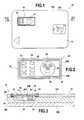
- FIG. 1shows an electronic device including a light source according to a first embodiment of the invention
- FIG. 2shows an enlarged scale top view of an electronic module of the device in FIG. 1 ;
- FIG. 3shows the section view along the line III-III in FIG. 1 ;
- FIG. 4is a detail perspective view of the light source shown in section in FIG. 3 ;
- FIG. 5shows the top view of FIG. 2 with some elements shown in transparency
- FIG. 6is a top view of another microcircuit card according to the invention.
- FIG. 7shows a section view of the card of FIG. 6 along the line 7 - 7 of the FIG. 6 .
- FIGS. 1 through 3An electronic device according to a first embodiment of the invention is shown in FIGS. 1 through 3 .
- the electronic device 10is labeled with the general reference number 10 .
- the electronic device 10is, in the embodiment described, a microcircuit card.
- the device 10can be a page of a passport such as the cover of the passport or even a self-adhesive label such as a sticker, etc.
- the device 10comprises a body 12 in the general shape of a card delimiting first 12 A and second 12 B opposite faces.
- the body 12defines the outside dimensions of the card 10 .
- the dimensions of the card 10are defined by the ID-1 format of the ISO 7816 standard which is the format used conventionally for banking card with dimensions of 86 millimeters by 54 millimeters.
- card formatscan also be used, such as the ID-000 format of the same standard for example.
- the card body 12is formed by lamination, that is by the formation, for example by means of a press and in a hot laminating operation, of a stack of laminated layers or sheets made for example of thermoplastic material.
- the body 12comprises a stack of at least three layers: a central layer 14 constituting a data printing layer interleaved between two preferably transparent external layers 16 A, 16 B.
- the body 12can be made in a single layer or of more than three layers.
- the body 12can be formed by molding, for example out of plastic.
- the device 10includes a microcircuit 15 capable of exchanging, processing and/or storing data.
- the body 12includes an electronic module 18 according to the invention.
- the microcircuit module 18is illustrated in detail in FIG. 2 .
- the module 18comprises a substrate 20 delimiting first 20 A and second 20 B opposite faces, the first face 20 A being designed to be visible from outside while the second face 20 B, opposite the first face 20 A, is designed to be masked when the module 18 is assembled within the device 10 .
- the body 12includes a cavity 22 for receiving this module 18 .
- the module 18once assembled within the device 10 , that is once housed in the cavity 22 , has a first outside face 20 A of the substrate 20 visible from the outside and a second inner face 20 B, opposite the first face 20 A, which is oriented to face a bottom 24 of the cavity 22 .
- the module 18is entirely incorporated into the body, for example in this case, the module is visible by transparency from part of the body at least.
- this variationis well suited to the case where the device is a passport or possibly a sticker.
- the module 18also includes a light source 26 borne by the second face 20 B of the substrate 20 and capable of illuminating through the substrate 20 , a part of the device visible from outside the device, corresponding to the first face 20 A or a part of the first face 20 A.
- the arrangement of this light source 26allows backlighting of the substrate 20 .
- the substrate 20 of the module 18includes at least one region 28 for transmitting light 26 running through the substrate 20 .
- the transmission region 28may be made up of the whole substrate 20 .
- the region 28is for example translucent, even transparent to the light emitted by the source 26 .
- the source 26has an emission spectrum comprised preferably within the visible light range.
- the substrate 20is made of a material capable of transmitting light.
- the substrate 20is made for example of a material comprised substantially of glass-epoxy which is a material translucent to visible light.
- the substrate 20can be made of a material comprised essentially of PET, of Teflon, of polyimide, of polyester or of a mixture of these compounds.
- the light source 26is a light-emitting diode.
- a diode 26is an electronic component capable of emitting light when an electrical current passes through it.
- the diode 26is of the SMC (surface-mount component) type.
- SMCsurface-mount component
- a surface-mounted componentcan be applied to a substrate of a printed circuit by adhesive bonding, brazing or soldering, unlike a component provided with pins, the assembly whereof to the substrate requires making holes in the substrate to allow passage of the pins.
- the light source 26is arranged so as to illuminate the substrate 20 substantially by direct light.
- the light source 26consists of a component comprised of a first, light-emitting part 26 A and a second part 26 B constituting an electrical connector of the component 26 with an external electronic circuit, such as for example a near-field communication antenna.
- the emitting part 26 Ais arranged at least partially facing the substrate 20 so as to illuminate the latter mainly with direct light (as opposed to reflected light).
- the emitting part 26 Ahas for instance the shape of a half-disc or a spherical cap or any other suitable shape.
- the connector part 26 Bconstitutes a contact plate equipped with two lateral connection terminals 27 and with a base 31 capable of being attached to the substrate 20 .
- the diode 26is assembled to the substrate 20 of the module 18 by soldering or brazing.
- the electronic module 18incorporates the microcircuit 15 of the card 10 .
- the card 10also comprises an external interface 32 of contact pads 34 electrically connected to the microcircuit 15 .
- This interface 32allows the establishment of contact communication, for example when the card 10 is inserted into a matching card reader.
- This interface 32comprises for example a series of metal electrical contact pads 34 complying with a predefined microcircuit card standard.
- the pads 34are compliant with the ISO 7816 standard.
- the pads 34 of the interface 32correspond to the contacts C 1 through C 8 of the ISO 7816 standard.
- the interface 32 of the card 10is preferably made of a layer of metallic material such as copper but may also be made, as a variation, by silkscreening with conductive ink of the epoxy filled with gold or silver particles type or by silkscreening of an electrically conductive polymer.
- the pads 34are electrically connected to the microcircuit 15 by electrically conductive wires (not shown) such as for example gold wires passing through vias made in the substrate 20 of the module 18 , connected in their turn to electrically conductive traces extending over the inner face 20 B of the substrate 20 . These traces have not been shown in FIG. 3 .
- the substrate 20also bears on its visible face 20 A a design 30 and the light source 26 is in this case preferably arranged so as to backlight the design 30 .
- the design 30covers at least partially the translucent region 28 of the substrate 20 .
- the light source 26extends preferably substantially in line with the design 30 , which allows the design 30 to be backlit when the light source 26 is supplied with power.
- the design 30 shown in this exampleis a face, preferably made of an electrically non-conductive material.
- the design 30is for example made by silkscreening with an electrically non-conductive ink.
- the design 30 in this illustrated examplehas apertures 29 through which the light is transmitted.
- the cavity 22comprises for example a deep central area provided with a bottom 24 for housing the microcircuit 15 and a peripheral area raised with respect to the central area delimiting a terrace 38 with the bottom 24 .
- the peripheral areacomprises a supporting surface raised with respect to the bottom 24 of the cavity 22 on which rest the edges of the substrate 20 of the module 18 .
- Such a cavity 22is generally obtained by machining, typically by milling or spot facing in two operations:
- the card 10is of the dual type, that is to say that it includes both a contactless interface capable of establishing near-field communication with an external terminal and a contact interface 32 capable of establishing communication with another external terminal by contact.
- the card 10can be solely of the contactless type. In this case, the card 10 is preferably not equipped with the external contact interface 32 .
- the device 10For establishing contactless communication with an external terminal, such as an external reader, the device 10 also includes a near-field communication antenna 40 .
- This antenna 40comprises for example a winding of electrically conductive turns comprising at least one turn.
- this antenna 40is connected to the microcircuit 15 to supply it with power.
- the antenna 40is connected to the microcircuit 15 by electrically conductive traces, by metal-plated vias, by electrically conductive wires, etc. (see FIG. 5 ).
- the antenna 40is preferably also borne by the module 18 .
- the antenna 40is borne at least partially by one of the faces of the substrate 20 of the module 18 and preferably by both faces of the substrate 20 of the module 18 .
- the modulehas a substrate of generally oblong shape so that the antenna 40 can have an effective area corresponding substantially to the dimensions of the substrate.
- the substratehas dimensions of 17.8 by 27.2 millimeters and a thickness comprised between 100 and 200 micrometers.
- the antenna 40consists of a winding of turns surrounding the microcircuit and running along the periphery of the substrate 20 .
- the antenna 40extends over both faces 20 A, 20 B of the substrate 20 ( FIG. 2 ).
- the antenna 40is also connected to the light source 26 for supplying the latter with power (for example by means identical with those used for the electrical connection of the microcircuit 15 , see also FIG. 5 ). More precisely, the antenna 40 and the diode 26 are configured so that the diode 26 emits light when a current of predefined intensity circulates in the antenna 40 , that is when near-field communication is established with an external contactless card reader.
- the configuration of the antenna circuit consisting of the assembly of the microcircuit 15 , the antenna 40 and the diode 26is defined by the configuration parameters selected among a wire length of the antenna 40 , a spacing between two turns of the antenna 40 , a wire width of the antenna 40 , a number of turns of the antenna 40 , as well as the capacitance of the semiconductor junction of the diode 26 .
- the configuration parametersare thus adjusted so that the operating frequency of the antenna circuit allows near-field communication with an external card reader.
- the operating frequencyis tuned to 13.56 MHz as defined by the ISO 14443 standard.
- the light source 26can be placed directly within the body 12 .
- the light source 26is arranged at the bottom of the cavity 22 .
- the device 10comprises first and second near-field communication antennas designed respectively to supply the microcircuit 15 and the light source 26 with power.
- each of the antennasis borne by one of the faces of the module's substrate.
- the user of the card 10is distant from an external contactless reading terminal.
- electromagnetic coupling between the antenna of the terminal and the antenna 40 of the card 10occurs.
- a current of nonzero intensitythen circulates in the antenna circuit.
- the microcircuitis supplied with power, allowing establishment of communication and the diode 26 , through which the current also passes, illuminates.
- the design 30is then backlit, which gives an indication to the user that the establishment of contactless communication took place successfully.
- the backlighting of the moduleproduces an esthetic and high quality effect while being particularly simple to implement.
- Such a backlit modulehas a great advantage for dual cards but can also find various applications with other contact or contactless cards or other pocket or portable electronic devices.
- the light source usedcan be of any type, a diode for example.
- the emission spectrum of the light sourcecan be selected according to need, without being limited to the visible spectrum.
- FIG. 6A microcircuit card according to the invention is shown in FIG. 6 . This card is assigned the overall reference number 100 .
- the card 100comprises a body 120 in the general shape of a card delimiting first 120 A and second 120 B opposite faces.
- the body 120delimits on its periphery an edge 140 of the card 100 . This edge is defined as being the outer peripheral edge surrounding the card 100 .
- the body 120delimits the outer dimensions of the card 100 .
- the dimensions of the cardare defined by the ID-1 format of the ISO 7816 standard which is the format conventionally used for banking cards with dimensions of 86 millimeters by 54 millimeters.
- ID-1 format of the ISO 7816 standardwhich is the format conventionally used for banking cards with dimensions of 86 millimeters by 54 millimeters.
- other card formatscan be used within the scope of the invention, such as for example the ID-000 card format of the same standard.
- the body 120incorporates the indicator light 160 (or light source 160 ) capable of at least partially illuminating the edge 140 of the card 100 , from the inside. The illuminated part is visible from outside the card.
- the body 120comprises at least one region 180 capable of transmitting, in the thickness of the card, the light emitted by the indicator light 160 .
- the luminous means 160is arranged within the body 120 to illuminate the edge 140 of the card 100 by way of this transmission region 180 .
- the transmission region 180is made of a first material and at least partially surrounded by a second material different from the first material.
- the body 120consists of a stack of layers extending through the body 120 and the transmission region 180 constitutes one of the layers of the stack.
- the body 120comprises a stack of at least three layers: a central layer 180 constituting a transmission region interleaved between at least two external layers 200 A, 200 B made of the second material, these two external layers constituting a so called peripheral region.
- the body 120is formed by lamination, that is by formation, for example by means of a press and in a hot laminating operation, of the stack of layers or laminated sheets made for example of a thermoplastic material.
- the body 120can be formed by molding, from plastic for example.
- the materialsare chosen so that the transmission and peripheral regions 180 , 200 A, 200 B constitute an optical waveguide in at least one direction.
- the transmission layer 180is made for example of polycarbonate. Possibly, the layer can also be made of a material supplied as a film of glass fibers such as compounds of the LGF (Light Guide Film) type based for example on polyurethane or acrylic.
- LGFLight Guide Film
- peripheral layers 200 A, 200 B surrounding the polycarbonate layerare made of PVC (polyvinyl chloride).
- the material of the transmission layer 180has an index of refraction greater than the index of refraction of the materials constituting the two external layers 200 A, 200 B surrounding the transmission layer 180 .
- the means 160emits in the visible spectrum.
- the two external layers 200 A, 200 Bare opaque. This makes it possible in particular to highlight the illumination of the edge of the card 10 .
- the luminous means 160is optically concealed between the two faces 120 A, 120 B of the card 100 .
- the luminous means 160is preferably arranged inside the transmission region 180 .
- the card 100comprises a microcircuit 220 capable of exchanging, processing and/or storing data.
- the body 12includes a microcircuit module 240 incorporating the microcircuit 220 .
- the body 120includes a cavity 260 for receiving the module 240 , this cavity 26 being made at least partially within the thickness of the transmission region 180 , so that the luminous means 160 extends at least partially into the transmission region 180 when the module 240 is housed in the cavity 260 .
- the module 240comprises a substrate 280 delimiting an outer face 280 A designed to be visible and a masked inner face 280 B designed to be facing the cavity 260 and bearing the microcircuit 220 as well as the luminous means 160 .
- the luminous means 160is optically hidden within the card between the two faces 120 A, 120 B of the card 10 .
- the luminous means 160can be observed from the edge 140 of the card 100 .
- an optical maskcan be arranged on the substrate 280 substantially in line with the luminous means 160 .
- a designcan for example be printed on the visible face 280 A of the substrate 280 to mask the light emitted by the source 160 .
- an opaque substrate 280can also be selected.
- the illumination of the module 240 by the source 160can also be exploited to contribute an additional esthetic or technical effect.
- the card 100is of the dual type, that is it allows both contact communication and contactless communication.
- the microcircuit module 240also includes a contact interface 30 electrically connected to the microcircuit 220 .
- This interfaceallows the establishment of contact communication by the card 100 , when the latter is inserted into a matching card reader.
- the interface 100is for example borne by the outer face 280 A of the substrate 280 of the module 240 .
- This interface 300comprises for example a series of metal electrical contact pads 320 , complying with a predefined microcircuit card standard.
- the contact padsare compliant with the ISO 7816 standard.
- the contact pads 320 of the interface 300correspond to the contacts C 1 through C 8 of the ISO 7816 standard.
- the interface 300 of the card 100is preferably made of a layer of metallic material such as copper, but can also be made, as a variation, by silkscreening of conductive ink of the type consisting of epoxy ink filled with particles of silver or gold or by silkscreening of an electrically conductive polymer.
- the padsare electrically connected to the microcircuit by electrically conductive wires such as for example gold wires passing through vias made in the substrate of the module, connected in their turn to electrically conductive connecting traces extending over the inner face of the substrate. These traces have not been shown in FIG. 7 .
- the card 100For establishing contactless communication with an external terminal, such as an external reader, the card 100 also includes at least one near-field communication antenna 340 .
- the antenna 340is preferably connected to the microcircuit 220 and is able to supply power to the microcircuit 220 by electromagnetic coupling with an external terminal (not shown).
- the communication frequency of the microcircuit with the external terminalis preferably the 13.56 MHz communication frequency defined by the ISO 14 443 standard.
- the antenna 340is also connected to the indicator light 160 to supply it with power.
- the card 100includes a first and second antennas connected respectively to the microcircuit 220 and to the luminous means 160 .
- the antenna 340extends into the interior of the module 240 .
- the antenna 340extends over the substrate 280 , for example on the two opposite faces of the substrate, so that the antenna 340 is partially visible from the outside.
- the light source 160is a light-emitting diode.
- a diodeis an electronic component capable of emitting light when an electrical current passes through it.
- the diodeis of the SMC or surface-mount component type.
- a surface-mount componentcan be applied to the substrate of a printed circuit by adhesive bonding, by brazing or by soldering, unlike a component provided with pins, the assembly whereof to the substrate requires making holes in the substrate to allow passage of the pins.
- the diode 160is assembled to the substrate 280 of the module 240 by brazing.
- the antenna 340is connected to the luminous means 160 and in this case the luminous means 160 is supplied with power by the antenna 340 .
- the luminous means 160is electrically connected to an external power supply contact extending over the card 100 , for example one of the power supply contacts of the interface 300 of contacts 320 .
- the luminous means 160is capable of being controlled according to the communication state of the microcircuit 220 , for example according to the state of a transaction.
- the card 100can be solely of the contactless type; in this case, the card 100 is preferably not equipped with the external contact interface. In another variation, the card 100 can be solely of the contact type and in this case, the card 100 is not equipped with the near-field communication antenna.
- the card 100can include at least two luminous means.
- the two luminous meanscan be controlled according to first and second communication states of the microcircuit.
- the userclearly perceives the change in color of the card since the latter is illuminated along its edge.
- FIGS. 6 and 7The principal aspects of the card's operation illustrated by FIGS. 6 and 7 will now be described.
- the useris out of range of the external contact terminal.
- the cardWhen he moves the card close to the external terminal, the card illuminates along the edge. This change in state of the card is immediately perceived by the user.
- the indicator lightis supplied with power via the contact interface 300 and the edge of the part of the card extending outside the card reader is also illuminated.
- the luminous meanscan be incorporated into the body.
- the luminous meansis connected to a near-field communication antenna to supply it with power, the assembly being arranged on one layer of a stack of layers laminated together constituting the body of the card.
Landscapes
- Engineering & Computer Science (AREA)
- Computer Hardware Design (AREA)
- Microelectronics & Electronic Packaging (AREA)
- Physics & Mathematics (AREA)
- General Physics & Mathematics (AREA)
- Theoretical Computer Science (AREA)
- Computer Networks & Wireless Communication (AREA)
- Credit Cards Or The Like (AREA)
Abstract
Description
This Application claims priority to French patent application no. 10/56974, filed on Sep. 2, 2010, and no. 10/56975, also filed on Sep. 2, 2010, both of which are hereby incorporated by reference in their entireties.
The present invention relates to a module for an electronic device and an electronic device including such a module.
The invention applies particularly to any type of portable or pocket electronic device capable of incorporating such a module, such as a USB key, an RFID (Radio Frequency Identification) tag, a chip card, etc.
The invention applies more particularly but not exclusively to microcircuit cards equipped with an antenna, such as the so-called contactless cards allowing establishment of contactless communication with an external terminal at a predefined communication frequency, such as for example the 13.56 MHz frequency defined by the ISO 14 443 standard.
It also applies to the so-called hybrid or dual cards allowing, in addition to the establishment of contactless communication, communication with contact through an external contact interface capable of making contact with a suitable reader.
Generally, the module comprises an electrically non-conductive substrate which bears the microcircuit on one of its faces and, in the case of contact type cards, an external contact interface on the opposite face, this interface being electrically connected to the microcircuit, through the substrate for example.
Dual cards generally comprise a body which incorporates the antenna as well as the electronic module, housed in a cavity provided in the body.
The antenna and the microcircuit are then conventionally connected electrically by means of metal studs during the interleaving of the module into the body.
Such a structural arrangement makes it possible to obtain relatively good communication range because the dimensions of the antenna are maximized within the limit of the dimensions of the card body. However, the connection of the microcircuit to the antenna has a certain number of disadvantages, particularly in terms of reliability and of production efficiency.
In order to correct these disadvantages, it is thus known to integrate the antenna directly into the electronic module, for example on the substrate bearing the microcircuit, and then to transfer the module into the body of the card using traditional interleaving techniques for conventional contact type cards.
Ordinarily, the dimensions of the substrate are limited to the dimensions of the interface of external contacts having a generally square or circular shape so that the substrate is entirely masked by the metal interface.
But the incorporation of the antenna into the module imposes a substantial increase in the dimensions of that substrate so that the antenna has an effective reception area for the magnetic field that is sufficient to maintain a satisfactory communication range.
However, in this case, a relatively large area of the substrate is not covered by the antenna and by the external contact interface, the antenna extending generally along the periphery of the substrate. This surface of substrate in the raw state produces a particularly unattractive effect in the card and gives an impression of poor quality manufacture.
The disclosed embodiments have the particular object of correcting these disadvantages. To this end, the disclosed embodiments have as their object an electronic module which is to be mounted on a cavity of the body of an electronic device, such as a microcircuit card, the module comprising a substrate delimiting first and second opposite faces, the first face being designed to be oriented towards the outside of the electronic device so that it is visible from outside the electronic device, the second face being designed to be oriented towards the bottom of the cavity, the module including a light source borne by the second face of the substrate and capable of lighting a part of the electronic device, said part being visible from outside said device.
The part of the device which is illuminated according to the disclosed embodiments of the invention may be a part of the module or another part of the electronic device.
Thus a first embodiment of the invention has as its object an electronic module for an electronic device such as a microcircuit card, comprising a substrate delimiting first and second opposite faces, the module comprising a luminous source borne by the second face of the substrate and capable of illuminating the first face through the substrate.
In this first embodiment of the invention, the luminous source makes it possible to backlight the module when it is supplied with power and noticeably improves the visual appearance of the device, a chip card for example, by producing a high quality effect. In addition, as the source is directly borne by the module, the manufacture of the card according to the invention is relatively simple and is compatible with conventional interleaving processes.
A module according to this first embodiment of the invention can also include one or more of the following features:
- the substrate includes a light transmission region extending between the two faces;
- the first face is designed to be visible and the second face is designed to be masked when the module is assembled within the electronic device;
- the substrate bears on the first face a design and the light source is arranged so as to backlight the design;
- the module includes a microcircuit borne on the second face of the substrate;
- the module includes an interface of external contacts connected to the microcircuit and borne by the first face of the substrate;
- the module comprises a near-field communication antenna connected to the microcircuit and borne by the module substrate;
- the substrate has a generally oblong shape;
- the light source comprises a light-emitting diode;
- the light source is arranged so as to illuminate the substrate by direct light;
- the light source consists of a component comprising a light-emitting part arranged at least partially facing the substrate;
- the substrate is made of a material consisting substantially of glass-epoxy.
The invention also has as its object an electronic device, such as a microcircuit card, comprising a module and a body provided with a cavity for receiving the module, the module is according to this first embodiment of the invention, the second face of the substrate being placed facing a bottom of the cavity.
The invention also has as its object an electronic device, such as a microcircuit card, comprising a module according to this first embodiment except in that this module does not include a light source, and a body provided with a cavity for receiving the module, the module comprising a substrate delimited by first and second opposite faces, the second face being arranged facing a bottom of the cavity, the device including a light source arranged within the body to light the first face of the substrate through said substrate.
In this case, by preference, the light source is placed at the bottom of the cavity.
Preferably, this device is a microcircuit card of the contactless, dual or contact type.
According to a second embodiment, the invention has as its object a module designed to be mounted on a microcircuit card to illuminate at least a part of an edge of said card.
This second embodiment of the invention exploits the fact that the majority of contact card readers leave the edge of the card exposed. The illumination of the edge is also especially esthetic and conspicuous. Indeed, when the edge of the card is illuminated, the user has a general impression of a color change in the card which is especially remarkable.
Preferably, the card can comprise two light sources having two distinct colors indicating two distinct communication states.
The invention also aims to a card incorporating a module according to this second embodiment.
A card according to this second embodiment of the invention can additionally include one or more of the following features:
- the body includes a region, capable of transmitting the light emitted by the luminous means, extending at least partially along the edge, the luminous means being arranged within the body so as to illuminate the edge of the body by way of this region;
- the transmission region is made of a first material and is surrounded at least partially by a second material, the materials being selected in such a way to constitute an optical waveguide in at least one direction;
- the body consisting of a stack of layers extending through the body, the transmission region constituting one of the layers of the stack;
- the luminous means is arranged within the transmission region;
- the luminous means is optically concealed between the first and second faces of the card;
- the card includes a module comprising the microcircuit and the luminous means, the body including a cavity for receiving the module;
- the cavity is made partially within the thickness of the transmission region so that the luminous means extends at least partially into the interior of the transmission region;
- the module comprises a substrate delimiting a first face designed to be visible and a second, opposite face destined to face the cavity, the second face bearing at least the luminous means;
- the card includes a near-field communication antenna connected to the microcircuit and to the luminous means;
- the card includes first and second near-field communication antennas connected respectively to the microcircuit and to the luminous means;
- the card includes a module comprising the microcircuit and the luminous means, the antenna or antennas being incorporated into the module;
- the luminous means is connected electrically to an external power supply contact extending over the card and capable of making contact with an external contact card reader;
- the luminous means is capable of being controlled according to the communication state of the microcircuit;
- the card includes first and second luminous means capable of being controlled according to the first and second communication states of the microcircuit;
- the card is a microcircuit card of the contactless, dual or contact type.
The device incorporating the module may have a thickness of 0.76 mm, (corresponding to ISO 7816 format) +/−10%.
Other features and advantages of the invention will appear in the light of the description that follows, made with reference to the appended drawings in which:
An electronic device according to a first embodiment of the invention is shown inFIGS. 1 through 3 .
This electronic device is labeled with thegeneral reference number 10. Theelectronic device 10 is, in the embodiment described, a microcircuit card. As a variation, thedevice 10 can be a page of a passport such as the cover of the passport or even a self-adhesive label such as a sticker, etc.
As illustrated inFIG. 1 , thedevice 10 comprises abody 12 in the general shape of a card delimiting first12A and second12B opposite faces.
In this embodiment, thebody 12 defines the outside dimensions of thecard 10. In this example and by preference, the dimensions of thecard 10 are defined by the ID-1 format of the ISO 7816 standard which is the format used conventionally for banking card with dimensions of 86 millimeters by 54 millimeters.
Of course, other card formats can also be used, such as the ID-000 format of the same standard for example.
Preferably, thecard body 12 is formed by lamination, that is by the formation, for example by means of a press and in a hot laminating operation, of a stack of laminated layers or sheets made for example of thermoplastic material.
For example, in this embodiment, thebody 12 comprises a stack of at least three layers: acentral layer 14 constituting a data printing layer interleaved between two preferably transparentexternal layers body 12 can be made in a single layer or of more than three layers.
As a variation, thebody 12 can be formed by molding, for example out of plastic. Conventionally, thedevice 10 includes amicrocircuit 15 capable of exchanging, processing and/or storing data.
More particularly, thebody 12 includes anelectronic module 18 according to the invention. Themicrocircuit module 18 is illustrated in detail inFIG. 2 . In conformity with the invention, themodule 18 comprises asubstrate 20 delimiting first20A and second20B opposite faces, thefirst face 20A being designed to be visible from outside while thesecond face 20B, opposite thefirst face 20A, is designed to be masked when themodule 18 is assembled within thedevice 10.
As shown inFIG. 3 , thebody 12 includes acavity 22 for receiving thismodule 18. Thus themodule 18, once assembled within thedevice 10, that is once housed in thecavity 22, has a firstoutside face 20A of thesubstrate 20 visible from the outside and a secondinner face 20B, opposite thefirst face 20A, which is oriented to face a bottom24 of thecavity 22.
In a variation not illustrated in the figures, themodule 18 is entirely incorporated into the body, for example in this case, the module is visible by transparency from part of the body at least. For example, this variation is well suited to the case where the device is a passport or possibly a sticker.
In this embodiment, themodule 18 also includes alight source 26 borne by thesecond face 20B of thesubstrate 20 and capable of illuminating through thesubstrate 20, a part of the device visible from outside the device, corresponding to thefirst face 20A or a part of thefirst face 20A. The arrangement of thislight source 26 allows backlighting of thesubstrate 20.
For example, thesubstrate 20 of themodule 18 includes at least oneregion 28 for transmitting light26 running through thesubstrate 20. Thetransmission region 28 may be made up of thewhole substrate 20. Theregion 28 is for example translucent, even transparent to the light emitted by thesource 26. Thesource 26 has an emission spectrum comprised preferably within the visible light range.
Preferably, thesubstrate 20 is made of a material capable of transmitting light.
For example, thesubstrate 20 is made for example of a material comprised substantially of glass-epoxy which is a material translucent to visible light. As a variation, thesubstrate 20 can be made of a material comprised essentially of PET, of Teflon, of polyimide, of polyester or of a mixture of these compounds.
Preferably, thelight source 26 is a light-emitting diode. As is known per se, adiode 26 is an electronic component capable of emitting light when an electrical current passes through it.
Preferably, thediode 26 is of the SMC (surface-mount component) type. Thus, in conventional fashion, a surface-mounted component can be applied to a substrate of a printed circuit by adhesive bonding, brazing or soldering, unlike a component provided with pins, the assembly whereof to the substrate requires making holes in the substrate to allow passage of the pins.
Preferably, thelight source 26 is arranged so as to illuminate thesubstrate 20 substantially by direct light.
A detail view of thelight source 26 is shown inFIG. 4 . In the example described, thelight source 26 consists of a component comprised of a first, light-emittingpart 26A and asecond part 26B constituting an electrical connector of thecomponent 26 with an external electronic circuit, such as for example a near-field communication antenna.
Preferably, the emittingpart 26A is arranged at least partially facing thesubstrate 20 so as to illuminate the latter mainly with direct light (as opposed to reflected light).
The emittingpart 26A has for instance the shape of a half-disc or a spherical cap or any other suitable shape. Theconnector part 26B constitutes a contact plate equipped with twolateral connection terminals 27 and with a base31 capable of being attached to thesubstrate 20.
In the example illustrated, thediode 26 is assembled to thesubstrate 20 of themodule 18 by soldering or brazing.
Preferably, in the preferred embodiment of the invention illustrated in the figures, theelectronic module 18 incorporates themicrocircuit 15 of thecard 10.
In this embodiment, thecard 10 also comprises anexternal interface 32 ofcontact pads 34 electrically connected to themicrocircuit 15. Thisinterface 32 allows the establishment of contact communication, for example when thecard 10 is inserted into a matching card reader.
Thisinterface 32 comprises for example a series of metalelectrical contact pads 34 complying with a predefined microcircuit card standard. For example, thepads 34 are compliant with the ISO 7816 standard. In this embodiment, thepads 34 of theinterface 32 correspond to the contacts C1 through C8 of the ISO 7816 standard.
Theinterface 32 of thecard 10 is preferably made of a layer of metallic material such as copper but may also be made, as a variation, by silkscreening with conductive ink of the epoxy filled with gold or silver particles type or by silkscreening of an electrically conductive polymer.
Preferably, thepads 34 are electrically connected to themicrocircuit 15 by electrically conductive wires (not shown) such as for example gold wires passing through vias made in thesubstrate 20 of themodule 18, connected in their turn to electrically conductive traces extending over theinner face 20B of thesubstrate 20. These traces have not been shown inFIG. 3 .
In the example described, thesubstrate 20 also bears on itsvisible face 20A adesign 30 and thelight source 26 is in this case preferably arranged so as to backlight thedesign 30.
Preferably, thedesign 30 covers at least partially thetranslucent region 28 of thesubstrate 20. In this case, thelight source 26 extends preferably substantially in line with thedesign 30, which allows thedesign 30 to be backlit when thelight source 26 is supplied with power.
Thedesign 30 shown in this example is a face, preferably made of an electrically non-conductive material. Thus, thedesign 30 is for example made by silkscreening with an electrically non-conductive ink. Thedesign 30 in this illustrated example hasapertures 29 through which the light is transmitted.
In addition, as illustrated inFIG. 3 and preferably, thecavity 22 comprises for example a deep central area provided with a bottom24 for housing themicrocircuit 15 and a peripheral area raised with respect to the central area delimiting aterrace 38 with the bottom24. The peripheral area comprises a supporting surface raised with respect to the bottom24 of thecavity 22 on which rest the edges of thesubstrate 20 of themodule 18.
Such acavity 22 is generally obtained by machining, typically by milling or spot facing in two operations:
- a large spot facing operation to form the peripheral area corresponding to the depth of the
terrace 38, - a small spot facing operation to form the deeper central area.
- a large spot facing operation to form the peripheral area corresponding to the depth of the
In the embodiment illustrated byFIGS. 1 through 3 , thecard 10 is of the dual type, that is to say that it includes both a contactless interface capable of establishing near-field communication with an external terminal and acontact interface 32 capable of establishing communication with another external terminal by contact. However, as a variation, thecard 10 can be solely of the contactless type. In this case, thecard 10 is preferably not equipped with theexternal contact interface 32.
For establishing contactless communication with an external terminal, such as an external reader, thedevice 10 also includes a near-field communication antenna 40. Thisantenna 40 comprises for example a winding of electrically conductive turns comprising at least one turn.
In the preferred embodiment of the invention, thisantenna 40 is connected to themicrocircuit 15 to supply it with power. For example, theantenna 40 is connected to themicrocircuit 15 by electrically conductive traces, by metal-plated vias, by electrically conductive wires, etc. (seeFIG. 5 ).
Theantenna 40 is preferably also borne by themodule 18. Thus, preferably, theantenna 40 is borne at least partially by one of the faces of thesubstrate 20 of themodule 18 and preferably by both faces of thesubstrate 20 of themodule 18.
As shown inFIG. 2 , it can be seen that the module has a substrate of generally oblong shape so that theantenna 40 can have an effective area corresponding substantially to the dimensions of the substrate. For example, the substrate has dimensions of 17.8 by 27.2 millimeters and a thickness comprised between 100 and 200 micrometers.
In addition, theantenna 40 consists of a winding of turns surrounding the microcircuit and running along the periphery of thesubstrate 20. For example, theantenna 40 extends over bothfaces FIG. 2 ).
Preferably, theantenna 40 is also connected to thelight source 26 for supplying the latter with power (for example by means identical with those used for the electrical connection of themicrocircuit 15, see alsoFIG. 5 ). More precisely, theantenna 40 and thediode 26 are configured so that thediode 26 emits light when a current of predefined intensity circulates in theantenna 40, that is when near-field communication is established with an external contactless card reader.
The configuration of the antenna circuit consisting of the assembly of themicrocircuit 15, theantenna 40 and thediode 26 is defined by the configuration parameters selected among a wire length of theantenna 40, a spacing between two turns of theantenna 40, a wire width of theantenna 40, a number of turns of theantenna 40, as well as the capacitance of the semiconductor junction of thediode 26.
The configuration parameters are thus adjusted so that the operating frequency of the antenna circuit allows near-field communication with an external card reader. For example, the operating frequency is tuned to 13.56 MHz as defined by the ISO 14443 standard.
In a second embodiment of the invention not shown in the figures, thelight source 26 can be placed directly within thebody 12. For example, thelight source 26 is arranged at the bottom of thecavity 22.
In a third embodiment of the invention not illustrated in the figures, thedevice 10 comprises first and second near-field communication antennas designed respectively to supply themicrocircuit 15 and thelight source 26 with power. For example, in this case, each of the antennas is borne by one of the faces of the module's substrate.
The principal aspects of the operation of thecard 10 ofFIGS. 1 through 3 will now be described.
Initially, the user of thecard 10 is distant from an external contactless reading terminal. When he comes close to the external terminal, electromagnetic coupling between the antenna of the terminal and theantenna 40 of thecard 10 occurs.
A current of nonzero intensity then circulates in the antenna circuit. The microcircuit is supplied with power, allowing establishment of communication and thediode 26, through which the current also passes, illuminates.
Thedesign 30 is then backlit, which gives an indication to the user that the establishment of contactless communication took place successfully.
The backlighting of the module produces an esthetic and high quality effect while being particularly simple to implement.
Thus, such a backlit module has a great advantage for dual cards but can also find various applications with other contact or contactless cards or other pocket or portable electronic devices.
In addition, the light source used can be of any type, a diode for example. The emission spectrum of the light source can be selected according to need, without being limited to the visible spectrum.
A microcircuit card according to the invention is shown inFIG. 6 . This card is assigned theoverall reference number 100.
As illustrated inFIG. 6 , thecard 100 comprises abody 120 in the general shape of a card delimiting first120A and second120B opposite faces. In addition, thebody 120 delimits on its periphery anedge 140 of thecard 100. This edge is defined as being the outer peripheral edge surrounding thecard 100.
In this embodiment, thebody 120 delimits the outer dimensions of thecard 100. In this example and by preference, the dimensions of the card are defined by the ID-1 format of the ISO 7816 standard which is the format conventionally used for banking cards with dimensions of 86 millimeters by 54 millimeters. Of course, other card formats can be used within the scope of the invention, such as for example the ID-000 card format of the same standard.
In conformity with this embodiment, thebody 120 incorporates the indicator light160 (or light source160) capable of at least partially illuminating theedge 140 of thecard 100, from the inside. The illuminated part is visible from outside the card.
To this end, preferably, thebody 120 comprises at least oneregion 180 capable of transmitting, in the thickness of the card, the light emitted by theindicator light 160. In other words, theluminous means 160 is arranged within thebody 120 to illuminate theedge 140 of thecard 100 by way of thistransmission region 180.
Preferably, thetransmission region 180 is made of a first material and at least partially surrounded by a second material different from the first material.
In this example, thebody 120 consists of a stack of layers extending through thebody 120 and thetransmission region 180 constitutes one of the layers of the stack.
As illustrated inFIG. 7 , thebody 120 comprises a stack of at least three layers: acentral layer 180 constituting a transmission region interleaved between at least twoexternal layers
Thus, preferably, thebody 120 is formed by lamination, that is by formation, for example by means of a press and in a hot laminating operation, of the stack of layers or laminated sheets made for example of a thermoplastic material.
Of course, in a variation that is not illustrated, thebody 120 can be formed by molding, from plastic for example.
The materials are chosen so that the transmission andperipheral regions
Thetransmission layer 180 is made for example of polycarbonate. Possibly, the layer can also be made of a material supplied as a film of glass fibers such as compounds of the LGF (Light Guide Film) type based for example on polyurethane or acrylic.
For example, theperipheral layers
Preferably, in order to optimize the optical guidance of the waves, the material of thetransmission layer 180 has an index of refraction greater than the index of refraction of the materials constituting the twoexternal layers transmission layer 180.
Preferably, themeans 160 emits in the visible spectrum.
Preferably, the twoexternal layers card 10.
In a preferred embodiment, theluminous means 160 is optically concealed between the twofaces card 100.
As illustrated inFIG. 7 , it is seen that theluminous means 160 is preferably arranged inside thetransmission region 180.
Thus, in the preferred embodiment of the invention, thecard 100 comprises amicrocircuit 220 capable of exchanging, processing and/or storing data. In a preferred embodiment, thebody 12 includes amicrocircuit module 240 incorporating themicrocircuit 220.
For example, preferably, thebody 120 includes acavity 260 for receiving themodule 240, thiscavity 26 being made at least partially within the thickness of thetransmission region 180, so that theluminous means 160 extends at least partially into thetransmission region 180 when themodule 240 is housed in thecavity 260.
For example, themodule 240 comprises asubstrate 280 delimiting anouter face 280A designed to be visible and a maskedinner face 280B designed to be facing thecavity 260 and bearing themicrocircuit 220 as well as theluminous means 160.
Thus, preferably, theluminous means 160 is optically hidden within the card between the twofaces card 10. However, the luminous means160 can be observed from theedge 140 of thecard 100.
In the case where thesubstrate 280 is translucent and allows the light of themeans 160 to pass, an optical mask can be arranged on thesubstrate 280 substantially in line with theluminous means 160. A design can for example be printed on thevisible face 280A of thesubstrate 280 to mask the light emitted by thesource 160. As a variation, anopaque substrate 280 can also be selected.
However, the illumination of themodule 240 by thesource 160 can also be exploited to contribute an additional esthetic or technical effect.
In the preferred embodiment of the invention, thecard 100 is of the dual type, that is it allows both contact communication and contactless communication.
To this end, themicrocircuit module 240 also includes acontact interface 30 electrically connected to themicrocircuit 220. This interface allows the establishment of contact communication by thecard 100, when the latter is inserted into a matching card reader. Theinterface 100 is for example borne by theouter face 280A of thesubstrate 280 of themodule 240.
Thisinterface 300 comprises for example a series of metalelectrical contact pads 320, complying with a predefined microcircuit card standard. For example, the contact pads are compliant with the ISO 7816 standard. In this embodiment, thecontact pads 320 of theinterface 300 correspond to the contacts C1 through C8 of the ISO 7816 standard.
Theinterface 300 of thecard 100 is preferably made of a layer of metallic material such as copper, but can also be made, as a variation, by silkscreening of conductive ink of the type consisting of epoxy ink filled with particles of silver or gold or by silkscreening of an electrically conductive polymer.
Preferably, the pads are electrically connected to the microcircuit by electrically conductive wires such as for example gold wires passing through vias made in the substrate of the module, connected in their turn to electrically conductive connecting traces extending over the inner face of the substrate. These traces have not been shown inFIG. 7 .
For establishing contactless communication with an external terminal, such as an external reader, thecard 100 also includes at least one near-field communication antenna 340.
In conformity with the invention, theantenna 340 is preferably connected to themicrocircuit 220 and is able to supply power to themicrocircuit 220 by electromagnetic coupling with an external terminal (not shown).
The communication frequency of the microcircuit with the external terminal is preferably the 13.56 MHz communication frequency defined by theISO 14 443 standard.
Preferably, theantenna 340 is also connected to the indicator light160 to supply it with power.
In one variation of the invention, thecard 100 includes a first and second antennas connected respectively to themicrocircuit 220 and to theluminous means 160. For example, theantenna 340 extends into the interior of themodule 240. Preferably, theantenna 340 extends over thesubstrate 280, for example on the two opposite faces of the substrate, so that theantenna 340 is partially visible from the outside.
Preferably, thelight source 160 is a light-emitting diode. As is known per se, a diode is an electronic component capable of emitting light when an electrical current passes through it. Preferably, the diode is of the SMC or surface-mount component type.
Thus, in conventional fashion, a surface-mount component can be applied to the substrate of a printed circuit by adhesive bonding, by brazing or by soldering, unlike a component provided with pins, the assembly whereof to the substrate requires making holes in the substrate to allow passage of the pins.
In the example illustrated inFIG. 7 , thediode 160 is assembled to thesubstrate 280 of themodule 240 by brazing. For example, theantenna 340 is connected to theluminous means 160 and in this case theluminous means 160 is supplied with power by theantenna 340.
In one variation, theluminous means 160 is electrically connected to an external power supply contact extending over thecard 100, for example one of the power supply contacts of theinterface 300 ofcontacts 320.
Preferably, theluminous means 160 is capable of being controlled according to the communication state of themicrocircuit 220, for example according to the state of a transaction.
As a variation, thecard 100 can be solely of the contactless type; in this case, thecard 100 is preferably not equipped with the external contact interface. In another variation, thecard 100 can be solely of the contact type and in this case, thecard 100 is not equipped with the near-field communication antenna.
In another embodiment of the invention not illustrated in the figures, thecard 100 can include at least two luminous means. For example, the two luminous means can be controlled according to first and second communication states of the microcircuit.
This makes it possible for the user to detect in a remarkable way two distinct communication states of the microcircuit which, in some applications, can allow a reduction in errors on the user's part in selecting applications, particularly when the card is operating in contact mode and is inserted into a card reader.
Indeed, in that case, the user clearly perceives the change in color of the card since the latter is illuminated along its edge.
The principal aspects of the card's operation illustrated byFIGS. 6 and 7 will now be described.
Initially, the user is out of range of the external contact terminal. When he moves the card close to the external terminal, the card illuminates along the edge. This change in state of the card is immediately perceived by the user.
In addition, when the user inserts the card in a contact card reader, the indicator light is supplied with power via thecontact interface 300 and the edge of the part of the card extending outside the card reader is also illuminated.
In particular, the luminous means can be incorporated into the body. For example, the luminous means is connected to a near-field communication antenna to supply it with power, the assembly being arranged on one layer of a stack of layers laminated together constituting the body of the card.
Claims (22)
1. A microcircuit module configured to be mounted in a cavity of a body of an electronic device, the module comprising a substrate delimiting first and second opposite faces, the first face being configured to be oriented towards an outside of the electronic device so that it is visible when the module is mounted in the cavity, the second face being configured to be oriented towards a bottom of the cavity when the module is mounted in the cavity, the module including a light source borne by the second face of the substrate and capable of lighting at least a part of the module, said part being visible from outside said device when the module is mounted in the cavity, the module further comprising a microcircuit borne by the second face of the substrate and a near-field communication antenna electrically connected to the microcircuit, the light source and the near-field communication antenna being configured so that the light source emits light when a current of a predefined intensity circulates in the antenna.
2. The module according to theclaim 1 , wherein the electronic device is a microcircuit card comprising in its thickness a transmission region through which the light emitted by the source can be transmitted, said light source being borne on said second face to illuminate at least a part of an edge of said card, this edge being perpendicular or almost perpendicular to said opposite faces when the module is disposed on said cavity.
3. A microcircuit card comprising a module according toclaim 2 , wherein said transmission region is made of a first material and surrounded at least partially by a second material different from the first material, the materials being selected to constitute an optical waveguide in at least one direction.
4. The card according toclaim 3 , wherein, the body consisting of a stack of layers extending through the body, the transmission region constituting one of the layers of the stack.
5. The card according toclaim 3 , wherein the light source is arranged within the transmission region.
6. The card according toclaim 5 , wherein the light source is optically concealed between the first and second faces of the card.
7. The card according toclaim 3 , wherein the cavity is made at least partially within the thickness of the transmission region so that the light source extends at least partially into the transmission region.
8. The card according toclaim 3 , wherein the light source is capable of being controlled according to a communication state of the microcircuit.
9. The card according toclaim 8 , including first and second light source capable of being controlled according to first and second communication states of the microcircuit.
10. The card according toclaim 3 , being a microcircuit card of the contactless, dual or contact type.
11. The module according toclaim 1 , wherein said substrate comprises a transmission region through which the light emitted by the source can be transmitted, said part visible from the outside of the device being a part of said first face.
12. The module according toclaim 11 , wherein the substrate bears on the first face a design and the light source is arranged so as to backlight the design.
13. The module according toclaim 11 , wherein the substrate has a generally oblong shape.
14. The module according toclaim 11 , wherein the substrate is made of a material comprised essentially of glass-epoxy, of polyimide, of Teflon, of polyester or of PET.
15. The module according toclaim 11 , wherein the light source is arranged so as to illuminate the substrate in direct light.
16. The module according toclaim 15 , wherein the light source consists of a component comprising a light-emitting part arranged at least partially facing the substrate.
17. The module according toclaim 1 , comprising an interface of external contracts electrically connected to the microcircuit and borne by the first face of the substrate.
18. The module according toclaim 1 , the module including first and second near-field communication antennas capable of supplying power to the microcircuit and the light source respectively.
19. The module according toclaim 1 including a near-field communication antenna capable of simultaneously supplying power to the microcircuit and the light source.
20. The module according toclaim 1 , wherein the light source comprises a light-emitting diode.
21. A microcircuit card, comprising a module and a body provided with a cavity for receiving the module, the module comprising a substrate delimiting first and second opposite faces, the second face being turned towards a bottom of said cavity, the device comprising a light source arranged within the body so as to light the first face of the substrate through said substrate, the module further comprising a microcircuit borne by the second face of the substrate and a near-field communication antenna electrically connected to the microcircuit, the light source and the near-field communication antenna being configured so that the light source emits light when a current of a predefined intensity circulates in the antenna; and wherein the light source is arranged at the bottom of the cavity.
22. The card according toclaim 21 , wherein the card is a microcircuit card of the contactless, dual or contact type.
Applications Claiming Priority (6)
| Application Number | Priority Date | Filing Date | Title |
|---|---|---|---|
| FR1056975AFR2964488B1 (en) | 2010-09-02 | 2010-09-02 | LIGHT MODULE FOR MICROCIRCUIT DEVICE |
| FR1056974AFR2964487B1 (en) | 2010-09-02 | 2010-09-02 | MICROCIRCUIT CARD COMPRISING A BRIGHT MEANS |
| FR1056974 | 2010-09-02 | ||
| FR10/56975 | 2010-09-02 | ||
| FR1056975 | 2010-09-02 | ||
| FR10/56974 | 2010-09-02 |
Publications (2)
| Publication Number | Publication Date |
|---|---|
| US20120055999A1 US20120055999A1 (en) | 2012-03-08 |
| US8517278B2true US8517278B2 (en) | 2013-08-27 |
Family
ID=44509071
Family Applications (1)
| Application Number | Title | Priority Date | Filing Date |
|---|---|---|---|
| US13/224,635ActiveUS8517278B2 (en) | 2010-09-02 | 2011-09-02 | Luminous module for microcircuit device |
Country Status (2)
| Country | Link |
|---|---|
| US (1) | US8517278B2 (en) |
| EP (1) | EP2426627B1 (en) |
Cited By (3)
| Publication number | Priority date | Publication date | Assignee | Title |
|---|---|---|---|---|
| US20160104064A1 (en)* | 2013-06-25 | 2016-04-14 | Toppan Printing Co., Ltd. | Ic module, dual ic card, and method for manufacturing ic module |
| US20170132507A1 (en)* | 2015-11-11 | 2017-05-11 | Mastercard International Incorporated | Integrated circuit card |
| FR3137476A1 (en)* | 2022-06-29 | 2024-01-05 | Idemia France | Microcircuit card comprising an insert with an LED between reflective films |
Families Citing this family (11)
| Publication number | Priority date | Publication date | Assignee | Title |
|---|---|---|---|---|
| JP5163776B2 (en)* | 2010-07-13 | 2013-03-13 | 株式会社デンソー | Card key |
| FR2964487B1 (en)* | 2010-09-02 | 2013-07-12 | Oberthur Technologies | MICROCIRCUIT CARD COMPRISING A BRIGHT MEANS |
| EP2426627B1 (en)* | 2010-09-02 | 2016-10-12 | Oberthur Technologies | Luminous module for a microcircuit device |
| JP5956944B2 (en)* | 2013-02-28 | 2016-07-27 | 日本電産サンキョー株式会社 | Non-contact information processing device |
| GB201413101D0 (en)* | 2014-07-23 | 2014-09-03 | Aprium Tech Ltd | Security Tag |
| US9297523B2 (en)* | 2014-08-13 | 2016-03-29 | Jill MacKay | LED stickers |
| DE102014016921A1 (en)* | 2014-11-17 | 2016-05-19 | Giesecke & Devrient Gmbh | Disk with a hidden tag |
| JP2018173877A (en)* | 2017-03-31 | 2018-11-08 | サトーホールディングス株式会社 | RFID card |
| SG11202109820RA (en)* | 2019-03-11 | 2021-10-28 | Ellipse World Inc | Packaged electronic module and manufacturing method thereof |
| FR3142580A1 (en) | 2022-11-25 | 2024-05-31 | Idemia France | Electronic document and method of ordering a transaction implemented by such a document |
| FR3157615A1 (en) | 2023-12-20 | 2025-06-27 | Idemia France | Microcircuit module intended to be mounted in a microcircuit card |
Citations (56)
| Publication number | Priority date | Publication date | Assignee | Title |
|---|---|---|---|---|
| JPS629487A (en)* | 1985-07-05 | 1987-01-17 | Matsushita Electric Ind Co Ltd | IC card |
| JPS62134780A (en)* | 1985-12-09 | 1987-06-17 | Hitachi Ltd | Contactless IC card |
| US4990759A (en)* | 1987-12-22 | 1991-02-05 | Gemplus Card International | Chip card structure |
| US5345367A (en)* | 1992-09-22 | 1994-09-06 | Intel Corporation | Thin form factor computer card |
| US5736727A (en)* | 1994-01-11 | 1998-04-07 | Nakata; Eiichi | IC communication card |
| US5959289A (en)* | 1996-02-13 | 1999-09-28 | Empire Airport Service Co., Ltd. | Card and information recording card and method of using the same |
| US6193156B1 (en)* | 1998-11-12 | 2001-02-27 | Wenyu Han | Method and apparatus for patterning cards, instruments and documents |
| US20010010333A1 (en)* | 1998-11-12 | 2001-08-02 | Wenyu Han | Method and apparatus for patterning cards, instruments and documents |
| US20020033419A1 (en)* | 2000-09-06 | 2002-03-21 | Didier Solirenne | Access control card, particularly for access to an automotive vehicle |
| US6406935B2 (en)* | 1999-11-29 | 2002-06-18 | Ask S.A. | Manufacturing process of a hybrid contact-contactless smart card with an antenna support made of fibrous material |
| US20020133713A1 (en)* | 2001-02-15 | 2002-09-19 | Jacques Fieschi | Security system for preventing a personal computer from being stolen or used by unauthorized people |
| US20030034400A1 (en)* | 1998-11-12 | 2003-02-20 | Wenyu Han | Method and apparatus for impeding the counterfeiting of discs |
| US20030052177A1 (en)* | 2001-09-14 | 2003-03-20 | Christophe Halope | Contactless or hybrid contact-contactless smart card with reinforced connection of the electronic module |
| US20030106935A1 (en)* | 2001-11-19 | 2003-06-12 | Burchette Robert L. | Transaction card system having security against unauthorized usage |
| US20030201331A1 (en)* | 1992-02-12 | 2003-10-30 | Alan Finkelstein | Wallet card with built-in light |
| JP2004094561A (en) | 2002-08-30 | 2004-03-25 | Toppan Printing Co Ltd | IC card |
| US6719206B1 (en)* | 1997-11-19 | 2004-04-13 | On Track Innovations Ltd. | Data transaction card and method of manufacture thereof |
| US6786419B2 (en)* | 2001-06-14 | 2004-09-07 | Ask S.A. | Contactless smart card with an antenna support and a chip support made of fibrous material |
| JP2004265176A (en) | 2003-03-03 | 2004-09-24 | Toppan Printing Co Ltd | IC card and information display method thereof |
| US20040222505A1 (en)* | 2001-08-09 | 2004-11-11 | Peter Laackman | Chip card having a projection mirror |
| WO2005027036A1 (en) | 2003-09-18 | 2005-03-24 | Nederlandse Organisatie Voor Toegepast- Natuurwetenschappelijk Onderzoek Tno | Identification card |
| US20050087606A1 (en)* | 2003-10-24 | 2005-04-28 | Datacard Corporation | Card edge marking |
| US20050139685A1 (en)* | 2003-12-30 | 2005-06-30 | Douglas Kozlay | Design & method for manufacturing low-cost smartcards with embedded fingerprint authentication system modules |
| WO2005071606A1 (en) | 2004-01-24 | 2005-08-04 | Kin Fai Kam | Activity reminder smart card |
| JP2005216044A (en)* | 2004-01-30 | 2005-08-11 | Seiko Precision Inc | Non-contact ic card and holder for non-contact ic card |
| JP2005293181A (en)* | 2004-03-31 | 2005-10-20 | Tsutsui Akio | Contactless ic card case |
| US20060060656A1 (en)* | 2004-09-21 | 2006-03-23 | Michael Waters | Light card |
| US20060124753A1 (en)* | 2004-12-14 | 2006-06-15 | International Business Machines Corporation | Smart card and method for its production |
| US20060289632A1 (en)* | 1998-12-30 | 2006-12-28 | Walker Jay S | Method and apparatus for promoting the selection and use of a transaction card |
| EP1847946A2 (en) | 2002-11-15 | 2007-10-24 | Sony Corporation | Data memory |
| US20070272761A1 (en)* | 1997-10-08 | 2007-11-29 | Gemplus | Method for making smart cards capable of operating with and without contact |
| US20080054077A1 (en) | 2006-08-29 | 2008-03-06 | Bellsouth Intellectual Property Corporation | Transactional cards with sensory features |
| US20080217414A1 (en)* | 2007-03-09 | 2008-09-11 | Oki Data Corporation | Flexible display member and article having the same |
| US20080223937A1 (en)* | 2007-03-15 | 2008-09-18 | Joseph Frank Preta | Smart apparatus for making secure transactions |
| US20080282540A1 (en) | 2007-05-14 | 2008-11-20 | Innovatier, Inc. | Method for making advanced smart cards with integrated electronics using isotropic thermoset adhesive materials with high quality exterior surfaces |
| US20080296606A1 (en)* | 2005-03-22 | 2008-12-04 | Stephane Ottobon | Electronic Module and Chip Card With Indicator Light |
| US20090015411A1 (en)* | 2007-07-10 | 2009-01-15 | Winner Industries (Shenzhen) Co., Ltd. | Medical products |
| US20090065589A1 (en)* | 2005-09-22 | 2009-03-12 | Setec Oy | Smartcard and method of producing smartcards |
| US20090109701A1 (en)* | 2007-10-31 | 2009-04-30 | Foxsemicon Integrated Technology, Inc. | Illuminant business card |
| US20090159712A1 (en)* | 2007-12-24 | 2009-06-25 | Dynamics Inc. | Payment cards and devices with displays, chips, rfids, magnetic emulators, magentic decoders, and other components |
| US20090167495A1 (en) | 2007-12-31 | 2009-07-02 | Smith Joshua R | Radio frequency identification tags adapted for localization and state indication |
| US20090206164A1 (en)* | 2005-08-19 | 2009-08-20 | Stefan Kluge | Card-shaped data carrier |
| US20090245029A1 (en)* | 2004-01-24 | 2009-10-01 | Kin Fai Kam | Activity reminder smart card |
| US20090315320A1 (en)* | 2006-09-26 | 2009-12-24 | Advanced Microelectronic And Automation Technology Ltd. | Inlays for security documents |
| US20100001077A1 (en)* | 2005-08-19 | 2010-01-07 | Stefan Kluge | Card-shaped data carrier |
| WO2010007287A1 (en) | 2008-06-24 | 2010-01-21 | Arjowiggins Security | Structure comprising a watermark or pseudo-watermark and integrated microcircuit device |
| US20100176205A1 (en)* | 2007-03-29 | 2010-07-15 | Smart Packaging Solutions (Sps) | Chip card with dual communication interface |
| US20100224685A1 (en)* | 2009-03-03 | 2010-09-09 | Casio Computer Co., Ltd. | Ic card capable of communicating with external device by utilizing electromagnetic induction |
| US20100308976A1 (en)* | 2007-10-26 | 2010-12-09 | Gemalto Sa | Radiofrequency communication device including a timer |
| US20110025463A1 (en)* | 2009-08-03 | 2011-02-03 | Atmel Corporation | Parallel Antennas for Contactless Device |
| US20110037607A1 (en)* | 2009-08-11 | 2011-02-17 | Oberthur Technologies | Microcircuit Card Comprising a Light-Emitting Diode |
| US20110174874A1 (en)* | 2010-01-19 | 2011-07-21 | Poznansky Amir | Transaction Card With Improved Security Features |
| US20120037710A1 (en)* | 2010-08-03 | 2012-02-16 | Oberthur Technologies | Microcircuit Device including a Near-Field Communication Antenna Circuit |
| US20120055999A1 (en)* | 2010-09-02 | 2012-03-08 | Oberthur Technologies | Luminous Module for Microcircuit Device |
| US20120061476A1 (en)* | 2010-09-02 | 2012-03-15 | Oberthur Technologies | Microcircuit Card Including a Luminous Means |
| US20120138691A1 (en)* | 2010-12-06 | 2012-06-07 | Oberthur Technologies | Method of receiving a module in a smart card body |
- 2011
- 2011-08-31EPEP11179466.5Apatent/EP2426627B1/enactiveActive
- 2011-09-02USUS13/224,635patent/US8517278B2/enactiveActive
Patent Citations (57)
| Publication number | Priority date | Publication date | Assignee | Title |
|---|---|---|---|---|
| JPS629487A (en)* | 1985-07-05 | 1987-01-17 | Matsushita Electric Ind Co Ltd | IC card |
| JPS62134780A (en)* | 1985-12-09 | 1987-06-17 | Hitachi Ltd | Contactless IC card |
| US4990759A (en)* | 1987-12-22 | 1991-02-05 | Gemplus Card International | Chip card structure |
| US20030201331A1 (en)* | 1992-02-12 | 2003-10-30 | Alan Finkelstein | Wallet card with built-in light |
| US5345367A (en)* | 1992-09-22 | 1994-09-06 | Intel Corporation | Thin form factor computer card |
| US5736727A (en)* | 1994-01-11 | 1998-04-07 | Nakata; Eiichi | IC communication card |
| US5959289A (en)* | 1996-02-13 | 1999-09-28 | Empire Airport Service Co., Ltd. | Card and information recording card and method of using the same |
| US20070272761A1 (en)* | 1997-10-08 | 2007-11-29 | Gemplus | Method for making smart cards capable of operating with and without contact |
| US6719206B1 (en)* | 1997-11-19 | 2004-04-13 | On Track Innovations Ltd. | Data transaction card and method of manufacture thereof |
| US20030034400A1 (en)* | 1998-11-12 | 2003-02-20 | Wenyu Han | Method and apparatus for impeding the counterfeiting of discs |
| US6193156B1 (en)* | 1998-11-12 | 2001-02-27 | Wenyu Han | Method and apparatus for patterning cards, instruments and documents |
| US20010010333A1 (en)* | 1998-11-12 | 2001-08-02 | Wenyu Han | Method and apparatus for patterning cards, instruments and documents |
| US20060289632A1 (en)* | 1998-12-30 | 2006-12-28 | Walker Jay S | Method and apparatus for promoting the selection and use of a transaction card |
| US6406935B2 (en)* | 1999-11-29 | 2002-06-18 | Ask S.A. | Manufacturing process of a hybrid contact-contactless smart card with an antenna support made of fibrous material |
| US6547135B2 (en)* | 2000-09-06 | 2003-04-15 | Siemens Automotive | Access control card, particularly for access to an automotive vehicle |
| US20020033419A1 (en)* | 2000-09-06 | 2002-03-21 | Didier Solirenne | Access control card, particularly for access to an automotive vehicle |
| US20020133713A1 (en)* | 2001-02-15 | 2002-09-19 | Jacques Fieschi | Security system for preventing a personal computer from being stolen or used by unauthorized people |
| US6786419B2 (en)* | 2001-06-14 | 2004-09-07 | Ask S.A. | Contactless smart card with an antenna support and a chip support made of fibrous material |
| US20040222505A1 (en)* | 2001-08-09 | 2004-11-11 | Peter Laackman | Chip card having a projection mirror |
| US20030052177A1 (en)* | 2001-09-14 | 2003-03-20 | Christophe Halope | Contactless or hybrid contact-contactless smart card with reinforced connection of the electronic module |
| US20030106935A1 (en)* | 2001-11-19 | 2003-06-12 | Burchette Robert L. | Transaction card system having security against unauthorized usage |
| JP2004094561A (en) | 2002-08-30 | 2004-03-25 | Toppan Printing Co Ltd | IC card |
| EP1847946A2 (en) | 2002-11-15 | 2007-10-24 | Sony Corporation | Data memory |
| JP2004265176A (en) | 2003-03-03 | 2004-09-24 | Toppan Printing Co Ltd | IC card and information display method thereof |
| WO2005027036A1 (en) | 2003-09-18 | 2005-03-24 | Nederlandse Organisatie Voor Toegepast- Natuurwetenschappelijk Onderzoek Tno | Identification card |
| US20050087606A1 (en)* | 2003-10-24 | 2005-04-28 | Datacard Corporation | Card edge marking |
| US20050139685A1 (en)* | 2003-12-30 | 2005-06-30 | Douglas Kozlay | Design & method for manufacturing low-cost smartcards with embedded fingerprint authentication system modules |
| WO2005071606A1 (en) | 2004-01-24 | 2005-08-04 | Kin Fai Kam | Activity reminder smart card |
| US20090245029A1 (en)* | 2004-01-24 | 2009-10-01 | Kin Fai Kam | Activity reminder smart card |
| JP2005216044A (en)* | 2004-01-30 | 2005-08-11 | Seiko Precision Inc | Non-contact ic card and holder for non-contact ic card |
| JP2005293181A (en)* | 2004-03-31 | 2005-10-20 | Tsutsui Akio | Contactless ic card case |
| US20060060656A1 (en)* | 2004-09-21 | 2006-03-23 | Michael Waters | Light card |
| US20060124753A1 (en)* | 2004-12-14 | 2006-06-15 | International Business Machines Corporation | Smart card and method for its production |
| US20080296606A1 (en)* | 2005-03-22 | 2008-12-04 | Stephane Ottobon | Electronic Module and Chip Card With Indicator Light |
| US20100001077A1 (en)* | 2005-08-19 | 2010-01-07 | Stefan Kluge | Card-shaped data carrier |
| US20090206164A1 (en)* | 2005-08-19 | 2009-08-20 | Stefan Kluge | Card-shaped data carrier |
| US20090065589A1 (en)* | 2005-09-22 | 2009-03-12 | Setec Oy | Smartcard and method of producing smartcards |
| US20080054077A1 (en) | 2006-08-29 | 2008-03-06 | Bellsouth Intellectual Property Corporation | Transactional cards with sensory features |
| US20090315320A1 (en)* | 2006-09-26 | 2009-12-24 | Advanced Microelectronic And Automation Technology Ltd. | Inlays for security documents |
| US20080217414A1 (en)* | 2007-03-09 | 2008-09-11 | Oki Data Corporation | Flexible display member and article having the same |
| US20080223937A1 (en)* | 2007-03-15 | 2008-09-18 | Joseph Frank Preta | Smart apparatus for making secure transactions |
| US20100176205A1 (en)* | 2007-03-29 | 2010-07-15 | Smart Packaging Solutions (Sps) | Chip card with dual communication interface |
| US20080282540A1 (en) | 2007-05-14 | 2008-11-20 | Innovatier, Inc. | Method for making advanced smart cards with integrated electronics using isotropic thermoset adhesive materials with high quality exterior surfaces |
| US20090015411A1 (en)* | 2007-07-10 | 2009-01-15 | Winner Industries (Shenzhen) Co., Ltd. | Medical products |
| US20100308976A1 (en)* | 2007-10-26 | 2010-12-09 | Gemalto Sa | Radiofrequency communication device including a timer |
| US20090109701A1 (en)* | 2007-10-31 | 2009-04-30 | Foxsemicon Integrated Technology, Inc. | Illuminant business card |
| US20090159712A1 (en)* | 2007-12-24 | 2009-06-25 | Dynamics Inc. | Payment cards and devices with displays, chips, rfids, magnetic emulators, magentic decoders, and other components |
| US20090167495A1 (en) | 2007-12-31 | 2009-07-02 | Smith Joshua R | Radio frequency identification tags adapted for localization and state indication |
| WO2010007287A1 (en) | 2008-06-24 | 2010-01-21 | Arjowiggins Security | Structure comprising a watermark or pseudo-watermark and integrated microcircuit device |
| US20100224685A1 (en)* | 2009-03-03 | 2010-09-09 | Casio Computer Co., Ltd. | Ic card capable of communicating with external device by utilizing electromagnetic induction |
| US20110025463A1 (en)* | 2009-08-03 | 2011-02-03 | Atmel Corporation | Parallel Antennas for Contactless Device |
| US20110037607A1 (en)* | 2009-08-11 | 2011-02-17 | Oberthur Technologies | Microcircuit Card Comprising a Light-Emitting Diode |
| US20110174874A1 (en)* | 2010-01-19 | 2011-07-21 | Poznansky Amir | Transaction Card With Improved Security Features |
| US20120037710A1 (en)* | 2010-08-03 | 2012-02-16 | Oberthur Technologies | Microcircuit Device including a Near-Field Communication Antenna Circuit |
| US20120055999A1 (en)* | 2010-09-02 | 2012-03-08 | Oberthur Technologies | Luminous Module for Microcircuit Device |
| US20120061476A1 (en)* | 2010-09-02 | 2012-03-15 | Oberthur Technologies | Microcircuit Card Including a Luminous Means |
| US20120138691A1 (en)* | 2010-12-06 | 2012-06-07 | Oberthur Technologies | Method of receiving a module in a smart card body |
Cited By (5)
| Publication number | Priority date | Publication date | Assignee | Title |
|---|---|---|---|---|
| US20160104064A1 (en)* | 2013-06-25 | 2016-04-14 | Toppan Printing Co., Ltd. | Ic module, dual ic card, and method for manufacturing ic module |
| US9633301B2 (en)* | 2013-06-25 | 2017-04-25 | Toppan Printing Co., Ltd. | IC module, dual IC card, and method for manufacturing IC module |
| US20170132507A1 (en)* | 2015-11-11 | 2017-05-11 | Mastercard International Incorporated | Integrated circuit card |
| US9760825B2 (en)* | 2015-11-11 | 2017-09-12 | Mastercard International Incorporated | Integrated circuit card |
| FR3137476A1 (en)* | 2022-06-29 | 2024-01-05 | Idemia France | Microcircuit card comprising an insert with an LED between reflective films |
Also Published As
| Publication number | Publication date |
|---|---|
| EP2426627A1 (en) | 2012-03-07 |
| US20120055999A1 (en) | 2012-03-08 |
| EP2426627B1 (en) | 2016-10-12 |
Similar Documents
| Publication | Publication Date | Title |
|---|---|---|
| US8517278B2 (en) | Luminous module for microcircuit device | |
| US8505827B2 (en) | Microcircuit card including a luminous means | |
| KR102210842B1 (en) | Improved lightable card | |
| TWI517052B (en) | Chip card containing active components | |
| KR102598204B1 (en) | Smart card with LED and manufacturing method thereof | |
| US20080296606A1 (en) | Electronic Module and Chip Card With Indicator Light | |
| KR101104026B1 (en) | Electronic card including piezoelectric circuit part for LED power supply | |
| US20110037607A1 (en) | Microcircuit Card Comprising a Light-Emitting Diode | |
| KR20220064910A (en) | Card inlay for direct connection or inductive coupling technology | |
| ES3028012T3 (en) | Electronic module with indication device | |
| US20090109701A1 (en) | Illuminant business card | |
| JP2024520698A (en) | Illuminated and weighted cards | |
| US11948034B2 (en) | Electronic card structure with decoration | |
| TWI861631B (en) | Luminescent electronic card | |
| KR100680186B1 (en) | Lighting card | |
| KR200388562Y1 (en) | The Emission Display RF Card by the use of the thin film LED module | |
| TWI785471B (en) | Metal, ceramic, or ceramic-coated transaction card with window or window pattern and optional backlighting | |
| CN221551237U (en) | Acrylic luminous intelligent card | |
| RU2793749C1 (en) | Card tab for direct connection or inductive coupling technology | |
| CN220795888U (en) | Luminous intelligent card and material in it module | |
| RU2818686C1 (en) | Payment smart card with contactless interface and light-emitting diodes (versions) | |
| FR2964488A1 (en) | Electronic module for use in e.g. chip card, has oblong shaped support comprising external face and internal face arranged opposite to bottom of cavity, where light source is carried by internal face and arranged for lighting external face | |
| US12313874B1 (en) | Light sculpture electronic card | |
| WO2024131394A1 (en) | Integrated circuit (ic) module, multi-interface ic card, and methods of forming same | |
| US20250299011A1 (en) | Smart card inlay element |
Legal Events
| Date | Code | Title | Description |
|---|---|---|---|
| AS | Assignment | Owner name:OBERTHUR TECHNOLOGIES, FRANCE Free format text:ASSIGNMENT OF ASSIGNORS INTEREST;ASSIGNORS:LE GARREC, LOIC;DUVAL, AGNES;VERE, DENIS;REEL/FRAME:027446/0179 Effective date:20110909 | |
| STCF | Information on status: patent grant | Free format text:PATENTED CASE | |
| FPAY | Fee payment | Year of fee payment:4 | |
| MAFP | Maintenance fee payment | Free format text:PAYMENT OF MAINTENANCE FEE, 8TH YEAR, LARGE ENTITY (ORIGINAL EVENT CODE: M1552); ENTITY STATUS OF PATENT OWNER: LARGE ENTITY Year of fee payment:8 | |
| AS | Assignment | Owner name:IDEMIA FRANCE, FRANCE Free format text:CHANGE OF NAME;ASSIGNOR:OBERTHUR TECHNOLOGIES;REEL/FRAME:062140/0907 Effective date:20180117 | |
| MAFP | Maintenance fee payment | Free format text:PAYMENT OF MAINTENANCE FEE, 12TH YEAR, LARGE ENTITY (ORIGINAL EVENT CODE: M1553); ENTITY STATUS OF PATENT OWNER: LARGE ENTITY Year of fee payment:12 |