US8516409B2 - Implementing vertical die stacking to distribute logical function over multiple dies in through-silicon-via stacked semiconductor device - Google Patents
Implementing vertical die stacking to distribute logical function over multiple dies in through-silicon-via stacked semiconductor deviceDownload PDFInfo
- Publication number
- US8516409B2 US8516409B2US12/944,020US94402010AUS8516409B2US 8516409 B2US8516409 B2US 8516409B2US 94402010 AUS94402010 AUS 94402010AUS 8516409 B2US8516409 B2US 8516409B2
- Authority
- US
- United States
- Prior art keywords
- die
- logic
- silicon
- circuit
- tsv
- Prior art date
- Legal status (The legal status is an assumption and is not a legal conclusion. Google has not performed a legal analysis and makes no representation as to the accuracy of the status listed.)
- Active, expires
Links
Images


Classifications
- H—ELECTRICITY
- H01—ELECTRIC ELEMENTS
- H01L—SEMICONDUCTOR DEVICES NOT COVERED BY CLASS H10
- H01L25/00—Assemblies consisting of a plurality of semiconductor or other solid state devices
- H01L25/03—Assemblies consisting of a plurality of semiconductor or other solid state devices all the devices being of a type provided for in a single subclass of subclasses H10B, H10D, H10F, H10H, H10K or H10N, e.g. assemblies of rectifier diodes
- H01L25/04—Assemblies consisting of a plurality of semiconductor or other solid state devices all the devices being of a type provided for in a single subclass of subclasses H10B, H10D, H10F, H10H, H10K or H10N, e.g. assemblies of rectifier diodes the devices not having separate containers
- H01L25/065—Assemblies consisting of a plurality of semiconductor or other solid state devices all the devices being of a type provided for in a single subclass of subclasses H10B, H10D, H10F, H10H, H10K or H10N, e.g. assemblies of rectifier diodes the devices not having separate containers the devices being of a type provided for in group H10D89/00
- H01L25/0657—Stacked arrangements of devices
- G—PHYSICS
- G11—INFORMATION STORAGE
- G11C—STATIC STORES
- G11C29/00—Checking stores for correct operation ; Subsequent repair; Testing stores during standby or offline operation
- G11C29/04—Detection or location of defective memory elements, e.g. cell constructio details, timing of test signals
- G11C29/08—Functional testing, e.g. testing during refresh, power-on self testing [POST] or distributed testing
- G11C29/12—Built-in arrangements for testing, e.g. built-in self testing [BIST] or interconnection details
- H—ELECTRICITY
- H01—ELECTRIC ELEMENTS
- H01L—SEMICONDUCTOR DEVICES NOT COVERED BY CLASS H10
- H01L25/00—Assemblies consisting of a plurality of semiconductor or other solid state devices
- H01L25/18—Assemblies consisting of a plurality of semiconductor or other solid state devices the devices being of the types provided for in two or more different main groups of the same subclass of H10B, H10D, H10F, H10H, H10K or H10N
- G—PHYSICS
- G11—INFORMATION STORAGE
- G11C—STATIC STORES
- G11C17/00—Read-only memories programmable only once; Semi-permanent stores, e.g. manually-replaceable information cards
- G11C17/14—Read-only memories programmable only once; Semi-permanent stores, e.g. manually-replaceable information cards in which contents are determined by selectively establishing, breaking or modifying connecting links by permanently altering the state of coupling elements, e.g. PROM
- G11C17/143—Read-only memories programmable only once; Semi-permanent stores, e.g. manually-replaceable information cards in which contents are determined by selectively establishing, breaking or modifying connecting links by permanently altering the state of coupling elements, e.g. PROM using laser-fusible links
- G—PHYSICS
- G11—INFORMATION STORAGE
- G11C—STATIC STORES
- G11C17/00—Read-only memories programmable only once; Semi-permanent stores, e.g. manually-replaceable information cards
- G11C17/14—Read-only memories programmable only once; Semi-permanent stores, e.g. manually-replaceable information cards in which contents are determined by selectively establishing, breaking or modifying connecting links by permanently altering the state of coupling elements, e.g. PROM
- G11C17/16—Read-only memories programmable only once; Semi-permanent stores, e.g. manually-replaceable information cards in which contents are determined by selectively establishing, breaking or modifying connecting links by permanently altering the state of coupling elements, e.g. PROM using electrically-fusible links
- G—PHYSICS
- G11—INFORMATION STORAGE
- G11C—STATIC STORES
- G11C2229/00—Indexing scheme relating to checking stores for correct operation, subsequent repair or testing stores during standby or offline operation
- G11C2229/70—Indexing scheme relating to G11C29/70, for implementation aspects of redundancy repair
- G11C2229/76—Storage technology used for the repair
- G11C2229/763—E-fuses, e.g. electric fuses or antifuses, floating gate transistors
- G—PHYSICS
- G11—INFORMATION STORAGE
- G11C—STATIC STORES
- G11C2229/00—Indexing scheme relating to checking stores for correct operation, subsequent repair or testing stores during standby or offline operation
- G11C2229/70—Indexing scheme relating to G11C29/70, for implementation aspects of redundancy repair
- G11C2229/76—Storage technology used for the repair
- G11C2229/766—Laser fuses
- G—PHYSICS
- G11—INFORMATION STORAGE
- G11C—STATIC STORES
- G11C29/00—Checking stores for correct operation ; Subsequent repair; Testing stores during standby or offline operation
- G11C29/70—Masking faults in memories by using spares or by reconfiguring
- G11C29/78—Masking faults in memories by using spares or by reconfiguring using programmable devices
- G11C29/785—Masking faults in memories by using spares or by reconfiguring using programmable devices with redundancy programming schemes
- G—PHYSICS
- G11—INFORMATION STORAGE
- G11C—STATIC STORES
- G11C29/00—Checking stores for correct operation ; Subsequent repair; Testing stores during standby or offline operation
- G11C29/70—Masking faults in memories by using spares or by reconfiguring
- G11C29/78—Masking faults in memories by using spares or by reconfiguring using programmable devices
- G11C29/80—Masking faults in memories by using spares or by reconfiguring using programmable devices with improved layout
- G11C29/802—Masking faults in memories by using spares or by reconfiguring using programmable devices with improved layout by encoding redundancy signals
- G—PHYSICS
- G11—INFORMATION STORAGE
- G11C—STATIC STORES
- G11C5/00—Details of stores covered by group G11C11/00
- G11C5/02—Disposition of storage elements, e.g. in the form of a matrix array
- G11C5/04—Supports for storage elements, e.g. memory modules; Mounting or fixing of storage elements on such supports
- H—ELECTRICITY
- H01—ELECTRIC ELEMENTS
- H01L—SEMICONDUCTOR DEVICES NOT COVERED BY CLASS H10
- H01L2224/00—Indexing scheme for arrangements for connecting or disconnecting semiconductor or solid-state bodies and methods related thereto as covered by H01L24/00
- H01L2224/01—Means for bonding being attached to, or being formed on, the surface to be connected, e.g. chip-to-package, die-attach, "first-level" interconnects; Manufacturing methods related thereto
- H01L2224/10—Bump connectors; Manufacturing methods related thereto
- H01L2224/12—Structure, shape, material or disposition of the bump connectors prior to the connecting process
- H01L2224/13—Structure, shape, material or disposition of the bump connectors prior to the connecting process of an individual bump connector
- H01L2224/13001—Core members of the bump connector
- H01L2224/1302—Disposition
- H01L2224/13025—Disposition the bump connector being disposed on a via connection of the semiconductor or solid-state body
- H—ELECTRICITY
- H01—ELECTRIC ELEMENTS
- H01L—SEMICONDUCTOR DEVICES NOT COVERED BY CLASS H10
- H01L2224/00—Indexing scheme for arrangements for connecting or disconnecting semiconductor or solid-state bodies and methods related thereto as covered by H01L24/00
- H01L2224/01—Means for bonding being attached to, or being formed on, the surface to be connected, e.g. chip-to-package, die-attach, "first-level" interconnects; Manufacturing methods related thereto
- H01L2224/10—Bump connectors; Manufacturing methods related thereto
- H01L2224/15—Structure, shape, material or disposition of the bump connectors after the connecting process
- H01L2224/16—Structure, shape, material or disposition of the bump connectors after the connecting process of an individual bump connector
- H01L2224/161—Disposition
- H01L2224/16135—Disposition the bump connector connecting between different semiconductor or solid-state bodies, i.e. chip-to-chip
- H01L2224/16145—Disposition the bump connector connecting between different semiconductor or solid-state bodies, i.e. chip-to-chip the bodies being stacked
- H—ELECTRICITY
- H01—ELECTRIC ELEMENTS
- H01L—SEMICONDUCTOR DEVICES NOT COVERED BY CLASS H10
- H01L2225/00—Details relating to assemblies covered by the group H01L25/00 but not provided for in its subgroups
- H01L2225/03—All the devices being of a type provided for in the same main group of the same subclass of class H10, e.g. assemblies of rectifier diodes
- H01L2225/04—All the devices being of a type provided for in the same main group of the same subclass of class H10, e.g. assemblies of rectifier diodes the devices not having separate containers
- H01L2225/065—All the devices being of a type provided for in the same main group of the same subclass of class H10
- H01L2225/06503—Stacked arrangements of devices
- H01L2225/06513—Bump or bump-like direct electrical connections between devices, e.g. flip-chip connection, solder bumps
- H—ELECTRICITY
- H01—ELECTRIC ELEMENTS
- H01L—SEMICONDUCTOR DEVICES NOT COVERED BY CLASS H10
- H01L2225/00—Details relating to assemblies covered by the group H01L25/00 but not provided for in its subgroups
- H01L2225/03—All the devices being of a type provided for in the same main group of the same subclass of class H10, e.g. assemblies of rectifier diodes
- H01L2225/04—All the devices being of a type provided for in the same main group of the same subclass of class H10, e.g. assemblies of rectifier diodes the devices not having separate containers
- H01L2225/065—All the devices being of a type provided for in the same main group of the same subclass of class H10
- H01L2225/06503—Stacked arrangements of devices
- H01L2225/06541—Conductive via connections through the device, e.g. vertical interconnects, through silicon via [TSV]
- H01L2225/06544—Design considerations for via connections, e.g. geometry or layout
- H—ELECTRICITY
- H01—ELECTRIC ELEMENTS
- H01L—SEMICONDUCTOR DEVICES NOT COVERED BY CLASS H10
- H01L2225/00—Details relating to assemblies covered by the group H01L25/00 but not provided for in its subgroups
- H01L2225/03—All the devices being of a type provided for in the same main group of the same subclass of class H10, e.g. assemblies of rectifier diodes
- H01L2225/04—All the devices being of a type provided for in the same main group of the same subclass of class H10, e.g. assemblies of rectifier diodes the devices not having separate containers
- H01L2225/065—All the devices being of a type provided for in the same main group of the same subclass of class H10
- H01L2225/06503—Stacked arrangements of devices
- H01L2225/06555—Geometry of the stack, e.g. form of the devices, geometry to facilitate stacking
- H01L2225/06565—Geometry of the stack, e.g. form of the devices, geometry to facilitate stacking the devices having the same size and there being no auxiliary carrier between the devices
- H—ELECTRICITY
- H01—ELECTRIC ELEMENTS
- H01L—SEMICONDUCTOR DEVICES NOT COVERED BY CLASS H10
- H01L23/00—Details of semiconductor or other solid state devices
- H01L23/48—Arrangements for conducting electric current to or from the solid state body in operation, e.g. leads, terminal arrangements ; Selection of materials therefor
- H01L23/481—Internal lead connections, e.g. via connections, feedthrough structures
Definitions
- the present inventionrelates generally to the data processing field, and more particularly, relates to a method and circuit for implementing stacking to distribute a logical function over multiple dies in through-silicon-via stacked semiconductor devices, and a design structure on which the subject circuit resides.
- TSVThrough-Silicon-Via
- TSVThrough-Silicon-Via
- TSVthrough silicon via
- FIG. 1illustrates an integrated circuit die stack including a bottom die master or controller, and upper dies 0 - 3 and a pair of TSVs extending through each die 0 , die 1 , die 2 , and die 3 .
- the TSVsinterconnect all the dies in the die stack as illustrated in FIG. 1 , including a respective TSV coupled to INPUT [0:M ⁇ 1] and OUTPUT [0:N ⁇ 1].
- INPUT [0:M ⁇ 1]INPUT
- OUTPUT0:N ⁇ 1
- some TSValso are required to send a signal, for example, a command to a specific die.
- FIG. 2illustrates an additional respective dedicated TSV for sending signals, for example, commands to a specific die, such as coupled to the select inputs SEL 0 , SEL 1 , SEL 2 , and SEL 3 from a bottom die master or controller.
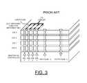
- FIG. 3further illustrates a laser fuse arrangement for fuse cutting different dies differently with a respective laser fuse connected to a respective TSV, which is coupled to the select inputs SEL 0 , SEL 1 , SEL 2 , and SEL 3 from the bottom die master or controller, which requires additional process or cost.
- Principal aspects of the present inventionare to provide a method and circuit for implementing die stacking to distribute a logical function over multiple dies in through-silicon-via stacked semiconductor devices, and a design structure on which the subject circuit resides.
- Other important aspects of the present inventionare to provide such method, circuit and design structure substantially without negative effects and that overcome many of the disadvantages of prior art arrangements.
- a method and circuit for implementing stacking to distribute a logical function over multiple dies, die identification and sparing in through-silicon-via stacked semiconductor devices, and a design structure on which the subject circuit residesare provided.
- Each die in the die stackincludes logic for implementing a respective predefined function.
- Each dieexecutes the respective predefined function and provides a respective functional result to an adjacent die in the die stack.
- each die in the die stackincludes logic for providing die identification.
- An operational die signatureis formed by combining a plurality of selected signals on each die.
- a die signatureis coupled to a next level adjacent die where it is logically combined with that die signature.
- the logic for providing die identificationincludes, for example, exclusive OR (XOR) logic for combining the plurality of selected signals on each die.
- XORexclusive OR
- the logic for providing die identificationincludes, for example, by shift register logic combining the plurality of selected signals on each die.
- a spare die in the die stackis used bypassing the identified de-selected die.
- spare die informationis stored in a fuse coupled to sparing logic.
- the fuse storing the spare die information coupled to the sparing logicis provided on a master semiconductor device in the die stack.
- FIGS. 1-3illustrate conventional prior art Through-Silicon-Via (TSV) arrangements used for various semiconductor chip stacking devices;
- TSVThrough-Silicon-Via
- FIG. 4schematically illustrates an exemplary circuit not to scale for implementing die identification in through-silicon-via stacked semiconductor devices in accordance with a preferred embodiment
- FIGS. 5 , 6 , and 7illustrate example combination logic of the exemplary circuit of FIG. 4 in accordance with a preferred embodiment
- FIG. 8schematically illustrates an exemplary circuit not to scale for implementing die sparing in through-silicon-via stacked semiconductor devices in accordance with a preferred embodiment
- FIGS. 9 , and 10illustrate example address logic of the exemplary circuit of FIG. 8 in accordance with a preferred embodiment
- FIG. 11schematically illustrates an exemplary circuit not to scale for implementing die identification in through-silicon-via stacked semiconductor devices in accordance with a preferred embodiment
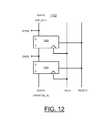
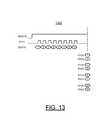
- FIGS. 12 , and 13illustrate example logic of the exemplary circuit of FIG. 11 in accordance with a preferred embodiment
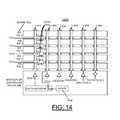
- FIG. 14schematically illustrates an exemplary circuit not to scale for implementing die sparing in through-silicon-via stacked semiconductor devices in accordance with a preferred embodiment
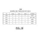
- FIGS. 15 , 16 , 17 , and 18illustrate example logic of the exemplary circuit of FIG. 14 in accordance with a preferred embodiment
- FIG. 19schematically illustrates an exemplary circuit not to scale for implementing die identification in through-silicon-via stacked semiconductor devices in accordance with a preferred embodiment
- FIG. 20schematically illustrates an exemplary circuit not to scale for implementing stacking to distribute a logical function over multiple dies in through-silicon-via stacked semiconductor devices in accordance with a preferred embodiment
- FIG. 21schematically illustrates an exemplary circuit not to scale for implementing stacking to distribute a logical adder function over multiple dies in through-silicon-via stacked semiconductor devices in accordance with a preferred embodiment
- FIG. 22schematically illustrates an exemplary circuit not to scale for implementing stacking to distribute a logical inverter function over multiple dies to constitute a ring oscillator in through-silicon-via stacked semiconductor devices in accordance with a preferred embodiment
- FIG. 23schematically illustrates an exemplary circuit not to scale for implementing stacking to distribute a logical built-in self-test (BIST) function over multiple dies in through-silicon-via stacked semiconductor devices in accordance with a preferred embodiment
- FIG. 24schematically illustrates an exemplary circuit not to scale for implementing stacking to distribute a logical built-in self-test (BIST) function over multiple dies in through-silicon-via stacked semiconductor devices;
- BISTlogical built-in self-test
- FIG. 25schematically illustrates an exemplary circuit not to scale for implementing stacking to distribute a logical arbiter or switcher function over multiple dies in through-silicon-via stacked semiconductor devices in accordance with a preferred embodiment
- FIG. 26schematically illustrates an exemplary circuit not to scale for implementing stacking to distribute a logical data processing function over multiple dies in through-silicon-via stacked semiconductor devices in accordance with a preferred embodiment
- FIG. 27is a flow diagram of a design process used in semiconductor design, manufacturing, and/or test.
- a method and circuit for implementing die identification and sparing in through-silicon-via stacked semiconductor devices, and a design structure on which the subject circuit residesare provided.
- Spare die informationis stored on a fuse coupled to sparing logic provided on a master semiconductor device in the die stack.
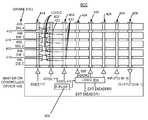
- Circuit 400includes a distributed logic generally designated by the reference character 402 respectively connected with packaging through silicon via (TSV) interconnections by the reference character 404 .
- the logic 402is distributed across a respective independent stacked integrated circuit die 406 , DIE 0 , DIE 1 , DIE 2 , and DIE 3 with a bottom master or controller device 408 in the circuit 400 .
- Each die 406 , DIE 0 , DIE 1 , DIE 2 , and DIE 3 in the die stack of circuit 400includes logic 402 for providing die identification.
- each stacked integrated circuit die 406 , DIE 0 , DIE 1 , DIE 2 , and DIE 3includes logic 402 containing an identical logic element contributing a partial solution based on state from the coupled die.
- circuit 400can include connections to a circuit board with interconnection pins providing the inputs and outputs or can terminate within the master or controller device 408 , as shown.
- the master or controller device 408may be identical to the stacked die, such as die 406 , DIE 0 , DIE 1 , DIE 2 , and DIE 3 or it may be a different die designed for a particular application as a master die or controller.
- An operational die signatureis formed by combining a plurality of selected signals on each die 406 , DIE 0 , DIE 1 , DIE 2 , and DIE 3 in circuit 400 .
- a die signatureis coupled from each respective die 406 to a next level adjacent die 406 , for example, from die 406 , DIE 0 to a next level adjacent 406 , DIE 1 , where it is logically combined with that die signature.
- a plurality of TSV interconnections 404 electrically connected to respective adjacent dies 406 , DIE 0 , DIE 1 , DIE 2 , and DIE 3is connected to a respective signal input DIEADDR 1 , DIEADDR 0 , INPUT [0:M ⁇ 1], and OUTPUT [0:N ⁇ 1] applied from the bottom master or controller device 408 .
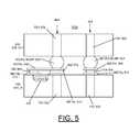
- FIGS. 5 , 6 , and 7illustrate example combination logic of the exemplary circuit 400 of FIG. 4 in accordance with a preferred embodiment.
- a pair of adjacent dies 406 , DIE_N and 406 , DIE_N+1is shown with a portion of an example pair of TSV interconnections 404 .
- Each TSV interconnection 404includes a respective TSV 502 extending through the illustrated adjacent dies 406 , DIE_N and 406 , DIE_N+1.
- a solder or micro-bump 504connects the TSV 502 of 406 , DIE_N+1 to an upper metal layer 506 .
- an electrically conductive via 508connects the upper metal layer 506 to a lower metal layer 510 connected to the TSV 502 of the die 406 , DIE_N.
- an intermetal dielectric layer 512electrically separates the upper metal layer 506 from the lower metal layer 510 connected to the TSV 502 of the die 406 , DIE_N.
- Logic 402is connected to the lower metal layer 510 connected to the TSV 502 of the die 406 , DIE_N and a second, spaced apart lower metal layer 510 connected by an electrically conductive via 508 to the upper metal layer 506 , which is connected by micro-bump 504 to the vertically aligned TSV 502 of 406 , DIE_N+1.
- example combination logicgenerally designated by the reference character 600 including logic 402 receiving inputs ID 1 [N] and ID 0 [N] and providing outputs ID 1 [N+1] and ID 0 [N+1].
- the combination logic 600includes a pair of exclusive OR gates (XOR) 602 respectively receiving inputs ID 1 [N] and ID 0 [N] and a respective signal input DIEADDR 1 , DIEADDR 0 , and providing outputs to a NOR gate 604 to identify a match, as shown.
- XORexclusive OR gates
- FIG. 7there is shown example inputs ID 1 [N] and ID 0 [N] and outputs ID 1 [N+1] and ID 0 [N+1] provided by the logic 402 of FIG. 6 .
- FIG. 8schematically illustrates an exemplary circuit not to scale for implementing die sparing in through-silicon-via stacked semiconductor devices generally designated by the reference character 800 in accordance with a preferred embodiment.
- Circuit 800includes a distributed logic generally designated by the reference character 802 respectively connected with packaging through silicon via (TSV) interconnections 404 .
- TSVthrough silicon via
- the logic 802is distributed across the respective independent stacked integrated circuit die 406 , DIE 0 , DIE 1 , DIE 2 , DIE 3 , and DIE 4 with the bottom master or controller device 408 in the circuit 800 , and sparing logic 804 to implement die sparing, when a de-selected die in the die stack is identified, a spare die in the die stack is used bypassing the identified de-selected die.
- the independent stacked integrated circuit die 406 , DIE 4is a spare die.
- a fuse or E-fuse 806 storing the spare die information, such as spare die 406 , DIE 4is coupled to the sparing logic 804 provided with the master semiconductor device 408 in the die stack.
- each stacked integrated circuit die 406 , DIE 0 , DIE 1 , DIE 2 , DIE 3 , and DIE 4includes logic 802 containing an identical logic element contributing a partial solution based on state from the coupled die.
- the distributed logic 802is connected to the three TSV interconnections 404 4 as indicated by arrows that include the dielectric layer 410 electrically separating respective adjacent dies 406 , DIE 0 , DIE 1 , DIE 2 , DIE 3 , and DIE.
- a plurality of TSV interconnections 404 electrically connected to respective adjacent dies 406 , DIE 0 , DIE 1 , DIE 2 , and DIE 3is connected to a respective signal input DIEADDR 2 , DIEADDR 1 , DIEADDR 0 , applied from sparing logic 804 and INPUT [0:M ⁇ 1], and OUTPUT [0:N ⁇ 1] from the bottom master or controller device 408 .
- FIGS. 9 , and 10illustrate example address logic 802 of the exemplary circuit 800 of FIG. 8 in accordance with a preferred embodiment.
- example inputs ID 2 [N], ID 1 [N] and ID 0 [N]address bits per each die 406 provided by the logic 802 of FIG. 8 .
- FIG. 10there is shown example external address inputs applied to sparing logic 804 and internal address inputs DIEADDR 2 , DIEADDR 1 , DIEADDR 0 with die address remapping with die 406 , DIE 2 de-selected provided by the logic 802 of FIG. 8 .
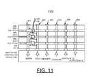
- FIG. 11schematically illustrates an exemplary circuit not to scale for implementing die identification in through-silicon-via stacked semiconductor devices generally designated by the reference character 1100 in accordance with a preferred embodiment.
- Circuit 1100includes a distributed logic generally designated by the reference character 1102 respectively connected with packaging through silicon via (TSV) interconnections by the reference character 404 .
- the logic 1102is distributed across the respective independent stacked integrated circuit die 406 , DIE 0 , DIE 1 , DIE 2 , and DIE 3 with the bottom master or controller device 408 in the circuit 400 .
- Each die 406 , DIE 0 , DIE 1 , DIE 2 , and DIE 3 in the die stack of circuit 1100includes logic 1102 for providing die identification.
- each stacked integrated circuit die 406 , DIE 0 , DIE 1 , DIE 2 , and DIE 3includes logic 1102 containing an identical logic element contributing a partial solution based on state from the coupled die.
- An operational die signatureis formed by combining a plurality of selected signals on each die 406 , DIE 0 , DIE 1 , DIE 2 , and DIE 3 in circuit 1100 , for example, with shift register logic 1102 .
- a die signatureis coupled from each respective die 406 to a next level adjacent die 406 , for example, from die 406 , DIE 0 to a next level adjacent 406 , DIE 1 , where it is logically combined with that die signature.
- a signal input SDATA coupled from the bottom master or controller device 408is applied to a first TSV interconnection 404 that include a dielectric layer 410 electrically separating respective adjacent dies 406 , DIE 0 , DIE 1 , DIE 2 , and DIE 3 .
- Electrical connections to and from the TSV interconnection 404 receiving signal input SDATA and the logic 1102 included in each die 406 , DIE 0 , DIE 1 , DIE 2 , and DIE 3are indicated by arrows.
- a plurality of TSV interconnections 404 electrically connected to respective adjacent dies 406 , DIE 0 , DIE 1 , DIE 2 , and DIE 3is connected to a respective signal input SCLK, DIEADDR 1 , DIEADDR 0 , INPUT [0:M ⁇ 1], and OUTPUT [0:N ⁇ 1] applied from the bottom master or controller device 408 .
- the signal input SCLKis applied to the logic 1102 included in each die 406 , DIE 0 , DIE 1 , DIE 2 , and DIE 3 are indicated by arrows.
- FIGS. 12 , and 13illustrate example logic 1102 of the exemplary circuit 1100 of FIG. 11 in accordance with a preferred embodiment.
- example combination logicgenerally designated by the reference character 1102 receiving inputs SDATA and SCLK, and RESET# and providing ID 1 [N] and ID 0 [N] outputs SDATA.
- the combination logic 1102includes a pair shift registers 1202 respectively receiving inputs SDATA and SCLK, and RESET#, as shown.
- FIG. 13there is shown example signals SDATA and SCLK, and RESET#, as shown, provided by the logic 1102 of FIGS. 11 and 12 .
- FIG. 14schematically illustrates an exemplary circuit not to scale for implementing die sparing in through-silicon-via stacked semiconductor devices generally designated by the reference character 1400 in accordance with a preferred embodiment.
- Circuit 1400includes a distributed logic generally designated by the reference character 1402 respectively connected with packaging through silicon via (TSV) interconnections 404 .
- TSVthrough silicon via
- the logic 1402is distributed across the respective independent stacked integrated circuit die 406 , DIE 0 , DIE 1 , DIE 2 , DIE 3 , and DIE 4 with the bottom master or controller device 408 in the circuit 1400 , and sparing SDATA register 1404 to implement die sparing, when a de-selected die in the die stack is identified, a spare die in the die stack is used bypassing the identified de-selected die.
- DIE 4is a spare die.
- a fuse or E-fuse 1406 storing the spare die information, such as spare die 406 , DIE 4is coupled to the sparing SDATA register 1404 provided with the master semiconductor device 408 in the die stack.
- FIGS. 15 , 16 , 17 , and 18illustrate example operation of SDATA register 1402 of the exemplary circuit 1400 of FIG. 14 in accordance with a preferred embodiment.
- FIG. 15illustrates example address example inputs ID 2 [N], ID 1 [N] and ID 0 [N] address bits per each die 406 and address inputs DIEADDR 1 and DIEADDR 0 with spare die 406 , DIE 4 not operated provided by the logic 1402 of the exemplary circuit 1400 in accordance with a preferred embodiment.
- FIG. 16there are shown example signals SDATA and SCLK, and RESET#, provided by the logic 1402 of FIG. 14 .
- FIG. 17there is shown example spare information stored in fuse 1406 and provided to the SDATA register 1404 of FIG. 14 .
- FIG. 18illustrates example address example inputs ID 2 [N], ID 1 [N] and ID 0 [N] address bits per each die 406 with die 1 replaced with die 4 .
- FIG. 19schematically illustrates an exemplary circuit not to scale for implementing die identification in through-silicon-via stacked semiconductor devices generally designated by the reference character 1900 in accordance with a preferred embodiment.
- Circuit 1900includes a distributed logic generally designated by the reference character 1902 respectively connected with packaging through silicon via (TSV) interconnections by the reference character 404 .
- the logic 1902is distributed across a respective independent stacked integrated circuit die 406 , DIE 0 , DIE 1 , DIE 2 , and DIE 3 in the circuit 1900 .
- a master die 406 , DIE 0includes controller die and die 406 , DIE 0 merged in this example master-slave structure with slaves die 406 , DIE 1 , DIE 2 , and DIE 3 .
- Each die 406 , DIE 0 , DIE 1 , DIE 2 , and DIE 3 in the die stack of circuit 400includes logic 402 for providing die identification.
- each stacked integrated circuit die 406 , DIE 0 , DIE 1 , DIE 2 , and DIE 3includes logic 402 containing an identical logic element contributing a partial solution based on state from the coupled die. In a die sparing case replacing DIE 0 with a spare die would provide the array part of DIE 0 not being used, while the controller part of master die 406 , DIE 0 would be used.
- An operational die signatureis formed by combining a plurality of selected signals on each die 406 , DIE 0 , DIE 1 , DIE 2 , and DIE 3 in circuit 400 .
- a die signatureis coupled from each respective die 406 to a next level adjacent die 406 , for example, from die 406 , DIE 0 to a next level adjacent 406 , DIE 1 , where it is logically combined with that die signature.
- a plurality of TSV interconnections 404 electrically connected to respective adjacent dies 406 , DIE 0 , DIE 1 , DIE 2 , and DIE 3is connected to a respective signal input DIEADDR 1 , DIEADDR 0 , INPUT [0:M ⁇ 1], and OUTPUT [0:N ⁇ 1] applied from the merged master die 406 , DIE 0 .
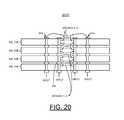
- FIG. 20schematically illustrates an exemplary circuit not to scale for implementing stacking to distribute a logical function over multiple dies in through-silicon-via stacked semiconductor devices generally designated by the reference character 2000 in accordance with a preferred embodiment.
- Circuit 2000includes a respective distributed logic function or stage generally designated by the reference character 2002 respectively connected with packaging through silicon via (TSV) interconnections by the reference character 404 .
- the respective logic stages 1, 2, 3, and 4, 2002is distributed across a respective independent stacked integrated circuit die 406 , DIE 0 , DIE 1 , DIE 2 , and DIE 3 in the circuit 2000 .
- a respective signal inputis coupled to a pair of TSV interconnections 404 that include a dielectric layer 410 electrically separating respective adjacent dies 406 , DIE 0 , DIE 1 , DIE 2 , and DIE 3 .
- a respective resultis coupled from each respective die 406 to a next level adjacent die 406 , for example, from die 406 , DIE 0 to a next level adjacent 406 , DIE 1 , where it is logically combined with the respective logic function or stage.
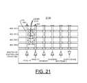
- FIG. 21schematically illustrates an exemplary circuit not to scale for implementing stacking to distribute a logical adder function over multiple dies in through-silicon-via stacked semiconductor devices generally designated by the reference character 2100 in accordance with a preferred embodiment.
- Circuit 2100includes a respective distributed adder function generally designated by the reference character 2102 respectively connected with packaging through silicon via (TSV) interconnections by the reference character 404 .
- the respective logical adder function 2102is distributed across a respective independent stacked integrated circuit die 406 , DIE 0 , DIE 1 , DIE 2 , and DIE 3 in the circuit 2100 .
- a respective adder resultis coupled from each respective die 406 to a next level adjacent die 406 , for example, from die 406 , DIE 0 to a next level adjacent 406 , DIE 1 , where it is logically combined with the respective adder function.
- FIG. 22schematically illustrates an exemplary circuit not to scale for implementing stacking to distribute a logical inverter function over multiple dies to constitute a ring oscillator in through-silicon-via stacked semiconductor devices generally designated by the reference character 2200 in accordance with a preferred embodiment.
- Circuit 2200includes a respective distributed logical inverter function generally designated by the reference character 2202 respectively connected with packaging through silicon via (TSV) interconnections by the reference character 404 .
- the respective logical inverter function 2202is distributed across a respective independent stacked integrated circuit die 406 , DIE 0 , DIE 1 , DIE 2 , and DIE 3 in the circuit 2200 .
- a respective signal inputis coupled to a TSV interconnection 404 that include a dielectric layer 410 electrically separating respective adjacent dies 406 , DIE 0 , DIE 1 , DIE 2 , and DIE 3 .
- a respective adder resultis coupled from each respective die 406 to a next level adjacent die 406 , for example, from die 406 , DIE 0 to a next level adjacent 406 , DIE 1 , where it is logically combined with the respective adder logical inverter function.
- FIG. 23schematically illustrates an exemplary circuit not to scale for implementing stacking to distribute a logical built-in self-test (BIST) function over multiple dies in through-silicon-via stacked semiconductor devices generally designated by the reference character 2300 in accordance with a preferred embodiment.
- Circuit 2300includes a respective distributed BIST 2302 providing a BIST result, labeled TEST GOOD, and receiving an input from a next level adjacent die 406 , #N ⁇ 1 and respectively connected by a respective logic gate 2304 to a next level adjacent die 406 , #N+1 with packaging through silicon via (TSV) interconnections 404 by schematically shown in FIG. 23 .
- TEST GOODlogical built-in self-test
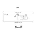
- FIG. 24schematically illustrates an exemplary circuit not to scale for implementing stacking to distribute a logical die signature function over multiple dies in through-silicon-via stacked semiconductor devices generally designated by the reference character 2400 in accordance with a preferred embodiment.
- Circuit 2400includes a respective distributed die signature 2402 providing a die signature result, labeled TEST GOOD, and receiving an input from a next level adjacent die 406 , #N ⁇ 1 and respectively connected by a respective logic exclusive or (XOR) gate 2404 to a next level adjacent die 406 , #N+1 with packaging through silicon via (TSV) interconnections schematically shown in FIG. 24 .
- TEST GOODa die signature result
- XORlogic exclusive or
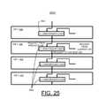
- FIG. 25schematically illustrates an exemplary circuit not to scale for implementing stacking to distribute a logical arbiter or switcher function over multiple dies in through-silicon-via stacked semiconductor devices generally designated by the reference character 2500 in accordance with a preferred embodiment.
- Circuit 2500includes a respective 2:1 arbiter/switcher function 2502 is distributed across a respective independent stacked integrated circuit die 406 , DIE 0 , DIE 1 , DIE 2 , and DIE 3 in the circuit 2500 .
- Each respective 2:1 arbiter/switcher function 2502receiving an input request from an adjacent die 406 , #N+1 and an input request from the current die 406 , #N and respectively connected by a respective 2:1 arbiter/switcher function 2502 of a next level adjacent die 406 , #N ⁇ 1 with packaging through silicon via (TSV) interconnections 404 schematically shown in FIG. 25 .
- TSVsilicon via
- FIG. 26schematically illustrates an exemplary circuit not to scale for implementing stacking to distribute a logical data processing function over multiple dies in through-silicon-via stacked semiconductor devices generally designated by the reference character 2600 in accordance with a preferred embodiment.
- Circuit 2600includes a plurality of stacked dies 406 .
- Each die 406 in the die stack circuit 2600includes a plurality of data processing units 2602 .
- Each respective vertically aligned DPU 2602is respectively connected by a DPU 2602 of a next level adjacent die 406 with packaging through silicon via (TSV) interconnections 404 schematically shown in FIG. 26 .
- TSVthrough silicon via
- FIG. 27is a flow diagram of a design process used in semiconductor design, manufacturing, and/or test.
- FIG. 27shows a block diagram of an example design flow 2700 .
- Design flow 2700may vary depending on the type of IC being designed. For example, a design flow 2700 for building an application specific IC (ASIC) may differ from a design flow 2700 for designing a standard component.
- Design structure 2702is preferably an input to a design process 2704 and may come from an IP provider, a core developer, or other design company or may be generated by the operator of the design flow, or from other sources.
- Design structure 2702comprises circuits 400 , 800 , 1100 , 1400 , 1900 , 2000 , 2100 , 2200 , 2300 , 2400 , 2500 , and 2600 in the form of schematics or HDL, a hardware-description language, for example, Verilog, VHDL, C, and the like.
- Design structure 2702may be contained on one or more machine readable medium.
- design structure 2702may be a text file or a graphical representation of circuits 400 , 800 , 1100 , 1400 , 1900 , 2000 , 2100 , 2200 , 2300 , 2400 , 2500 , and 2600 .
- Design process 2704preferably synthesizes, or translates, circuit 100 into a netlist 2706 , where netlist 2706 is, for example, a list of wires, transistors, logic gates, control circuits, I/O, models, etc. that describes the connections to other elements and circuits in an integrated circuit design and recorded on at least one of machine readable medium. This may be an iterative process in which netlist 2706 is resynthesized one or more times depending on design specifications and parameters for the circuits.
- Design process 2704may include using a variety of inputs; for example, inputs from library elements 2704 which may house a set of commonly used elements, circuits, and devices, including models, layouts, and symbolic representations, for a given manufacturing technology, such as different technology nodes, 42 nm, 45 nm, 90 nm, and the like, design specifications 2710 , characterization data 2712 , verification data 2714 , design rules 2716 , and test data files 2718 , which may include test patterns and other testing information. Design process 2704 may further include, for example, standard circuit design processes such as timing analysis, verification, design rule checking, place and route operations, and the like.
- standard circuit design processessuch as timing analysis, verification, design rule checking, place and route operations, and the like.
- Design process 2704preferably translates embodiments of the invention as shown in FIGS. 4-26 , along with any additional integrated circuit design or data (if applicable), into a second design structure 2720 .
- Design structure 2720resides on a storage medium in a data format used for the exchange of layout data of integrated circuits, for example, information stored in a GDSII (GDS2), GL1, OASIS, or any other suitable format for storing such design structures.
- Design structure 2720may comprise information such as, for example, test data files, design content files, manufacturing data, layout parameters, wires, levels of metal, vias, shapes, data for routing through the manufacturing line, and any other data required by a semiconductor manufacturer to produce an embodiment of the invention as shown in FIGS. 4-26 .
- Design structure 2720may then proceed to a stage 2722 where, for example, design structure 2720 proceeds to tape-out, is released to manufacturing, is released to a mask house, is sent to another design house, is sent back to the customer, and the like.
Landscapes
- Engineering & Computer Science (AREA)
- Microelectronics & Electronic Packaging (AREA)
- Power Engineering (AREA)
- Physics & Mathematics (AREA)
- Condensed Matter Physics & Semiconductors (AREA)
- General Physics & Mathematics (AREA)
- Computer Hardware Design (AREA)
- Design And Manufacture Of Integrated Circuits (AREA)
- Semiconductor Integrated Circuits (AREA)
Abstract
Description
Claims (4)
Priority Applications (1)
| Application Number | Priority Date | Filing Date | Title |
|---|---|---|---|
| US12/944,020US8516409B2 (en) | 2010-11-11 | 2010-11-11 | Implementing vertical die stacking to distribute logical function over multiple dies in through-silicon-via stacked semiconductor device |
Applications Claiming Priority (1)
| Application Number | Priority Date | Filing Date | Title |
|---|---|---|---|
| US12/944,020US8516409B2 (en) | 2010-11-11 | 2010-11-11 | Implementing vertical die stacking to distribute logical function over multiple dies in through-silicon-via stacked semiconductor device |
Publications (2)
| Publication Number | Publication Date |
|---|---|
| US20120124532A1 US20120124532A1 (en) | 2012-05-17 |
| US8516409B2true US8516409B2 (en) | 2013-08-20 |
Family
ID=46049005
Family Applications (1)
| Application Number | Title | Priority Date | Filing Date |
|---|---|---|---|
| US12/944,020Active2031-07-06US8516409B2 (en) | 2010-11-11 | 2010-11-11 | Implementing vertical die stacking to distribute logical function over multiple dies in through-silicon-via stacked semiconductor device |
Country Status (1)
| Country | Link |
|---|---|
| US (1) | US8516409B2 (en) |
Cited By (18)
| Publication number | Priority date | Publication date | Assignee | Title |
|---|---|---|---|---|
| US8732647B1 (en)* | 2013-03-13 | 2014-05-20 | Atrenta, Inc. | Method for creating physical connections in 3D integrated circuits |
| US9281302B2 (en) | 2014-02-20 | 2016-03-08 | International Business Machines Corporation | Implementing inverted master-slave 3D semiconductor stack |
| US10580757B2 (en) | 2016-10-07 | 2020-03-03 | Xcelsis Corporation | Face-to-face mounted IC dies with orthogonal top interconnect layers |
| US10580735B2 (en) | 2016-10-07 | 2020-03-03 | Xcelsis Corporation | Stacked IC structure with system level wiring on multiple sides of the IC die |
| US10586786B2 (en) | 2016-10-07 | 2020-03-10 | Xcelsis Corporation | 3D chip sharing clock interconnect layer |
| US10593667B2 (en) | 2016-10-07 | 2020-03-17 | Xcelsis Corporation | 3D chip with shielded clock lines |
| US10600691B2 (en) | 2016-10-07 | 2020-03-24 | Xcelsis Corporation | 3D chip sharing power interconnect layer |
| US10600780B2 (en) | 2016-10-07 | 2020-03-24 | Xcelsis Corporation | 3D chip sharing data bus circuit |
| US10600735B2 (en) | 2016-10-07 | 2020-03-24 | Xcelsis Corporation | 3D chip sharing data bus |
| US10607136B2 (en) | 2017-08-03 | 2020-03-31 | Xcelsis Corporation | Time borrowing between layers of a three dimensional chip stack |
| US10672743B2 (en)* | 2016-10-07 | 2020-06-02 | Xcelsis Corporation | 3D Compute circuit with high density z-axis interconnects |
| US10672744B2 (en)* | 2016-10-07 | 2020-06-02 | Xcelsis Corporation | 3D compute circuit with high density Z-axis interconnects |
| US10672745B2 (en) | 2016-10-07 | 2020-06-02 | Xcelsis Corporation | 3D processor |
| US10672663B2 (en) | 2016-10-07 | 2020-06-02 | Xcelsis Corporation | 3D chip sharing power circuit |
| US11289333B2 (en) | 2016-10-07 | 2022-03-29 | Xcelsis Corporation | Direct-bonded native interconnects and active base die |
| US11599299B2 (en) | 2019-11-19 | 2023-03-07 | Invensas Llc | 3D memory circuit |
| US20230197686A1 (en)* | 2021-12-17 | 2023-06-22 | Kioxia Corporation | Semiconductor memory device and method of manufacturing the same |
| US12308087B2 (en) | 2010-11-03 | 2025-05-20 | Netlist, Inc. | Memory package having stacked array dies and reduced driver load |
Families Citing this family (18)
| Publication number | Priority date | Publication date | Assignee | Title |
|---|---|---|---|---|
| KR101190682B1 (en)* | 2010-09-30 | 2012-10-12 | 에스케이하이닉스 주식회사 | Three dimensional stacked semiconductor integrated circuit |
| US8669780B2 (en)* | 2011-10-31 | 2014-03-11 | Taiwan Semiconductor Manufacturing Company, Ltd. | Three dimensional integrated circuit connection structure and method |
| US8624626B2 (en)* | 2011-11-14 | 2014-01-07 | Taiwan Semiconductor Manufacturing Co., Ltd. | 3D IC structure and method |
| KR101917718B1 (en)* | 2011-12-16 | 2018-11-14 | 에스케이하이닉스 주식회사 | Semiconductor integrated circuit |
| KR20140008174A (en)* | 2012-07-11 | 2014-01-21 | 에스케이하이닉스 주식회사 | Semiconductor chip module and semiconductor pacage having the same |
| US9472284B2 (en) | 2012-11-19 | 2016-10-18 | Silicon Storage Technology, Inc. | Three-dimensional flash memory system |
| US8817547B2 (en) | 2012-12-10 | 2014-08-26 | Micron Technology, Inc. | Apparatuses and methods for unit identification in a master/slave memory stack |
| US8957504B2 (en) | 2013-03-15 | 2015-02-17 | IP Enval Consultant Inc. | Integrated structure with a silicon-through via |
| US8952500B2 (en) | 2013-03-15 | 2015-02-10 | IPEnval Consultant Inc. | Semiconductor device |
| US9030025B2 (en) | 2013-03-15 | 2015-05-12 | IPEnval Consultant Inc. | Integrated circuit layout |
| US9406403B2 (en)* | 2013-06-25 | 2016-08-02 | Advanced Micro Devices, Inc. | Spare memory external to protected memory |
| KR20150043045A (en)* | 2013-10-14 | 2015-04-22 | 에스케이하이닉스 주식회사 | Semiconductor device |
| US9263157B2 (en) | 2013-12-23 | 2016-02-16 | International Business Machines Corporation | Detecting defective connections in stacked memory devices |
| KR20170066082A (en)* | 2015-12-04 | 2017-06-14 | 삼성전자주식회사 | Built-In Self-Test circuit, memory device including the same and operation method thereof |
| US10008287B2 (en)* | 2016-07-22 | 2018-06-26 | Micron Technology, Inc. | Shared error detection and correction memory |
| US10664432B2 (en) | 2018-05-23 | 2020-05-26 | Micron Technology, Inc. | Semiconductor layered device with data bus inversion |
| US10964702B2 (en) | 2018-10-17 | 2021-03-30 | Micron Technology, Inc. | Semiconductor device with first-in-first-out circuit |
| CN116344441B (en)* | 2023-02-03 | 2024-01-12 | 深圳华芯星半导体有限公司 | Chip packaging method and computer readable storage medium |
Citations (16)
| Publication number | Priority date | Publication date | Assignee | Title |
|---|---|---|---|---|
| US20050010725A1 (en)* | 2003-07-07 | 2005-01-13 | Eilert Sean E. | Method and apparatus for generating a device ID for stacked devices |
| US20090013291A1 (en)* | 2005-10-06 | 2009-01-08 | Synopsys, Inc. | Generating A Base Curve Database To Reduce Storage Cost |
| US20100023569A1 (en)* | 2008-07-22 | 2010-01-28 | Daw Shien Scientific Research & Development, Inc. | Method for computerized arithmetic operations |
| US20100131684A1 (en)* | 2008-11-26 | 2010-05-27 | Micron Technology, Inc. | Sharing resources in multi-dice stacks |
| US20100259296A1 (en)* | 2009-04-14 | 2010-10-14 | Zvi Or-Bach | Method for fabrication of a semiconductor device and structure |
| US20100295600A1 (en)* | 2009-05-20 | 2010-11-25 | Qualcomm Incorporated | Method and Apparatus for Providing Through Silicon VIA (TSV) Redundancy |
| US20110050320A1 (en)* | 2009-09-02 | 2011-03-03 | Mosaid Technologies Incorporated | Using interrupted through-silicon-vias in integrated circuits adapted for stacking |
| US20110110064A1 (en)* | 2009-11-12 | 2011-05-12 | International Business Machines Corporation | Integrating Circuit Die Stacks Having Initially Identical Dies Personalized With Fuses |
| US20110121838A1 (en)* | 2009-11-25 | 2011-05-26 | International Business Machines Corporation | Method and apparatus for increased effectiveness of delay and transistion fault testing |
| US20110182423A1 (en)* | 2007-12-10 | 2011-07-28 | Peter Lablans | Data Encryption and Decryption with a Key by an N-state Inverter Modified Switching Function |
| US20110194326A1 (en)* | 2010-02-11 | 2011-08-11 | Takuya Nakanishi | Memory dies, stacked memories, memory devices and methods |
| US20120019292A1 (en)* | 2010-06-28 | 2012-01-26 | Xilinx, Inc. | Configuration of a multi-die integrated circuit |
| US20120096218A1 (en)* | 2004-11-12 | 2012-04-19 | Ati Technologies Ulc | Apparatus and methods for tuning a memory interface |
| US20120194219A1 (en)* | 2005-02-16 | 2012-08-02 | Technion Research & Development Foundation Ltd. | Logic circuit and method of logic circuit design |
| US20120221907A1 (en)* | 1998-02-18 | 2012-08-30 | Texas Instruments Incorporated | Hierarchical access of test access ports in embedded core integrated circuits |
| US20120297262A1 (en)* | 2000-03-09 | 2012-11-22 | Texas Instruments Incorporated | Adapting scan-bist architectures for low power operation |
- 2010
- 2010-11-11USUS12/944,020patent/US8516409B2/enactiveActive
Patent Citations (16)
| Publication number | Priority date | Publication date | Assignee | Title |
|---|---|---|---|---|
| US20120221907A1 (en)* | 1998-02-18 | 2012-08-30 | Texas Instruments Incorporated | Hierarchical access of test access ports in embedded core integrated circuits |
| US20120297262A1 (en)* | 2000-03-09 | 2012-11-22 | Texas Instruments Incorporated | Adapting scan-bist architectures for low power operation |
| US20050010725A1 (en)* | 2003-07-07 | 2005-01-13 | Eilert Sean E. | Method and apparatus for generating a device ID for stacked devices |
| US20120096218A1 (en)* | 2004-11-12 | 2012-04-19 | Ati Technologies Ulc | Apparatus and methods for tuning a memory interface |
| US20120194219A1 (en)* | 2005-02-16 | 2012-08-02 | Technion Research & Development Foundation Ltd. | Logic circuit and method of logic circuit design |
| US20090013291A1 (en)* | 2005-10-06 | 2009-01-08 | Synopsys, Inc. | Generating A Base Curve Database To Reduce Storage Cost |
| US20110182423A1 (en)* | 2007-12-10 | 2011-07-28 | Peter Lablans | Data Encryption and Decryption with a Key by an N-state Inverter Modified Switching Function |
| US20100023569A1 (en)* | 2008-07-22 | 2010-01-28 | Daw Shien Scientific Research & Development, Inc. | Method for computerized arithmetic operations |
| US20100131684A1 (en)* | 2008-11-26 | 2010-05-27 | Micron Technology, Inc. | Sharing resources in multi-dice stacks |
| US20100259296A1 (en)* | 2009-04-14 | 2010-10-14 | Zvi Or-Bach | Method for fabrication of a semiconductor device and structure |
| US20100295600A1 (en)* | 2009-05-20 | 2010-11-25 | Qualcomm Incorporated | Method and Apparatus for Providing Through Silicon VIA (TSV) Redundancy |
| US20110050320A1 (en)* | 2009-09-02 | 2011-03-03 | Mosaid Technologies Incorporated | Using interrupted through-silicon-vias in integrated circuits adapted for stacking |
| US20110110064A1 (en)* | 2009-11-12 | 2011-05-12 | International Business Machines Corporation | Integrating Circuit Die Stacks Having Initially Identical Dies Personalized With Fuses |
| US20110121838A1 (en)* | 2009-11-25 | 2011-05-26 | International Business Machines Corporation | Method and apparatus for increased effectiveness of delay and transistion fault testing |
| US20110194326A1 (en)* | 2010-02-11 | 2011-08-11 | Takuya Nakanishi | Memory dies, stacked memories, memory devices and methods |
| US20120019292A1 (en)* | 2010-06-28 | 2012-01-26 | Xilinx, Inc. | Configuration of a multi-die integrated circuit |
Cited By (41)
| Publication number | Priority date | Publication date | Assignee | Title |
|---|---|---|---|---|
| US12308087B2 (en) | 2010-11-03 | 2025-05-20 | Netlist, Inc. | Memory package having stacked array dies and reduced driver load |
| US8732647B1 (en)* | 2013-03-13 | 2014-05-20 | Atrenta, Inc. | Method for creating physical connections in 3D integrated circuits |
| US9281302B2 (en) | 2014-02-20 | 2016-03-08 | International Business Machines Corporation | Implementing inverted master-slave 3D semiconductor stack |
| US10068886B2 (en) | 2014-02-20 | 2018-09-04 | International Business Machines Corporation | Implementing inverted master-slave 3D semiconductor stack |
| US10672663B2 (en) | 2016-10-07 | 2020-06-02 | Xcelsis Corporation | 3D chip sharing power circuit |
| US10886177B2 (en) | 2016-10-07 | 2021-01-05 | Xcelsis Corporation | 3D chip with shared clock distribution network |
| US10593667B2 (en) | 2016-10-07 | 2020-03-17 | Xcelsis Corporation | 3D chip with shielded clock lines |
| US10600691B2 (en) | 2016-10-07 | 2020-03-24 | Xcelsis Corporation | 3D chip sharing power interconnect layer |
| US10600780B2 (en) | 2016-10-07 | 2020-03-24 | Xcelsis Corporation | 3D chip sharing data bus circuit |
| US10600735B2 (en) | 2016-10-07 | 2020-03-24 | Xcelsis Corporation | 3D chip sharing data bus |
| US10580735B2 (en) | 2016-10-07 | 2020-03-03 | Xcelsis Corporation | Stacked IC structure with system level wiring on multiple sides of the IC die |
| US10672743B2 (en)* | 2016-10-07 | 2020-06-02 | Xcelsis Corporation | 3D Compute circuit with high density z-axis interconnects |
| US10672744B2 (en)* | 2016-10-07 | 2020-06-02 | Xcelsis Corporation | 3D compute circuit with high density Z-axis interconnects |
| US10672745B2 (en) | 2016-10-07 | 2020-06-02 | Xcelsis Corporation | 3D processor |
| US11823906B2 (en) | 2016-10-07 | 2023-11-21 | Xcelsis Corporation | Direct-bonded native interconnects and active base die |
| US12401010B2 (en) | 2016-10-07 | 2025-08-26 | Adeia Semiconductor Inc. | 3D processor having stacked integrated circuit die |
| US12362182B2 (en) | 2016-10-07 | 2025-07-15 | Adeia Semiconductor Inc. | Direct-bonded native interconnects and active base die |
| US10586786B2 (en) | 2016-10-07 | 2020-03-10 | Xcelsis Corporation | 3D chip sharing clock interconnect layer |
| US10892252B2 (en) | 2016-10-07 | 2021-01-12 | Xcelsis Corporation | Face-to-face mounted IC dies with orthogonal top interconnect layers |
| US10950547B2 (en) | 2016-10-07 | 2021-03-16 | Xcelsis Corporation | Stacked IC structure with system level wiring on multiple sides of the IC die |
| US10580757B2 (en) | 2016-10-07 | 2020-03-03 | Xcelsis Corporation | Face-to-face mounted IC dies with orthogonal top interconnect layers |
| US10978348B2 (en) | 2016-10-07 | 2021-04-13 | Xcelsis Corporation | 3D chip sharing power interconnect layer |
| US11152336B2 (en) | 2016-10-07 | 2021-10-19 | Xcelsis Corporation | 3D processor having stacked integrated circuit die |
| US12293993B2 (en) | 2016-10-07 | 2025-05-06 | Adeia Semiconductor Inc. | 3D chip sharing data bus |
| US11289333B2 (en) | 2016-10-07 | 2022-03-29 | Xcelsis Corporation | Direct-bonded native interconnects and active base die |
| US11557516B2 (en) | 2016-10-07 | 2023-01-17 | Adeia Semiconductor Inc. | 3D chip with shared clock distribution network |
| US12218059B2 (en) | 2016-10-07 | 2025-02-04 | Adeia Semiconductor Inc. | Stacked IC structure with orthogonal interconnect layers |
| US12142528B2 (en) | 2016-10-07 | 2024-11-12 | Adeia Semiconductor Inc. | 3D chip with shared clock distribution network |
| US11881454B2 (en) | 2016-10-07 | 2024-01-23 | Adeia Semiconductor Inc. | Stacked IC structure with orthogonal interconnect layers |
| US11824042B2 (en) | 2016-10-07 | 2023-11-21 | Xcelsis Corporation | 3D chip sharing data bus |
| US10607136B2 (en) | 2017-08-03 | 2020-03-31 | Xcelsis Corporation | Time borrowing between layers of a three dimensional chip stack |
| US11790219B2 (en) | 2017-08-03 | 2023-10-17 | Adeia Semiconductor Inc. | Three dimensional circuit implementing machine trained network |
| US12248869B2 (en) | 2017-08-03 | 2025-03-11 | Adeia Semiconductor Inc. | Three dimensional circuit implementing machine trained network |
| US11176450B2 (en) | 2017-08-03 | 2021-11-16 | Xcelsis Corporation | Three dimensional circuit implementing machine trained network |
| US10970627B2 (en) | 2017-08-03 | 2021-04-06 | Xcelsis Corporation | Time borrowing between layers of a three dimensional chip stack |
| US10762420B2 (en) | 2017-08-03 | 2020-09-01 | Xcelsis Corporation | Self repairing neural network |
| US10719762B2 (en) | 2017-08-03 | 2020-07-21 | Xcelsis Corporation | Three dimensional chip structure implementing machine trained network |
| US11599299B2 (en) | 2019-11-19 | 2023-03-07 | Invensas Llc | 3D memory circuit |
| US12293108B2 (en) | 2019-11-19 | 2025-05-06 | Adeia Semiconductor Technologies Llc | 3D memory circuit |
| US20230197686A1 (en)* | 2021-12-17 | 2023-06-22 | Kioxia Corporation | Semiconductor memory device and method of manufacturing the same |
| US12412870B2 (en)* | 2021-12-17 | 2025-09-09 | Kioxia Corporation | Semiconductor memory device and method of manufacturing the same |
Also Published As
| Publication number | Publication date |
|---|---|
| US20120124532A1 (en) | 2012-05-17 |
Similar Documents
| Publication | Publication Date | Title |
|---|---|---|
| US8516409B2 (en) | Implementing vertical die stacking to distribute logical function over multiple dies in through-silicon-via stacked semiconductor device | |
| US8060843B2 (en) | Verification of 3D integrated circuits | |
| US8856710B2 (en) | Tool and method for modeling interposer RC couplings | |
| US8522186B2 (en) | Method and apparatus of an integrated circuit | |
| US8904337B2 (en) | Semiconductor device design method, system and computer-readable medium | |
| US8890607B2 (en) | Stacked chip system | |
| CN104752415B (en) | Method and apparatus for three dimensional integrated circuits | |
| US8332803B1 (en) | Method and apparatus for integrated circuit package thermo-mechanical reliability analysis | |
| US11068636B2 (en) | Method for semiconductor package and semiconductor package design system | |
| CN107066681A (en) | The computer implemented method of integrated circuit and manufacture integrated circuit | |
| Kirihata et al. | Three-dimensional dynamic random access memories using through-silicon-vias | |
| US9064081B1 (en) | Generating database for cells routable in pin layer | |
| US11569219B2 (en) | TSV coupled integrated circuits and methods | |
| US8732647B1 (en) | Method for creating physical connections in 3D integrated circuits | |
| CN104134650A (en) | Stack chip system | |
| US11869874B2 (en) | Stacked die circuit routing system and method | |
| Zhu et al. | Design automation needs for monolithic 3d ics: Accomplishments and gaps | |
| Patti | Homogeneous 3D integration | |
| CN119294341B (en) | Simulation method and device of chip system and related equipment | |
| CN111797586B (en) | Semiconductor package design method and semiconductor package design system | |
| Huang et al. | Yield-enhancement schemes for multicore processor and memory stacked 3d ics | |
| US20250217569A1 (en) | Computer readable recording medium with stored program and method of extracting parasitic parameters of a 3d ic thereof | |
| US8019970B2 (en) | Three-dimensional networking design structure | |
| Hung et al. | Three-dimensional integrated circuits implementation of multiple applications emphasising manufacture reuse | |
| US20130049834A1 (en) | Packaging identical chips in a stacked structure |
Legal Events
| Date | Code | Title | Description |
|---|---|---|---|
| AS | Assignment | Owner name:INTERNATIONAL BUSINESS MACHINES CORPORATION, NEW Y Free format text:ASSIGNMENT OF ASSIGNORS INTEREST;ASSIGNORS:COTEUS, PAUL W.;KIM, KYU-HYOUN;TREMAINE, ROBERT B.;SIGNING DATES FROM 20101027 TO 20101103;REEL/FRAME:025348/0153 | |
| STCF | Information on status: patent grant | Free format text:PATENTED CASE | |
| AS | Assignment | Owner name:GLOBALFOUNDRIES U.S. 2 LLC, NEW YORK Free format text:ASSIGNMENT OF ASSIGNORS INTEREST;ASSIGNOR:INTERNATIONAL BUSINESS MACHINES CORPORATION;REEL/FRAME:036550/0001 Effective date:20150629 | |
| AS | Assignment | Owner name:GLOBALFOUNDRIES INC., CAYMAN ISLANDS Free format text:ASSIGNMENT OF ASSIGNORS INTEREST;ASSIGNORS:GLOBALFOUNDRIES U.S. 2 LLC;GLOBALFOUNDRIES U.S. INC.;REEL/FRAME:036779/0001 Effective date:20150910 | |
| FPAY | Fee payment | Year of fee payment:4 | |
| AS | Assignment | Owner name:WILMINGTON TRUST, NATIONAL ASSOCIATION, DELAWARE Free format text:SECURITY AGREEMENT;ASSIGNOR:GLOBALFOUNDRIES INC.;REEL/FRAME:049490/0001 Effective date:20181127 | |
| AS | Assignment | Owner name:GLOBALFOUNDRIES U.S. INC., CALIFORNIA Free format text:ASSIGNMENT OF ASSIGNORS INTEREST;ASSIGNOR:GLOBALFOUNDRIES INC.;REEL/FRAME:054633/0001 Effective date:20201022 | |
| AS | Assignment | Owner name:GLOBALFOUNDRIES INC., CAYMAN ISLANDS Free format text:RELEASE BY SECURED PARTY;ASSIGNOR:WILMINGTON TRUST, NATIONAL ASSOCIATION;REEL/FRAME:054636/0001 Effective date:20201117 | |
| MAFP | Maintenance fee payment | Free format text:PAYMENT OF MAINTENANCE FEE, 8TH YEAR, LARGE ENTITY (ORIGINAL EVENT CODE: M1552); ENTITY STATUS OF PATENT OWNER: LARGE ENTITY Year of fee payment:8 | |
| AS | Assignment | Owner name:GLOBALFOUNDRIES U.S. INC., NEW YORK Free format text:RELEASE BY SECURED PARTY;ASSIGNOR:WILMINGTON TRUST, NATIONAL ASSOCIATION;REEL/FRAME:056987/0001 Effective date:20201117 | |
| MAFP | Maintenance fee payment | Free format text:PAYMENT OF MAINTENANCE FEE, 12TH YEAR, LARGE ENTITY (ORIGINAL EVENT CODE: M1553); ENTITY STATUS OF PATENT OWNER: LARGE ENTITY Year of fee payment:12 |