US8516269B1 - Hardware device to physical structure binding and authentication - Google Patents
Hardware device to physical structure binding and authenticationDownload PDFInfo
- Publication number
- US8516269B1 US8516269B1US12/908,324US90832410AUS8516269B1US 8516269 B1US8516269 B1US 8516269B1US 90832410 AUS90832410 AUS 90832410AUS 8516269 B1US8516269 B1US 8516269B1
- Authority
- US
- United States
- Prior art keywords
- binding
- puf
- value
- hardware device
- physical structure
- Prior art date
- Legal status (The legal status is an assumption and is not a legal conclusion. Google has not performed a legal analysis and makes no representation as to the accuracy of the status listed.)
- Active, expires
Links
Images


Classifications
- G—PHYSICS
- G06—COMPUTING OR CALCULATING; COUNTING
- G06F—ELECTRIC DIGITAL DATA PROCESSING
- G06F21/00—Security arrangements for protecting computers, components thereof, programs or data against unauthorised activity
- G06F21/30—Authentication, i.e. establishing the identity or authorisation of security principals
- G06F21/44—Program or device authentication
- G06F21/445—Program or device authentication by mutual authentication, e.g. between devices or programs
- H—ELECTRICITY
- H04—ELECTRIC COMMUNICATION TECHNIQUE
- H04L—TRANSMISSION OF DIGITAL INFORMATION, e.g. TELEGRAPHIC COMMUNICATION
- H04L9/00—Cryptographic mechanisms or cryptographic arrangements for secret or secure communications; Network security protocols
- H04L9/32—Cryptographic mechanisms or cryptographic arrangements for secret or secure communications; Network security protocols including means for verifying the identity or authority of a user of the system or for message authentication, e.g. authorization, entity authentication, data integrity or data verification, non-repudiation, key authentication or verification of credentials
- H04L9/3271—Cryptographic mechanisms or cryptographic arrangements for secret or secure communications; Network security protocols including means for verifying the identity or authority of a user of the system or for message authentication, e.g. authorization, entity authentication, data integrity or data verification, non-repudiation, key authentication or verification of credentials using challenge-response
- H04L9/3278—Cryptographic mechanisms or cryptographic arrangements for secret or secure communications; Network security protocols including means for verifying the identity or authority of a user of the system or for message authentication, e.g. authorization, entity authentication, data integrity or data verification, non-repudiation, key authentication or verification of credentials using challenge-response using physically unclonable functions [PUF]
- G—PHYSICS
- G06—COMPUTING OR CALCULATING; COUNTING
- G06F—ELECTRIC DIGITAL DATA PROCESSING
- G06F2221/00—Indexing scheme relating to security arrangements for protecting computers, components thereof, programs or data against unauthorised activity
- G06F2221/21—Indexing scheme relating to G06F21/00 and subgroups addressing additional information or applications relating to security arrangements for protecting computers, components thereof, programs or data against unauthorised activity
- G06F2221/2115—Third party
Definitions
- This disclosurerelates generally to trusted computing, and in particular but not exclusively, relates to binding authentication to protect against tampering and subversion by substitution.
- Trustworthy computingcannot exist without trustworthy hardware to build it on. Even if an integrated circuit is produced using rigorous procedures in a “Trusted Foundry” and certified as “trustworthy,” technology must be developed to ensure against wholesale replacement of the component with a separately manufactured but subverted “look-alike” after the point of certification. Without detection of subversion by wholesale component substitution, today's information processing systems are vulnerable to sophisticated adversaries that can fabricate “look-alike” components that perform the same function as the intended component but which may contain additional subversion artifices that can be later triggered by an adversary to disrupt or compromise operation.
- PUFPhysically Unclonable Function
- Silicon-based microelectronicsappear to be a potentially rich source of PUFs because subtle variations in the production processes result in subtle variations in the physical and operational properties of the fabricated devices. Additionally, each device can have millions of exploitable transistors, circuits, and other active and passive components. Accordingly, PUFs extracted from microelectronics are of keen interest because of their potential applications to cyber security.
- Trusted foundry processing of silicon-based microelectronicsrequires enormous investments to protect against subversion; however, this investment imparts trust only during the fabrication phase of a component's life cycle. Without the equivalent of rigorous two-person control of the component during the deployment phase of its life cycle, it can be difficult to demonstrate authenticity even for components from today's trusted foundries.
- FIG. 1is a functional block diagram illustrating a fingerprinting infrastructure for authenticating bindings of hardware devices and physical structures and detecting device tampering and subversion by substitution, in accordance with an embodiment of the invention.
- FIG. 2is a functional block diagram illustrating a cryptographic fingerprint unit for authenticating a binding between the hardware device and the physical structure, in accordance with an embodiment of the invention.
- FIG. 3is a functional block diagram illustrating a cryptographic fingerprint unit for authenticating a binding between the hardware device and the physical structure, in accordance with another embodiment of the invention.
- FIG. 4is a flow chart illustrating a process for uniquely fingerprinting a binding of a hardware device and a physical structure, in accordance with an embodiment of the invention.
- FIG. 5is a flowchart illustrating a process for authenticating a binding of a hardware device and a physical structure during a deployment phase of its lifecycle using a cryptographic challenge/response and binding fingerprint, in accordance with an embodiment of the invention.
- FIG. 6is a functional block diagram illustrating a cryptographic fingerprint unit, in accordance with an embodiment of the invention.
- FIG. 7is a dataflow diagram illustrating a seed generation mode of a noise reduction circuit during creation of a binding fingerprint, in accordance with an embodiment of the invention.
- FIG. 8is a dataflow diagram illustrating a seed recovery mode of a noise reduction circuit during authentication of a binding fingerprint, in accordance with an embodiment of the invention.
- FIG. 9Ais a logic circuit diagram of an arbiter type physically unclonable function (“PUF”).
- PEFphysically unclonable function
- FIG. 9Bis a logic circuit diagram of a switch element within an arbiter type PUF.
- FIG. 10is a logic circuit diagram of a ring oscillator type PUF.
- FIG. 11is a logic circuit diagram of a cross-coupled type PUF.
- FIG. 12is a logic circuit diagram of a butterfly type PUF.
- FIG. 13is a cross-sectional view of a coating type PUF.
- Embodiments of a system and method for authenticating bindings of hardware devices and physical structures to detect and deter device tampering and subversion by substitutionare described herein.
- numerous specific detailsare set forth to provide a thorough understanding of the embodiments.
- One skilled in the relevant artwill recognize, however, that the techniques described herein can be practiced without one or more of the specific details, or with other methods, components, materials, etc. in other instances, well-known structures, materials, or operations are not shown or described in detail to avoid obscuring certain aspects.
- Embodiments of the present inventionaugment the trustworthiness of deployed information processing systems by introducing the concept of a unique “binding fingerprint” and a cryptographic challenge/response protocol for authenticating the binding fingerprint to protect against device tampering and subversion by substitution.
- the embodimentsdescribe a technique for binding a hardware device (e.g., including an integrated circuit) to a physical structure, such as a strain-sensitive tape, so that the binding can be cryptographically authenticated.
- Disclosed embodimentsleverage Physical Unclonable Function (PUF) technology for creation of a binding fingerprint using two PUF values, one PUF value associated with a hardware device and another PUF value associated with the physical structure that is bound to the hardware device.
- PUFPhysical Unclonable Function
- PUFsare derived from random physical characteristics within the hardware of a device and within the physical structure, which makes a PUF output difficult to predict from one device to another.
- the two PUF outputscan be subsequently combined and used to generate the binding fingerprint, which can be authenticated at any time during the deployment phase of a component life cycle using a cryptographic challenge/response protocol.
- the embodimentsallow for robust tamper detection and, as such, represent a deterrent to tampering and subversion.
- Some applications of these embodimentsare non-proliferation, where the embodiments could be used to ensure secure transportation, for example, to ensure that a container holding nuclear material has not been opened, or to verify that containers have not been opened, tampered with, or substituted for other containers en route.
- the state of Californiamay require by 2015 that prescription medications be traced and authenticated throughout the supply chain.
- the embodiments described hereincould be used to trace and authenticate the containers transporting the prescription medications.
- the embodimentsmay be used in other applications to bind and authenticate an integrated circuit or other hardware devices to physical structures using PUFs.
- PUFsare functions that are derived from the inherently random, physical characteristics of the material or device in which they are built. For example, silicon PUFs may exploit variations in the delay through interconnects and gates or slight differences in threshold voltage. Since the PUF exploits physical variations of the device or material in which it is built, each PUF should provide a unique (although perhaps noisy) response. This property should hold even amongst “identical” devices fabricated with the same process. Moreover, it should be difficult to purposefully produce a PUF with the same output as a given PUF. The quality of a PUF can be measured by inter-device variation and intra-device variation.
- the inter-device variation of a PUFshould be near 50% so different devices produce very different output, while the intra-device variation should be near 0% so that a given device consistently provides the same response.
- inter-device and intra-device variationswill be non-ideal.
- a good PUFshould be resistant to changes in factors, such as, for example, temperature and supply voltage.
- Silicon PUFscan be broadly categorized as delay based and memory based. Delay based PUFs, such as a ring oscillator PUF and an arbiter, measure the difference in delay through “identical” circuits. Memory based PUFs exploit variations in memory structures, such as cross-coupled logic gates and latches and SRAM cells. Various examples of different silicon PUF circuits are illustrated and described with respect to FIGS. 9A-12 . Other PUFs can be used, for example, optical coating PUFs, magnetic PUFs, etc. Also described herein are analog PUFs disposed on or within the physical structures. One type of analog PUF is a coating PUF as described below in connection with FIG. 13 . Unlike the PUF circuits described in FIGS. 9A-12 , which output a digital value or a sequence of bits, the analog PUFs generate analog output. In some cases the analog output can be further processed and subsequently digitized.
- Delay based PUFssuch as a ring oscillator PUF and an ar
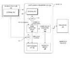
- FIG. 1is a functional block diagram illustrating a fingerprinting infrastructure 100 for authenticating bindings of hardware devices and physical structures and detecting device tampering and subversion by substitution, in accordance with an embodiment of the invention.
- the illustrated embodiment of infrastructure 100includes a hardware device 105 and a physical structure 122 to be authenticated, a challenger 110 interested in authenticating the binding of hardware device 105 and physical structure 122 , and a binding fingerprint list 115 maintained or certified by a certification authority 120 .
- the illustrated embodiment of hardware device 105includes a hardware platform 125 , primary circuitry (or function logic) 130 of the device, a cryptographic fingerprint unit 135 including an internal.
- the RFID tag 150is part of the hardware device 105 .
- the hardware platform itselfcan be an RFID tag.
- the RFID's ICcan be bound to the RFID's packaging.
- Cryptographic fingerprint unit 135may be implemented entirely within hardware or partially using hardware and partially using software/firmware.
- the internal PUF circuit 140which may be implemented using any PUF circuit having suitably small intra-device variation and sufficiently large inter-device variation, including but not limited to PUF circuits 900 , 1000 , 1100 , 1200 , along with primary circuitry 130 are both integrated into hardware platform 125 .
- hardware device 105is a semiconductor based integrated circuit (“IC”)
- the internal PUF circuit 140may be integrated into the semiconductor die including circuitry 130 .
- other components of cryptographic fingerprint unit 135may also be integrated into hardware platform 125 of hardware device 105 .
- Hardware device 105may represent any device of which hardware authentication during the deployment phase of its lifecycle is desired.
- hardware device 105may represent a CPU, a microcontroller, video card, or virtually any hardware device, which may or may not include software/firmware code.
- Hardware platform 125may include a semiconductor die of an application specific IC (“ASIC”) or general purpose IC (e.g., CPU), a field programmable gate array (“FPGA”), a printed circuit board (“PCB”), or otherwise. It should be appreciated that hardware platform 125 may include memory units for storing executable code (e.g. software or firmware) for operating primary circuitry 130 and/or portions of cryptographic fingerprint unit 135 .
- executable codee.g. software or firmware
- RFID tag 150may be incorporated into hardware device 105 for the purpose of identification and tracking using radio waves. An RFID tag reader from several meters away and beyond the line of sight can read RFID tag 150 .
- RFID tag 150may include an integrated circuit for storing and processing information, modulating and demodulating a RF signal, and an antenna for receiving and transmitting the signal.
- RFID tag 150can be implemented partially or fully in device circuitry 130 .
- hardware device 105may be a device for monitoring and tracking power consumption in a commercial or residential structure. The binding of the physical structure and hardware device 105 can detect device tampering and subversion, while RFID tag 150 can provide the ability for a person to authenticate the binding, as well as read the power consumption values.
- hardware device 125 , physical structure 122 , and/or RFID tag 150can be used in other applications.
- I/O ports 145External communication with cryptographic fingerprint unit 135 is conducted through I/O ports 145 .
- I/O ports 145may include existing industry standard test ports, such as a Joint Test Action Group (“JTAG”) test access port (“TAP”).
- JTAGJoint Test Action Group
- TAPtest access port
- external communicationsmay be multiplexed over standard data ports or other types of test ports.
- the illustrated embodiment of physical structure 122includes an external PUF circuit 142 .
- the external PUF circuit 142generates a unique external PUF value.
- cryptographic fingerprint unit 135is configured to measure the internal PUF value and the external PUF value located on physical structure 122 .
- the external. PUF valueis measured by circuitry disposed on or within physical structure 122 and sent to hardware device 105 , as described herein. Unlike the internal PUF value that remains internal to hardware device 105 and is not transmitted externally, the external PUF value is external to hardware device 105 and is transmitted to hardware device 105 for binding and authenticating purposes. For example, as described with respect to FIG.
- the external PUF valuecan be measured by a second integrated circuit and transmitted to cryptographic fingerprint unit 135 via I/O ports 145 .
- external PUF circuit 142can be integrated or packaged with the integrated circuit, and may be any PUF circuit having suitably small intra-device variation and sufficiently large inter-device variation, including but not limited to PUF circuits 900 , 1000 , 1100 , 1200 .
- the external PUFis an analog PUF, such as a coating PUF (illustrated in FIG. 13 ) disposed on or within physical structure 122 .
- the analog PUFwhich is located on or within physical structure 122 outputs the external PUF value, which is combined with the internal PUF value to generate a binding PUF value, as described in more detail below.
- Physical structure 122may be strain-sensitive tape, a fastener (e.g., a bolt, a buckle, a clamp, a clasp, a clip, a hasp, a hook, a latch, a snap, a screw, etc), a dielectric material having printed conductive wires or traces, a polymer having embedded conductive particles, a coating having embedded dielectric particles, a semiconductor die, a flexible substrate, or the like.
- physical structure 122includes an RFID tag, similar to RFID tag 150 described above.
- the RFID tagcould be embedded in physical structure 122 .
- the RFID tagcan wirelessly transmit a RF signal to cryptographic fingerprint unit 135 with the external PUF value.
- the RFID tag's integrated circuitmay measure the external PUF value, and send the external PUF value to cryptographic fingerprint unit 135 for binding and for authentication.
- the signalmay include the external PUF value itself or a value derived from the external PUF value, such as an encrypted value of the external PUF value.
- cryptographic fingerprint unit 135if cryptographic fingerprint unit 135 does not detect the RFID tag or if a different value is detected for the RFID tag, cryptographic fingerprint unit 135 will know that the physical structure has been tampered with or substituted, and the authentication will fail.
- the physical structuremay include other circuitry than an RFID tag to measure and transmit the external PUF value to cryptographic fingerprint unit 135 for binding and authenticating physical structure 122 and hardware device 105 .
- FIG. 2is a functional block diagram illustrating a cryptographic fingerprint unit 235 for authenticating a binding between hardware device 105 and physical structure 122 , in accordance with an embodiment of the invention.
- the depicted cryptographic fingerprint unit 235includes the internal PUF circuit disposed in or on hardware device 105 , binding logic 210 (e.g., depicted XOR operation), noise reduction circuit 220 , a cryptographic unit 230 , a symmetric key generation unit 240 , and encrypted memory 250 .
- the internal PUF circuit 140outputs the internal. PUF value.
- Binding logic 210receives the internal PUF value and an external PUF value.
- binding logic 210receives the external PUF value from external PUF circuit 142 of physical structure 122 and generates a binding PUF value using the internal and external PUF values.
- cryptographic fingerprint unit 235measures the internal PUF value and the external PUF value and inputs the values into binding logic 210 .
- binding logic 210uses an XOR function to combine the two values.
- other logic operationsmay be used, such as XNOR, NAND, AND, OR, a concatenation operation, or any logic operation that does not amplify the noise. Addition and subtractive operations may not be ideal because small change in the input can lead to large changes in output.
- noise reduction circuit 220is interposed between binding logic 210 and cryptographic unit 230 to convert the noisy binding PUF value to a filtered PUF seed that is stable and repeatable.
- noise reduction circuit 220operates to remove the intra-device uncertainty in the noisy binding PUF value.
- noise reduction circuit 220is implemented as a fuzzy extractor, which uses error code correcting (“ECC”) techniques to remove undesirable variability. Operation of a fuzzy extractor implementation of noise reduction circuit 220 is discussed in detail in connection with FIGS. 7 and 8 below.
- the cryptographic unit 230is coupled to receive the filtered binding seed value, which is based on the binding PUF value.
- the cryptographic unit 230uses the binding seed value to generate a cryptographic key.
- the cryptographic keyis a public key of an asymmetric key pair that allows challenger 110 (e.g. authenticating entity) to authenticate the binding of hardware device 105 and physical structure 122 using encryption and decryption.
- the cryptographic unit 230uses the binding seed value to generate other cryptographic keys for other authentication techniques, for example, those that don't require encryption and decryption (e.g., the Schnorr identification protocol).
- cryptographic unit 230includes a key generator and a decryptor, as illustrated and described in more detail with respect to FIG. 6 ).
- the key generatorreceives the binding seed value from the noise reduction circuit 220 , and generates the private key S and the public key P based on the binding PUF value.
- the decryptorreceives an authentication challenge, posed to hardware device 105 and encrypted with the public key P, and outputs a response to the authentication challenge decrypted with the private key S.
- the cryptographic unit 230may operate in an initial enrollment phase and subsequent authentication phases as described below.
- the private keyis never transmitted externally to the hardware device 105 , and is not stored or retained any longer than required to decrypt the authentication challenge. Each time the private key is needed by the hardware device 105 , the private key is regenerated using the internal and external PUF values, and then subsequently deleted or erased after use.
- cryptographic fingerprint unit 235measures the internal PUF (e.g., integrated PUF) and an analog PUF (e.g., coating PUF) located on physical structure 122 .
- the PUF responsesare combined using binding logic 210 , illustrated in FIG. 2 as an XOR operation, and input to noise reduction circuit 220 (e.g., a fuzzy extractor), which runs its enrollment procedure to generate helper data W and the filtered seed value (e.g., a unique identifier I).
- noise reduction circuit 220e.g., a fuzzy extractor
- Cryptographic fingerprint unit 235stores the helper data W publicly (e.g., stored publicly on the IC and/or external to the IC), and inputs I (the filtered seed value) to cryptographic unit 230 .
- the cryptographic unit 230uses I to generate a public key P that is emitted from hardware device 105 , and stored in a binding fingerprint list 115 , which is signed by certificate authority 120 , for example. After key generation, device circuitry 130 (e.g., IC) then clears its internal registers so that the PUF responses, binding PUF value, and any values stored in noise reduction circuit 230 and cryptographic unit 230 are erased.
- device circuitry 130e.g., IC
- challenger 110selects or generates a test value or test random value, c, as a secret phrase challenge to authenticate the binding of hardware device 105 and physical structure 122 , and encrypts c with the public key P belonging to the binding combination of hardware device 105 and physical structure 122 .
- Challenger 110sends a challenge P(c) to cryptographic fingerprint unit 235 .
- Cryptographic fingerprint unit 235measures its own internal PUF and the physical structure's external PUF, and binding logic 210 combines them to generate the binding PUF value.
- the helper data Wstored publicly on the IC, external to the IC, sent by the authenticating entity, or otherwise
- the binding seed valuee.g., identifier I from the noisy PUF measurements.
- Cryptographic fingerprint unit 235returns c to challenger 110 ,
- binding logic 210is coupled between the noise reduction circuit 220 and cryptographic unit 230 (illustrated in FIG. 2 with dashed lines).
- noise reduction circuit 230receives the noisy internal PUF value from internal. PUF circuit 140 , and converts the noisy internal PUF value to a filtered PUF seed that is stable and repeatable (e.g., corrects for intra-device variation).
- Binding logic 210receives the filtered PUF seed and combines it with the external PUF value to create the binding PUF value that is used to seed cryptographic unit 230 for the key generation. This binding PUF value can also be used to seed a symmetric key generation unit 240 as described below.
- this embodimentmay give the wrong keys if there is any noise in the external PUF value, since the internal PUF is error corrected, but the external PUF is not.
- other configurationsmay be used to create the binding PUF value from the internal and external PUF values.
- FIG. 2also depicts an optional symmetric key generation unit 240 and an optional encrypted memory 250 (illustrated with dashed lines).
- cryptographic fingerprint unit 235can use the binding seed value (e.g., the identifier I) to generate a symmetric key that is used by cryptographic fingerprint unit 235 for encryption and decryption of the contents of an internal memory to secure the internal memory as encrypted memory 250 .
- Encrypted memory 250may be used to store data associated with hardware device 105 and physical structure 122 .
- Encrypted memory 250may also be used to store data about other items, such as a container used to transport items that used the binding of hardware device 105 and physical structure 122 (e.g., to prevent tampering, subversion, or proliferation), the items or contents being transported in the container, and/or the like.
- a containerused to transport items that used the binding of hardware device 105 and physical structure 122 (e.g., to prevent tampering, subversion, or proliferation), the items or contents being transported in the container, and/or the like.
- FIG. 2may be used in applications, such as in a pharmaceutical supply chain, which may not require the highest levels of security.
- the external PUF valueis measured by cryptographic fingerprint unit 235 or sent to cryptographic fingerprint unit 235 over an unsecure communication channel.
- other configurationsmay be used to communicate the external PUF value to hardware device 105 securely.
- FIG. 3depicts a modification to the fingerprinting infrastructure of FIGS. 1 and 2 that may be more suitable for applications, such as non-proliferation, that require higher levels of security.
- FIG. 3may prevent spoofing of the physical structure's PUF by placing an IC 310 , such as those used on smart cards to cover at least a portion of the physical structure's PUF, for example.
- Cryptographic fingerprint unit 335is similar to cryptographic fingerprint unit 235 described above, except where specifically noted.
- the enrollment and authentication proceduresare the same as described above with respect to FIG. 2 , with the exception that the physical structure's PUF can be communicated to cryptographic fingerprint unit 335 (e.g., IC of the hardware device) over a secure, encrypted channel 320 using encryption logic 315 on IC 310 and decryption logic 325 of hardware device 105 (illustrated in FIG. 3 as part of cryptographic fingerprint unit 335 ).
- Encryption logic 315is configured to encrypt the external PUF value before sending the external PUF value to cryptographic fingerprint unit 335 .
- the decryption logicis configured to decrypt the external PUF value, which was encrypted by encryption logic 315 .
- secure communication channel 320could be created with a mutual authentication protocol based on additional PUF values used to bind two integrated circuits together.
- IC 310 and cryptographic fingerprint unit 335may use other encryption techniques to secure communication channel 320 , such as symmetric key encryption, using a symmetric key agreed upon by the devices (e.g., IC 310 and hardware device 105 ) during enrollment and stored securely by the devices, or by some other means.
- IC 310can measure the external PUF value and send the external PUF value to cryptographic fingerprint unit 335 .
- IC 310covers at least a part of external PUF circuit 142 .
- IC 310can measure physical structure's PUF 142 , such as, for example, from underneath IC 310 . Any attempt to remove IC 310 to gain access to physical structure's PUF 142 would alter external PUF 142 and indicate tampering during authentication.
- the external PUF circuitis a coating PUF (e.g., coating PUF 1300 depicted in FIG. 13 ) disposed to cover at least a portion of IC 310 .
- the coating PUFmay include a coating, which is doped with dielectric particles having random sizes and shapes.
- the dielectric particleshave a relative dielectric constant that differs from the dielectric constant of the coating.
- IC 310measures the coating PUF and sends the external PUF value to cryptographic fingerprint unit 335 . In another embodiment, IC 310 sends the external PUF over an unencrypted channel.
- binding logic 210 of cryptographic fingerprint unit 335may be interposed between internal PUF 140 and noise reduction circuit 220 (illustrated in FIG. 3 ), or between noise reduction circuit 220 and cryptographic unit 230 (not illustrated in FIG. 3 ).
- other configurationsmay be used to create the binding PUF value from the internal and external PUF values.
- IC 310can include a cryptographic system that includes encryption logic 315 , as well as a noise reduction circuit, similar to noise reduction circuit 220 of cryptographic fingerprint unit 335 .
- the noise reduction circuitconverts the noisy external PUF value to a filtered PUF seed that is stable and repeatable.
- the noise reduction circuitcould be used to remove uncertainty in the noisy external PUF value before encrypting and sending the external PUF value to cryptographic fingerprint unit 235 .
- IC 310includes the noise reduction circuit without encryption logic 315 and sends the filtered external PUF value over an unsecure communication channel.
- external PUF circuit 142which may be implemented using any PUF circuit having suitably small intra-device variation and sufficiently large inter-device variation, including but not limited to PUF circuits 900 , 1000 , 1100 , 1200 , along with primary circuitry 130 are both integrated into IC 310 .
- external PUF circuit 142may be integrated into a semiconductor die of IC 310 .
- FIG. 4is a flow chart illustrating process 400 for uniquely fingerprinting a binding of a hardware device and a physical structure, in accordance with an embodiment of the invention.
- the order in which some or all of the process blocks appear in process 400should not be deemed limiting. Rather, one of ordinary skill in the art having the benefit of the present disclosure will understand that some of the process blocks may be executed in a variety of orders not illustrated.
- internal PUF circuit 140generates a unique internal PUF value that is measured by cryptographic fingerprint unit 135 (or 235 or 235 ).
- the internal PUF valueremains internal to hardware device 105 and is not transmitted externally.
- the internal PUF valueis generated in real-time each time it is need and is not stored for future use internally.
- binding logic 210receives the external PUF value from physical structure 122 .
- the external PUF valuemay be generated in real-time each time it is needed and is not stored for future use by physical structure 122 or hardware device 105 . Since the external PUF value is generated externally to cryptographic fingerprint unit 135 , the external PUF value may be encrypted using encryption logic on an IC disposed on physical structure 122 as described above.
- cryptographic fingerprint unit 335decrypts the encrypted external PUF value before inputting the external PUF into binding logic 210 .
- binding logic 210generates a binding PUF value from the internal PUF value and the external PUF value.
- the binding PUF valueis used as a binding seed value to a cryptographic function.
- the cryptographic functionmay be the creation of a public-private key pair where the binding PUF value is the binding seed value for the key generator.
- Hardware device 105can delete all instances of the binding PUF value and the binding seed value within hardware device 105 after seeding the cryptographic function.
- cryptographic fingerprint unit 135generates the public key of a public-private key pair.
- the public-private key pairis generated according to the RSA (Rivest, Shamir and Adleman) cryptographic algorithm using a binding seed value generated from the combined internal and external PUF values.
- a process block 420the public key from the public-private key pair is output from device 125 via I/O ports 145 . If a standard unique, binding identifier (“ID”) is to be used (decision block 421 ), then process 400 continues to a process block 425 .
- the public keyis stored into a binding fingerprint list 115 and indexed to ID referencing device 125 .
- the combination of the public key and IDoperate as a sort of cryptographic hardware fingerprint that is uniquely associated with the particular hardware instance of hardware device 105 .
- the binding IDmay be a combination of a manufacturing serial number, a globally unique identifier (“GUID”), or other unique identifier associated with hardware device 105 , and a number associated with physical structure 122 .
- the binding IDmay be a random generated value or a pseudo-random generated value.
- Binding fingerprint list 115may be populated by a manufacturer of hardware device 105 prior to hardware device 105 being shipped to customers as a means of tracking and authenticating part numbers.
- Binding fingerprint list 115may subsequently be accessed by a customer, an OEM manufacturer incorporating hardware device 105 into a larger system, an end-user, or a third party interacting with hardware device 105 (either directly or remotely over a network) wishing to authenticate hardware device 105 (discussed in connection with FIG. 5 ). As an added security measure, binding fingerprint list 115 may be signed and maintained by a trusted third party, such as a certification authority 120 of a public key infrastructure (process block 430 ).
- a trusted third partysuch as a certification authority 120 of a public key infrastructure
- cryptographic fingerprint unit 135generates the ID as a randomized value.
- the IDcan be generated based on a portion of the binding PUF value output from PUF 140 .
- a second ID PUFmay be included within cryptographic fingerprint unit 135 for generating a randomized ID.
- the ID PUFcan be “reprogrammed” using PUF perturbation devices 625 (discussed below in connection with FIG. 6 ), thus causing the ID PUF to generate a new, hopefully unique, ID value.
- PUF perturbation devices 625can be reprogrammed multiple times during the enrollment procedure until a unique ID is obtained (statistically it is highly unlikely that perturbation devices 625 would have to be adjusted multiple times to achieve a unique output binding PUF value).
- the above combination of elements and proceduresforms a method of enrolling the binding of the hardware component and the physical structure, thus forming a deterrent against insertion of a subversion or substitution of a subverted component by an adversary who wishes to avoid attribution upon subsequent discovery of the subversion or against device tampering of content of a container, for example.
- FIG. 5is a flow chart illustrating a process 500 for authenticating a binding of a hardware device and a physical structure during the deployment phase of its lifecycle using a cryptographic challenge/response and a binding fingerprint, in accordance with an embodiment of the invention.
- the order in which some or all of the process blocks appear in process 500should not be deemed limiting. Rather, one of ordinary skill in the art having the benefit of the present disclosure will understand that some of the process blocks may be executed in a variety of orders not illustrated.
- challenger 110retrieves the binding ID associated with binding of hardware device 105 and physical structure 122 .
- challenger 110retrieves the binding ID from hardware device 105 either manually or via an electronic query.
- the binding IDmay be a serial number physically displayed on the part (e.g., sticker, engraving, printed, etc.) or it may be electronically stored within hardware device 105 (e.g., within non-volatile memory).
- challenger 110uses the binding ID to access the associated public key from binding fingerprint list 115 .
- the binding IDis used to retrieve a signed certificate from certification authority 120 , which includes the public key.
- the listitself may also be authenticated with reference to its certification signature to ensure the list has not been compromised (process block 515 ). If the signature is validly authenticated, then challenger 110 can retrieve the public key with assurances that it has not been tampered with (process block 520 ).
- challenger 110generates a test value or test message for submission to cryptographic fingerprint unit 135 as a sort of secret phrase challenge.
- the test valuecan be a numeric value, an alphanumeric phrase, or otherwise.
- challenger 110encrypts the test value using the private key obtained in process block 520 .
- the encrypted test valueis submitted to cryptographic fingerprint unit 135 as a sort of cryptographic challenge.
- binding of hardware device 105 and physical structure 122is the same as when enrolled, representing the original binding or a non-tampered binding; then hardware device 105 will be able to regenerate the binding PUF value used to seed the key generator that created the original public-private key pair. Thus, binding of hardware device 105 and physical structure 122 is the only binding that will be able to regenerate the original private key to decrypt the encrypted test value and respond to the challenged with the decrypted test value.
- binding logic 210receives the external PUF value from physical structure 122 .
- binding logic 210generates the binding PUF from the internal and external PUF values, and seeds the cryptographic function with the binding PUF value (process block 546 ).
- the key generatoruses the binding PUF value to generate the private key.
- the binding of hardware device 105 and physical structure 122is contemporaneously being retested at the time of the challenge.
- cryptographic fingerprint unit 135decrypts the test value (process block 555 ) and responds to challenger 110 with the decrypted test value (process block 560 ). Finally, in a process block 565 , challenger 110 compares the test value received in the response from hardware device 105 to the original test value it has selected and encrypted. If the two match, challenger 110 can be confident that the binding of hardware device 105 and physical structure 122 has not be tampered with, or subverted by substituting parts, since the only device in possession of the private key necessary to decrypt the test value would be hardware device 105 being challenged.
- private keytransmitted external to hardware device 105 , and furthermore in some embodiments private key is not stored or retained any longer than required to respond to a given challenge.
- the private keyis regenerated using the internal and external PUF values.
- FIG. 6is a functional block diagram illustrating a cryptographic fingerprint unit 600 , in accordance with an embodiment of the invention.
- Cryptographic fingerprint unit 600is one possible implementation of cryptographic fingerprint unit 135 illustrated in FIG. 1 , cryptographic fingerprint unit 235 illustrated in FIG. 2 , and cryptographic fingerprint unit 335 illustrated in FIG. 3 .
- the illustrated embodiment of cryptographic fingerprint unit 600includes a PUF circuit 605 , binding logic 210 , a noise reduction circuit 610 , a key generator 615 , a decryptor 620 , PUF perturbation devices 625 , and a control unit 630 .
- the illustrated embodiment of noise reduction circuit 610includes a data store 611 , a seed generation mode 612 , and a seed recovery mode 613 .
- Control unit 630may receive inputs and generate outputs to be coupled to the components of fingerprint unit 600 to choreograph their operation.
- Control unit 630may be implemented as software/firmware instructions executing on a microcontroller, an ASIC, a state machine, or otherwise. In some embodiments, control unit 630 need not control all of the components of fingerprint unit 600 .
- PUF circuit 605is implemented using a cross-coupled type PUF (illustrated in FIG. 11 )
- control unit 630may not provide any control signaling to PUF circuit 605 or may simply include an enable signal to enable PUF circuit 605 .
- control unit 630may receive the SEL bits as the INPUT to configure PUF circuit 605 .
- the SEL bitsmay be part of the cryptographic challenge posed by challenger 110 .
- PUF perturbation devices 625are programmable devices that can be used to increase the variability of PUF circuit 605 by affecting the delay paths within PUF circuit 605 .
- PUF perturbation devices 625may be programmable by the end user to facilitate user customization and user control over the variability and output of PUF circuit 605 .
- PUF perturbation devices 625are
- PUF circuit 605outputs an internal PUF value, which may be an inherently noisy value in some designs due to thermal variations, etc.
- Binding logic 210receives the internal PUF value and an external PUF value from the external PUF circuit 607 as described above (e.g., measured by cryptographic fingerprint unit 135 , 235 or 335 , or measured and sent by an IC 310 to hardware device 105 ). Binding logic 210 combines the PUF value and the external PUF value, which may or may not be noisy, to create the binding PUF value (noisy).
- binding logic 210can feed the binding PUF value (noisy) into noise reduction circuit 610 , which is interposed between the key generator 615 and binding logic 210 to convert the noisy binding PUF value to a filtered binding PUF seed that is stable and repeatable. While it is desirable for a given PUF circuit 605 to output different, random values between different physical devices, it is not desirable for a given PUF circuit 605 of a single instance of hardware device 105 to output different values over its lifecycle (unless PUF perturbation devices 625 have been reprogrammed by the end user as part of a deliberate re-fingerprinting of hardware device 105 ).
- noise reduction circuit 610operates to remove the uncertainty in the noisy binding PUF value, which may be caused by noisy PUF values from either or both of the internal and external PUF circuits.
- noise reduction circuit 610is implemented as a fuzzy extractor, which uses ECC techniques to remove undesirable variability. Operation of a fuzzy extractor implementation of noise reduction circuit 610 is discussed in detail in connection with FIGS. 7 and 8 below.
- Key generator 615is coupled to receive a binding seed value, which is based on the binding PUF value combined from the internal and external PUF values from PUF circuit 605 and external PUF circuit 607 .
- Key generator 615uses the binding seed value to seed its encryption engine and generate a unique public-private key pair.
- the public-private key pairis generated according to the RSA cryptographic algorithm.
- the private keyis also kept internal to cryptographic fingerprint unit 135 ( 235 or 335 ) and never exported externally from hardware device 105 .
- the public keyis exported from hardware device 105 along with a binding ID to enroll the binding fingerprint with binding fingerprint list 115 .
- Cryptographic fingerprint unit 135( 235 or 335 ) as the sole holder of the private key, is the only entity capable of decrypting a message encrypted using the corresponding public key so long as its binding with the physical structure is maintained.
- challenger 110presents its cryptographic challenge in the form of an encrypted message to hardware device 105 .
- Decryptor 620receives the challenge and uses the private key to decrypt the message and generate the response.
- noise reduction circuit 610includes at least two modes of operation: seed generation mode 612 and a seed recovery mode 613 .
- Control unit 630places noise reduction circuit 610 into the seed generation mode 612 when creating a new cryptographic binding fingerprint for the binding of hardware device 105 and physical structure 122 , while control unit 630 places noise reduction circuit 610 into the seed recovery mode 613 during a cryptographic authentication event.
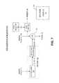
- FIG. 7is a dataflow diagram illustrating seed generation mode 612 of noise reduction circuit 610 during creation of a binding fingerprint, in accordance with an embodiment of the invention.
- noise reduction circuit 610is configured to include an encoder 705 , a logic unit 710 , a hash unit 715 , a hash selector 717 , and data store 611 .
- the illustrated embodiment of encoder 705includes an ECC encoder 720 and a repetition encoder 725 .
- Noise reduction circuit 610may be configured to operate in the seed generation mode 612 by enabling hardware components to implement the dataflow illustrated in FIG. 7 , by loading/executing software/firmware modules to implement the dataflow illustrated in FIG. 7 , by reconfiguring interconnections between the ECC encoder 720 , repetition encoder 725 , logic unit 710 , and hash unit 715 to form the dataflow illustrated in FIG. 7 , some combination thereof, or otherwise.
- Each component illustrated in FIG. 7may be implemented entirely in hardware, entirely in software, or a combination of both.
- noise reduction in the noisy binding PUF valueis achieved via application of error correction techniques to the binding PUF value so that future bit errors in the binding PUF value can be identified and corrected to generate a reliable, consistent, and less noisy seed value.
- ECC techniquesmay be applied (e.g., Reed-Solomon, repetition, Hamming, low-density parity-check (LDPC), etc); however, in one embodiment, ECC encoder 720 is implemented using a BCH (Bose, Chaudhuri, Hocquenghem) encoder to generate an error correcting codeword Cs. To ensure security and prevent an adversary from reverse generating the binding seed value, the codeword Cs should be selected randomly. Accordingly, in one embodiment, a first portion of the binding PUF value itself is used to generate the codeword Cs during the seed generation mode 612 .
- binding logic 210is enabled, and the output value of PUF circuit 605 and external PUF circuit 607 are measured and combined to form the binding PUF value.
- a first portion of the binding PUF value binding PUF[178 . . . 0]is provided to encoder 705 while a second portion of the binding PUF value binding PUF[2473 . . . 179] is provided to logic unit 710 and hash unit 715 .
- ECC encoder 720uses the first portion binding PUF[78 . . . 0] to generate the codeword Cs[254 . . . 0].
- the codewordis expanded using repetition encoder 725 to generate codeword Cs[2294 . . . 0].
- FIG. 7illustrates the use of a 255-bit codeword and a 9 ⁇ repetition encoder
- longer or shorter codewords and higher or lower repetition encodersmay be used according to the level of noise in the binding PUF value.
- one technique for improving error correcting abilityis to concatenate codes, such as by a concatenation of a strong code (such as BCH) and weak code (such as repetition) as described in connection with FIG. 7 , but other techniques may be used.
- FIG. 7illustrates a 2474-bit binding PUF value, longer or shorter binding PUF values may be used according to the desired strength of security.
- Repetition encoder 725may be replaced by other types of encoders as well.
- Logic unit 710combines the second portion of the binding PUF value binding PUF[2473 . . . 179] with the codeword Cs[2294 . . . 0] to generate helper data W 1 [2294 . . . 0].
- logic unit 710uses an XOR function to combine the two values, though other logic functions may be implemented (e.g., XNOR).
- the helper data W 1 [2294 . . . 0]is a value, which is used during the seed recovery mode 613 to regenerate the seed value SEED[127 . . .
- Hash unit 715hashes the second portion binding PUF[2473 . . . 179] to generate the fixed length seed value SEED[127 . . . 0].
- the hash unit 715performs a function known as “privacy amplification” or “entropy amplification” since the entropy per bit in the binding PUF[2473 . . . 179] will be less than one.
- the width of the binding PUF value input into hash unit 715 and the width of the seed value output from hash unit 715are engineered to compensate for average deficiency in entropy rate in the inter-device variability of the PUF measurements.
- the particular hash algorithmis also selected from a large set of hash algorithms, in which case, helper data W 2 indicating the particular hash algorithm selected is also stored into data store 611 .
- hash selector 717generates W 2 to implement a randomized selection of the hash algorithm.
- hash selector 717uses a portion of the binding PUF value to randomly select a particular hash algorithm from a liner feedback shift register (LFSR) hash.
- LFSRliner feedback shift register
- hash selector 717includes an LFSR hash coupled to receive a portion of the binding PUF value. The output of the LFSR hash is then coupled into an irreducible polynomial generator, which outputs the W 2 value for selecting the hash algorithm.
- hash selector 717includes a random number generator coupled to an irreducible polynomial generator to generate W 2 .
- FIG. 8is a dataflow diagram illustrating seed recovery mode 613 of noise reduction circuit 610 during authentication of a binding fingerprint, in accordance with an embodiment of the invention.
- noise reduction circuit 610is configured to include two logic units 710 , a decoder 805 , encoder 705 , and hash unit 715 .
- decoder 805includes a repetition decoder 810 and an ECC decoder 815 .
- Noise reduction circuit 610may be configured to operate in the seed recovery mode 613 by enabling hardware components to implement the dataflow illustrated in FIG. 8 .
- the dataflow illustrated in FIG. 8may be achieved by loading/executing software/firmware modules, by reconfiguring interconnections between the components, some combination thereof, or otherwise.
- Each component illustrated in FIG. 8may be implemented entirely in hardware, entirely in software, or a combination of both.
- binding logic 210is enabled and receives the PUF values from PUF circuit 605 and external PUF circuit 607 . Since the PUF values may be noisy values, the measured values may not be identical to the original PUF values measured during seed generation mode 612 , and thus, the binding PUF value may not be identical to the original binding PUF value generated during seed generation mode 612 . Accordingly, the subsequently measured binding PUF value is labeled as BINDING PUF′ and the error correcting codeword generated based on BINDING PUF′ is labeled as Cs′ in FIG. 8 .
- a first portion of the binding PUF′ value BINDING PUF′[2473 . . . 179]is combined by logic unit 710 with the helper data W 1 [2294 . . . 0] to generate the codeword Cs′[2294 . . . 0]. If BINDING PUF′ happens to be identical to BINDING PUF, then Cs′ would be equal to Cs. However, if BINDING PUF′ is a noisy value with at least one flipped bit, then BINDING PUF′ does not equal BINDING PUF and error correcting techniques will remove the errors and regenerate the original binding PUF value BINDING PUF[2473 . . . 179] and the original seed value SEED[127 . . . 0].
- Repetition decoder 810decodes Cs′[2294 . . . 0] down to Cs′[254 . . . 0], which is input into ECC decoder 815 to generate the original BINDING PUF[178 . . . 0]. With the original first portion of the binding PUF value in hand, BINDING PUF[178 . . . 0] is inserted back into encoder 705 to generate the original codeword Cs[2294 . . . 0]. With Cs[2294 . . . 0] in hand, logic unit 710 is once again used to combine Cs[2294 . . . 0] with helper data W 1 [2294 . . .
- hash unit 715uses the second portion of the binding PUF value to recreate the original seed value SEED[127 . . . 0]. If a fixed hash algorithm is not used, then helper data W 2 is retrieved from data store 611 to select the appropriate hash algorithm.
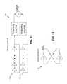
- FIG. 9Ais a logic circuit diagram of an arbiter PUF 900 .
- Each stage of arbiter PUF 900is a switch circuit 905 , illustrated in FIG. 9B .
- FIG. 9Billustrates that switch circuit 905 includes a pair of two input multiplexers 910 with a shared select signal (SEL).
- SELshared select signal
- SELshared select signal
- Arbiter PUF 900chains n switch circuits 905 together.
- an arbiter(e.g., latch 915 ) determines the output of the circuit; if the D input arrives first the output is ‘0’ and if the E input arrives first the output is ‘1’.
- Arbiter PUF 900accepts an n-hit input SEL and produces as output a single bit. This generates a challenge-response pair wherein the challenge is the input, or sequence of inputs, and the response is the output or sequence of outputs. As such, this PUF has an intrinsic challenge-response capability. The PUF output is the response to a particular challenge. To achieve a k-hit response, one may provide k different inputs to a single arbiter PUF 900 , evaluate k instantiations of arbiter PUF 900 , or some combination thereof.
- FIG. 10is a logic circuit diagram of a ring oscillator PUF 1000 .
- Ring oscillator PUF 1000exploits variations in the resonance frequencies of a set of identical ring oscillators 1005 and 1010 .
- To produce an output bitthe resonance frequencies of ring oscillators 1005 and 1010 are compared and the output bit is determined by which oscillator is fastest.
- a k bit sequenceis produced by making k comparisons between multiple different ring oscillators; however, one should be careful to choose independent, uncorrelated comparisons.
- ring oscillator PUF 1000When compared to arbiter PUF 900 , disadvantages of ring oscillator PUF 1000 include area, speed, and power dissipation. However, ring oscillator PUF 1000 is likely easier to implement since it does not require routing two long, almost identical paths across an ASIC or FPGA, as is the case with arbiter PUF 900 .
- FIG. 11is a logic circuit diagram of a cross-coupled PUF 1100 .
- Cross-coupled PUF 1100uses a positive feedback loop to store a bit. Without applying any external stimulus, the output of cross-coupled PUF 1100 will attain a stable output. The value of this output results from differences in interconnect delay and the voltage transfer characteristics of the inverters 1105 and 1110 .
- a k bit sequencecan be obtained from k cross-coupled inverter pairs.
- Other logic gates, such as NAND and NOR gatescan also be connected in a cross-coupled configuration to be used as a PUF.
- FIG. 12is a logic circuit diagram of a butterfly PUF 1200 .
- the illustrated embodiment of butterfly PUF 1200includes cross-coupled D latches 1205 and 1210 .
- the enable inputs (E) to the latchesare tied high so that the D input is always transferred to the Q output.
- Eenable inputs
- “in”is set to ‘0’, which causes the system to enter an unstable state. At this point, the positive feedback loop and differences in wire and latch propagation delays force the output to a stable value.
- k bitsare generated by implementing k butterfly PUFs within a given device.
- PUF circuitsin addition to those illustrated in FIGS. 9-12 , may be implemented in connection with embodiments of the invention as well.
- a variety of PUFsmay be suitable, as long as, a given PUF design has sufficiently small intra-device variation and sufficiently large inter-device variation given a desired level of security.
- intrinsic PUFswhich are created from a resource that already exists on an integrated, may be used.
- FPGAsthe startup values of SRAM and flip-flops may be leveraged.
- the primary advantage of intrinsic PUFsis that they are already present on the FPGA, and so only a readout circuit is needed to obtain the value of the PUF. In this sense, fewer FPGA resources are required to implement the function.
- SRAM and flip-flop states on FPGAsare commonly forced into a known state upon power up. As such, modification of the bit stream loaded into the FPGA may be necessary for readout.
- FIG. 13is a cross-sectional view of a coating type PUF.
- the coating type PUF 1300includes a substrate 1302 of a semiconductor die (e.g., silicon substrate), such as the substrate of the IC 310 of FIG. 3 .
- the IC 310can be covered with a coating 1308 (e.g., aluminophosphate), which is doped with random dielectric particles 1310 (e.g., TiO 2 , SrTiO 3 , BaTiO 3 ).
- the random dielectric particles 1310may be particles of random size and shape with a relative dielectric constant ⁇ r differing from the dielectric constant of the coating 1308 .
- the coating PUF 1300is made up of a combination of the coating 1308 with the dielectric material 1310 .
- an array of metal sensors 1304e.g. a comb structure
- the passivation layer 1306e.g. nitride passivation layer
- a challengemay correspond to a voltage of a certain frequency and amplitude applied to the sensors 1304 at a certain point of the sensor array.
- coating PUFshave the advantage of possessing a high degree of integration.
- the matrix containing the random particlescan be part of the opaque coating.
- the tamper-resistance coatingwhich protects the secrets present in the electronics (stored and during computation), itself serves as a carrier of (inherently tamper-resistant) secrets.
- Coating PUFsalso have the advantage that they can be easily turned into a controlled PUF (CPUF). The control electronics can simply be put underneath the coating. Probing the coating PUF from the outside gives insufficient information to the attacker.
- a computer-readable storage mediumincludes any mechanism that provides (e.g., stores) information in a form accessible by a machine (e.g., a computer, network device, personal digital assistant, manufacturing tool, any device with a set of one or more processors, etc.).
- a computer-readable storage mediumincludes recordable/non-recordable media (e.g., read only memory (ROM), random access memory (RAM), magnetic disk storage media, optical storage media, flash memory devices, etc.).
Landscapes
- Engineering & Computer Science (AREA)
- Computer Security & Cryptography (AREA)
- Software Systems (AREA)
- Theoretical Computer Science (AREA)
- Computer Hardware Design (AREA)
- Physics & Mathematics (AREA)
- General Engineering & Computer Science (AREA)
- General Physics & Mathematics (AREA)
- Computer Networks & Wireless Communication (AREA)
- Signal Processing (AREA)
- Semiconductor Integrated Circuits (AREA)
Abstract
Description
Claims (31)
Priority Applications (1)
| Application Number | Priority Date | Filing Date | Title |
|---|---|---|---|
| US12/908,324US8516269B1 (en) | 2010-07-28 | 2010-10-20 | Hardware device to physical structure binding and authentication |
Applications Claiming Priority (2)
| Application Number | Priority Date | Filing Date | Title |
|---|---|---|---|
| US12/844,860US8848905B1 (en) | 2010-07-28 | 2010-07-28 | Deterrence of device counterfeiting, cloning, and subversion by substitution using hardware fingerprinting |
| US12/908,324US8516269B1 (en) | 2010-07-28 | 2010-10-20 | Hardware device to physical structure binding and authentication |
Related Parent Applications (1)
| Application Number | Title | Priority Date | Filing Date |
|---|---|---|---|
| US12/844,860Continuation-In-PartUS8848905B1 (en) | 2010-07-28 | 2010-07-28 | Deterrence of device counterfeiting, cloning, and subversion by substitution using hardware fingerprinting |
Publications (1)
| Publication Number | Publication Date |
|---|---|
| US8516269B1true US8516269B1 (en) | 2013-08-20 |
Family
ID=48952286
Family Applications (1)
| Application Number | Title | Priority Date | Filing Date |
|---|---|---|---|
| US12/908,324Active2031-05-14US8516269B1 (en) | 2010-07-28 | 2010-10-20 | Hardware device to physical structure binding and authentication |
Country Status (1)
| Country | Link |
|---|---|
| US (1) | US8516269B1 (en) |
Cited By (121)
| Publication number | Priority date | Publication date | Assignee | Title |
|---|---|---|---|---|
| US20130094648A1 (en)* | 2011-10-12 | 2013-04-18 | Infineon Technologies Ag | Apparatus and Method for Producing a Bit Sequence |
| US20130141137A1 (en)* | 2011-06-01 | 2013-06-06 | ISC8 Inc. | Stacked Physically Uncloneable Function Sense and Respond Module |
| US20130234771A1 (en)* | 2010-11-24 | 2013-09-12 | Intrinsic Id B.V. | Physical unclonable function |
| US20130254636A1 (en)* | 2012-03-22 | 2013-09-26 | Purdue Research Foundation | System on chip and method for cryptography using a physically unclonable function |
| US20140053286A1 (en)* | 2011-04-14 | 2014-02-20 | Lockheed Martin Corporation | Dynamically reconfigurable 2d topology communication and verification scheme |
| US20140089685A1 (en)* | 2011-06-02 | 2014-03-27 | Mitsubishi Electric Corporation | Key information generation device and key information generation method |
| US20140123223A1 (en)* | 2012-07-18 | 2014-05-01 | Sypris Electronics, Llc | Resilient Device Authentication System |
| US20140145353A1 (en)* | 2012-11-26 | 2014-05-29 | Honeywell International Inc. | Tamper-resistant coating for an integrated circuit |
| US20140376717A1 (en)* | 2013-06-18 | 2014-12-25 | Nagravision S.A. | Method and unique cryptographic device with a physically unclonable function |
| US20150007337A1 (en)* | 2013-07-01 | 2015-01-01 | Christian Krutzik | Solid State Drive Physical Uncloneable Function Erase Verification Device and Method |
| US20150023495A1 (en)* | 2011-03-15 | 2015-01-22 | Irdeto B.V. | Change-tolerant method for generating identifier for collection of assets in computing environment using error-correction code scheme |
| US20150038118A1 (en)* | 2012-02-27 | 2015-02-05 | Morpho | Method for verifying the identity of a user of a communicating terminal and associated system |
| US20150046699A1 (en)* | 2012-03-19 | 2015-02-12 | Morpho | Method for generating public identity for authenticating an individual carrying an identification object |
| US20150095631A1 (en)* | 2013-09-30 | 2015-04-02 | Dell Products L.P. | Systems and methods for binding a removable cryptoprocessor to an information handling system |
| US9018972B1 (en)* | 2012-06-04 | 2015-04-28 | Sandia Corporation | Area-efficient physically unclonable function circuit architecture |
| US9048834B2 (en) | 2013-01-16 | 2015-06-02 | Intel Corporation | Grouping of physically unclonable functions |
| US20150242614A1 (en)* | 2014-02-25 | 2015-08-27 | Cambridge Silicon Radio Limited | Provisioning of security credentials |
| US9154310B1 (en)* | 2012-02-12 | 2015-10-06 | Sypris Electronics, Llc | Resilient device authentication system |
| US20150318994A1 (en)* | 2014-05-05 | 2015-11-05 | Sypris Electronics, Llc | System and device binding metadata with hardware intrinsic properties |
| US9202554B2 (en) | 2014-03-13 | 2015-12-01 | International Business Machines Corporation | Methods and circuits for generating physically unclonable function |
| US20150350072A1 (en)* | 2012-10-04 | 2015-12-03 | Siemens Aktiengesellschaft | Apparatus and Method for Transmitting Data |
| US9208355B1 (en)* | 2013-05-28 | 2015-12-08 | Sandia Corporation | Apparatus, system and method for providing cryptographic key information with physically unclonable function circuitry |
| US20160056953A1 (en)* | 2014-08-25 | 2016-02-25 | Kabushiki Kaisha Toshiba | Data generating device, communication device, mobile object, data generating method, and computer program product |
| US9390291B2 (en)* | 2012-12-29 | 2016-07-12 | Intel Corporation | Secure key derivation and cryptography logic for integrated circuits |
| US9444618B1 (en)* | 2013-04-22 | 2016-09-13 | Xilinx, Inc. | Defense against attacks on ring oscillator-based physically unclonable functions |
| JP2016531515A (en)* | 2013-08-23 | 2016-10-06 | クアルコム,インコーポレイテッド | Application of circuit delay based physical non-clonal function (PUF) to masking operation of memory based PUF to resist invasive clonal attack |
| US9501664B1 (en) | 2014-12-15 | 2016-11-22 | Sandia Corporation | Method, apparatus and system to compensate for drift by physically unclonable function circuitry |
| US20160344709A1 (en)* | 2015-05-19 | 2016-11-24 | Anvaya Solutions, Inc. | System and method for authenticating and enabling an electronic device in an electronic system |
| US20160359635A1 (en)* | 2011-03-11 | 2016-12-08 | Emsycon Gmbh | Tamper-protected hardware and method for using same |
| US20160359627A1 (en)* | 2014-01-10 | 2016-12-08 | Robert Bosch Gmbh | System and method for cryptographic key identification |
| US9554477B1 (en) | 2015-12-18 | 2017-01-24 | International Business Machines Corporation | Tamper-respondent assemblies with enclosure-to-board protection |
| US9560737B2 (en) | 2015-03-04 | 2017-01-31 | International Business Machines Corporation | Electronic package with heat transfer element(s) |
| US9555606B1 (en) | 2015-12-09 | 2017-01-31 | International Business Machines Corporation | Applying pressure to adhesive using CTE mismatch between components |
| US20170039364A1 (en)* | 2015-05-19 | 2017-02-09 | Anvaya Solutions, Inc. | System and method to cause an obfuscated non-functional device to transition to a starting functional state using a specified number of cycles |
| US9569601B2 (en)* | 2015-05-19 | 2017-02-14 | Anvaya Solutions, Inc. | System and method for authenticating and enabling functioning of a manufactured electronic device |
| US9578764B1 (en) | 2015-09-25 | 2017-02-21 | International Business Machines Corporation | Enclosure with inner tamper-respondent sensor(s) and physical security element(s) |
| US20170063821A1 (en)* | 2015-08-31 | 2017-03-02 | Mentor Graphics Corporation | Secure protocol for chip authentication |
| US9591776B1 (en) | 2015-09-25 | 2017-03-07 | International Business Machines Corporation | Enclosure with inner tamper-respondent sensor(s) |
| WO2017091133A1 (en)* | 2015-11-23 | 2017-06-01 | Authentico Technologies Ab | Method and system for secure storage of information |
| US9692538B2 (en) | 2014-02-25 | 2017-06-27 | Qualcomm Technologies International, Ltd. | Latency mitigation |
| US9759757B2 (en) | 2013-12-13 | 2017-09-12 | Battelle Memorial Institute | Electronic component classification |
| US9787670B2 (en)* | 2011-08-16 | 2017-10-10 | Ictk Co., Ltd | Apparatus and method for authentication between devices based on PUF over machine-to-machine communications |
| US20170346644A1 (en)* | 2016-05-24 | 2017-11-30 | Arizona Board Of Regents On Behalf Of Northern Arizona University | Systems implementing hierarchical levels of security |
| US9858776B1 (en) | 2016-06-28 | 2018-01-02 | International Business Machines Corporation | Tamper-respondent assembly with nonlinearity monitoring |
| US9881880B2 (en) | 2016-05-13 | 2018-01-30 | International Business Machines Corporation | Tamper-proof electronic packages with stressed glass component substrate(s) |
| US9887844B2 (en)* | 2013-12-27 | 2018-02-06 | Robert Bosch Gmbh | Method for safeguarding a system-on-a-chip |
| US9894749B2 (en) | 2015-09-25 | 2018-02-13 | International Business Machines Corporation | Tamper-respondent assemblies with bond protection |
| US9904811B2 (en) | 2016-04-27 | 2018-02-27 | International Business Machines Corporation | Tamper-proof electronic packages with two-phase dielectric fluid |
| US9913370B2 (en) | 2016-05-13 | 2018-03-06 | International Business Machines Corporation | Tamper-proof electronic packages formed with stressed glass |
| US9913389B2 (en) | 2015-12-01 | 2018-03-06 | International Business Corporation Corporation | Tamper-respondent assembly with vent structure |
| US9911012B2 (en) | 2015-09-25 | 2018-03-06 | International Business Machines Corporation | Overlapping, discrete tamper-respondent sensors |
| US9916744B2 (en) | 2016-02-25 | 2018-03-13 | International Business Machines Corporation | Multi-layer stack with embedded tamper-detect protection |
| US9924591B2 (en) | 2015-09-25 | 2018-03-20 | International Business Machines Corporation | Tamper-respondent assemblies |
| US9946858B2 (en) | 2014-05-05 | 2018-04-17 | Analog Devices, Inc. | Authentication system and device including physical unclonable function and threshold cryptography |
| US9978231B2 (en) | 2015-10-21 | 2018-05-22 | International Business Machines Corporation | Tamper-respondent assembly with protective wrap(s) over tamper-respondent sensor(s) |
| US9998445B2 (en) | 2013-11-10 | 2018-06-12 | Analog Devices, Inc. | Authentication system |
| US9999124B2 (en) | 2016-11-02 | 2018-06-12 | International Business Machines Corporation | Tamper-respondent assemblies with trace regions of increased susceptibility to breaking |
| US9996480B2 (en) | 2012-07-18 | 2018-06-12 | Analog Devices, Inc. | Resilient device authentication system with metadata binding |
| US10098235B2 (en) | 2015-09-25 | 2018-10-09 | International Business Machines Corporation | Tamper-respondent assemblies with region(s) of increased susceptibility to damage |
| US10097348B2 (en) | 2016-03-24 | 2018-10-09 | Samsung Electronics Co., Ltd. | Device bound encrypted data |
| US10136519B2 (en) | 2015-10-19 | 2018-11-20 | International Business Machines Corporation | Circuit layouts of tamper-respondent sensors |
| US20180337789A1 (en)* | 2017-05-16 | 2018-11-22 | Mercury Systems, Inc. | Challenge/response system |
| US10168185B2 (en) | 2015-09-25 | 2019-01-01 | International Business Machines Corporation | Circuit boards and electronic packages with embedded tamper-respondent sensor |
| US10172239B2 (en) | 2015-09-25 | 2019-01-01 | International Business Machines Corporation | Tamper-respondent sensors with formed flexible layer(s) |
| US10169612B2 (en)* | 2015-05-07 | 2019-01-01 | Robert Bosch Gmbh | Method for executing a safety-critical function of a computing unit in a cyber-physical system |
| CN109274485A (en)* | 2017-07-17 | 2019-01-25 | 科大国盾量子技术股份有限公司 | A kind of data ciphering method, data authentication method and relevant device and system |
| US20190044739A1 (en)* | 2018-03-30 | 2019-02-07 | Intel Corporation | Physically unclonable function with feed-forward addressing and variable latency output |
| US10211993B2 (en)* | 2015-10-28 | 2019-02-19 | Georgia Tech Research Corporation | Analog push pull amplifier-based physically unclonable function for hardware security |
| US10256983B1 (en) | 2015-03-25 | 2019-04-09 | National Technology & Engineering Solutions Of Sandia, Llc | Circuit that includes a physically unclonable function |
| US10271424B2 (en) | 2016-09-26 | 2019-04-23 | International Business Machines Corporation | Tamper-respondent assemblies with in situ vent structure(s) |
| US10299372B2 (en) | 2016-09-26 | 2019-05-21 | International Business Machines Corporation | Vented tamper-respondent assemblies |
| US10306753B1 (en) | 2018-02-22 | 2019-05-28 | International Business Machines Corporation | Enclosure-to-board interface with tamper-detect circuit(s) |
| US10321589B2 (en) | 2016-09-19 | 2019-06-11 | International Business Machines Corporation | Tamper-respondent assembly with sensor connection adapter |
| US10327329B2 (en) | 2017-02-13 | 2019-06-18 | International Business Machines Corporation | Tamper-respondent assembly with flexible tamper-detect sensor(s) overlying in-situ-formed tamper-detect sensor |
| US10325120B2 (en) | 2016-01-15 | 2019-06-18 | Nxp B.V. | Electronic device |
| US10327343B2 (en) | 2015-12-09 | 2019-06-18 | International Business Machines Corporation | Applying pressure to adhesive using CTE mismatch between components |
| US10382962B2 (en) | 2014-05-22 | 2019-08-13 | Analog Devices, Inc. | Network authentication system with dynamic key generation |
| US10386398B2 (en) | 2015-10-12 | 2019-08-20 | Nxp B.V. | Electronic device |
| US10425235B2 (en) | 2017-06-02 | 2019-09-24 | Analog Devices, Inc. | Device and system with global tamper resistance |
| US10426037B2 (en) | 2015-07-15 | 2019-09-24 | International Business Machines Corporation | Circuitized structure with 3-dimensional configuration |
| US10424380B1 (en) | 2018-06-15 | 2019-09-24 | Qualcomm Incorporated | Physically unclonable function (PUF) memory employing static random access memory (SRAM) bit cells with added passive resistance to enhance transistor imbalance for improved PUF output reproducibility |
| US10432409B2 (en) | 2014-05-05 | 2019-10-01 | Analog Devices, Inc. | Authentication system and device including physical unclonable function and threshold cryptography |
| CN110462713A (en)* | 2016-12-21 | 2019-11-15 | 智能Ic卡公司 | The unclonable function of the physics of synthesis |
| US10536281B2 (en)* | 2014-07-30 | 2020-01-14 | University Of South Florida | Magnetic memory physically unclonable functions |
| US10657247B2 (en) | 2017-08-28 | 2020-05-19 | Nxl B.V. | Error correction circuit for physical unclonable function (PUF) circuit |
| CN111444556A (en)* | 2020-03-31 | 2020-07-24 | 无锡金橘科技有限公司 | SRAM PUF-based hardware IP implementation structure |
| US10789550B2 (en) | 2017-04-13 | 2020-09-29 | Battelle Memorial Institute | System and method for generating test vectors |
| US10803942B1 (en) | 2019-06-07 | 2020-10-13 | Qualcomm Technologies, Inc. | Transistor noise tolerant, non-volatile (NV) resistance element-based static random access memory (SRAM) physically unclonable function (PUF) circuits, and related systems and methods |
| US10897364B2 (en)* | 2017-12-18 | 2021-01-19 | Intel Corporation | Physically unclonable function implemented with spin orbit coupling based magnetic memory |
| CN112311718A (en)* | 2019-07-24 | 2021-02-02 | 华为技术有限公司 | Method, device and equipment for detecting hardware and storage medium |
| US10958452B2 (en) | 2017-06-06 | 2021-03-23 | Analog Devices, Inc. | System and device including reconfigurable physical unclonable functions and threshold cryptography |
| WO2021076217A1 (en)* | 2019-10-16 | 2021-04-22 | Purdue Research Foundation | Edible unclonable functions |
| US11044108B1 (en) | 2019-12-24 | 2021-06-22 | CERA Licensing Limited | Temperature sensing physical unclonable function (PUF) authentication system |
| US11122682B2 (en) | 2018-04-04 | 2021-09-14 | International Business Machines Corporation | Tamper-respondent sensors with liquid crystal polymer layers |
| US11151290B2 (en) | 2018-09-17 | 2021-10-19 | Analog Devices, Inc. | Tamper-resistant component networks |
| US11184769B2 (en)* | 2017-07-04 | 2021-11-23 | Samsung Electronics Co., Ltd | Method and apparatus for discussing digital certificate by ESIM terminal and server |
| US11196575B2 (en)* | 2019-04-24 | 2021-12-07 | International Business Machines Corporation | On-chipset certification to prevent spy chip |
| US11209993B2 (en)* | 2020-03-24 | 2021-12-28 | Sandisk Technologies Llc | Physical unclonable function (PUF) for NAND operator |
| WO2022042835A1 (en)* | 2020-08-26 | 2022-03-03 | Telefonaktiebolaget Lm Ericsson (Publ) | Generation of cryptographic keys |
| US11271732B2 (en)* | 2019-11-12 | 2022-03-08 | Nxp B.V. | Robust repeatable entropy extraction from noisy source |
| US11303460B2 (en)* | 2016-06-29 | 2022-04-12 | Arizona Board Of Regents On Behalf Of Northern Arizona University | PUFs from sensors and their calibration |
| US20220239505A1 (en)* | 2019-06-18 | 2022-07-28 | Ttp Plc. | Temperature independent physically unclonable function device |
| US20220283970A1 (en)* | 2021-03-05 | 2022-09-08 | Infineon Technologies Ag | Data processing device and method for transmitting data over a bus |
| US20220294644A1 (en)* | 2021-03-09 | 2022-09-15 | Micron Technology, Inc. | In-memory signing of messages with a personal identifier |
| US20220365927A1 (en)* | 2015-11-20 | 2022-11-17 | Intrinsic Id B.V. | Assigning device |
| US11516028B2 (en) | 2019-12-24 | 2022-11-29 | CERA Licensing Limited | Temperature sensing physical unclonable function (PUF) authentication system |
| US20220385456A1 (en)* | 2021-05-28 | 2022-12-01 | Dell Products L.P. | Integrated infrastructure secure communication system |
| WO2022271233A1 (en)* | 2021-06-25 | 2022-12-29 | Intel Corporation | Platform sealing secrets using physically unclonable function (puf) with trusted computing base (tcb) recoverability |
| US20230091028A1 (en)* | 2021-09-23 | 2023-03-23 | Rockwell Automation Technologies, Inc. | Use of physical unclonable functions to prevent counterfeiting of industrial control products |
| CN116011036A (en)* | 2021-10-22 | 2023-04-25 | 美光科技公司 | Generating memory identifiers using physically unclonable functions |
| US20230362019A1 (en)* | 2020-09-30 | 2023-11-09 | Nchain Licensing Ag | Physically unclonable functions storing response values on a data store |
| US11847067B2 (en) | 2021-06-25 | 2023-12-19 | Intel Corporation | Cryptographic protection of memory attached over interconnects |
| US11864642B1 (en)* | 2014-02-12 | 2024-01-09 | Diamond Standard Inc. | Secure diamond smart cards and exchange systems therefor |
| US11917089B2 (en) | 2021-09-28 | 2024-02-27 | Nxp B.V. | Reducing helper data size for physical unclonable function device |
| US11933680B2 (en) | 2017-12-04 | 2024-03-19 | Greenvibe Wn Sensing Technologies Ltd. | System and method for detecting a modification of a compound during a transient period |
| US11985259B2 (en) | 2021-06-24 | 2024-05-14 | Raytheon Company | Unified multi-die physical unclonable function |
| US20240297799A1 (en)* | 2020-12-23 | 2024-09-05 | Thales Dis France Sas | Method, chip, and system for managing a physically unclonable function chip public key |
| US20240313967A1 (en)* | 2023-03-15 | 2024-09-19 | Dell Products, L.P. | COMPOUNDED INTRINSIC IDENTITIES FOR INFORMATION HANDLING SYSTEMS (IHSs) |
| US12164650B2 (en) | 2020-12-20 | 2024-12-10 | Intel Corporation | System, method and apparatus for total storage encryption |
| US20250045465A1 (en)* | 2023-08-01 | 2025-02-06 | Honeywell International Inc. | Mems-based physically unclonable function (puf) for mechanical trust extension |
| CN120456022A (en)* | 2025-07-08 | 2025-08-08 | 军工保密资格审查认证中心 | System and method for enhancing device-card binding security by integrating radio frequency fingerprint and PUF |
Citations (12)
| Publication number | Priority date | Publication date | Assignee | Title |
|---|---|---|---|---|
| US20030204743A1 (en) | 2002-04-16 | 2003-10-30 | Srinivas Devadas | Authentication of integrated circuits |
| US20060209584A1 (en) | 2004-11-12 | 2006-09-21 | Srinivas Devadas | Securely field configurable device |
| US20070038871A1 (en) | 2003-10-23 | 2007-02-15 | Koninklijke Philips Electronics N.V. | Method for protecting information carrier comprising an integrated circuit |
| US20070044139A1 (en) | 2003-05-21 | 2007-02-22 | Tuyls Pim T | Method and system for authentication of a physical object |
| US20080044027A1 (en) | 2003-10-29 | 2008-02-21 | Koninklijke Philips Electrnics, N.V. | System and Method of Reliable Foward Secret Key Sharing with Physical Random Functions |
| US20080059809A1 (en) | 2004-09-20 | 2008-03-06 | Koninklijke Philips Electronics, N.V. | Sharing a Secret by Using Random Function |
| US7370190B2 (en) | 2005-03-03 | 2008-05-06 | Digimarc Corporation | Data processing systems and methods with enhanced bios functionality |
| US20090083833A1 (en) | 2007-09-19 | 2009-03-26 | Verayo, Inc. | Authentication with physical unclonable functions |
| US20100127822A1 (en)* | 2008-11-21 | 2010-05-27 | Verayo, Inc. | Non-networked rfid-puf authentication |
| US20110002461A1 (en)* | 2007-05-11 | 2011-01-06 | Validity Sensors, Inc. | Method and System for Electronically Securing an Electronic Biometric Device Using Physically Unclonable Functions |
| US20110099117A1 (en)* | 2008-06-27 | 2011-04-28 | Koninklijke Philips Electronics N.V. | Device, system and method for verifying the authenticity integrity and/or physical condition of an item |
| US20110191837A1 (en)* | 2008-09-26 | 2011-08-04 | Koninklijke Philips Electronics N.V. | Authenticating a device and a user |
- 2010
- 2010-10-20USUS12/908,324patent/US8516269B1/enactiveActive
Patent Citations (19)
| Publication number | Priority date | Publication date | Assignee | Title |
|---|---|---|---|---|
| US20090222672A1 (en)* | 2002-04-16 | 2009-09-03 | Massachusetts Institute Of Technology | Integrated Circuit That Uses A Dynamic Characteristic Of The Circuit |
| US20060221686A1 (en) | 2002-04-16 | 2006-10-05 | Srinivas Devadas | Integrated circuit that uses a dynamic characteristic of the circuit |
| US7681103B2 (en) | 2002-04-16 | 2010-03-16 | Massachusetts Institute Of Technology | Reliable generation of a device-specific value |
| US20060271793A1 (en) | 2002-04-16 | 2006-11-30 | Srinivas Devadas | Reliable generation of a device-specific value |
| US20070183194A1 (en) | 2002-04-16 | 2007-08-09 | Srinivas Devadas | Controlling access to device-specific information |
| US20030204743A1 (en) | 2002-04-16 | 2003-10-30 | Srinivas Devadas | Authentication of integrated circuits |
| US20070044139A1 (en) | 2003-05-21 | 2007-02-22 | Tuyls Pim T | Method and system for authentication of a physical object |
| US20070038871A1 (en) | 2003-10-23 | 2007-02-15 | Koninklijke Philips Electronics N.V. | Method for protecting information carrier comprising an integrated circuit |
| US20080044027A1 (en) | 2003-10-29 | 2008-02-21 | Koninklijke Philips Electrnics, N.V. | System and Method of Reliable Foward Secret Key Sharing with Physical Random Functions |
| US20080059809A1 (en) | 2004-09-20 | 2008-03-06 | Koninklijke Philips Electronics, N.V. | Sharing a Secret by Using Random Function |
| US20090254981A1 (en) | 2004-11-12 | 2009-10-08 | Verayo, Inc. | Volatile Device Keys And Applications Thereof |
| US20060209584A1 (en) | 2004-11-12 | 2006-09-21 | Srinivas Devadas | Securely field configurable device |
| US20060210082A1 (en) | 2004-11-12 | 2006-09-21 | Srinivas Devadas | Volatile device keys and applications thereof |
| US7370190B2 (en) | 2005-03-03 | 2008-05-06 | Digimarc Corporation | Data processing systems and methods with enhanced bios functionality |
| US20110002461A1 (en)* | 2007-05-11 | 2011-01-06 | Validity Sensors, Inc. | Method and System for Electronically Securing an Electronic Biometric Device Using Physically Unclonable Functions |
| US20090083833A1 (en) | 2007-09-19 | 2009-03-26 | Verayo, Inc. | Authentication with physical unclonable functions |
| US20110099117A1 (en)* | 2008-06-27 | 2011-04-28 | Koninklijke Philips Electronics N.V. | Device, system and method for verifying the authenticity integrity and/or physical condition of an item |
| US20110191837A1 (en)* | 2008-09-26 | 2011-08-04 | Koninklijke Philips Electronics N.V. | Authenticating a device and a user |
| US20100127822A1 (en)* | 2008-11-21 | 2010-05-27 | Verayo, Inc. | Non-networked rfid-puf authentication |
Non-Patent Citations (22)
| Title |
|---|
| ATIS Telecom Glossary 2007, , retrieved from Internet on Sep. 9, 2010, 2 pages. |
| ATIS Telecom Glossary 2007, <http://www.atis.org/glossary/definition.aspx?id=3516 >, retrieved from Internet on Sep. 9, 2010, 2 pages. |
| Bauer, Todd et al., "Infrastructure for Nondestructive Real-time Fingerprinting of Integrated Circuits", Laboratory Directed Research and Development Presentation Day, Sep. 14, 2009, 1 page, Sandia National Laboratories, Albuquerque, New Mexico. |
| Bosch et al., "Efficient Helper Data Key Extractor on FPGAs", pp. 1-17, 2008, http://www.iacr.org/archive/ches2008/51540179/51540179.pdf.* |
| Dodis, Yevgeniy et al., "Fuzzy Extractors: How to Generate Strong Keys from Biometrics and Other Noisy Data", SIAM Journal on Computing, 2008, 18 pages, vol. 38, Issue 1. |
| Gassend, Blaise et al., "Silicon Physical Random Features, Computation Structures Group Memo 456", In the proceedings of the Computer and Communication Security Conference, Nov. 2002, 15 pages, Massachusetts Institute of Technology, Computer Science and Artificial Intelligence Laboratory. |
| Guajardo et al., "Physical Unclonable Functions and Public-Key Crypto for FPGA IP Protection", 2007, pp. 7, http://www.sandeepkumar.org/my/papers/2007-FPL-PUFnPKC.pdf.* |
| Guajardo, Jorge et al., "FPGA Intrinsic PUFs and Their Use for IP Protection", Proceedings of the 9th international workshop on Cryptographic Hardware and Embedded Systems, Lecture Notes in Computer Science; vol. 4727, 2007, pp. 63-80. |
| Guajardo, Jorge et al., "Physical Unclonable Functions and Public-Key Crypto for FPGA IP Protection", 2007, 7 pages, Philips Research Laboratories, Eindhoven, The Netherlands. |
| Guajardo, Jorge et al., "Physical Unclonable Functions and Public-Key Crypto for FPGA IP Protection", Sep. 11, 2007, 22 pages, Philips Research Europe, Eindhoven, The Netherlands. |
| Kaps, Jens-Peter et al., "Energy Scalable Universal Hashing", IEEE Transactions on Computers, Dec. 2005, pp. 1484-1495, vol. 54, No. 12. |
| Kirkpatrick, Michael et al., "Physically Restricted Authentication and Encryption for Cyber-physical Systems", DHS Workshop on Future Directions in Cyber-physical Systems Security, 2009, 5 pages. |
| Kommerling, Oliver et al., "Design Principles for Tamper-Resistant Smartcard Processors", Proceedings of the USENIX Workshop on Smartcard Technology on USENIX Workshop on Smartcard Technology, May 10-11, 1999, 13 pages, USENIX Association. |
| Krawczyk, Hugo, "LFSR-based Hashing and Authentication", Advances in Cryptoiogy-Crypto '94, LNCS 839, 1994, pp. 129-139. |
| Kumar, Sandeep S. et al., "Extended Abstract: The Butterfly PUF Protecting IP on every FPGA", Proceedings of the 2008 iEEE International Workshop on Hardware-Oriented Security and Trust, 2008, 4 pages. |
| Lee, Jae W. et al., "A Technique to Build a Secret Key in Integrated Circuits for Identification and Authentication Applications; Computation Structures Group Memo 472", 2004, 6 pages, Massachusetts Institute of Technology, Computer Science and Artificial Intelligence Laboratory. |
| Maes, Roel et al., "Intrinsic PUFs from Flip-flops on Reconfigurable Devices", 3rd Benelux Workshop on Information and System Security, Nov. 2008, 17 pages. |
| Roy, Jarrod A. et al, "Protecting Bus-based Hardware IP by Secret Sharing", Proceedings of the 45th Annual Design Automation Conference, 2008, 6 pages, Anaheim, CA. |
| Su, Ying et al., "A Digital 1.6 pJ/bit Chip Identification Circuit Using Process Variations", IEEE Journal of Solid-State Circuits, Jan. 2008, pp. 69-77, vol. 43, No. 1. |
| Suh et al., "Physical Unclonable Functions for Device Authentidcation and Secret Key Generation", DAC 2007 Proceedings of teh 44th annual Design Automation Conference pp. 9-14.* |
| Suh, Edward G. et al., "Physical Unclonable Functions for Device Authentication and Secret Key Generation", Proceedings of the 44th annual Design Automation Conference, 2007, pp. 9-14. |
| Tuyls, P. et al., "Secret Key Generation from Classical Physics, Physical Unclonable Functions", 2006, 20 pages, Phillips Research Laboratories, The Netherlands. |
Cited By (216)
| Publication number | Priority date | Publication date | Assignee | Title |
|---|---|---|---|---|
| US20130234771A1 (en)* | 2010-11-24 | 2013-09-12 | Intrinsic Id B.V. | Physical unclonable function |
| US9350330B2 (en)* | 2010-11-24 | 2016-05-24 | Intrinsic Id B.V. | Physical unclonable function |
| US10171251B2 (en)* | 2011-03-11 | 2019-01-01 | Emsycon Gmbh | Tamper-protected hardware and method for using same |
| US20160359635A1 (en)* | 2011-03-11 | 2016-12-08 | Emsycon Gmbh | Tamper-protected hardware and method for using same |
| US20150023495A1 (en)* | 2011-03-15 | 2015-01-22 | Irdeto B.V. | Change-tolerant method for generating identifier for collection of assets in computing environment using error-correction code scheme |
| US9967089B2 (en)* | 2011-03-15 | 2018-05-08 | Irdeto B.V. | Change-tolerant method for generating identifier for collection of assets in computing environment using error-correction code scheme |
| US8869309B2 (en)* | 2011-04-14 | 2014-10-21 | Lockheed Martin Corporation | Dynamically reconfigurable 2D topology communication and verification scheme |
| US20140053286A1 (en)* | 2011-04-14 | 2014-02-20 | Lockheed Martin Corporation | Dynamically reconfigurable 2d topology communication and verification scheme |
| US20130141137A1 (en)* | 2011-06-01 | 2013-06-06 | ISC8 Inc. | Stacked Physically Uncloneable Function Sense and Respond Module |
| US9391772B2 (en)* | 2011-06-02 | 2016-07-12 | Mitsubishi Electric Corporation | Key information generation device and key information generation method |
| US20140089685A1 (en)* | 2011-06-02 | 2014-03-27 | Mitsubishi Electric Corporation | Key information generation device and key information generation method |
| US9787670B2 (en)* | 2011-08-16 | 2017-10-10 | Ictk Co., Ltd | Apparatus and method for authentication between devices based on PUF over machine-to-machine communications |
| US20130094648A1 (en)* | 2011-10-12 | 2013-04-18 | Infineon Technologies Ag | Apparatus and Method for Producing a Bit Sequence |
| US9154310B1 (en)* | 2012-02-12 | 2015-10-06 | Sypris Electronics, Llc | Resilient device authentication system |
| US20150038118A1 (en)* | 2012-02-27 | 2015-02-05 | Morpho | Method for verifying the identity of a user of a communicating terminal and associated system |
| US10050791B2 (en)* | 2012-02-27 | 2018-08-14 | Morpho | Method for verifying the identity of a user of a communicating terminal and associated system |
| US20150046699A1 (en)* | 2012-03-19 | 2015-02-12 | Morpho | Method for generating public identity for authenticating an individual carrying an identification object |
| US10007773B2 (en)* | 2012-03-19 | 2018-06-26 | Morpho | Method for generating public identity for authenticating an individual carrying an identification object |
| US20130254636A1 (en)* | 2012-03-22 | 2013-09-26 | Purdue Research Foundation | System on chip and method for cryptography using a physically unclonable function |
| US8750502B2 (en)* | 2012-03-22 | 2014-06-10 | Purdue Research Foundation | System on chip and method for cryptography using a physically unclonable function |
| US9018972B1 (en)* | 2012-06-04 | 2015-04-28 | Sandia Corporation | Area-efficient physically unclonable function circuit architecture |
| US9258129B2 (en)* | 2012-07-18 | 2016-02-09 | Sypris Electronics, Llc | Resilient device authentication system |
| US8844009B2 (en) | 2012-07-18 | 2014-09-23 | Sypris Electronics, Llc | Resilient device authentication system |
| US20140123223A1 (en)* | 2012-07-18 | 2014-05-01 | Sypris Electronics, Llc | Resilient Device Authentication System |
| US9996480B2 (en) | 2012-07-18 | 2018-06-12 | Analog Devices, Inc. | Resilient device authentication system with metadata binding |
| US20150350072A1 (en)* | 2012-10-04 | 2015-12-03 | Siemens Aktiengesellschaft | Apparatus and Method for Transmitting Data |
| US20140145353A1 (en)* | 2012-11-26 | 2014-05-29 | Honeywell International Inc. | Tamper-resistant coating for an integrated circuit |
| US9130752B2 (en)* | 2012-11-26 | 2015-09-08 | Honeywell International Inc. | Tamper-resistant coating for an integrated circuit |
| US9390291B2 (en)* | 2012-12-29 | 2016-07-12 | Intel Corporation | Secure key derivation and cryptography logic for integrated circuits |
| US9048834B2 (en) | 2013-01-16 | 2015-06-02 | Intel Corporation | Grouping of physically unclonable functions |
| US9444618B1 (en)* | 2013-04-22 | 2016-09-13 | Xilinx, Inc. | Defense against attacks on ring oscillator-based physically unclonable functions |
| US9208355B1 (en)* | 2013-05-28 | 2015-12-08 | Sandia Corporation | Apparatus, system and method for providing cryptographic key information with physically unclonable function circuitry |
| US20140376717A1 (en)* | 2013-06-18 | 2014-12-25 | Nagravision S.A. | Method and unique cryptographic device with a physically unclonable function |
| US10027482B2 (en)* | 2013-06-18 | 2018-07-17 | Nagravision S.A. | Method and unique cryptographic device with a physically unclonable function |
| US20150007337A1 (en)* | 2013-07-01 | 2015-01-01 | Christian Krutzik | Solid State Drive Physical Uncloneable Function Erase Verification Device and Method |
| JP2016531515A (en)* | 2013-08-23 | 2016-10-06 | クアルコム,インコーポレイテッド | Application of circuit delay based physical non-clonal function (PUF) to masking operation of memory based PUF to resist invasive clonal attack |
| US10013563B2 (en)* | 2013-09-30 | 2018-07-03 | Dell Products L.P. | Systems and methods for binding a removable cryptoprocessor to an information handling system |
| US20150095631A1 (en)* | 2013-09-30 | 2015-04-02 | Dell Products L.P. | Systems and methods for binding a removable cryptoprocessor to an information handling system |
| US9998445B2 (en) | 2013-11-10 | 2018-06-12 | Analog Devices, Inc. | Authentication system |
| US10416219B2 (en) | 2013-12-13 | 2019-09-17 | Battelle Memorial Institute | Electronic component classification |
| US10054624B2 (en) | 2013-12-13 | 2018-08-21 | Battelle Memorial Institute | Electronic component classification |
| US9759757B2 (en) | 2013-12-13 | 2017-09-12 | Battelle Memorial Institute | Electronic component classification |
| US10761127B2 (en) | 2013-12-13 | 2020-09-01 | Battelle Memorial Institute | Electronic component classification |
| US9887844B2 (en)* | 2013-12-27 | 2018-02-06 | Robert Bosch Gmbh | Method for safeguarding a system-on-a-chip |
| US20160359627A1 (en)* | 2014-01-10 | 2016-12-08 | Robert Bosch Gmbh | System and method for cryptographic key identification |
| US9806884B2 (en)* | 2014-01-10 | 2017-10-31 | Robert Bosch Gmbh | System and method for cryptographic key identification |
| US11864642B1 (en)* | 2014-02-12 | 2024-01-09 | Diamond Standard Inc. | Secure diamond smart cards and exchange systems therefor |
| US20150242614A1 (en)* | 2014-02-25 | 2015-08-27 | Cambridge Silicon Radio Limited | Provisioning of security credentials |
| GB2513265B (en)* | 2014-02-25 | 2016-10-26 | Qualcomm Technologies Int Ltd | Provisioning of security credentials |
| US9672346B2 (en) | 2014-02-25 | 2017-06-06 | Qualcomm Technologies International, Ltd. | Object tracking by establishing a mesh network and transmitting packets |
| US9489506B2 (en) | 2014-02-25 | 2016-11-08 | Qualcomm Technologies International, Ltd. | Linking ad hoc networks |
| US9692538B2 (en) | 2014-02-25 | 2017-06-27 | Qualcomm Technologies International, Ltd. | Latency mitigation |
| US9842202B2 (en) | 2014-02-25 | 2017-12-12 | Qualcomm Technologies International, Ltd. | Device proximity |
| US9754096B2 (en) | 2014-02-25 | 2017-09-05 | Qualcomm Technologies International, Ltd. | Update management |
| US9910976B2 (en) | 2014-02-25 | 2018-03-06 | Qualcomm Technologies International, Ltd. | Processing mesh communications |
| US10055570B2 (en) | 2014-02-25 | 2018-08-21 | QUALCOMM Technologies International, Ltd | Mesh relay |
| US9202554B2 (en) | 2014-03-13 | 2015-12-01 | International Business Machines Corporation | Methods and circuits for generating physically unclonable function |
| US10931467B2 (en) | 2014-05-05 | 2021-02-23 | Analog Devices, Inc. | Authentication system and device including physical unclonable function and threshold cryptography |
| US9946858B2 (en) | 2014-05-05 | 2018-04-17 | Analog Devices, Inc. | Authentication system and device including physical unclonable function and threshold cryptography |
| US20150318994A1 (en)* | 2014-05-05 | 2015-11-05 | Sypris Electronics, Llc | System and device binding metadata with hardware intrinsic properties |
| US10771267B2 (en) | 2014-05-05 | 2020-09-08 | Analog Devices, Inc. | Authentication system and device including physical unclonable function and threshold cryptography |
| US9672342B2 (en)* | 2014-05-05 | 2017-06-06 | Analog Devices, Inc. | System and device binding metadata with hardware intrinsic properties |
| US10432409B2 (en) | 2014-05-05 | 2019-10-01 | Analog Devices, Inc. | Authentication system and device including physical unclonable function and threshold cryptography |
| US10013543B2 (en) | 2014-05-05 | 2018-07-03 | Analog Devices, Inc. | System and device binding metadata with hardware intrinsic properties |
| US10382962B2 (en) | 2014-05-22 | 2019-08-13 | Analog Devices, Inc. | Network authentication system with dynamic key generation |
| US10536281B2 (en)* | 2014-07-30 | 2020-01-14 | University Of South Florida | Magnetic memory physically unclonable functions |
| US10447487B2 (en)* | 2014-08-25 | 2019-10-15 | Kabushiki Kaisha Toshiba | Data generating device, communication device, mobile object, data generating method, and computer program product |
| US20160056953A1 (en)* | 2014-08-25 | 2016-02-25 | Kabushiki Kaisha Toshiba | Data generating device, communication device, mobile object, data generating method, and computer program product |
| US9501664B1 (en) | 2014-12-15 | 2016-11-22 | Sandia Corporation | Method, apparatus and system to compensate for drift by physically unclonable function circuitry |
| US9560737B2 (en) | 2015-03-04 | 2017-01-31 | International Business Machines Corporation | Electronic package with heat transfer element(s) |
| US10237964B2 (en) | 2015-03-04 | 2019-03-19 | International Business Machines Corporation | Manufacturing electronic package with heat transfer element(s) |
| US10256983B1 (en) | 2015-03-25 | 2019-04-09 | National Technology & Engineering Solutions Of Sandia, Llc | Circuit that includes a physically unclonable function |
| US10169612B2 (en)* | 2015-05-07 | 2019-01-01 | Robert Bosch Gmbh | Method for executing a safety-critical function of a computing unit in a cyber-physical system |
| US9569601B2 (en)* | 2015-05-19 | 2017-02-14 | Anvaya Solutions, Inc. | System and method for authenticating and enabling functioning of a manufactured electronic device |
| US20170039364A1 (en)* | 2015-05-19 | 2017-02-09 | Anvaya Solutions, Inc. | System and method to cause an obfuscated non-functional device to transition to a starting functional state using a specified number of cycles |
| US10032016B2 (en)* | 2015-05-19 | 2018-07-24 | Anvaya Solutions, Inc. | System and method to cause an obfuscated non-functional device to transition to a starting functional state using a specified number of cycles |
| US9813395B2 (en)* | 2015-05-19 | 2017-11-07 | Anvaya Solutions, Inc. | System and method for authenticating and enabling an electronic device in an electronic system |
| US10129037B2 (en) | 2015-05-19 | 2018-11-13 | Anvaya Solutions, Inc. | System and method for authenticating and enabling functioning of a manufactured electronic device |
| US10771442B2 (en)* | 2015-05-19 | 2020-09-08 | Anvaya Solutions, Inc. | System and method for authenticating and enabling an electronic device in an electronic system |
| US9906507B2 (en)* | 2015-05-19 | 2018-02-27 | Anvaya Solutions, Inc. | System and method for authenticating and enabling an electronic device in an electronic system |
| US10250577B2 (en)* | 2015-05-19 | 2019-04-02 | Anvaya Solutions, Inc. | System and method for authenticating and enabling an electronic device in an electronic system |
| US20170272414A1 (en)* | 2015-05-19 | 2017-09-21 | Anvaya Solutions, Inc. | System and method for authenticating and enabling an electronic device in an electronic system |
| US9825766B2 (en) | 2015-05-19 | 2017-11-21 | Anvaya Solutions, Inc. | System and method for authenticating and enabling functioning of a manufactured electronic device |
| US20160344709A1 (en)* | 2015-05-19 | 2016-11-24 | Anvaya Solutions, Inc. | System and method for authenticating and enabling an electronic device in an electronic system |
| US10628575B2 (en)* | 2015-05-19 | 2020-04-21 | Anvaya Solutions, Inc. | System and method to cause an obfuscated non-functional device to transition to a starting functional state using a specified number of cycles |
| US10426037B2 (en) | 2015-07-15 | 2019-09-24 | International Business Machines Corporation | Circuitized structure with 3-dimensional configuration |
| US10524362B2 (en) | 2015-07-15 | 2019-12-31 | International Business Machines Corporation | Circuitized structure with 3-dimensional configuration |
| US10382417B2 (en)* | 2015-08-31 | 2019-08-13 | Mentor Graphics Corporation | Secure protocol for chip authentication |
| US20170063821A1 (en)* | 2015-08-31 | 2017-03-02 | Mentor Graphics Corporation | Secure protocol for chip authentication |
| US10178818B2 (en) | 2015-09-25 | 2019-01-08 | International Business Machines Corporation | Enclosure with inner tamper-respondent sensor(s) and physical security element(s) |
| US9924591B2 (en) | 2015-09-25 | 2018-03-20 | International Business Machines Corporation | Tamper-respondent assemblies |
| US10257939B2 (en) | 2015-09-25 | 2019-04-09 | International Business Machines Corporation | Method of fabricating tamper-respondent sensor |
| US10098235B2 (en) | 2015-09-25 | 2018-10-09 | International Business Machines Corporation | Tamper-respondent assemblies with region(s) of increased susceptibility to damage |
| US9913416B2 (en) | 2015-09-25 | 2018-03-06 | International Business Machines Corporation | Enclosure with inner tamper-respondent sensor(s) and physical security element(s) |
| US10271434B2 (en) | 2015-09-25 | 2019-04-23 | International Business Machines Corporation | Method of fabricating a tamper-respondent assembly with region(s) of increased susceptibility to damage |
| US9936573B2 (en) | 2015-09-25 | 2018-04-03 | International Business Machines Corporation | Tamper-respondent assemblies |
| US10334722B2 (en) | 2015-09-25 | 2019-06-25 | International Business Machines Corporation | Tamper-respondent assemblies |
| US9578764B1 (en) | 2015-09-25 | 2017-02-21 | International Business Machines Corporation | Enclosure with inner tamper-respondent sensor(s) and physical security element(s) |
| US10331915B2 (en) | 2015-09-25 | 2019-06-25 | International Business Machines Corporation | Overlapping, discrete tamper-respondent sensors |
| US9591776B1 (en) | 2015-09-25 | 2017-03-07 | International Business Machines Corporation | Enclosure with inner tamper-respondent sensor(s) |
| US10168185B2 (en) | 2015-09-25 | 2019-01-01 | International Business Machines Corporation | Circuit boards and electronic packages with embedded tamper-respondent sensor |
| US10172239B2 (en) | 2015-09-25 | 2019-01-01 | International Business Machines Corporation | Tamper-respondent sensors with formed flexible layer(s) |
| US10685146B2 (en) | 2015-09-25 | 2020-06-16 | International Business Machines Corporation | Overlapping, discrete tamper-respondent sensors |
| US10624202B2 (en) | 2015-09-25 | 2020-04-14 | International Business Machines Corporation | Tamper-respondent assemblies with bond protection |
| US10264665B2 (en) | 2015-09-25 | 2019-04-16 | International Business Machines Corporation | Tamper-respondent assemblies with bond protection |
| US9717154B2 (en) | 2015-09-25 | 2017-07-25 | International Business Machines Corporation | Enclosure with inner tamper-respondent sensor(s) |
| US9894749B2 (en) | 2015-09-25 | 2018-02-13 | International Business Machines Corporation | Tamper-respondent assemblies with bond protection |
| US10175064B2 (en) | 2015-09-25 | 2019-01-08 | International Business Machines Corporation | Circuit boards and electronic packages with embedded tamper-respondent sensor |
| US9913362B2 (en) | 2015-09-25 | 2018-03-06 | International Business Machines Corporation | Tamper-respondent assemblies with bond protection |
| US10395067B2 (en) | 2015-09-25 | 2019-08-27 | International Business Machines Corporation | Method of fabricating a tamper-respondent sensor assembly |
| US9911012B2 (en) | 2015-09-25 | 2018-03-06 | International Business Machines Corporation | Overlapping, discrete tamper-respondent sensors |
| US10378924B2 (en) | 2015-09-25 | 2019-08-13 | International Business Machines Corporation | Circuit boards and electronic packages with embedded tamper-respondent sensor |
| US10378925B2 (en) | 2015-09-25 | 2019-08-13 | International Business Machines Corporation | Circuit boards and electronic packages with embedded tamper-respondent sensor |
| US10386398B2 (en) | 2015-10-12 | 2019-08-20 | Nxp B.V. | Electronic device |
| US10143090B2 (en) | 2015-10-19 | 2018-11-27 | International Business Machines Corporation | Circuit layouts of tamper-respondent sensors |
| US10136519B2 (en) | 2015-10-19 | 2018-11-20 | International Business Machines Corporation | Circuit layouts of tamper-respondent sensors |
| US9978231B2 (en) | 2015-10-21 | 2018-05-22 | International Business Machines Corporation | Tamper-respondent assembly with protective wrap(s) over tamper-respondent sensor(s) |
| US10211993B2 (en)* | 2015-10-28 | 2019-02-19 | Georgia Tech Research Corporation | Analog push pull amplifier-based physically unclonable function for hardware security |
| US20220365927A1 (en)* | 2015-11-20 | 2022-11-17 | Intrinsic Id B.V. | Assigning device |
| US12353426B2 (en)* | 2015-11-20 | 2025-07-08 | Synopsys, Inc. | Assigning device |
| WO2017091133A1 (en)* | 2015-11-23 | 2017-06-01 | Authentico Technologies Ab | Method and system for secure storage of information |
| US9913389B2 (en) | 2015-12-01 | 2018-03-06 | International Business Corporation Corporation | Tamper-respondent assembly with vent structure |
| US10251288B2 (en) | 2015-12-01 | 2019-04-02 | International Business Machines Corporation | Tamper-respondent assembly with vent structure |
| US10327343B2 (en) | 2015-12-09 | 2019-06-18 | International Business Machines Corporation | Applying pressure to adhesive using CTE mismatch between components |
| US9555606B1 (en) | 2015-12-09 | 2017-01-31 | International Business Machines Corporation | Applying pressure to adhesive using CTE mismatch between components |
| US9661747B1 (en) | 2015-12-18 | 2017-05-23 | International Business Machines Corporation | Tamper-respondent assemblies with enclosure-to-board protection |
| US9554477B1 (en) | 2015-12-18 | 2017-01-24 | International Business Machines Corporation | Tamper-respondent assemblies with enclosure-to-board protection |
| US10172232B2 (en) | 2015-12-18 | 2019-01-01 | International Business Machines Corporation | Tamper-respondent assemblies with enclosure-to-board protection |
| US9877383B2 (en) | 2015-12-18 | 2018-01-23 | International Business Machines Corporation | Tamper-respondent assemblies with enclosure-to-board protection |
| US10325120B2 (en) | 2016-01-15 | 2019-06-18 | Nxp B.V. | Electronic device |
| US10115275B2 (en) | 2016-02-25 | 2018-10-30 | International Business Machines Corporation | Multi-layer stack with embedded tamper-detect protection |
| US10169968B1 (en) | 2016-02-25 | 2019-01-01 | International Business Machines Corporation | Multi-layer stack with embedded tamper-detect protection |
| US10217336B2 (en) | 2016-02-25 | 2019-02-26 | International Business Machines Corporation | Multi-layer stack with embedded tamper-detect protection |
| US9916744B2 (en) | 2016-02-25 | 2018-03-13 | International Business Machines Corporation | Multi-layer stack with embedded tamper-detect protection |
| US10169967B1 (en) | 2016-02-25 | 2019-01-01 | International Business Machines Corporation | Multi-layer stack with embedded tamper-detect protection |
| US10097348B2 (en) | 2016-03-24 | 2018-10-09 | Samsung Electronics Co., Ltd. | Device bound encrypted data |
| US10169624B2 (en) | 2016-04-27 | 2019-01-01 | International Business Machines Corporation | Tamper-proof electronic packages with two-phase dielectric fluid |
| US9904811B2 (en) | 2016-04-27 | 2018-02-27 | International Business Machines Corporation | Tamper-proof electronic packages with two-phase dielectric fluid |
| US9881880B2 (en) | 2016-05-13 | 2018-01-30 | International Business Machines Corporation | Tamper-proof electronic packages with stressed glass component substrate(s) |
| US10535618B2 (en) | 2016-05-13 | 2020-01-14 | International Business Machines Corporation | Tamper-proof electronic packages with stressed glass component substrate(s) |
| US10535619B2 (en) | 2016-05-13 | 2020-01-14 | International Business Machines Corporation | Tamper-proof electronic packages with stressed glass component substrate(s) |
| US10177102B2 (en) | 2016-05-13 | 2019-01-08 | International Business Machines Corporation | Tamper-proof electronic packages with stressed glass component substrate(s) |
| US10257924B2 (en) | 2016-05-13 | 2019-04-09 | International Business Machines Corporation | Tamper-proof electronic packages formed with stressed glass |
| US9913370B2 (en) | 2016-05-13 | 2018-03-06 | International Business Machines Corporation | Tamper-proof electronic packages formed with stressed glass |
| US10454691B2 (en)* | 2016-05-24 | 2019-10-22 | Arizona Board Of Regents On Behalf Of Northern Arizona University | Systems implementing hierarchical levels of security |
| US20170346644A1 (en)* | 2016-05-24 | 2017-11-30 | Arizona Board Of Regents On Behalf Of Northern Arizona University | Systems implementing hierarchical levels of security |
| US9858776B1 (en) | 2016-06-28 | 2018-01-02 | International Business Machines Corporation | Tamper-respondent assembly with nonlinearity monitoring |
| US10242543B2 (en) | 2016-06-28 | 2019-03-26 | International Business Machines Corporation | Tamper-respondent assembly with nonlinearity monitoring |
| US11303460B2 (en)* | 2016-06-29 | 2022-04-12 | Arizona Board Of Regents On Behalf Of Northern Arizona University | PUFs from sensors and their calibration |
| US11533188B2 (en) | 2016-06-29 | 2022-12-20 | Arizona Board Of Regents On Behalf Of Northern Arizona University | Multi-PUF authentication from sensors and their calibration |
| US10321589B2 (en) | 2016-09-19 | 2019-06-11 | International Business Machines Corporation | Tamper-respondent assembly with sensor connection adapter |
| US10667389B2 (en) | 2016-09-26 | 2020-05-26 | International Business Machines Corporation | Vented tamper-respondent assemblies |
| US10271424B2 (en) | 2016-09-26 | 2019-04-23 | International Business Machines Corporation | Tamper-respondent assemblies with in situ vent structure(s) |
| US10299372B2 (en) | 2016-09-26 | 2019-05-21 | International Business Machines Corporation | Vented tamper-respondent assemblies |
| US9999124B2 (en) | 2016-11-02 | 2018-06-12 | International Business Machines Corporation | Tamper-respondent assemblies with trace regions of increased susceptibility to breaking |
| CN110462713A (en)* | 2016-12-21 | 2019-11-15 | 智能Ic卡公司 | The unclonable function of the physics of synthesis |
| US10327329B2 (en) | 2017-02-13 | 2019-06-18 | International Business Machines Corporation | Tamper-respondent assembly with flexible tamper-detect sensor(s) overlying in-situ-formed tamper-detect sensor |
| US10789550B2 (en) | 2017-04-13 | 2020-09-29 | Battelle Memorial Institute | System and method for generating test vectors |
| US10917250B2 (en)* | 2017-05-16 | 2021-02-09 | Mercury Systems, Inc. | Challenge/response system |
| US20180337789A1 (en)* | 2017-05-16 | 2018-11-22 | Mercury Systems, Inc. | Challenge/response system |
| US10425235B2 (en) | 2017-06-02 | 2019-09-24 | Analog Devices, Inc. | Device and system with global tamper resistance |
| US10958452B2 (en) | 2017-06-06 | 2021-03-23 | Analog Devices, Inc. | System and device including reconfigurable physical unclonable functions and threshold cryptography |
| US11943615B2 (en) | 2017-07-04 | 2024-03-26 | Samsung Electronics Co., Ltd | Method and apparatus for discussing digital certificate by ESIM terminal and server |
| US11184769B2 (en)* | 2017-07-04 | 2021-11-23 | Samsung Electronics Co., Ltd | Method and apparatus for discussing digital certificate by ESIM terminal and server |
| CN109274485A (en)* | 2017-07-17 | 2019-01-25 | 科大国盾量子技术股份有限公司 | A kind of data ciphering method, data authentication method and relevant device and system |
| US10657247B2 (en) | 2017-08-28 | 2020-05-19 | Nxl B.V. | Error correction circuit for physical unclonable function (PUF) circuit |
| US11933680B2 (en) | 2017-12-04 | 2024-03-19 | Greenvibe Wn Sensing Technologies Ltd. | System and method for detecting a modification of a compound during a transient period |
| US12196625B2 (en) | 2017-12-04 | 2025-01-14 | Greenvibe Wn Sensing Technologies Ltd. | System and method for monitoring a change over time of a physical medium using ultrasonic wave sensing elements embedded therein |
| US10897364B2 (en)* | 2017-12-18 | 2021-01-19 | Intel Corporation | Physically unclonable function implemented with spin orbit coupling based magnetic memory |
| US11083082B2 (en) | 2018-02-22 | 2021-08-03 | International Business Machines Corporation | Enclosure-to-board interface with tamper-detect circuit(s) |
| US10306753B1 (en) | 2018-02-22 | 2019-05-28 | International Business Machines Corporation | Enclosure-to-board interface with tamper-detect circuit(s) |
| US10531561B2 (en) | 2018-02-22 | 2020-01-07 | International Business Machines Corporation | Enclosure-to-board interface with tamper-detect circuit(s) |
| US20190044739A1 (en)* | 2018-03-30 | 2019-02-07 | Intel Corporation | Physically unclonable function with feed-forward addressing and variable latency output |
| US11082241B2 (en)* | 2018-03-30 | 2021-08-03 | Intel Corporation | Physically unclonable function with feed-forward addressing and variable latency output |
| US11122682B2 (en) | 2018-04-04 | 2021-09-14 | International Business Machines Corporation | Tamper-respondent sensors with liquid crystal polymer layers |
| US10424380B1 (en) | 2018-06-15 | 2019-09-24 | Qualcomm Incorporated | Physically unclonable function (PUF) memory employing static random access memory (SRAM) bit cells with added passive resistance to enhance transistor imbalance for improved PUF output reproducibility |
| US11151290B2 (en) | 2018-09-17 | 2021-10-19 | Analog Devices, Inc. | Tamper-resistant component networks |
| US11196575B2 (en)* | 2019-04-24 | 2021-12-07 | International Business Machines Corporation | On-chipset certification to prevent spy chip |
| US10803942B1 (en) | 2019-06-07 | 2020-10-13 | Qualcomm Technologies, Inc. | Transistor noise tolerant, non-volatile (NV) resistance element-based static random access memory (SRAM) physically unclonable function (PUF) circuits, and related systems and methods |
| US12034876B2 (en)* | 2019-06-18 | 2024-07-09 | Ttp Plc | Temperature independent physically unclonable function device |
| US20220239505A1 (en)* | 2019-06-18 | 2022-07-28 | Ttp Plc. | Temperature independent physically unclonable function device |
| US12047388B2 (en)* | 2019-07-24 | 2024-07-23 | Huawei Technologies Co., Ltd. | Hardware detection method and apparatus, device, and storage medium |
| US20220150260A1 (en)* | 2019-07-24 | 2022-05-12 | Huawei Technologies Co., Ltd. | Hardware Detection Method and Apparatus, Device, and Storage Medium |
| EP3982610A4 (en)* | 2019-07-24 | 2022-08-24 | Huawei Technologies Co., Ltd. | METHOD, DEVICE AND DEVICE FOR HARDWARE DETECTION AND STORAGE MEDIUM |
| CN112311718A (en)* | 2019-07-24 | 2021-02-02 | 华为技术有限公司 | Method, device and equipment for detecting hardware and storage medium |
| CN112311718B (en)* | 2019-07-24 | 2023-08-22 | 华为技术有限公司 | Method, device, equipment and storage medium for detecting hardware |
| WO2021076217A1 (en)* | 2019-10-16 | 2021-04-22 | Purdue Research Foundation | Edible unclonable functions |
| US12184796B2 (en) | 2019-10-16 | 2024-12-31 | Purdue Research Foundation | Edible unclonable functions |
| US11271732B2 (en)* | 2019-11-12 | 2022-03-08 | Nxp B.V. | Robust repeatable entropy extraction from noisy source |
| US11516028B2 (en) | 2019-12-24 | 2022-11-29 | CERA Licensing Limited | Temperature sensing physical unclonable function (PUF) authentication system |
| US11044108B1 (en) | 2019-12-24 | 2021-06-22 | CERA Licensing Limited | Temperature sensing physical unclonable function (PUF) authentication system |
| US11652649B2 (en) | 2019-12-24 | 2023-05-16 | CERA Licensing Limited | Sensor secured by physical unclonable function (PUF) |
| US11209993B2 (en)* | 2020-03-24 | 2021-12-28 | Sandisk Technologies Llc | Physical unclonable function (PUF) for NAND operator |
| CN111444556A (en)* | 2020-03-31 | 2020-07-24 | 无锡金橘科技有限公司 | SRAM PUF-based hardware IP implementation structure |
| WO2022042835A1 (en)* | 2020-08-26 | 2022-03-03 | Telefonaktiebolaget Lm Ericsson (Publ) | Generation of cryptographic keys |
| US20230362019A1 (en)* | 2020-09-30 | 2023-11-09 | Nchain Licensing Ag | Physically unclonable functions storing response values on a data store |
| US12164650B2 (en) | 2020-12-20 | 2024-12-10 | Intel Corporation | System, method and apparatus for total storage encryption |
| US20240297799A1 (en)* | 2020-12-23 | 2024-09-05 | Thales Dis France Sas | Method, chip, and system for managing a physically unclonable function chip public key |
| US20220283970A1 (en)* | 2021-03-05 | 2022-09-08 | Infineon Technologies Ag | Data processing device and method for transmitting data over a bus |
| US11995015B2 (en)* | 2021-03-05 | 2024-05-28 | Infineon Technologies Ag | Data processing device and method for transmitting data over a bus |
| US11784827B2 (en)* | 2021-03-09 | 2023-10-10 | Micron Technology, Inc. | In-memory signing of messages with a personal identifier |
| US20220294644A1 (en)* | 2021-03-09 | 2022-09-15 | Micron Technology, Inc. | In-memory signing of messages with a personal identifier |
| US11736275B2 (en)* | 2021-05-28 | 2023-08-22 | Dell Products L.P. | Integrated infrastructure secure communication system |
| US20220385456A1 (en)* | 2021-05-28 | 2022-12-01 | Dell Products L.P. | Integrated infrastructure secure communication system |
| US11985259B2 (en) | 2021-06-24 | 2024-05-14 | Raytheon Company | Unified multi-die physical unclonable function |
| WO2022271233A1 (en)* | 2021-06-25 | 2022-12-29 | Intel Corporation | Platform sealing secrets using physically unclonable function (puf) with trusted computing base (tcb) recoverability |
| US11874776B2 (en) | 2021-06-25 | 2024-01-16 | Intel Corporation | Cryptographic protection of memory attached over interconnects |
| US11847067B2 (en) | 2021-06-25 | 2023-12-19 | Intel Corporation | Cryptographic protection of memory attached over interconnects |
| US20230091028A1 (en)* | 2021-09-23 | 2023-03-23 | Rockwell Automation Technologies, Inc. | Use of physical unclonable functions to prevent counterfeiting of industrial control products |
| EP4156600A1 (en)* | 2021-09-23 | 2023-03-29 | Rockwell Automation Technologies, Inc. | Use of physical unclonable functions to prevent counterfeiting of industrial control products |
| US11889002B2 (en)* | 2021-09-23 | 2024-01-30 | Rockwell Automation Technologies, Inc. | Use of physical unclonable functions to prevent counterfeiting of industrial control products |
| US11917089B2 (en) | 2021-09-28 | 2024-02-27 | Nxp B.V. | Reducing helper data size for physical unclonable function device |
| CN116011036A (en)* | 2021-10-22 | 2023-04-25 | 美光科技公司 | Generating memory identifiers using physically unclonable functions |
| US20240313967A1 (en)* | 2023-03-15 | 2024-09-19 | Dell Products, L.P. | COMPOUNDED INTRINSIC IDENTITIES FOR INFORMATION HANDLING SYSTEMS (IHSs) |
| US20250045465A1 (en)* | 2023-08-01 | 2025-02-06 | Honeywell International Inc. | Mems-based physically unclonable function (puf) for mechanical trust extension |
| CN120456022A (en)* | 2025-07-08 | 2025-08-08 | 军工保密资格审查认证中心 | System and method for enhancing device-card binding security by integrating radio frequency fingerprint and PUF |
Similar Documents
| Publication | Publication Date | Title |
|---|---|---|
| US8516269B1 (en) | Hardware device to physical structure binding and authentication | |
| US8868923B1 (en) | Multi-factor authentication | |
| US8848905B1 (en) | Deterrence of device counterfeiting, cloning, and subversion by substitution using hardware fingerprinting | |
| US8667265B1 (en) | Hardware device binding and mutual authentication | |
| US10735205B1 (en) | Methods and systems for implementing an anonymized attestation chain | |
| KR101360696B1 (en) | Non-networked rfid-puf authentication | |
| TWI691195B (en) | Multi-level authentication for secure supply chain asset management | |
| JP4733924B2 (en) | Integrated circuit certification | |
| Guin et al. | A secure low-cost edge device authentication scheme for the internet of things | |
| Van Herrewege et al. | Reverse fuzzy extractors: Enabling lightweight mutual authentication for PUF-enabled RFIDs | |
| US8782396B2 (en) | Authentication with physical unclonable functions | |
| KR101727130B1 (en) | Device and method for obtaining a cryptographic key | |
| US11593488B2 (en) | Systems and methods for a cryptographic agile bootloader for upgradable secure environment | |
| KR101430023B1 (en) | Controlled Activation of Functions | |
| WO2006053304A2 (en) | Volatile device keys and applications thereof | |
| Khalil et al. | Lightweight hardware security and physically unclonable functions | |
| WO2020240527A1 (en) | Electronic seal and method of electronic seal verification | |
| US12107973B1 (en) | PUF based key generation for lattice and code cryptography | |
| Al Ibrahim | Security fusion: A new security architecture for resource-constrained embedded environments | |
| JP2010135950A (en) | Device and method for encryption processing | |
| HK1161945A (en) | Non-networked rfid-puf authentication | |
| Li et al. | RFID Security at the Physical Level |
Legal Events
| Date | Code | Title | Description |
|---|---|---|---|
| AS | Assignment | Owner name:SANDIA CORPORATION, NEW MEXICO Free format text:ASSIGNMENT OF ASSIGNORS INTEREST;ASSIGNORS:HAMLET, JASON R.;STEIN, DAVID J.;BAUER, TODD M.;REEL/FRAME:025230/0882 Effective date:20101019 | |
| AS | Assignment | Owner name:SANDIA CORPORATION, NEW MEXICO Free format text:CORRECTIVE ASSIGNMENT TO CORRECT THE INCORRECT SERIAL NUMBER 12/908,451. PREVIOUSLY RECORDED ON REEL 025230 FRAME 0882. ASSIGNOR(S) HEREBY CONFIRMS THE ASSIGNMENT;ASSIGNORS:HAMLET, JASON R.;STEIN, DAVID J.;BAUER, TODD M.;REEL/FRAME:030791/0516 Effective date:20101019 | |
| STCF | Information on status: patent grant | Free format text:PATENTED CASE | |
| AS | Assignment | Owner name:U.S. DEPARTMENT OF ENERGY, DISTRICT OF COLUMBIA Free format text:CONFIRMATORY LICENSE;ASSIGNOR:SANDIA CORPORATION;REEL/FRAME:036964/0802 Effective date:20130723 | |
| FPAY | Fee payment | Year of fee payment:4 | |
| AS | Assignment | Owner name:NATIONAL TECHNOLOGY & ENGINEERING SOLUTIONS OF SAN Free format text:CHANGE OF NAME;ASSIGNOR:SANDIA CORPORATION;REEL/FRAME:046204/0454 Effective date:20170501 | |
| MAFP | Maintenance fee payment | Free format text:PAYMENT OF MAINTENANCE FEE, 8TH YEAR, LARGE ENTITY (ORIGINAL EVENT CODE: M1552); ENTITY STATUS OF PATENT OWNER: LARGE ENTITY Year of fee payment:8 | |
| MAFP | Maintenance fee payment | Free format text:PAYMENT OF MAINTENANCE FEE, 12TH YEAR, LARGE ENTITY (ORIGINAL EVENT CODE: M1553); ENTITY STATUS OF PATENT OWNER: LARGE ENTITY Year of fee payment:12 |