US8514367B2 - Apparatus and method for maintaining immersion fluid in the gap under the projection lens during wafer exchange in an immersion lithography machine - Google Patents
Apparatus and method for maintaining immersion fluid in the gap under the projection lens during wafer exchange in an immersion lithography machineDownload PDFInfo
- Publication number
- US8514367B2 US8514367B2US11/822,804US82280407AUS8514367B2US 8514367 B2US8514367 B2US 8514367B2US 82280407 AUS82280407 AUS 82280407AUS 8514367 B2US8514367 B2US 8514367B2
- Authority
- US
- United States
- Prior art keywords
- projection system
- wafer
- flat pad
- substrate
- immersion liquid
- Prior art date
- Legal status (The legal status is an assumption and is not a legal conclusion. Google has not performed a legal analysis and makes no representation as to the accuracy of the status listed.)
- Expired - Fee Related, expires
Links
Images


Classifications
- H—ELECTRICITY
- H01—ELECTRIC ELEMENTS
- H01L—SEMICONDUCTOR DEVICES NOT COVERED BY CLASS H10
- H01L21/00—Processes or apparatus adapted for the manufacture or treatment of semiconductor or solid state devices or of parts thereof
- H01L21/02—Manufacture or treatment of semiconductor devices or of parts thereof
- H01L21/027—Making masks on semiconductor bodies for further photolithographic processing not provided for in group H01L21/18 or H01L21/34
- H01L21/0271—Making masks on semiconductor bodies for further photolithographic processing not provided for in group H01L21/18 or H01L21/34 comprising organic layers
- H01L21/0273—Making masks on semiconductor bodies for further photolithographic processing not provided for in group H01L21/18 or H01L21/34 comprising organic layers characterised by the treatment of photoresist layers
- H01L21/0274—Photolithographic processes
- H—ELECTRICITY
- H01—ELECTRIC ELEMENTS
- H01L—SEMICONDUCTOR DEVICES NOT COVERED BY CLASS H10
- H01L21/00—Processes or apparatus adapted for the manufacture or treatment of semiconductor or solid state devices or of parts thereof
- H01L21/02—Manufacture or treatment of semiconductor devices or of parts thereof
- H01L21/027—Making masks on semiconductor bodies for further photolithographic processing not provided for in group H01L21/18 or H01L21/34
- H01L21/0271—Making masks on semiconductor bodies for further photolithographic processing not provided for in group H01L21/18 or H01L21/34 comprising organic layers
- H01L21/0273—Making masks on semiconductor bodies for further photolithographic processing not provided for in group H01L21/18 or H01L21/34 comprising organic layers characterised by the treatment of photoresist layers
- G—PHYSICS
- G03—PHOTOGRAPHY; CINEMATOGRAPHY; ANALOGOUS TECHNIQUES USING WAVES OTHER THAN OPTICAL WAVES; ELECTROGRAPHY; HOLOGRAPHY
- G03F—PHOTOMECHANICAL PRODUCTION OF TEXTURED OR PATTERNED SURFACES, e.g. FOR PRINTING, FOR PROCESSING OF SEMICONDUCTOR DEVICES; MATERIALS THEREFOR; ORIGINALS THEREFOR; APPARATUS SPECIALLY ADAPTED THEREFOR
- G03F7/00—Photomechanical, e.g. photolithographic, production of textured or patterned surfaces, e.g. printing surfaces; Materials therefor, e.g. comprising photoresists; Apparatus specially adapted therefor
- G03F7/70—Microphotolithographic exposure; Apparatus therefor
- G03F7/70216—Mask projection systems
- G03F7/70341—Details of immersion lithography aspects, e.g. exposure media or control of immersion liquid supply
- G—PHYSICS
- G03—PHOTOGRAPHY; CINEMATOGRAPHY; ANALOGOUS TECHNIQUES USING WAVES OTHER THAN OPTICAL WAVES; ELECTROGRAPHY; HOLOGRAPHY
- G03B—APPARATUS OR ARRANGEMENTS FOR TAKING PHOTOGRAPHS OR FOR PROJECTING OR VIEWING THEM; APPARATUS OR ARRANGEMENTS EMPLOYING ANALOGOUS TECHNIQUES USING WAVES OTHER THAN OPTICAL WAVES; ACCESSORIES THEREFOR
- G03B27/00—Photographic printing apparatus
- G03B27/32—Projection printing apparatus, e.g. enlarger, copying camera
- G03B27/52—Details
- G—PHYSICS
- G03—PHOTOGRAPHY; CINEMATOGRAPHY; ANALOGOUS TECHNIQUES USING WAVES OTHER THAN OPTICAL WAVES; ELECTROGRAPHY; HOLOGRAPHY
- G03F—PHOTOMECHANICAL PRODUCTION OF TEXTURED OR PATTERNED SURFACES, e.g. FOR PRINTING, FOR PROCESSING OF SEMICONDUCTOR DEVICES; MATERIALS THEREFOR; ORIGINALS THEREFOR; APPARATUS SPECIALLY ADAPTED THEREFOR
- G03F7/00—Photomechanical, e.g. photolithographic, production of textured or patterned surfaces, e.g. printing surfaces; Materials therefor, e.g. comprising photoresists; Apparatus specially adapted therefor
- G03F7/20—Exposure; Apparatus therefor
- G03F7/2002—Exposure; Apparatus therefor with visible light or UV light, through an original having an opaque pattern on a transparent support, e.g. film printing, projection printing; by reflection of visible or UV light from an original such as a printed image
- G03F7/2012—Exposure; Apparatus therefor with visible light or UV light, through an original having an opaque pattern on a transparent support, e.g. film printing, projection printing; by reflection of visible or UV light from an original such as a printed image using liquid photohardening compositions, e.g. for the production of reliefs such as flexographic plates or stamps
- G—PHYSICS
- G03—PHOTOGRAPHY; CINEMATOGRAPHY; ANALOGOUS TECHNIQUES USING WAVES OTHER THAN OPTICAL WAVES; ELECTROGRAPHY; HOLOGRAPHY
- G03F—PHOTOMECHANICAL PRODUCTION OF TEXTURED OR PATTERNED SURFACES, e.g. FOR PRINTING, FOR PROCESSING OF SEMICONDUCTOR DEVICES; MATERIALS THEREFOR; ORIGINALS THEREFOR; APPARATUS SPECIALLY ADAPTED THEREFOR
- G03F7/00—Photomechanical, e.g. photolithographic, production of textured or patterned surfaces, e.g. printing surfaces; Materials therefor, e.g. comprising photoresists; Apparatus specially adapted therefor
- G03F7/20—Exposure; Apparatus therefor
- G03F7/2041—Exposure; Apparatus therefor in the presence of a fluid, e.g. immersion; using fluid cooling means
- G—PHYSICS
- G03—PHOTOGRAPHY; CINEMATOGRAPHY; ANALOGOUS TECHNIQUES USING WAVES OTHER THAN OPTICAL WAVES; ELECTROGRAPHY; HOLOGRAPHY
- G03F—PHOTOMECHANICAL PRODUCTION OF TEXTURED OR PATTERNED SURFACES, e.g. FOR PRINTING, FOR PROCESSING OF SEMICONDUCTOR DEVICES; MATERIALS THEREFOR; ORIGINALS THEREFOR; APPARATUS SPECIALLY ADAPTED THEREFOR
- G03F7/00—Photomechanical, e.g. photolithographic, production of textured or patterned surfaces, e.g. printing surfaces; Materials therefor, e.g. comprising photoresists; Apparatus specially adapted therefor
- G03F7/20—Exposure; Apparatus therefor
- G03F7/2051—Exposure without an original mask, e.g. using a programmed deflection of a point source, by scanning, by drawing with a light beam, using an addressed light or corpuscular source
- G03F7/2053—Exposure without an original mask, e.g. using a programmed deflection of a point source, by scanning, by drawing with a light beam, using an addressed light or corpuscular source using a laser
- G03F7/2055—Exposure without an original mask, e.g. using a programmed deflection of a point source, by scanning, by drawing with a light beam, using an addressed light or corpuscular source using a laser for the production of printing plates; Exposure of liquid photohardening compositions
- G—PHYSICS
- G03—PHOTOGRAPHY; CINEMATOGRAPHY; ANALOGOUS TECHNIQUES USING WAVES OTHER THAN OPTICAL WAVES; ELECTROGRAPHY; HOLOGRAPHY
- G03F—PHOTOMECHANICAL PRODUCTION OF TEXTURED OR PATTERNED SURFACES, e.g. FOR PRINTING, FOR PROCESSING OF SEMICONDUCTOR DEVICES; MATERIALS THEREFOR; ORIGINALS THEREFOR; APPARATUS SPECIALLY ADAPTED THEREFOR
- G03F7/00—Photomechanical, e.g. photolithographic, production of textured or patterned surfaces, e.g. printing surfaces; Materials therefor, e.g. comprising photoresists; Apparatus specially adapted therefor
- G03F7/20—Exposure; Apparatus therefor
- G03F7/2051—Exposure without an original mask, e.g. using a programmed deflection of a point source, by scanning, by drawing with a light beam, using an addressed light or corpuscular source
- G03F7/2059—Exposure without an original mask, e.g. using a programmed deflection of a point source, by scanning, by drawing with a light beam, using an addressed light or corpuscular source using a scanning corpuscular radiation beam, e.g. an electron beam
- G03F7/2063—Exposure without an original mask, e.g. using a programmed deflection of a point source, by scanning, by drawing with a light beam, using an addressed light or corpuscular source using a scanning corpuscular radiation beam, e.g. an electron beam for the production of exposure masks or reticles
- G—PHYSICS
- G03—PHOTOGRAPHY; CINEMATOGRAPHY; ANALOGOUS TECHNIQUES USING WAVES OTHER THAN OPTICAL WAVES; ELECTROGRAPHY; HOLOGRAPHY
- G03F—PHOTOMECHANICAL PRODUCTION OF TEXTURED OR PATTERNED SURFACES, e.g. FOR PRINTING, FOR PROCESSING OF SEMICONDUCTOR DEVICES; MATERIALS THEREFOR; ORIGINALS THEREFOR; APPARATUS SPECIALLY ADAPTED THEREFOR
- G03F7/00—Photomechanical, e.g. photolithographic, production of textured or patterned surfaces, e.g. printing surfaces; Materials therefor, e.g. comprising photoresists; Apparatus specially adapted therefor
- G03F7/26—Processing photosensitive materials; Apparatus therefor
- G03F7/30—Imagewise removal using liquid means
- G—PHYSICS
- G03—PHOTOGRAPHY; CINEMATOGRAPHY; ANALOGOUS TECHNIQUES USING WAVES OTHER THAN OPTICAL WAVES; ELECTROGRAPHY; HOLOGRAPHY
- G03F—PHOTOMECHANICAL PRODUCTION OF TEXTURED OR PATTERNED SURFACES, e.g. FOR PRINTING, FOR PROCESSING OF SEMICONDUCTOR DEVICES; MATERIALS THEREFOR; ORIGINALS THEREFOR; APPARATUS SPECIALLY ADAPTED THEREFOR
- G03F7/00—Photomechanical, e.g. photolithographic, production of textured or patterned surfaces, e.g. printing surfaces; Materials therefor, e.g. comprising photoresists; Apparatus specially adapted therefor
- G03F7/70—Microphotolithographic exposure; Apparatus therefor
- G03F7/70691—Handling of masks or workpieces
- G03F7/70716—Stages
- G03F7/70725—Stages control
- G—PHYSICS
- G03—PHOTOGRAPHY; CINEMATOGRAPHY; ANALOGOUS TECHNIQUES USING WAVES OTHER THAN OPTICAL WAVES; ELECTROGRAPHY; HOLOGRAPHY
- G03F—PHOTOMECHANICAL PRODUCTION OF TEXTURED OR PATTERNED SURFACES, e.g. FOR PRINTING, FOR PROCESSING OF SEMICONDUCTOR DEVICES; MATERIALS THEREFOR; ORIGINALS THEREFOR; APPARATUS SPECIALLY ADAPTED THEREFOR
- G03F7/00—Photomechanical, e.g. photolithographic, production of textured or patterned surfaces, e.g. printing surfaces; Materials therefor, e.g. comprising photoresists; Apparatus specially adapted therefor
- G03F7/70—Microphotolithographic exposure; Apparatus therefor
- G03F7/70691—Handling of masks or workpieces
- G03F7/70733—Handling masks and workpieces, e.g. exchange of workpiece or mask, transport of workpiece or mask
- G—PHYSICS
- G03—PHOTOGRAPHY; CINEMATOGRAPHY; ANALOGOUS TECHNIQUES USING WAVES OTHER THAN OPTICAL WAVES; ELECTROGRAPHY; HOLOGRAPHY
- G03F—PHOTOMECHANICAL PRODUCTION OF TEXTURED OR PATTERNED SURFACES, e.g. FOR PRINTING, FOR PROCESSING OF SEMICONDUCTOR DEVICES; MATERIALS THEREFOR; ORIGINALS THEREFOR; APPARATUS SPECIALLY ADAPTED THEREFOR
- G03F7/00—Photomechanical, e.g. photolithographic, production of textured or patterned surfaces, e.g. printing surfaces; Materials therefor, e.g. comprising photoresists; Apparatus specially adapted therefor
- G03F7/70—Microphotolithographic exposure; Apparatus therefor
- G03F7/708—Construction of apparatus, e.g. environment aspects, hygiene aspects or materials
- G03F7/70808—Construction details, e.g. housing, load-lock, seals or windows for passing light in or out of apparatus
- G03F7/70833—Mounting of optical systems, e.g. mounting of illumination system, projection system or stage systems on base-plate or ground
Definitions
- a typical lithography systemincludes an optical assembly, a reticle stage for holding a reticle defining a pattern, a wafer stage assembly that positions a semiconductor wafer, and a measurement system that precisely monitors the position of the reticle and the wafer.
- an image defined by the reticleis projected by the optical assembly onto the wafer.
- the projected imageis typically the size of one or more die on the wafer.
- the wafer stage assemblymoves the wafer and then another exposure takes place. This process is repeated until all the die on the wafer are exposed. The wafer is then removed and a new wafer is exchanged in its place.
- Immersion lithography systemsutilize a layer of immersion fluid that completely fills a gap between the optical assembly and the wafer during the exposure of the wafer.
- the optic properties of the immersion fluid, along with the optical assembly,allow the projection of smaller feature sizes than is currently possible using standard optical lithography.
- immersion lithographyis currently being considered for next generation semiconductor technologies including 65 nanometers, 45 nanometers, and beyond. Immersion lithography therefore represents a significant technological breakthrough that will likely enable the continued use of optical lithography for the foreseeable future.
- the immersion fluidwould be removed from the gap and then replenished after the wafer is exchanged. More specifically, when a wafer is to be exchanged, the fluid supply to the gap is turned off, the fluid is removed from the gap (i.e., by vacuum), the old wafer is removed, a new wafer is aligned and placed under the optical assembly, and then the gap is re-filled with fresh immersion fluid. Once all of the above steps are complete, exposure of the new wafer can begin.
- Wafer exchange with immersion lithography as described aboveis problematic for a number of reasons.
- the repeated filling and draining of the gapmay cause variations in the immersion fluid and may cause bubbles to form within the immersion fluid. Bubbles and the unsteady fluid may interfere with the projection of the image on the reticle onto the wafer, thereby reducing yields.
- the overall processalso involves many steps and is time consuming, which reduces the overall throughput of the machine.
- An apparatus and method for maintaining immersion fluid in the gap adjacent to the projection lens when the wafer stage moves away from the projection lens, for example during wafer exchange,is therefore needed.
- An apparatus and methodmaintain immersion fluid in the gap adjacent to the projection lens in a lithography machine.
- the apparatus and methodinclude an optical assembly that projects an image onto a work piece and a stage assembly including a work piece table that supports the work piece adjacent to the optical assembly.
- An environmental systemis provided to supply and remove an immersion fluid from the gap. After exposure of the work piece is complete, an exchange system removes the work piece and replaces it with a second work piece.
- An immersion fluid containment systemis provided to maintain the immersion fluid in the gap when the work piece table moves away from the projection lens. The gap therefore does not have to be refilled with immersion fluid when the first work piece is replaced with a second work piece.
- FIG. 1is an illustration of an immersion lithography machine having features of the invention
- FIG. 2is a cross section of an immersion lithography machine according to one embodiment of the invention.
- FIGS. 3A and 3Bare a cross section and a top down view of an immersion lithography machine according to another embodiment of the invention.
- FIGS. 4A and 4Bare cross section views of an immersion lithography machine according to another embodiment of the invention.
- FIGS. 5A and 5Bare top down views of two different twin wafer stages according to other embodiments of the invention.
- FIG. 6Ais a top down view of a twin stage lithography machine according to another embodiment of the invention.
- FIGS. 6B-6Eare a series of diagrams illustrating a wafer exchange according to the invention.
- FIG. 7Ais a flow chart that outlines a process for manufacturing a work piece in accordance with the invention.
- FIG. 7Bis a flow chart that outlines work piece processing in more detail.
- FIG. 1is a schematic illustration of a lithography machine 10 having features of the invention.
- the lithography machine 10includes a frame 12 , an illumination system 14 (irradiation apparatus), an optical assembly 16 , a reticle stage assembly 18 , a work piece stage assembly 20 , a measurement system 22 , a control system 24 , and a fluid environmental system 26 .
- the design of the components of the lithography machine 10can be varied to suit the design requirements of the lithography machine 10 .
- the lithography machine 10is used to transfer a pattern (not shown) of an integrated circuit from a reticle 28 onto a semiconductor wafer 30 (illustrated in phantom).
- the lithography machine 10mounts to a mounting base 32 , e.g., the ground, a base, or floor or some other supporting structure.
- the lithography machine 10can be used as a scanning type photolithography system that exposes the pattern from the reticle 28 onto the wafer 30 with the reticle 28 and the wafer 30 moving synchronously.
- a scanning type lithographic machinethe reticle 28 is moved perpendicularly to an optical axis of the optical assembly 16 by the reticle stage assembly 18
- the wafer 30is moved perpendicularly to the optical axis of the optical assembly 16 by the wafer stage assembly 20 . Scanning of the reticle 28 and the wafer 30 occurs while the reticle 28 and the wafer 30 are moving synchronously.
- the lithography machine 10can be a step-and-repeat type photolithography system that exposes the reticle 28 while the reticle 28 and the wafer 30 are stationary.
- the wafer 30is in a constant position relative to the reticle 28 and the optical assembly 16 during the exposure of an individual field.
- the wafer 30is consecutively moved with the wafer stage assembly 20 perpendicularly to the optical axis of the optical assembly 16 so that the next field of the wafer 30 is brought into position relative to the optical assembly 16 and the reticle 28 for exposure.
- the images on the reticle 28are sequentially exposed onto the fields of the wafer 30 , and then the next field of the wafer 30 is brought into position relative to the optical assembly 16 and the reticle 28 .
- the use of the lithography machine 10 provided hereinis not necessarily limited to a photolithography for semiconductor manufacturing.
- the lithography machine 10can be used as an LCD photolithography system that exposes a liquid crystal display work piece pattern onto a rectangular glass plate or a photolithography system for manufacturing a thin film magnetic head.
- the term “work piece”is generically used herein to refer to any device that may be patterned using lithography, such as but not limited to wafers or LCD substrates.
- the apparatus frame 12supports the components of the lithography machine 10 .
- the apparatus frame 12 illustrated in FIG. 1supports the reticle stage assembly 18 , the wafer stage assembly 20 , the optical assembly 16 and the illumination system 14 above the mounting base 32 .
- the illumination system 14includes an illumination source 34 and an illumination optical assembly 36 .
- the illumination source 34emits a beam (irradiation) of light energy.
- the illumination optical assembly 36guides the beam of light energy from the illumination source 34 to the optical assembly 16 .
- the beamilluminates selectively different portions of the reticle 28 and exposes the wafer 30 .
- the illumination source 34is illustrated as being supported above the reticle stage assembly 18 .
- the illumination source 34is secured to one of the sides of the apparatus frame 12 and the energy beam from the illumination source 34 is directed to above the reticle stage assembly 18 with the illumination optical assembly 36 .
- the illumination source 34can be a g-line source (436 nm), an i-line source (365 nm), a KrF excimer laser (248 nm), an ArF excimer laser (193 nm) or a F 2 laser (157 nm).
- the illumination source 34can generate an x-ray.
- the optical assembly 16projects and/or focuses the light passing through the reticle 28 to the wafer 30 .
- the optical assembly 16can magnify or reduce the image illuminated on the reticle 28 .
- the optical assembly 16need not be limited to a reduction system. It could also be a 1 ⁇ or greater magnification system.
- VUVvacuum ultra-violet radiation
- use of a catadioptric type optical systemcan be considered.
- a catadioptric type of optical systemare disclosed in Japanese Laid-Open Patent Application Publication No. 8-171054 and its counterpart U.S. Pat. No. 5,668,672, as well as Japanese Laid-Open Patent Publication No. 10-20195 and its counterpart U.S. Pat. No. 5,835,275.
- the reflecting optical systemcan be a catadioptric optical system incorporating a beam splitter and concave mirror.
- the reticle stage assembly 18holds and positions the reticle 28 relative to the optical assembly 16 and the wafer 30 .
- the reticle stage assembly 18includes a reticle stage 38 that retains the reticle 28 and a reticle stage mover assembly 40 that moves and positions the reticle stage 38 and reticle 28 .
- Each stage mover assembly 40 , 44can move the respective stage 38 , 42 with three degrees of freedom, less than three degrees of freedom, or more than three degrees of freedom.
- each stage mover assembly 40 , 44can move the respective stage 38 , 42 with one, two, three, four, five or six degrees of freedom.
- the reticle stage mover assembly 40 and the work piece stage mover assembly 44can each include one or more movers, such as rotary motors, voice coil motors, linear motors utilizing a Lorentz force to generate drive force, electromagnetic movers, planar motors, or some other force movers.
- linear motorssee U.S. Pat. Nos. 5,623,853 or 5,528,118 which are incorporated by reference herein in their entireties
- the linear motorscan be either an air levitation type employing air bearings or a magnetic levitation type using Lorentz force or reactance force.
- the stagecould move along a guide, or it could be a guideless type stage that uses no guide.
- one of the stagescould be driven by a planar motor, which drives the stage by an electromagnetic force generated by a magnet unit having two-dimensionally arranged magnets and an armature coil unit having two-dimensionally arranged coils in facing positions.
- a planar motorwhich drives the stage by an electromagnetic force generated by a magnet unit having two-dimensionally arranged magnets and an armature coil unit having two-dimensionally arranged coils in facing positions.
- either the magnet unit or the armature coil unitis connected to the stage base and the other unit is mounted on the moving plane side of the stage.
- reaction forces generated by the wafer (substrate) stage motioncan be mechanically transferred to the floor (ground) by use of a frame member as described in U.S. Pat. No. 5,528,100 and Japanese Laid-Open Patent Application Publication No. 8-136475.
- reaction forces generated by the reticle (mask) stage motioncan be mechanically transferred to the floor (ground) by use of a frame member as described in U.S. Pat. No. 5,874,820 and Japanese Laid-Open Patent Application Publication No. 8-330224.
- the disclosures of U.S. Pat. Nos. 5,528,100 and 5,874,820 and Japanese Paid-Open Patent Application Publication Nos. 8-136475 and 8-330224are incorporated herein by reference in their entireties.
- the measurement system 22monitors movement of the reticle 28 and the wafer 30 relative to the optical assembly 16 or some other reference. With this information, the control system 24 can control the reticle stage assembly 18 to precisely position the reticle 28 and the work piece stage assembly 20 to precisely position the wafer 30 .
- the design of the measurement system 22can vary. For example, the measurement system 22 can utilize multiple laser interferometers, encoders, mirrors, and/or other measuring devices.
- the control system 24receives information from the measurement system 22 and controls the stage assemblies 18 , 20 to precisely position the reticle 28 and the wafer 30 . Additionally, the control system 24 can control the operation of the components of the environmental system 26 .
- the control system 24can include one or more processors and circuits.
- the environmental system 26controls the environment in a gap (not shown) between the optical assembly 16 and the wafer 30 .
- the gapincludes an imaging field.
- the imaging fieldincludes the area adjacent to the region of the wafer 30 that is being exposed and the area in which the beam of light energy travels between the optical assembly 16 and the wafer 30 .
- the environmental system 26can control the environment in the imaging field.
- the desired environment created and/or controlled in the gap by the environmental system 26can vary accordingly to the wafer 30 and the design of the rest of the components of the lithography machine 10 , including the illumination system 14 .
- the desired controlled environmentcan be a fluid such as water.
- the desired controlled environmentcan be another type of fluid such as a gas.
- the gapmay range from 0.1 mm to 10 mm in height between top surface of the wafer 30 and the last optical element of the optical assembly 16 .
- the environmental system 26fills the imaging field and the rest of the gap with an immersion fluid.
- the design of the environmental system 26 and the components of the environmental system 26can be varied.
- the environmental system 26delivers and/or injects immersion fluid into the gap using spray nozzles, electro-kinetic sponges, porous materials, etc. and removes the fluid from the gap using vacuum pumps, sponges, and the like.
- the design of the environmental system 26can vary. For example, it can inject the immersion fluid at one or more locations at or near the gap.
- the immersion fluid systemcan assist in removing and/or scavenging the immersion fluid at one or more locations at or near the work piece 30 , the gap and/or the edge of the optical assembly 16 .
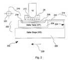
- the lithography machine 200includes a optical assembly 16 and a stage assembly 202 that includes a wafer table 204 and a wafer stage 206 .
- the wafer table 204is configured to support a wafer 208 (or any other type of work piece) under the optical assembly 16 .
- An environmental system 26surrounding the optical assembly 16 , is used to supply and remove immersion fluid 212 from the gap between the wafer 208 and the last optical element of the optical assembly 16 .
- a work piece exchange system 216including a wafer loader 218 (i.e., a robot) and an alignment tool 220 (i.e., a microscope and CCD camera), is configured to remove the wafer 208 on the wafer table 204 and replace it with a second wafer. This is typically accomplished using the wafer loader 218 to lift and remove the wafer 208 from the wafer table 204 . Subsequently, the second wafer (not shown) is placed onto the wafer chuck 218 , aligned using the alignment tool 220 , and then positioned under the optical assembly 16 on the wafer table 204 .
- a wafer loader 218i.e., a robot
- an alignment tool 220i.e., a microscope and CCD camera
- the wafer stage 206includes an immersion fluid containment system 214 that is configured to maintain the immersion fluid 212 in the gap adjacent to the last optical element of the optical assembly 16 during wafer exchange.
- the immersion fluid containment system 214includes a pad 222 that is adjacent to the wafer table 204 .
- a support member 224provided between the pad 222 and the wafer stage 206 , is used to support the pad 222 .
- the wafer table 204has a flat upper surface that is coplanar with a surface of the wafer 208 .
- the pad 222also has a flat upper surface that is coplanar with the upper surface of the wafer table 204 and the wafer surface.
- the pad 222is arranged adjacent to the wafer table 204 with a very small gap (e.g., 0.1-1.0 mm) so that the immersion fluid 212 is movable between the wafer table 204 and the pad 222 without leaking.
- the wafer stage 206is moved in the direction of arrow 226 so that the pad 222 is positioned under the optical assembly 16 in place of the wafer table 204 , maintaining the fluid in the gap or maintaining the size of the fluid gap.
- the wafer stageis moved back to its original position so that the pad 222 is removed from the gap as the second wafer is positioned under the optical assembly 16 .
- the pad 222is disposed continuously adjacent to the wafer table 204 with no gap. Vertical position and/or tilt of the wafer table 204 can be adjusted so that the wafer table surface is coplanar with the pad surface, before the wafer table 204 is moved out from under the optical assembly 16 . Maintaining the gap between the pad 222 and the optical assembly 16 is not limited to just a wafer exchange operation.
- the pad 222can be large enough to maintain the immersion fluid 212 in the space between the pad 222 and the optical assembly 16 during an alignment operation or a measurement operation. In those operations, a part of the area occupied by the immersion fluid 212 may be on the upper surface of the wafer table 204 .
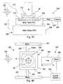
- the lithography machine 300includes an optical assembly 16 and a stage assembly 302 that includes a wafer table 304 and a wafer stage 306 .
- the wafer table 304is configured to support a wafer 308 (or any other type of work piece) under the optical assembly 16 .
- An environmental system 26surrounding the optical assembly 16 , is used to supply and remove immersion fluid 312 from the gap between the wafer 308 and the lower most optical element of the optical assembly 16 .
- a work piece exchange system 316including a wafer loader 318 and an alignment tool 320 , is configured to remove the wafer 308 on the wafer table 304 and replace it with a second wafer. This is accomplished using the wafer loader 318 to remove the wafer 308 from the wafer table. Subsequently, the second wafer (not shown) is placed onto the wafer chuck 318 , aligned using the alignment tool 320 , and then positioned under the optical assembly 16 . As best illustrated in FIG. 3B , a set of motors 322 are used to move the wafer assembly 302 including the wafer table 304 and wafer stage 306 in two degrees of freedom (X and Y) during operation. As noted above, the motors 322 can be any type of motors, such as linear motors, rotary motors, voice coil motors, etc.
- the immersion lithography machine 300also includes an immersion fluid containment system 324 that is configured to maintain the immersion fluid 312 in the space below the optical assembly 16 while the wafer table 304 is away from under the optical assembly.
- the immersion fluid containment system 324includes a pad 326 , a motor 328 , and a control system 330 .
- the pad 326can be positioned adjacent to the optical assembly 16 and the wafer table 304 .
- the wafer table 304has a flat upper surface that is coplanar with a surface of the wafer 308 .
- the pad 326has a flat upper surface that is coplanar with the upper surface of the wafer table 304 and the wafer surface.
- the pad 326is movable in the X and Y directions using the motor 328 , which is controlled by the control system 330 .
- the motor 328can be any type of motor as well as the motors 322 .
- the pad 326is positioned under the optical assembly 16 when the wafer table 304 (the wafer stage 306 ) is away from under the optical assembly 16 .
- the wafer table 304moves away from the optical assembly 16 .
- the control system 330directs the motor 328 to move pad 326 under the optical assembly 16 , replacing the wafer table 304 .
- the pad 326thus retains the immersion fluid 312 within the gap under the optical assembly 16 .
- the wafer table 304is repositioned under the optical assembly 16 .
- the control system 330directs the motor 328 to retract the pad 326 from the gap, preventing the escape of the immersion fluid 312 .
- the control system 330moves the wafer table 304 and the pad 326 with a small gap between the wafer table 304 and the pad 326 , while the immersion fluid 312 below the optical assembly 16 moves between the wafer table 304 and the pad 326 .
- the immersion fluid containment system 324thus maintains the immersion fluid 312 from the gap during wafer exchange.
- the wafer table 304(the wafer stage 306 ) and the pad 326 are movable separately. Therefore, the wafer table 304 is movable freely while the immersion fluid 312 is maintained in the space between the pad 326 and the optical assembly 16 .
- the control system 330may be a separate control system or it can be integrated into the control system used to control the motors 322 for positioning the wafer stage 306 and wafer table 304 . Vertical position and/or tilt of at least one of the wafer table 304 and the pad 326 may be adjusted so that the wafer table surface is coplanar with the pad surface, before the wafer table is moved out from under the optical assembly 16 .
- the operation, in which the wafer table 304 is away from the optical assembly 16is not necessarily limited to a wafer exchange operation.
- an alignment operation, a measurement operation or other operationmay be executed while maintaining the immersion fluid 312 in the space between the pad 326 and the optical assembly 16 .
- the lithography machine 400includes an optical assembly 16 and a stage assembly 402 that includes a wafer table 404 and a wafer stage 406 .
- the wafer table 404is configured to support a wafer 408 (or any other type of work piece) under the optical assembly 16 .
- An environmental system 26( 410 ), surrounding the optical assembly 16 , is used to supply and remove immersion fluid 412 from the gap between the wafer 408 and the lower most optical element of the optical assembly 16 .
- a work piece exchange system 416including a wafer loader 418 and an alignment tool 420 , is configured to remove the wafer 408 on the wafer table 404 and replace it with a second wafer. This is accomplished using the wafer loader 418 to remove the wafer 408 from the wafer table 404 . Subsequently, the second wafer (not shown) is placed onto the wafer chuck 418 , aligned using the alignment tool 420 , and then positioned under the optical assembly 16 as illustrated in the FIG. 4A .
- the immersion lithography machine 400also includes an immersion fluid containment system 424 that is configured to maintain the immersion fluid 412 in the space below the optical assembly 16 while the wafer table 404 is away from under the optical assembly 16 .
- the immersion fluid containment system 424includes a pad 426 , a first clamp 428 provided on the optical assembly 16 and a second clamp 430 provided on the wafer table 404 .
- the pad 426is held by the second clamp 430 in place on the wafer table 404 .
- the pad 426is detached from the wafer table 404 and held by the first clamp 428 to maintain the immersion fluid 412 between the optical assembly 16 and the pad 426 .
- the wafer table 404has a flat upper surface that is coplanar with a surface of the wafer 408 .
- the pad 426 held on the wafer table 404also has a flat upper surface that is coplanar with the upper surface of the wafer table 404 and the wafer surface. Therefore, the immersion pad 426 and wafer 408 can be moved under the optical assembly without the immersion fluid leaking.
- the clamps 428 and 430can be vacuum clamps, magnetic, electro-static, or mechanical.
- the pad 426is positioned on the wafer table 404 during exposure of the wafer 408 .
- the second clamp 430is used to hold the pad 426 in place on the table 404 during the wafer exposure.
- the wafer table 404is moved in the direction of arrow 432 so that the pad 426 is positioned under the optical assembly 16 in place of the wafer 408 .
- the second clamp 430 holding the pad 426 to the wafer table 404is released while first clamp 428 clamps the pad 426 to the optical assembly 16 .
- the immersion fluid 412is maintained under the optical assembly while the wafer 408 is exchanged.
- the wafer table 404is moved in the direction opposite arrow 432 so that the new wafer is positioned under the optical assembly. Prior to this motion, the first clamp 428 is released while the second clamp 430 again clamps the pad 426 to the wafer table 404 . In this embodiment, the wafer table 404 is freely movable while the pad 426 is clamped by the first clamp 428 .
- the operation, in which the pad 426 is clamped by the first clamp 428is not limited to only a wafer exchange operation.
- An alignment operation, a measurement operation, or any other operationcan be executed while the immersion fluid 412 is maintained in the space between the optical assembly 16 and the pad 426 clamped by the first clamp 428 .
- the clamp 428can be provided on the frame 12 or other support member, and the clamp 430 can be provided on the wafer stage 406 .
- the pad 426can be held on a movable member other than the stage assembly 402 .
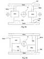
- FIGS. 5A and 5Bare top down views of two different twin stage immersion lithography systems according to other embodiments of the present invention.
- Motors 502are used to move or position the two stages WS 1 and WS 2 in the horizontal direction (in the drawings), whereas motors 504 are used to move or position the stages WS 1 and WS 2 in the vertical direction (in the drawings).
- the motors 502 and 504are used to alternatively position one stage under the optical assembly 16 while a wafer exchange and alignment is performed on the other stage. When the exposure of the wafer under the optical assembly 16 is complete, then the two stages are swapped and the above process is repeated.
- the various embodiments of the invention for maintaining immersion fluid in the gap under the optical assembly 16 as described and illustrated above with regard to FIGS. 2 through 4can be used with either twin stage arrangement. With regard the embodiment of FIG.
- each wafer stage SW 1 and SW 2 of either FIG. 5A or 5 Bcan be modified to include a pad 222 and a support member 224 .
- a single pad 326 , motor 328 , and control system 330could be used adjacent to the optical assembly 16 .
- the pad 326is movable separately from the stages SW 1 and SW 2 . During the time when stages SW 1 and SW 2 are to be swapped, the pad 326 is moved to under the optical assembly 16 to maintain the immersion fluid 312 below the optical assembly 16 .
- a detachable single padcan be used.
- the pad 426is used to maintain the immersion fluid in the gap as illustrated in FIG. 4B .
- the padis clamped onto the wafer table on the wafer stage that is being exposed. In this manner, only a single pad is needed for the two stages WS 1 and WS 2 .
- the second stagecan also be used as the pad.
- the immersion lithography system 600includes first stage 604 and second stage 606 .
- the two stagesare moved in the X and Y directions by motors 602 .
- the stages 604 and 606themselves are used to contain the immersion fluid in the gap.
- the first stage 604is positioned under the optical assembly 16 .
- the motors 602are used to position the second stage 606 with a second work piece adjacent to the first stage 604 . With the two stages positioned side-by-side, they substantially form a continuous surface.
- the motors 602are then used to move the two stages in unison so that the second stage 604 is position under the optical assembly 16 and the first stage is no longer under the optical assembly 16 .
- the immersion fluid in the gapis maintained by the second stage 606 , which forms the substantially continuous surface with the first stage.
- the second stage 606could also be a “pad” stage that contains a pad that is used to maintain the immersion liquid in the gap while a second work piece is being placed onto the first stage 604 .
- the motor arrangement shown in either FIG. 5A or 5 Bcould be used.
- FIGS. 6B-6Ea series of diagrams illustrating a work piece exchange according to one embodiment of the invention is illustrated.
- FIG. 6Bshows a wafer on stage 604 after exposure is completed.
- FIG. 6Cshows the second stage 606 in contact (or immediately adjacent) with the first stage 604 under the optical assembly 16 .
- FIG. 6Cshows a transfer taking place, i.e., the second stage 606 is positioned under the optical assembly 16 .
- the first stage 604is moved away from the optical assembly 16 .
- the two stages 604 and 606provide a continuous surface under the optical assembly 16 during a transfer, thus maintaining the immersion fluid in the gap.
- the second stage 606is a pad stage. This stage, however, could also be a work piece stage as noted above.
- the padcan be made of a number of different materials, such as ceramic, metal, plastic. These materials may also be coated with Teflon according to other embodiments.
- the size of the padalso should be sufficient to cover the area occupied by the immersion fluid.
- the surface of the last optical element of the optical assembly 16is constantly under immersion fluid environment, preventing the formation of a fluid mark (e.g. “a water mark”).
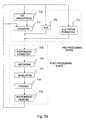
- step 701the work piece's function and performance characteristics are designed.
- step 702a mask (reticle) having a pattern is designed according to the previous designing step, and in a parallel step 703 a wafer is made from a silicon material.
- the mask pattern designed in step 702is exposed onto the wafer from step 703 in step 704 by a photolithography system described hereinabove in accordance with the invention.
- step 705the semiconductor work piece is assembled (including the dicing process, bonding process and packaging process); finally, the work piece is then inspected in step 706 .
- FIG. 7Billustrates a detailed flowchart example of the above-mentioned step 704 in the case of fabricating semiconductor work pieces.
- step 711oxidation step
- step 712CVD step
- step 713electrode formation step
- step 714ion implantation step
- steps 711 - 714form the preprocessing steps for wafers during wafer processing, and selection is made at each step according to processing requirements.
- step 715photoresist formation step
- step 716exposure step
- step 717developing step
- step 718etching step
- steps other than residual photoresistexposed material surface
- circuit patternsare formed by repetition of these preprocessing and post-processing steps.
Landscapes
- Physics & Mathematics (AREA)
- General Physics & Mathematics (AREA)
- Engineering & Computer Science (AREA)
- Condensed Matter Physics & Semiconductors (AREA)
- Manufacturing & Machinery (AREA)
- Computer Hardware Design (AREA)
- Microelectronics & Electronic Packaging (AREA)
- Power Engineering (AREA)
- Health & Medical Sciences (AREA)
- Optics & Photonics (AREA)
- Environmental & Geological Engineering (AREA)
- Epidemiology (AREA)
- Public Health (AREA)
- Toxicology (AREA)
- Exposure And Positioning Against Photoresist Photosensitive Materials (AREA)
- Exposure Of Semiconductors, Excluding Electron Or Ion Beam Exposure (AREA)
- Container, Conveyance, Adherence, Positioning, Of Wafer (AREA)
Abstract
Description
This is a Divisional of U.S. patent application Ser. No. 11/237,721 filed Sep. 29, 2005, which in turn is a Continuation of International Application No. PCT/IB2004/001259 filed Mar. 17, 2004, which claims the benefit of U.S. Provisional Application No. 60/462,499 filed on Apr. 11, 2003. The entire disclosures of the prior applications are incorporated herein by reference in their entireties.
Lithography systems are commonly used to transfer images from a reticle onto a semiconductor wafer during semiconductor processing. A typical lithography system includes an optical assembly, a reticle stage for holding a reticle defining a pattern, a wafer stage assembly that positions a semiconductor wafer, and a measurement system that precisely monitors the position of the reticle and the wafer. During operation, an image defined by the reticle is projected by the optical assembly onto the wafer. The projected image is typically the size of one or more die on the wafer. After an exposure, the wafer stage assembly moves the wafer and then another exposure takes place. This process is repeated until all the die on the wafer are exposed. The wafer is then removed and a new wafer is exchanged in its place.
Immersion lithography systems utilize a layer of immersion fluid that completely fills a gap between the optical assembly and the wafer during the exposure of the wafer. The optic properties of the immersion fluid, along with the optical assembly, allow the projection of smaller feature sizes than is currently possible using standard optical lithography. For example, immersion lithography is currently being considered for next generation semiconductor technologies including 65 nanometers, 45 nanometers, and beyond. Immersion lithography therefore represents a significant technological breakthrough that will likely enable the continued use of optical lithography for the foreseeable future.
After a wafer is exposed, it is removed and exchanged with a new wafer. As currently contemplated in immersion systems, the immersion fluid would be removed from the gap and then replenished after the wafer is exchanged. More specifically, when a wafer is to be exchanged, the fluid supply to the gap is turned off, the fluid is removed from the gap (i.e., by vacuum), the old wafer is removed, a new wafer is aligned and placed under the optical assembly, and then the gap is re-filled with fresh immersion fluid. Once all of the above steps are complete, exposure of the new wafer can begin.
Wafer exchange with immersion lithography as described above is problematic for a number of reasons. The repeated filling and draining of the gap may cause variations in the immersion fluid and may cause bubbles to form within the immersion fluid. Bubbles and the unsteady fluid may interfere with the projection of the image on the reticle onto the wafer, thereby reducing yields. The overall process also involves many steps and is time consuming, which reduces the overall throughput of the machine.
An apparatus and method for maintaining immersion fluid in the gap adjacent to the projection lens when the wafer stage moves away from the projection lens, for example during wafer exchange, is therefore needed.
An apparatus and method maintain immersion fluid in the gap adjacent to the projection lens in a lithography machine. The apparatus and method include an optical assembly that projects an image onto a work piece and a stage assembly including a work piece table that supports the work piece adjacent to the optical assembly. An environmental system is provided to supply and remove an immersion fluid from the gap. After exposure of the work piece is complete, an exchange system removes the work piece and replaces it with a second work piece. An immersion fluid containment system is provided to maintain the immersion fluid in the gap when the work piece table moves away from the projection lens. The gap therefore does not have to be refilled with immersion fluid when the first work piece is replaced with a second work piece.
The invention will be described in conjunction with the following drawings of exemplary embodiments in which like reference numerals designate like elements, and in which:
In one embodiment, thelithography machine 10 is used to transfer a pattern (not shown) of an integrated circuit from areticle 28 onto a semiconductor wafer30 (illustrated in phantom). Thelithography machine 10 mounts to amounting base 32, e.g., the ground, a base, or floor or some other supporting structure.
In various embodiments of the invention, thelithography machine 10 can be used as a scanning type photolithography system that exposes the pattern from thereticle 28 onto thewafer 30 with thereticle 28 and thewafer 30 moving synchronously. In a scanning type lithographic machine, thereticle 28 is moved perpendicularly to an optical axis of theoptical assembly 16 by thereticle stage assembly 18, and thewafer 30 is moved perpendicularly to the optical axis of theoptical assembly 16 by thewafer stage assembly 20. Scanning of thereticle 28 and thewafer 30 occurs while thereticle 28 and thewafer 30 are moving synchronously.
Alternatively, thelithography machine 10 can be a step-and-repeat type photolithography system that exposes thereticle 28 while thereticle 28 and thewafer 30 are stationary. In the step and repeat process, thewafer 30 is in a constant position relative to thereticle 28 and theoptical assembly 16 during the exposure of an individual field. Subsequently, between consecutive exposure steps, thewafer 30 is consecutively moved with thewafer stage assembly 20 perpendicularly to the optical axis of theoptical assembly 16 so that the next field of thewafer 30 is brought into position relative to theoptical assembly 16 and thereticle 28 for exposure. Following this process, the images on thereticle 28 are sequentially exposed onto the fields of thewafer 30, and then the next field of thewafer 30 is brought into position relative to theoptical assembly 16 and thereticle 28.
However, the use of thelithography machine 10 provided herein is not necessarily limited to a photolithography for semiconductor manufacturing. Thelithography machine 10, for example, can be used as an LCD photolithography system that exposes a liquid crystal display work piece pattern onto a rectangular glass plate or a photolithography system for manufacturing a thin film magnetic head. Accordingly, the term “work piece” is generically used herein to refer to any device that may be patterned using lithography, such as but not limited to wafers or LCD substrates.
Theapparatus frame 12 supports the components of thelithography machine 10. Theapparatus frame 12 illustrated inFIG. 1 supports thereticle stage assembly 18, thewafer stage assembly 20, theoptical assembly 16 and theillumination system 14 above the mountingbase 32.
Theillumination system 14 includes anillumination source 34 and an illuminationoptical assembly 36. Theillumination source 34 emits a beam (irradiation) of light energy. The illuminationoptical assembly 36 guides the beam of light energy from theillumination source 34 to theoptical assembly 16. The beam illuminates selectively different portions of thereticle 28 and exposes thewafer 30. InFIG. 1 , theillumination source 34 is illustrated as being supported above thereticle stage assembly 18. Typically, however, theillumination source 34 is secured to one of the sides of theapparatus frame 12 and the energy beam from theillumination source 34 is directed to above thereticle stage assembly 18 with the illuminationoptical assembly 36.
Theillumination source 34 can be a g-line source (436 nm), an i-line source (365 nm), a KrF excimer laser (248 nm), an ArF excimer laser (193 nm) or a F2laser (157 nm). Alternatively, theillumination source 34 can generate an x-ray.
Theoptical assembly 16 projects and/or focuses the light passing through thereticle 28 to thewafer 30. Depending upon the design of thelithography machine 10, theoptical assembly 16 can magnify or reduce the image illuminated on thereticle 28. Theoptical assembly 16 need not be limited to a reduction system. It could also be a 1× or greater magnification system.
Also, with an exposure work piece that employs vacuum ultra-violet radiation (VUV) ofwavelength 200 nm or lower, use of a catadioptric type optical system can be considered. Examples of a catadioptric type of optical system are disclosed in Japanese Laid-Open Patent Application Publication No. 8-171054 and its counterpart U.S. Pat. No. 5,668,672, as well as Japanese Laid-Open Patent Publication No. 10-20195 and its counterpart U.S. Pat. No. 5,835,275. In these cases, the reflecting optical system can be a catadioptric optical system incorporating a beam splitter and concave mirror. Japanese Laid-Open Patent Application Publication No. 8-334695 and its counterpart U.S. Pat. No. 5,689,377 as well as Japanese Laid-Open Patent Application Publication No. 10-3039 and its counterpart U.S. Pat. No. 873,605 (Application Date: Jun. 12, 1997) also use a reflecting-refracting type of optical system incorporating a concave mirror, etc., but without a beam splitter, and also can be employed with this invention. The disclosures of the above-mentioned U.S. patents and applications, as well as the Japanese Laid-Open patent application publications are incorporated herein by reference in their entireties.
Thereticle stage assembly 18 holds and positions thereticle 28 relative to theoptical assembly 16 and thewafer 30. In one embodiment, thereticle stage assembly 18 includes areticle stage 38 that retains thereticle 28 and a reticlestage mover assembly 40 that moves and positions thereticle stage 38 andreticle 28.
Eachstage mover assembly respective stage stage mover assembly respective stage stage mover assembly 40 and the work piecestage mover assembly 44 can each include one or more movers, such as rotary motors, voice coil motors, linear motors utilizing a Lorentz force to generate drive force, electromagnetic movers, planar motors, or some other force movers.
In photolithography systems, when linear motors (see U.S. Pat. Nos. 5,623,853 or 5,528,118 which are incorporated by reference herein in their entireties) are used in the wafer stage assembly or the reticle stage assembly, the linear motors can be either an air levitation type employing air bearings or a magnetic levitation type using Lorentz force or reactance force. Additionally, the stage could move along a guide, or it could be a guideless type stage that uses no guide.
Alternatively, one of the stages could be driven by a planar motor, which drives the stage by an electromagnetic force generated by a magnet unit having two-dimensionally arranged magnets and an armature coil unit having two-dimensionally arranged coils in facing positions. With this type of driving system, either the magnet unit or the armature coil unit is connected to the stage base and the other unit is mounted on the moving plane side of the stage.
Movement of the stages as described above generates reaction forces that can affect performance of the photolithography system. Reaction forces generated by the wafer (substrate) stage motion can be mechanically transferred to the floor (ground) by use of a frame member as described in U.S. Pat. No. 5,528,100 and Japanese Laid-Open Patent Application Publication No. 8-136475. Additionally, reaction forces generated by the reticle (mask) stage motion can be mechanically transferred to the floor (ground) by use of a frame member as described in U.S. Pat. No. 5,874,820 and Japanese Laid-Open Patent Application Publication No. 8-330224. The disclosures of U.S. Pat. Nos. 5,528,100 and 5,874,820 and Japanese Paid-Open Patent Application Publication Nos. 8-136475 and 8-330224 are incorporated herein by reference in their entireties.
Themeasurement system 22 monitors movement of thereticle 28 and thewafer 30 relative to theoptical assembly 16 or some other reference. With this information, thecontrol system 24 can control thereticle stage assembly 18 to precisely position thereticle 28 and the workpiece stage assembly 20 to precisely position thewafer 30. The design of themeasurement system 22 can vary. For example, themeasurement system 22 can utilize multiple laser interferometers, encoders, mirrors, and/or other measuring devices.
Thecontrol system 24 receives information from themeasurement system 22 and controls thestage assemblies reticle 28 and thewafer 30. Additionally, thecontrol system 24 can control the operation of the components of theenvironmental system 26. Thecontrol system 24 can include one or more processors and circuits.
Theenvironmental system 26 controls the environment in a gap (not shown) between theoptical assembly 16 and thewafer 30. The gap includes an imaging field. The imaging field includes the area adjacent to the region of thewafer 30 that is being exposed and the area in which the beam of light energy travels between theoptical assembly 16 and thewafer 30. With this design, theenvironmental system 26 can control the environment in the imaging field. The desired environment created and/or controlled in the gap by theenvironmental system 26 can vary accordingly to thewafer 30 and the design of the rest of the components of thelithography machine 10, including theillumination system 14. For example, the desired controlled environment can be a fluid such as water. Alternatively, the desired controlled environment can be another type of fluid such as a gas. In various embodiments, the gap may range from 0.1 mm to 10 mm in height between top surface of thewafer 30 and the last optical element of theoptical assembly 16.
In one embodiment, theenvironmental system 26 fills the imaging field and the rest of the gap with an immersion fluid. The design of theenvironmental system 26 and the components of theenvironmental system 26 can be varied. In different embodiments, theenvironmental system 26 delivers and/or injects immersion fluid into the gap using spray nozzles, electro-kinetic sponges, porous materials, etc. and removes the fluid from the gap using vacuum pumps, sponges, and the like. The design of theenvironmental system 26 can vary. For example, it can inject the immersion fluid at one or more locations at or near the gap. Further, the immersion fluid system can assist in removing and/or scavenging the immersion fluid at one or more locations at or near thework piece 30, the gap and/or the edge of theoptical assembly 16. For additional details on various environmental systems, see U.S. provisional patent applications 60/462,142 entitled “Immersion Lithography Fluid Control System” filed on Apr. 9, 2003, 60/462,112 entitled “Vacuum Ring System and Wick Ring System for Immersion Lithography” filed on Apr. 10, 2003, 60/500,312 entitled “Noiseless Fluid Recovery With Porous Material” filed on Sep. 3, 2003, and 60/541,329 entitled “Nozzle Design for Immersion Lithography” filed on Feb. 2, 2004, all incorporated by reference herein in their entireties.
Referring toFIG. 2 , a cross section of a lithography machine illustrating one embodiment of the invention is shown. Thelithography machine 200 includes aoptical assembly 16 and astage assembly 202 that includes a wafer table204 and awafer stage 206. The wafer table204 is configured to support a wafer208 (or any other type of work piece) under theoptical assembly 16. Anenvironmental system 26, surrounding theoptical assembly 16, is used to supply and removeimmersion fluid 212 from the gap between thewafer 208 and the last optical element of theoptical assembly 16. A workpiece exchange system 216, including a wafer loader218 (i.e., a robot) and an alignment tool220 (i.e., a microscope and CCD camera), is configured to remove thewafer 208 on the wafer table204 and replace it with a second wafer. This is typically accomplished using thewafer loader 218 to lift and remove thewafer 208 from the wafer table204. Subsequently, the second wafer (not shown) is placed onto thewafer chuck 218, aligned using thealignment tool 220, and then positioned under theoptical assembly 16 on the wafer table204.
With this embodiment, thewafer stage 206 includes an immersionfluid containment system 214 that is configured to maintain theimmersion fluid 212 in the gap adjacent to the last optical element of theoptical assembly 16 during wafer exchange. The immersionfluid containment system 214 includes apad 222 that is adjacent to the wafer table204. Asupport member 224, provided between thepad 222 and thewafer stage 206, is used to support thepad 222. The wafer table204 has a flat upper surface that is coplanar with a surface of thewafer 208. Thepad 222 also has a flat upper surface that is coplanar with the upper surface of the wafer table204 and the wafer surface. Thepad 222 is arranged adjacent to the wafer table204 with a very small gap (e.g., 0.1-1.0 mm) so that theimmersion fluid 212 is movable between the wafer table204 and thepad 222 without leaking. During a wafer exchange, thewafer stage 206 is moved in the direction ofarrow 226 so that thepad 222 is positioned under theoptical assembly 16 in place of the wafer table204, maintaining the fluid in the gap or maintaining the size of the fluid gap. After the new wafer has been aligned, the wafer stage is moved back to its original position so that thepad 222 is removed from the gap as the second wafer is positioned under theoptical assembly 16. In various embodiments, thepad 222 is disposed continuously adjacent to the wafer table204 with no gap. Vertical position and/or tilt of the wafer table204 can be adjusted so that the wafer table surface is coplanar with the pad surface, before the wafer table204 is moved out from under theoptical assembly 16. Maintaining the gap between thepad 222 and theoptical assembly 16 is not limited to just a wafer exchange operation. Thepad 222 can be large enough to maintain theimmersion fluid 212 in the space between thepad 222 and theoptical assembly 16 during an alignment operation or a measurement operation. In those operations, a part of the area occupied by theimmersion fluid 212 may be on the upper surface of the wafer table204.
Referring toFIGS. 3A and 3B , a cross section and a top down view of another immersion lithography machine according to another embodiment of the present invention are shown. Thelithography machine 300 includes anoptical assembly 16 and astage assembly 302 that includes a wafer table304 and awafer stage 306. The wafer table304 is configured to support a wafer308 (or any other type of work piece) under theoptical assembly 16. Anenvironmental system 26, surrounding theoptical assembly 16, is used to supply and removeimmersion fluid 312 from the gap between thewafer 308 and the lower most optical element of theoptical assembly 16. A workpiece exchange system 316, including awafer loader 318 and analignment tool 320, is configured to remove thewafer 308 on the wafer table304 and replace it with a second wafer. This is accomplished using thewafer loader 318 to remove thewafer 308 from the wafer table. Subsequently, the second wafer (not shown) is placed onto thewafer chuck 318, aligned using thealignment tool 320, and then positioned under theoptical assembly 16. As best illustrated inFIG. 3B , a set ofmotors 322 are used to move thewafer assembly 302 including the wafer table304 andwafer stage 306 in two degrees of freedom (X and Y) during operation. As noted above, themotors 322 can be any type of motors, such as linear motors, rotary motors, voice coil motors, etc.
Theimmersion lithography machine 300 also includes an immersionfluid containment system 324 that is configured to maintain theimmersion fluid 312 in the space below theoptical assembly 16 while the wafer table304 is away from under the optical assembly. The immersionfluid containment system 324 includes apad 326, amotor 328, and acontrol system 330. Thepad 326 can be positioned adjacent to theoptical assembly 16 and the wafer table304. The wafer table304 has a flat upper surface that is coplanar with a surface of thewafer 308. Thepad 326 has a flat upper surface that is coplanar with the upper surface of the wafer table304 and the wafer surface. Thepad 326 is movable in the X and Y directions using themotor 328, which is controlled by thecontrol system 330. Themotor 328 can be any type of motor as well as themotors 322. Thepad 326 is positioned under theoptical assembly 16 when the wafer table304 (the wafer stage306) is away from under theoptical assembly 16. During a wafer exchange, the wafer table304 moves away from theoptical assembly 16. Simultaneously, thecontrol system 330 directs themotor 328 to movepad 326 under theoptical assembly 16, replacing the wafer table304. Thepad 326 thus retains theimmersion fluid 312 within the gap under theoptical assembly 16. After the new wafer has been aligned using thealignment tool 320, the wafer table304 is repositioned under theoptical assembly 16. At the same time, thecontrol system 330 directs themotor 328 to retract thepad 326 from the gap, preventing the escape of theimmersion fluid 312. In the wafer exchange operation, thecontrol system 330 moves the wafer table304 and thepad 326 with a small gap between the wafer table304 and thepad 326, while theimmersion fluid 312 below theoptical assembly 16 moves between the wafer table304 and thepad 326. The immersionfluid containment system 324 thus maintains theimmersion fluid 312 from the gap during wafer exchange. In this embodiment, the wafer table304 (the wafer stage306) and thepad 326 are movable separately. Therefore, the wafer table304 is movable freely while theimmersion fluid 312 is maintained in the space between thepad 326 and theoptical assembly 16. In various embodiments of the invention, thecontrol system 330 may be a separate control system or it can be integrated into the control system used to control themotors 322 for positioning thewafer stage 306 and wafer table304. Vertical position and/or tilt of at least one of the wafer table304 and thepad 326 may be adjusted so that the wafer table surface is coplanar with the pad surface, before the wafer table is moved out from under theoptical assembly 16. The operation, in which the wafer table304 is away from theoptical assembly 16, is not necessarily limited to a wafer exchange operation. For example, an alignment operation, a measurement operation or other operation may be executed while maintaining theimmersion fluid 312 in the space between thepad 326 and theoptical assembly 16.
Referring toFIGS. 4A and 4B , two cross sections of an immersion lithography machine are shown. Thelithography machine 400 includes anoptical assembly 16 and astage assembly 402 that includes a wafer table404 and awafer stage 406. The wafer table404 is configured to support a wafer408 (or any other type of work piece) under theoptical assembly 16. An environmental system26 (410), surrounding theoptical assembly 16, is used to supply and removeimmersion fluid 412 from the gap between thewafer 408 and the lower most optical element of theoptical assembly 16. A workpiece exchange system 416, including awafer loader 418 and analignment tool 420, is configured to remove thewafer 408 on the wafer table404 and replace it with a second wafer. This is accomplished using thewafer loader 418 to remove thewafer 408 from the wafer table404. Subsequently, the second wafer (not shown) is placed onto thewafer chuck 418, aligned using thealignment tool 420, and then positioned under theoptical assembly 16 as illustrated in theFIG. 4A .
Theimmersion lithography machine 400 also includes an immersionfluid containment system 424 that is configured to maintain theimmersion fluid 412 in the space below theoptical assembly 16 while the wafer table404 is away from under theoptical assembly 16. The immersionfluid containment system 424 includes apad 426, afirst clamp 428 provided on theoptical assembly 16 and asecond clamp 430 provided on the wafer table404. When theimmersion fluid 412 is between theoptical assembly 16 and the wafer table404 (or the wafer408), thepad 426 is held by thesecond clamp 430 in place on the wafer table404. When the wafer table404 is away from theoptical assembly 16, for example during a wafer exchange operation, thepad 426 is detached from the wafer table404 and held by thefirst clamp 428 to maintain theimmersion fluid 412 between theoptical assembly 16 and thepad 426. The wafer table404 has a flat upper surface that is coplanar with a surface of thewafer 408. Thepad 426 held on the wafer table404 also has a flat upper surface that is coplanar with the upper surface of the wafer table404 and the wafer surface. Therefore, theimmersion pad 426 andwafer 408 can be moved under the optical assembly without the immersion fluid leaking. In various embodiments, theclamps
As best illustrated inFIG. 4A , thepad 426 is positioned on the wafer table404 during exposure of thewafer 408. Thesecond clamp 430 is used to hold thepad 426 in place on the table404 during the wafer exposure. During a wafer exchange as illustrated inFIG. 4B , the wafer table404 is moved in the direction ofarrow 432 so that thepad 426 is positioned under theoptical assembly 16 in place of thewafer 408. When this occurs, thesecond clamp 430 holding thepad 426 to the wafer table404 is released whilefirst clamp 428 clamps thepad 426 to theoptical assembly 16. As a result, theimmersion fluid 412 is maintained under the optical assembly while thewafer 408 is exchanged. After the new wafer has been aligned, the wafer table404 is moved in the direction oppositearrow 432 so that the new wafer is positioned under the optical assembly. Prior to this motion, thefirst clamp 428 is released while thesecond clamp 430 again clamps thepad 426 to the wafer table404. In this embodiment, the wafer table404 is freely movable while thepad 426 is clamped by thefirst clamp 428.
In various embodiments, the operation, in which thepad 426 is clamped by thefirst clamp 428, is not limited to only a wafer exchange operation. An alignment operation, a measurement operation, or any other operation can be executed while theimmersion fluid 412 is maintained in the space between theoptical assembly 16 and thepad 426 clamped by thefirst clamp 428. Also, theclamp 428 can be provided on theframe 12 or other support member, and theclamp 430 can be provided on thewafer stage 406. Thepad 426 can be held on a movable member other than thestage assembly 402.
Referring toFIG. 6A , a top down view of a twin stage lithography machine illustrating one embodiment of practicing the invention is shown. In this embodiment, theimmersion lithography system 600 includesfirst stage 604 andsecond stage 606. The two stages are moved in the X and Y directions bymotors 602. In this embodiment, thestages first stage 604 is positioned under theoptical assembly 16. When it is time for the work piece to be exchanged, themotors 602 are used to position thesecond stage 606 with a second work piece adjacent to thefirst stage 604. With the two stages positioned side-by-side, they substantially form a continuous surface. Themotors 602 are then used to move the two stages in unison so that thesecond stage 604 is position under theoptical assembly 16 and the first stage is no longer under theoptical assembly 16. Thus when the first work piece is moved away from theoptical assembly 16, the immersion fluid in the gap is maintained by thesecond stage 606, which forms the substantially continuous surface with the first stage. In various alternative embodiments, thesecond stage 606 could also be a “pad” stage that contains a pad that is used to maintain the immersion liquid in the gap while a second work piece is being placed onto thefirst stage 604. Similarly, the motor arrangement shown in eitherFIG. 5A or5B could be used.
Referring toFIGS. 6B-6E , a series of diagrams illustrating a work piece exchange according to one embodiment of the invention is illustrated.FIG. 6B shows a wafer onstage 604 after exposure is completed.FIG. 6C shows thesecond stage 606 in contact (or immediately adjacent) with thefirst stage 604 under theoptical assembly 16.FIG. 6C shows a transfer taking place, i.e., thesecond stage 606 is positioned under theoptical assembly 16. Finally, inFIG. 6E , thefirst stage 604 is moved away from theoptical assembly 16. As best illustrated inFIGS. 6C and 6D , the twostages optical assembly 16 during a transfer, thus maintaining the immersion fluid in the gap. In the embodiment shown, thesecond stage 606 is a pad stage. This stage, however, could also be a work piece stage as noted above.
In the various embodiments described above, the pad can be made of a number of different materials, such as ceramic, metal, plastic. These materials may also be coated with Teflon according to other embodiments. The size of the pad also should be sufficient to cover the area occupied by the immersion fluid. In the various embodiments described above, the surface of the last optical element of theoptical assembly 16 is constantly under immersion fluid environment, preventing the formation of a fluid mark (e.g. “a water mark”).
Semiconductor wafers can be fabricated using the above described systems, by the process shown generally inFIG. 7A . Instep 701 the work piece's function and performance characteristics are designed. Next, instep 702, a mask (reticle) having a pattern is designed according to the previous designing step, and in a parallel step703 a wafer is made from a silicon material. The mask pattern designed instep 702 is exposed onto the wafer fromstep 703 instep 704 by a photolithography system described hereinabove in accordance with the invention. Instep 705 the semiconductor work piece is assembled (including the dicing process, bonding process and packaging process); finally, the work piece is then inspected instep 706.
At each stage of wafer processing, when the above-mentioned preprocessing steps have been completed, the following post-processing steps are implemented. During post-processing, first, in step715 (photoresist formation step), photoresist is applied to a wafer. Next, in step716 (exposure step), the above-mentioned exposure work piece is used to transfer the circuit pattern of a mask (reticle) to a wafer. Then in step717 (developing step), the exposed wafer is developed, and in step718 (etching step), parts other than residual photoresist (exposed material surface) are removed by etching. In step719 (photoresist removal step), unnecessary photoresist remaining after etching is removed.
Multiple circuit patterns are formed by repetition of these preprocessing and post-processing steps.
While the particular lithography machines as shown and disclosed herein are fully capable of obtaining the objects and providing the advantages herein before stated, it is to be understood that they are merely illustrative embodiments of the invention, and that the invention is not limited to these embodiments.
Claims (18)
1. A lithographic projection apparatus comprising:
a substrate table on which a substrate is held;
a projection system that projects a patterned beam onto a target portion of the substrate held by the substrate table, an immersion liquid, through which the beam is to be projected, being in a space between the projection system and the substrate; and
a flat pad that keeps the projection system in contact with the immersion liquid when the substrate, at least while held on the substrate table, comes out of contact with the immersion liquid, the flat pad being separate from the substrate table.
2. An apparatus according toclaim 1 , wherein the flat pad is positionable opposite the projection system such that the immersion liquid can be confined between the projection system and the flat pad.
3. An apparatus according toclaim 2 , further comprising an attachment device that releasably attaches the flat pad over a final optical element of the projection system.
4. An apparatus according toclaim 3 , wherein the attachment device comprises a vacuum outlet that attracts the flat pad toward the projection system.
5. An apparatus according toclaim 2 , wherein the substrate table comprises a holding device that releasably holds the flat pad to the substrate table.
6. An apparatus according toclaim 2 , wherein, in a stowed position, the flat pad has a primary surface substantially co-planar with a surface of the substrate facing the projection system.
7. An apparatus according toclaim 2 , wherein the lithographic apparatus comprises a controller that moves the substrate table relative to the projection system so that the flat pad confines the immersion liquid between the flat pad and the projection system.
8. An apparatus according toclaim 1 , wherein the flat pad has a primary surface substantially co-planar with a surface of the substrate facing the projection system and is closely adjacent to an edge of the substrate.
9. An apparatus according toclaim 1 , further comprising a structure extending along at least a part of a boundary of the space between the projection system and the substrate table and wherein the flat pad, when keeping the projection system in contact with the immersion liquid, is positioned to cover the structure.
10. An apparatus according toclaim 1 , wherein the flat pad keeps the projection system in contact with the immersion liquid when the substrate is moved away from under the projection system.
11. A device manufacturing method comprising:
providing an immersion liquid to a space between a projection system and a substrate;
projecting a patterned beam of radiation, through the immersion liquid, onto a target portion of the substrate using the projection system; and
maintaining the projection system in contact with the immersion liquid when the substrate, at least while on a substrate table, comes out of contact with the immersion liquid by placing a flat pad, which is separate from the substrate table, adjacent to the projection system in place of the substrate.
12. A method according toclaim 11 , wherein maintaining the projection system in contact with liquid comprises positioning the flat pad on a side opposite the projection system such that liquid is confined between the projection system and the flat pad.
13. A method according toclaim 12 , further comprising releasably attaching the flat pad over a final optical element of the projection system.
14. A method according toclaim 13 , wherein releasably attaching comprises attaching the flat pad using vacuum.
15. A method according toclaim 12 , wherein the flat pad, when keeping the projection system in contact with the immersion liquid, is positioned to cover a structure that extends along at least a part of a boundary of the space between the projection system and the substrate table.
16. A method according toclaim 12 , comprising moving the substrate table relative to the projection system so that the flat pad confines the immersion liquid between the flat pad and the projection system.
17. A method according toclaim 11 , comprising providing the immersion liquid to a space between a final lens of the projection system and the substrate.
18. A method according toclaim 11 , wherein the maintaining comprises maintaining the projection system in contact with the immersion liquid after the substrate has been moved away from under the projection system.
Priority Applications (6)
| Application Number | Priority Date | Filing Date | Title |
|---|---|---|---|
| US11/822,804US8514367B2 (en) | 2003-04-11 | 2007-07-10 | Apparatus and method for maintaining immersion fluid in the gap under the projection lens during wafer exchange in an immersion lithography machine |
| US13/944,487US9329493B2 (en) | 2003-04-11 | 2013-07-17 | Apparatus and method for maintaining immersion fluid in the gap under the projection lens during wafer exchange in an immersion lithography machine |
| US13/945,201US8634057B2 (en) | 2003-04-11 | 2013-07-18 | Apparatus and method for maintaining immersion fluid in the gap under the projection lens during wafer exchange in an immersion lithography machine |
| US13/945,407US8610875B2 (en) | 2003-04-11 | 2013-07-18 | Apparatus and method for maintaining immersion fluid in the gap under the projection lens during wafer exchange in an immersion lithography machine |
| US13/946,317US8848166B2 (en) | 2003-04-11 | 2013-07-19 | Apparatus and method for maintaining immersion fluid in the gap under the projection lens during wafer exchange in an immersion lithography machine |
| US15/138,829US9500960B2 (en) | 2003-04-11 | 2016-04-26 | Apparatus and method for maintaining immersion fluid in the gap under the projection lens during wafer exchange in an immersion lithography machine |
Applications Claiming Priority (4)
| Application Number | Priority Date | Filing Date | Title |
|---|---|---|---|
| US46249903P | 2003-04-11 | 2003-04-11 | |
| PCT/IB2004/001259WO2004090577A2 (en) | 2003-04-11 | 2004-03-17 | Maintaining immersion fluid under a lithographic projection lens |
| US11/237,721US7372538B2 (en) | 2003-04-11 | 2005-09-29 | Apparatus and method for maintaining immerison fluid in the gap under the projection lens during wafer exchange in an immersion lithography machine |
| US11/822,804US8514367B2 (en) | 2003-04-11 | 2007-07-10 | Apparatus and method for maintaining immersion fluid in the gap under the projection lens during wafer exchange in an immersion lithography machine |
Related Parent Applications (1)
| Application Number | Title | Priority Date | Filing Date |
|---|---|---|---|
| US11/237,721DivisionUS7372538B2 (en) | 2003-04-11 | 2005-09-29 | Apparatus and method for maintaining immerison fluid in the gap under the projection lens during wafer exchange in an immersion lithography machine |
Related Child Applications (4)
| Application Number | Title | Priority Date | Filing Date |
|---|---|---|---|
| US13/944,487DivisionUS9329493B2 (en) | 2003-04-11 | 2013-07-17 | Apparatus and method for maintaining immersion fluid in the gap under the projection lens during wafer exchange in an immersion lithography machine |
| US13/945,201DivisionUS8634057B2 (en) | 2003-04-11 | 2013-07-18 | Apparatus and method for maintaining immersion fluid in the gap under the projection lens during wafer exchange in an immersion lithography machine |
| US13/945,407DivisionUS8610875B2 (en) | 2003-04-11 | 2013-07-18 | Apparatus and method for maintaining immersion fluid in the gap under the projection lens during wafer exchange in an immersion lithography machine |
| US13/946,317DivisionUS8848166B2 (en) | 2003-04-11 | 2013-07-19 | Apparatus and method for maintaining immersion fluid in the gap under the projection lens during wafer exchange in an immersion lithography machine |
Publications (2)
| Publication Number | Publication Date |
|---|---|
| US20070252965A1 US20070252965A1 (en) | 2007-11-01 |
| US8514367B2true US8514367B2 (en) | 2013-08-20 |
Family
ID=33159850
Family Applications (18)
| Application Number | Title | Priority Date | Filing Date |
|---|---|---|---|
| US11/237,721Expired - LifetimeUS7372538B2 (en) | 2003-04-11 | 2005-09-29 | Apparatus and method for maintaining immerison fluid in the gap under the projection lens during wafer exchange in an immersion lithography machine |
| US11/259,061Expired - LifetimeUS7327435B2 (en) | 2003-04-11 | 2005-10-27 | Apparatus and method for maintaining immersion fluid in the gap under the projection lens during wafer exchange in an immersion lithography machine |
| US11/785,539Expired - Fee RelatedUS9081298B2 (en) | 2003-04-11 | 2007-04-18 | Apparatus for maintaining immersion fluid in the gap under the projection lens during wafer exchange using a co-planar member in an immersion lithography machine |
| US11/798,262Expired - Fee RelatedUS7545479B2 (en) | 2003-04-11 | 2007-05-11 | Apparatus and method for maintaining immersion fluid in the gap under the projection lens during wafer exchange in an immersion lithography machine |
| US11/812,925Expired - Fee RelatedUS8848168B2 (en) | 2003-04-11 | 2007-06-22 | Apparatus and method for maintaining immersion fluid in the gap under the projection lens during wafer exchange in an immersion lithography machine |
| US11/822,804Expired - Fee RelatedUS8514367B2 (en) | 2003-04-11 | 2007-07-10 | Apparatus and method for maintaining immersion fluid in the gap under the projection lens during wafer exchange in an immersion lithography machine |
| US11/882,837Expired - Fee RelatedUS8269944B2 (en) | 2003-04-11 | 2007-08-06 | Apparatus and method for maintaining immersion fluid in the gap under the projection lens during wafer exchange in an immersion lithography machine |
| US11/984,980Expired - Fee RelatedUS8035795B2 (en) | 2003-04-11 | 2007-11-26 | Apparatus and method for maintaining immersion fluid in the gap under the protection lens during wafer exchange in an immersion lithography machine |
| US12/662,471Expired - Fee RelatedUS8351019B2 (en) | 2003-04-11 | 2010-04-19 | Apparatus and method for maintaining immersion fluid in the gap under the projection lens during wafer exchange in an immersion lithography machine |
| US12/923,822Expired - Fee RelatedUS8488100B2 (en) | 2003-04-11 | 2010-10-08 | Apparatus and method for maintaining immersion fluid in the gap under the projection lens during wafer exchange in an immersion lithography machine |
| US12/923,823Expired - Fee RelatedUS8879047B2 (en) | 2003-04-11 | 2010-10-08 | Apparatus and method for maintaining immersion fluid in the gap under the projection lens using a pad member or second stage during wafer exchange in an immersion lithography machine |
| US13/944,487Expired - LifetimeUS9329493B2 (en) | 2003-04-11 | 2013-07-17 | Apparatus and method for maintaining immersion fluid in the gap under the projection lens during wafer exchange in an immersion lithography machine |
| US13/945,201Expired - Fee RelatedUS8634057B2 (en) | 2003-04-11 | 2013-07-18 | Apparatus and method for maintaining immersion fluid in the gap under the projection lens during wafer exchange in an immersion lithography machine |
| US13/945,407Expired - Fee RelatedUS8610875B2 (en) | 2003-04-11 | 2013-07-18 | Apparatus and method for maintaining immersion fluid in the gap under the projection lens during wafer exchange in an immersion lithography machine |
| US13/946,317Expired - Fee RelatedUS8848166B2 (en) | 2003-04-11 | 2013-07-19 | Apparatus and method for maintaining immersion fluid in the gap under the projection lens during wafer exchange in an immersion lithography machine |
| US14/734,783Expired - Fee RelatedUS9946163B2 (en) | 2003-04-11 | 2015-06-09 | Apparatus and method for maintaining immersion fluid in the gap under the projection lens during wafer exchange in an immersion lithography machine |
| US15/138,829Expired - Fee RelatedUS9500960B2 (en) | 2003-04-11 | 2016-04-26 | Apparatus and method for maintaining immersion fluid in the gap under the projection lens during wafer exchange in an immersion lithography machine |
| US15/950,619AbandonedUS20180231898A1 (en) | 2003-04-11 | 2018-04-11 | Apparatus and method for maintaining immersion fluid in the gap under the projection lens during wafer exchange in an immersion lithography machine |
Family Applications Before (5)
| Application Number | Title | Priority Date | Filing Date |
|---|---|---|---|
| US11/237,721Expired - LifetimeUS7372538B2 (en) | 2003-04-11 | 2005-09-29 | Apparatus and method for maintaining immerison fluid in the gap under the projection lens during wafer exchange in an immersion lithography machine |
| US11/259,061Expired - LifetimeUS7327435B2 (en) | 2003-04-11 | 2005-10-27 | Apparatus and method for maintaining immersion fluid in the gap under the projection lens during wafer exchange in an immersion lithography machine |
| US11/785,539Expired - Fee RelatedUS9081298B2 (en) | 2003-04-11 | 2007-04-18 | Apparatus for maintaining immersion fluid in the gap under the projection lens during wafer exchange using a co-planar member in an immersion lithography machine |
| US11/798,262Expired - Fee RelatedUS7545479B2 (en) | 2003-04-11 | 2007-05-11 | Apparatus and method for maintaining immersion fluid in the gap under the projection lens during wafer exchange in an immersion lithography machine |
| US11/812,925Expired - Fee RelatedUS8848168B2 (en) | 2003-04-11 | 2007-06-22 | Apparatus and method for maintaining immersion fluid in the gap under the projection lens during wafer exchange in an immersion lithography machine |
Family Applications After (12)
| Application Number | Title | Priority Date | Filing Date |
|---|---|---|---|
| US11/882,837Expired - Fee RelatedUS8269944B2 (en) | 2003-04-11 | 2007-08-06 | Apparatus and method for maintaining immersion fluid in the gap under the projection lens during wafer exchange in an immersion lithography machine |
| US11/984,980Expired - Fee RelatedUS8035795B2 (en) | 2003-04-11 | 2007-11-26 | Apparatus and method for maintaining immersion fluid in the gap under the protection lens during wafer exchange in an immersion lithography machine |
| US12/662,471Expired - Fee RelatedUS8351019B2 (en) | 2003-04-11 | 2010-04-19 | Apparatus and method for maintaining immersion fluid in the gap under the projection lens during wafer exchange in an immersion lithography machine |
| US12/923,822Expired - Fee RelatedUS8488100B2 (en) | 2003-04-11 | 2010-10-08 | Apparatus and method for maintaining immersion fluid in the gap under the projection lens during wafer exchange in an immersion lithography machine |
| US12/923,823Expired - Fee RelatedUS8879047B2 (en) | 2003-04-11 | 2010-10-08 | Apparatus and method for maintaining immersion fluid in the gap under the projection lens using a pad member or second stage during wafer exchange in an immersion lithography machine |
| US13/944,487Expired - LifetimeUS9329493B2 (en) | 2003-04-11 | 2013-07-17 | Apparatus and method for maintaining immersion fluid in the gap under the projection lens during wafer exchange in an immersion lithography machine |
| US13/945,201Expired - Fee RelatedUS8634057B2 (en) | 2003-04-11 | 2013-07-18 | Apparatus and method for maintaining immersion fluid in the gap under the projection lens during wafer exchange in an immersion lithography machine |
| US13/945,407Expired - Fee RelatedUS8610875B2 (en) | 2003-04-11 | 2013-07-18 | Apparatus and method for maintaining immersion fluid in the gap under the projection lens during wafer exchange in an immersion lithography machine |
| US13/946,317Expired - Fee RelatedUS8848166B2 (en) | 2003-04-11 | 2013-07-19 | Apparatus and method for maintaining immersion fluid in the gap under the projection lens during wafer exchange in an immersion lithography machine |
| US14/734,783Expired - Fee RelatedUS9946163B2 (en) | 2003-04-11 | 2015-06-09 | Apparatus and method for maintaining immersion fluid in the gap under the projection lens during wafer exchange in an immersion lithography machine |
| US15/138,829Expired - Fee RelatedUS9500960B2 (en) | 2003-04-11 | 2016-04-26 | Apparatus and method for maintaining immersion fluid in the gap under the projection lens during wafer exchange in an immersion lithography machine |
| US15/950,619AbandonedUS20180231898A1 (en) | 2003-04-11 | 2018-04-11 | Apparatus and method for maintaining immersion fluid in the gap under the projection lens during wafer exchange in an immersion lithography machine |
Country Status (9)
| Country | Link |
|---|---|
| US (18) | US7372538B2 (en) |
| EP (8) | EP3141953A3 (en) |
| JP (12) | JP4315198B2 (en) |
| KR (15) | KR101225884B1 (en) |
| CN (3) | CN101980086B (en) |
| IL (5) | IL170735A (en) |
| SG (12) | SG139734A1 (en) |
| TW (16) | TWI545387B (en) |
| WO (1) | WO2004090577A2 (en) |
Cited By (1)
| Publication number | Priority date | Publication date | Assignee | Title |
|---|---|---|---|---|
| US10948830B1 (en) | 2019-12-23 | 2021-03-16 | Waymo Llc | Systems and methods for lithography |
Families Citing this family (221)
| Publication number | Priority date | Publication date | Assignee | Title |
|---|---|---|---|---|
| EP1420299B1 (en) | 2002-11-12 | 2011-01-05 | ASML Netherlands B.V. | Immersion lithographic apparatus and device manufacturing method |
| US10503084B2 (en) | 2002-11-12 | 2019-12-10 | Asml Netherlands B.V. | Lithographic apparatus and device manufacturing method |
| US7372541B2 (en) | 2002-11-12 | 2008-05-13 | Asml Netherlands B.V. | Lithographic apparatus and device manufacturing method |
| DE60335595D1 (en) | 2002-11-12 | 2011-02-17 | Asml Netherlands Bv | Immersion lithographic apparatus and method of making a device |
| CN100568101C (en) | 2002-11-12 | 2009-12-09 | Asml荷兰有限公司 | Photolithography apparatus and device manufacturing method |
| US7110081B2 (en) | 2002-11-12 | 2006-09-19 | Asml Netherlands B.V. | Lithographic apparatus and device manufacturing method |
| KR100585476B1 (en) | 2002-11-12 | 2006-06-07 | 에이에스엠엘 네델란즈 비.브이. | Lithographic Apparatus and Device Manufacturing Method |
| US9482966B2 (en) | 2002-11-12 | 2016-11-01 | Asml Netherlands B.V. | Lithographic apparatus and device manufacturing method |
| SG121822A1 (en)* | 2002-11-12 | 2006-05-26 | Asml Netherlands Bv | Lithographic apparatus and device manufacturing method |
| KR101101737B1 (en) | 2002-12-10 | 2012-01-05 | 가부시키가이샤 니콘 | Exposure apparatus, exposure method and method for manufacturing device |
| US7948604B2 (en) | 2002-12-10 | 2011-05-24 | Nikon Corporation | Exposure apparatus and method for producing device |
| EP1571694A4 (en) | 2002-12-10 | 2008-10-15 | Nikon Corp | Exposure apparatus and method for manufacturing device |
| US7242455B2 (en) | 2002-12-10 | 2007-07-10 | Nikon Corporation | Exposure apparatus and method for producing device |
| KR20120127755A (en) | 2002-12-10 | 2012-11-23 | 가부시키가이샤 니콘 | Exposure apparatus and method for manufacturing device |
| WO2004053955A1 (en) | 2002-12-10 | 2004-06-24 | Nikon Corporation | Exposure system and device producing method |
| JP4352874B2 (en) | 2002-12-10 | 2009-10-28 | 株式会社ニコン | Exposure apparatus and device manufacturing method |
| DE10261775A1 (en) | 2002-12-20 | 2004-07-01 | Carl Zeiss Smt Ag | Device for the optical measurement of an imaging system |
| EP2466623B1 (en) | 2003-02-26 | 2015-04-22 | Nikon Corporation | Exposure apparatus, exposure method, and method for producing device |
| KR20050110033A (en) | 2003-03-25 | 2005-11-22 | 가부시키가이샤 니콘 | Exposure system and device production method |
| EP1612850B1 (en) | 2003-04-07 | 2009-03-25 | Nikon Corporation | Exposure apparatus and method for manufacturing a device |
| WO2004093159A2 (en) | 2003-04-09 | 2004-10-28 | Nikon Corporation | Immersion lithography fluid control system |
| EP2950147B1 (en) | 2003-04-10 | 2017-04-26 | Nikon Corporation | Environmental system including vaccum scavenge for an immersion lithography apparatus |
| EP3062152B1 (en) | 2003-04-10 | 2017-12-20 | Nikon Corporation | Environmental system including vaccum scavenge for an immersion lithography apparatus |
| EP3352010A1 (en) | 2003-04-10 | 2018-07-25 | Nikon Corporation | Run-off path to collect liquid for an immersion lithography apparatus |
| KR101225884B1 (en)* | 2003-04-11 | 2013-01-28 | 가부시키가이샤 니콘 | Apparatus and method for maintaining immersion fluid in the gap under the projection lens during wafer exchange in an immersion lithography machine |
| CN101825847B (en) | 2003-04-11 | 2013-10-16 | 株式会社尼康 | Cleanup method for optics in immersion lithography |
| JP4582089B2 (en) | 2003-04-11 | 2010-11-17 | 株式会社ニコン | Liquid jet recovery system for immersion lithography |
| SG194246A1 (en) | 2003-04-17 | 2013-11-29 | Nikon Corp | Optical arrangement of autofocus elements for use with immersion lithography |
| TWI295414B (en) | 2003-05-13 | 2008-04-01 | Asml Netherlands Bv | Lithographic apparatus and device manufacturing method |
| KR20060009356A (en) | 2003-05-15 | 2006-01-31 | 가부시키가이샤 니콘 | Exposure apparatus and device manufacturing method |
| TW201806001A (en) | 2003-05-23 | 2018-02-16 | 尼康股份有限公司 | Exposure device and device manufacturing method |
| TWI421906B (en) | 2003-05-23 | 2014-01-01 | 尼康股份有限公司 | An exposure method, an exposure apparatus, and an element manufacturing method |
| KR101548832B1 (en) | 2003-05-28 | 2015-09-01 | 가부시키가이샤 니콘 | Exposure method, exposure device, and device manufacturing method |
| US7213963B2 (en) | 2003-06-09 | 2007-05-08 | Asml Netherlands B.V. | Lithographic apparatus and device manufacturing method |
| EP2261741A3 (en) | 2003-06-11 | 2011-05-25 | ASML Netherlands B.V. | Lithographic apparatus and device manufacturing method |
| US7317504B2 (en) | 2004-04-08 | 2008-01-08 | Asml Netherlands B.V. | Lithographic apparatus and device manufacturing method |
| KR101242815B1 (en) | 2003-06-13 | 2013-03-12 | 가부시키가이샤 니콘 | Exposure method, substrate stage, exposure apparatus and method for manufacturing device |
| US6867844B2 (en) | 2003-06-19 | 2005-03-15 | Asml Holding N.V. | Immersion photolithography system and method using microchannel nozzles |
| TW201721717A (en) | 2003-06-19 | 2017-06-16 | 尼康股份有限公司 | Exposure apparatus, exposure method, and device manufacturing method |
| JP3862678B2 (en) | 2003-06-27 | 2006-12-27 | キヤノン株式会社 | Exposure apparatus and device manufacturing method |
| US6809794B1 (en) | 2003-06-27 | 2004-10-26 | Asml Holding N.V. | Immersion photolithography system and method using inverted wafer-projection optics interface |
| EP1491956B1 (en) | 2003-06-27 | 2006-09-06 | ASML Netherlands B.V. | Lithographic apparatus and device manufacturing method |
| KR20060027832A (en) | 2003-07-01 | 2006-03-28 | 가부시키가이샤 니콘 | Method of Using Isotopically Specified Fluids as Optical Elements |
| EP3179309A1 (en) | 2003-07-08 | 2017-06-14 | Nikon Corporation | Wafer table for immersion lithography |
| EP1643543B1 (en) | 2003-07-09 | 2010-11-24 | Nikon Corporation | Exposure apparatus and method for manufacturing device |
| WO2005006415A1 (en) | 2003-07-09 | 2005-01-20 | Nikon Corporation | Exposure apparatus and method for manufacturing device |
| WO2005006418A1 (en) | 2003-07-09 | 2005-01-20 | Nikon Corporation | Exposure apparatus and method for manufacturing device |
| WO2005010960A1 (en) | 2003-07-25 | 2005-02-03 | Nikon Corporation | Inspection method and inspection device for projection optical system, and production method for projection optical system |
| EP1503244A1 (en) | 2003-07-28 | 2005-02-02 | ASML Netherlands B.V. | Lithographic projection apparatus and device manufacturing method |
| KR101641011B1 (en) | 2003-07-28 | 2016-07-19 | 가부시키가이샤 니콘 | Exposure apparatus, device producing method, and exposure apparatus controlling method |
| US7175968B2 (en) | 2003-07-28 | 2007-02-13 | Asml Netherlands B.V. | Lithographic apparatus, device manufacturing method and a substrate |
| US7326522B2 (en) | 2004-02-11 | 2008-02-05 | Asml Netherlands B.V. | Device manufacturing method and a substrate |
| US7779781B2 (en) | 2003-07-31 | 2010-08-24 | Asml Netherlands B.V. | Lithographic apparatus and device manufacturing method |
| TWI263859B (en) | 2003-08-29 | 2006-10-11 | Asml Netherlands Bv | Lithographic apparatus and device manufacturing method |
| KR101380989B1 (en) | 2003-08-29 | 2014-04-04 | 가부시키가이샤 니콘 | Exposure apparatus and device producing method |
| EP3223053A1 (en) | 2003-09-03 | 2017-09-27 | Nikon Corporation | Apparatus and method for providing fluid for immersion lithography |
| JP4444920B2 (en) | 2003-09-19 | 2010-03-31 | 株式会社ニコン | Exposure apparatus and device manufacturing method |
| EP2837969B1 (en) | 2003-09-29 | 2016-04-20 | Nikon Corporation | Exposure apparatus, exposure method, and method for producing device |
| JP2005136364A (en) | 2003-10-08 | 2005-05-26 | Zao Nikon Co Ltd | Substrate transport apparatus, exposure apparatus, and device manufacturing method |
| KR101203028B1 (en) | 2003-10-08 | 2012-11-21 | 가부시키가이샤 자오 니콘 | Substrate carrying apparatus, substrate carrying method, exposure apparatus, exposure method, and method for producing device |
| KR20060126949A (en) | 2003-10-08 | 2006-12-11 | 가부시키가이샤 니콘 | Substrate conveyance apparatus and substrate conveyance method, exposure apparatus, exposure method, and device manufacturing method |
| TWI553701B (en) | 2003-10-09 | 2016-10-11 | 尼康股份有限公司 | Exposure apparatus and exposure method, component manufacturing method |
| US7411653B2 (en) | 2003-10-28 | 2008-08-12 | Asml Netherlands B.V. | Lithographic apparatus |
| US7352433B2 (en) | 2003-10-28 | 2008-04-01 | Asml Netherlands B.V. | Lithographic apparatus and device manufacturing method |
| US7528929B2 (en) | 2003-11-14 | 2009-05-05 | Asml Netherlands B.V. | Lithographic apparatus and device manufacturing method |
| KR101394764B1 (en)* | 2003-12-03 | 2014-05-27 | 가부시키가이샤 니콘 | Exposure apparatus, exposure method, device producing method, and optical component |
| JP4720506B2 (en) | 2003-12-15 | 2011-07-13 | 株式会社ニコン | Stage apparatus, exposure apparatus, and exposure method |
| US7394521B2 (en) | 2003-12-23 | 2008-07-01 | Asml Netherlands B.V. | Lithographic apparatus and device manufacturing method |
| DE602005019689D1 (en) | 2004-01-20 | 2010-04-15 | Zeiss Carl Smt Ag | EXPOSURE DEVICE AND MEASURING DEVICE FOR A PROJECTION SECTOR |
| US7589822B2 (en) | 2004-02-02 | 2009-09-15 | Nikon Corporation | Stage drive method and stage unit, exposure apparatus, and device manufacturing method |
| WO2005076321A1 (en) | 2004-02-03 | 2005-08-18 | Nikon Corporation | Exposure apparatus and method of producing device |
| KR101851511B1 (en) | 2004-03-25 | 2018-04-23 | 가부시키가이샤 니콘 | Exposure apparatus and method for manufacturing device |
| US7034917B2 (en) | 2004-04-01 | 2006-04-25 | Asml Netherlands B.V. | Lithographic apparatus, device manufacturing method and device manufactured thereby |
| US7898642B2 (en) | 2004-04-14 | 2011-03-01 | Asml Netherlands B.V. | Lithographic apparatus and device manufacturing method |
| US7400460B2 (en)* | 2004-04-26 | 2008-07-15 | Carl Zeiss Smt Ag | Method for connection of an optical element to a mount structure |
| US8054448B2 (en) | 2004-05-04 | 2011-11-08 | Nikon Corporation | Apparatus and method for providing fluid for immersion lithography |
| US7616383B2 (en) | 2004-05-18 | 2009-11-10 | Asml Netherlands B.V. | Lithographic apparatus and device manufacturing method |
| CN100594430C (en) | 2004-06-04 | 2010-03-17 | 卡尔蔡司Smt股份公司 | System for measuring image quality of optical imaging system |
| EP3203498A1 (en) | 2004-06-09 | 2017-08-09 | Nikon Corporation | Exposure apparatus and device manufacturing method |
| KR101227290B1 (en) | 2004-06-09 | 2013-01-29 | 가부시키가이샤 니콘 | Substrate holding device, exposure apparatus having same, exposure method, method for producing device, and liquid repellent plate |
| US7463330B2 (en) | 2004-07-07 | 2008-12-09 | Asml Netherlands B.V. | Lithographic apparatus and device manufacturing method |
| JP4894515B2 (en) | 2004-07-12 | 2012-03-14 | 株式会社ニコン | Exposure apparatus, device manufacturing method, and liquid detection method |
| US8169591B2 (en)* | 2004-08-03 | 2012-05-01 | Nikon Corporation | Exposure apparatus, exposure method, and method for producing device |
| TW200615716A (en)* | 2004-08-05 | 2006-05-16 | Nikon Corp | Stage device and exposure device |
| KR20070048164A (en) | 2004-08-18 | 2007-05-08 | 가부시키가이샤 니콘 | Exposure apparatus and device manufacturing method |
| US7701550B2 (en) | 2004-08-19 | 2010-04-20 | Asml Netherlands B.V. | Lithographic apparatus and device manufacturing method |
| KR101364347B1 (en)* | 2004-10-15 | 2014-02-18 | 가부시키가이샤 니콘 | Exposure apparatus and device manufacturing method |
| US7119876B2 (en) | 2004-10-18 | 2006-10-10 | Asml Netherlands B.V. | Lithographic apparatus and device manufacturing method |
| CN101598903A (en)* | 2004-11-01 | 2009-12-09 | 株式会社尼康 | Exposure device and exposure method |
| JP4517354B2 (en)* | 2004-11-08 | 2010-08-04 | 株式会社ニコン | Exposure apparatus and device manufacturing method |
| US7583357B2 (en)* | 2004-11-12 | 2009-09-01 | Asml Netherlands B.V. | Lithographic apparatus and device manufacturing method |
| US7411657B2 (en) | 2004-11-17 | 2008-08-12 | Asml Netherlands B.V. | Lithographic apparatus and device manufacturing method |
| TWI588872B (en)* | 2004-11-18 | 2017-06-21 | 尼康股份有限公司 | Position measurement method, position control method, measurement method, loading method, exposure method and exposure apparatus, and device manufacturing method |
| JP4807629B2 (en)* | 2004-11-25 | 2011-11-02 | 株式会社ニコン | Exposure apparatus and device manufacturing method |
| US7446850B2 (en) | 2004-12-03 | 2008-11-04 | Asml Netherlands B.V. | Lithographic apparatus and device manufacturing method |
| JP4784513B2 (en) | 2004-12-06 | 2011-10-05 | 株式会社ニコン | Maintenance method, maintenance equipment, exposure apparatus, and device manufacturing method |
| US7196770B2 (en) | 2004-12-07 | 2007-03-27 | Asml Netherlands B.V. | Prewetting of substrate before immersion exposure |
| US7397533B2 (en) | 2004-12-07 | 2008-07-08 | Asml Netherlands B.V. | Lithographic apparatus and device manufacturing method |
| US7365827B2 (en) | 2004-12-08 | 2008-04-29 | Asml Netherlands B.V. | Lithographic apparatus and device manufacturing method |
| JP4752473B2 (en) | 2004-12-09 | 2011-08-17 | 株式会社ニコン | Exposure apparatus, exposure method, and device manufacturing method |
| US7352440B2 (en) | 2004-12-10 | 2008-04-01 | Asml Netherlands B.V. | Substrate placement in immersion lithography |
| US7403261B2 (en) | 2004-12-15 | 2008-07-22 | Asml Netherlands B.V. | Lithographic apparatus and device manufacturing method |
| US7528931B2 (en) | 2004-12-20 | 2009-05-05 | Asml Netherlands B.V. | Lithographic apparatus and device manufacturing method |
| US7880860B2 (en) | 2004-12-20 | 2011-02-01 | Asml Netherlands B.V. | Lithographic apparatus and device manufacturing method |
| US7405805B2 (en) | 2004-12-28 | 2008-07-29 | Asml Netherlands B.V. | Lithographic apparatus and device manufacturing method |
| US7491661B2 (en) | 2004-12-28 | 2009-02-17 | Asml Netherlands B.V. | Device manufacturing method, top coat material and substrate |
| US20060147821A1 (en) | 2004-12-30 | 2006-07-06 | Asml Netherlands B.V. | Lithographic apparatus and device manufacturing method |
| DE602006012746D1 (en) | 2005-01-14 | 2010-04-22 | Asml Netherlands Bv | Lithographic apparatus and manufacturing method |
| US8692973B2 (en) | 2005-01-31 | 2014-04-08 | Nikon Corporation | Exposure apparatus and method for producing device |
| KR101513840B1 (en) | 2005-01-31 | 2015-04-20 | 가부시키가이샤 니콘 | Exposure apparatus and method for manufacturing device |
| CN102360170B (en) | 2005-02-10 | 2014-03-12 | Asml荷兰有限公司 | Immersion liquid, exposure apparatus, and exposure process |
| US8018573B2 (en) | 2005-02-22 | 2011-09-13 | Asml Netherlands B.V. | Lithographic apparatus and device manufacturing method |
| US7224431B2 (en) | 2005-02-22 | 2007-05-29 | Asml Netherlands B.V. | Lithographic apparatus and device manufacturing method |
| US7378025B2 (en) | 2005-02-22 | 2008-05-27 | Asml Netherlands B.V. | Fluid filtration method, fluid filtered thereby, lithographic apparatus and device manufacturing method |
| US7428038B2 (en) | 2005-02-28 | 2008-09-23 | Asml Netherlands B.V. | Lithographic apparatus, device manufacturing method and apparatus for de-gassing a liquid |
| US7282701B2 (en) | 2005-02-28 | 2007-10-16 | Asml Netherlands B.V. | Sensor for use in a lithographic apparatus |
| US7324185B2 (en) | 2005-03-04 | 2008-01-29 | Asml Netherlands B.V. | Lithographic apparatus and device manufacturing method |
| US7684010B2 (en) | 2005-03-09 | 2010-03-23 | Asml Netherlands B.V. | Lithographic apparatus, device manufacturing method, seal structure, method of removing an object and a method of sealing |
| US7330238B2 (en) | 2005-03-28 | 2008-02-12 | Asml Netherlands, B.V. | Lithographic apparatus, immersion projection apparatus and device manufacturing method |
| JP4544303B2 (en)* | 2005-03-30 | 2010-09-15 | 株式会社ニコン | Exposure apparatus, exposure method, and device manufacturing method |
| US7411654B2 (en) | 2005-04-05 | 2008-08-12 | Asml Netherlands B.V. | Lithographic apparatus and device manufacturing method |
| US7291850B2 (en) | 2005-04-08 | 2007-11-06 | Asml Netherlands B.V. | Lithographic apparatus and device manufacturing method |
| USRE43576E1 (en) | 2005-04-08 | 2012-08-14 | Asml Netherlands B.V. | Dual stage lithographic apparatus and device manufacturing method |
| US20060232753A1 (en) | 2005-04-19 | 2006-10-19 | Asml Holding N.V. | Liquid immersion lithography system with tilted liquid flow |
| EP2527921A3 (en) | 2005-04-28 | 2017-10-18 | Nikon Corporation | Exposure method and exposure apparatus |
| US7317507B2 (en) | 2005-05-03 | 2008-01-08 | Asml Netherlands B.V. | Lithographic apparatus and device manufacturing method |
| US8248577B2 (en) | 2005-05-03 | 2012-08-21 | Asml Netherlands B.V. | Lithographic apparatus and device manufacturing method |
| US7433016B2 (en) | 2005-05-03 | 2008-10-07 | Asml Netherlands B.V. | Lithographic apparatus and device manufacturing method |
| US7751027B2 (en) | 2005-06-21 | 2010-07-06 | Asml Netherlands B.V. | Lithographic apparatus and device manufacturing method |
| US7652746B2 (en) | 2005-06-21 | 2010-01-26 | Asml Netherlands B.V. | Lithographic apparatus and device manufacturing method |
| US7468779B2 (en) | 2005-06-28 | 2008-12-23 | Asml Netherlands B.V. | Lithographic apparatus and device manufacturing method |
| US7834974B2 (en) | 2005-06-28 | 2010-11-16 | Asml Netherlands B.V. | Lithographic apparatus and device manufacturing method |
| US7474379B2 (en) | 2005-06-28 | 2009-01-06 | Asml Netherlands B.V. | Lithographic apparatus and device manufacturing method |
| US7583358B2 (en) | 2005-07-25 | 2009-09-01 | Micron Technology, Inc. | Systems and methods for retrieving residual liquid during immersion lens photolithography |
| EP1918983A4 (en) | 2005-08-05 | 2010-03-31 | Nikon Corp | Stage apparatus and exposure apparatus |
| US8054445B2 (en) | 2005-08-16 | 2011-11-08 | Asml Netherlands B.V. | Lithographic apparatus and device manufacturing method |
| WO2007029829A1 (en)* | 2005-09-09 | 2007-03-15 | Nikon Corporation | Exposure apparatus, exposure method, and device production method |
| US7417710B2 (en)* | 2005-09-26 | 2008-08-26 | Asml Netherlands B.V. | Lithographic apparatus and device manufacturing method |
| JP3997244B2 (en)* | 2005-10-04 | 2007-10-24 | キヤノン株式会社 | Exposure apparatus and device manufacturing method |
| JP4164508B2 (en)* | 2005-10-04 | 2008-10-15 | キヤノン株式会社 | Exposure apparatus and device manufacturing method |
| JP3997245B2 (en)* | 2005-10-04 | 2007-10-24 | キヤノン株式会社 | Exposure apparatus and device manufacturing method |
| US7411658B2 (en) | 2005-10-06 | 2008-08-12 | Asml Netherlands B.V. | Lithographic apparatus and device manufacturing method |
| JPWO2007055237A1 (en)* | 2005-11-09 | 2009-04-30 | 株式会社ニコン | Exposure apparatus, exposure method, and device manufacturing method |
| US7656501B2 (en) | 2005-11-16 | 2010-02-02 | Asml Netherlands B.V. | Lithographic apparatus |
| US7864292B2 (en) | 2005-11-16 | 2011-01-04 | Asml Netherlands B.V. | Lithographic apparatus and device manufacturing method |
| US7804577B2 (en) | 2005-11-16 | 2010-09-28 | Asml Netherlands B.V. | Lithographic apparatus |
| US7633073B2 (en) | 2005-11-23 | 2009-12-15 | Asml Netherlands B.V. | Lithographic apparatus and device manufacturing method |
| US7773195B2 (en) | 2005-11-29 | 2010-08-10 | Asml Holding N.V. | System and method to increase surface tension and contact angle in immersion lithography |
| US8125610B2 (en) | 2005-12-02 | 2012-02-28 | ASML Metherlands B.V. | Method for preventing or reducing contamination of an immersion type projection apparatus and an immersion type lithographic apparatus |
| US7420194B2 (en) | 2005-12-27 | 2008-09-02 | Asml Netherlands B.V. | Lithographic apparatus and substrate edge seal |
| US7839483B2 (en) | 2005-12-28 | 2010-11-23 | Asml Netherlands B.V. | Lithographic apparatus, device manufacturing method and a control system |
| US7649611B2 (en) | 2005-12-30 | 2010-01-19 | Asml Netherlands B.V. | Lithographic apparatus and device manufacturing method |
| US8472004B2 (en)* | 2006-01-18 | 2013-06-25 | Micron Technology, Inc. | Immersion photolithography scanner |
| EP3147710B1 (en)* | 2006-01-19 | 2019-04-10 | Nikon Corporation | Exposure apparatus, exposure method, and device manufacturing method |
| WO2007097380A1 (en)* | 2006-02-21 | 2007-08-30 | Nikon Corporation | Pattern forming apparatus, pattern forming method, mobile object driving system, mobile body driving method, exposure apparatus, exposure method and device manufacturing method |
| US8045134B2 (en) | 2006-03-13 | 2011-10-25 | Asml Netherlands B.V. | Lithographic apparatus, control system and device manufacturing method |
| US7760324B2 (en)* | 2006-03-20 | 2010-07-20 | Asml Netherlands B.V. | Lithographic apparatus and device manufacturing method |
| JP4889331B2 (en)* | 2006-03-22 | 2012-03-07 | 大日本スクリーン製造株式会社 | Substrate processing apparatus and substrate processing method |
| US8027019B2 (en) | 2006-03-28 | 2011-09-27 | Asml Netherlands B.V. | Lithographic apparatus and device manufacturing method |
| US7709813B2 (en) | 2006-04-03 | 2010-05-04 | Nikon Corporation | Incidence surfaces and optical windows that are solvophobic to immersion liquids |
| US9477158B2 (en) | 2006-04-14 | 2016-10-25 | Asml Netherlands B.V. | Lithographic apparatus and device manufacturing method |
| DE102006021797A1 (en) | 2006-05-09 | 2007-11-15 | Carl Zeiss Smt Ag | Optical imaging device with thermal damping |
| CN100456138C (en)* | 2006-06-13 | 2009-01-28 | 上海微电子装备有限公司 | Immersion liquid flow field maintenance system for immersion lithography machine |
| KR101698291B1 (en)* | 2006-08-31 | 2017-02-01 | 가부시키가이샤 니콘 | Mobile body drive method and mobile body drive system, pattern formation method and apparatus, exposure method and apparatus, and device manufacturing method |
| US7872730B2 (en)* | 2006-09-15 | 2011-01-18 | Nikon Corporation | Immersion exposure apparatus and immersion exposure method, and device manufacturing method |
| CN100468212C (en)* | 2006-09-22 | 2009-03-11 | 上海微电子装备有限公司 | Dual positioning exchange system |
| JP5120377B2 (en) | 2006-09-29 | 2013-01-16 | 株式会社ニコン | Exposure apparatus, exposure method, and device manufacturing method |
| US20080158531A1 (en) | 2006-11-15 | 2008-07-03 | Nikon Corporation | Exposure apparatus, exposure method, and method for producing device |
| US7973910B2 (en)* | 2006-11-17 | 2011-07-05 | Nikon Corporation | Stage apparatus and exposure apparatus |
| JP5089143B2 (en)* | 2006-11-20 | 2012-12-05 | キヤノン株式会社 | Immersion exposure equipment |
| US8045135B2 (en) | 2006-11-22 | 2011-10-25 | Asml Netherlands B.V. | Lithographic apparatus with a fluid combining unit and related device manufacturing method |
| US8634053B2 (en) | 2006-12-07 | 2014-01-21 | Asml Netherlands B.V. | Lithographic apparatus and device manufacturing method |
| US9632425B2 (en) | 2006-12-07 | 2017-04-25 | Asml Holding N.V. | Lithographic apparatus, a dryer and a method of removing liquid from a surface |
| US7728952B2 (en)* | 2007-01-25 | 2010-06-01 | Taiwan Semiconductor Manufacturing Company, Ltd. | Method and system for closing plate take-over in immersion lithography |
| US8237911B2 (en)* | 2007-03-15 | 2012-08-07 | Nikon Corporation | Apparatus and methods for keeping immersion fluid adjacent to an optical assembly during wafer exchange in an immersion lithography machine |
| US7841352B2 (en) | 2007-05-04 | 2010-11-30 | Asml Netherlands B.V. | Cleaning device, a lithographic apparatus and a lithographic apparatus cleaning method |
| US8947629B2 (en) | 2007-05-04 | 2015-02-03 | Asml Netherlands B.V. | Cleaning device, a lithographic apparatus and a lithographic apparatus cleaning method |
| JP2009033111A (en)* | 2007-05-28 | 2009-02-12 | Nikon Corp | Exposure apparatus, device manufacturing method, cleaning apparatus, cleaning method, and exposure method |
| US8279399B2 (en) | 2007-10-22 | 2012-10-02 | Nikon Corporation | Exposure apparatus, exposure method, and device manufacturing method |
| KR101470671B1 (en) | 2007-11-07 | 2014-12-08 | 가부시키가이샤 니콘 | Exposure apparatus, exposure method, and device manufacturing method |
| SG183058A1 (en)* | 2007-12-17 | 2012-08-30 | Nikon Corp | Exposure apparatus, exposure method and device manufacturing method |
| US8451425B2 (en) | 2007-12-28 | 2013-05-28 | Nikon Corporation | Exposure apparatus, exposure method, cleaning apparatus, and device manufacturing method |
| JP2009182110A (en)* | 2008-01-30 | 2009-08-13 | Nikon Corp | Exposure apparatus, exposure method, and device manufacturing method |
| US8610873B2 (en)* | 2008-03-17 | 2013-12-17 | Nikon Corporation | Immersion lithography apparatus and method having movable liquid diverter between immersion liquid confinement member and substrate |
| US20100039628A1 (en)* | 2008-03-19 | 2010-02-18 | Nikon Corporation | Cleaning tool, cleaning method, and device fabricating method |
| US8654306B2 (en)* | 2008-04-14 | 2014-02-18 | Nikon Corporation | Exposure apparatus, cleaning method, and device fabricating method |
| US9176393B2 (en) | 2008-05-28 | 2015-11-03 | Asml Netherlands B.V. | Lithographic apparatus and a method of operating the apparatus |
| US20100053588A1 (en)* | 2008-08-29 | 2010-03-04 | Nikon Corporation | Substrate Stage movement patterns for high throughput While Imaging a Reticle to a pair of Imaging Locations |
| US20100060106A1 (en)* | 2008-09-10 | 2010-03-11 | Hiwin Mikrosystem Corp. | Linear planar servomotor with spare-mover standby area |
| DE102009015717B4 (en)* | 2009-03-31 | 2012-12-13 | Globalfoundries Dresden Module One Limited Liability Company & Co. Kg | Method and system for detecting particle contamination in an immersion lithography apparatus |
| US8970820B2 (en) | 2009-05-20 | 2015-03-03 | Nikon Corporation | Object exchange method, exposure method, carrier system, exposure apparatus, and device manufacturing method |
| US8792084B2 (en) | 2009-05-20 | 2014-07-29 | Nikon Corporation | Exposure apparatus, exposure method, and device manufacturing method |
| US20100294742A1 (en)* | 2009-05-22 | 2010-11-25 | Enrico Magni | Modifications to Surface Topography of Proximity Head |
| NL2005207A (en) | 2009-09-28 | 2011-03-29 | Asml Netherlands Bv | Heat pipe, lithographic apparatus and device manufacturing method. |
| US20110199591A1 (en)* | 2009-10-14 | 2011-08-18 | Nikon Corporation | Exposure apparatus, exposing method, maintenance method and device fabricating method |
| KR20170113709A (en) | 2009-11-09 | 2017-10-12 | 가부시키가이샤 니콘 | Exposure apparatus, exposure method, exposure apparatus maintenance method, exposure apparatus adjustment method and device manufacturing method |
| US8896810B2 (en)* | 2009-12-29 | 2014-11-25 | Globalfoundries Singapore Pte. Ltd. | Liquid immersion scanning exposure system using an immersion liquid confined within a lens hood |
| EP2381310B1 (en) | 2010-04-22 | 2015-05-06 | ASML Netherlands BV | Fluid handling structure and lithographic apparatus |
| US8883024B2 (en) | 2010-10-18 | 2014-11-11 | Tokyo Electron Limited | Using vacuum ultra-violet (VUV) data in radio frequency (RF) sources |
| US20120162619A1 (en) | 2010-12-27 | 2012-06-28 | Nikon Corporation | Liquid immersion member, immersion exposure apparatus, exposing method, device fabricating method, program, and storage medium |
| US20120188521A1 (en) | 2010-12-27 | 2012-07-26 | Nikon Corporation | Cleaning method, liquid immersion member, immersion exposure apparatus, device fabricating method, program and storage medium |
| US9329496B2 (en) | 2011-07-21 | 2016-05-03 | Nikon Corporation | Exposure apparatus, exposure method, method of manufacturing device, program, and storage medium |
| US20130135594A1 (en) | 2011-11-25 | 2013-05-30 | Nikon Corporation | Liquid immersion member, immersion exposure apparatus, exposure method, device manufacturing method, program, and recording medium |
| US20130169944A1 (en) | 2011-12-28 | 2013-07-04 | Nikon Corporation | Exposure apparatus, exposure method, device manufacturing method, program, and recording medium |
| US9207549B2 (en) | 2011-12-29 | 2015-12-08 | Nikon Corporation | Exposure apparatus and exposure method, and device manufacturing method with encoder of higher reliability for position measurement |
| JP6037732B2 (en)* | 2012-09-03 | 2016-12-07 | オリンパス株式会社 | Immersion holder, observation site fixing device, and microscope |
| US9772564B2 (en) | 2012-11-12 | 2017-09-26 | Nikon Corporation | Exposure apparatus and exposure method, and device manufacturing method |
| JP6362312B2 (en)* | 2013-09-09 | 2018-07-25 | キヤノン株式会社 | Exposure apparatus and device manufacturing method using the same |
| US10534277B2 (en)* | 2014-03-26 | 2020-01-14 | Nikon Corporation | Movable body apparatus, exposure apparatus, manufacturing method of flat panel display, and device manufacturing method |
| WO2015183691A1 (en)* | 2014-05-29 | 2015-12-03 | Rarecyte, Inc. | Apparatus for holding a substrate within a secondary device |
| US10802260B2 (en) | 2014-05-29 | 2020-10-13 | Rarecyte, Inc. | Automated substrate loading |
| US11422352B2 (en) | 2014-05-29 | 2022-08-23 | Rarecyte, Inc. | Automated substrate loading |
| US11300769B2 (en) | 2014-05-29 | 2022-04-12 | Rarecyte, Inc. | Automated substrate loading |
| US10890748B2 (en) | 2014-05-29 | 2021-01-12 | Rarecyte, Inc. | Automated substrate loading |
| KR102022471B1 (en)* | 2014-09-19 | 2019-09-18 | 한화정밀기계 주식회사 | Apparatus for inspection of substrate |
| US10632556B2 (en)* | 2014-11-07 | 2020-04-28 | Kiffer Industries, Inc. | Method and apparatus for eliminating cut taper |
| CN106166323A (en)* | 2015-05-19 | 2016-11-30 | 雅培心血管系统有限公司 | Balloon catheter |
| WO2017084797A1 (en)* | 2015-11-20 | 2017-05-26 | Asml Netherlands B.V. | Lithographic apparatus and method of operating a lithographic apparatus |
| KR102644544B1 (en) | 2016-09-21 | 2024-03-11 | 넥스트큐어 인코포레이티드 | Antibodies for SIGLEC-15 and methods of using the same |
| US12222487B2 (en) | 2019-03-01 | 2025-02-11 | Rarecyte, Inc. | Holding a substrate within a secondary device |
| KR20220011903A (en) | 2020-07-22 | 2022-02-03 | 삼성전자주식회사 | Dishwasher |
Citations (249)
| Publication number | Priority date | Publication date | Assignee | Title |
|---|---|---|---|---|
| US3648587A (en) | 1967-10-20 | 1972-03-14 | Eastman Kodak Co | Focus control for optical instruments |
| US4026653A (en) | 1975-05-09 | 1977-05-31 | Bell Telephone Laboratories, Incorporated | Proximity printing method |
| US4346164A (en) | 1980-10-06 | 1982-08-24 | Werner Tabarelli | Photolithographic method for the manufacture of integrated circuits |
| US4465368A (en) | 1981-01-14 | 1984-08-14 | Nippon Kogaku K.K. | Exposure apparatus for production of integrated circuit |
| US4480910A (en) | 1981-03-18 | 1984-11-06 | Hitachi, Ltd. | Pattern forming apparatus |
| US4509852A (en) | 1980-10-06 | 1985-04-09 | Werner Tabarelli | Apparatus for the photolithographic manufacture of integrated circuit elements |
| US4650983A (en) | 1983-11-07 | 1987-03-17 | Nippon Kogaku K. K. | Focusing apparatus for projection optical system |
| US4780617A (en) | 1984-08-09 | 1988-10-25 | Nippon Kogaku K.K. | Method for successive alignment of chip patterns on a substrate |
| US5121256A (en) | 1991-03-14 | 1992-06-09 | The Board Of Trustees Of The Leland Stanford Junior University | Lithography system employing a solid immersion lens |
| US5243195A (en) | 1991-04-25 | 1993-09-07 | Nikon Corporation | Projection exposure apparatus having an off-axis alignment system and method of alignment therefor |
| EP0605103A1 (en) | 1992-11-27 | 1994-07-06 | Canon Kabushiki Kaisha | Projection apparatus for immersed exposure |
| US5448332A (en) | 1992-12-25 | 1995-09-05 | Nikon Corporation | Exposure method and apparatus |
| US5528100A (en) | 1993-10-04 | 1996-06-18 | Mitsubishi Denki Kabushiki Kaisha | Flat cathode-ray tube |
| US5528118A (en) | 1994-04-01 | 1996-06-18 | Nikon Precision, Inc. | Guideless stage with isolated reaction stage |
| US5534970A (en) | 1993-06-11 | 1996-07-09 | Nikon Corporation | Scanning exposure apparatus |
| US5591958A (en) | 1993-06-14 | 1997-01-07 | Nikon Corporation | Scanning exposure method and apparatus |
| US5611452A (en) | 1992-04-08 | 1997-03-18 | Asyst Technologies, Inc. | Sealable transportable container having improved liner |
| US5623853A (en) | 1994-10-19 | 1997-04-29 | Nikon Precision Inc. | Precision motion stage with single guide beam and follower stage |
| US5636066A (en) | 1993-03-12 | 1997-06-03 | Nikon Corporation | Optical apparatus |
| US5646413A (en) | 1993-02-26 | 1997-07-08 | Nikon Corporation | Exposure apparatus and method which synchronously moves the mask and the substrate to measure displacement |
| US5650840A (en) | 1994-09-13 | 1997-07-22 | Nikon Corporation | Focus detecting method and apparatus |
| US5668672A (en) | 1994-12-16 | 1997-09-16 | Nikon Corporation | Catadioptric system and exposure apparatus having the same |
| US5677758A (en) | 1995-02-09 | 1997-10-14 | Mrs Technology, Inc. | Lithography System using dual substrate stages |
| US5689377A (en) | 1995-04-07 | 1997-11-18 | Nikon Corporation | Catadioptric optical system and exposure apparatus having the same |
| US5691802A (en) | 1994-11-07 | 1997-11-25 | Nikon Corporation | Catadioptric optical system and exposure apparatus having the same |
| US5715039A (en) | 1995-05-19 | 1998-02-03 | Hitachi, Ltd. | Projection exposure apparatus and method which uses multiple diffraction gratings in order to produce a solid state device with fine patterns |
| EP0834773A2 (en) | 1996-10-07 | 1998-04-08 | Nikon Corporation | Focusing and tilting adjustment system for lithography aligner, manufacturing apparatus or inspection apparatus |
| US5805334A (en) | 1996-05-20 | 1998-09-08 | Nikon Corporation | Catadioptric projection systems |
| US5815246A (en) | 1996-12-24 | 1998-09-29 | U.S. Philips Corporation | Two-dimensionally balanced positioning device, and lithographic device provided with such a positioning device |
| US5835275A (en) | 1996-06-28 | 1998-11-10 | Nikon Corporation | Catadioptric system for photolithography |
| US5861997A (en) | 1994-08-23 | 1999-01-19 | Nikon Corporation | Catadioptric reduction projection optical system and exposure apparatus having the same |
| US5874820A (en) | 1995-04-04 | 1999-02-23 | Nikon Corporation | Window frame-guided stage mechanism |
| US5900354A (en) | 1997-07-03 | 1999-05-04 | Batchelder; John Samuel | Method for optical inspection and lithography |
| WO1999049504A1 (en) | 1998-03-26 | 1999-09-30 | Nikon Corporation | Projection exposure method and system |
| US5964441A (en) | 1996-04-01 | 1999-10-12 | Lear Corporation | Linkage assembly with extruded hole member |
| US5969441A (en) | 1996-12-24 | 1999-10-19 | Asm Lithography Bv | Two-dimensionally balanced positioning device with two object holders, and lithographic device provided with such a positioning device |
| US5999333A (en) | 1994-04-28 | 1999-12-07 | Nikon Corporation | Exposure apparatus having catadioptric projection optical system |
| US6008500A (en) | 1995-04-04 | 1999-12-28 | Nikon Corporation | Exposure apparatus having dynamically isolated reaction frame |
| EP1041357A1 (en) | 1997-12-18 | 2000-10-04 | Nikon Corporation | Stage device and exposure apparatus |
| US6137561A (en) | 1994-12-12 | 2000-10-24 | Nikon Corporation | Exposure apparatus for aligning photosensitive substrate with image plane of a projection optical system |
| US6208407B1 (en) | 1997-12-22 | 2001-03-27 | Asm Lithography B.V. | Method and apparatus for repetitively projecting a mask pattern on a substrate, using a time-saving height measurement |
| WO2001035168A1 (en) | 1999-11-10 | 2001-05-17 | Massachusetts Institute Of Technology | Interference lithography utilizing phase-locked scanning beams |
| US6262796B1 (en) | 1997-03-10 | 2001-07-17 | Asm Lithography B.V. | Positioning device having two object holders |
| EP1126510A1 (en) | 1998-09-17 | 2001-08-22 | Nikon Corporation | Method of adjusting optical projection system |
| WO2001084241A1 (en) | 2000-05-03 | 2001-11-08 | Silicon Valley Group, Inc. | Non-contact seal using purge gas |
| US6331885B1 (en) | 1997-09-19 | 2001-12-18 | Nikon Corporation | Stage apparatus, scanning type exposure apparatus, and device produced with the same |
| US6341007B1 (en) | 1996-11-28 | 2002-01-22 | Nikon Corporation | Exposure apparatus and method |
| US20020020821A1 (en) | 2000-08-08 | 2002-02-21 | Koninklijke Philips Electronics N.V. | Method of manufacturing an optically scannable information carrier |
| US20020041377A1 (en) | 2000-04-25 | 2002-04-11 | Nikon Corporation | Aerial image measurement method and unit, optical properties measurement method and unit, adjustment method of projection optical system, exposure method and apparatus, making method of exposure apparatus, and device manufacturing method |
| US20020061469A1 (en) | 1997-06-25 | 2002-05-23 | Nikon Corporation | Projection apparatus, method of manufacturing the apparatus,method of exposure using the apparatus, and method of manufacturing circuit devices by using the apparatus |
| US6417914B1 (en) | 1999-10-18 | 2002-07-09 | Nikon Corporation | Stage device and exposure apparatus |
| US6426790B1 (en) | 2000-02-28 | 2002-07-30 | Nikon Corporation | Stage apparatus and holder, and scanning exposure apparatus and exposure apparatus |
| US6445441B1 (en) | 1999-05-10 | 2002-09-03 | Canon Kabushiki Kaisha | Exposure apparatus, semiconductor manufacturing apparatus, and semiconductor manufacturing method |
| US6449030B1 (en) | 1999-12-21 | 2002-09-10 | Asml Netherlands B.V. | Balanced positioning system for use lithographic apparatus |
| WO2002084720A2 (en) | 2001-04-06 | 2002-10-24 | Nikon Corporation | Exposure device and substrate processing system and device producing method |
| US20020163629A1 (en) | 2001-05-07 | 2002-11-07 | Michael Switkes | Methods and apparatus employing an index matching medium |
| US6496257B1 (en) | 1997-11-21 | 2002-12-17 | Nikon Corporation | Projection exposure apparatus and method |
| US20020196421A1 (en) | 2001-06-21 | 2002-12-26 | Nikon Corporation | Stage device, exposure apparatus and method |
| US20030025890A1 (en) | 2000-02-25 | 2003-02-06 | Nikon Corporation | Exposure apparatus and exposure method capable of controlling illumination distribution |
| US20030030916A1 (en) | 2000-12-11 | 2003-02-13 | Nikon Corporation | Projection optical system and exposure apparatus having the projection optical system |
| US20030076482A1 (en) | 2001-10-22 | 2003-04-24 | Fuyuhiko Inoue | Two stage method |
| US20030075871A1 (en) | 2001-10-24 | 2003-04-24 | Hiroyuki Shinozaki | Differential pumping seal apparatus |
| US6590636B2 (en) | 1997-01-27 | 2003-07-08 | Nikon Corporation | Projection exposure method and apparatus |
| WO2003077037A1 (en) | 2002-03-08 | 2003-09-18 | Carl Zeiss Smt Ag | Refractive projection objective for immersion lithography |
| WO2003085708A1 (en) | 2002-04-09 | 2003-10-16 | Nikon Corporation | Exposure method, exposure device, and device manufacturing method |
| US20040000627A1 (en) | 2002-06-28 | 2004-01-01 | Carl Zeiss Semiconductor Manufacturing Technologies Ag | Method for focus detection and an imaging system with a focus-detection system |
| US20040004757A1 (en) | 2002-05-03 | 2004-01-08 | Carl Zeiss Smt Ag | Very-high aperture projection objective |
| US6680774B1 (en) | 2001-10-09 | 2004-01-20 | Ultratech Stepper, Inc. | Method and apparatus for mechanically masking a workpiece |
| USRE38438E1 (en) | 1994-08-23 | 2004-02-24 | Nikon Corporation | Catadioptric reduction projection optical system and exposure apparatus having the same |
| US20040039486A1 (en) | 1998-12-02 | 2004-02-26 | Paul Bacchi | Specimen sensing and edge gripping end effector |
| WO2004019128A2 (en) | 2002-08-23 | 2004-03-04 | Nikon Corporation | Projection optical system and method for photolithography and exposure apparatus and method using same |
| US20040075895A1 (en) | 2002-10-22 | 2004-04-22 | Taiwan Semiconductor Manufacturing Co., Ltd. | Apparatus for method for immersion lithography |
| EP1420300A2 (en) | 2002-11-12 | 2004-05-19 | ASML Netherlands B.V. | Lithographic apparatus and device manufacturing method |
| EP1420299A2 (en) | 2002-11-12 | 2004-05-19 | ASML Netherlands B.V. | Immersion lithographic apparatus and device manufacturing method |
| US20040109237A1 (en) | 2002-12-09 | 2004-06-10 | Carl Zeiss Smt Ag | Projection objective, especially for microlithography, and method for adjusting a projection objective |
| US20040114117A1 (en) | 2002-11-18 | 2004-06-17 | Asml Netherlands B.V. | Lithographic apparatus and device manufacturing method |
| US20040119954A1 (en) | 2002-12-10 | 2004-06-24 | Miyoko Kawashima | Exposure apparatus and method |
| WO2004053955A1 (en) | 2002-12-10 | 2004-06-24 | Nikon Corporation | Exposure system and device producing method |
| US20040120051A1 (en) | 2002-03-01 | 2004-06-24 | Carl Zeiss Smt Ag | Refractive projection objective with a waist |
| US20040118184A1 (en) | 2002-12-19 | 2004-06-24 | Asml Holding N.V. | Liquid flow proximity sensor for use in immersion lithography |
| WO2004055803A1 (en) | 2002-12-13 | 2004-07-01 | Koninklijke Philips Electronics N.V. | Liquid removal in a method and device for irradiating spots on a layer |
| US20040125351A1 (en) | 2002-12-30 | 2004-07-01 | Krautschik Christof Gabriel | Immersion lithography |
| WO2004057590A1 (en) | 2002-12-19 | 2004-07-08 | Koninklijke Philips Electronics N.V. | Method and device for irradiating spots on a layer |
| WO2004057589A1 (en) | 2002-12-19 | 2004-07-08 | Koninklijke Philips Electronics N.V. | Method and device for irradiating spots on a layer |
| US20040136494A1 (en) | 2002-11-12 | 2004-07-15 | Asml Netherlands B.V. | Lithographic apparatus and device manufacturing method |
| US6778257B2 (en) | 2001-07-24 | 2004-08-17 | Asml Netherlands B.V. | Imaging apparatus |
| US20040160582A1 (en) | 2002-11-12 | 2004-08-19 | Asml Netherlands B.V. | Lithographic apparatus and device manufacturing method |
| US20040165159A1 (en) | 2002-11-12 | 2004-08-26 | Asml Netherlands B.V. | Lithographic apparatus and device manufacturing method |
| US20040169924A1 (en) | 2003-02-27 | 2004-09-02 | Asml Netherlands, B.V. | Stationary and dynamic radial transverse electric polarizer for high numerical aperture systems |
| US20040169834A1 (en) | 2002-11-18 | 2004-09-02 | Infineon Technologies Ag | Optical device for use with a lithography method |
| WO2004077154A2 (en) | 2003-02-21 | 2004-09-10 | Asml Holding N.V. | Lithographic printing with polarized light |
| US20040180299A1 (en) | 2003-03-11 | 2004-09-16 | Rolland Jason P. | Immersion lithography methods using carbon dioxide |
| WO2004090956A1 (en) | 2003-04-07 | 2004-10-21 | Nikon Corporation | Exposure apparatus and method for manufacturing device |
| WO2004090633A2 (en) | 2003-04-10 | 2004-10-21 | Nikon Corporation | An electro-osmotic element for an immersion lithography apparatus |
| WO2004090634A2 (en) | 2003-04-10 | 2004-10-21 | Nikon Corporation | Environmental system including vaccum scavange for an immersion lithography apparatus |
| WO2004090577A2 (en) | 2003-04-11 | 2004-10-21 | Nikon Corporation | Maintaining immersion fluid under a lithographic projection lens |
| US20040207824A1 (en) | 2002-11-12 | 2004-10-21 | Asml Netherlands B.V. | Lithographic apparatus and device manufacturing method |
| US20040211920A1 (en) | 2002-11-12 | 2004-10-28 | Asml Netherlands B.V. | Lithographic apparatus and device manufacturing method |
| WO2004092833A2 (en) | 2003-04-10 | 2004-10-28 | Nikon Corporation | Environmental system including a transport region for an immersion lithography apparatus |
| WO2004093160A2 (en) | 2003-04-10 | 2004-10-28 | Nikon Corporation | Run-off path to collect liquid for an immersion lithography apparatus |
| WO2004092830A2 (en) | 2003-04-11 | 2004-10-28 | Nikon Corporation | Liquid jet and recovery system for immersion lithography |
| WO2004093159A2 (en) | 2003-04-09 | 2004-10-28 | Nikon Corporation | Immersion lithography fluid control system |
| WO2004093130A2 (en) | 2003-04-11 | 2004-10-28 | Nikon Corporation | Cleanup method for optics in immersion lithography |
| WO2004095135A2 (en) | 2003-04-17 | 2004-11-04 | Nikon Corporation | Optical arrangement of autofocus elements for use with immersion lithography |
| US20040224265A1 (en) | 2003-05-09 | 2004-11-11 | Matsushita Electric Industrial Co., Ltd | Pattern formation method and exposure system |
| US20040224525A1 (en) | 2003-05-09 | 2004-11-11 | Matsushita Electric Industrial Co., Ltd. | Pattern formation method |
| US20040227923A1 (en) | 2003-02-27 | 2004-11-18 | Flagello Donis George | Stationary and dynamic radial transverse electric polarizer for high numerical aperture systems |
| US20040233405A1 (en) | 2003-05-23 | 2004-11-25 | Takashi Kato | Projection optical system, exposure apparatus, and device manufacturing method |
| WO2004105107A1 (en) | 2003-05-23 | 2004-12-02 | Nikon Corporation | Exposure device and device manufacturing method |
| US20040253547A1 (en) | 2003-06-12 | 2004-12-16 | Matsushita Electric Industrial Co., Ltd. | Pattern formation method |
| US20040253548A1 (en) | 2003-06-12 | 2004-12-16 | Matsushita Electric Industrial Co., Ltd. | Pattern formation method |
| US20040259008A1 (en) | 2003-06-23 | 2004-12-23 | Matsushita Electric Industrial Co., Ltd. | Pattern formation method |
| US20040257544A1 (en) | 2003-06-19 | 2004-12-23 | Asml Holding N.V. | Immersion photolithography system and method using microchannel nozzles |
| US20040259040A1 (en) | 2003-06-23 | 2004-12-23 | Matsushita Electric Industrial Co., Ltd. | Pattern formation method |
| WO2004114380A1 (en) | 2003-06-19 | 2004-12-29 | Nikon Corporation | Exposure device and device producing method |
| US20040263809A1 (en) | 2003-06-27 | 2004-12-30 | Canon Kabushiki Kaisha | Immersion exposure technique |
| US20040263808A1 (en) | 2003-06-27 | 2004-12-30 | Asml Holding N.V. | Immersion photolithography system and method using inverted wafer-projection optics interface |
| WO2005001572A2 (en) | 2003-06-27 | 2005-01-06 | Asml Netherlands B.V. | Lithographic apparatus and device manufacturing method |
| WO2005001432A2 (en) | 2003-03-24 | 2005-01-06 | Massachusetts Institute Of Technology | Optical fluids, and systems and methods of making and using the same |
| US20050002009A1 (en) | 1994-04-01 | 2005-01-06 | Nikon Corporation | Positioning device having dynamically isolated frame, and lithographic device provided with such a positioning device |
| US6842221B1 (en) | 1999-03-12 | 2005-01-11 | Nikon Corporation | Exposure apparatus and exposure method, and device manufacturing method |
| US20050007569A1 (en) | 2003-05-13 | 2005-01-13 | Asml Netherlands B.V. | Lithographic apparatus and device manufacturing method |
| US20050007570A1 (en) | 2003-05-30 | 2005-01-13 | Asml Netherlands B.V. | Lithographic apparatus and device manufacturing method |
| WO2005003864A2 (en) | 2003-06-24 | 2005-01-13 | Lam Research Corporation | Apparatus and method for providing a confined liquid for immersion lithography |
| WO2005006026A2 (en) | 2003-07-01 | 2005-01-20 | Nikon Corporation | Using isotopically specified fluids as optical elements |
| US20050018156A1 (en) | 2003-06-30 | 2005-01-27 | Asml Netherlands B.V. | Lithographic apparatus and device manufacturing method |
| WO2005008339A2 (en) | 2003-07-21 | 2005-01-27 | Asml Netherlands B.V. | Lithographic projection apparatus, purge gas supply system and gas purging method |
| US20050018155A1 (en) | 2003-06-27 | 2005-01-27 | Asml Netherlands B. V. | Lithographic apparatus and device manufacturing method |
| US20050024609A1 (en) | 2003-06-11 | 2005-02-03 | Asml Netherlands B.V. | Lithographic apparatus and device manufacturing method |
| WO2005010611A2 (en) | 2003-07-08 | 2005-02-03 | Nikon Corporation | Wafer table for immersion lithography |
| US20050030498A1 (en) | 2003-07-28 | 2005-02-10 | Asml Netherlands B.V. | Lithographic projection apparatus and device manufacturing method |
| US20050030511A1 (en) | 2003-08-07 | 2005-02-10 | Asml Netherlands B.V. | Interface unit, lithographic projection apparatus comprising such an interface unit and a device manufacturing method |
| US20050030497A1 (en) | 2003-06-25 | 2005-02-10 | Takashi Nakamura | Liquid immersion type exposure apparatus |
| US20050030506A1 (en) | 2002-03-08 | 2005-02-10 | Carl Zeiss Smt Ag | Projection exposure method and projection exposure system |
| WO2005013008A2 (en) | 2003-07-25 | 2005-02-10 | Advanced Micro Devices, Inc. | Method for monitoring and controlling imaging in immersion lithography systems |
| WO2005015283A1 (en) | 2003-08-12 | 2005-02-17 | Carl Zeiss Smt Ag | Projection objectives including a plurality of curved mirrors with lenses ahead of the last but one mirror |
| US20050036121A1 (en) | 2002-11-12 | 2005-02-17 | Asml Netherlands B.V. | Lithographic apparatus and device manufacturing method |
| US20050037269A1 (en) | 2003-08-11 | 2005-02-17 | Levinson Harry J. | Method and apparatus for monitoring and controlling imaging in immersion lithography systems |
| US20050036183A1 (en) | 2003-08-11 | 2005-02-17 | Yee-Chia Yeo | Immersion fluid for immersion Lithography, and method of performing immersion lithography |
| US20050036184A1 (en) | 2003-08-11 | 2005-02-17 | Yee-Chia Yeo | Lithography apparatus for manufacture of integrated circuits |
| US20050042554A1 (en) | 2003-07-28 | 2005-02-24 | Asml Netherlands B.V. | Lithographic apparatus, device manufacturing method and a substrate |
| US20050041225A1 (en) | 2003-07-24 | 2005-02-24 | Asml Netherlands B.V. | Lithographic apparatus and device manufacturing method |
| US20050048220A1 (en) | 2003-07-31 | 2005-03-03 | Asml Netherlands B.V. | Lithographic apparatus and device manufacturing method |
| US20050046813A1 (en) | 2003-07-16 | 2005-03-03 | Asmil Netherlands B.V. | Lithographic apparatus and device manufacturing method |
| WO2005019935A2 (en) | 2003-08-21 | 2005-03-03 | Advanced Micro Devices, Inc. | Refractive index system monitor and control for immersion lithography |
| US20050048223A1 (en) | 2003-09-02 | 2005-03-03 | Pawloski Adam R. | Method and apparatus for elimination of bubbles in immersion medium in immersion lithography systems |
| US20050046934A1 (en) | 2003-08-29 | 2005-03-03 | Tokyo Electron Limited | Method and system for drying a substrate |
| US20050052632A1 (en) | 2003-09-09 | 2005-03-10 | Canon Kabushiki Kaisha | Exposure technique |
| WO2005024517A2 (en) | 2003-09-03 | 2005-03-17 | Nikon Corporation | Apparatus and method for providing fluid for immersion lithography |
| US20050068639A1 (en) | 2003-09-26 | 2005-03-31 | Fortis Systems Inc. | Contact printing using a magnified mask image |
| US20050074704A1 (en) | 2003-10-06 | 2005-04-07 | Matsushita Electric Industrial Co., Ltd. | Semiconductor fabrication apparatus and pattern formation method using the same |
| US20050073670A1 (en) | 2003-10-03 | 2005-04-07 | Micronic Laser Systems Ab | Method and device for immersion lithography |
| US20050078287A1 (en) | 2003-08-29 | 2005-04-14 | Asml Netherlands B.V. | Lithographic apparatus and device manufacturing method |
| US20050078286A1 (en) | 2003-08-29 | 2005-04-14 | Asml Netherlands B.V. | Lithographic apparatus and device manufacturing method |
| US20050084794A1 (en) | 2003-10-16 | 2005-04-21 | Meagley Robert P. | Methods and compositions for providing photoresist with improved properties for contacting liquids |
| US20050088635A1 (en) | 2003-09-29 | 2005-04-28 | Asml Netherlands B.V. | Lithographic apparatus and device manufacturing method |
| US20050094114A1 (en) | 2003-09-29 | 2005-05-05 | Asml Netherlands B.V. | Lithographic apparatus and device manufacturing method |
| US20050094119A1 (en) | 2003-08-29 | 2005-05-05 | Asml Netherlands B.V. | Lithographic apparatus and device manufacturing method |
| US20050094125A1 (en) | 2003-10-31 | 2005-05-05 | Nikon Corporation | Supporting plate, stage device, exposure apparatus, and exposure method |
| US20050100745A1 (en) | 2003-11-06 | 2005-05-12 | Taiwan Semiconductor Manufacturing Company, Ltd. | Anti-corrosion layer on objective lens for liquid immersion lithography applications |
| US20050106512A1 (en) | 2003-11-13 | 2005-05-19 | Matsushita Electric Industrial Co., Ltd. | Semiconductor manufacturing apparatus and pattern formation method |
| US6897963B1 (en) | 1997-12-18 | 2005-05-24 | Nikon Corporation | Stage device and exposure apparatus |
| WO2005048328A1 (en) | 2003-11-13 | 2005-05-26 | Canon Kabushiki Kaisha | Exposure apparatus and device manufacturing method |
| US20050111108A1 (en) | 2002-03-01 | 2005-05-26 | Carl Zeiss Smt Ag | Very-high aperture projection objective |
| US20050110973A1 (en) | 2003-11-24 | 2005-05-26 | Asml Netherlands B.V. | Lithographic apparatus and device manufacturing method |
| US20050117224A1 (en) | 1999-12-29 | 2005-06-02 | Carl Zeiss Smt Ag | Catadioptric projection objective with geometric beam splitting |
| WO2005050324A2 (en) | 2003-11-05 | 2005-06-02 | Dsm Ip Assets B.V. | A method and apparatus for producing microchips |
| US20050117135A1 (en) | 2003-11-27 | 2005-06-02 | Martin Verhoeven | Method and imaging apparatus for imaging a structure onto a semiconductor wafer by means of immersion lithography |
| US20050122497A1 (en) | 2003-12-03 | 2005-06-09 | Lyons Christopher F. | Immersion lithographic process using a conforming immersion medium |
| US20050122505A1 (en) | 2003-12-08 | 2005-06-09 | Canon Kabushiki Kaisha | Substrate-holding technique |
| US20050128445A1 (en) | 2003-10-28 | 2005-06-16 | Asml Netherlands B.V. | Lithographic apparatus and device manufacturing method |
| WO2005054953A2 (en) | 2003-11-24 | 2005-06-16 | Carl-Zeiss Smt Ag | Holding device for an optical element in an objective |
| US20050136361A1 (en) | 2003-12-17 | 2005-06-23 | Matsushita Electric Industrial Co., Ltd. | Exposure system and pattern formation method using the same |
| US20050134815A1 (en) | 2003-12-23 | 2005-06-23 | Asml Netherlands B.V. | Lithographic apparatus and device manufacturing method |
| US20050134817A1 (en) | 2003-06-25 | 2005-06-23 | Takashi Nakamura | Liquid immersion type exposure apparatus |
| US20050132914A1 (en) | 2003-12-23 | 2005-06-23 | Asml Netherlands B.V. | Lithographic apparatus, alignment apparatus, device manufacturing method, and a method of converting an apparatus |
| WO2005059618A2 (en) | 2003-12-19 | 2005-06-30 | Carl Zeiss Smt Ag | Microlithography projection objective with crystal lens |
| WO2005059617A2 (en) | 2003-12-15 | 2005-06-30 | Carl Zeiss Smt Ag | Projection objective having a high aperture and a planar end surface |
| WO2005059654A1 (en) | 2003-12-15 | 2005-06-30 | Carl Zeiss Smt Ag | Objective as a microlithography projection objective with at least one liquid lens |
| US20050146694A1 (en) | 2004-01-07 | 2005-07-07 | Toshinobu Tokita | Exposure apparatus and device manufacturing method |
| US20050145265A1 (en) | 2002-09-30 | 2005-07-07 | Lam Research Corp. | Method and apparatus for processing wafer surfaces using thin, high velocity fluid layer |
| US20050146695A1 (en) | 2004-01-06 | 2005-07-07 | Eigo Kawakami | Exposure apparatus and device manufacturing method |
| US20050146693A1 (en) | 2003-12-09 | 2005-07-07 | Yoshinori Ohsaki | Exposure apparatus |
| US20050147920A1 (en) | 2003-12-30 | 2005-07-07 | Chia-Hui Lin | Method and system for immersion lithography |
| WO2005062351A1 (en) | 2003-12-19 | 2005-07-07 | Canon Kabushiki Kaisha | Exposure apparatus and device manufacturing method |
| US20050145803A1 (en) | 2003-12-31 | 2005-07-07 | International Business Machines Corporation | Moving lens for immersion optical lithography |
| WO2005064400A2 (en) | 2003-12-24 | 2005-07-14 | Asml Netherlands B.V. | Chuck system, lithographic apparatus using the same and device manufacturing method |
| US20050153424A1 (en) | 2004-01-08 | 2005-07-14 | Derek Coon | Fluid barrier with transparent areas for immersion lithography |
| US20050158673A1 (en) | 2004-01-21 | 2005-07-21 | International Business Machines Corporation | Liquid-filled balloons for immersion lithography |
| US20050164502A1 (en) | 2004-01-22 | 2005-07-28 | Hai Deng | Immersion liquids for immersion lithography |
| WO2005069078A1 (en) | 2004-01-19 | 2005-07-28 | Carl Zeiss Smt Ag | Microlithographic projection exposure apparatus with immersion projection lens |
| WO2005069055A2 (en) | 2004-01-14 | 2005-07-28 | Carl Zeiss Smt Ag | Catadioptric projection objective |
| WO2005069081A2 (en) | 2004-01-16 | 2005-07-28 | Carl Zeiss Smt Ag | Polarization-modulating optical element |
| WO2005071491A2 (en) | 2004-01-20 | 2005-08-04 | Carl Zeiss Smt Ag | Exposure apparatus and measuring device for a projection lens |
| US20050174549A1 (en) | 2004-02-09 | 2005-08-11 | Asml Netherlands B.V. | Lithographic apparatus and device manufacturing method |
| US20050174550A1 (en) | 2003-10-15 | 2005-08-11 | Asml Netherlands B.V. | Lithographic apparatus and device manufacturing method |
| WO2005074014A1 (en) | 2004-02-02 | 2005-08-11 | Nikon Corporation | Stage drive method and stage drive apparatus, exposure apparatus, and device producing method |
| US20050175776A1 (en) | 2003-11-14 | 2005-08-11 | Asml Netherlands B.V. | Lithographic apparatus and device manufacturing method |
| US20050175940A1 (en) | 2004-02-11 | 2005-08-11 | Asml Netherlands B.V. | Device manufacturing method and a substrate |
| WO2005076084A1 (en) | 2004-02-09 | 2005-08-18 | Carl Zeiss Smt Ag | Projection objective for a microlithographic projection exposure apparatus |
| WO2005074606A2 (en) | 2004-02-03 | 2005-08-18 | Rochester Institute Of Technology | Method of photolithography using a fluid and a system thereof |
| WO2005076321A1 (en) | 2004-02-03 | 2005-08-18 | Nikon Corporation | Exposure apparatus and method of producing device |
| US20050179877A1 (en) | 2003-10-15 | 2005-08-18 | Asml Netherlands B.V. | Lithographic apparatus and device manufacturing method |
| US20050185269A1 (en) | 2003-12-19 | 2005-08-25 | Carl Zeiss Smt Ag | Catadioptric projection objective with geometric beam splitting |
| US20050190455A1 (en) | 1999-12-29 | 2005-09-01 | Carl Zeiss Smt Ag | Refractive projection objective for immersion lithography |
| WO2005081030A1 (en) | 2004-02-18 | 2005-09-01 | Corning Incorporated | Catadioptric imaging system for high numerical aperture imaging with deep ultraviolet light |
| WO2005081067A1 (en) | 2004-02-13 | 2005-09-01 | Carl Zeiss Smt Ag | Projection objective for a microlithographic projection exposure apparatus |
| US20050205108A1 (en) | 2004-03-16 | 2005-09-22 | Taiwan Semiconductor Manufacturing Co., Ltd. | Method and system for immersion lithography lens cleaning |
| US20050213061A1 (en) | 2004-03-25 | 2005-09-29 | International Business Machines Corporation | System and apparatus for photolithography |
| US20050213072A1 (en) | 2004-03-29 | 2005-09-29 | Intel Corporation | Lithography using controlled polarization |
| US20050219481A1 (en) | 2004-04-02 | 2005-10-06 | Asml Netherlands B.V. | Lithographic apparatus and device manufacturing method |
| US20050219499A1 (en) | 2004-04-01 | 2005-10-06 | Asml Netherlands B.V. | Lithographic apparatus and device manufacturing method |
| US20050217135A1 (en) | 2002-09-30 | 2005-10-06 | Lam Research Corp. | Phobic barrier meniscus separation and containment |
| US20050217137A1 (en) | 2002-09-30 | 2005-10-06 | Lam Research Corp. | Concentric proximity processing head |
| US20050217703A1 (en) | 2002-09-30 | 2005-10-06 | Lam Research Corp. | Apparatus and method for utilizing a meniscus in substrate processing |
| US20050219482A1 (en) | 2004-04-01 | 2005-10-06 | Asml Netherlands B.V. | Lithographic apparatus, device manufacturing method and device manufactured thereby |
| US20050225737A1 (en) | 2003-12-19 | 2005-10-13 | Carl Zeiss Smt Ag | Projection objective for immersion lithography |
| WO2005098505A1 (en) | 2004-04-08 | 2005-10-20 | Carl Zeiss Smt Ag | Catadioptric projection objective with mirror group |
| US20050231813A1 (en) | 2002-03-01 | 2005-10-20 | Carl Zeiss Smt Ag | Refractive projection objective |
| US20050233081A1 (en) | 2003-09-04 | 2005-10-20 | Toshinobu Tokita | Liquid immersion type exposure apparatus |
| US20050231694A1 (en) | 2004-04-14 | 2005-10-20 | Asml Netherlands B.V. | Lithographic apparatus and device manufacturing method |
| US20050237501A1 (en) | 2004-04-22 | 2005-10-27 | International Business Machines Corporation | Wafer cell for immersion lithography |
| US20050245005A1 (en) | 2004-04-29 | 2005-11-03 | Benson Peter A | Wafer edge ring structures and methods of formation |
| US20050243292A1 (en) | 2004-05-03 | 2005-11-03 | Asml Netherlands B.V. | Lithographic apparatus and device manufacturing method |
| WO2005106589A1 (en) | 2004-05-04 | 2005-11-10 | Carl Zeiss Smt Ag | Microlithographic projection exposure apparatus and immersion liquid therefore |
| US20050253090A1 (en) | 2004-05-12 | 2005-11-17 | Taiwan Semiconductor Manufacturing Co., Ltd. | Apparatus and method for immersion lithography |
| WO2005111689A2 (en) | 2004-05-17 | 2005-11-24 | Carl Zeiss Smt Ag | Catadioptric projection objective with intermediate images |
| WO2005111722A2 (en) | 2004-05-04 | 2005-11-24 | Nikon Corporation | Apparatus and method for providing fluid for immersion lithography |
| US20050259233A1 (en) | 2004-05-21 | 2005-11-24 | Asml Netherlands B.V. | Lithographic apparatus and device manufacturing method |
| US20050259232A1 (en) | 2004-05-18 | 2005-11-24 | Asml Netherlands B.V. | Lithographic apparatus and device manufacturing method |
| US20050259236A1 (en) | 2003-09-29 | 2005-11-24 | Asml Netherlands B.V. | Lithographic apparatus and device manufacturing method |
| US20050263068A1 (en) | 2003-10-28 | 2005-12-01 | Asml Netherlands B.V. | Lithographic apparatus |
| US20050264778A1 (en) | 2003-06-09 | 2005-12-01 | Asml Netherlands B.V. | Lithographic apparatus and device manufacturing method |
| US20050264774A1 (en) | 2002-12-10 | 2005-12-01 | Nikon Corporation | Exposure apparatus and method for producing device |
| WO2005119369A1 (en) | 2004-06-04 | 2005-12-15 | Carl Zeiss Smt Ag | Projection system with compensation of intensity variatons and compensation element therefor |
| WO2005119368A2 (en) | 2004-06-04 | 2005-12-15 | Carl Zeiss Smt Ag | System for measuring the image quality of an optical imaging system |
| US20060007419A1 (en) | 2004-07-07 | 2006-01-12 | Asml Netherlands B.V. | Lithographic apparatus and device manufacturing method |
| US20060082741A1 (en) | 2004-10-18 | 2006-04-20 | Asml Netherlands B.V. | Lithographic apparatus and device manufacturing method |
| US20060103820A1 (en) | 2004-11-12 | 2006-05-18 | Asml Netherlands B.V. | Lithographic apparatus and device manufacturing method |
| US7057702B2 (en) | 2004-06-23 | 2006-06-06 | Asml Netherlands B.V. | Lithographic apparatus and device manufacturing method |
| US20060126037A1 (en) | 2004-12-15 | 2006-06-15 | Asml Netherlands B.V. | Lithographic apparatus and device manufacturing method |
| US20060132733A1 (en) | 2004-12-20 | 2006-06-22 | Asml Netherlands B.V. | Lithographic apparatus and device manufacturing method |
| US20060132737A1 (en) | 2003-07-28 | 2006-06-22 | Nikon Corporation | Exposure apparatus, method for producing device, and method for controlling exposure apparatus |
| US20060158628A1 (en) | 2005-01-14 | 2006-07-20 | Asml Netherlands B.V. | Lithographic apparatus and device and device manufacturing method |
| US20060227308A1 (en) | 2005-04-08 | 2006-10-12 | Asml Netherlands B.V. | Dual stage lithographic apparatus and device manufacturing method |
| US20060232756A1 (en) | 2002-11-12 | 2006-10-19 | Asml Netherlands B.V. | Lithographic apparatus and device manufacturing method |
| US7365513B1 (en) | 1994-04-01 | 2008-04-29 | Nikon Corporation | Positioning device having dynamically isolated frame, and lithographic device provided with such a positioning device |
| US7456929B2 (en) | 2004-10-15 | 2008-11-25 | Nikon Corporation | Exposure apparatus and device manufacturing method |
| US20090109413A1 (en) | 2006-05-23 | 2009-04-30 | Nikon Corporation | Maintenance method, exposure method and apparatus, and device manufacturing method |
Family Cites Families (68)
| Publication number | Priority date | Publication date | Assignee | Title |
|---|---|---|---|---|
| US211920A (en)* | 1879-02-04 | Improvement in manufacture of boots | ||
| US4341164A (en) | 1980-06-13 | 1982-07-27 | Charles H. Ruble | Folding camp table |
| JPS58202448A (en) | 1982-05-21 | 1983-11-25 | Hitachi Ltd | exposure equipment |
| JPS5919912A (en) | 1982-07-26 | 1984-02-01 | Hitachi Ltd | Immersion distance holding device |
| DD221563A1 (en)* | 1983-09-14 | 1985-04-24 | Mikroelektronik Zt Forsch Tech | IMMERSIONS OBJECTIVE FOR THE STEP-BY-STEP PROJECTION IMAGING OF A MASK STRUCTURE |
| DD224448A1 (en) | 1984-03-01 | 1985-07-03 | Zeiss Jena Veb Carl | DEVICE FOR PHOTOLITHOGRAPHIC STRUCTURAL TRANSMISSION |
| JPS6144429A (en) | 1984-08-09 | 1986-03-04 | Nippon Kogaku Kk <Nikon> | Alignment method |
| JPS6265326A (en) | 1985-09-18 | 1987-03-24 | Hitachi Ltd | Exposure device |
| JPS62121417A (en)* | 1985-11-22 | 1987-06-02 | Hitachi Ltd | Immersion objective lens device |
| JPS63157419A (en) | 1986-12-22 | 1988-06-30 | Toshiba Corp | Fine pattern transfer apparatus |
| JP2940553B2 (en) | 1988-12-21 | 1999-08-25 | 株式会社ニコン | Exposure method |
| JP2897355B2 (en) | 1990-07-05 | 1999-05-31 | 株式会社ニコン | Alignment method, exposure apparatus, and position detection method and apparatus |
| JPH04305915A (en) | 1991-04-02 | 1992-10-28 | Nikon Corp | Adhesion type exposure device |
| JPH04305917A (en) | 1991-04-02 | 1992-10-28 | Nikon Corp | Close-contact exposure equipment |
| JP3200874B2 (en) | 1991-07-10 | 2001-08-20 | 株式会社ニコン | Projection exposure equipment |
| JPH0562877A (en) | 1991-09-02 | 1993-03-12 | Yasuko Shinohara | Optical system for lsi manufacturing contraction projection aligner by light |
| JP3203719B2 (en)* | 1991-12-26 | 2001-08-27 | 株式会社ニコン | Exposure apparatus, device manufactured by the exposure apparatus, exposure method, and device manufacturing method using the exposure method |
| JPH05304072A (en) | 1992-04-08 | 1993-11-16 | Nec Corp | Manufacture of semiconductor device |
| JPH06124873A (en)* | 1992-10-09 | 1994-05-06 | Canon Inc | Immersion projection exposure system |
| JP3316833B2 (en) | 1993-03-26 | 2002-08-19 | 株式会社ニコン | Scanning exposure method, surface position setting device, scanning type exposure device, and device manufacturing method using the method |
| JPH06208058A (en)* | 1993-01-13 | 1994-07-26 | Olympus Optical Co Ltd | Microscope objective lens |
| JP3265503B2 (en) | 1993-06-11 | 2002-03-11 | 株式会社ニコン | Exposure method and apparatus |
| JP3678749B2 (en)* | 1994-01-13 | 2005-08-03 | アイエムエス イオネン マイクロファブルカティオンズ システメ ゲーエムベーハー | Optical image projection system for particle beams, especially ions |
| JPH07220990A (en)* | 1994-01-28 | 1995-08-18 | Hitachi Ltd | Pattern forming method and exposure apparatus thereof |
| JP3555230B2 (en) | 1994-05-18 | 2004-08-18 | 株式会社ニコン | Projection exposure equipment |
| JPH07335748A (en) | 1994-06-07 | 1995-12-22 | Miyazaki Oki Electric Co Ltd | Manufacture of semiconductor element |
| US5715064A (en)* | 1994-06-17 | 1998-02-03 | International Business Machines Corporation | Step and repeat apparatus having enhanced accuracy and increased throughput |
| JPH08136475A (en) | 1994-11-14 | 1996-05-31 | Kawasaki Steel Corp | Plate material surface observation device |
| US5699201A (en) | 1995-03-27 | 1997-12-16 | Hewlett-Packard Co. | Low-profile, high-gain, wide-field-of-view, non-imaging optics |
| JPH08316125A (en) | 1995-05-19 | 1996-11-29 | Hitachi Ltd | Projection exposure method and exposure apparatus |
| JP3526042B2 (en) | 1995-08-09 | 2004-05-10 | 株式会社ニコン | Projection exposure equipment |
| JPH09232213A (en) | 1996-02-26 | 1997-09-05 | Nikon Corp | Projection exposure equipment |
| JPH103039A (en) | 1996-06-14 | 1998-01-06 | Nikon Corp | Catoptric system |
| JP4029182B2 (en) | 1996-11-28 | 2008-01-09 | 株式会社ニコン | Exposure method |
| JP4029181B2 (en) | 1996-11-28 | 2008-01-09 | 株式会社ニコン | Projection exposure equipment |
| JP4029183B2 (en) | 1996-11-28 | 2008-01-09 | 株式会社ニコン | Projection exposure apparatus and projection exposure method |
| JP3612920B2 (en) | 1997-02-14 | 2005-01-26 | ソニー株式会社 | Exposure apparatus for producing an optical recording medium master |
| JPH10255319A (en) | 1997-03-12 | 1998-09-25 | Hitachi Maxell Ltd | Master exposure apparatus and method |
| JP3747566B2 (en)* | 1997-04-23 | 2006-02-22 | 株式会社ニコン | Immersion exposure equipment |
| JP3817836B2 (en)* | 1997-06-10 | 2006-09-06 | 株式会社ニコン | EXPOSURE APPARATUS, ITS MANUFACTURING METHOD, EXPOSURE METHOD, AND DEVICE MANUFACTURING METHOD |
| JP2000106340A (en) | 1997-09-26 | 2000-04-11 | Nikon Corp | Exposure apparatus, scanning exposure method, and stage apparatus |
| JP4210871B2 (en) | 1997-10-31 | 2009-01-21 | 株式会社ニコン | Exposure equipment |
| JPH11176727A (en) | 1997-12-11 | 1999-07-02 | Nikon Corp | Projection exposure equipment |
| JP4264676B2 (en) | 1998-11-30 | 2009-05-20 | 株式会社ニコン | Exposure apparatus and exposure method |
| JP2000058436A (en) | 1998-08-11 | 2000-02-25 | Nikon Corp | Projection exposure apparatus and exposure method |
| JP4504479B2 (en) | 1999-09-21 | 2010-07-14 | オリンパス株式会社 | Immersion objective lens for microscope |
| TWI223734B (en) | 1999-12-21 | 2004-11-11 | Asml Netherlands Bv | Crash prevention in positioning apparatus for use in lithographic projection apparatus |
| EP1111471B1 (en) | 1999-12-21 | 2005-11-23 | ASML Netherlands B.V. | Lithographic projection apparatus with collision preventing device |
| JP2001267239A (en) | 2000-01-14 | 2001-09-28 | Nikon Corp | Exposure method and apparatus, and device manufacturing method |
| JP2001241439A (en) | 2000-02-25 | 2001-09-07 | Canon Inc | Moving device with hydrostatic bearing |
| JP2001313250A (en) | 2000-02-25 | 2001-11-09 | Nikon Corp | Exposure apparatus, adjustment method thereof, and device manufacturing method using the exposure apparatus |
| JP2001257143A (en)* | 2000-03-09 | 2001-09-21 | Nikon Corp | Stage apparatus, exposure apparatus, and device manufacturing method |
| JP2002014005A (en) | 2000-04-25 | 2002-01-18 | Nikon Corp | Aerial image measurement method, imaging characteristic measurement method, aerial image measurement device, and exposure device |
| JP4405071B2 (en) | 2000-10-23 | 2010-01-27 | パナソニック株式会社 | Feeding device and optical disc master recording device having the same |
| JP2003249443A (en) | 2001-12-21 | 2003-09-05 | Nikon Corp | Stage apparatus, stage position management method, exposure method, exposure apparatus, and device manufacturing method |
| JP2004017261A (en) | 2002-06-20 | 2004-01-22 | Shinya Tsukamoto | Machining device, machining method, and machining system |
| DE10257766A1 (en) | 2002-12-10 | 2004-07-15 | Carl Zeiss Smt Ag | Method for setting a desired optical property of a projection lens and microlithographic projection exposure system |
| JP4232449B2 (en)* | 2002-12-10 | 2009-03-04 | 株式会社ニコン | Exposure method, exposure apparatus, and device manufacturing method |
| JP4701606B2 (en)* | 2002-12-10 | 2011-06-15 | 株式会社ニコン | Exposure method, exposure apparatus, and device manufacturing method |
| JP4645027B2 (en)* | 2002-12-10 | 2011-03-09 | 株式会社ニコン | Exposure apparatus, exposure method, and device manufacturing method |
| KR100620982B1 (en)* | 2002-12-19 | 2006-09-13 | 에이에스엠엘 네델란즈 비.브이. | Device Manufacturing Method, Recording Medium Recording Computer Program for Controlling Lithographic Apparatus and Lithographic Apparatus |
| JP2004349645A (en) | 2003-05-26 | 2004-12-09 | Sony Corp | Liquid-immersed differential liquid-drainage static-pressure floating pad, master-disk exposure apparatus, and method of exposure using liquid-immersed differential liquid-drainage |
| JP4492239B2 (en) | 2003-07-28 | 2010-06-30 | 株式会社ニコン | Exposure apparatus, device manufacturing method, and exposure apparatus control method |
| EP1530217A2 (en)* | 2003-11-05 | 2005-05-11 | Fujitsu Limited | Semiconductor integrated circuit having temperature detector |
| JP2005236087A (en) | 2004-02-20 | 2005-09-02 | Nikon Corp | Exposure equipment |
| JP4622340B2 (en) | 2004-03-04 | 2011-02-02 | 株式会社ニコン | Exposure apparatus and device manufacturing method |
| JP2005259789A (en) | 2004-03-09 | 2005-09-22 | Nikon Corp | Detection system, exposure apparatus, and device manufacturing method |
| JP2005268700A (en) | 2004-03-22 | 2005-09-29 | Nikon Corp | Stage apparatus and exposure apparatus |
- 2004
- 2004-03-17KRKR1020117014236Apatent/KR101225884B1/ennot_activeExpired - Fee Related
- 2004-03-17KRKR1020117014237Apatent/KR101225829B1/ennot_activeExpired - Fee Related
- 2004-03-17KRKR1020187013961Apatent/KR20180054929A/ennot_activeAbandoned
- 2004-03-17CNCN201010510290.6Apatent/CN101980086B/ennot_activeExpired - Lifetime
- 2004-03-17CNCN2010105103063Apatent/CN101980087B/ennot_activeExpired - Lifetime
- 2004-03-17EPEP16186292.5Apatent/EP3141953A3/ennot_activeWithdrawn
- 2004-03-17SGSG200717562-3Apatent/SG139734A1/enunknown
- 2004-03-17SGSG2012031233Apatent/SG194260A1/enunknown
- 2004-03-17SGSG10201504396VApatent/SG10201504396VA/enunknown
- 2004-03-17KRKR1020177000845Apatent/KR101861493B1/ennot_activeExpired - Fee Related
- 2004-03-17KRKR1020157029869Apatent/KR101697896B1/ennot_activeExpired - Fee Related
- 2004-03-17KRKR1020117031356Apatent/KR101177332B1/ennot_activeExpired - Fee Related
- 2004-03-17EPEP13154187.2Apatent/EP2613195B1/ennot_activeExpired - Lifetime
- 2004-03-17KRKR1020057019366Apatent/KR101159564B1/ennot_activeExpired - Fee Related
- 2004-03-17SGSG2012031746Apatent/SG194264A1/enunknown
- 2004-03-17KRKR1020137013439Apatent/KR101498405B1/ennot_activeExpired - Fee Related
- 2004-03-17KRKR1020147022733Apatent/KR101533206B1/ennot_activeExpired - Fee Related
- 2004-03-17KRKR1020117014234Apatent/KR101178756B1/ennot_activeExpired - Fee Related
- 2004-03-17EPEP14200551.1Apatent/EP2887143B1/ennot_activeExpired - Lifetime
- 2004-03-17EPEP13154185.6Apatent/EP2613193B1/ennot_activeExpired - Lifetime
- 2004-03-17SGSG200717564-9Apatent/SG139735A1/enunknown
- 2004-03-17WOPCT/IB2004/001259patent/WO2004090577A2/enactiveApplication Filing
- 2004-03-17EPEP13154186.4Apatent/EP2613194B1/ennot_activeExpired - Lifetime
- 2004-03-17JPJP2006506525Apatent/JP4315198B2/ennot_activeExpired - Fee Related
- 2004-03-17SGSG200717561-5Apatent/SG139733A1/enunknown
- 2004-03-17KRKR1020147017763Apatent/KR101577555B1/ennot_activeExpired - Fee Related
- 2004-03-17SGSG10201404132YApatent/SG10201404132YA/enunknown
- 2004-03-17SGSG2012031209Apatent/SG2012031209A/enunknown
- 2004-03-17SGSG200717576-3Apatent/SG139736A1/enunknown
- 2004-03-17KRKR1020157002445Apatent/KR101612681B1/ennot_activeExpired - Fee Related
- 2004-03-17KRKR1020147000451Apatent/KR101475657B1/ennot_activeExpired - Fee Related
- 2004-03-17CNCN2004800097020Apatent/CN101002140B/ennot_activeExpired - Lifetime
- 2004-03-17EPEP13154181.5Apatent/EP2618213B1/ennot_activeExpired - Lifetime
- 2004-03-17SGSG10201603067VApatent/SG10201603067VA/enunknown
- 2004-03-17EPEP13154183.1Apatent/EP2613192B1/ennot_activeExpired - Lifetime
- 2004-03-17EPEP04721260.0Apatent/EP1616220B1/ennot_activeExpired - Lifetime
- 2004-03-17KRKR1020127006824Apatent/KR101304105B1/ennot_activeExpired - Fee Related
- 2004-03-17SGSG2012031217Apatent/SG2012031217A/enunknown
- 2004-03-17SGSG2012031738Apatent/SG2012031738A/enunknown
- 2004-03-17KRKR1020127006823Apatent/KR101245031B1/ennot_activeExpired - Fee Related
- 2004-04-09TWTW104111404Apatent/TWI545387B/ennot_activeIP Right Cessation
- 2004-04-09TWTW102115386Apatent/TWI437351B/ennot_activeIP Right Cessation
- 2004-04-09TWTW100122561Apatent/TWI372309B/ennot_activeIP Right Cessation
- 2004-04-09TWTW096142837Apatent/TWI382270B/ennot_activeIP Right Cessation
- 2004-04-09TWTW103123289Apatent/TWI545386B/ennot_activeIP Right Cessation
- 2004-04-09TWTW100122562Apatent/TWI364623B/ennot_activeIP Right Cessation
- 2004-04-09TWTW101108065Apatent/TWI397762B/ennot_activeIP Right Cessation
- 2004-04-09TWTW102115385Apatent/TWI486701B/ennot_activeIP Right Cessation
- 2004-04-09TWTW096142836Apatent/TWI346349B/ennot_activeIP Right Cessation
- 2004-04-09TWTW106103664Apatent/TWI614564B/ennot_activeIP Right Cessation
- 2004-04-09TWTW093109873Apatent/TWI342036B/ennot_activeIP Right Cessation
- 2004-04-09TWTW101108066Apatent/TWI425302B/ennot_activeIP Right Cessation
- 2004-04-09TWTW107100503Apatent/TWI648589B/ennot_activeIP Right Cessation
- 2004-04-09TWTW104142913Apatent/TWI578091B/ennot_activeIP Right Cessation
- 2004-04-09TWTW100127308Apatent/TW201144925A/ennot_activeIP Right Cessation
- 2004-04-09TWTW096142839Apatent/TWI346345B/ennot_activeIP Right Cessation
- 2005
- 2005-09-07ILIL170735Apatent/IL170735A/enactiveIP Right Grant
- 2005-09-29USUS11/237,721patent/US7372538B2/ennot_activeExpired - Lifetime
- 2005-10-27USUS11/259,061patent/US7327435B2/ennot_activeExpired - Lifetime
- 2007
- 2007-04-18USUS11/785,539patent/US9081298B2/ennot_activeExpired - Fee Related
- 2007-05-11USUS11/798,262patent/US7545479B2/ennot_activeExpired - Fee Related
- 2007-06-22USUS11/812,925patent/US8848168B2/ennot_activeExpired - Fee Related
- 2007-07-10USUS11/822,804patent/US8514367B2/ennot_activeExpired - Fee Related
- 2007-08-06USUS11/882,837patent/US8269944B2/ennot_activeExpired - Fee Related
- 2007-11-26USUS11/984,980patent/US8035795B2/ennot_activeExpired - Fee Related
- 2008
- 2008-04-22JPJP2008111219Apatent/JP4775402B2/ennot_activeExpired - Fee Related
- 2010
- 2010-01-22JPJP2010012365Apatent/JP4952804B2/ennot_activeExpired - Fee Related
- 2010-04-19USUS12/662,471patent/US8351019B2/ennot_activeExpired - Fee Related
- 2010-10-08USUS12/923,822patent/US8488100B2/ennot_activeExpired - Fee Related
- 2010-10-08USUS12/923,823patent/US8879047B2/ennot_activeExpired - Fee Related
- 2010-11-10ILIL209224Apatent/IL209224A/enactiveIP Right Grant
- 2010-11-10ILIL209223Apatent/IL209223A/enactiveIP Right Grant
- 2010-11-10ILIL209222Apatent/IL209222A0/enactiveIP Right Grant
- 2010-11-18ILIL209439Apatent/IL209439A/enactiveIP Right Grant
- 2011
- 2011-05-19JPJP2011112549Apatent/JP5440551B2/ennot_activeExpired - Fee Related
- 2011-12-05JPJP2011266300Apatent/JP5556798B2/ennot_activeExpired - Fee Related
- 2011-12-05JPJP2011266301Apatent/JP5660016B2/ennot_activeExpired - Fee Related
- 2012
- 2012-03-29JPJP2012078264Apatent/JP5556840B2/ennot_activeExpired - Fee Related
- 2013
- 2013-06-18JPJP2013127364Apatent/JP5510596B2/ennot_activeExpired - Lifetime
- 2013-07-17USUS13/944,487patent/US9329493B2/ennot_activeExpired - Lifetime
- 2013-07-18USUS13/945,201patent/US8634057B2/ennot_activeExpired - Fee Related
- 2013-07-18USUS13/945,407patent/US8610875B2/ennot_activeExpired - Fee Related
- 2013-07-19USUS13/946,317patent/US8848166B2/ennot_activeExpired - Fee Related
- 2014
- 2014-07-02JPJP2014136910Apatent/JP5862716B2/ennot_activeExpired - Fee Related
- 2015
- 2015-01-23JPJP2015010863Apatent/JP5900669B2/ennot_activeExpired - Fee Related
- 2015-06-09USUS14/734,783patent/US9946163B2/ennot_activeExpired - Fee Related
- 2015-06-25JPJP2015127873Apatent/JP6028838B2/ennot_activeExpired - Fee Related
- 2016
- 2016-02-15JPJP2016026294Apatent/JP6090486B2/ennot_activeExpired - Fee Related
- 2016-04-26USUS15/138,829patent/US9500960B2/ennot_activeExpired - Fee Related
- 2018
- 2018-04-11USUS15/950,619patent/US20180231898A1/ennot_activeAbandoned
Patent Citations (441)
| Publication number | Priority date | Publication date | Assignee | Title |
|---|---|---|---|---|
| US3648587A (en) | 1967-10-20 | 1972-03-14 | Eastman Kodak Co | Focus control for optical instruments |
| US4026653A (en) | 1975-05-09 | 1977-05-31 | Bell Telephone Laboratories, Incorporated | Proximity printing method |
| US4346164A (en) | 1980-10-06 | 1982-08-24 | Werner Tabarelli | Photolithographic method for the manufacture of integrated circuits |
| US4509852A (en) | 1980-10-06 | 1985-04-09 | Werner Tabarelli | Apparatus for the photolithographic manufacture of integrated circuit elements |
| USRE32795E (en) | 1981-01-14 | 1988-12-06 | Nikon Corporation | Exposure apparatus for production of integrated circuit |
| US4465368A (en) | 1981-01-14 | 1984-08-14 | Nippon Kogaku K.K. | Exposure apparatus for production of integrated circuit |
| US4480910A (en) | 1981-03-18 | 1984-11-06 | Hitachi, Ltd. | Pattern forming apparatus |
| US4650983A (en) | 1983-11-07 | 1987-03-17 | Nippon Kogaku K. K. | Focusing apparatus for projection optical system |
| US4780617A (en) | 1984-08-09 | 1988-10-25 | Nippon Kogaku K.K. | Method for successive alignment of chip patterns on a substrate |
| US5121256A (en) | 1991-03-14 | 1992-06-09 | The Board Of Trustees Of The Leland Stanford Junior University | Lithography system employing a solid immersion lens |
| US5243195A (en) | 1991-04-25 | 1993-09-07 | Nikon Corporation | Projection exposure apparatus having an off-axis alignment system and method of alignment therefor |
| USRE36730E (en) | 1991-04-25 | 2000-06-13 | Nikon Corporation | Projection exposure apparatus having an off-axis alignment system and method of alignment therefor |
| US5611452A (en) | 1992-04-08 | 1997-03-18 | Asyst Technologies, Inc. | Sealable transportable container having improved liner |
| EP0605103A1 (en) | 1992-11-27 | 1994-07-06 | Canon Kabushiki Kaisha | Projection apparatus for immersed exposure |
| US5610683A (en) | 1992-11-27 | 1997-03-11 | Canon Kabushiki Kaisha | Immersion type projection exposure apparatus |
| US20020176082A1 (en) | 1992-12-25 | 2002-11-28 | Nikon Corporation | Exposure method and apparatus |
| US6608681B2 (en) | 1992-12-25 | 2003-08-19 | Nikon Corporation | Exposure method and apparatus |
| US6433872B1 (en) | 1992-12-25 | 2002-08-13 | Nikon Corporation | Exposure method and apparatus |
| US5448332A (en) | 1992-12-25 | 1995-09-05 | Nikon Corporation | Exposure method and apparatus |
| US5693439A (en) | 1992-12-25 | 1997-12-02 | Nikon Corporation | Exposure method and apparatus |
| US6498352B1 (en) | 1993-02-26 | 2002-12-24 | Nikon Corporation | Method of exposing and apparatus therefor |
| US5646413A (en) | 1993-02-26 | 1997-07-08 | Nikon Corporation | Exposure apparatus and method which synchronously moves the mask and the substrate to measure displacement |
| US6279881B1 (en) | 1993-02-26 | 2001-08-28 | Nikon Corporation | Method and apparatus which exposes a second object with a pattern formed on a first object and which performs statistical calculation based on position information of marks on the first object |
| US5844247A (en) | 1993-02-26 | 1998-12-01 | Nikon Corporation | Exposure apparatus and method which synchronously moves the mask and the substrate to measure displacement |
| US6051843A (en) | 1993-02-26 | 2000-04-18 | Nikon Corporation | Exposure apparatus and method which synchronously moves the mask and the substrate to measure displacement |
| US5636066A (en) | 1993-03-12 | 1997-06-03 | Nikon Corporation | Optical apparatus |
| USRE39296E1 (en) | 1993-03-12 | 2006-09-19 | Nikon Corporation | Catadioptric projection systems |
| USRE37309E1 (en) | 1993-06-11 | 2001-08-07 | Nikon Corporation | Scanning exposure apparatus |
| US5534970A (en) | 1993-06-11 | 1996-07-09 | Nikon Corporation | Scanning exposure apparatus |
| US5591958A (en) | 1993-06-14 | 1997-01-07 | Nikon Corporation | Scanning exposure method and apparatus |
| US5528100A (en) | 1993-10-04 | 1996-06-18 | Mitsubishi Denki Kabushiki Kaisha | Flat cathode-ray tube |
| US5942871A (en) | 1994-04-01 | 1999-08-24 | Nikon Corporation | Double flexure support for stage drive coil |
| US7365513B1 (en) | 1994-04-01 | 2008-04-29 | Nikon Corporation | Positioning device having dynamically isolated frame, and lithographic device provided with such a positioning device |
| US5528118A (en) | 1994-04-01 | 1996-06-18 | Nikon Precision, Inc. | Guideless stage with isolated reaction stage |
| US6271640B1 (en) | 1994-04-01 | 2001-08-07 | Nikon Corporation | Exposure apparatus having reaction frame |
| US6927840B2 (en) | 1994-04-01 | 2005-08-09 | Nikon Corporation | Positioning device having dynamically isolated frame, and lithographic device provided with such a positioning device |
| US6281654B1 (en) | 1994-04-01 | 2001-08-28 | Nikon Corporation | Method for making apparatus with dynamic support structure isolation and exposure method |
| US6989647B1 (en) | 1994-04-01 | 2006-01-24 | Nikon Corporation | Positioning device having dynamically isolated frame, and lithographic device provided with such a positioning device |
| US20050002009A1 (en) | 1994-04-01 | 2005-01-06 | Nikon Corporation | Positioning device having dynamically isolated frame, and lithographic device provided with such a positioning device |
| US5744924A (en) | 1994-04-01 | 1998-04-28 | Nikon Corporation | Guideless stage with isolated reaction frame |
| US6841965B2 (en) | 1994-04-01 | 2005-01-11 | Nikon Corporation | Guideless stage with isolated reaction stage |
| US20080180053A1 (en) | 1994-04-01 | 2008-07-31 | Nikon Corporation | Positioning device having dynamically isolated frame, and lithographic device provided with such a positioning device |
| US20010030522A1 (en) | 1994-04-01 | 2001-10-18 | Nikon Corporation | Guideless stage with isolated reaction stage |
| US5982128A (en) | 1994-04-01 | 1999-11-09 | Nikon Corporation | Lithography apparatus with movable stage and mechanical isolation of stage drive |
| US6049186A (en) | 1994-04-01 | 2000-04-11 | Nikon Corporation | Method for making and operating an exposure apparatus having a reaction frame |
| US5999333A (en) | 1994-04-28 | 1999-12-07 | Nikon Corporation | Exposure apparatus having catadioptric projection optical system |
| USRE38421E1 (en) | 1994-04-28 | 2004-02-10 | Nikon Corporation | Exposure apparatus having catadioptric projection optical system |
| USRE39024E1 (en) | 1994-04-28 | 2006-03-21 | Nikon Corporation | Exposure apparatus having catadioptric projection optical system |
| USRE38438E1 (en) | 1994-08-23 | 2004-02-24 | Nikon Corporation | Catadioptric reduction projection optical system and exposure apparatus having the same |
| US5861997A (en) | 1994-08-23 | 1999-01-19 | Nikon Corporation | Catadioptric reduction projection optical system and exposure apparatus having the same |
| US5650840A (en) | 1994-09-13 | 1997-07-22 | Nikon Corporation | Focus detecting method and apparatus |
| US5623853A (en) | 1994-10-19 | 1997-04-29 | Nikon Precision Inc. | Precision motion stage with single guide beam and follower stage |
| US5691802A (en) | 1994-11-07 | 1997-11-25 | Nikon Corporation | Catadioptric optical system and exposure apparatus having the same |
| US6137561A (en) | 1994-12-12 | 2000-10-24 | Nikon Corporation | Exposure apparatus for aligning photosensitive substrate with image plane of a projection optical system |
| US5668672A (en) | 1994-12-16 | 1997-09-16 | Nikon Corporation | Catadioptric system and exposure apparatus having the same |
| US5677758A (en) | 1995-02-09 | 1997-10-14 | Mrs Technology, Inc. | Lithography System using dual substrate stages |
| US6150787A (en) | 1995-04-04 | 2000-11-21 | Nikon Corporation | Exposure apparatus having dynamically isolated reaction frame |
| US20010019250A1 (en) | 1995-04-04 | 2001-09-06 | Nikon Corporation | Exposure apparatus and method utilizing isolated reaction frame |
| US6747732B1 (en) | 1995-04-04 | 2004-06-08 | Nikon Corporation | Method of making exposure apparatus with dynamically isolated reaction frame |
| US6246202B1 (en) | 1995-04-04 | 2001-06-12 | Nikon Corporation | Method of making exposure apparatus with dynamically isolated reaction frame |
| US20040095085A1 (en) | 1995-04-04 | 2004-05-20 | Nikon Corporation | Window frame-guided stage mechanism |
| US6188195B1 (en) | 1995-04-04 | 2001-02-13 | Nikon Corporation | Exposure method, and method of making exposure apparatus having dynamically isolated support structure |
| US6175404B1 (en) | 1995-04-04 | 2001-01-16 | Nikon Corporation | Exposure apparatus having dynamically isolated reaction frame |
| US6087797A (en) | 1995-04-04 | 2000-07-11 | Nikon Corporation | Exposure method, and method of making exposure apparatus having dynamically isolated reaction frame |
| US20020017889A1 (en) | 1995-04-04 | 2002-02-14 | Nikon Corporation | Exposure apparatus and method utilizing isolated reaction frame |
| US5874820A (en) | 1995-04-04 | 1999-02-23 | Nikon Corporation | Window frame-guided stage mechanism |
| US6151105A (en) | 1995-04-04 | 2000-11-21 | Nikon Corporation | Exposure apparatus having dynamically isolated support structure |
| US6683433B2 (en) | 1995-04-04 | 2004-01-27 | Nikon Corporation | Exposure apparatus and method utilizing isolated reaction frame |
| US6020710A (en) | 1995-04-04 | 2000-02-01 | Nikon Corporation | Exposure method, and method of making exposure apparatus having dynamically isolated reaction frame |
| US6316901B2 (en) | 1995-04-04 | 2001-11-13 | Nikon Corporation | Exposure apparatus and method utilizing isolated reaction frame |
| US6008500A (en) | 1995-04-04 | 1999-12-28 | Nikon Corporation | Exposure apparatus having dynamically isolated reaction frame |
| US5689377A (en) | 1995-04-07 | 1997-11-18 | Nikon Corporation | Catadioptric optical system and exposure apparatus having the same |
| US5715039A (en) | 1995-05-19 | 1998-02-03 | Hitachi, Ltd. | Projection exposure apparatus and method which uses multiple diffraction gratings in order to produce a solid state device with fine patterns |
| US5964441A (en) | 1996-04-01 | 1999-10-12 | Lear Corporation | Linkage assembly with extruded hole member |
| US5805334A (en) | 1996-05-20 | 1998-09-08 | Nikon Corporation | Catadioptric projection systems |
| US5835275A (en) | 1996-06-28 | 1998-11-10 | Nikon Corporation | Catadioptric system for photolithography |
| EP0834773A2 (en) | 1996-10-07 | 1998-04-08 | Nikon Corporation | Focusing and tilting adjustment system for lithography aligner, manufacturing apparatus or inspection apparatus |
| US5825043A (en) | 1996-10-07 | 1998-10-20 | Nikon Precision Inc. | Focusing and tilting adjustment system for lithography aligner, manufacturing apparatus or inspection apparatus |
| US6341007B1 (en) | 1996-11-28 | 2002-01-22 | Nikon Corporation | Exposure apparatus and method |
| US7256869B2 (en) | 1996-11-28 | 2007-08-14 | Nikon Corporation | Exposure apparatus and an exposure method |
| US6798491B2 (en) | 1996-11-28 | 2004-09-28 | Nikon Corporation | Exposure apparatus and an exposure method |
| US20070109515A1 (en) | 1996-11-28 | 2007-05-17 | Nikon Corporation | Exposure apparatus and an exposure method |
| US7177008B2 (en) | 1996-11-28 | 2007-02-13 | Nikon Corporation | Exposure apparatus and method |
| US20040032575A1 (en) | 1996-11-28 | 2004-02-19 | Nikon Corporation | Exposure apparatus and an exposure method |
| US20040233407A1 (en) | 1996-11-28 | 2004-11-25 | Nikon Corporation | Exposure apparatus and method |
| US6590634B1 (en) | 1996-11-28 | 2003-07-08 | Nikon Corporation | Exposure apparatus and method |
| US6400441B1 (en) | 1996-11-28 | 2002-06-04 | Nikon Corporation | Projection exposure apparatus and method |
| US6549269B1 (en) | 1996-11-28 | 2003-04-15 | Nikon Corporation | Exposure apparatus and an exposure method |
| US5815246A (en) | 1996-12-24 | 1998-09-29 | U.S. Philips Corporation | Two-dimensionally balanced positioning device, and lithographic device provided with such a positioning device |
| US5969441A (en) | 1996-12-24 | 1999-10-19 | Asm Lithography Bv | Two-dimensionally balanced positioning device with two object holders, and lithographic device provided with such a positioning device |
| US6590636B2 (en) | 1997-01-27 | 2003-07-08 | Nikon Corporation | Projection exposure method and apparatus |
| US6262796B1 (en) | 1997-03-10 | 2001-07-17 | Asm Lithography B.V. | Positioning device having two object holders |
| USRE40043E1 (en) | 1997-03-10 | 2008-02-05 | Asml Netherlands B.V. | Positioning device having two object holders |
| US20020061469A1 (en) | 1997-06-25 | 2002-05-23 | Nikon Corporation | Projection apparatus, method of manufacturing the apparatus,method of exposure using the apparatus, and method of manufacturing circuit devices by using the apparatus |
| US5900354A (en) | 1997-07-03 | 1999-05-04 | Batchelder; John Samuel | Method for optical inspection and lithography |
| US20030128348A1 (en) | 1997-09-19 | 2003-07-10 | Nikon Corporation | Stage apparatus, scanning type exposure apparatus, and device produced with the same |
| US6331885B1 (en) | 1997-09-19 | 2001-12-18 | Nikon Corporation | Stage apparatus, scanning type exposure apparatus, and device produced with the same |
| US20020018192A1 (en) | 1997-09-19 | 2002-02-14 | Nikon Corporation | Stage apparatus, scanning type exposure apparatus, and device produced with the same |
| US6906782B2 (en) | 1997-09-19 | 2005-06-14 | Nikon Corporation | Stage apparatus, scanning type exposure apparatus, and device produced with the same |
| US6496257B1 (en) | 1997-11-21 | 2002-12-17 | Nikon Corporation | Projection exposure apparatus and method |
| EP1041357A1 (en) | 1997-12-18 | 2000-10-04 | Nikon Corporation | Stage device and exposure apparatus |
| US6897963B1 (en) | 1997-12-18 | 2005-05-24 | Nikon Corporation | Stage device and exposure apparatus |
| US6208407B1 (en) | 1997-12-22 | 2001-03-27 | Asm Lithography B.V. | Method and apparatus for repetitively projecting a mask pattern on a substrate, using a time-saving height measurement |
| WO1999049504A1 (en) | 1998-03-26 | 1999-09-30 | Nikon Corporation | Projection exposure method and system |
| EP1126510A1 (en) | 1998-09-17 | 2001-08-22 | Nikon Corporation | Method of adjusting optical projection system |
| US20040039486A1 (en) | 1998-12-02 | 2004-02-26 | Paul Bacchi | Specimen sensing and edge gripping end effector |
| US6842221B1 (en) | 1999-03-12 | 2005-01-11 | Nikon Corporation | Exposure apparatus and exposure method, and device manufacturing method |
| US6445441B1 (en) | 1999-05-10 | 2002-09-03 | Canon Kabushiki Kaisha | Exposure apparatus, semiconductor manufacturing apparatus, and semiconductor manufacturing method |
| US6417914B1 (en) | 1999-10-18 | 2002-07-09 | Nikon Corporation | Stage device and exposure apparatus |
| WO2001035168A1 (en) | 1999-11-10 | 2001-05-17 | Massachusetts Institute Of Technology | Interference lithography utilizing phase-locked scanning beams |
| US6449030B1 (en) | 1999-12-21 | 2002-09-10 | Asml Netherlands B.V. | Balanced positioning system for use lithographic apparatus |
| US20050117224A1 (en) | 1999-12-29 | 2005-06-02 | Carl Zeiss Smt Ag | Catadioptric projection objective with geometric beam splitting |
| US20050190455A1 (en) | 1999-12-29 | 2005-09-01 | Carl Zeiss Smt Ag | Refractive projection objective for immersion lithography |
| US6927836B2 (en) | 2000-02-25 | 2005-08-09 | Nikon Corporation | Exposure apparatus and exposure method capable of controlling illumination distribution |
| US20030025890A1 (en) | 2000-02-25 | 2003-02-06 | Nikon Corporation | Exposure apparatus and exposure method capable of controlling illumination distribution |
| US20040239904A1 (en) | 2000-02-25 | 2004-12-02 | Nikon Corporation | Exposure apparatus and exposure method capable of controlling illumination distribution |
| US6771350B2 (en) | 2000-02-25 | 2004-08-03 | Nikon Corporation | Exposure apparatus and exposure method capable of controlling illumination distribution |
| US6426790B1 (en) | 2000-02-28 | 2002-07-30 | Nikon Corporation | Stage apparatus and holder, and scanning exposure apparatus and exposure apparatus |
| US20020041377A1 (en) | 2000-04-25 | 2002-04-11 | Nikon Corporation | Aerial image measurement method and unit, optical properties measurement method and unit, adjustment method of projection optical system, exposure method and apparatus, making method of exposure apparatus, and device manufacturing method |
| WO2001084241A1 (en) | 2000-05-03 | 2001-11-08 | Silicon Valley Group, Inc. | Non-contact seal using purge gas |
| US20020020821A1 (en) | 2000-08-08 | 2002-02-21 | Koninklijke Philips Electronics N.V. | Method of manufacturing an optically scannable information carrier |
| US20030030916A1 (en) | 2000-12-11 | 2003-02-13 | Nikon Corporation | Projection optical system and exposure apparatus having the projection optical system |
| US6853443B2 (en) | 2001-04-06 | 2005-02-08 | Nikon Corporation | Exposure apparatus, substrate processing system, and device manufacturing method |
| US20030117596A1 (en) | 2001-04-06 | 2003-06-26 | Nikon Corporation | Exposure apparatus, substrate processing system, and device meanufacturing method |
| WO2002084720A2 (en) | 2001-04-06 | 2002-10-24 | Nikon Corporation | Exposure device and substrate processing system and device producing method |
| US20020163629A1 (en) | 2001-05-07 | 2002-11-07 | Michael Switkes | Methods and apparatus employing an index matching medium |
| WO2002091078A1 (en) | 2001-05-07 | 2002-11-14 | Massachusetts Institute Of Technology | Methods and apparatus employing an index matching medium |
| US20020196421A1 (en) | 2001-06-21 | 2002-12-26 | Nikon Corporation | Stage device, exposure apparatus and method |
| US6788385B2 (en) | 2001-06-21 | 2004-09-07 | Nikon Corporation | Stage device, exposure apparatus and method |
| US6778257B2 (en) | 2001-07-24 | 2004-08-17 | Asml Netherlands B.V. | Imaging apparatus |
| US6680774B1 (en) | 2001-10-09 | 2004-01-20 | Ultratech Stepper, Inc. | Method and apparatus for mechanically masking a workpiece |
| US6665054B2 (en) | 2001-10-22 | 2003-12-16 | Nikon Corporation | Two stage method |
| US20030076482A1 (en) | 2001-10-22 | 2003-04-24 | Fuyuhiko Inoue | Two stage method |
| EP1306592A2 (en) | 2001-10-24 | 2003-05-02 | Ebara Corporation | Differential pressure seal apparatus with pumped fluid |
| US20030075871A1 (en) | 2001-10-24 | 2003-04-24 | Hiroyuki Shinozaki | Differential pumping seal apparatus |
| US20040120051A1 (en) | 2002-03-01 | 2004-06-24 | Carl Zeiss Smt Ag | Refractive projection objective with a waist |
| US7339743B2 (en) | 2002-03-01 | 2008-03-04 | Carl Zeiss Smt Ag | Very-high aperture projection objective |
| US7382540B2 (en) | 2002-03-01 | 2008-06-03 | Carl Zeiss Smt Ag | Refractive projection objective |
| US20070247722A1 (en) | 2002-03-01 | 2007-10-25 | Carl Zeiss Smt Ag | Refractive projection objective |
| US20050231813A1 (en) | 2002-03-01 | 2005-10-20 | Carl Zeiss Smt Ag | Refractive projection objective |
| US7190527B2 (en) | 2002-03-01 | 2007-03-13 | Carl Zeiss Smt Ag | Refractive projection objective |
| US20070019301A1 (en) | 2002-03-01 | 2007-01-25 | Carl Zeiss Smt Ag | Very-high aperture projection objective |
| US7154676B2 (en) | 2002-03-01 | 2006-12-26 | Carl Zeiss Smt A.G. | Very-high aperture projection objective |
| US6891683B2 (en) | 2002-03-01 | 2005-05-10 | Carl Zeiss Smt Ag | Refractive projection objective with a waist |
| US20050111108A1 (en) | 2002-03-01 | 2005-05-26 | Carl Zeiss Smt Ag | Very-high aperture projection objective |
| US20070188880A1 (en) | 2002-03-08 | 2007-08-16 | Carl Zeiss Smt Ag | Very high-aperture projection objective |
| US7092069B2 (en) | 2002-03-08 | 2006-08-15 | Carl Zeiss Smt Ag | Projection exposure method and projection exposure system |
| WO2003077037A1 (en) | 2002-03-08 | 2003-09-18 | Carl Zeiss Smt Ag | Refractive projection objective for immersion lithography |
| US7312847B2 (en) | 2002-03-08 | 2007-12-25 | Carl Zeiss Smt Ag | Refractive projection objective for immersion lithography |
| US20050030506A1 (en) | 2002-03-08 | 2005-02-10 | Carl Zeiss Smt Ag | Projection exposure method and projection exposure system |
| WO2003077036A1 (en) | 2002-03-08 | 2003-09-18 | Carl Zeiss Smt Ag | High-aperture projection lens |
| US6891596B2 (en) | 2002-03-08 | 2005-05-10 | Carl Zeiss Smt Ag | Refractive projection objective for immersion lithography |
| US20050141098A1 (en) | 2002-03-08 | 2005-06-30 | Carl Zeiss Smt Ag | Very high-aperture projection objective |
| US7203008B2 (en) | 2002-03-08 | 2007-04-10 | Carl Zeiss Smt Ag | Very high-aperture projection objective |
| US20050231814A1 (en) | 2002-03-08 | 2005-10-20 | Carl Zeiss Smt Ag | Refractive projection objective for immersion lithography |
| US20030174408A1 (en) | 2002-03-08 | 2003-09-18 | Carl Zeiss Smt Ag | Refractive projection objective for immersion lithography |
| US7495840B2 (en) | 2002-03-08 | 2009-02-24 | Karl-Heinz Schuster | Very high-aperture projection objective |
| US7098991B2 (en) | 2002-04-09 | 2006-08-29 | Nikon Corporation | Exposure method, exposure apparatus, and method for manufacturing device |
| WO2003085708A1 (en) | 2002-04-09 | 2003-10-16 | Nikon Corporation | Exposure method, exposure device, and device manufacturing method |
| EP1494267A1 (en) | 2002-04-09 | 2005-01-05 | Nikon Corporation | Exposure method, exposure device, and device manufacturing method |
| US20050117134A1 (en) | 2002-04-09 | 2005-06-02 | Nikon Corporation | Exposure method, exposure apparatus, and method for manufacturing device |
| US20040004757A1 (en) | 2002-05-03 | 2004-01-08 | Carl Zeiss Smt Ag | Very-high aperture projection objective |
| US20040000627A1 (en) | 2002-06-28 | 2004-01-01 | Carl Zeiss Semiconductor Manufacturing Technologies Ag | Method for focus detection and an imaging system with a focus-detection system |
| US7442908B2 (en) | 2002-06-28 | 2008-10-28 | Carl Zeiss Smt Ag | Method for optically detecting deviations of an image plane of an imaging system from the surface of a substrate |
| US6878916B2 (en) | 2002-06-28 | 2005-04-12 | Carl Zeiss Smt Ag | Method for focus detection for optically detecting deviation of the image plane of a projection lens from the upper surface of a substrate, and an imaging system with a focus-detection system |
| US20050178944A1 (en) | 2002-06-28 | 2005-08-18 | Carl Zeiss Smt Ag | Method for optically detecting deviations of an image plane of an imaging system from the surface of a substrate |
| WO2004019128A2 (en) | 2002-08-23 | 2004-03-04 | Nikon Corporation | Projection optical system and method for photolithography and exposure apparatus and method using same |
| US20050248856A1 (en) | 2002-08-23 | 2005-11-10 | Nikon Corporation | Projection optical system and method for photolithography and exposure apparatus and method using same |
| US20050217703A1 (en) | 2002-09-30 | 2005-10-06 | Lam Research Corp. | Apparatus and method for utilizing a meniscus in substrate processing |
| US20050217137A1 (en) | 2002-09-30 | 2005-10-06 | Lam Research Corp. | Concentric proximity processing head |
| US20050217135A1 (en) | 2002-09-30 | 2005-10-06 | Lam Research Corp. | Phobic barrier meniscus separation and containment |
| US20050145265A1 (en) | 2002-09-30 | 2005-07-07 | Lam Research Corp. | Method and apparatus for processing wafer surfaces using thin, high velocity fluid layer |
| US20040075895A1 (en) | 2002-10-22 | 2004-04-22 | Taiwan Semiconductor Manufacturing Co., Ltd. | Apparatus for method for immersion lithography |
| US6788477B2 (en) | 2002-10-22 | 2004-09-07 | Taiwan Semiconductor Manufacturing Co., Ltd. | Apparatus for method for immersion lithography |
| EP1420299A2 (en) | 2002-11-12 | 2004-05-19 | ASML Netherlands B.V. | Immersion lithographic apparatus and device manufacturing method |
| US20070132970A1 (en) | 2002-11-12 | 2007-06-14 | Asml Netherlands B.V. | Lithographic apparatus and device manufacturing method |
| US7593093B2 (en) | 2002-11-12 | 2009-09-22 | Asml Netherlands B.V. | Lithographic apparatus and device manufacturing method |
| US20040207824A1 (en) | 2002-11-12 | 2004-10-21 | Asml Netherlands B.V. | Lithographic apparatus and device manufacturing method |
| US7388648B2 (en) | 2002-11-12 | 2008-06-17 | Asml Netherlands B.V. | Lithographic projection apparatus |
| US20040211920A1 (en) | 2002-11-12 | 2004-10-28 | Asml Netherlands B.V. | Lithographic apparatus and device manufacturing method |
| US7372541B2 (en) | 2002-11-12 | 2008-05-13 | Asml Netherlands B.V. | Lithographic apparatus and device manufacturing method |
| US20060232756A1 (en) | 2002-11-12 | 2006-10-19 | Asml Netherlands B.V. | Lithographic apparatus and device manufacturing method |
| US7593092B2 (en) | 2002-11-12 | 2009-09-22 | Asml Netherlands B.V. | Lithographic apparatus and device manufacturing method |
| US20040165159A1 (en) | 2002-11-12 | 2004-08-26 | Asml Netherlands B.V. | Lithographic apparatus and device manufacturing method |
| US6952253B2 (en) | 2002-11-12 | 2005-10-04 | Asml Netherlands B.V. | Lithographic apparatus and device manufacturing method |
| US20070268471A1 (en) | 2002-11-12 | 2007-11-22 | Asml Netherlands B.V. | Lithographic apparatus and device manufacturing method |
| US20090184270A1 (en) | 2002-11-12 | 2009-07-23 | Asml Netherlands B.V. | Lithographic apparatus and device manufacturing method |
| US20040160582A1 (en) | 2002-11-12 | 2004-08-19 | Asml Netherlands B.V. | Lithographic apparatus and device manufacturing method |
| US7482611B2 (en) | 2002-11-12 | 2009-01-27 | Asml Netherlands B.V. | Lithographic apparatus and device manufacturing method |
| US20040136494A1 (en) | 2002-11-12 | 2004-07-15 | Asml Netherlands B.V. | Lithographic apparatus and device manufacturing method |
| US20060023189A1 (en) | 2002-11-12 | 2006-02-02 | Asml Netherlands B.V. | Lithographic apparatus and device manufacturing method |
| US20090002652A1 (en) | 2002-11-12 | 2009-01-01 | Asml Netherlands B.V. | Lithographic apparatus and device manufacturing method |
| US7110081B2 (en) | 2002-11-12 | 2006-09-19 | Asml Netherlands B.V. | Lithographic apparatus and device manufacturing method |
| US20060268250A1 (en) | 2002-11-12 | 2006-11-30 | Asml Netherlands B.V. | Lithographic apparatus and device manufacturing method |
| US20050036121A1 (en) | 2002-11-12 | 2005-02-17 | Asml Netherlands B.V. | Lithographic apparatus and device manufacturing method |
| US7224436B2 (en) | 2002-11-12 | 2007-05-29 | Asml Netherlands B.V. | Lithographic apparatus and device manufacturing method |
| EP1420300A2 (en) | 2002-11-12 | 2004-05-19 | ASML Netherlands B.V. | Lithographic apparatus and device manufacturing method |
| US20090290135A1 (en) | 2002-11-12 | 2009-11-26 | Asml Netherlands B.V. | Lithographic apparatus and device manufacturing method |
| US20080218726A1 (en) | 2002-11-12 | 2008-09-11 | Asml Netherlands B.V. | Lithographic apparatus and device manufacturing method |
| US20060176458A1 (en) | 2002-11-12 | 2006-08-10 | Asml Netherlands B.V. | Lithographic apparatus and device manufacturing method |
| US7199858B2 (en) | 2002-11-12 | 2007-04-03 | Asml Netherlands B.V. | Lithographic apparatus and device manufacturing method |
| US7193232B2 (en) | 2002-11-12 | 2007-03-20 | Asml Netherlands B.V. | Lithographic apparatus and device manufacturing method with substrate measurement not through liquid |
| US7075616B2 (en) | 2002-11-12 | 2006-07-11 | Asml Netherlands B.V. | Lithographic apparatus and device manufacturing method |
| US20070040133A1 (en) | 2002-11-12 | 2007-02-22 | Asml Netherlands B.V. | Lithographic apparatus and device manufacturing method |
| US7081943B2 (en) | 2002-11-12 | 2006-07-25 | Asml Netherlands B.V. | Lithographic apparatus and device manufacturing method |
| US20060098180A1 (en) | 2002-11-18 | 2006-05-11 | Asml Netherlands B.V. | Lithographic apparatus and device manufacturing method |
| US20040114117A1 (en) | 2002-11-18 | 2004-06-17 | Asml Netherlands B.V. | Lithographic apparatus and device manufacturing method |
| US7009682B2 (en) | 2002-11-18 | 2006-03-07 | Asml Netherlands B.V. | Lithographic apparatus and device manufacturing method |
| US20040169834A1 (en) | 2002-11-18 | 2004-09-02 | Infineon Technologies Ag | Optical device for use with a lithography method |
| US7119881B2 (en) | 2002-11-18 | 2006-10-10 | Asml Netherlands B.V. | Lithographic apparatus and device manufacturing method |
| US20040109237A1 (en) | 2002-12-09 | 2004-06-10 | Carl Zeiss Smt Ag | Projection objective, especially for microlithography, and method for adjusting a projection objective |
| US7436487B2 (en) | 2002-12-10 | 2008-10-14 | Nikon Corporation | Exposure apparatus and method for producing device |
| US7460207B2 (en) | 2002-12-10 | 2008-12-02 | Nikon Corporation | Exposure apparatus and method for producing device |
| US7379158B2 (en) | 2002-12-10 | 2008-05-27 | Nikon Corporation | Exposure apparatus and method for producing device |
| EP1571697A1 (en) | 2002-12-10 | 2005-09-07 | Nikon Corporation | Exposure system and device producing method |
| US20040119954A1 (en) | 2002-12-10 | 2004-06-24 | Miyoko Kawashima | Exposure apparatus and method |
| US7589821B2 (en) | 2002-12-10 | 2009-09-15 | Nikon Corporation | Exposure apparatus and device manufacturing method |
| WO2004053955A1 (en) | 2002-12-10 | 2004-06-24 | Nikon Corporation | Exposure system and device producing method |
| US20060164615A1 (en) | 2002-12-10 | 2006-07-27 | Nikon Corporation | Exposure apparatus and device manufacturing method |
| US20070263196A1 (en) | 2002-12-10 | 2007-11-15 | Nikon Corporation | Exposure apparatus and device manufacturing method |
| US7505111B2 (en) | 2002-12-10 | 2009-03-17 | Nikon Corporation | Exposure apparatus and device manufacturing method |
| US20060132738A1 (en) | 2002-12-10 | 2006-06-22 | Nikon Corporation | Exposure apparatus and device manufacturing method |
| US20060126043A1 (en) | 2002-12-10 | 2006-06-15 | Nikon Corporation | Exposure apparatus and method for producing device |
| US20060126044A1 (en) | 2002-12-10 | 2006-06-15 | Nikon Corporation | Exposure apparatus and method for producing device |
| US20060119820A1 (en) | 2002-12-10 | 2006-06-08 | Nikon Corporation | Exposure apparatus and device manufacturing method |
| US20070258064A1 (en) | 2002-12-10 | 2007-11-08 | Nikon Corporation | Exposure apparatus and device manufacturing method |
| US7436486B2 (en) | 2002-12-10 | 2008-10-14 | Nikon Corporation | Exposure apparatus and device manufacturing method |
| US20050259234A1 (en) | 2002-12-10 | 2005-11-24 | Nikon Corporation | Exposure apparatus and device manufacturing method |
| US20070115447A1 (en) | 2002-12-10 | 2007-05-24 | Nikon Corporation | Exposure apparatus and device manufacturing method |
| US20070115448A1 (en) | 2002-12-10 | 2007-05-24 | Nikon Corporation | Exposure apparatus and device manufacturing method |
| US20050264774A1 (en) | 2002-12-10 | 2005-12-01 | Nikon Corporation | Exposure apparatus and method for producing device |
| US7446851B2 (en) | 2002-12-10 | 2008-11-04 | Nikon Corporation | Exposure apparatus and device manufacturing method |
| US20090015807A1 (en) | 2002-12-10 | 2009-01-15 | Nikon Corporation | Exposure apparatus and device manufacturing method |
| US20080151203A1 (en) | 2002-12-10 | 2008-06-26 | Nikon Corporation | Exposure apparatus and device manufacturing method |
| US7639343B2 (en) | 2002-12-10 | 2009-12-29 | Nikon Corporation | Exposure apparatus and device manufacturing method |
| WO2004055803A1 (en) | 2002-12-13 | 2004-07-01 | Koninklijke Philips Electronics N.V. | Liquid removal in a method and device for irradiating spots on a layer |
| US20060261288A1 (en) | 2002-12-13 | 2006-11-23 | Helmar Van Santen | liquid removal in a method an device for irradiating spots on a layer |
| US7514699B2 (en) | 2002-12-19 | 2009-04-07 | Koninklijke Philips Electronics N.V. | Method and device for irradiating spots on a layer |
| US20060209414A1 (en) | 2002-12-19 | 2006-09-21 | Koninklijke Philips Electronics N.V. | Method and device for irradiating spots on a layer |
| WO2004057590A1 (en) | 2002-12-19 | 2004-07-08 | Koninklijke Philips Electronics N.V. | Method and device for irradiating spots on a layer |
| US7399978B2 (en) | 2002-12-19 | 2008-07-15 | Koninklijke Philips Electronics N.V. | Method and device for irradiating spots on a layer |
| WO2004057589A1 (en) | 2002-12-19 | 2004-07-08 | Koninklijke Philips Electronics N.V. | Method and device for irradiating spots on a layer |
| US20040118184A1 (en) | 2002-12-19 | 2004-06-24 | Asml Holding N.V. | Liquid flow proximity sensor for use in immersion lithography |
| US20040125351A1 (en) | 2002-12-30 | 2004-07-01 | Krautschik Christof Gabriel | Immersion lithography |
| US20040180294A1 (en) | 2003-02-21 | 2004-09-16 | Asml Holding N.V. | Lithographic printing with polarized light |
| WO2004077154A2 (en) | 2003-02-21 | 2004-09-10 | Asml Holding N.V. | Lithographic printing with polarized light |
| US20040169924A1 (en) | 2003-02-27 | 2004-09-02 | Asml Netherlands, B.V. | Stationary and dynamic radial transverse electric polarizer for high numerical aperture systems |
| US20040227923A1 (en) | 2003-02-27 | 2004-11-18 | Flagello Donis George | Stationary and dynamic radial transverse electric polarizer for high numerical aperture systems |
| WO2004081666A1 (en) | 2003-03-11 | 2004-09-23 | University Of North Carolina At Chapel Hill | Immersion lithography methods using carbon dioxide |
| US20040180299A1 (en) | 2003-03-11 | 2004-09-16 | Rolland Jason P. | Immersion lithography methods using carbon dioxide |
| WO2005001432A2 (en) | 2003-03-24 | 2005-01-06 | Massachusetts Institute Of Technology | Optical fluids, and systems and methods of making and using the same |
| US20060023188A1 (en) | 2003-04-07 | 2006-02-02 | Nikon Corporation | Exposure apparatus and method for manufacturing device |
| WO2004090956A1 (en) | 2003-04-07 | 2004-10-21 | Nikon Corporation | Exposure apparatus and method for manufacturing device |
| WO2004093159A2 (en) | 2003-04-09 | 2004-10-28 | Nikon Corporation | Immersion lithography fluid control system |
| US20060023184A1 (en) | 2003-04-09 | 2006-02-02 | Nikon Corporation | Immersion lithography fluid control system |
| US20060028632A1 (en) | 2003-04-10 | 2006-02-09 | Nikon Corporation | Environmental system including vacuum scavenge for an immersion lithography apparatus |
| WO2004093160A2 (en) | 2003-04-10 | 2004-10-28 | Nikon Corporation | Run-off path to collect liquid for an immersion lithography apparatus |
| WO2004090633A2 (en) | 2003-04-10 | 2004-10-21 | Nikon Corporation | An electro-osmotic element for an immersion lithography apparatus |
| WO2004090634A2 (en) | 2003-04-10 | 2004-10-21 | Nikon Corporation | Environmental system including vaccum scavange for an immersion lithography apparatus |
| US20060033899A1 (en) | 2003-04-10 | 2006-02-16 | Nikon Corporation | Environmental system including vacuum scavenge for an immersion lithography apparatus |
| WO2004092833A2 (en) | 2003-04-10 | 2004-10-28 | Nikon Corporation | Environmental system including a transport region for an immersion lithography apparatus |
| US20060023186A1 (en) | 2003-04-11 | 2006-02-02 | Nikon Corporation | Apparatus and method for maintaining immersion fluid in the gap under the projection lens during wafer exchange in an immersion lithography machine |
| US7327435B2 (en) | 2003-04-11 | 2008-02-05 | Nikon Corporation | Apparatus and method for maintaining immersion fluid in the gap under the projection lens during wafer exchange in an immersion lithography machine |
| WO2004092830A2 (en) | 2003-04-11 | 2004-10-28 | Nikon Corporation | Liquid jet and recovery system for immersion lithography |
| US7545479B2 (en) | 2003-04-11 | 2009-06-09 | Nikon Corporation | Apparatus and method for maintaining immersion fluid in the gap under the projection lens during wafer exchange in an immersion lithography machine |
| WO2004093130A2 (en) | 2003-04-11 | 2004-10-28 | Nikon Corporation | Cleanup method for optics in immersion lithography |
| WO2004090577A2 (en) | 2003-04-11 | 2004-10-21 | Nikon Corporation | Maintaining immersion fluid under a lithographic projection lens |
| US7372538B2 (en)* | 2003-04-11 | 2008-05-13 | Nikon Corporation | Apparatus and method for maintaining immerison fluid in the gap under the projection lens during wafer exchange in an immersion lithography machine |
| WO2004095135A2 (en) | 2003-04-17 | 2004-11-04 | Nikon Corporation | Optical arrangement of autofocus elements for use with immersion lithography |
| US20040224265A1 (en) | 2003-05-09 | 2004-11-11 | Matsushita Electric Industrial Co., Ltd | Pattern formation method and exposure system |
| US20040224525A1 (en) | 2003-05-09 | 2004-11-11 | Matsushita Electric Industrial Co., Ltd. | Pattern formation method |
| US20080218717A1 (en) | 2003-05-13 | 2008-09-11 | Asml Netherlands B.V. | Lithographic apparatus and device manufacturing method |
| US7352434B2 (en) | 2003-05-13 | 2008-04-01 | Asml Netherlands B.V. | Lithographic apparatus and device manufacturing method |
| US20050007569A1 (en) | 2003-05-13 | 2005-01-13 | Asml Netherlands B.V. | Lithographic apparatus and device manufacturing method |
| US20060077367A1 (en) | 2003-05-23 | 2006-04-13 | Nikon Corporation | Exposure apparatus and method for producing device |
| WO2004105107A1 (en) | 2003-05-23 | 2004-12-02 | Nikon Corporation | Exposure device and device manufacturing method |
| US20040233405A1 (en) | 2003-05-23 | 2004-11-25 | Takashi Kato | Projection optical system, exposure apparatus, and device manufacturing method |
| US20050007570A1 (en) | 2003-05-30 | 2005-01-13 | Asml Netherlands B.V. | Lithographic apparatus and device manufacturing method |
| US7213963B2 (en) | 2003-06-09 | 2007-05-08 | Asml Netherlands B.V. | Lithographic apparatus and device manufacturing method |
| US20070132979A1 (en) | 2003-06-09 | 2007-06-14 | Asml Netherlands B.V. | Lithographic apparatus and device manufacturing method |
| US20050264778A1 (en) | 2003-06-09 | 2005-12-01 | Asml Netherlands B.V. | Lithographic apparatus and device manufacturing method |
| US20050024609A1 (en) | 2003-06-11 | 2005-02-03 | Asml Netherlands B.V. | Lithographic apparatus and device manufacturing method |
| US20040253547A1 (en) | 2003-06-12 | 2004-12-16 | Matsushita Electric Industrial Co., Ltd. | Pattern formation method |
| US20040253548A1 (en) | 2003-06-12 | 2004-12-16 | Matsushita Electric Industrial Co., Ltd. | Pattern formation method |
| US20070211234A1 (en) | 2003-06-19 | 2007-09-13 | Nikon Corporation | Exposure apparatus, and device manufacturing method |
| US20060132740A1 (en) | 2003-06-19 | 2006-06-22 | Nikon Corporation | Exposure apparatus, and device manufacturing method |
| US20090190112A1 (en) | 2003-06-19 | 2009-07-30 | Nikon Corporation | Exposure apparatus, and device manufacturing method |
| US7486385B2 (en) | 2003-06-19 | 2009-02-03 | Nikon Corporation | Exposure apparatus, and device manufacturing method |
| US20060114445A1 (en) | 2003-06-19 | 2006-06-01 | Nikon Corporation | Exposure apparatus, and device manufacturing method |
| US20060132739A1 (en) | 2003-06-19 | 2006-06-22 | Nikon Corporation | Exposure apparatus, and device manufacturing method |
| US6867844B2 (en) | 2003-06-19 | 2005-03-15 | Asml Holding N.V. | Immersion photolithography system and method using microchannel nozzles |
| US7321419B2 (en) | 2003-06-19 | 2008-01-22 | Nikon Corporation | Exposure apparatus, and device manufacturing method |
| US20080002166A1 (en) | 2003-06-19 | 2008-01-03 | Nikon Corporation | Exposure apparatus, and device manufacturing method |
| US20070064214A1 (en) | 2003-06-19 | 2007-03-22 | Nikon Corporation | Exposure apparatus, and device manufacturing method |
| US20040257544A1 (en) | 2003-06-19 | 2004-12-23 | Asml Holding N.V. | Immersion photolithography system and method using microchannel nozzles |
| WO2004114380A1 (en) | 2003-06-19 | 2004-12-29 | Nikon Corporation | Exposure device and device producing method |
| US20040259040A1 (en) | 2003-06-23 | 2004-12-23 | Matsushita Electric Industrial Co., Ltd. | Pattern formation method |
| US20040259008A1 (en) | 2003-06-23 | 2004-12-23 | Matsushita Electric Industrial Co., Ltd. | Pattern formation method |
| WO2005003864A2 (en) | 2003-06-24 | 2005-01-13 | Lam Research Corporation | Apparatus and method for providing a confined liquid for immersion lithography |
| US20050134817A1 (en) | 2003-06-25 | 2005-06-23 | Takashi Nakamura | Liquid immersion type exposure apparatus |
| US20050030497A1 (en) | 2003-06-25 | 2005-02-10 | Takashi Nakamura | Liquid immersion type exposure apparatus |
| US7119874B2 (en) | 2003-06-27 | 2006-10-10 | Asml Netherlands B.V. | Lithographic apparatus and device manufacturing method |
| US20040263808A1 (en) | 2003-06-27 | 2004-12-30 | Asml Holding N.V. | Immersion photolithography system and method using inverted wafer-projection optics interface |
| US20050018155A1 (en) | 2003-06-27 | 2005-01-27 | Asml Netherlands B. V. | Lithographic apparatus and device manufacturing method |
| WO2005001572A2 (en) | 2003-06-27 | 2005-01-06 | Asml Netherlands B.V. | Lithographic apparatus and device manufacturing method |
| US20040263809A1 (en) | 2003-06-27 | 2004-12-30 | Canon Kabushiki Kaisha | Immersion exposure technique |
| US20050002004A1 (en) | 2003-06-27 | 2005-01-06 | Asml Nitherlands B.V. | Lithographic apparatus and device manufacturing method |
| US20050018156A1 (en) | 2003-06-30 | 2005-01-27 | Asml Netherlands B.V. | Lithographic apparatus and device manufacturing method |
| US7038760B2 (en) | 2003-06-30 | 2006-05-02 | Asml Netherlands B.V. | Lithographic apparatus and device manufacturing method |
| WO2005006026A2 (en) | 2003-07-01 | 2005-01-20 | Nikon Corporation | Using isotopically specified fluids as optical elements |
| WO2005010611A2 (en) | 2003-07-08 | 2005-02-03 | Nikon Corporation | Wafer table for immersion lithography |
| US20050046813A1 (en) | 2003-07-16 | 2005-03-03 | Asmil Netherlands B.V. | Lithographic apparatus and device manufacturing method |
| WO2005008339A2 (en) | 2003-07-21 | 2005-01-27 | Asml Netherlands B.V. | Lithographic projection apparatus, purge gas supply system and gas purging method |
| US20050041225A1 (en) | 2003-07-24 | 2005-02-24 | Asml Netherlands B.V. | Lithographic apparatus and device manufacturing method |
| WO2005013008A2 (en) | 2003-07-25 | 2005-02-10 | Advanced Micro Devices, Inc. | Method for monitoring and controlling imaging in immersion lithography systems |
| US20060132737A1 (en) | 2003-07-28 | 2006-06-22 | Nikon Corporation | Exposure apparatus, method for producing device, and method for controlling exposure apparatus |
| US20050042554A1 (en) | 2003-07-28 | 2005-02-24 | Asml Netherlands B.V. | Lithographic apparatus, device manufacturing method and a substrate |
| US20050030498A1 (en) | 2003-07-28 | 2005-02-10 | Asml Netherlands B.V. | Lithographic projection apparatus and device manufacturing method |
| US20050048220A1 (en) | 2003-07-31 | 2005-03-03 | Asml Netherlands B.V. | Lithographic apparatus and device manufacturing method |
| US20050030511A1 (en) | 2003-08-07 | 2005-02-10 | Asml Netherlands B.V. | Interface unit, lithographic projection apparatus comprising such an interface unit and a device manufacturing method |
| US20050037269A1 (en) | 2003-08-11 | 2005-02-17 | Levinson Harry J. | Method and apparatus for monitoring and controlling imaging in immersion lithography systems |
| US20050036183A1 (en) | 2003-08-11 | 2005-02-17 | Yee-Chia Yeo | Immersion fluid for immersion Lithography, and method of performing immersion lithography |
| US20050036184A1 (en) | 2003-08-11 | 2005-02-17 | Yee-Chia Yeo | Lithography apparatus for manufacture of integrated circuits |
| WO2005017625A2 (en) | 2003-08-11 | 2005-02-24 | Advanced Micro Devices, Inc. | Method and apparatus for monitoring and controlling imaging in immersion lithography systems |
| WO2005015283A1 (en) | 2003-08-12 | 2005-02-17 | Carl Zeiss Smt Ag | Projection objectives including a plurality of curved mirrors with lenses ahead of the last but one mirror |
| US20050036213A1 (en) | 2003-08-12 | 2005-02-17 | Hans-Jurgen Mann | Projection objectives including a plurality of mirrors with lenses ahead of mirror M3 |
| WO2005019935A2 (en) | 2003-08-21 | 2005-03-03 | Advanced Micro Devices, Inc. | Refractive index system monitor and control for immersion lithography |
| US20050094119A1 (en) | 2003-08-29 | 2005-05-05 | Asml Netherlands B.V. | Lithographic apparatus and device manufacturing method |
| US20050046934A1 (en) | 2003-08-29 | 2005-03-03 | Tokyo Electron Limited | Method and system for drying a substrate |
| US20050078286A1 (en) | 2003-08-29 | 2005-04-14 | Asml Netherlands B.V. | Lithographic apparatus and device manufacturing method |
| US20050078287A1 (en) | 2003-08-29 | 2005-04-14 | Asml Netherlands B.V. | Lithographic apparatus and device manufacturing method |
| US6954256B2 (en) | 2003-08-29 | 2005-10-11 | Asml Netherlands B.V. | Gradient immersion lithography |
| US20070132971A1 (en) | 2003-08-29 | 2007-06-14 | Asml Netherlands B.V. | Lithographic apparatus and device manufacturing method |
| WO2005024325A2 (en) | 2003-08-29 | 2005-03-17 | Tokyo Electron Limited | Method and system for drying a substrate |
| US20050094116A1 (en) | 2003-08-29 | 2005-05-05 | Asml Netherlands B.V. | Gradient immersion lithography |
| US20050048223A1 (en) | 2003-09-02 | 2005-03-03 | Pawloski Adam R. | Method and apparatus for elimination of bubbles in immersion medium in immersion lithography systems |
| WO2005022266A2 (en) | 2003-09-02 | 2005-03-10 | Advanced Micro Devices, Inc. | Immersion medium bubble elimination in immersion lithography |
| US20060152697A1 (en) | 2003-09-03 | 2006-07-13 | Nikon Corporation | Apparatus and method for providing fluid for immersion lithography |
| WO2005024517A2 (en) | 2003-09-03 | 2005-03-17 | Nikon Corporation | Apparatus and method for providing fluid for immersion lithography |
| US20050233081A1 (en) | 2003-09-04 | 2005-10-20 | Toshinobu Tokita | Liquid immersion type exposure apparatus |
| US20050052632A1 (en) | 2003-09-09 | 2005-03-10 | Canon Kabushiki Kaisha | Exposure technique |
| US20050068639A1 (en) | 2003-09-26 | 2005-03-31 | Fortis Systems Inc. | Contact printing using a magnified mask image |
| US20050259236A1 (en) | 2003-09-29 | 2005-11-24 | Asml Netherlands B.V. | Lithographic apparatus and device manufacturing method |
| US20050094114A1 (en) | 2003-09-29 | 2005-05-05 | Asml Netherlands B.V. | Lithographic apparatus and device manufacturing method |
| US20050088635A1 (en) | 2003-09-29 | 2005-04-28 | Asml Netherlands B.V. | Lithographic apparatus and device manufacturing method |
| US20050073670A1 (en) | 2003-10-03 | 2005-04-07 | Micronic Laser Systems Ab | Method and device for immersion lithography |
| WO2005034174A2 (en) | 2003-10-03 | 2005-04-14 | Micronic Laser Systems Ab | Method and device for immersion lithography |
| US20050074704A1 (en) | 2003-10-06 | 2005-04-07 | Matsushita Electric Industrial Co., Ltd. | Semiconductor fabrication apparatus and pattern formation method using the same |
| US20050179877A1 (en) | 2003-10-15 | 2005-08-18 | Asml Netherlands B.V. | Lithographic apparatus and device manufacturing method |
| US20050174550A1 (en) | 2003-10-15 | 2005-08-11 | Asml Netherlands B.V. | Lithographic apparatus and device manufacturing method |
| US20050084794A1 (en) | 2003-10-16 | 2005-04-21 | Meagley Robert P. | Methods and compositions for providing photoresist with improved properties for contacting liquids |
| US20050263068A1 (en) | 2003-10-28 | 2005-12-01 | Asml Netherlands B.V. | Lithographic apparatus |
| US20050128445A1 (en) | 2003-10-28 | 2005-06-16 | Asml Netherlands B.V. | Lithographic apparatus and device manufacturing method |
| US20050094125A1 (en) | 2003-10-31 | 2005-05-05 | Nikon Corporation | Supporting plate, stage device, exposure apparatus, and exposure method |
| WO2005050324A2 (en) | 2003-11-05 | 2005-06-02 | Dsm Ip Assets B.V. | A method and apparatus for producing microchips |
| US20050100745A1 (en) | 2003-11-06 | 2005-05-12 | Taiwan Semiconductor Manufacturing Company, Ltd. | Anti-corrosion layer on objective lens for liquid immersion lithography applications |
| WO2005048328A1 (en) | 2003-11-13 | 2005-05-26 | Canon Kabushiki Kaisha | Exposure apparatus and device manufacturing method |
| US20050106512A1 (en) | 2003-11-13 | 2005-05-19 | Matsushita Electric Industrial Co., Ltd. | Semiconductor manufacturing apparatus and pattern formation method |
| US20050175776A1 (en) | 2003-11-14 | 2005-08-11 | Asml Netherlands B.V. | Lithographic apparatus and device manufacturing method |
| WO2005054953A2 (en) | 2003-11-24 | 2005-06-16 | Carl-Zeiss Smt Ag | Holding device for an optical element in an objective |
| WO2005054955A2 (en) | 2003-11-24 | 2005-06-16 | Asml Netherlands B.V. | Lithographic apparatus and device manufacturing method |
| US20050110973A1 (en) | 2003-11-24 | 2005-05-26 | Asml Netherlands B.V. | Lithographic apparatus and device manufacturing method |
| US20050117135A1 (en) | 2003-11-27 | 2005-06-02 | Martin Verhoeven | Method and imaging apparatus for imaging a structure onto a semiconductor wafer by means of immersion lithography |
| US20050122497A1 (en) | 2003-12-03 | 2005-06-09 | Lyons Christopher F. | Immersion lithographic process using a conforming immersion medium |
| WO2005062128A2 (en) | 2003-12-03 | 2005-07-07 | Advanced Micro Devices, Inc. | Immersion lithographic process using a conforming immersion medium |
| US20050122505A1 (en) | 2003-12-08 | 2005-06-09 | Canon Kabushiki Kaisha | Substrate-holding technique |
| US20050146693A1 (en) | 2003-12-09 | 2005-07-07 | Yoshinori Ohsaki | Exposure apparatus |
| WO2005059654A1 (en) | 2003-12-15 | 2005-06-30 | Carl Zeiss Smt Ag | Objective as a microlithography projection objective with at least one liquid lens |
| WO2005059617A2 (en) | 2003-12-15 | 2005-06-30 | Carl Zeiss Smt Ag | Projection objective having a high aperture and a planar end surface |
| US20050136361A1 (en) | 2003-12-17 | 2005-06-23 | Matsushita Electric Industrial Co., Ltd. | Exposure system and pattern formation method using the same |
| US20050225737A1 (en) | 2003-12-19 | 2005-10-13 | Carl Zeiss Smt Ag | Projection objective for immersion lithography |
| WO2005059645A2 (en) | 2003-12-19 | 2005-06-30 | Carl Zeiss Smt Ag | Microlithography projection objective with crystal elements |
| WO2005062351A1 (en) | 2003-12-19 | 2005-07-07 | Canon Kabushiki Kaisha | Exposure apparatus and device manufacturing method |
| US20050185269A1 (en) | 2003-12-19 | 2005-08-25 | Carl Zeiss Smt Ag | Catadioptric projection objective with geometric beam splitting |
| WO2005059618A2 (en) | 2003-12-19 | 2005-06-30 | Carl Zeiss Smt Ag | Microlithography projection objective with crystal lens |
| US7394521B2 (en) | 2003-12-23 | 2008-07-01 | Asml Netherlands B.V. | Lithographic apparatus and device manufacturing method |
| US20050134815A1 (en) | 2003-12-23 | 2005-06-23 | Asml Netherlands B.V. | Lithographic apparatus and device manufacturing method |
| US20050132914A1 (en) | 2003-12-23 | 2005-06-23 | Asml Netherlands B.V. | Lithographic apparatus, alignment apparatus, device manufacturing method, and a method of converting an apparatus |
| WO2005064405A2 (en) | 2003-12-23 | 2005-07-14 | Asml Netherlands B.V. | Lithographic apparatus and device manufacturing method |
| WO2005064400A2 (en) | 2003-12-24 | 2005-07-14 | Asml Netherlands B.V. | Chuck system, lithographic apparatus using the same and device manufacturing method |
| US20050147920A1 (en) | 2003-12-30 | 2005-07-07 | Chia-Hui Lin | Method and system for immersion lithography |
| US20050145803A1 (en) | 2003-12-31 | 2005-07-07 | International Business Machines Corporation | Moving lens for immersion optical lithography |
| US20050146695A1 (en) | 2004-01-06 | 2005-07-07 | Eigo Kawakami | Exposure apparatus and device manufacturing method |
| US20050146694A1 (en) | 2004-01-07 | 2005-07-07 | Toshinobu Tokita | Exposure apparatus and device manufacturing method |
| US20050153424A1 (en) | 2004-01-08 | 2005-07-14 | Derek Coon | Fluid barrier with transparent areas for immersion lithography |
| US20050190435A1 (en) | 2004-01-14 | 2005-09-01 | Carl Zeiss Smt Ag | Catadioptric projection objective |
| WO2005069055A2 (en) | 2004-01-14 | 2005-07-28 | Carl Zeiss Smt Ag | Catadioptric projection objective |
| WO2005069081A2 (en) | 2004-01-16 | 2005-07-28 | Carl Zeiss Smt Ag | Polarization-modulating optical element |
| WO2005069078A1 (en) | 2004-01-19 | 2005-07-28 | Carl Zeiss Smt Ag | Microlithographic projection exposure apparatus with immersion projection lens |
| WO2005071491A2 (en) | 2004-01-20 | 2005-08-04 | Carl Zeiss Smt Ag | Exposure apparatus and measuring device for a projection lens |
| US20050158673A1 (en) | 2004-01-21 | 2005-07-21 | International Business Machines Corporation | Liquid-filled balloons for immersion lithography |
| US20050164502A1 (en) | 2004-01-22 | 2005-07-28 | Hai Deng | Immersion liquids for immersion lithography |
| WO2005074014A1 (en) | 2004-02-02 | 2005-08-11 | Nikon Corporation | Stage drive method and stage drive apparatus, exposure apparatus, and device producing method |
| US8045136B2 (en) | 2004-02-02 | 2011-10-25 | Nikon Corporation | Stage drive method and stage unit, exposure apparatus, and device manufacturing method |
| US20070211235A1 (en) | 2004-02-02 | 2007-09-13 | Nikon Corporation | Stage drive method and stage unit, exposure apparatus, and device manufacturing method |
| EP1713113A1 (en) | 2004-02-02 | 2006-10-18 | Nikon Corporation | Stage drive method and stage drive apparatus, exposure apparatus, and device producing method |
| US7589822B2 (en) | 2004-02-02 | 2009-09-15 | Nikon Corporation | Stage drive method and stage unit, exposure apparatus, and device manufacturing method |
| WO2005076321A1 (en) | 2004-02-03 | 2005-08-18 | Nikon Corporation | Exposure apparatus and method of producing device |
| WO2005074606A2 (en) | 2004-02-03 | 2005-08-18 | Rochester Institute Of Technology | Method of photolithography using a fluid and a system thereof |
| EP1713114A1 (en) | 2004-02-03 | 2006-10-18 | Nikon Corporation | Exposure apparatus and method of producing device |
| US20050270505A1 (en) | 2004-02-03 | 2005-12-08 | Smith Bruce W | Method of photolithography using a fluid and a system thereof |
| US20050174549A1 (en) | 2004-02-09 | 2005-08-11 | Asml Netherlands B.V. | Lithographic apparatus and device manufacturing method |
| WO2005076084A1 (en) | 2004-02-09 | 2005-08-18 | Carl Zeiss Smt Ag | Projection objective for a microlithographic projection exposure apparatus |
| US20050175940A1 (en) | 2004-02-11 | 2005-08-11 | Asml Netherlands B.V. | Device manufacturing method and a substrate |
| WO2005081067A1 (en) | 2004-02-13 | 2005-09-01 | Carl Zeiss Smt Ag | Projection objective for a microlithographic projection exposure apparatus |
| WO2005081030A1 (en) | 2004-02-18 | 2005-09-01 | Corning Incorporated | Catadioptric imaging system for high numerical aperture imaging with deep ultraviolet light |
| US20050205108A1 (en) | 2004-03-16 | 2005-09-22 | Taiwan Semiconductor Manufacturing Co., Ltd. | Method and system for immersion lithography lens cleaning |
| US20050213061A1 (en) | 2004-03-25 | 2005-09-29 | International Business Machines Corporation | System and apparatus for photolithography |
| US20050213072A1 (en) | 2004-03-29 | 2005-09-29 | Intel Corporation | Lithography using controlled polarization |
| US20050219499A1 (en) | 2004-04-01 | 2005-10-06 | Asml Netherlands B.V. | Lithographic apparatus and device manufacturing method |
| US20050219482A1 (en) | 2004-04-01 | 2005-10-06 | Asml Netherlands B.V. | Lithographic apparatus, device manufacturing method and device manufactured thereby |
| US20050219481A1 (en) | 2004-04-02 | 2005-10-06 | Asml Netherlands B.V. | Lithographic apparatus and device manufacturing method |
| WO2005098504A1 (en) | 2004-04-08 | 2005-10-20 | Carl Zeiss Smt Ag | Imaging system with mirror group |
| WO2005098506A1 (en) | 2004-04-08 | 2005-10-20 | Carl Zeiss Smt Ag | Catadioptric projection objective |
| WO2005098505A1 (en) | 2004-04-08 | 2005-10-20 | Carl Zeiss Smt Ag | Catadioptric projection objective with mirror group |
| US20050231694A1 (en) | 2004-04-14 | 2005-10-20 | Asml Netherlands B.V. | Lithographic apparatus and device manufacturing method |
| US20050237501A1 (en) | 2004-04-22 | 2005-10-27 | International Business Machines Corporation | Wafer cell for immersion lithography |
| US20050245005A1 (en) | 2004-04-29 | 2005-11-03 | Benson Peter A | Wafer edge ring structures and methods of formation |
| US20050243292A1 (en) | 2004-05-03 | 2005-11-03 | Asml Netherlands B.V. | Lithographic apparatus and device manufacturing method |
| WO2005111722A2 (en) | 2004-05-04 | 2005-11-24 | Nikon Corporation | Apparatus and method for providing fluid for immersion lithography |
| WO2005106589A1 (en) | 2004-05-04 | 2005-11-10 | Carl Zeiss Smt Ag | Microlithographic projection exposure apparatus and immersion liquid therefore |
| US20050253090A1 (en) | 2004-05-12 | 2005-11-17 | Taiwan Semiconductor Manufacturing Co., Ltd. | Apparatus and method for immersion lithography |
| WO2005111689A2 (en) | 2004-05-17 | 2005-11-24 | Carl Zeiss Smt Ag | Catadioptric projection objective with intermediate images |
| US20050259232A1 (en) | 2004-05-18 | 2005-11-24 | Asml Netherlands B.V. | Lithographic apparatus and device manufacturing method |
| US20050259233A1 (en) | 2004-05-21 | 2005-11-24 | Asml Netherlands B.V. | Lithographic apparatus and device manufacturing method |
| WO2005119368A2 (en) | 2004-06-04 | 2005-12-15 | Carl Zeiss Smt Ag | System for measuring the image quality of an optical imaging system |
| WO2005119369A1 (en) | 2004-06-04 | 2005-12-15 | Carl Zeiss Smt Ag | Projection system with compensation of intensity variatons and compensation element therefor |
| US7057702B2 (en) | 2004-06-23 | 2006-06-06 | Asml Netherlands B.V. | Lithographic apparatus and device manufacturing method |
| US20060007419A1 (en) | 2004-07-07 | 2006-01-12 | Asml Netherlands B.V. | Lithographic apparatus and device manufacturing method |
| US7456929B2 (en) | 2004-10-15 | 2008-11-25 | Nikon Corporation | Exposure apparatus and device manufacturing method |
| US7119876B2 (en) | 2004-10-18 | 2006-10-10 | Asml Netherlands B.V. | Lithographic apparatus and device manufacturing method |
| US20060082741A1 (en) | 2004-10-18 | 2006-04-20 | Asml Netherlands B.V. | Lithographic apparatus and device manufacturing method |
| US20060103820A1 (en) | 2004-11-12 | 2006-05-18 | Asml Netherlands B.V. | Lithographic apparatus and device manufacturing method |
| US20060126037A1 (en) | 2004-12-15 | 2006-06-15 | Asml Netherlands B.V. | Lithographic apparatus and device manufacturing method |
| US20060132733A1 (en) | 2004-12-20 | 2006-06-22 | Asml Netherlands B.V. | Lithographic apparatus and device manufacturing method |
| US7528931B2 (en) | 2004-12-20 | 2009-05-05 | Asml Netherlands B.V. | Lithographic apparatus and device manufacturing method |
| US8233137B2 (en) | 2004-12-20 | 2012-07-31 | Asml Netherlands B.V. | Lithographic apparatus and device manufacturing method |
| US20060158628A1 (en) | 2005-01-14 | 2006-07-20 | Asml Netherlands B.V. | Lithographic apparatus and device and device manufacturing method |
| US20060227308A1 (en) | 2005-04-08 | 2006-10-12 | Asml Netherlands B.V. | Dual stage lithographic apparatus and device manufacturing method |
| US7161659B2 (en) | 2005-04-08 | 2007-01-09 | Asml Netherlands B.V. | Dual stage lithographic apparatus and device manufacturing method |
| US20090109413A1 (en) | 2006-05-23 | 2009-04-30 | Nikon Corporation | Maintenance method, exposure method and apparatus, and device manufacturing method |
Non-Patent Citations (213)
| Title |
|---|
| "Ductile Mode Cutting of Optical Glass Using a Flying Tool by the Action of Hydrostatic Bearing", http://martini.iis.u-tokyo.ac.jp/lab/ductile-j.html, Apr. 14, 2003, with English Translation. |
| Apr. 11, 2013 Office Action issued in U.S. Appl. No. 13/435,780. |
| Apr. 12, 2011 Office Action in Japanese Application No. 2005-517477, with translation. |
| Apr. 14, 2010 Office Action in Chinese Application No. 200810184648.3, with translation. |
| Apr. 17, 2008 Office Action in U.S. Appl. No. 11/656,550. |
| Apr. 17, 2009 Office Action in European Application No. 03777352.0. |
| Apr. 23, 2010 Notice of Allowance in U.S. Appl. No. 11/340,680. |
| Apr. 23, 2010 Office Action in U.S. Appl. No. 11/812,919. |
| Apr. 23, 2013 Office Action issued in Japanese Patent Application No. 2011-112549 (with translation). |
| Apr. 25, 2008 Communication Pursuant to Art. 94(3) EPC in European Application No. 04 746 097.7. |
| Apr. 28, 2009 Notice of Allowance in Japanese Application No. 2006-506525, with translation. |
| Apr. 28, 2009 Office Action in U.S. Appl. No. 12/010,824. |
| Apr. 29, 2008 Office Action in U.S. Appl. No. 11/655,083. |
| Apr. 29, 2011 Office Action in Korean Application No. 2006-7012095, with translation. |
| Apr. 29, 2011 Office Action in Korean Application No. 2011-7003587, with translation. |
| Apr. 29, 2011 Office Action in Korean Application No. 2011-7003625, with translation. |
| Apr. 29, 2011 Office Action in Korean Application No. 2011-7003626, with translation. |
| Apr. 6, 2004 International Search Report in Application No. PCT/JP03/15675, with translation. |
| Aug. 10, 2010 Communication Under Rule 71(3) EPC in European Application No. 05704182.4. |
| Aug. 10, 2012 Office Action issued in U.S. Appl. No. 13/435,780. |
| Aug. 15, 2008 Notice of Allowance in Chinese Application No. 200380105467.2, with translation. |
| Aug. 18, 2008 Office Action in U.S. Appl. No. 11/785,589. |
| Aug. 2, 2007 Office Action in U.S. Appl. No. 11/356,000. |
| Aug. 28, 2009 Office Action in U.S. Appl. No. 11/889,733. |
| Aug. 29, 2008 Office Action in U.S. Appl. No. 11/878,076. |
| Aug. 3, 2010 Notice of Allowance in U.S. Appl. No. 11/147,285. |
| Aug. 31, 2007 Notice of Allowance in U.S. Appl. No. 11/258,846. |
| Aug. 4, 2009 Austrian Examination Report in Singapore Application No. 200717562-3. |
| Aug. 7, 2008 Office Action in U.S. Appl. No. 11/147,285. |
| Aug. 7, 2009 Notice of Allowance in U.S. Appl. No. 11/655,083. |
| Australian Office Action for Singapore Application No. 200605084-3 dated Feb. 29, 2008. |
| Australian Office Action for Singapore Application No. 200605084-3 dated Mar. 31, 2008. |
| Australian Office Action for Singapore Application No. 200605084-3 dated Nov. 25, 2008. |
| Australian Office Action for Singapore Application No. 200605084-3 dated Oct. 29, 2008. |
| Australian Search Report for Singapore Application No. 200605084-3 dated Jul. 10, 2008. |
| Australian Search Report for Singapore Application No. 200635084-3 dated Jul. 10, 2008. |
| Dec. 1, 2009 Office Action in Japanese Application No. 2009-044470. |
| Dec. 10, 2007 Austrian Invitation to Respond to Written Opinion in Singapore Application No. 200503619-9. |
| Dec. 13, 2009 Office Action in Israeli Application No. 177221, with translation. |
| Dec. 14, 2009 Notice of Allowance in U.S. Appl. No. 12/010,824. |
| Dec. 18, 2008 Invitation to Respond to Written Opinion in Singapore Application No. 200717562-3. |
| Dec. 19, 2007 Indonesian Office Action in Application No. W-002005 02693 with translation. |
| Dec. 20, 2006 Office Action in U.S. Appl. No. 11/258,846. |
| Dec. 20, 2007 Notice of Allowance in U.S. Appl. No. 11/237,721. |
| Dec. 20, 2010 Office Action in Korean Application No. 2005-7019366, with translation. |
| Dec. 21, 2010 Notice of Allowance in U.S. Appl. No. 11/984,980. |
| Dec. 3, 2008 Office Action in U.S. Appl. No. 11/785,716. |
| Dec. 9, 2009 Notice of Allowance in Japanese Application No. 2005-507235, with translation. |
| Dec. 9, 2011 Office Action issued in U.S. Appl. No. 11/822,807. |
| Emerging Lithographic Technologies VI, Proceedings of SPIE, vol. 4688 (2002), "Semiconductor Foundry, Lithography, and Partners", B.J. Lin, pp. 11-24. |
| European Office Action for European Application No. 05 704 182.4 dated Aug. 2, 2007. |
| European Office Action for European Application No. 05 704 182.4 dated Sep. 12, 2008. |
| Feb. 1, 2008 Office Action in Chinese Application No. 200380105467.2, with translation. |
| Feb. 12, 2010 Office Action in Chinese Application No. 2008101751375, with translation. |
| Feb. 17, 2010 Office Action in U.S. Appl. No. 11/785,716. |
| Feb. 20, 2007 Office Action in U.S. Appl. No. 11/147,285. |
| Feb. 20, 2007 Office Action in U.S. Appl. No. 11/339,505. |
| Feb. 24, 2010 Notice of Allowance in U.S. Appl. No. 11/147,285. |
| Feb. 27, 2009 Chinese Office Action in Chinese Application No. 200480009702.0 with translation. |
| Feb. 27, 2013 Office Action issued in Taiwanese Patent Application No. 098146233 (with translation). |
| Feb. 4, 2010 Office Action in U.S. Appl. No. 11/785,539. |
| Feb. 4, 2013 Office Action issued in U.S Appl. No. 11/812,925. |
| Feb. 5, 2013 Office Action issued in U.S Appl. No. 11/812,919. |
| Feb. 6, 2009 Notice of Allowance in U.S. Appl. No. 11/798,262. |
| Feb. 9, 2009 Office Action in Japanese Application No. 2004-558437, with translation. |
| J. Microlith., Microfab., Microsyst., vol. 1 No. 3, Oct. 2002, Society of Photo-Optical Instrumentation Engineers, "Resolution enhancement of 157 nm lithography by liquid immersion", M. Switkes et al., pp. 1-4. |
| Jan. 14, 2010 Office Action in Taiwanese Application No. 09920027510, with translation. |
| Jan. 15, 2009 Office Action in U.S. Appl. No. 11/655,083. |
| Jan. 15, 2010 Notice of Allowance in U.S. Appl. No. 11/785,716. |
| Jan. 17, 2012 Office Action issued in U.S. Appl. No. 12/461,246. |
| Jan. 22, 2009 Office Action in U.S. Appl. No. 11/147,285. |
| Jan. 24, 2012 Office Action issue in EP Application No. 10 185 953.6. |
| Jan. 24, 2013 Office Action issued in U.S. Appl. No. 11/785,539. |
| Jan. 27, 2009 Office Action in Japanese Application No. 2006-506525 with translation. |
| Jan. 27, 2010 Office Action in U.S. Appl. No. 11/882,837. |
| Jan. 28, 2010 Office Action in U.S. Appl. No. 11/889,733. |
| Jan. 28, 2013 Office Action issued in U.S. Appl. No. 12/453,386. |
| Jan. 31, 2013 Office Action issued in U.S Appl. No. 12/659,894. |
| Jan. 31, 2013 Office Action issued in U.S. Appl. No. 12/923,823. |
| Jan. 4, 2008 Supplementary European search report in European Application No. 04746097.7. |
| Jan. 5, 2007 Austrian Examination Report in Singapore Application No. 200505829-2. |
| Jan. 5, 2011 Office Action in U.S. Appl. No. 11/812,925. |
| Jan. 7, 2011 Office Action in Korean Application No. 2005-7023089, with translation. |
| Jan. 9, 2009 Office Action in U.S. Appl. No. 11/882,837. |
| Jul. 12, 2012 Office Action issued in U.S. Appl. No. 12/923,718. |
| Jul. 19, 2007 Office Action in U.S. Appl. No. 11/656,550. |
| Jul. 2, 2008 Search Report in Singapore Application No. 200717576-3. |
| Jul. 25, 2008 Notice of Allowance in U.S. Appl. No. 11/665,273. |
| Jul. 27, 2009 Notice of Allowance in Japanese Application No. 2004-558437, with translation. |
| Jul. 28, 2009 Office Action in U.S. Appl. No. 11/822,807. |
| Jul. 4, 2008 Search Report in Singapore Application No. 200717561-5. |
| Jul. 5, 2007 Office Action in U.S. Appl. No. 11/338,826. |
| Jul. 6, 2009 Communication Under Rule 71(3) in European Application No. 04746097.7. |
| Jul. 7, 2010 Notice of Allowance in U.S. Appl. No. 11/785,860. |
| Jun. 1, 2009 Office Action in U.S. Appl. No. 11/340,680. |
| Jun. 11, 2007 Notice of Allowance in U.S. Appl. No. 11/259,061. |
| Jun. 14, 2007 Office Action in U.S. Appl. No. 11/237,721. |
| Jun. 14, 2012 Office Action issued in U.S. Appl. No. 11/812,925. |
| Jun. 14, 2012 Office Action issued in U.S. Appl. No. 12/659,894. |
| Jun. 15, 2012 Office Action issued in U.S. Appl. No. 11/812,919. |
| Jun. 15, 2012 Office Action issued in U.S. Appl. No. 12/923,823. |
| Jun. 18, 2010 Notice of Allowance in U.S. Appl. No. 11/785,716. |
| Jun. 19, 2009 Notice of Allowance in Chinese Application No. 200580002269.2, with translation. |
| Jun. 19, 2012 Office Action issued in Korean Application No. 2012-7006824 (with English translation). |
| Jun. 20, 2012 Office Action issued in U.S. Appl. No. 11/785,539. |
| Jun. 21, 2012 Office Action issued in U.S. Appl. No. 12/453,386. |
| Jun. 27, 2008 Notice of Allowance in U.S. Appl. No. 11/338,826. |
| Jun. 5, 2007 Search Report in European Application No. 03777352.0. |
| Jun. 9, 2008 Notice of Allowance in U.S. Appl. No. 11/339,505. |
| Mar. 1, 2005 International Search Report and Written Opinion in Application No. PCT/IB04/01259. |
| Mar. 1, 2011 Office Action in U.S. Appl. No. 11/812,919. |
| Mar. 10, 2010 Notice of Allowance in U.S. Appl. No. 11/785,860. |
| Mar. 11, 2010 Supplemental Notice of Allowability in U.S. Appl. No. 11/785,716. |
| Mar. 13, 2009 Chinese Office Action in Application No. 200580002269.2 with translation. |
| Mar. 19, 2013 Office Action issued in Taiwanese Patent Application No. 098146230 (with translation). |
| Mar. 2, 2007 Office Action in Chinese Application No. 200380105467.2, with translation. |
| Mar. 2, 2010 Notice of Allowance in U.S. Appl. No. 11/785,716. |
| Mar. 20, 2006 Office Action in U.S. Appl. No. 11/237,721. |
| Mar. 20, 2006 Office Action in U.S. Appl. No. 11/259,061. |
| Mar. 23, 2010 Notice of Allowance in U.S. Appl. No. 12/010,824. |
| Mar. 23, 2011 Office Action in Korean Application No. 2009-7023978, with translation. |
| Mar. 23, 2011 Office Action in Korean Application No. 2010-7000875, with translation. |
| Mar. 23, 2011 Office Action in Korean Application No. 2010-7023716, with translation. |
| Mar. 23, 2011 Office Action in Korean Application No. 2010-7023718, with translation. |
| Mar. 28, 2011 Search Report in European Application No. 10185953.6. |
| Mar. 28, 2011 Search Report in European Application No. 10185992.4. |
| Mar. 29, 2007 Search Report in European Application No. 05704182.4. |
| Mar. 29, 2010 Office Action in U.S. Appl. No. 11/812,925. |
| Mar. 3, 2010 Office Action in U.S. Appl. No. 11/822,807. |
| Mar. 3, 2011 Office Action in European Application No. 04721260.0. |
| Mar. 30, 2010 Notice of Allowance in Japanese Application No. 2009-044470, with translation. |
| Mar. 30, 2010 Notice of Allowance in U.S. Appl. No. 11/339,683. |
| Mar. 31, 2008 Australian Written Opinion (Allowance) in Singapore Application No. 200605084-3. |
| Mar. 6, 2012 Office Action issued in U.S. Appl. No. 12/461,244. |
| Mar. 8, 2007 Office Action in U.S. Appl. No. 11/339,683. |
| May 10, 2009 Israeli Office Action in Israeli Application No. 170735 with translation. |
| May 13, 2009 Office Action in U.S. Appl. No. 11/785,539. |
| May 14, 2008 Office Action in U.S. Appl. No. 11/665,273. |
| May 14, 2010 Notice of Allowance in U.S. Appl. No. 11/984,980. |
| May 16, 2008 Chinese Office Action in Application No. 200580002269.2 with translation. |
| May 17, 2005 International Search Report and Written Opinion in Application No. PCT/JP2005/001076, with translation. |
| May 27, 2009 Office Action in U.S. Appl. No. 11/339,683. |
| May 27, 2009 Office Action in U.S. Appl. No. 11/812,925. |
| May 29, 2008 Office Action in U.S. Appl. No. 11/798,262. |
| May 30, 2012 Office Action issued in Korean Application No. 2011-7014236 (with English translation). |
| May 31, 2011 Notice of Allowance in Japanese Application No. 2008-111219, with translation. |
| May 4, 2011 Office Action in Korean Application No. 2011-7003627, with translation. |
| May 4, 2011 Office Action in Korean Application No. 2011-7003628, with translation. |
| May 7, 2012 Office Action issued in U.S. Appl. No. 11/889,733. |
| May 8, 2009 Notice of Allowance in U.S. Appl. No. 11/878,076. |
| Nikon Corporation, 3rd 157 nm symposium, Sep. 4, 2002, "Nikon F2 Exposure Tool", Soichi Owa et al., 25 pages (slides 1-25). |
| Nikon Corporation, Immersion Lithography Workshop, Dec. 11, 2002, 24 pages (slides 1-24). |
| Nikon Corporation, Immersion Workshop, Jan. 27, 2004, "Update on 193 nm immersion exposure tool", S. Owa et al., 38 pages (slides 1-38). |
| Nikon Corporation, Litho Forum, Jan. 28, 2004, "Update on 193 nm immersion exposure tool", S. Owa et al., 51 pages (slides 1-51). |
| Nikon Corporation, NGL Workshop, Jul. 10, 2003, :Potential performance and feasibility of immersion lithography, Soichi Owa et al., 33 pages, slides 1-33. |
| Nov. 1, 2010 Office Action in U.S. Appl. No. 11/785,539. |
| Nov. 12, 2008 Notice of Allowance U.S. Appl. No. 11/656,550. |
| Nov. 16, 2007 Office Action in U.S. Appl. No. 11/147,285. |
| Nov. 16, 2007 Office Action in U.S. Appl. No. 11/338,826. |
| Nov. 16, 2007 Office Action in U.S. Appl. No. 11/339,683. |
| Nov. 18, 2008 Communication Pursuant to Art. 94(3) EPC in European Application No. 04 746 097.7. |
| Nov. 18, 2008 Office Action in U.S. Appl. No. 11/889,733. |
| Nov. 24, 2006 Office Action in U.S. Appl. No. 11/259,061. |
| Nov. 25, 2008 Office Action and Australian Examination Report in Singapore Application No. 200605084-3. |
| Nov. 3, 2009 Notice of Allowance in U.S. Appl. No. 11/147,285. |
| Nov. 5, 2007 Office Action in U.S. Appl. No. 11/339,505. |
| Nov. 5, 2012 Office Action issued in U.S. Appl. No. 12/461,244. |
| Nov. 6, 2009 Notice of Allowance in U.S. Appl. No. 11/339,683. |
| Oct. 1, 2008 Notice of Allowance in U.S. Appl. No. 11/798,262. |
| Oct. 1, 2008 Office Action in U.S. Appl. No. 11/822,807. |
| Oct. 10, 2006 Office Action in U.S. Appl. No. 11/338,826. |
| Oct. 10, 2012 European Search Report issued in EP Application No. 10186147.4. |
| Oct. 13, 2010 European Search Report in European Application No. 09015888.2. |
| Oct. 14, 2009 Office Action in U.S. Appl. No. 11/984,980. |
| Oct. 14, 2011 Office Action issued in U.S. Appl. No. 12/382,807. |
| Oct. 15, 2008 Search Report in Singapore Application No. 200717564-9. |
| Oct. 2, 2012 European Search Report issued in EP Application No. 10186134.2. |
| Oct. 21, 2010 Notice of Allowance in U.S. Appl. No. 11/785,716. |
| Oct. 21, 2011 Office Action issued in U.S. Appl. No. 11/882,837. |
| Oct. 21, 2011 Office Action issued in U.S. Appl. No. 11/889,733. |
| Oct. 23, 2009 Office Action in U.S. Appl. No. 11/340,680. |
| Oct. 26, 2011 Office Action issued in U.S. Appl. No. 11/785,539. |
| Oct. 4, 2010 Notice of Allowance in U.S. Appl. No. 11/785,860. |
| Oct. 4, 2012 European Search Report issued in EP Application No. 10186140.9. |
| Oct. 5, 2004 International Search Report and Written Opinion in Application No. PCT/JP2004/008595, with translation. |
| Oct. 7, 2010 Notice of Allowance in U.S. Appl. No. 11/984,980. |
| Oct. 8, 2012 European Search Report issued in EP Application No. 10186153.2. |
| Oct. 9, 2008 Austrian Notice of Allowance in Singapore Application No. 200503619-9. |
| Optical Microlithography XV, Proceedings of SPIE, vol. 4691 (2002), "Resolution Enhancement of 157 nm Lithography by Liquid Immersion", M. Switkes et al., pp. 459-465. |
| Optical Microlithography XVI, Proceedings of SPIE vol. 5040 (2003), "Immersion lithography; its potential performance and issues", Soichi Owa et al., pp. 724-733. |
| Sep. 1, 2008 Supplementary European Search Report in European Application No. 04721260.0. |
| Sep. 1, 2010 Notice of Allowance in U.S. Appl. No. 11/339,683. |
| Sep. 1, 2011 Office Action issued in U.S. Appl. No. 11/812,919. |
| Sep. 1, 2011 Office Action issued in U.S. Appl. No. 11/812,925. |
| Sep. 10, 2009 Notice of Allowance in U.S. Appl. No. 11/785,716. |
| Sep. 19, 2008 Office Action in U.S. Appl. No. 11/339,683. |
| Sep. 25, 2008 Notice of Allowance in U.S. Appl. No. 11/602,371. |
| Sep. 25, 2012 Office Action issued in U.S. Appl. No. 12/461,246. |
| Sep. 26, 2008 Notice of Allowance in Chinese Application No. 200480015978.X, with translation. |
| Sep. 29, 2011 Office Action issued in U.S. Appl. No. 12/453,386. |
| Sep. 6, 2007 Notice of Allowance in U.S. Appl. No. 11/259,061. |
| Sep. 6, 2011 Office Action issued in U.S. Appl. No. 12/659,894. |
| Sep. 7, 2007 Office Action in Chinese Application No. 200480015978 and English Translation. |
| Sep. 7, 2012 Office Action issued in Taiwanese Application No. 94103146 (with English translation). |
| Sep. 9, 2008 Office Action in U.S. Appl. No. 11/340,680. |
| Sep. 9, 2010 Notice of Allowance in U.S. Appl. No. 11/340,680. |
| U.S. Appl. No. 12/659,894, filed Mar. 24, 2010. |
| U.S. Notice of Allowance for U.S. Appl. No. 10/588,029 dated May 5, 2009. |
| U.S. Notice of Allowance for U.S. Appl. No. 11/785,860 dated Dec. 7, 2009. |
| U.S. Office Action for U.S. Appl. No. 10/588,029 dated Sep. 3, 2008. |
| U.S. Office Action for U.S. Appl. No. 11/785,860 dated May 6, 2009. |
| U.S. Office Action for U.S. Appl. No. 11/785,860 dated Oct. 7, 2008. |
| U.S. Office Action for U.S. Appl. No. 11/812,919 dated Sep. 9, 2009. |
Cited By (3)
| Publication number | Priority date | Publication date | Assignee | Title |
|---|---|---|---|---|
| US10948830B1 (en) | 2019-12-23 | 2021-03-16 | Waymo Llc | Systems and methods for lithography |
| US11500295B2 (en) | 2019-12-23 | 2022-11-15 | Waymo Llc | Systems and methods for contact immersion lithography |
| US11892777B2 (en) | 2019-12-23 | 2024-02-06 | Waymo Llc | Systems and methods for contact immersion lithography |
Also Published As
Similar Documents
| Publication | Publication Date | Title |
|---|---|---|
| US9500960B2 (en) | Apparatus and method for maintaining immersion fluid in the gap under the projection lens during wafer exchange in an immersion lithography machine | |
| HK1230288A1 (en) | Apparatus and method for maintaining immersion fluid in the gap under the projection lens during wafer exchange in an immersion lithography machine | |
| HK1230288A (en) | Apparatus and method for maintaining immersion fluid in the gap under the projection lens during wafer exchange in an immersion lithography machine | |
| HK1087782B (en) | Apparatus and method for maintaining immersion fluid under a lithographic projection lens |
Legal Events
| Date | Code | Title | Description |
|---|---|---|---|
| STCF | Information on status: patent grant | Free format text:PATENTED CASE | |
| FEPP | Fee payment procedure | Free format text:PAYOR NUMBER ASSIGNED (ORIGINAL EVENT CODE: ASPN); ENTITY STATUS OF PATENT OWNER: LARGE ENTITY | |
| FPAY | Fee payment | Year of fee payment:4 | |
| FEPP | Fee payment procedure | Free format text:MAINTENANCE FEE REMINDER MAILED (ORIGINAL EVENT CODE: REM.); ENTITY STATUS OF PATENT OWNER: LARGE ENTITY | |
| LAPS | Lapse for failure to pay maintenance fees | Free format text:PATENT EXPIRED FOR FAILURE TO PAY MAINTENANCE FEES (ORIGINAL EVENT CODE: EXP.); ENTITY STATUS OF PATENT OWNER: LARGE ENTITY | |
| STCH | Information on status: patent discontinuation | Free format text:PATENT EXPIRED DUE TO NONPAYMENT OF MAINTENANCE FEES UNDER 37 CFR 1.362 | |
| FP | Lapsed due to failure to pay maintenance fee | Effective date:20210820 |