US8513725B2 - Nonvolatile semiconductor memory device and method of manufacturing the same - Google Patents
Nonvolatile semiconductor memory device and method of manufacturing the sameDownload PDFInfo
- Publication number
- US8513725B2 US8513725B2US13/236,734US201113236734AUS8513725B2US 8513725 B2US8513725 B2US 8513725B2US 201113236734 AUS201113236734 AUS 201113236734AUS 8513725 B2US8513725 B2US 8513725B2
- Authority
- US
- United States
- Prior art keywords
- fin type
- type stacked
- stacked structure
- layer
- bit line
- Prior art date
- Legal status (The legal status is an assumption and is not a legal conclusion. Google has not performed a legal analysis and makes no representation as to the accuracy of the status listed.)
- Active
Links
Images


Classifications
- H—ELECTRICITY
- H10—SEMICONDUCTOR DEVICES; ELECTRIC SOLID-STATE DEVICES NOT OTHERWISE PROVIDED FOR
- H10B—ELECTRONIC MEMORY DEVICES
- H10B43/00—EEPROM devices comprising charge-trapping gate insulators
- H10B43/20—EEPROM devices comprising charge-trapping gate insulators characterised by three-dimensional arrangements, e.g. with cells on different height levels
- H—ELECTRICITY
- H10—SEMICONDUCTOR DEVICES; ELECTRIC SOLID-STATE DEVICES NOT OTHERWISE PROVIDED FOR
- H10B—ELECTRONIC MEMORY DEVICES
- H10B41/00—Electrically erasable-and-programmable ROM [EEPROM] devices comprising floating gates
- H10B41/10—Electrically erasable-and-programmable ROM [EEPROM] devices comprising floating gates characterised by the top-view layout
- H—ELECTRICITY
- H10—SEMICONDUCTOR DEVICES; ELECTRIC SOLID-STATE DEVICES NOT OTHERWISE PROVIDED FOR
- H10B—ELECTRONIC MEMORY DEVICES
- H10B41/00—Electrically erasable-and-programmable ROM [EEPROM] devices comprising floating gates
- H10B41/20—Electrically erasable-and-programmable ROM [EEPROM] devices comprising floating gates characterised by three-dimensional arrangements, e.g. with cells on different height levels
- H—ELECTRICITY
- H10—SEMICONDUCTOR DEVICES; ELECTRIC SOLID-STATE DEVICES NOT OTHERWISE PROVIDED FOR
- H10B—ELECTRONIC MEMORY DEVICES
- H10B41/00—Electrically erasable-and-programmable ROM [EEPROM] devices comprising floating gates
- H10B41/30—Electrically erasable-and-programmable ROM [EEPROM] devices comprising floating gates characterised by the memory core region
- H10B41/35—Electrically erasable-and-programmable ROM [EEPROM] devices comprising floating gates characterised by the memory core region with a cell select transistor, e.g. NAND
- H—ELECTRICITY
- H10—SEMICONDUCTOR DEVICES; ELECTRIC SOLID-STATE DEVICES NOT OTHERWISE PROVIDED FOR
- H10B—ELECTRONIC MEMORY DEVICES
- H10B43/00—EEPROM devices comprising charge-trapping gate insulators
- H10B43/10—EEPROM devices comprising charge-trapping gate insulators characterised by the top-view layout
- H—ELECTRICITY
- H10—SEMICONDUCTOR DEVICES; ELECTRIC SOLID-STATE DEVICES NOT OTHERWISE PROVIDED FOR
- H10D—INORGANIC ELECTRIC SEMICONDUCTOR DEVICES
- H10D30/00—Field-effect transistors [FET]
- H10D30/60—Insulated-gate field-effect transistors [IGFET]
- H10D30/62—Fin field-effect transistors [FinFET]
- H—ELECTRICITY
- H10—SEMICONDUCTOR DEVICES; ELECTRIC SOLID-STATE DEVICES NOT OTHERWISE PROVIDED FOR
- H10D—INORGANIC ELECTRIC SEMICONDUCTOR DEVICES
- H10D30/00—Field-effect transistors [FET]
- H10D30/60—Insulated-gate field-effect transistors [IGFET]
- H10D30/69—IGFETs having charge trapping gate insulators, e.g. MNOS transistors
Definitions
- Embodiments described hereinrelate generally to a nonvolatile semiconductor memory device and a method of manufacturing the same.
- nonvolatile semiconductor memory deviceshaving three-dimensional structures have recently been suggested for higher integration of memory cells.
- a common feature of these nonvolatile semiconductor memory devicesis to use fin type stacked structures to obtain the three-dimensional structures.
- higher integrationis achieved by increasing the number of stacked layers in the fin type stacked structure and by reducing the fin width.
- the fin type stacked structuresare arranged perpendicularly to their extending direction, and joined to one another at one end and the other.
- an assist gateis added to each of the fin type stacked structures to select one of the fin type stacked structures, and the assist gate of each of the fin type stacked structures is independently controlled.
- the assist gates of the fin type stacked structureshave to be separate from one another.
- the distance between the fin type stacked structureshas to be great enough for the patterning of the assist gates. This is a disadvantage to higher integration.
- FIG. 1is a perspective view showing a structure of a first embodiment
- FIG. 2is a plan view of FIG. 1 ;
- FIG. 3is a sectional view taken along the line III-III of FIG. 2 ;
- FIG. 4is a sectional view taken along the line IV-IV of FIG. 2 ;
- FIG. 5is a sectional view taken along the line V-V of FIG. 2 ;
- FIG. 6is a plan view showing a first modification
- FIG. 7is a plan view showing a second modification
- FIG. 8is a plan view showing a third modification
- FIG. 9is a plan view showing a memory cell array
- FIG. 10A to FIG. 10Dare perspective views showing a method of manufacturing the structure shown in FIG. 1 to FIG. 9 ;
- FIG. 11is a perspective view showing a structure of a second embodiment
- FIG. 12is a plan view of FIG. 11 ;
- FIG. 13is a sectional view taken along the line XIII-XIII of FIG. 12 ;
- FIG. 14is a sectional view taken along the line XIV-XIV of FIG. 12 ;
- FIG. 15is a sectional view taken along the line XV-XV of FIG. 12 ;
- FIG. 16is a plan view showing a modification
- FIG. 17is a plan view showing a memory cell array
- FIG. 18A to FIG. 18Care perspective views showing a method of manufacturing the structure shown in FIG. 11 to FIG. 17 ;
- FIG. 19is a perspective view showing a structure of a third embodiment
- FIG. 20is a plan view of FIG. 19 ;
- FIG. 21is a sectional view taken along the line XXI-XXI of FIG. 20 ;
- FIG. 22is a sectional view showing the ranges of edge positions of second and third insulating layers
- FIG. 23is a plan view showing a modification
- FIG. 24is a sectional view taken along the line XXIV-XXIV of FIG. 23 ;
- FIG. 25is a plan view showing a memory cell array
- FIG. 26A to FIG. 26Hare perspective views showing a method of manufacturing the structure shown in FIG. 19 to FIG. 25 ;
- FIG. 27is a diagram showing advantages of first to third embodiments.
- a nonvolatile semiconductor memory devicecomprising: a semiconductor substrate; first and second fin type stacked structures each comprising first to i-th memory strings (i is a natural number equal to or more than 2) that are stacked in a first direction perpendicular to a surface of the semiconductor substrate, the first and second fin type stacked structures which extend in a second direction parallel to the surface of the semiconductor substrate and which are adjacent in a third direction perpendicular to the first and second directions; a first portion connected to one end in the second direction of the first fin type stacked structure, a width in the third direction of the first portion being greater than a width in the third direction of the first fin type stacked structure; and a second portion connected to one end in the second direction of the second fin type stacked structure, a width in the third direction of the second portion being greater than a width in the third direction of the second fin type stacked structure, wherein the other end in the second direction of the first fin type stacked structure is located at the second portion side, and the other end
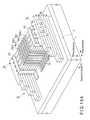
- FIG. 1is a perspective view of a nonvolatile semiconductor memory device.
- FIG. 2is a plan view of FIG. 1 .
- FIG. 3is a sectional view taken along the line III-III of FIG. 2 .
- FIG. 4is a sectional view taken along the line IV-IV of FIG. 2 .
- FIG. 5is a sectional view taken along the line V-V of FIG. 2 .
- the distances between first to fourth fin type stacked structures 9 - 1 , . . . 9 - 4 in a third directionare about four times the widths of first to fourth fin type stacked structures 9 - 1 , . . . 9 - 4 in the third direction so that a stacked gate structure is more clearly shown.
- the distances between first to fourth fin type stacked structures 9 - 1 , . . . 9 - 4 in the third direction and the widths thereof in the third directioncan be set to be equal.
- Semiconductor substrate 1is, for example, a silicon substrate.
- First, second, third, and fourth fin type stacked structures 9 - 1 , . . . 9 - 4are formed on insulating layer 1 a provided on semiconductor substrate 1 .
- Each of first to fourth fin type stacked structures 9 - 1 , . . . 9 - 4has first, second, and third memory strings 3 a (NANDa), 3 b (NANDb), and 3 c (NANDc) that are stacked in a first direction perpendicular to the surface of insulating layer 1 a on semiconductor substrate 1 .
- First to fourth fin type stacked structures 9 - 1 , . . . 9 - 4extend in a second direction parallel to the surface of insulating layer 1 a on semiconductor substrate 1 .
- First to fourth fin type stacked structures 9 - 1 , . . . 9 - 4are arranged in the third direction which is parallel to the surface of insulating layer 1 a and which is perpendicular to the first and second directions.
- first to fourth fin type stacked structures 9 - 1 , . . . 9 - 4has only to have first to i-th memory strings (i is a natural number equal to or more than 2).
- First to fourth fin type stacked structures 9 - 1 , . . . 9 - 4are connected to one another at one end in the second direction by first portion 7 a .
- First to fourth fin type stacked structures 9 - 1 , . . . 9 - 4are connected to one another at the other end in the second direction by second portion 7 b.
- Both first and second portions 7 a and 7 bhave the same stack structure as first to fourth fin type stacked structures 9 - 1 , . . . 9 - 4 .
- First to third memory strings NANDa, NANDb, and NANDc in odd fin type stacked structures 9 - 1 and 9 - 3 among first to fourth fin type stacked structures 9 - 1 , . . . 9 - 4use first portion 7 a as a drain region, and use the ends of first to third memory strings NANDa, NANDb, and NANDc on the side of second portion 7 b as a source region.
- First to third memory strings NANDa, NANDb, and NANDc in even fin type stacked structures 9 - 2 and 9 - 4 among first to fourth fin type stacked structures 9 - 1 , . . . 9 - 4use second portion 7 b as a drain region, and use the ends of first to third memory strings NANDa, NANDb, and NANDc on the side of first portion 7 a as a source region.
- first to third memory strings NANDa, NANDb, and NANDc in odd fin type stacked structures 9 - 1 and 9 - 3share first portion (drain region) 7 a .
- First to third memory strings NANDa, NANDb, and NANDc in even fin type stacked structures 9 - 2 and 9 - 4share second portion (drain region) 7 b.
- the source region of first to third memory strings NANDa, NANDb, and NANDc in odd fin type stacked structures 9 - 1 and 9 - 3is insulated from second portion (drain region) 7 b .
- the source region of first to third memory strings NANDa, NANDb, and NANDc in even fin type stacked structures 9 - 2 and 9 - 4is insulated from first portion (drain region) 7 a.
- Each of first to third memory strings NANDa, NANDb, and NANDccomprises memory cells connected in series in the second direction, a source-side select gate transistor disposed on the source side of the memory cells, a drain-side select gate transistor disposed on the drain side of the memory cells, and an assist gate transistor disposed between the drain-side select gate transistor and first portion 7 a or second portion 7 b.
- the memory cellscomprise first to third semiconductor layers 3 ( 3 a , 3 b , and 3 c ), and a stacked gate structure disposed on the side surfaces of first to third semiconductor layers 3 ( 3 a , 3 b , and 3 c ) in the third direction.
- the stacked gate structurecomprises first insulating layer 6 a , charge storage layer 6 b , second insulating layer 6 c , and electrode layer 6 d.
- First insulating layer 6 afunctions as a gate insulating layer (tunnel insulating layer).
- Second insulating layer 6 cfunctions as a block insulating layer which blocks a leak current between charge storage layer 6 b and electrode layer 6 d .
- Electrode layer 6 dfunctions as a control gate electrode, and also functions as word lines WL 1 , . . . WL 4 extending on first to fourth fin type stacked structures 9 - 1 , . . . 9 - 4 in the third direction.
- one memory stringcomprises four memory cells in this embodiment, one memory string does not exclusively comprise four memory cells.
- the number of memory cells to constitute one memory stringhas only to be k (k is a natural number equal to or more than 2) or more. In this case, the number of word lines is also k.
- the drain-side select gate transistor and the source-side select gate transistoreach comprise first to third semiconductor layers 3 ( 3 a , 3 b , and 3 c ), and a stacked gate structure disposed on the side surfaces of first to third semiconductor layers 3 ( 3 a , 3 b , and 3 c ) in the third direction.
- the stacked gate structurecomprises first insulating layer 6 a , charge storage layer 6 b , second insulating layer 6 c , and electrode layer 6 d.
- First insulating layer 6 afunctions as a gate insulating layer.
- Electrode layer 6 dfunctions as a select gate electrode, and also functions as select gate lines SGL 1 and SGL 2 extending on first to fourth fin type stacked structures 9 - 1 , . . . 9 - 4 in the third direction.
- each of these transistorsmay have a metal/insulator/semiconductor (MIS) structure that comprises a gate insulating layer and a select gate electrode disposed on the gate insulating layer.
- MISmetal/insulator/semiconductor
- the assist gate transistoralso comprises first to third semiconductor layers 3 ( 3 a , 3 b , and 3 c ), and a stacked gate structure disposed on the side surfaces of first to third semiconductor layers 3 ( 3 a , 3 b , and 3 c ) in the third direction.
- the stacked gate structurecomprises first insulating layer 6 a , charge storage layer 6 b , second insulating layer 6 c , and electrode layer 6 d.
- First insulating layer 6 afunctions as a gate insulating layer. Electrode layer 6 d functions as assist gate electrodes AG 1 , . . . AG 4 .
- the assist gate transistormay also be different in structure from the memory cells.
- the assist gate transistormay have a MIS structure that comprises a gate insulating layer and an assist gate electrode disposed on the gate insulating layer.
- Assist gate electrodes AG 1 , . . . AG 4are electrically isolated from one another. Assist gate electrodes AG 1 , . . . AG 4 are connected to assist gate lines AGL 1 , . . . AGL 4 via contact plugs AC 1 , . . . AC 4 , respectively. This allows the assist gate transistor to have a function of selecting one of first to fourth fin type stacked structures 9 - 1 , . . . 9 - 4 .
- first and second portions 7 a and 7 b in the third directionhas a staircase structure, so that the upper surfaces of first to third semiconductor layers 3 ( 3 a , 3 b , and 3 c ) are exposed.
- Parts of first to third semiconductor layers 3 ( 3 a , 3 b , and 3 c ) that expose their upper surfacesare bit line contact areas where first to third semiconductor layers 3 ( 3 a , 3 b , and 3 c ) are independently connected to bit lines BL 1 , BL 2 , and BL 3 via contact plugs BC 1 , BC 2 , and BC 3 , respectively.
- one of first to fourth fin type stacked structures 9 - 1 , . . . 9 - 4can be selected by use of the assist gate transistor, and reading/writing/erasing can be performed in first to third memory strings NANDa, NANDb, and NANDc of the selected one fin type stacked structure.
- impurity region 8is provided in first to third semiconductor layers 3 ( 3 a , 3 b , and 3 c ) of the assist gate transistor on the side of first or second portion 7 a or 7 b .
- This impurity region 8is also provided in first to third semiconductor layers 3 (including the bit line contact areas) 3 a , 3 b , and 3 c of first or second portion 7 a or 7 b.
- Impurity region (e.g., N-type diffusion layer) 8is also provided in first to third semiconductor layers 3 ( 3 a , 3 b , and 3 c ) of the assist gate transistor on the side of the memory cells.
- electrode layer 6 dhas a double gate structure that covers two sides of first to third semiconductor layers 3 ( 3 a , 3 b , and 3 c ) in the third direction in the memory cells, the drain-side select gate transistor, the source-side select gate transistor, and the assist gate transistor, the present invention is not limited to this.
- First to third memory strings NANDa, NANDb, and NANDcuse first to third semiconductor layers 3 ( 3 a , 3 b , and 3 c ) as channels.
- first to third semiconductor layers 33 a , 3 b , and 3 c ) as channels.
- increasing the number of semiconductor layers that constitutes one fin type stacked structure to increase the number of memory stringsis preferable to higher integration.
- First insulating layer 6 a , charge storage layer 6 b , second insulating layer 6 c , and electrode layer 6 dare separated in the second direction in the memory cells, the drain-side/source-side select gate transistors, and the assist gate transistor.
- first insulating layer 6 a , charge storage layer 6 b , and second insulating layer 6 cmay be united (continuous) throughout the memory cells, the drain-side/source-side select gate transistors, and the assist gate transistor.
- At least electrode layer 6 dneeds to be separated in the memory cells, the drain-side/source-side select gate transistors, and the assist gate transistor.
- the assist gate transistorsare disposed at the ends of odd fin type stacked structures 9 - 1 and 9 - 3 on the side of first portion 7 a , and disposed at the ends of even fin type stacked structures 9 - 2 and 9 - 4 on the side of second portion 7 b.
- the assist gate transistorsare alternately disposed across first to fourth fin type stacked structures 9 - 1 , . . . 9 - 4 in the third direction.
- the assist gate transistorsare alternately disposed across first to fourth fin type stacked structures 9 - 1 , . . . 9 - 4 in the third direction.
- the source region of first to third memory strings NANDa, NANDb, and NANDccomprises impurity region (e.g., N-type diffusion layer) 9 in first to third semiconductor layers 3 ( 3 a , 3 b , and 3 c ) of the memory cells on the side of first or second portion 7 a or 7 b .
- impurity region 9 as the source regionis connected to source line SL via contact plug SC.
- the source region of first to third memory strings NANDa, NANDb, and NANDcis disposed closer to the memory cells than a line that connects assist gate electrodes AG 1 , . . . AG 4 in the third direction.
- damagemay be caused to first to third semiconductor layers 3 ( 3 a , 3 b , and 3 c ) in second and fourth fin type stacked structures 9 - 2 and 9 - 4 adjacent to assist gate electrodes AG 1 and AG 3 in the third direction, and to first to third semiconductor layers 3 ( 3 a , 3 b , and 3 c ) in first and third stack structures 9 - 1 and 9 - 3 adjacent to assist gate electrodes AG 2 and AG 4 in the third direction.
- damageis out of channel paths (current paths) of first to third memory strings NANDa, NANDb, and NANDc and has no adverse effect on the read/write/erase operation.
- first to fourth fin type stacked structures 9 - 1 , . . . 9 - 4is drain D, and the other end thereof is drain D, and the other end thereof is source S.
- Assist gate electrodes AG 1 , . . . AG 4are collectively disposed at one end (drain D) of first to fourth fin type stacked structures 9 - 1 , . . . 9 - 4 , and are aligned in the third direction.
- the space between assist gate electrodes AG 1 , . . . AG 4should be set at size W 1 sufficient to pattern the assist gate electrodes. Accordingly, space W 2 between first to fourth fin type stacked structures 9 - 1 , . . . 9 - 4 also increases.
- first to fourth fin type stacked structures 9 - 1 , . . . 9 - 4is drain D, and the other end thereof is drain D, and the other end thereof is drain D.
- Assist gate electrodes AG 1 , . . . AG 4are collectively disposed at one end (drain D) of first to fourth fin type stacked structures 9 - 1 , . . . 9 - 4 .
- assist gate electrodes AG 1 and AG 3 and assist gate electrodes AG 2 and AG 4are shifted a predetermined distance in the second direction. That is, assist gate electrodes AG 1 , . . . AG 4 are arranged in the form of a zigzag pattern in the third direction.
- space W 3 between assist gate electrodes AG 1 and AG 3can be greater, and space W 3 between assist gate electrodes AG 2 and AG 4 can be greater. This makes it possible to decrease space W 4 between first to fourth fin type stacked structures 9 - 1 , . . . 9 - 4 and contribute to higher integration.
- odd fin type stacked structures 9 - 1 and 9 - 3the side of first portion 7 a is drain D, and the side of second portion 7 b is source S.
- even fin type stacked structures 9 - 2 and 9 - 4the side of second portion 7 b is drain D, and the side of first portion 7 a is source S. That is, the relation between drain D and source S of odd fin type stacked structures 9 - 1 and 9 - 3 is opposite to that of even fin type stacked structures 9 - 2 and 9 - 4 .
- Source Sis disposed closer to the memory cells than the line that connects assist gate electrodes AG 1 , . . . AG 4 in the third direction.
- space W 3 between assist gate electrodes AG 1 and AG 3can be greater, and space W 3 between assist gate electrodes AG 2 and AG 4 can be greater. This makes it possible to decrease space W 4 between first to fourth fin type stacked structures 9 - 1 , . . . 9 - 4 and contribute to higher integration.
- the damage (defects in the semiconductor layers) caused in first to fourth fin type stacked structures 9 - 1 , . . . 9 - 4increases the parasitic resistance of the channel of the memory string, and therefore reduces the current running through the channel during reading/writing and reduces the reading/writing speed.
- this problemdoes not occur if the damage is outside the channel path of the memory string.
- Materials best suited to the generations of semiconductor memoriescan be properly selected as the materials that constitute the elements of the device structure shown in FIG. 1 to FIG. 5 .
- first insulating layer 2is made of silicon oxide (SiO 2 ).
- First to third semiconductor layers 3are made of, for example, monocrystalline silicon (Si).
- First to third semiconductor layers 3are preferably monocrystalline, but may be amorphous or polycrystalline.
- Second and third insulating layers 4are made of, for example, silicon oxide (SiO 2 ).
- Fourth insulating layer 5is made of, for example, silicon oxide (SiO 2 ), silicon nitride (SiN X ), or a structure in which these materials are stacked.
- Each of first to third memory strings NANDa, NANDb, and NANDchas a silicon/oxide/nitride/oxide/silicon (SONGS) structure.
- SONGSsilicon/oxide/nitride/oxide/silicon
- First gate insulating layer 6 acan be made of SiO 2
- charge storage layer 6 bcan be made of Si 3 N 4
- second gate insulating layer 6 ccan be made of Al 2 O 3
- control gate electrode 6 dcan be made of NiSi.
- First gate insulating layer 6 amay be, for example, silicon oxynitride, or a stack structure of silicon oxide and silicon nitride. First gate insulating layer 6 a may also include, for example, silicon nanoparticles, or metal ions.
- Charge storage layer 6 bcan be made of at least one of the materials selected from the group consisting of silicon-rich SiN, Si x N y having any composition ratio x, y of silicon and nitrogen, silicon oxynitride (SiON), aluminum oxide (Al 2 O 3 ), aluminum oxynitride (AlON), hafnia (HfO 2 ), hafnium aluminate (HfAlO 3 ), hafnia oxynitride (HfON), hafnium nitride-aluminate (HfAlON), hafnium silicate (HfSiO), hafnium nitride-silicate (HfSiON), lanthanum oxide (La 2 O 3 ), and lanthanum aluminate (LaAlO 3 ).
- Charge storage layer 6 bmay include silicon nanoparticles or metal ions. Charge storage layer 6 b may otherwise be made of impurity-added polysilicon or a conductor such as a metal.
- Second gate insulating layer 6 ccan be made of at least one of the materials selected from the group consisting of silicon oxide (SiO 2 ), silicon oxynitride (SiON), aluminum oxide (Al 2 O 3 ), aluminum oxynitride (AlON), hafnia (HfO 2 ), hafnium aluminate (HfAlO 3 ), hafnia oxynitride (HfON), hafnium nitride-aluminate (HfAlON), hafnium silicate (HfSiO), hafnium nitride-silicate (HfSiON), lanthanum oxide (La 2 O 3 ), lanthanum aluminate (LaAlO 3 ), and lanthanum aluminum silicate (LaAlSiO).
- Electrode layer 6 dcan be made of a metal compound such as tantalum nitride (TaN), tantalum carbide (TaC), or titanium nitride (TiN), or an electrically conductive metallic material such as Ni, V, Cr, Mn, Y, Mo, Ru, Rh, Hf, Ta, W, Ir, Co, Ti, Er, Pt, Pd, Zr, Gd, Dy, Ho, Er and silicides of these substances.
- a metal compoundsuch as tantalum nitride (TaN), tantalum carbide (TaC), or titanium nitride (TiN)
- an electrically conductive metallic materialsuch as Ni, V, Cr, Mn, Y, Mo, Ru, Rh, Hf, Ta, W, Ir, Co, Ti, Er, Pt, Pd, Zr, Gd, Dy, Ho, Er and silicides of these substances.
- an impurity serving as an N-type semiconductorfor example, a pentad such as arsenic (As) or phosphorus (P), an impurity serving as a P-type semiconductor, for example, a triad such as boron (B) or indium (In), and a combination of these substances.
- a pentadsuch as arsenic (As) or phosphorus (P)
- an impurity serving as a P-type semiconductorfor example, a triad such as boron (B) or indium (In)
- Contact plugs BC 1 , BC 2 , BC 3 , AC 1 , . . . AC 4 , and SC, bit lines BL 1 , BL 2 , and BL 3 , assist gate lines AGL 1 , . . . AGL 4 , and source line SLcan be made of, for example, a metal material such as W or Al.
- Contact plugs BC 1 , BC 2 , BC 3 , AC 1 , . . . AC 4 , and SC, bit lines BL 1 , BL 2 , and BL 3 , assist gate lines AGL 1 , . . . AGL 4 , and source line SLcan be made of the same material or different materials.
- Bit lines BL 1 , BL 2 , and BL 3 , and assist gate lines AGL 1 , . . . AGL 4can be formed in the same wiring layer, and are therefore preferably made of the same material.
- FIG. 6shows a first modification of the device structure shown in FIG. 1 to FIG. 5 .
- This modificationis characterized in that bit line contact areas with the staircase structure are provided at the ends of first and second portions 7 a and 7 b in the second direction.
- the distance between contact plugs BC 1 , BC 2 , and BC 3 and all fin type stacked structurescan be equal by adjusting the sizes and number of contact plugs BC 1 , BC 2 , and BC 3 . This can reduce characteristic variations among the fin type stacked structures in the read/write/erase operation.
- FIG. 7shows a second modification of the device structure shown in FIG. 1 to FIG. 5 .
- This modificationis characterized in that a source (contact plug SC) is positioned closer to first or second portion 7 a or 7 b than the line that connects assist gate electrodes AG 1 , . . . AG 4 in the third direction.
- a sourcecontact plug SC
- damagemay be caused to the channel path (current path) of the memory string.
- damage in the semiconductor layerscan be reduced by the enhancement of an etching technique or by the enhancement of process technology in, for example, a post-etching treatment, the structure shown in the second modification can be sufficiently practically used.
- FIG. 8shows a third modification of the device structure shown in FIG. 1 to FIG. 5 .
- This modificationis characterized in that a source (contact plug SC) is positioned on the line that connects assist gate electrodes AG 1 , . . . AG 4 in the third direction.
- contact plug SCpierces first to third semiconductor layers 3 ( 3 a , 3 b , and 3 c ). That is, when a contact hole for forming contact plug SC is made, the damage caused in the channel path (current path) of the memory string is removed.
- FIG. 9shows a memory cell array that uses the device structure shown in FIG. 1 to FIG. 5 .
- m assist gate lines AGL 1 , . . . AGLmcorrespond to the m fin type stacked structures.
- first and second portions 7 a and 7 b in the third directionhas a staircase structure
- bit line contact areasare provided at both ends of first and second portions 7 a and 7 b in the third direction.
- first and second portions 7 a and 7 bcan have the staircase structure at one end only in the third direction, and bit line contact areas can be provided at these ends.
- a group including fin type stacked structures arranged in the third directionis defined as one block.
- two blocks BK 1 and BK 2are shown.
- m fin type stacked structures in block BK 1are connected to bit lines BL 1 , BL 2 , and BL 3 , respectively.
- m fin type stacked structures in block BK 2are connected to bit lines BL 4 , BL 5 , and BL 6 , respectively.
- m assist gate lines AGL 1 , . . . AGLmare provided in two common blocks BK 1 and BK 2 .
- reading/writing/erasingcan be simultaneously performed in one selected fin type stacked structure within block BK 1 and in one selected fin type stacked structure within block BK 2 .
- the number of memory strings in one blockis (the number of memory strings in one fin type stacked structure) ⁇ (the number of columns m). Therefore, a three-dimensionally stacked semiconductor memory having a high memory capacity can be obtained.
- FIG. 1 to FIG. 9An example of the operation of the nonvolatile semiconductor memory device of the first embodiment ( FIG. 1 to FIG. 9 ) is described.
- a ground potentialis applied to bit lines BL 1 , BL 2 , and BL 3 and source line SL, and in this condition, a first positive bias is applied to all word lines WL 1 , . . . WL 4 .
- N-type impurity storage regionsare formed in first to third semiconductor layers 3 a , 3 b , and 3 c serving as channels of first to third memory strings NANDa, NANDb, and NANDc.
- assist gate line AGL 1is set to, for example, “H”, and the assist gate transistor in first fin type stacked structure 9 - 1 is switched on.
- the assist gate transistors in second to fourth fin type stacked structures 9 - 2 , . . . 9 - 4are off.
- His defined as a potential for switching on the transistor
- Lis defined as a potential for switching off the transistor. The same applies to the following cases.
- a second positive bias higher than the first positive biasis applied to word line (control gate electrode) WL-select of the selected memory cell targeted for writing, and program data “0”/“1” is transferred to the channels of first to third memory strings NANDa, NANDb, and NANDc in first fin type stacked structure 9 - 1 from bit lines BL 1 , BL 2 , and BL 3 .
- first to third memory strings NANDa, NANDb, and NANDc in second to fourth fin type stacked structures 9 - 2 , . . . 9 - 4the channel potential is increased by capacitive coupling resulting from the application of the second positive bias. Therefore, a voltage high enough for writing is not applied across the control gate electrode (or charge storage layer) and the channel, and writing is inhibited accordingly.
- first to third memory strings NANDa, NANDb, and NANDc in first fin type stacked structure 9 - 1the assist gate transistors are on, so that program data “0”/“1” is transferred to first to third semiconductor layers 3 a , 3 b , and 3 c as the channels.
- the channelfor example, has a positive potential.
- the drain-side select gate transistoris cut off when the channel potential is slightly increased by the capacitive coupling.
- the channel potentialis increased by the capacitive coupling resulting from the application of the second positive bias. That is, a voltage high enough for writing is not applied across the control gate electrode (or charge storage layer) and the channel, and electrons are not injected into the charge storage layer. That is, writing is inhibited (“0”-programming).
- the channelfor example, has a ground potential. In this condition, even if the second positive bias is applied to the control gate electrode of the selected memory cell, the drain-side select gate transistor is not cut off.
- the erase operationcan be simultaneously performed in, for example, first to third memory strings NANDa, NANDb, and NANDc in selected one or more fin type stacked structures.
- a ground potentialis applied to bit lines BL 1 , BL 2 , and BL 3 and source line SL, and a first negative bias is applied to select gate lines SGL 1 and SGL 2 and word lines WL 1 , . . . WL 4 .
- P-type impurity storage regionsare formed in first to third semiconductor layers 3 a , 3 b , and 3 c serving as channels of first to third memory strings NANDa, NANDb, and NANDc.
- the potential of the assist gate line corresponding to selected one or more fin type stacked structures targeted for erasingis set to “H”, and the assist gate transistor corresponding to selected one or more fin type stacked structures is switched on.
- a second negative bias higher than the first negative biasis then applied to all word lines WL 1 , . . . WL 4 .
- a reading circuitis connected to bit lines BL 1 , BL 2 , and BL 3 , and a ground voltage is applied to source line SL.
- the potential of assist gate line AGL 1is set to, for example, “H”, and the assist gate transistor in first fin type stacked structure 9 - 1 is switched on.
- the assist gate transistors in second to fourth fin type stacked structures 9 - 2 , . . . 9 - 4are off.
- a first positive biasis applied to select gate lines SGL 1 and SGL 2 and word lines WL 1 , . . . WL 4 .
- the first positive biashas a value that the memory cells turn on regardless of whether data in the memory cells is “0” or “1”.
- datais sequentially read in first to third memory strings NANDa, NANDb, and NANDc from the memory cells on the source region side to the memory cells on the drain region side.
- a second positive bias for reading lower than the first positive biasis applied to the control gate electrode.
- the second positive biashas, for example, a value between the threshold of the “0”-data and the threshold of the “1”-data.
- whether to switch on or off the selected memory cellis determined by the value of the data stored in the selected memory cell, so that reading can be performed by using the reading circuit to detect potential changes in bit lines BL 1 , BL 2 , and BL 3 and changes in currents running through bit lines BL 1 , BL 2 , and BL 3 .
- FIG. 10A to FIG. 10Dshow a method of manufacturing the structure shown in FIG. 1 to FIG. 9 .
- bit line contact area 10 with a staircase structurebit line contact area 10 with a staircase structure, first to fourth fin type stacked structures 9 - 1 , . . . 9 - 4 , and first and second portions 7 a and 7 b are formed.
- Bit line contact area 10is formed, for example, as follows.
- first-conductivity-type (e.g., P-type) semiconductor substrate (e.g., silicon) 1 having, for example, a plane direction ( 100 ) and a specific resistance of 10 to 20 ⁇ cmis prepared.
- element isolation insulating layer 1 a and first insulating layer 2are formed, and first semiconductor layer (e.g., silicon) 3 a is formed on first insulating layer 2 .
- a resist patternis then formed on first semiconductor layer 3 a by a photo engraving process (PEP). Ions are implanted using this resist pattern as a mask, thereby forming an impurity region in first semiconductor layer 3 a . The resist pattern is removed afterwards.
- PEPphoto engraving process
- a resist patternis again formed on first semiconductor layer 3 a by the PEP.
- Reactive ion etchingRIE
- RIEreactive ion etching
- Second insulating layer 4 a and second semiconductor layer 3 bare then formed on first semiconductor layer 3 a .
- a resist patternis then formed on second semiconductor layer 3 b by the PEP. Ions are implanted using this resist pattern as a mask, thereby forming an impurity region in second semiconductor layer 3 b . The resist pattern is removed afterwards.
- a resist patternis again formed on second semiconductor layer 3 b by the PEP.
- the RIEis performed using this resist pattern as a mask, thereby patterning second semiconductor layer 3 b and second insulating layer 4 a .
- the resist patternis removed afterwards.
- Third insulating layer 4 b and third semiconductor layer 3 care then formed on second semiconductor layer 3 b .
- a resist patternis then formed on third semiconductor layer 3 c by the PEP. Ions are implanted using this resist pattern as a mask, thereby forming an impurity region in third semiconductor layer 3 c .
- the resist patternis removed afterwards.
- a resist patternis again formed on third semiconductor layer 3 c by the PEP.
- the RIEis performed using this resist pattern as a mask, thereby patterning third semiconductor layer 3 c and third insulating layer 4 b .
- the resist patternis removed afterwards.
- fourth insulating layer 5is formed on third semiconductor layer 3 c .
- a resist patternis formed on fourth insulating layer 5 by the PEP. The RIE is performed using this resist pattern as a mask, thereby patterning fourth insulating layer 5 . The resist pattern is removed afterwards.
- bit line contact area 10 with a staircase structureis formed at the end in the third direction.
- a resist patternis formed on fourth insulating layer 5 by the PEP.
- the RIEis performed using this resist pattern as a mask, thereby patterning fourth insulating layer 5 , third semiconductor layer 3 c , third insulating layer 4 b , second semiconductor layer 3 b , second insulating layer 4 a , first semiconductor layer 3 a , and first insulating layer 2 .
- first to fourth fin type stacked structures 9 - 1 , . . . 9 - 4 , and first and second portions 7 a and 7 bare formed on element isolation insulating layer 1 a on semiconductor substrate 1 .
- the resist patternis removed afterwards.
- the stacked gate structurecomprises, for example, a first insulating layer, a charge storage layer, a second insulating layer, and an electrode layer.
- a resist patternis again formed on this stacked gate structure.
- the RIEis performed using this resist pattern as a mask, thereby forming word lines WL 1 , . . . WL 4 , select gate lines SGL 1 and SGL 2 , and assist gate electrode AG.
- the resist patternis removed afterwards.
- assist gate electrode AGis disposed across first to fourth fin type stacked structures 9 - 1 , . . . 9 - 4 .
- a resist patternis again formed on the stacked gate structure.
- This resist patternis used as a mask to etch assist gate electrode AG in FIG. 10B , such that assist gate electrodes AG 1 , . . . AG 4 of first to fourth fin type stacked structures 9 - 1 , . . . 9 - 4 are electrically isolated from one another.
- the resist patternis removed afterwards.
- assist gate electrodes AG 1 , . . . AG 4are patterned by two etchings in this embodiment, assist gate electrodes AG 1 , . . . AG 4 of first to fourth fin type stacked structures 9 - 1 , . . . 9 - 4 can be electrically isolated from one another, for example, by one etching in the process in FIG. 10B .
- the base for this processcan be planarized by chemical mechanical processing (CMP).
- CMPchemical mechanical processing
- an insulating film of, for example, SiO 2may be deposited before the CMP.
- contact plugs BC 1 , BC 2 , and BC 3are formed on first to third semiconductor layers 3 a , 3 b , and 3 c in bit line contact area 10
- contact plugs AC 1 , . . . AC 4are formed on assist gate electrodes AG 1 , . . . AG 4
- contact plug SCis formed on the source region.
- bit lines BL 1 , BL 2 , and BL 3are formed on contact plugs BC 1 , BC 2 , and BC 3
- assist gate lines AGL 2 , . . . AGL 4are formed on contact plugs AC 1 , . . . AC 4
- source line SLis formed on contact plug SC.
- FIG. 1 to FIG. 9The structure shown in FIG. 1 to FIG. 9 is completed in the process described above.
- adjacent two fin type stacked structuresare combined together by the first and second portions.
- One of the two fin type stacked structuresuses the first portion as the drain region, and the other fin type stacked structure uses the second portion as the drain region. That is, the even fin type stacked structure and the odd fin type stacked structure are different in the direction of the memory string (the relation between the source region and the drain region).
- the assist gate electrodesit is thus possible to increase the pitch of the assist gate electrodes and reduce the pitch of the fin type stacked structures, and achieve higher integration of the nonvolatile semiconductor memory device. As the processing of the assist gate electrodes is facilitated, it is also possible to contribute to higher reliability. Moreover, the source region of one of the two fin type stacked structures is located at the same position as the assist gate electrode of the other of the two fin type stacked structures or located closer to the memory cells, so that reliability is further enhanced.
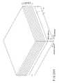
- FIG. 11is a perspective view of a nonvolatile semiconductor memory device.
- FIG. 12is a plan view of the device of FIG. 11 .
- FIG. 13is a sectional view taken along the line XIII-XIII of FIG. 12 .
- FIG. 14is a sectional view taken along the line XIV-XIV of FIG. 12 .
- FIG. 15is a sectional view taken along the line XV-XV of FIG. 12 .
- the distances between first to fourth fin type stacked structures 9 - 1 , . . . 9 - 4 in a third directionare about four times the widths of first to fourth fin type stacked structures 9 - 1 , . . . 9 - 4 in the third direction so that a stacked gate structure is more clearly shown.
- the distances between first to fourth fin type stacked structures 9 - 1 , . . . 9 - 4 in the third direction and the widths thereof in the third directioncan be set to be equal.
- the structure of the second embodiment( FIG. 11 to FIG. 15 ) is a modification of the structure of the first embodiment ( FIG. 1 to FIG. 5 ).
- the same elements as those in the first embodimentare provided with the same signs and are not described in detail.
- the structure of the second embodimentis characterized in that odd fin type stacked structures 9 - 1 and 9 - 3 are apart from second portion 7 b at the other end in a second direction and even fin type stacked structures 9 - 2 and 9 - 4 are apart from first portion 7 a at the other end in the second direction.
- even fin type stacked structures 9 - 2 and 9 - 4are not present on a line that connects assist gate electrodes AG 1 and AG 3 in odd fin type stacked structures 9 - 1 and 9 - 3 .
- odd fin type stacked structures 9 - 1 and 9 - 3are not present on a line that connects assist gate electrodes AG 2 and AG 4 in even fin type stacked structures 9 - 2 and 9 - 4 .
- the source region at the other end of odd fin type stacked structures 9 - 1 and 9 - 3 in the second directioncan be completely insulated from second portion 7 b which is the drain region of even fin type stacked structures 9 - 2 and 9 - 4 . It is thus possible to prevent the generation of an unintended current path (leak current) between the source region and the drain region.
- the source region at the other end of even fin type stacked structures 9 - 2 and 9 - 4 in the second directioncan be completely insulated from first portion 7 a which is the drain region of odd fin type stacked structures 9 - 1 and 9 - 3 . It is thus possible to prevent the generation of an unintended current path (leak current) between the source region and the drain region.
- Materials best suited to the generations of semiconductor memoriescan be properly selected as the materials that constitute the elements of the device structure shown in FIG. 11 to FIG. 15 .
- FIG. 16shows a modification of the device structure shown in FIG. 11 to FIG. 15 .
- the same elements as those in FIG. 11 to FIG. 15are provided with the same signs and are not described in detail.
- This modificationis characterized in that bit line contact areas with a staircase structures are provided at the ends of first and second portions 7 a and 7 b in the second direction.
- the distance between contact plugs BC 1 , BC 2 , and BC 3 and all fin type stacked structurescan be equal by adjusting the sizes and number of contact plugs BC 1 , BC 2 , and BC 3 . This can reduce characteristic variations among the fin type stacked structures in the read/write/erase operation.
- FIG. 17shows a memory cell array that uses the device structure shown in FIG. 11 to FIG. 15 .
- the same elements as those in FIG. 11 to FIG. 15are provided with the same signs and are not described in detail.
- m assist gate lines AGL 1 , . . . AGLmcorrespond to the m fin type stacked structures.
- first and second portions 7 a and 7 b in the third directionhave staircase structures
- bit line contact areasare provided at both ends of first and second portions 7 a and 7 b in the third direction.
- first and second portions 7 a and 7 bcan have a staircase structure at one end only in the third direction, and bit line contact areas can be provided at these ends.
- a group including fin type stacked structures arranged in the third directionis defined as one block.
- two blocks BK 1 and BK 2are shown.
- m fin type stacked structures in block BK 1are connected to bit lines BL 1 , BL 2 , and BL 3 , respectively.
- m fin type stacked structures in block BK 2are connected to bit lines BL 4 , BL 5 , and BL 6 , respectively.
- m assist gate lines AGL 1 , . . . AGLmare provided in two common blocks BK 1 and BK 2 .
- reading/writing/erasingcan be simultaneously performed in one selected fin type stacked structure within block BK 1 and in one selected fin type stacked structure within block BK 2 .
- the number of memory strings in one blockis (the number of memory strings in one fin type stacked structure) ⁇ (the number of columns m). Therefore, a three-dimensionally stacked semiconductor memory having a high memory capacity can be obtained.
- the operation of the nonvolatile semiconductor memory device of the second embodiment( FIG. 11 to FIG. 19 ) is the same as that in the first embodiment, and is therefore not described here.
- FIG. 18A to FIG. 18Cshow a method of manufacturing the structure shown in FIG. 11 to FIG. 17 .
- bit line contact area 10 with a staircase structurebit line contact area 10 with a staircase structure, first to fourth fin type stacked structures 9 - 1 , . . . 9 - 4 , and first and second portions 7 a and 7 b are formed.
- Bit line contact area 10can be manufactured, for example, in the same process as that in the first embodiment, and is therefore not described here. Consequently, a stack structure including bit line contact area 10 is formed.
- the stack structure including bit line contact area 10comprises semiconductor substrate 1 , element isolation insulating layer 1 a on semiconductor substrate 1 and first insulating layer 2 , first semiconductor layer 3 a on first insulating layer 2 , second insulating layer 4 a on first semiconductor layer 3 a , second semiconductor layer 3 b on second insulating layer 4 a , third insulating layer 4 b on second semiconductor layer 3 b , third semiconductor layer 3 c on third insulating layer 4 b , and fourth insulating layer 5 on third semiconductor layer 3 c.
- the stack structure including bit line contact area 10is then patterned, thereby forming first to fourth fin type stacked structures 9 - 1 , . . . 9 - 4 , and first and second portions 7 a and 7 b.
- a resist patternis formed on fourth insulating layer 5 by the PEP.
- the RIEis performed using this resist pattern as a mask, thereby patterning fourth insulating layer 5 , third semiconductor layer 3 c , third insulating layer 4 b , second semiconductor layer 3 b , second insulating layer 4 a , first semiconductor layer 3 a , and first insulating layer 2 .
- first to fourth fin type stacked structures 9 - 1 , . . . 9 - 4 , and first and second portions 7 a and 7 bare formed on element isolation insulating layer 1 a on semiconductor substrate 1 .
- the resist patternis removed afterwards.
- the stacked gate structurecomprises, for example, a first insulating layer, a charge storage layer, a second insulating layer, and an electrode layer.
- a resist patternis formed on this stacked gate structure.
- the RIEis performed using this resist pattern as a mask, thereby forming word lines WL 1 , . . . WL 4 , select gate lines SGL 1 and SGL 2 , and assist gate electrode AG.
- the resist patternis removed afterwards.
- assist gate electrode AGis disposed across first to fourth fin type stacked structures 9 - 1 , . . . 9 - 4 .
- a resist patternis again formed on the stacked gate structure.
- This resist patternis used as a mask to etch assist gate electrode AG in FIG. 18A , such that assist gate electrodes AG 1 , . . . AG 4 of first to fourth fin type stacked structures 9 - 1 , . . . 9 - 4 are electrically isolated from one another.
- odd fin type stacked structures 9 - 1 and 9 - 3 among first to fourth fin type stacked structures 9 - 1 , . . . 9 - 4are cut from second portion 7 b at the other end in the second direction
- even fin type stacked structures 9 - 2 and 9 - 4 among first to fourth fin type stacked structures 9 - 1 , . . . 9 - 4are cut from first portion 7 a at the other end in the second direction.
- the resist patternis removed afterwards.
- assist gate electrodes AG 1 , . . . AG 4are patterned by two etchings. However, for example, by one etching in the process in FIG. 18A , assist gate electrodes AG 1 , . . . AG 4 of first to fourth fin type stacked structures 9 - 1 , . . . 9 - 4 can be electrically isolated from one another, and first to fourth fin type stacked structures 9 - 1 , . . . 9 - 4 can be cut at the other end in the second direction.
- the base for this processcan be planarized by the CMP.
- contact plugs BC 1 , BC 2 , and BC 3are formed on first to third semiconductor layers 3 a , 3 b , and 3 c in bit line contact area 10
- contact plugs AC 1 , . . . AC 4are formed on assist gate electrodes AG 1 , . . . AG 4
- contact plug SCis formed on the source region.
- bit lines BL 1 , BL 2 , and BL 3are formed on contact plugs BC 1 , BC 2 , and BC 3
- assist gate lines AGL 1 , . . . AGL 4are formed on contact plugs AC 1 , . . . AC 4
- source line SLis formed on contact plug SC.
- FIG. 11 to FIG. 17The structure shown in FIG. 11 to FIG. 17 is completed in the process described above.
- odd fin type stacked structuresare apart from the second portion (the drain region of the even fin type stacked structures) at the other end (source region) in the second direction
- even fin type stacked structuresare apart from the first portion (the drain region of the odd fin type stacked structures) at the other end (source region) in the second direction.
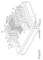
- FIG. 19is a perspective view of a nonvolatile semiconductor memory device.
- FIG. 20is a plan view of the device of FIG. 19 .
- FIG. 21is a sectional view taken along the line XXI-XXI of FIG. 20 .
- the third embodimentis a modification of the first and second embodiments. That is, the third embodiment uses the first or second embodiment as the basic structure, and modifies part of this basic structure. While the second embodiment is used as the basic structure in the example described below to prevent repeated explanations, it should be understood that the first embodiment can also be used as the basic structure.
- Semiconductor substrate 1is, for example, a silicon substrate.
- First, second, third, and fourth fin type stacked structures 9 - 1 , . . . 9 - 4are formed on insulating layer 1 a provided on semiconductor substrate 1 .
- Each of first to fourth fin type stacked structures 9 - 1 , . . . 9 - 4has first, second, and third memory strings 3 a (NANDa), 3 b (NANDb), and 3 c (NANDc) that are stacked in a first direction perpendicular to the surface of insulating layer 1 a on semiconductor substrate 1 .
- First to fourth fin type stacked structures 9 - 1 , . . . 9 - 4extend in a second direction parallel to the surface of insulating layer 1 a on semiconductor substrate 1 .
- First to fourth fin type stacked structures 9 - 1 , . . . 9 - 4are arranged in a third direction which is parallel to the surface of insulating layer 1 a and which is perpendicular to the first and second directions.
- first to fourth fin type stacked structures 9 - 1 , . . . 9 - 4has only to have first to i-th memory strings (i is a natural number equal to or more than 2).
- Odd fin type stacked structures 9 - 1 and 9 - 3 among first to fourth fin type stacked structures 9 - 1 , . . . 9 - 4are connected to each other by first portion 7 a at one end in the second direction. Odd fin type stacked structures 9 - 1 and 9 - 3 are apart from second portion 7 b at the other end in the second direction.
- fin type stacked structures 9 - 2 and 9 - 4 among first to fourth fin type stacked structures 9 - 1 , . . . 9 - 4are connected to each other by second portion 7 b at one end in the second direction. Even fin type stacked structures 9 - 2 and 9 - 4 are apart from first portion 7 a at the other end in the second direction.
- Both first and second portions 7 a and 7 bhave the same stack structure as first to fourth fin type stacked structures 9 - 1 , . . . 9 - 4 .
- First portion 7 ahas, at its end in the third direction, first common semiconductor 14 which connects first to third memory strings NANDa, NANDb, and NANDc in odd fin type stacked structures 9 - 1 and 9 - 3 to one another, and contact plug (drain electrode) BC 1 connected to first common semiconductor 14 .
- second portion 7 bhas, at its end in the third direction, second common semiconductor 14 which connects first to third memory strings NANDa, NANDb, and NANDc in even fin type stacked structures 9 - 2 and 9 - 4 to one another, and contact plug (drain electrode) BC 1 connected to first common semiconductor 14 .
- First to third memory strings NANDa, NANDb, and NANDc in odd fin type stacked structures 9 - 1 and 9 - 3use first portion 7 a as a drain region, and use the ends of first to third memory strings NANDa, NANDb, and NANDc on the side of second portion 7 b as a source region.
- First to third memory strings NANDa, NANDb, and NANDc in even fin type stacked structures 9 - 2 and 9 - 4use second portion 7 b as a drain region, and use the ends of first to third memory strings NANDa, NANDb, and NANDc on the side of first portion 7 a as a source region.
- first to third memory strings NANDa, NANDb, and NANDc in odd fin type stacked structures 9 - 1 and 9 - 3share first portion (drain region) 7 a .
- First to third memory strings NANDa, NANDb, and NANDc in even fin type stacked structures 9 - 2 and 9 - 4share second portion (drain region) 7 b.
- the source region of first to third memory strings NANDa, NANDb, and NANDc in odd fin type stacked structures 9 - 1 and 9 - 3is insulated from second portion (drain region) 7 b .
- the source region of first to third memory strings NANDa, NANDb, and NANDc in even fin type stacked structures 9 - 2 and 9 - 4is insulated from first portion (drain region) 7 a.
- Each of first to third memory strings NANDa, NANDb, and NANDccomprises memory cells connected in series in the second direction, a source-side select gate transistor disposed on the source side of the memory cells, a drain-side select gate transistor disposed on the drain side of the memory cells, and an assist gate transistor disposed between the drain-side select gate transistor and first portion 7 a or second portion 7 b.
- the memory cellscomprise first to third semiconductor layers 3 ( 3 a , 3 b , and 3 c ), and a stacked gate structure disposed on the side surfaces of first to third semiconductor layers 3 ( 3 a , 3 b , and 3 c ) in the third direction.
- the stacked gate structurecomprises first insulating layer 6 a , charge storage layer 6 b , second insulating layer 6 c , and electrode layer 6 d.
- First insulating layer 6 afunctions as a gate insulating layer (tunnel insulating layer).
- Second insulating layer 6 cfunctions as a block insulating layer which blocks a leak current between charge storage layer 6 b and electrode layer 6 d .
- Electrode layer 6 dfunctions as a control gate electrode, and also functions as word lines WL 1 , . . . WL 4 extending on first to fourth fin type stacked structures 9 - 1 , . . . 9 - 4 in the third direction.
- one memory stringcomprises four memory cells in this embodiment, one memory string does not exclusively comprise four memory cells.
- the number of memory cells to constitute one memory stringhas only to be k (k is a natural number equal to or more than 2) or more. In this case, the number of word lines is also k.
- the drain-side select gate transistor and the source-side select gate transistoreach comprise first to third semiconductor layers 3 ( 3 a , 3 b , and 3 c ), and a stacked gate structure disposed on the side surfaces of first to third semiconductor layers 3 ( 3 a , 3 b , and 3 c ) in the third direction.
- the stacked gate structurecomprises first insulating layer 6 a , charge storage layer 6 b , second insulating layer 6 c , and electrode layer 6 d.
- First insulating layer 6 afunctions as a gate insulating layer.
- Electrode layer 6 dfunctions as a select gate electrode, and also functions as select gate lines SGL 1 and SGL 2 extending on first to fourth fin type stacked structures 9 - 1 , . . . 9 - 4 in the third direction.
- each of these transistorsmay have a MIS structure that comprises a gate insulating layer and a select gate electrode disposed on the gate insulating layer.
- the drain-side select gate transistorcan be normally on. This is because first to third layer select transistors are provided in first and second portions 7 a and 7 b . The first to third layer select transistors will be described later.
- the assist gate transistoralso comprises first to third semiconductor layers 3 ( 3 a , 3 b , and 3 c ), and a stacked gate structure disposed on the side surfaces of first to third semiconductor layers 3 ( 3 a , 3 b , and 3 c ) in the third direction.
- the stacked gate structurecomprises first insulating layer 6 a , charge storage layer 6 b , second insulating layer 6 c , and electrode layer 6 d.
- First insulating layer 6 afunctions as a gate insulating layer. Electrode layer 6 d functions as assist gate electrodes AG 1 , . . . AG 4 .
- the assist gate transistormay also be different in structure from the memory cells.
- the assist gate transistormay have a MIS structure that comprises a gate insulating layer and an assist gate electrode disposed on the gate insulating layer.
- Assist gate electrodes AG 1 , . . . AG 4are electrically isolated from one another. Assist gate electrodes AG 1 , . . . AG 4 are connected to assist gate lines AGL 1 , . . . AGL 4 via contact plugs AC 1 , . . . AC 4 , respectively. This allows the assist gate transistor to have a function of selecting one of first to fourth fin type stacked structures 9 - 1 , . . . 9 - 4 .
- first to third layer select transistorsare formed, for example, at the ends of first and second portions 7 a and 7 b in the third direction, so that one of first to third memory strings NANDa, NANDb, and NANDc can be selected.
- one of first to fourth fin type stacked structures 9 - 1 , . . . 9 - 4can be further selected by using the assist gate transistor. Reading/writing/erasing can be performed in the selected one memory string in the selected one fin type stacked structure.
- impurity region 8is provided in first to third semiconductor layers 3 ( 3 a , 3 b , and 3 c ) of the assist gate transistor on the side of first or second portion 7 a or 7 b .
- This impurity region 8is also provided in first to third semiconductor layers 3 (including the bit line contact areas) 3 a , 3 b , and 3 c of first or second portion 7 a or 7 b.
- Impurity region (e.g., N-type diffusion layer) 8is also provided in first to third semiconductor layers 3 ( 3 a , 3 b , and 3 c ) of the assist gate transistor on the side of the memory cells.
- electrode layer 6 dhas a double gate structure that covers two sides of first to third semiconductor layers 3 ( 3 a , 3 b , and 3 c ) in the third direction in the memory cells, the drain-side select gate transistor, the source-side select gate transistor, and the assist gate transistor, the present invention is not limited to this.
- First to third memory strings NANDa, NANDb, and NANDcuse first to third semiconductor layers 3 ( 3 a , 3 b , and 3 c ) as channels.
- first to third semiconductor layers 33 a , 3 b , and 3 c ) as channels.
- increasing the number of semiconductor layers that constitutes one fin type stacked structure to increase the number of memory stringsis preferable to higher integration.
- First insulating layer 6 a , charge storage layer 6 b , second insulating layer 6 c , and electrode layer 6 dare separated in the second direction in the memory cells, the drain-side/source-side select gate transistors, and the assist gate transistor.
- first insulating layer 6 a , charge storage layer 6 b , and second insulating layer 6 cmay be united (continuous) throughout the memory cells, the drain-side/source-side select gate transistors, and the assist gate transistor.
- At least electrode layer 6 dneeds to be separated in the memory cells, the drain-side/source-side select gate transistors, and the assist gate transistor.
- the assist gate transistorsare disposed at the ends of odd fin type stacked structures 9 - 1 and 9 - 3 on the side of first portion 7 a , and disposed at the ends of even fin type stacked structures 9 - 2 and 9 - 4 on the side of second portion 7 b.
- the assist gate transistorsare alternately disposed across first to fourth fin type stacked structures 9 - 1 , . . . 9 - 4 in the third direction.
- the assist gate transistorsare alternately disposed across first to fourth fin type stacked structures 9 - 1 , . . . 9 - 4 in the third direction.
- the source region of first to third memory strings NANDa, NANDb, and NANDccomprises impurity region (e.g., N-type diffusion layer) 9 in first to third semiconductor layers 3 ( 3 a , 3 b , and 3 c ) of the memory cells on the side of first or second portion 7 a or 7 b .
- impurity region 9 as the source regionis connected to source line SL via contact plug SC.
- the source region of first to third memory strings NANDa, NANDb, and NANDcis disposed closer to the memory cells than a line that connects assist gate electrodes AG 1 , . . . AG 4 in the third direction.
- First to third layer select transistors Ta, Tb, and Tcare formed at the end of each of first and second portions 7 a and 7 b in the third direction in order from the side of contact plug (drain electrode) BC 1 .
- the number of layer select transistors Ta, Tb, and Tcis equal to the number of memory strings NANDa, NANDb, and NANDc.
- first to fourth fin type stacked structures 9 - 1 , . . . 9 - 4has first to i-th memory strings (i is a natural number equal to or more than 2)
- first to fourth fin type stacked structures 9 - 1 , . . . 9 - 4have first to i-th layer select transistors.
- first to third layer select transistors Ta, Tb, and Tchave a stacked gate structure that extends across first to third semiconductor layers 3 ( 3 a , 3 b , and 3 c ) in the second direction.
- the stacked gate structurecomprises first insulating layer 6 a , charge storage layer 6 b , second insulating layer 6 c , and electrode layer 6 d.
- First insulating layer 6 afunctions as a gate insulating layer.
- Electrode layer 6 dfunctions as layer select gate electrodes LG 1 , LG 2 , and LG 3 .
- first to third layer select transistors Ta, Tb, and Tcmay have a structure different from the structure of the memory cells.
- first to third layer select transistors Ta, Tb, and Tcmay have a MIS structure that comprises a gate insulating layer and a layer select gate electrode disposed on the gate insulating layer.
- Layer select gate electrodes LG 1 , LG 2 , and LG 3are electrically isolated from one another. Layer select gate electrodes LG 1 , LG 2 , and LG 3 are connected to layer select gate lines LGL 1 , LGL 2 , and LGL 3 via contact plugs LC 1 , LC 2 , and LC 3 , respectively. This allows first to third layer select transistors Ta, Tb, and Tc to have a function of selecting one of first to third memory strings NANDa, NANDb, and NANDc.
- layer select gate electrodes LG 1 , LG 2 , and LG 3cover two opposite side surfaces of each of first to third semiconductor layers 3 a , 3 b , and 3 c in first and second portions 7 a and 7 b in the second direction. That is, first to third layer select transistors Ta, Tb, and Tc have a double gate structure.
- the edge of second insulating layer 4 a on the side of bit line contact area 10is located at the same position as the edge of layer select gate electrode LG 1 opposite to its edge on the side of bit line contact area 10 , or located closer to bit line contact area 10 than this edge of layer select gate electrode LG 1 .
- the edge of second insulating layer 4 a on the side of bit line contact area 10is located at point a or located closer to bit line contact area 10 than this point.
- third insulating layer 4 b on the side of bit line contact area 10is located at the same position as the edge of layer select gate electrode LG 2 opposite to its edge on the side of bit line contact area 10 , or located closer to bit line contact area 10 than this edge of layer select gate electrode LG 2 .
- the edge of third insulating layer 4 b on the side of bit line contact area 10is located at point b or located closer to bit line contact area 10 than this point.
- the threshold states of first to third layer select transistors Ta, Tb, and Tcare described.
- First layer select transistor Ta closest to bit line contact area 10is normally on in lowermost first semiconductor layer 3 a within the range of the voltage applied to layer select gate electrode LG 1 (uncontrollable state).
- first layer select transistor Tacan be normally on when impurity region 13 a is provided in first semiconductor layer 3 a serving as the channel of first layer select transistor Ta.
- first layer select transistor Tais controlled within the range of the voltage applied to layer select gate electrode LG 1 .
- Second layer select transistor Tbis normally on in intermediate second semiconductor layer 3 b within the range of the voltage applied to layer select gate electrode LG 2 (uncontrollable state).
- second layer select transistor Tbcan be normally on when impurity region 13 b is provided in second semiconductor layer 3 b serving as the channel of second layer select transistor Tb.
- first and third semiconductor layers 3 a and 3 cthe on/off of second layer select transistor Tb is controlled within the range of the voltage applied to layer select gate electrode LG 2 .
- Third layer select transistor Tc farthest from bit line contact area 10is normally on in uppermost third semiconductor layer 3 c within the range of the voltage applied to layer select gate electrode LG 3 (uncontrollable state).
- third layer select transistor Tccan be normally on when impurity region 13 c is provided in third semiconductor layer 3 c serving as the channel of third layer select transistor Tc.
- third layer select transistor Tcis controlled within the range of the voltage applied to layer select gate electrode LG 3 .
- first to third memory strings NANDa, NANDb, and NANDccan share one contact plug (drain electrode) BC 1 , and a leak path running through an unselected memory string can be blocked.
- first layer select transistor Tais switched off in second and third memory strings NANDb and NANDc, all first to third layer select transistors Ta, Tb, and Tc are switched on in first memory string NANDa, and a current is passed through first memory string NANDa.
- a leak path from first memory string NANDa to second and third memory strings NANDb and NANDcis blocked by second insulating layer 4 a.
- Materials best suited to the generations of semiconductor memoriescan be properly selected as the materials that constitute the elements of the device structure shown in FIG. 19 to FIG. 22 .
- the following materialsare used for impurity regions 13 a , 13 b , and 13 c , first and second common semiconductors 14 , and first to third layer select transistors Ta, Tb, and Tc.
- an impurity serving as an N-type semiconductorfor example, a pentad such as arsenic (As) or phosphorus (P), an impurity serving as a P-type semiconductor, for example, a triad such as boron (B) or indium (In), and a combination of these substances.
- a pentadsuch as arsenic (As) or phosphorus (P)
- an impurity serving as a P-type semiconductorfor example, a triad such as boron (B) or indium (In)
- First and second common semiconductors 14are made of, for example, monocrystalline silicon (Si), and combined with first and third semiconductor layers 3 a , 3 b , and 3 c .
- First and second common semiconductors 14are preferably monocrystalline similarly to first and third semiconductor layers 3 a , 3 b , and 3 c , but may be amorphous or polycrystalline.
- first to third layer select transistors Ta, Tb, and Tcare the same as the stacked gate structure of the memory cells, the same materials as those in the first embodiment can be used for the layers that constitute the stacked gate structure of first to third layer select transistors Ta, Tb, and Tc.
- FIG. 23 and FIG. 24show a modification of the device structure shown in FIG. 19 to FIG. 22 .
- FIG. 24is a sectional view taken along the line XXIV-XXIV of FIG. 23 .
- the same elements as those in FIG. 19 to FIG. 22are provided with the same signs and are not described in detail.
- This modificationis characterized in that the stacked gate structure of first to third layer select transistors Ta, Tb, and Tc is different from the stacked gate structure of the memory cells and in that layer select gate electrodes LG 1 , LG 2 , and LG 3 extend in the second direction and serve as layer select gate lines.
- the stacked gate structure of first to third layer select transistors Ta, Tb, and Tccomprises gate insulating layer 6 a and electrode layer 6 d.
- layer select gate lines LSL 1 , LSL 2 , and LSL 3 in FIG. 19 to FIG. 22can be omitted.
- layer select gate electrodes (layer select gate lines) LG 1 , LG 2 , and LG 3intersect with word lines WL 1 , . . . WL 4 and select gate lines SGL 1 and SGL 2 . Therefore, after an insulating layer is formed on word lines WL 1 , . . . WL 4 and select gate lines SGL 1 and SGL 2 , layer select gate electrodes (layer select gate lines) LG 1 , LG 2 , and LG 3 have to be formed on this insulating layer.
- FIG. 25shows a memory cell array that uses the device structure shown in FIG. 19 to FIG. 22 .
- the same elements as those in FIG. 19 to FIG. 22are provided with the same signs and are not described in detail.
- m assist gate lines AGL 1 , . . . AGLmcorrespond to the m fin type stacked structures.
- first to third layer select transistors Ta, Tb, and Tcare disposed at both ends of first and second portions 7 a and 7 b in the third direction, the bit line contact areas do not have a staircase structure.
- a group including fin type stacked structures arranged in the third directionis defined as one block.
- two blocks BK 1 and BK 2are shown.
- m fin type stacked structures in block BK 1are connected to bit line BL 1
- m fin type stacked structures in block BK 2are connected to bit line BL 2
- m assist gate lines AGL 1 , . . . AGLmare provided in two common blocks BK 1 and BK 2 .
- reading/writing/erasingcan be simultaneously performed in one memory string in one selected fin type stacked structure within block BK 1 and in one memory string in one selected fin type stacked structure within block BK 2 .
- the number of memory strings in one blockis (the number of memory strings in one fin type stacked structure) ⁇ (the number of columns m). Therefore, a three-dimensionally stacked semiconductor memory having a high memory capacity can be obtained.
- first fin type stacked structure 9 - 1is selected and writing is performed in one memory string in first fin type stacked structure 9 - 1 .
- a ground potentialis applied to bit line BL 1 and source line SL, and in this condition, a first positive bias is applied to all word lines WL 1 , . . . WL 4 .
- N-type impurity storage regionsare formed in first to third semiconductor layers 3 a , 3 b , and 3 c serving as channels of first to third memory strings NANDa, NANDb, and NANDc.
- assist gate line AGL 1is set to, for example, “H”, and the assist gate transistor in first fin type stacked structure 9 - 1 is switched on.
- the assist gate transistors in second to fourth fin type stacked structures 9 - 2 , . . . 9 - 4are off.
- “L”is applied to layer select gate electrode LG 1 , so that layer select transistor Ta is switched off in second and third semiconductor layers 3 b and 3 c .
- layer select transistor Tais normally on regardless of the potential of layer select gate electrode LG 1 .
- layer select transistors Tb and Tcare on in first to third semiconductor layers 3 a , 3 b , and 3 c.
- a second positive bias higher than the first positive biasis applied to word line (control gate electrode) WL-select of the selected memory cell targeted for writing, and program data “0”/“1” is transferred to the channel of first memory string NANDa in first fin type stacked structure 9 - 1 from bit line BL 1 .
- second and third memory strings NANDb and NANDc in first fin type stacked structure 9 - 1the channel potential is increased by capacitive coupling resulting from the application of the second positive bias. Therefore, a voltage high enough for writing is not applied across the control gate electrode (or charge storage layer) and the channel, and writing is inhibited accordingly.
- first to third memory strings NANDa, NANDb, and NANDc in second to fourth fin type stacked structures 9 - 2 , . . . 9 - 4the channel potential is increased by capacitive coupling resulting from the application of the second positive bias. Therefore, a voltage high enough for writing is not applied across the control gate electrode (or charge storage layer) and the channel, and writing is inhibited accordingly.
- first layer select transistor Tais on, so that program data “0”/“1” is transferred to first semiconductor layer 3 a as the channel.
- first semiconductor layer 3 a as the channelhas a positive potential.
- first layer select transistor Tais cut off.
- first semiconductor layer 3 athe channel potential is increased by the capacitive coupling resulting from the application of the second positive bias. That is, a sufficiently high voltage is not applied across the control gate electrode (or charge storage layer) and the channel, and electrons are not injected into the charge storage layer. Therefore, writing is inhibited (“0”-programming).
- first semiconductor layer 3 a as the channelfor example, has a ground potential. In this condition, even if the second positive bias is applied to the control gate electrode of the selected memory cell, first layer select transistor Ta is not cut off.
- the ground potentialis applied to first semiconductor layer 3 a as the channel, and the second positive bias is applied to the control gate electrode. That is, a sufficiently high voltage is generated across the control gate electrode (or charge storage layer) and the channel, and electrons are injected into the charge storage layer. Thus, writing is performed (“1”-programming).
- writingcan be performed in memory string NANDb that uses second semiconductor layer 3 b in first fin type stacked structure 9 - 1 as a channel.
- layer select transistor Tbis switched off in first and third semiconductor layers 3 a , 3 b , and 3 c .
- layer select transistor Tbis normally on regardless of the potential of layer select gate electrode LG 2 .
- “H”is applied to layer select gate electrodes LG 1 and LG 3 , so that layer select transistors Ta and Tc are switched on in first to third semiconductor layers 3 a , 3 b , and 3 c.
- writingcan also be performed in memory string NANDc that uses third semiconductor layer 3 c in first fin type stacked structure 9 - 1 as a channel.
- layer select transistor Tcis switched off in first and second semiconductor layers 3 a and 3 b .
- layer select transistor Tcis normally on regardless of the potential of layer select gate electrode LG 3 .
- “H”is applied to layer select gate electrodes LG 1 and LG 2 , so that layer select transistors Ta and Tb are switched on in first to third semiconductor layers 3 a , 3 b , and 3 c.
- the erase operationcan be simultaneously performed in, for example, one or more fin type stacked structures (e.g., all the fin type stacked structures) in a block.
- a ground potentialis applied to bit line BL 1 and source line SL, and a first negative bias is applied to select gate lines SGL 1 and SGL 2 and word lines WL 1 , . . . WL 4 .
- P-type impurity storage regionsare formed in first to third semiconductor layers 3 a , 3 b , and 3 c serving as channels of first to third memory strings NANDa, NANDb, and NANDc.
- the potential of the assist gate line corresponding to selected one or more fin type stacked structures targeted for erasingis set to “H”, and the assist gate transistor corresponding to selected one or more fin type stacked structures is switched on.
- a second negative bias higher than the first negative biasis then applied to all word lines WL 1 , . . . WL 4 .
- the erase operationcan also be performed in, for example, one of first to third memory strings NANDa, NANDb, and NANDc in one fin type stacked structure.
- first layer select gate electrode LG 1is set to “L”, and the remaining layer select gate electrodes LG 2 and LG 3 are set to “H”.
- first layer select transistor Tais off in second and third semiconductor layers 3 b and 3 c , so that first memory string NANDa can be selectively erased.
- layer select gate electrode LG 2is set to “L”, and the remaining layer select gate electrodes LG 1 and LG 3 are set to “H”.
- layer select gate electrode LG 3is set to “L”, and the remaining layer select gate electrodes LG 1 and LG 2 are set to “H”.
- the erase operationcan also be performed in, for example, one memory cell in one selected memory string.
- a second negative bias higher than a first negative biasis applied to the control gate electrode of a selected memory cell targeted for erasing.
- the second negative biasis not applied to the control gate electrodes of unselected memory cells which are not targeted for erasing.
- first fin type stacked structure 9 - 1is selected and reading is performed in one memory string in first fin type stacked structure 9 - 1 .
- a reading circuitis connected to bit line BL 1 , and a ground voltage is applied to source line SL.
- the potential of assist gate line AGL 1is set to, for example, “H”, and the assist gate transistor in first fin type stacked structure 9 - 1 is switched on.
- the assist gate transistors in second to fourth fin type stacked structures 9 - 2 , . . . 9 - 4are off.
- first memory string NANDathat uses first semiconductor layer 3 a as a channel
- “L”is applied to layer select gate electrode LG 1 , so that layer select transistor Ta is switched off in second and third semiconductor layers 3 b and 3 c .
- layer select transistor Tais normally on regardless of the potential of layer select gate electrode LG 1 .
- layer select transistors Tb and Tcare on in first to third semiconductor layers 3 a , 3 b , and 3 c.
- a second positive bias for reading lower than the first positive biasis applied to the control gate electrode.
- the second positive biashas, for example, a value between the threshold of the “0”-data and the threshold of the “1”-data.
- whether to switch on or off the selected memory cellis determined by the value of the data stored in the selected memory cell, so that reading can be performed by using the reading circuit to detect potential changes in bit line BL 1 and changes in a current running through bit line BL 1 .
- readingcan be performed in memory string NANDb that uses second semiconductor layer 3 b in first fin type stacked structure 9 - 1 as a channel.
- layer select transistor Tbis switched off in first and third semiconductor layers 3 a and 3 c .
- layer select transistor Tbis normally on regardless of the potential of layer select gate electrode LG 2 .
- “H”is applied to layer select gate electrodes LG 1 and LG 3 , so that layer select transistors Ta and Tc are switched on in first to third semiconductor layers 3 a , 3 b , and 3 c.
- readingcan also be performed in memory string NANDc that uses third semiconductor layer 3 c in first fin type stacked structure 9 - 1 as a channel.
- layer select transistor Tcis switched off in first and second semiconductor layers 3 a and 3 b .
- layer select transistor Tcis normally on regardless of the potential of layer select gate electrode LG 3 .
- “H”is applied to layer select gate electrodes LG 1 and LG 2 , so that layer select transistors Ta and Tb are switched on in first to third semiconductor layers 3 a , 3 b , and 3 c.
- FIG. 26A to FIG. 26Hshow a method of manufacturing the structure shown in FIG. 19 to FIG. 25 .
- first-conductivity-type (e.g., P-type) semiconductor substrate (e.g., silicon) 1 having, for example, a plane direction ( 100 ) and a specific resistance of 10 to 20 ⁇ cmis prepared.
- element isolation insulating layer 1 a and first insulating layer 2are formed, and first semiconductor layer (e.g., silicon) 3 a is formed on first insulating layer 2 .
- a resist patternis then formed on first semiconductor layer 3 a by a photo engraving process (PEP). Ions are implanted using this resist pattern as a mask, thereby forming an impurity region in first semiconductor layer 3 a . The resist pattern is removed afterwards.
- PEPphoto engraving process
- Second insulating layer 4 a and second semiconductor layer 3 bare then formed on first semiconductor layer 3 a .
- a resist patternis then formed on second semiconductor layer 3 b by the PEP. Ions are implanted using this resist pattern as a mask, thereby forming an impurity region in second semiconductor layer 3 b . The resist pattern is removed afterwards.
- Third insulating layer 4 b and third semiconductor layer 3 care then formed on second semiconductor layer 3 b .
- a resist patternis then formed on third semiconductor layer 3 c by the PEP. Ions are implanted using this resist pattern as a mask, thereby forming an impurity region in third semiconductor layer 3 c .
- the resist patternis removed afterwards.
- fourth insulating layer 5is formed on third semiconductor layer 3 c.
- a resist patternis formed on fourth insulating layer 5 by the PEP.
- the RIEis performed using this resist pattern as a mask, thereby patterning fourth insulating layer 5 and third semiconductor layer 3 c .
- part of third insulating layer 4 bis exposed.
- the resist patternis removed afterwards.
- a resist patternis again formed on fourth insulating layer 5 and third insulating layer 4 b by the PEP.
- the RIEis performed using this resist pattern as a mask, thereby patterning third insulating layer 4 b and second semiconductor layer 3 b .
- part of second insulating layer 4 ais exposed.
- the resist patternis removed afterwards.
- a resist patternis again formed on fourth insulating layer 5 , third insulating layer 4 b , and second insulating layer 4 a by the PEP.
- the RIEis performed using this resist pattern as a mask, thereby patterning second insulating layer 4 a and first semiconductor layer 3 a .
- part of first insulating layer 2is exposed.
- the resist patternis removed afterwards.
- a resist patternis again formed on fourth insulating layer 5 , third insulating layer 4 b , second insulating layer 4 a , and first insulating layer 2 by the PEP.
- the RIEis performed using this resist pattern as a mask, thereby patterning first insulating layer 2 .
- bit line contact area 10 with a staircase structureis formed at the end in the third direction.
- a resist patternis formed on fourth insulating layer 5 by the PEP. Ions are implanted using this resist pattern as a mask, thereby simultaneously forming impurity regions 13 a , 13 b , and 13 c in first to third semiconductor layers 3 a , 3 b , and 3 c . The resist pattern is removed afterwards.
- impurity regions 13 a , 13 b , and 13 care formed after the formation of the staircase structure at the end in the third direction in this embodiment, impurity regions 13 a , 13 b , and 13 c may be formed, for example, by ion implantation in the step in FIG. 26A for forming the staircase structure.
- etchingis then performed to obtain first to fourth fin type stacked structures 9 - 1 , . . . 9 - 4 , and first and second portions 7 a and 7 b.
- a resist patternis formed on fourth insulating layer 5 by the PEP.
- the RIEis performed using this resist pattern as a mask, thereby patterning fourth insulating layer 5 , third semiconductor layer 3 c , third insulating layer 4 b , second semiconductor layer 3 b , second insulating layer 4 a , first semiconductor layer 3 a , and first insulating layer 2 .
- first to fourth fin type stacked structures 9 - 1 , . . . 9 - 4 , and first and second portions 7 a and 7 bare formed on element isolation insulating layer 1 a on semiconductor substrate 1 .
- the resist patternis removed afterwards.
- the stacked gate structurecomprises, for example, a first insulating layer, a charge storage layer, a second insulating layer, and an electrode layer.
- a resist patternis formed on this stacked gate structure.
- the RIEis performed using this resist pattern as a mask, thereby forming word lines WL 1 , . . . WL 4 , select gate lines SGL 1 and SGL 2 , and assist gate electrode AG.
- the resist patternis removed afterwards.
- assist gate electrode AGis disposed across first to fourth fin type stacked structures 9 - 1 , . . . 9 - 4 .
- a resist patternis again formed on the stacked gate structure.
- This resist patternis used as a mask to etch assist gate electrode AG in FIG. 26F , such that assist gate electrodes AG 1 , . . . AG 4 of first to fourth fin type stacked structures 9 - 1 , . . . 9 - 4 are electrically isolated from one another.
- odd fin type stacked structures 9 - 1 and 9 - 3 among first to fourth fin type stacked structures 9 - 1 , . . . 9 - 4are cut from second portion 7 b at the other end in the second direction
- even fin type stacked structures 9 - 2 and 9 - 4 among first to fourth fin type stacked structures 9 - 1 , . . . 9 - 4are cut from first portion 7 a at the other end in the second direction.
- the resist patternis removed afterwards.
- assist gate electrodes AG 1 , . . . AG 4are patterned by two etchings. However, for example, by one etching in the process in FIG. 26F , assist gate electrodes AG 1 , . . . AG 4 of first to fourth fin type stacked structures 9 - 1 , . . . 9 - 4 can be electrically isolated from one another, and first to fourth fin type stacked structures 9 - 1 , . . . 9 - 4 can be cut at the other end in the second direction.
- the base for this processcan be planarized by the CMP.
- the stacked gate structure of first to third layer select transistors Ta, Tb, and Tcis formed, and layer select gate electrodes LG 1 , LG 2 , and LG 3 are formed by the PEP and RIE.
- layer select gate electrodes LG 1 , LG 2 , and LG 3can be formed in the steps in FIG. 26F and FIG. 26G .
- Contact plug (drain electrode) BC 1 connected to common semiconductor 14is then formed. Also, contact plugs LC 1 , LC 2 , and LC 3 are formed on layer select gate electrodes LG 1 , LG 2 , and LG 3 , contact plugs AC 1 , . . . AC 4 are formed on assist gate electrodes AG 1 , . . . AG 4 , and contact plug SC is formed on the source region.
- bit line BL 1is formed on contact plug BC 1
- layer select gate lines LSL 1 , LSL 2 , and LSL 3are formed on contact plugs LC 1 , LC 2 , and LC 3
- assist gate lines AGL 1 , . . . AGL 4are formed on contact plugs AC 1 , . . . AC 4
- source line SLis formed on contact plug SC.
- FIG. 19 to FIG. 25The structure shown in FIG. 19 to FIG. 25 is completed in the process described above.
- first to third layer select transistors Ta, Tb, and Tcare provided at the ends of first and second portions 7 a and 7 b in the third direction. This makes it possible to connect first to third memory strings NANDa, NANDb, and NANDc to one common bit line BL 1 , and contribute to higher integration.
- first to third layer select transistors Ta, Tb, and Tcthe positions of the edges of the insulating layers to insulate first to third semiconductor layers 3 a , 3 b , and 3 c are within a predetermined range, so that a leak path running through an unselected memory string can be blocked, and reliability can be further enhanced.
- diffusion layermay be formed between transistors in the memory cells (cell transistors) connected in series and the source side/drain side select gate transistors in the first to third embodiments.
- a current pathcan be formed in the semiconductor layer (channel) without forming any diffusion layer between transistors (e.g., see Chang-Hyum Lee et al., VLSI Technology Digest of Technical Papers, pp 118-119, 2008).
Landscapes
- Non-Volatile Memory (AREA)
- Semiconductor Memories (AREA)
Abstract
Description
- An example of write operation is as follows.
- An example of erase operation is as follows.
- An example of read operation is as follows.
- An example of write operation is as follows.
- Examples of erase operation are as follows.
- An example of read operation is as follows.
Claims (20)
Priority Applications (3)
| Application Number | Priority Date | Filing Date | Title |
|---|---|---|---|
| US13/940,331US8896054B2 (en) | 2010-09-21 | 2013-07-12 | Nonvolatile semiconductor memory device and method of manufacturing the same |
| US14/530,906US9564450B2 (en) | 2010-09-21 | 2014-11-03 | Nonvolatile semiconductor memory device and method of manufacturing the same |
| US15/403,331US9905571B2 (en) | 2010-09-21 | 2017-01-11 | Nonvolatile semiconductor memory device and method of manufacturing the same |
Applications Claiming Priority (2)
| Application Number | Priority Date | Filing Date | Title |
|---|---|---|---|
| JP2010-211272 | 2010-09-21 | ||
| JP2010211272AJP5651415B2 (en) | 2010-09-21 | 2010-09-21 | Nonvolatile semiconductor memory device and manufacturing method thereof |
Related Child Applications (1)
| Application Number | Title | Priority Date | Filing Date |
|---|---|---|---|
| US13/940,331ContinuationUS8896054B2 (en) | 2010-09-21 | 2013-07-12 | Nonvolatile semiconductor memory device and method of manufacturing the same |
Publications (2)
| Publication Number | Publication Date |
|---|---|
| US20120068241A1 US20120068241A1 (en) | 2012-03-22 |
| US8513725B2true US8513725B2 (en) | 2013-08-20 |
Family
ID=45816960
Family Applications (4)
| Application Number | Title | Priority Date | Filing Date |
|---|---|---|---|
| US13/236,734ActiveUS8513725B2 (en) | 2010-09-21 | 2011-09-20 | Nonvolatile semiconductor memory device and method of manufacturing the same |
| US13/940,331ActiveUS8896054B2 (en) | 2010-09-21 | 2013-07-12 | Nonvolatile semiconductor memory device and method of manufacturing the same |
| US14/530,906Active2032-02-16US9564450B2 (en) | 2010-09-21 | 2014-11-03 | Nonvolatile semiconductor memory device and method of manufacturing the same |
| US15/403,331ActiveUS9905571B2 (en) | 2010-09-21 | 2017-01-11 | Nonvolatile semiconductor memory device and method of manufacturing the same |
Family Applications After (3)
| Application Number | Title | Priority Date | Filing Date |
|---|---|---|---|
| US13/940,331ActiveUS8896054B2 (en) | 2010-09-21 | 2013-07-12 | Nonvolatile semiconductor memory device and method of manufacturing the same |
| US14/530,906Active2032-02-16US9564450B2 (en) | 2010-09-21 | 2014-11-03 | Nonvolatile semiconductor memory device and method of manufacturing the same |
| US15/403,331ActiveUS9905571B2 (en) | 2010-09-21 | 2017-01-11 | Nonvolatile semiconductor memory device and method of manufacturing the same |
Country Status (2)
| Country | Link |
|---|---|
| US (4) | US8513725B2 (en) |
| JP (1) | JP5651415B2 (en) |
Cited By (179)
| Publication number | Priority date | Publication date | Assignee | Title |
|---|---|---|---|---|
| US20120273747A1 (en)* | 2011-04-28 | 2012-11-01 | Saitoh Masumi | Semiconductor device and method of manufacturing the same |
| US8779498B2 (en)* | 2012-09-05 | 2014-07-15 | Kabushiki Kaisha Toshiba | Nonvolatile semiconductor memory device |
| US8860125B2 (en) | 2010-09-21 | 2014-10-14 | Kabushiki Kaisha Toshiba | Nonvolatile semiconductor memory device and method of manufacturing the same |
| US20150048434A1 (en)* | 2013-08-16 | 2015-02-19 | Conversant Intellectual Property Management Inc | Structure and Method of Manufacturing a Stacked Memory Array for Junction-Free Cell Transistors |
| US20150076668A1 (en)* | 2013-09-17 | 2015-03-19 | Macronix International Co., Ltd. | Conductor with a plurality of vertical extensions for a 3d device |
| US9293470B2 (en) | 2014-01-16 | 2016-03-22 | Kabushiki Kaisha Toshiba | Non-volatile semiconductor memory device |
| US9305936B2 (en)* | 2013-07-03 | 2016-04-05 | Kabushiki Kaisha Toshiba | Nonvolatile semiconductor memory device and method of manufacturing the same |
| US9589979B2 (en)* | 2014-11-19 | 2017-03-07 | Macronix International Co., Ltd. | Vertical and 3D memory devices and methods of manufacturing the same |
| US9607702B2 (en) | 2015-03-25 | 2017-03-28 | Macronix International Co., Ltd. | Sub-block page erase in 3D p-channel flash memory |
| US9721668B2 (en) | 2015-08-06 | 2017-08-01 | Macronix International Co., Ltd. | 3D non-volatile memory array with sub-block erase architecture |
| US9768380B2 (en) | 2011-07-15 | 2017-09-19 | Kabushiki Kaisha Toshiba | Nonvolatile semiconductor memory device and method of manufacturing the same |
| US9780195B2 (en) | 2014-12-25 | 2017-10-03 | Powerchip Tehnology Corporation | Non-volatile memory and fabricating method thereof |
| US10127344B2 (en) | 2013-04-15 | 2018-11-13 | Monolithic 3D Inc. | Automation for monolithic 3D devices |
| US10224279B2 (en) | 2013-03-15 | 2019-03-05 | Monolithic 3D Inc. | Semiconductor device and structure |
| US10297586B2 (en) | 2015-03-09 | 2019-05-21 | Monolithic 3D Inc. | Methods for processing a 3D semiconductor device |
| US10325651B2 (en) | 2013-03-11 | 2019-06-18 | Monolithic 3D Inc. | 3D semiconductor device with stacked memory |
| US10366970B2 (en) | 2009-10-12 | 2019-07-30 | Monolithic 3D Inc. | 3D semiconductor device and structure |
| US10381328B2 (en) | 2015-04-19 | 2019-08-13 | Monolithic 3D Inc. | Semiconductor device and structure |
| US10388863B2 (en) | 2009-10-12 | 2019-08-20 | Monolithic 3D Inc. | 3D memory device and structure |
| US10418369B2 (en) | 2015-10-24 | 2019-09-17 | Monolithic 3D Inc. | Multi-level semiconductor memory device and structure |
| US10497713B2 (en) | 2010-11-18 | 2019-12-03 | Monolithic 3D Inc. | 3D semiconductor memory device and structure |
| US10515981B2 (en) | 2015-09-21 | 2019-12-24 | Monolithic 3D Inc. | Multilevel semiconductor device and structure with memory |
| US10522225B1 (en) | 2015-10-02 | 2019-12-31 | Monolithic 3D Inc. | Semiconductor device with non-volatile memory |
| US10600888B2 (en) | 2012-04-09 | 2020-03-24 | Monolithic 3D Inc. | 3D semiconductor device |
| US10600657B2 (en) | 2012-12-29 | 2020-03-24 | Monolithic 3D Inc | 3D semiconductor device and structure |
| US10651054B2 (en) | 2012-12-29 | 2020-05-12 | Monolithic 3D Inc. | 3D semiconductor device and structure |
| US10679977B2 (en) | 2010-10-13 | 2020-06-09 | Monolithic 3D Inc. | 3D microdisplay device and structure |
| US10825779B2 (en) | 2015-04-19 | 2020-11-03 | Monolithic 3D Inc. | 3D semiconductor device and structure |
| US10833078B2 (en) | 2017-12-04 | 2020-11-10 | Tokyo Electron Limited | Semiconductor apparatus having stacked gates and method of manufacture thereof |
| US10833108B2 (en) | 2010-10-13 | 2020-11-10 | Monolithic 3D Inc. | 3D microdisplay device and structure |
| US10840239B2 (en) | 2014-08-26 | 2020-11-17 | Monolithic 3D Inc. | 3D semiconductor device and structure |
| US10840254B2 (en) | 2018-05-22 | 2020-11-17 | Macronix International Co., Ltd. | Pitch scalable 3D NAND |
| US10847540B2 (en) | 2015-10-24 | 2020-11-24 | Monolithic 3D Inc. | 3D semiconductor memory device and structure |
| US10892169B2 (en) | 2012-12-29 | 2021-01-12 | Monolithic 3D Inc. | 3D semiconductor device and structure |
| US10892016B1 (en) | 2019-04-08 | 2021-01-12 | Monolithic 3D Inc. | 3D memory semiconductor devices and structures |
| US10896931B1 (en) | 2010-10-11 | 2021-01-19 | Monolithic 3D Inc. | 3D semiconductor device and structure |
| US10903089B1 (en) | 2012-12-29 | 2021-01-26 | Monolithic 3D Inc. | 3D semiconductor device and structure |
| US10910364B2 (en) | 2009-10-12 | 2021-02-02 | Monolitaic 3D Inc. | 3D semiconductor device |
| US10943934B2 (en) | 2010-10-13 | 2021-03-09 | Monolithic 3D Inc. | Multilevel semiconductor device and structure |
| US10964807B2 (en) | 2013-03-11 | 2021-03-30 | Monolithic 3D Inc. | 3D semiconductor device with memory |
| US10978501B1 (en) | 2010-10-13 | 2021-04-13 | Monolithic 3D Inc. | Multilevel semiconductor device and structure with waveguides |
| US10998374B1 (en) | 2010-10-13 | 2021-05-04 | Monolithic 3D Inc. | Multilevel semiconductor device and structure |
| US11004694B1 (en) | 2012-12-29 | 2021-05-11 | Monolithic 3D Inc. | 3D semiconductor device and structure |
| US11004719B1 (en) | 2010-11-18 | 2021-05-11 | Monolithic 3D Inc. | Methods for producing a 3D semiconductor memory device and structure |
| US11011507B1 (en) | 2015-04-19 | 2021-05-18 | Monolithic 3D Inc. | 3D semiconductor device and structure |
| US11018156B2 (en) | 2019-04-08 | 2021-05-25 | Monolithic 3D Inc. | 3D memory semiconductor devices and structures |
| US11018116B2 (en) | 2012-12-22 | 2021-05-25 | Monolithic 3D Inc. | Method to form a 3D semiconductor device and structure |
| US11018133B2 (en) | 2009-10-12 | 2021-05-25 | Monolithic 3D Inc. | 3D integrated circuit |
| US11018191B1 (en) | 2010-10-11 | 2021-05-25 | Monolithic 3D Inc. | 3D semiconductor device and structure |
| US11018042B1 (en) | 2010-11-18 | 2021-05-25 | Monolithic 3D Inc. | 3D semiconductor memory device and structure |
| US11024673B1 (en) | 2010-10-11 | 2021-06-01 | Monolithic 3D Inc. | 3D semiconductor device and structure |
| US11031275B2 (en) | 2010-11-18 | 2021-06-08 | Monolithic 3D Inc. | 3D semiconductor device and structure with memory |
| US11030371B2 (en) | 2013-04-15 | 2021-06-08 | Monolithic 3D Inc. | Automation for monolithic 3D devices |
| US11031394B1 (en) | 2014-01-28 | 2021-06-08 | Monolithic 3D Inc. | 3D semiconductor device and structure |
| US11043523B1 (en) | 2010-10-13 | 2021-06-22 | Monolithic 3D Inc. | Multilevel semiconductor device and structure with image sensors |
| US11056468B1 (en) | 2015-04-19 | 2021-07-06 | Monolithic 3D Inc. | 3D semiconductor device and structure |
| US11063071B1 (en) | 2010-10-13 | 2021-07-13 | Monolithic 3D Inc. | Multilevel semiconductor device and structure with waveguides |
| US11063024B1 (en) | 2012-12-22 | 2021-07-13 | Monlithic 3D Inc. | Method to form a 3D semiconductor device and structure |
| US11087995B1 (en) | 2012-12-29 | 2021-08-10 | Monolithic 3D Inc. | 3D semiconductor device and structure |
| US11088130B2 (en) | 2014-01-28 | 2021-08-10 | Monolithic 3D Inc. | 3D semiconductor device and structure |
| US11088050B2 (en) | 2012-04-09 | 2021-08-10 | Monolithic 3D Inc. | 3D semiconductor device with isolation layers |
| US11094576B1 (en) | 2010-11-18 | 2021-08-17 | Monolithic 3D Inc. | Methods for producing a 3D semiconductor memory device and structure |
| US11094833B2 (en)* | 2018-07-17 | 2021-08-17 | Renesas Electronics Corporation | Semiconductor device including memory using hafnium and a method of manufacturing the same |
| US11107808B1 (en) | 2014-01-28 | 2021-08-31 | Monolithic 3D Inc. | 3D semiconductor device and structure |
| US11107721B2 (en) | 2010-11-18 | 2021-08-31 | Monolithic 3D Inc. | 3D semiconductor device and structure with NAND logic |
| US11114464B2 (en) | 2015-10-24 | 2021-09-07 | Monolithic 3D Inc. | 3D semiconductor device and structure |
| US11114427B2 (en) | 2015-11-07 | 2021-09-07 | Monolithic 3D Inc. | 3D semiconductor processor and memory device and structure |
| US11121021B2 (en) | 2010-11-18 | 2021-09-14 | Monolithic 3D Inc. | 3D semiconductor device and structure |
| US11133344B2 (en) | 2010-10-13 | 2021-09-28 | Monolithic 3D Inc. | Multilevel semiconductor device and structure with image sensors |
| US11158674B2 (en) | 2010-10-11 | 2021-10-26 | Monolithic 3D Inc. | Method to produce a 3D semiconductor device and structure |
| US11158652B1 (en) | 2019-04-08 | 2021-10-26 | Monolithic 3D Inc. | 3D memory semiconductor devices and structures |
| US11163112B2 (en) | 2010-10-13 | 2021-11-02 | Monolithic 3D Inc. | Multilevel semiconductor device and structure with electromagnetic modulators |
| US11164811B2 (en) | 2012-04-09 | 2021-11-02 | Monolithic 3D Inc. | 3D semiconductor device with isolation layers and oxide-to-oxide bonding |
| US11164770B1 (en) | 2010-11-18 | 2021-11-02 | Monolithic 3D Inc. | Method for producing a 3D semiconductor memory device and structure |
| US11164898B2 (en) | 2010-10-13 | 2021-11-02 | Monolithic 3D Inc. | Multilevel semiconductor device and structure |
| US11177140B2 (en) | 2012-12-29 | 2021-11-16 | Monolithic 3D Inc. | 3D semiconductor device and structure |
| US11195836B2 (en)* | 2019-01-11 | 2021-12-07 | Samsung Electronics Co., Ltd. | Semiconductor memory devices |
| US11211279B2 (en) | 2010-11-18 | 2021-12-28 | Monolithic 3D Inc. | Method for processing a 3D integrated circuit and structure |
| US11217565B2 (en) | 2012-12-22 | 2022-01-04 | Monolithic 3D Inc. | Method to form a 3D semiconductor device and structure |
| US11227897B2 (en) | 2010-10-11 | 2022-01-18 | Monolithic 3D Inc. | Method for producing a 3D semiconductor memory device and structure |
| US11251149B2 (en) | 2016-10-10 | 2022-02-15 | Monolithic 3D Inc. | 3D memory device and structure |
| US11257867B1 (en) | 2010-10-11 | 2022-02-22 | Monolithic 3D Inc. | 3D semiconductor device and structure with oxide bonds |
| US11270055B1 (en) | 2013-04-15 | 2022-03-08 | Monolithic 3D Inc. | Automation for monolithic 3D devices |
| US11296115B1 (en) | 2015-10-24 | 2022-04-05 | Monolithic 3D Inc. | 3D semiconductor device and structure |
| US11296106B2 (en) | 2019-04-08 | 2022-04-05 | Monolithic 3D Inc. | 3D memory semiconductor devices and structures |
| US11309292B2 (en) | 2012-12-22 | 2022-04-19 | Monolithic 3D Inc. | 3D semiconductor device and structure with metal layers |
| US11315980B1 (en) | 2010-10-11 | 2022-04-26 | Monolithic 3D Inc. | 3D semiconductor device and structure with transistors |
| US11327227B2 (en) | 2010-10-13 | 2022-05-10 | Monolithic 3D Inc. | Multilevel semiconductor device and structure with electromagnetic modulators |
| US11329059B1 (en) | 2016-10-10 | 2022-05-10 | Monolithic 3D Inc. | 3D memory devices and structures with thinned single crystal substrates |
| US11341309B1 (en) | 2013-04-15 | 2022-05-24 | Monolithic 3D Inc. | Automation for monolithic 3D devices |
| US11355381B2 (en) | 2010-11-18 | 2022-06-07 | Monolithic 3D Inc. | 3D semiconductor memory device and structure |
| US11355380B2 (en) | 2010-11-18 | 2022-06-07 | Monolithic 3D Inc. | Methods for producing 3D semiconductor memory device and structure utilizing alignment marks |
| US11374118B2 (en) | 2009-10-12 | 2022-06-28 | Monolithic 3D Inc. | Method to form a 3D integrated circuit |
| US11398569B2 (en) | 2013-03-12 | 2022-07-26 | Monolithic 3D Inc. | 3D semiconductor device and structure |
| US11404466B2 (en) | 2010-10-13 | 2022-08-02 | Monolithic 3D Inc. | Multilevel semiconductor device and structure with image sensors |
| US11410912B2 (en) | 2012-04-09 | 2022-08-09 | Monolithic 3D Inc. | 3D semiconductor device with vias and isolation layers |
| US11430667B2 (en) | 2012-12-29 | 2022-08-30 | Monolithic 3D Inc. | 3D semiconductor device and structure with bonding |
| US11430668B2 (en) | 2012-12-29 | 2022-08-30 | Monolithic 3D Inc. | 3D semiconductor device and structure with bonding |
| US11437368B2 (en) | 2010-10-13 | 2022-09-06 | Monolithic 3D Inc. | Multilevel semiconductor device and structure with oxide bonding |
| US11443971B2 (en) | 2010-11-18 | 2022-09-13 | Monolithic 3D Inc. | 3D semiconductor device and structure with memory |
| US11450671B2 (en) | 2019-08-07 | 2022-09-20 | Tokyo Electron Limited | Semiconductor apparatus having stacked devices and method of manufacture thereof |
| US11469271B2 (en) | 2010-10-11 | 2022-10-11 | Monolithic 3D Inc. | Method to produce 3D semiconductor devices and structures with memory |
| US11476181B1 (en) | 2012-04-09 | 2022-10-18 | Monolithic 3D Inc. | 3D semiconductor device and structure with metal layers |
| US11482440B2 (en) | 2010-12-16 | 2022-10-25 | Monolithic 3D Inc. | 3D semiconductor device and structure with a built-in test circuit for repairing faulty circuits |
| US11482439B2 (en) | 2010-11-18 | 2022-10-25 | Monolithic 3D Inc. | Methods for producing a 3D semiconductor memory device comprising charge trap junction-less transistors |
| US11482438B2 (en) | 2010-11-18 | 2022-10-25 | Monolithic 3D Inc. | Methods for producing a 3D semiconductor memory device and structure |
| US11487928B2 (en) | 2013-04-15 | 2022-11-01 | Monolithic 3D Inc. | Automation for monolithic 3D devices |
| US11495484B2 (en) | 2010-11-18 | 2022-11-08 | Monolithic 3D Inc. | 3D semiconductor devices and structures with at least two single-crystal layers |
| US11508605B2 (en) | 2010-11-18 | 2022-11-22 | Monolithic 3D Inc. | 3D semiconductor memory device and structure |
| US11521888B2 (en) | 2010-11-18 | 2022-12-06 | Monolithic 3D Inc. | 3D semiconductor device and structure with high-k metal gate transistors |
| US11569117B2 (en) | 2010-11-18 | 2023-01-31 | Monolithic 3D Inc. | 3D semiconductor device and structure with single-crystal layers |
| US11574109B1 (en) | 2013-04-15 | 2023-02-07 | Monolithic 3D Inc | Automation methods for 3D integrated circuits and devices |
| US11594473B2 (en) | 2012-04-09 | 2023-02-28 | Monolithic 3D Inc. | 3D semiconductor device and structure with metal layers and a connective path |
| US11600667B1 (en) | 2010-10-11 | 2023-03-07 | Monolithic 3D Inc. | Method to produce 3D semiconductor devices and structures with memory |
| US11605663B2 (en) | 2010-10-13 | 2023-03-14 | Monolithic 3D Inc. | Multilevel semiconductor device and structure with image sensors and wafer bonding |
| US11610802B2 (en) | 2010-11-18 | 2023-03-21 | Monolithic 3D Inc. | Method for producing a 3D semiconductor device and structure with single crystal transistors and metal gate electrodes |
| US11615977B2 (en) | 2010-11-18 | 2023-03-28 | Monolithic 3D Inc. | 3D semiconductor memory device and structure |
| US11616004B1 (en) | 2012-04-09 | 2023-03-28 | Monolithic 3D Inc. | 3D semiconductor device and structure with metal layers and a connective path |
| US11694922B2 (en) | 2010-10-13 | 2023-07-04 | Monolithic 3D Inc. | Multilevel semiconductor device and structure with oxide bonding |
| US11694944B1 (en) | 2012-04-09 | 2023-07-04 | Monolithic 3D Inc. | 3D semiconductor device and structure with metal layers and a connective path |
| US11711928B2 (en) | 2016-10-10 | 2023-07-25 | Monolithic 3D Inc. | 3D memory devices and structures with control circuits |
| US11720736B2 (en) | 2013-04-15 | 2023-08-08 | Monolithic 3D Inc. | Automation methods for 3D integrated circuits and devices |
| US11735462B2 (en) | 2010-11-18 | 2023-08-22 | Monolithic 3D Inc. | 3D semiconductor device and structure with single-crystal layers |
| US11735501B1 (en) | 2012-04-09 | 2023-08-22 | Monolithic 3D Inc. | 3D semiconductor device and structure with metal layers and a connective path |
| US11763864B2 (en) | 2019-04-08 | 2023-09-19 | Monolithic 3D Inc. | 3D memory semiconductor devices and structures with bit-line pillars |
| US11784082B2 (en) | 2010-11-18 | 2023-10-10 | Monolithic 3D Inc. | 3D semiconductor device and structure with bonding |
| US11784169B2 (en) | 2012-12-22 | 2023-10-10 | Monolithic 3D Inc. | 3D semiconductor device and structure with metal layers |
| US11804396B2 (en) | 2010-11-18 | 2023-10-31 | Monolithic 3D Inc. | Methods for producing a 3D semiconductor device and structure with memory cells and multiple metal layers |
| US11812620B2 (en) | 2016-10-10 | 2023-11-07 | Monolithic 3D Inc. | 3D DRAM memory devices and structures with control circuits |
| US11855114B2 (en) | 2010-10-13 | 2023-12-26 | Monolithic 3D Inc. | Multilevel semiconductor device and structure with image sensors and wafer bonding |
| US11854857B1 (en) | 2010-11-18 | 2023-12-26 | Monolithic 3D Inc. | Methods for producing a 3D semiconductor device and structure with memory cells and multiple metal layers |
| US11855100B2 (en) | 2010-10-13 | 2023-12-26 | Monolithic 3D Inc. | Multilevel semiconductor device and structure with oxide bonding |
| US11862503B2 (en) | 2010-11-18 | 2024-01-02 | Monolithic 3D Inc. | Method for producing a 3D semiconductor device and structure with memory cells and multiple metal layers |
| US11869915B2 (en) | 2010-10-13 | 2024-01-09 | Monolithic 3D Inc. | Multilevel semiconductor device and structure with image sensors and wafer bonding |
| US11869965B2 (en) | 2013-03-11 | 2024-01-09 | Monolithic 3D Inc. | 3D semiconductor device and structure with metal layers and memory cells |
| US11869591B2 (en) | 2016-10-10 | 2024-01-09 | Monolithic 3D Inc. | 3D memory devices and structures with control circuits |
| US11881443B2 (en) | 2012-04-09 | 2024-01-23 | Monolithic 3D Inc. | 3D semiconductor device and structure with metal layers and a connective path |
| US11901210B2 (en) | 2010-11-18 | 2024-02-13 | Monolithic 3D Inc. | 3D semiconductor device and structure with memory |
| US11916045B2 (en) | 2012-12-22 | 2024-02-27 | Monolithic 3D Inc. | 3D semiconductor device and structure with metal layers |
| US11923230B1 (en) | 2010-11-18 | 2024-03-05 | Monolithic 3D Inc. | 3D semiconductor device and structure with bonding |
| US11923374B2 (en) | 2013-03-12 | 2024-03-05 | Monolithic 3D Inc. | 3D semiconductor device and structure with metal layers |
| US11930648B1 (en) | 2016-10-10 | 2024-03-12 | Monolithic 3D Inc. | 3D memory devices and structures with metal layers |
| US11929372B2 (en) | 2010-10-13 | 2024-03-12 | Monolithic 3D Inc. | Multilevel semiconductor device and structure with image sensors and wafer bonding |
| US11937422B2 (en) | 2015-11-07 | 2024-03-19 | Monolithic 3D Inc. | Semiconductor memory device and structure |
| US11935949B1 (en) | 2013-03-11 | 2024-03-19 | Monolithic 3D Inc. | 3D semiconductor device and structure with metal layers and memory cells |
| US11956952B2 (en) | 2015-08-23 | 2024-04-09 | Monolithic 3D Inc. | Semiconductor memory device and structure |
| US11961827B1 (en) | 2012-12-22 | 2024-04-16 | Monolithic 3D Inc. | 3D semiconductor device and structure with metal layers |
| US11967583B2 (en) | 2012-12-22 | 2024-04-23 | Monolithic 3D Inc. | 3D semiconductor device and structure with metal layers |
| US11978731B2 (en) | 2015-09-21 | 2024-05-07 | Monolithic 3D Inc. | Method to produce a multi-level semiconductor memory device and structure |
| US11984438B2 (en) | 2010-10-13 | 2024-05-14 | Monolithic 3D Inc. | Multilevel semiconductor device and structure with oxide bonding |
| US11984445B2 (en) | 2009-10-12 | 2024-05-14 | Monolithic 3D Inc. | 3D semiconductor devices and structures with metal layers |
| US11991884B1 (en) | 2015-10-24 | 2024-05-21 | Monolithic 3D Inc. | 3D semiconductor device and structure with logic and memory |
| US12016181B2 (en) | 2015-10-24 | 2024-06-18 | Monolithic 3D Inc. | 3D semiconductor device and structure with logic and memory |
| US12027518B1 (en) | 2009-10-12 | 2024-07-02 | Monolithic 3D Inc. | 3D semiconductor devices and structures with metal layers |
| US12033884B2 (en) | 2010-11-18 | 2024-07-09 | Monolithic 3D Inc. | Methods for producing a 3D semiconductor device and structure with memory cells and multiple metal layers |
| US12035531B2 (en) | 2015-10-24 | 2024-07-09 | Monolithic 3D Inc. | 3D semiconductor device and structure with logic and memory |
| US12051674B2 (en) | 2012-12-22 | 2024-07-30 | Monolithic 3D Inc. | 3D semiconductor device and structure with metal layers |
| US12068187B2 (en) | 2010-11-18 | 2024-08-20 | Monolithic 3D Inc. | 3D semiconductor device and structure with bonding and DRAM memory cells |
| US12080743B2 (en) | 2010-10-13 | 2024-09-03 | Monolithic 3D Inc. | Multilevel semiconductor device and structure with image sensors and wafer bonding |
| US12094965B2 (en) | 2013-03-11 | 2024-09-17 | Monolithic 3D Inc. | 3D semiconductor device and structure with metal layers and memory cells |
| US12094829B2 (en) | 2014-01-28 | 2024-09-17 | Monolithic 3D Inc. | 3D semiconductor device and structure |
| US12094892B2 (en) | 2010-10-13 | 2024-09-17 | Monolithic 3D Inc. | 3D micro display device and structure |
| US12100658B2 (en) | 2015-09-21 | 2024-09-24 | Monolithic 3D Inc. | Method to produce a 3D multilayer semiconductor device and structure |
| US12100646B2 (en) | 2013-03-12 | 2024-09-24 | Monolithic 3D Inc. | 3D semiconductor device and structure with metal layers |
| US12100611B2 (en) | 2010-11-18 | 2024-09-24 | Monolithic 3D Inc. | Methods for producing a 3D semiconductor device and structure with memory cells and multiple metal layers |
| US12120880B1 (en) | 2015-10-24 | 2024-10-15 | Monolithic 3D Inc. | 3D semiconductor device and structure with logic and memory |
| US12125737B1 (en) | 2010-11-18 | 2024-10-22 | Monolithic 3D Inc. | 3D semiconductor device and structure with metal layers and memory cells |
| US12136562B2 (en) | 2010-11-18 | 2024-11-05 | Monolithic 3D Inc. | 3D semiconductor device and structure with single-crystal layers |
| US12144190B2 (en) | 2010-11-18 | 2024-11-12 | Monolithic 3D Inc. | 3D semiconductor device and structure with bonding and memory cells preliminary class |
| US12154817B1 (en) | 2010-11-18 | 2024-11-26 | Monolithic 3D Inc. | Methods for producing a 3D semiconductor memory device and structure |
| US12178055B2 (en) | 2015-09-21 | 2024-12-24 | Monolithic 3D Inc. | 3D semiconductor memory devices and structures |
| US12219769B2 (en) | 2015-10-24 | 2025-02-04 | Monolithic 3D Inc. | 3D semiconductor device and structure with logic and memory |
| US12225704B2 (en) | 2016-10-10 | 2025-02-11 | Monolithic 3D Inc. | 3D memory devices and structures with memory arrays and metal layers |
| US12243765B2 (en) | 2010-11-18 | 2025-03-04 | Monolithic 3D Inc. | 3D semiconductor device and structure with metal layers and memory cells |
| US12250830B2 (en) | 2015-09-21 | 2025-03-11 | Monolithic 3D Inc. | 3D semiconductor memory devices and structures |
| US12249538B2 (en) | 2012-12-29 | 2025-03-11 | Monolithic 3D Inc. | 3D semiconductor device and structure including power distribution grids |
| US12272586B2 (en) | 2010-11-18 | 2025-04-08 | Monolithic 3D Inc. | 3D semiconductor memory device and structure with memory and metal layers |
| US12362219B2 (en) | 2010-11-18 | 2025-07-15 | Monolithic 3D Inc. | 3D semiconductor memory device and structure |
| US12360310B2 (en) | 2010-10-13 | 2025-07-15 | Monolithic 3D Inc. | Multilevel semiconductor device and structure with oxide bonding |
Families Citing this family (68)
| Publication number | Priority date | Publication date | Assignee | Title |
|---|---|---|---|---|
| KR20110089915A (en)* | 2010-02-02 | 2011-08-10 | 삼성전자주식회사 | Display substrate, manufacturing method thereof and display panel |
| US8659944B2 (en) | 2010-09-01 | 2014-02-25 | Macronix International Co., Ltd. | Memory architecture of 3D array with diode in memory string |
| US8363476B2 (en) | 2011-01-19 | 2013-01-29 | Macronix International Co., Ltd. | Memory device, manufacturing method and operating method of the same |
| US9082656B2 (en)* | 2011-11-11 | 2015-07-14 | Macronix International Co., Ltd. | NAND flash with non-trapping switch transistors |
| US9430735B1 (en)* | 2012-02-23 | 2016-08-30 | Micron Technology, Inc. | Neural network in a memory device |
| US8877578B2 (en)* | 2012-05-18 | 2014-11-04 | Unisantis Electronics Singapore Pte. Ltd. | Method for producing semiconductor device and semiconductor device |
| KR101989514B1 (en) | 2012-07-11 | 2019-06-14 | 삼성전자주식회사 | Semiconductor device and method of forming the same |
| JP2014038672A (en) | 2012-08-13 | 2014-02-27 | Toshiba Corp | Failure analysis system of semiconductor device, and semiconductor memory device |
| US9502349B2 (en) | 2014-01-17 | 2016-11-22 | Macronix International Co., Ltd. | Separated lower select line in 3D NAND architecture |
| US9437605B2 (en) | 2012-12-24 | 2016-09-06 | Macronix International Co., Ltd. | 3D NAND array architecture |
| US9224474B2 (en) | 2013-01-09 | 2015-12-29 | Macronix International Co., Ltd. | P-channel 3D memory array and methods to program and erase the same at bit level and block level utilizing band-to-band and fowler-nordheim tunneling principals |
| KR102059196B1 (en) | 2013-01-11 | 2019-12-24 | 에프아이오 세미컨덕터 테크놀로지스, 엘엘씨 | Three-Dimensional Semiconductor Devices And Methods Of Fabricating The Same |
| US8853818B2 (en) | 2013-02-20 | 2014-10-07 | Macronix International Co., Ltd. | 3D NAND flash memory |
| US9214351B2 (en) | 2013-03-12 | 2015-12-15 | Macronix International Co., Ltd. | Memory architecture of thin film 3D array |
| US9536611B2 (en)* | 2013-03-13 | 2017-01-03 | Macronix International Co., Ltd. | 3D NAND memory using two separate SSL structures in an interlaced configuration for one bit line |
| US9287406B2 (en) | 2013-06-06 | 2016-03-15 | Macronix International Co., Ltd. | Dual-mode transistor devices and methods for operating same |
| JP2014241358A (en)* | 2013-06-12 | 2014-12-25 | 株式会社東芝 | Semiconductor memory device |
| US8765546B1 (en)* | 2013-06-24 | 2014-07-01 | United Microelectronics Corp. | Method for fabricating fin-shaped field-effect transistor |
| US9117526B2 (en) | 2013-07-08 | 2015-08-25 | Macronix International Co., Ltd. | Substrate connection of three dimensional NAND for improving erase performance |
| US9070447B2 (en) | 2013-09-26 | 2015-06-30 | Macronix International Co., Ltd. | Contact structure and forming method |
| US20150091076A1 (en)* | 2013-10-02 | 2015-04-02 | Macronix International Co. Ltd. | Isolation formation first process simplification |
| TW201528439A (en)* | 2013-10-07 | 2015-07-16 | Conversant Intellectual Property Man Inc | A cell array with a manufacturable select gate for a nonvolatile semiconductor memory device |
| US9029216B1 (en)* | 2013-10-21 | 2015-05-12 | Macronix International Co., Ltd. | Memory and manufacturing method thereof |
| CN104637882B (en)* | 2013-11-13 | 2017-11-03 | 旺宏电子股份有限公司 | Semiconductor device and manufacturing method thereof |
| US9455265B2 (en)* | 2013-11-27 | 2016-09-27 | Macronix International Co., Ltd. | Semiconductor 3D stacked structure and manufacturing method of the same |
| US9368507B2 (en)* | 2013-11-29 | 2016-06-14 | Macronix International Co., Ltd. | Semiconductor structure |
| CN104681559B (en)* | 2013-12-02 | 2018-03-06 | 旺宏电子股份有限公司 | Semiconductor structure and manufacturing method thereof |
| CN104766862A (en)* | 2014-01-06 | 2015-07-08 | 旺宏电子股份有限公司 | Three-dimensional memory structure and its manufacturing method |
| US9679849B1 (en) | 2014-01-17 | 2017-06-13 | Macronix International Co., Ltd. | 3D NAND array with sides having undulating shapes |
| US9373632B2 (en) | 2014-01-17 | 2016-06-21 | Macronix International Co., Ltd. | Twisted array design for high speed vertical channel 3D NAND memory |
| US9698156B2 (en) | 2015-03-03 | 2017-07-04 | Macronix International Co., Ltd. | Vertical thin-channel memory |
| US9419010B2 (en) | 2014-02-24 | 2016-08-16 | Macronix International Co., Ltd. | High aspect ratio etching method |
| US9559113B2 (en) | 2014-05-01 | 2017-01-31 | Macronix International Co., Ltd. | SSL/GSL gate oxide in 3D vertical channel NAND |
| US9196628B1 (en) | 2014-05-08 | 2015-11-24 | Macronix International Co., Ltd. | 3D stacked IC device with stepped substack interlayer connectors |
| US9520485B2 (en) | 2014-05-21 | 2016-12-13 | Macronix International Co., Ltd. | 3D independent double gate flash memory on bounded conductor layer |
| US9147468B1 (en) | 2014-05-21 | 2015-09-29 | Macronix International Co., Ltd. | Multiple-bit-per-cell, independent double gate, vertical channel memory |
| US9397110B2 (en) | 2014-05-21 | 2016-07-19 | Macronix International Co., Ltd. | 3D independent double gate flash memory |
| US9721964B2 (en) | 2014-06-05 | 2017-08-01 | Macronix International Co., Ltd. | Low dielectric constant insulating material in 3D memory |
| US9356040B2 (en) | 2014-06-27 | 2016-05-31 | Macronix International Co., Ltd. | Junction formation for vertical gate 3D NAND memory |
| US9356037B2 (en) | 2014-07-07 | 2016-05-31 | Macronix International Co., Ltd. | Memory architecture of 3D array with interleaved control structures |
| US9324728B2 (en) | 2014-07-07 | 2016-04-26 | Macronix International Co., Ltd. | Three-dimensional vertical gate NAND flash memory including dual-polarity source pads |
| US9349745B2 (en) | 2014-08-25 | 2016-05-24 | Macronix International Co., Ltd. | 3D NAND nonvolatile memory with staggered vertical gates |
| US9224473B1 (en) | 2014-09-15 | 2015-12-29 | Macronix International Co., Ltd. | Word line repair for 3D vertical channel memory |
| US9741569B2 (en)* | 2014-12-16 | 2017-08-22 | Macronix International Co., Ltd. | Forming memory using doped oxide |
| US9397113B2 (en) | 2014-12-23 | 2016-07-19 | Macronix International Co., Ltd. | Memory architecture of array with single gate memory devices |
| US9524980B2 (en) | 2015-03-03 | 2016-12-20 | Macronix International Co., Ltd. | U-shaped vertical thin-channel memory |
| WO2016149389A1 (en)* | 2015-03-17 | 2016-09-22 | Micron Technology, Inc. | Replacement control gate methods and apparatuses |
| US9379129B1 (en) | 2015-04-13 | 2016-06-28 | Macronix International Co., Ltd. | Assist gate structures for three-dimensional (3D) vertical gate array memory structure |
| US9478259B1 (en) | 2015-05-05 | 2016-10-25 | Macronix International Co., Ltd. | 3D voltage switching transistors for 3D vertical gate memory array |
| US9620605B2 (en)* | 2015-05-15 | 2017-04-11 | Taiwan Semiconductor Manufacturing Company, Ltd. | Semiconductor device structure and method |
| US20170077111A1 (en)* | 2015-09-11 | 2017-03-16 | Kabushiki Kaisha Toshiba | Nonvolatile semiconductor memory device and method of manufacturing the same |
| US9412752B1 (en) | 2015-09-22 | 2016-08-09 | Macronix International Co., Ltd. | Reference line and bit line structure for 3D memory |
| US9401371B1 (en) | 2015-09-24 | 2016-07-26 | Macronix International Co., Ltd. | Sacrificial spin-on glass for air gap formation after bl isolation process in single gate vertical channel 3D NAND flash |
| CN106847819B (en)* | 2015-12-03 | 2019-10-18 | 上海复旦微电子集团股份有限公司 | NAND flash memory storage unit, NAND flash memory and method for forming same |
| EP3293756B1 (en)* | 2015-12-18 | 2022-04-27 | Floadia Corporation | Memory cell, nonvolatile semiconductor storage device, and method for manufacturing nonvolatile semiconductor storage device |
| TWI582964B (en) | 2015-12-30 | 2017-05-11 | 旺宏電子股份有限公司 | Memory element and manufacturing method thereof |
| CN107230677B (en)* | 2016-03-24 | 2019-08-16 | 上海复旦微电子集团股份有限公司 | A kind of the data cell array structure and its manufacturing method of nand flash memory |
| CN107516660B (en)* | 2016-06-17 | 2019-10-22 | 上海复旦微电子集团股份有限公司 | NAND flash memory storage unit, NAND flash memory and method for forming same |
| US9589970B1 (en)* | 2016-08-02 | 2017-03-07 | United Microelectronics Corp. | Antifuse one-time programmable memory |
| CN108630807B (en)* | 2017-03-23 | 2022-01-28 | 中芯国际集成电路制造(上海)有限公司 | Semiconductor device, manufacturing method and memory |
| US10043819B1 (en) | 2017-05-17 | 2018-08-07 | Macronix International Co., Ltd. | Method for manufacturing 3D NAND memory using gate replacement, and resulting structures |
| US10700004B2 (en) | 2018-04-23 | 2020-06-30 | Macronix International Co., Ltd. | 3D NAND world line connection structure |
| US10629608B2 (en) | 2018-09-26 | 2020-04-21 | Macronix International Co., Ltd. | 3D vertical channel tri-gate NAND memory with tilted hemi-cylindrical structure |
| US10811415B2 (en) | 2018-10-25 | 2020-10-20 | Samsung Electronics Co., Ltd. | Semiconductor device and method for making the same |
| US11037947B2 (en) | 2019-04-15 | 2021-06-15 | Macronix International Co., Ltd. | Array of pillars located in a uniform pattern |
| US10847523B1 (en)* | 2019-07-03 | 2020-11-24 | Macronix International Co., Ltd. | Stacked memory and ASIC device |
| US11469321B2 (en)* | 2020-02-27 | 2022-10-11 | Taiwan Semiconductor Manufacturing Company, Ltd. | Semiconductor device |
| US11430887B2 (en) | 2020-11-11 | 2022-08-30 | Micron Technology, Inc. | High voltage isolation devices for semiconductor devices |
Citations (18)
| Publication number | Priority date | Publication date | Assignee | Title |
|---|---|---|---|---|
| JP2004152893A (en) | 2002-10-29 | 2004-05-27 | Sony Corp | Semiconductor device and semiconductor memory |
| JP2006155750A (en) | 2004-11-29 | 2006-06-15 | Sony Corp | Semiconductor memory device |
| US20070296033A1 (en)* | 2006-06-23 | 2007-12-27 | Samsung Electronics Co., Ltd. | Non-volatile memory device having four storage node films and methods of operating and manufacturing the same |
| JP2008078404A (en) | 2006-09-21 | 2008-04-03 | Toshiba Corp | Semiconductor memory and manufacturing method thereof |
| US20080149913A1 (en)* | 2006-12-26 | 2008-06-26 | Hiroyasu Tanaka | Semiconductor memory device and method of manufacturing the same |
| US20080258203A1 (en) | 2007-04-19 | 2008-10-23 | Thomas Happ | Stacked sonos memory |
| US20100039865A1 (en)* | 2007-02-05 | 2010-02-18 | Kabushiki Kaisha Toshiba | Non-volatile semiconductor memory device and method of making the same |
| US20100052042A1 (en)* | 2007-04-06 | 2010-03-04 | Kabushiki Kaisha Toshiba | Semiconductor memory device and manufacturing method thereof |
| US20100226195A1 (en) | 2009-03-03 | 2010-09-09 | Macronix International Co., Ltd. | Integrated circuit self aligned 3d memory array and manufacturing method |
| US20100232224A1 (en)* | 2009-03-11 | 2010-09-16 | Kabushiki Kaisha Toshiba | Non-volatile semiconductor storage device |
| US20100265773A1 (en) | 2009-03-03 | 2010-10-21 | Macronix International Co., Ltd. | 3d memory array arranged for fn tunneling program and erase |
| US20100270593A1 (en) | 2009-04-27 | 2010-10-28 | Macronix International Co., Ltd. | Integrated circuit 3d memory array and manufacturing method |
| US20100270529A1 (en) | 2009-04-27 | 2010-10-28 | Macronix International Co., Ltd. | Integrated circuit 3d phase change memory array and manufacturing method |
| US20110049611A1 (en) | 2009-08-27 | 2011-03-03 | Kabushiki Kaisha Toshiba | Nonvolatile semiconductor storage device and manufacturing method of nonvolatile semiconductor storage device |
| US20110084397A1 (en) | 2009-10-14 | 2011-04-14 | Macronix International Co., Ltd. | 3d integrated circuit layer interconnect |
| US20110286283A1 (en) | 2010-05-21 | 2011-11-24 | Macronix International Co., Ltd. | 3d two-bit-per-cell nand flash memory |
| US20120007167A1 (en) | 2010-07-06 | 2012-01-12 | Macronix International Co., Ltd. | 3D Memory Array With Improved SSL and BL Contact Layout |
| US20120051137A1 (en) | 2010-09-01 | 2012-03-01 | Macronix International Co., Ltd. | Memory Architecture of 3D Array With Diode In Memory String |
Family Cites Families (15)
| Publication number | Priority date | Publication date | Assignee | Title |
|---|---|---|---|---|
| JP2547615B2 (en)* | 1988-06-16 | 1996-10-23 | 三菱電機株式会社 | Read-only semiconductor memory device and semiconductor memory device |
| US20080044986A1 (en)* | 2006-08-18 | 2008-02-21 | Olaf Storbeck | Method for improved dielectric performance |
| JP2009238874A (en) | 2008-03-26 | 2009-10-15 | Toshiba Corp | Semiconductor memory and method for manufacturing the same |
| JP2009283799A (en)* | 2008-05-26 | 2009-12-03 | Sharp Corp | Nonvolatile semiconductor memory device and method of manufacturing the same |
| JP2009295694A (en) | 2008-06-03 | 2009-12-17 | Toshiba Corp | Non-volatile semiconductor storage device and manufacturing method thereof |
| FR2933802B1 (en)* | 2008-07-10 | 2010-10-15 | Commissariat Energie Atomique | STRUCTURE AND METHOD FOR PRODUCING A MICROELECTRONIC 3D MEMORY DEVICE OF NAND FLASH TYPE |
| US8164134B2 (en)* | 2009-06-09 | 2012-04-24 | Samsung Electronics Co., Ltd. | Semiconductor device |
| WO2010143306A1 (en) | 2009-06-12 | 2010-12-16 | 株式会社 東芝 | Nonvolatile semiconductor storage device |
| KR101028993B1 (en)* | 2009-06-30 | 2011-04-12 | 주식회사 하이닉스반도체 | 3D structure nonvolatile memory device and method of manufacturing same |
| KR101759926B1 (en)* | 2009-07-23 | 2017-07-21 | 삼성전자주식회사 | Memory Semiconductor Device and Methods of Fabricating and Operating the Same |
| KR101028994B1 (en)* | 2009-09-07 | 2011-04-12 | 주식회사 하이닉스반도체 | Non-volatile memory device having a three-dimensional structure and method of manufacturing the same |
| JP2011114235A (en) | 2009-11-27 | 2011-06-09 | Toshiba Corp | Nonvolatile semiconductor storage device and method of manufacturing the same |
| KR101778287B1 (en)* | 2010-08-30 | 2017-09-14 | 삼성전자주식회사 | Semiconductor memory devices and methods for fabricating the same |
| JP5624415B2 (en) | 2010-09-21 | 2014-11-12 | 株式会社東芝 | Nonvolatile semiconductor memory device and manufacturing method thereof |
| JP2012234980A (en) | 2011-05-02 | 2012-11-29 | Toshiba Corp | Nonvolatile semiconductor storage device and manufacturing method of the same |
- 2010
- 2010-09-21JPJP2010211272Apatent/JP5651415B2/enactiveActive
- 2011
- 2011-09-20USUS13/236,734patent/US8513725B2/enactiveActive
- 2013
- 2013-07-12USUS13/940,331patent/US8896054B2/enactiveActive
- 2014
- 2014-11-03USUS14/530,906patent/US9564450B2/enactiveActive
- 2017
- 2017-01-11USUS15/403,331patent/US9905571B2/enactiveActive
Patent Citations (20)
| Publication number | Priority date | Publication date | Assignee | Title |
|---|---|---|---|---|
| JP2004152893A (en) | 2002-10-29 | 2004-05-27 | Sony Corp | Semiconductor device and semiconductor memory |
| JP2006155750A (en) | 2004-11-29 | 2006-06-15 | Sony Corp | Semiconductor memory device |
| US20070296033A1 (en)* | 2006-06-23 | 2007-12-27 | Samsung Electronics Co., Ltd. | Non-volatile memory device having four storage node films and methods of operating and manufacturing the same |
| US8008732B2 (en) | 2006-09-21 | 2011-08-30 | Kabushiki Kaisha Toshiba | Semiconductor memory and method of manufacturing the same |
| JP2008078404A (en) | 2006-09-21 | 2008-04-03 | Toshiba Corp | Semiconductor memory and manufacturing method thereof |
| US20080149913A1 (en)* | 2006-12-26 | 2008-06-26 | Hiroyasu Tanaka | Semiconductor memory device and method of manufacturing the same |
| US20100039865A1 (en)* | 2007-02-05 | 2010-02-18 | Kabushiki Kaisha Toshiba | Non-volatile semiconductor memory device and method of making the same |
| US20100052042A1 (en)* | 2007-04-06 | 2010-03-04 | Kabushiki Kaisha Toshiba | Semiconductor memory device and manufacturing method thereof |
| US20080258203A1 (en) | 2007-04-19 | 2008-10-23 | Thomas Happ | Stacked sonos memory |
| JP2009027136A (en) | 2007-04-19 | 2009-02-05 | Qimonda Ag | Integrated circuit, memory, memory manufacturing method, memory device manufacturing method, integrated circuit and system |
| US20100226195A1 (en) | 2009-03-03 | 2010-09-09 | Macronix International Co., Ltd. | Integrated circuit self aligned 3d memory array and manufacturing method |
| US20100265773A1 (en) | 2009-03-03 | 2010-10-21 | Macronix International Co., Ltd. | 3d memory array arranged for fn tunneling program and erase |
| US20100232224A1 (en)* | 2009-03-11 | 2010-09-16 | Kabushiki Kaisha Toshiba | Non-volatile semiconductor storage device |
| US20100270529A1 (en) | 2009-04-27 | 2010-10-28 | Macronix International Co., Ltd. | Integrated circuit 3d phase change memory array and manufacturing method |
| US20100270593A1 (en) | 2009-04-27 | 2010-10-28 | Macronix International Co., Ltd. | Integrated circuit 3d memory array and manufacturing method |
| US20110049611A1 (en) | 2009-08-27 | 2011-03-03 | Kabushiki Kaisha Toshiba | Nonvolatile semiconductor storage device and manufacturing method of nonvolatile semiconductor storage device |
| US20110084397A1 (en) | 2009-10-14 | 2011-04-14 | Macronix International Co., Ltd. | 3d integrated circuit layer interconnect |
| US20110286283A1 (en) | 2010-05-21 | 2011-11-24 | Macronix International Co., Ltd. | 3d two-bit-per-cell nand flash memory |
| US20120007167A1 (en) | 2010-07-06 | 2012-01-12 | Macronix International Co., Ltd. | 3D Memory Array With Improved SSL and BL Contact Layout |
| US20120051137A1 (en) | 2010-09-01 | 2012-03-01 | Macronix International Co., Ltd. | Memory Architecture of 3D Array With Diode In Memory String |
Non-Patent Citations (7)
| Title |
|---|
| A. Hubert et al., "A stacked SONOS technology, up to 4 levels and 6nm crystalline nanowires, with gate-all-around or independent gates (Phi-Flash), suitable for full 3D integration", IEDM, 2009, pp. 637-640. |
| A. Hubert et al., "A stacked SONOS technology, up to 4 levels and 6nm crystalline nanowires, with gate-all-around or independent gates (Φ-Flash), suitable for full 3D integration", IEDM, 2009, pp. 637-640. |
| Hang-Ting Lue et al., "A Highly Scalable 8-Layer 3D Vertical-Gate (VG) TFT NAND Flash Using Junction-Free Buried Channel BE-SONOS Device", Symposium on VLSI Technology Digest of Technical Papers, 2010, pp. 131-132. |
| U.S. Appl. No. 13,547,567, filed Jul. 12, 2012, Sakuma, et al. |
| U.S. Appl. No. 13/072,366, filed Mr. 25, 2011, Kiwamu Sakuma, et al. |
| U.S. Appl. No. 13/366,845, filed Feb. 6, 2012, Kiyotoshi, et al. |
| Wonjoo Kim et al., "Multi-Layered Vertical Gate NAND Flash Overcoming Stacking Limit for Terabit Density Storage", Symposium on VLSI Technology Digest of Technical Papers, 2009, pp. 188-189. |
Cited By (191)
| Publication number | Priority date | Publication date | Assignee | Title |
|---|---|---|---|---|
| US10366970B2 (en) | 2009-10-12 | 2019-07-30 | Monolithic 3D Inc. | 3D semiconductor device and structure |
| US12027518B1 (en) | 2009-10-12 | 2024-07-02 | Monolithic 3D Inc. | 3D semiconductor devices and structures with metal layers |
| US11984445B2 (en) | 2009-10-12 | 2024-05-14 | Monolithic 3D Inc. | 3D semiconductor devices and structures with metal layers |
| US10388863B2 (en) | 2009-10-12 | 2019-08-20 | Monolithic 3D Inc. | 3D memory device and structure |
| US10910364B2 (en) | 2009-10-12 | 2021-02-02 | Monolitaic 3D Inc. | 3D semiconductor device |
| US11374118B2 (en) | 2009-10-12 | 2022-06-28 | Monolithic 3D Inc. | Method to form a 3D integrated circuit |
| US11018133B2 (en) | 2009-10-12 | 2021-05-25 | Monolithic 3D Inc. | 3D integrated circuit |
| US8860125B2 (en) | 2010-09-21 | 2014-10-14 | Kabushiki Kaisha Toshiba | Nonvolatile semiconductor memory device and method of manufacturing the same |
| US11257867B1 (en) | 2010-10-11 | 2022-02-22 | Monolithic 3D Inc. | 3D semiconductor device and structure with oxide bonds |
| US11227897B2 (en) | 2010-10-11 | 2022-01-18 | Monolithic 3D Inc. | Method for producing a 3D semiconductor memory device and structure |
| US11158674B2 (en) | 2010-10-11 | 2021-10-26 | Monolithic 3D Inc. | Method to produce a 3D semiconductor device and structure |
| US11024673B1 (en) | 2010-10-11 | 2021-06-01 | Monolithic 3D Inc. | 3D semiconductor device and structure |
| US11018191B1 (en) | 2010-10-11 | 2021-05-25 | Monolithic 3D Inc. | 3D semiconductor device and structure |
| US11315980B1 (en) | 2010-10-11 | 2022-04-26 | Monolithic 3D Inc. | 3D semiconductor device and structure with transistors |
| US11469271B2 (en) | 2010-10-11 | 2022-10-11 | Monolithic 3D Inc. | Method to produce 3D semiconductor devices and structures with memory |
| US10896931B1 (en) | 2010-10-11 | 2021-01-19 | Monolithic 3D Inc. | 3D semiconductor device and structure |
| US11600667B1 (en) | 2010-10-11 | 2023-03-07 | Monolithic 3D Inc. | Method to produce 3D semiconductor devices and structures with memory |
| US11327227B2 (en) | 2010-10-13 | 2022-05-10 | Monolithic 3D Inc. | Multilevel semiconductor device and structure with electromagnetic modulators |
| US11855100B2 (en) | 2010-10-13 | 2023-12-26 | Monolithic 3D Inc. | Multilevel semiconductor device and structure with oxide bonding |
| US12360310B2 (en) | 2010-10-13 | 2025-07-15 | Monolithic 3D Inc. | Multilevel semiconductor device and structure with oxide bonding |
| US11163112B2 (en) | 2010-10-13 | 2021-11-02 | Monolithic 3D Inc. | Multilevel semiconductor device and structure with electromagnetic modulators |
| US11133344B2 (en) | 2010-10-13 | 2021-09-28 | Monolithic 3D Inc. | Multilevel semiconductor device and structure with image sensors |
| US11374042B1 (en) | 2010-10-13 | 2022-06-28 | Monolithic 3D Inc. | 3D micro display semiconductor device and structure |
| US11404466B2 (en) | 2010-10-13 | 2022-08-02 | Monolithic 3D Inc. | Multilevel semiconductor device and structure with image sensors |
| US11437368B2 (en) | 2010-10-13 | 2022-09-06 | Monolithic 3D Inc. | Multilevel semiconductor device and structure with oxide bonding |
| US11063071B1 (en) | 2010-10-13 | 2021-07-13 | Monolithic 3D Inc. | Multilevel semiconductor device and structure with waveguides |
| US11043523B1 (en) | 2010-10-13 | 2021-06-22 | Monolithic 3D Inc. | Multilevel semiconductor device and structure with image sensors |
| US11605663B2 (en) | 2010-10-13 | 2023-03-14 | Monolithic 3D Inc. | Multilevel semiconductor device and structure with image sensors and wafer bonding |
| US11694922B2 (en) | 2010-10-13 | 2023-07-04 | Monolithic 3D Inc. | Multilevel semiconductor device and structure with oxide bonding |
| US12094892B2 (en) | 2010-10-13 | 2024-09-17 | Monolithic 3D Inc. | 3D micro display device and structure |
| US12080743B2 (en) | 2010-10-13 | 2024-09-03 | Monolithic 3D Inc. | Multilevel semiconductor device and structure with image sensors and wafer bonding |
| US11164898B2 (en) | 2010-10-13 | 2021-11-02 | Monolithic 3D Inc. | Multilevel semiconductor device and structure |
| US10679977B2 (en) | 2010-10-13 | 2020-06-09 | Monolithic 3D Inc. | 3D microdisplay device and structure |
| US11855114B2 (en) | 2010-10-13 | 2023-12-26 | Monolithic 3D Inc. | Multilevel semiconductor device and structure with image sensors and wafer bonding |
| US10998374B1 (en) | 2010-10-13 | 2021-05-04 | Monolithic 3D Inc. | Multilevel semiconductor device and structure |
| US10833108B2 (en) | 2010-10-13 | 2020-11-10 | Monolithic 3D Inc. | 3D microdisplay device and structure |
| US11984438B2 (en) | 2010-10-13 | 2024-05-14 | Monolithic 3D Inc. | Multilevel semiconductor device and structure with oxide bonding |
| US11929372B2 (en) | 2010-10-13 | 2024-03-12 | Monolithic 3D Inc. | Multilevel semiconductor device and structure with image sensors and wafer bonding |
| US10978501B1 (en) | 2010-10-13 | 2021-04-13 | Monolithic 3D Inc. | Multilevel semiconductor device and structure with waveguides |
| US10943934B2 (en) | 2010-10-13 | 2021-03-09 | Monolithic 3D Inc. | Multilevel semiconductor device and structure |
| US11869915B2 (en) | 2010-10-13 | 2024-01-09 | Monolithic 3D Inc. | Multilevel semiconductor device and structure with image sensors and wafer bonding |
| US11004719B1 (en) | 2010-11-18 | 2021-05-11 | Monolithic 3D Inc. | Methods for producing a 3D semiconductor memory device and structure |
| US11508605B2 (en) | 2010-11-18 | 2022-11-22 | Monolithic 3D Inc. | 3D semiconductor memory device and structure |
| US11211279B2 (en) | 2010-11-18 | 2021-12-28 | Monolithic 3D Inc. | Method for processing a 3D integrated circuit and structure |
| US11901210B2 (en) | 2010-11-18 | 2024-02-13 | Monolithic 3D Inc. | 3D semiconductor device and structure with memory |
| US11854857B1 (en) | 2010-11-18 | 2023-12-26 | Monolithic 3D Inc. | Methods for producing a 3D semiconductor device and structure with memory cells and multiple metal layers |
| US11923230B1 (en) | 2010-11-18 | 2024-03-05 | Monolithic 3D Inc. | 3D semiconductor device and structure with bonding |
| US12362219B2 (en) | 2010-11-18 | 2025-07-15 | Monolithic 3D Inc. | 3D semiconductor memory device and structure |
| US12033884B2 (en) | 2010-11-18 | 2024-07-09 | Monolithic 3D Inc. | Methods for producing a 3D semiconductor device and structure with memory cells and multiple metal layers |
| US11804396B2 (en) | 2010-11-18 | 2023-10-31 | Monolithic 3D Inc. | Methods for producing a 3D semiconductor device and structure with memory cells and multiple metal layers |
| US12068187B2 (en) | 2010-11-18 | 2024-08-20 | Monolithic 3D Inc. | 3D semiconductor device and structure with bonding and DRAM memory cells |
| US11784082B2 (en) | 2010-11-18 | 2023-10-10 | Monolithic 3D Inc. | 3D semiconductor device and structure with bonding |
| US11735462B2 (en) | 2010-11-18 | 2023-08-22 | Monolithic 3D Inc. | 3D semiconductor device and structure with single-crystal layers |
| US12100611B2 (en) | 2010-11-18 | 2024-09-24 | Monolithic 3D Inc. | Methods for producing a 3D semiconductor device and structure with memory cells and multiple metal layers |
| US11615977B2 (en) | 2010-11-18 | 2023-03-28 | Monolithic 3D Inc. | 3D semiconductor memory device and structure |
| US11610802B2 (en) | 2010-11-18 | 2023-03-21 | Monolithic 3D Inc. | Method for producing a 3D semiconductor device and structure with single crystal transistors and metal gate electrodes |
| US11018042B1 (en) | 2010-11-18 | 2021-05-25 | Monolithic 3D Inc. | 3D semiconductor memory device and structure |
| US12125737B1 (en) | 2010-11-18 | 2024-10-22 | Monolithic 3D Inc. | 3D semiconductor device and structure with metal layers and memory cells |
| US11031275B2 (en) | 2010-11-18 | 2021-06-08 | Monolithic 3D Inc. | 3D semiconductor device and structure with memory |
| US11569117B2 (en) | 2010-11-18 | 2023-01-31 | Monolithic 3D Inc. | 3D semiconductor device and structure with single-crystal layers |
| US11521888B2 (en) | 2010-11-18 | 2022-12-06 | Monolithic 3D Inc. | 3D semiconductor device and structure with high-k metal gate transistors |
| US10497713B2 (en) | 2010-11-18 | 2019-12-03 | Monolithic 3D Inc. | 3D semiconductor memory device and structure |
| US11862503B2 (en) | 2010-11-18 | 2024-01-02 | Monolithic 3D Inc. | Method for producing a 3D semiconductor device and structure with memory cells and multiple metal layers |
| US12136562B2 (en) | 2010-11-18 | 2024-11-05 | Monolithic 3D Inc. | 3D semiconductor device and structure with single-crystal layers |
| US11495484B2 (en) | 2010-11-18 | 2022-11-08 | Monolithic 3D Inc. | 3D semiconductor devices and structures with at least two single-crystal layers |
| US11482438B2 (en) | 2010-11-18 | 2022-10-25 | Monolithic 3D Inc. | Methods for producing a 3D semiconductor memory device and structure |
| US11482439B2 (en) | 2010-11-18 | 2022-10-25 | Monolithic 3D Inc. | Methods for producing a 3D semiconductor memory device comprising charge trap junction-less transistors |
| US11355381B2 (en) | 2010-11-18 | 2022-06-07 | Monolithic 3D Inc. | 3D semiconductor memory device and structure |
| US11094576B1 (en) | 2010-11-18 | 2021-08-17 | Monolithic 3D Inc. | Methods for producing a 3D semiconductor memory device and structure |
| US11443971B2 (en) | 2010-11-18 | 2022-09-13 | Monolithic 3D Inc. | 3D semiconductor device and structure with memory |
| US12144190B2 (en) | 2010-11-18 | 2024-11-12 | Monolithic 3D Inc. | 3D semiconductor device and structure with bonding and memory cells preliminary class |
| US11107721B2 (en) | 2010-11-18 | 2021-08-31 | Monolithic 3D Inc. | 3D semiconductor device and structure with NAND logic |
| US12154817B1 (en) | 2010-11-18 | 2024-11-26 | Monolithic 3D Inc. | Methods for producing a 3D semiconductor memory device and structure |
| US11164770B1 (en) | 2010-11-18 | 2021-11-02 | Monolithic 3D Inc. | Method for producing a 3D semiconductor memory device and structure |
| US12243765B2 (en) | 2010-11-18 | 2025-03-04 | Monolithic 3D Inc. | 3D semiconductor device and structure with metal layers and memory cells |
| US11121021B2 (en) | 2010-11-18 | 2021-09-14 | Monolithic 3D Inc. | 3D semiconductor device and structure |
| US12272586B2 (en) | 2010-11-18 | 2025-04-08 | Monolithic 3D Inc. | 3D semiconductor memory device and structure with memory and metal layers |
| US11355380B2 (en) | 2010-11-18 | 2022-06-07 | Monolithic 3D Inc. | Methods for producing 3D semiconductor memory device and structure utilizing alignment marks |
| US11482440B2 (en) | 2010-12-16 | 2022-10-25 | Monolithic 3D Inc. | 3D semiconductor device and structure with a built-in test circuit for repairing faulty circuits |
| US8710485B2 (en)* | 2011-04-28 | 2014-04-29 | Kabushiki Kaisha Toshiba | Semiconductor device and method of manufacturing the same |
| US20120273747A1 (en)* | 2011-04-28 | 2012-11-01 | Saitoh Masumi | Semiconductor device and method of manufacturing the same |
| US9768380B2 (en) | 2011-07-15 | 2017-09-19 | Kabushiki Kaisha Toshiba | Nonvolatile semiconductor memory device and method of manufacturing the same |
| US11881443B2 (en) | 2012-04-09 | 2024-01-23 | Monolithic 3D Inc. | 3D semiconductor device and structure with metal layers and a connective path |
| US11164811B2 (en) | 2012-04-09 | 2021-11-02 | Monolithic 3D Inc. | 3D semiconductor device with isolation layers and oxide-to-oxide bonding |
| US11476181B1 (en) | 2012-04-09 | 2022-10-18 | Monolithic 3D Inc. | 3D semiconductor device and structure with metal layers |
| US11735501B1 (en) | 2012-04-09 | 2023-08-22 | Monolithic 3D Inc. | 3D semiconductor device and structure with metal layers and a connective path |
| US10600888B2 (en) | 2012-04-09 | 2020-03-24 | Monolithic 3D Inc. | 3D semiconductor device |
| US11694944B1 (en) | 2012-04-09 | 2023-07-04 | Monolithic 3D Inc. | 3D semiconductor device and structure with metal layers and a connective path |
| US11616004B1 (en) | 2012-04-09 | 2023-03-28 | Monolithic 3D Inc. | 3D semiconductor device and structure with metal layers and a connective path |
| US11088050B2 (en) | 2012-04-09 | 2021-08-10 | Monolithic 3D Inc. | 3D semiconductor device with isolation layers |
| US11594473B2 (en) | 2012-04-09 | 2023-02-28 | Monolithic 3D Inc. | 3D semiconductor device and structure with metal layers and a connective path |
| US11410912B2 (en) | 2012-04-09 | 2022-08-09 | Monolithic 3D Inc. | 3D semiconductor device with vias and isolation layers |
| US8779498B2 (en)* | 2012-09-05 | 2014-07-15 | Kabushiki Kaisha Toshiba | Nonvolatile semiconductor memory device |
| US12051674B2 (en) | 2012-12-22 | 2024-07-30 | Monolithic 3D Inc. | 3D semiconductor device and structure with metal layers |
| US11063024B1 (en) | 2012-12-22 | 2021-07-13 | Monlithic 3D Inc. | Method to form a 3D semiconductor device and structure |
| US11309292B2 (en) | 2012-12-22 | 2022-04-19 | Monolithic 3D Inc. | 3D semiconductor device and structure with metal layers |
| US11018116B2 (en) | 2012-12-22 | 2021-05-25 | Monolithic 3D Inc. | Method to form a 3D semiconductor device and structure |
| US11784169B2 (en) | 2012-12-22 | 2023-10-10 | Monolithic 3D Inc. | 3D semiconductor device and structure with metal layers |
| US11217565B2 (en) | 2012-12-22 | 2022-01-04 | Monolithic 3D Inc. | Method to form a 3D semiconductor device and structure |
| US11916045B2 (en) | 2012-12-22 | 2024-02-27 | Monolithic 3D Inc. | 3D semiconductor device and structure with metal layers |
| US11967583B2 (en) | 2012-12-22 | 2024-04-23 | Monolithic 3D Inc. | 3D semiconductor device and structure with metal layers |
| US12278216B2 (en) | 2012-12-22 | 2025-04-15 | Monolithic 3D Inc. | 3D semiconductor device and structure with metal layers |
| US11961827B1 (en) | 2012-12-22 | 2024-04-16 | Monolithic 3D Inc. | 3D semiconductor device and structure with metal layers |
| US11177140B2 (en) | 2012-12-29 | 2021-11-16 | Monolithic 3D Inc. | 3D semiconductor device and structure |
| US10651054B2 (en) | 2012-12-29 | 2020-05-12 | Monolithic 3D Inc. | 3D semiconductor device and structure |
| US10903089B1 (en) | 2012-12-29 | 2021-01-26 | Monolithic 3D Inc. | 3D semiconductor device and structure |
| US11430668B2 (en) | 2012-12-29 | 2022-08-30 | Monolithic 3D Inc. | 3D semiconductor device and structure with bonding |
| US11087995B1 (en) | 2012-12-29 | 2021-08-10 | Monolithic 3D Inc. | 3D semiconductor device and structure |
| US11004694B1 (en) | 2012-12-29 | 2021-05-11 | Monolithic 3D Inc. | 3D semiconductor device and structure |
| US10892169B2 (en) | 2012-12-29 | 2021-01-12 | Monolithic 3D Inc. | 3D semiconductor device and structure |
| US12249538B2 (en) | 2012-12-29 | 2025-03-11 | Monolithic 3D Inc. | 3D semiconductor device and structure including power distribution grids |
| US10600657B2 (en) | 2012-12-29 | 2020-03-24 | Monolithic 3D Inc | 3D semiconductor device and structure |
| US11430667B2 (en) | 2012-12-29 | 2022-08-30 | Monolithic 3D Inc. | 3D semiconductor device and structure with bonding |
| US11121246B2 (en) | 2013-03-11 | 2021-09-14 | Monolithic 3D Inc. | 3D semiconductor device and structure with memory |
| US11004967B1 (en) | 2013-03-11 | 2021-05-11 | Monolithic 3D Inc. | 3D semiconductor device and structure with memory |
| US10964807B2 (en) | 2013-03-11 | 2021-03-30 | Monolithic 3D Inc. | 3D semiconductor device with memory |
| US11869965B2 (en) | 2013-03-11 | 2024-01-09 | Monolithic 3D Inc. | 3D semiconductor device and structure with metal layers and memory cells |
| US12094965B2 (en) | 2013-03-11 | 2024-09-17 | Monolithic 3D Inc. | 3D semiconductor device and structure with metal layers and memory cells |
| US10325651B2 (en) | 2013-03-11 | 2019-06-18 | Monolithic 3D Inc. | 3D semiconductor device with stacked memory |
| US11515413B2 (en) | 2013-03-11 | 2022-11-29 | Monolithic 3D Inc. | 3D semiconductor device and structure with memory |
| US11935949B1 (en) | 2013-03-11 | 2024-03-19 | Monolithic 3D Inc. | 3D semiconductor device and structure with metal layers and memory cells |
| US11398569B2 (en) | 2013-03-12 | 2022-07-26 | Monolithic 3D Inc. | 3D semiconductor device and structure |
| US11923374B2 (en) | 2013-03-12 | 2024-03-05 | Monolithic 3D Inc. | 3D semiconductor device and structure with metal layers |
| US12100646B2 (en) | 2013-03-12 | 2024-09-24 | Monolithic 3D Inc. | 3D semiconductor device and structure with metal layers |
| US10224279B2 (en) | 2013-03-15 | 2019-03-05 | Monolithic 3D Inc. | Semiconductor device and structure |
| US10127344B2 (en) | 2013-04-15 | 2018-11-13 | Monolithic 3D Inc. | Automation for monolithic 3D devices |
| US11030371B2 (en) | 2013-04-15 | 2021-06-08 | Monolithic 3D Inc. | Automation for monolithic 3D devices |
| US11270055B1 (en) | 2013-04-15 | 2022-03-08 | Monolithic 3D Inc. | Automation for monolithic 3D devices |
| US11574109B1 (en) | 2013-04-15 | 2023-02-07 | Monolithic 3D Inc | Automation methods for 3D integrated circuits and devices |
| US11487928B2 (en) | 2013-04-15 | 2022-11-01 | Monolithic 3D Inc. | Automation for monolithic 3D devices |
| US11341309B1 (en) | 2013-04-15 | 2022-05-24 | Monolithic 3D Inc. | Automation for monolithic 3D devices |
| US11720736B2 (en) | 2013-04-15 | 2023-08-08 | Monolithic 3D Inc. | Automation methods for 3D integrated circuits and devices |
| US9305936B2 (en)* | 2013-07-03 | 2016-04-05 | Kabushiki Kaisha Toshiba | Nonvolatile semiconductor memory device and method of manufacturing the same |
| US20150048434A1 (en)* | 2013-08-16 | 2015-02-19 | Conversant Intellectual Property Management Inc | Structure and Method of Manufacturing a Stacked Memory Array for Junction-Free Cell Transistors |
| US9099538B2 (en)* | 2013-09-17 | 2015-08-04 | Macronix International Co., Ltd. | Conductor with a plurality of vertical extensions for a 3D device |
| US20150076668A1 (en)* | 2013-09-17 | 2015-03-19 | Macronix International Co., Ltd. | Conductor with a plurality of vertical extensions for a 3d device |
| CN104465496B (en)* | 2013-09-17 | 2017-11-03 | 旺宏电子股份有限公司 | Device for three-dimensional device having a plurality of vertically extending conductors and method of manufacture |
| CN104465496A (en)* | 2013-09-17 | 2015-03-25 | 旺宏电子股份有限公司 | Device and manufacturing method for three-dimensional device having multiple vertically extending conductors |
| US10008509B2 (en) | 2014-01-16 | 2018-06-26 | Toshiba Memory Corporation | Non-volatile semiconductor memory device |
| US9711518B2 (en) | 2014-01-16 | 2017-07-18 | Kabushiki Kaisha Toshiba | Non-volatile semiconductor memory device |
| US9293470B2 (en) | 2014-01-16 | 2016-03-22 | Kabushiki Kaisha Toshiba | Non-volatile semiconductor memory device |
| US11088130B2 (en) | 2014-01-28 | 2021-08-10 | Monolithic 3D Inc. | 3D semiconductor device and structure |
| US12094829B2 (en) | 2014-01-28 | 2024-09-17 | Monolithic 3D Inc. | 3D semiconductor device and structure |
| US11107808B1 (en) | 2014-01-28 | 2021-08-31 | Monolithic 3D Inc. | 3D semiconductor device and structure |
| US11031394B1 (en) | 2014-01-28 | 2021-06-08 | Monolithic 3D Inc. | 3D semiconductor device and structure |
| US10840239B2 (en) | 2014-08-26 | 2020-11-17 | Monolithic 3D Inc. | 3D semiconductor device and structure |
| US9589979B2 (en)* | 2014-11-19 | 2017-03-07 | Macronix International Co., Ltd. | Vertical and 3D memory devices and methods of manufacturing the same |
| US9780195B2 (en) | 2014-12-25 | 2017-10-03 | Powerchip Tehnology Corporation | Non-volatile memory and fabricating method thereof |
| US10297586B2 (en) | 2015-03-09 | 2019-05-21 | Monolithic 3D Inc. | Methods for processing a 3D semiconductor device |
| US9607702B2 (en) | 2015-03-25 | 2017-03-28 | Macronix International Co., Ltd. | Sub-block page erase in 3D p-channel flash memory |
| US11056468B1 (en) | 2015-04-19 | 2021-07-06 | Monolithic 3D Inc. | 3D semiconductor device and structure |
| US10381328B2 (en) | 2015-04-19 | 2019-08-13 | Monolithic 3D Inc. | Semiconductor device and structure |
| US10825779B2 (en) | 2015-04-19 | 2020-11-03 | Monolithic 3D Inc. | 3D semiconductor device and structure |
| US11011507B1 (en) | 2015-04-19 | 2021-05-18 | Monolithic 3D Inc. | 3D semiconductor device and structure |
| US9721668B2 (en) | 2015-08-06 | 2017-08-01 | Macronix International Co., Ltd. | 3D non-volatile memory array with sub-block erase architecture |
| US11956952B2 (en) | 2015-08-23 | 2024-04-09 | Monolithic 3D Inc. | Semiconductor memory device and structure |
| US12100658B2 (en) | 2015-09-21 | 2024-09-24 | Monolithic 3D Inc. | Method to produce a 3D multilayer semiconductor device and structure |
| US12178055B2 (en) | 2015-09-21 | 2024-12-24 | Monolithic 3D Inc. | 3D semiconductor memory devices and structures |
| US10515981B2 (en) | 2015-09-21 | 2019-12-24 | Monolithic 3D Inc. | Multilevel semiconductor device and structure with memory |
| US11978731B2 (en) | 2015-09-21 | 2024-05-07 | Monolithic 3D Inc. | Method to produce a multi-level semiconductor memory device and structure |
| US12250830B2 (en) | 2015-09-21 | 2025-03-11 | Monolithic 3D Inc. | 3D semiconductor memory devices and structures |
| US10522225B1 (en) | 2015-10-02 | 2019-12-31 | Monolithic 3D Inc. | Semiconductor device with non-volatile memory |
| US12016181B2 (en) | 2015-10-24 | 2024-06-18 | Monolithic 3D Inc. | 3D semiconductor device and structure with logic and memory |
| US12120880B1 (en) | 2015-10-24 | 2024-10-15 | Monolithic 3D Inc. | 3D semiconductor device and structure with logic and memory |
| US11296115B1 (en) | 2015-10-24 | 2022-04-05 | Monolithic 3D Inc. | 3D semiconductor device and structure |
| US12035531B2 (en) | 2015-10-24 | 2024-07-09 | Monolithic 3D Inc. | 3D semiconductor device and structure with logic and memory |
| US11991884B1 (en) | 2015-10-24 | 2024-05-21 | Monolithic 3D Inc. | 3D semiconductor device and structure with logic and memory |
| US10847540B2 (en) | 2015-10-24 | 2020-11-24 | Monolithic 3D Inc. | 3D semiconductor memory device and structure |
| US12219769B2 (en) | 2015-10-24 | 2025-02-04 | Monolithic 3D Inc. | 3D semiconductor device and structure with logic and memory |
| US11114464B2 (en) | 2015-10-24 | 2021-09-07 | Monolithic 3D Inc. | 3D semiconductor device and structure |
| US10418369B2 (en) | 2015-10-24 | 2019-09-17 | Monolithic 3D Inc. | Multi-level semiconductor memory device and structure |
| US11937422B2 (en) | 2015-11-07 | 2024-03-19 | Monolithic 3D Inc. | Semiconductor memory device and structure |
| US11114427B2 (en) | 2015-11-07 | 2021-09-07 | Monolithic 3D Inc. | 3D semiconductor processor and memory device and structure |
| US11329059B1 (en) | 2016-10-10 | 2022-05-10 | Monolithic 3D Inc. | 3D memory devices and structures with thinned single crystal substrates |
| US11869591B2 (en) | 2016-10-10 | 2024-01-09 | Monolithic 3D Inc. | 3D memory devices and structures with control circuits |
| US11711928B2 (en) | 2016-10-10 | 2023-07-25 | Monolithic 3D Inc. | 3D memory devices and structures with control circuits |
| US11251149B2 (en) | 2016-10-10 | 2022-02-15 | Monolithic 3D Inc. | 3D memory device and structure |
| US11930648B1 (en) | 2016-10-10 | 2024-03-12 | Monolithic 3D Inc. | 3D memory devices and structures with metal layers |
| US11812620B2 (en) | 2016-10-10 | 2023-11-07 | Monolithic 3D Inc. | 3D DRAM memory devices and structures with control circuits |
| US12225704B2 (en) | 2016-10-10 | 2025-02-11 | Monolithic 3D Inc. | 3D memory devices and structures with memory arrays and metal layers |
| US11444082B2 (en) | 2017-12-04 | 2022-09-13 | Tokyo Electron Limited | Semiconductor apparatus having stacked gates and method of manufacture thereof |
| US10833078B2 (en) | 2017-12-04 | 2020-11-10 | Tokyo Electron Limited | Semiconductor apparatus having stacked gates and method of manufacture thereof |
| US10840254B2 (en) | 2018-05-22 | 2020-11-17 | Macronix International Co., Ltd. | Pitch scalable 3D NAND |
| US11094833B2 (en)* | 2018-07-17 | 2021-08-17 | Renesas Electronics Corporation | Semiconductor device including memory using hafnium and a method of manufacturing the same |
| US11195836B2 (en)* | 2019-01-11 | 2021-12-07 | Samsung Electronics Co., Ltd. | Semiconductor memory devices |
| US10892016B1 (en) | 2019-04-08 | 2021-01-12 | Monolithic 3D Inc. | 3D memory semiconductor devices and structures |
| US11018156B2 (en) | 2019-04-08 | 2021-05-25 | Monolithic 3D Inc. | 3D memory semiconductor devices and structures |
| US11158652B1 (en) | 2019-04-08 | 2021-10-26 | Monolithic 3D Inc. | 3D memory semiconductor devices and structures |
| US11296106B2 (en) | 2019-04-08 | 2022-04-05 | Monolithic 3D Inc. | 3D memory semiconductor devices and structures |
| US11763864B2 (en) | 2019-04-08 | 2023-09-19 | Monolithic 3D Inc. | 3D memory semiconductor devices and structures with bit-line pillars |
| US11450671B2 (en) | 2019-08-07 | 2022-09-20 | Tokyo Electron Limited | Semiconductor apparatus having stacked devices and method of manufacture thereof |
Also Published As
| Publication number | Publication date |
|---|---|
| US20120068241A1 (en) | 2012-03-22 |
| US9564450B2 (en) | 2017-02-07 |
| US20150048440A1 (en) | 2015-02-19 |
| US20130299894A1 (en) | 2013-11-14 |
| JP5651415B2 (en) | 2015-01-14 |
| JP2012069604A (en) | 2012-04-05 |
| US8896054B2 (en) | 2014-11-25 |
| US20170125435A1 (en) | 2017-05-04 |
| US9905571B2 (en) | 2018-02-27 |
Similar Documents
| Publication | Publication Date | Title |
|---|---|---|
| US9905571B2 (en) | Nonvolatile semiconductor memory device and method of manufacturing the same | |
| US9768380B2 (en) | Nonvolatile semiconductor memory device and method of manufacturing the same | |
| JP5624415B2 (en) | Nonvolatile semiconductor memory device and manufacturing method thereof | |
| US8952441B2 (en) | Nonvolatile semiconductor memory device and method of manufacturing the same | |
| US9087715B2 (en) | Nonvolatile semiconductor memory device and method of manufacturing the same | |
| TWI545732B (en) | Non-volatile semiconductor memory device and method of manufacturing same | |
| US20190296030A1 (en) | Memory cell, nonvolatile semiconductor storage device, and method for manufacturing nonvolatile semiconductor storage device | |
| US9117848B2 (en) | Nonvolatile semiconductor memory device and method of manufacturing the same | |
| KR102342550B1 (en) | Semiconductor devices | |
| US20130015520A1 (en) | Nonvolatile semiconductor memory device and method of manufacturing the same | |
| US11430799B2 (en) | Semiconductor device and manufacturing method thereof | |
| US20220343980A1 (en) | Three-dimensional memory structure fabrication using channel replacement | |
| US12376298B2 (en) | Semiconductor device and manufacturing method thereof | |
| KR101002293B1 (en) | Stacked nonvolatile memory cell device having a floating body, nonvolatile memory cell stack using the cell device, nonvolatile memory cell string, nonvolatile memory cell array and manufacturing method thereof | |
| US10431308B1 (en) | Memory cell size reduction for scalable logic gate non-volatile memory arrays | |
| US8878253B2 (en) | Semiconductor devices | |
| US20240407173A1 (en) | Semiconductor memory devices and methods of manufacturing thereof | |
| US8502298B2 (en) | Semiconductor device and method of manufacturing the same | |
| US20080203461A1 (en) | Gate structure of nand flash memory having insulators each filled with between gate electrodes of adjacent memory cells and manufacturing method thereof |
Legal Events
| Date | Code | Title | Description |
|---|---|---|---|
| AS | Assignment | Owner name:KABUSHIKI KAISHA TOSHIBA, JAPAN Free format text:ASSIGNMENT OF ASSIGNORS INTEREST;ASSIGNORS:SAKUMA, KIWAMU;KINOSHITA, ATSUHIRO;REEL/FRAME:027313/0334 Effective date:20110922 | |
| STCF | Information on status: patent grant | Free format text:PATENTED CASE | |
| FEPP | Fee payment procedure | Free format text:PAYOR NUMBER ASSIGNED (ORIGINAL EVENT CODE: ASPN); ENTITY STATUS OF PATENT OWNER: LARGE ENTITY | |
| FPAY | Fee payment | Year of fee payment:4 | |
| AS | Assignment | Owner name:TOSHIBA MEMORY CORPORATION, JAPAN Free format text:ASSIGNMENT OF ASSIGNORS INTEREST;ASSIGNOR:KABUSHIKI KAISHA TOSHIBA;REEL/FRAME:043620/0798 Effective date:20170630 | |
| MAFP | Maintenance fee payment | Free format text:PAYMENT OF MAINTENANCE FEE, 8TH YEAR, LARGE ENTITY (ORIGINAL EVENT CODE: M1552); ENTITY STATUS OF PATENT OWNER: LARGE ENTITY Year of fee payment:8 | |
| AS | Assignment | Owner name:K.K. PANGEA, JAPAN Free format text:MERGER;ASSIGNOR:TOSHIBA MEMORY CORPORATION;REEL/FRAME:055659/0471 Effective date:20180801 Owner name:TOSHIBA MEMORY CORPORATION, JAPAN Free format text:CHANGE OF NAME AND ADDRESS;ASSIGNOR:K.K. PANGEA;REEL/FRAME:055669/0401 Effective date:20180801 Owner name:KIOXIA CORPORATION, JAPAN Free format text:CHANGE OF NAME AND ADDRESS;ASSIGNOR:TOSHIBA MEMORY CORPORATION;REEL/FRAME:055669/0001 Effective date:20191001 | |
| MAFP | Maintenance fee payment | Free format text:PAYMENT OF MAINTENANCE FEE, 12TH YEAR, LARGE ENTITY (ORIGINAL EVENT CODE: M1553); ENTITY STATUS OF PATENT OWNER: LARGE ENTITY Year of fee payment:12 |