US8512322B1 - Antimicrobial layer for optical output window - Google Patents
Antimicrobial layer for optical output windowDownload PDFInfo
- Publication number
- US8512322B1 US8512322B1US12/772,104US77210410AUS8512322B1US 8512322 B1US8512322 B1US 8512322B1US 77210410 AUS77210410 AUS 77210410AUS 8512322 B1US8512322 B1US 8512322B1
- Authority
- US
- United States
- Prior art keywords
- antimicrobial layer
- layer
- dermatological device
- antimicrobial
- light
- Prior art date
- Legal status (The legal status is an assumption and is not a legal conclusion. Google has not performed a legal analysis and makes no representation as to the accuracy of the status listed.)
- Active, expires
Links
Images


Classifications
- A—HUMAN NECESSITIES
- A61—MEDICAL OR VETERINARY SCIENCE; HYGIENE
- A61N—ELECTROTHERAPY; MAGNETOTHERAPY; RADIATION THERAPY; ULTRASOUND THERAPY
- A61N5/00—Radiation therapy
- A61N5/06—Radiation therapy using light
- A61N5/0613—Apparatus adapted for a specific treatment
- A61N5/0616—Skin treatment other than tanning
- A—HUMAN NECESSITIES
- A61—MEDICAL OR VETERINARY SCIENCE; HYGIENE
- A61B—DIAGNOSIS; SURGERY; IDENTIFICATION
- A61B18/00—Surgical instruments, devices or methods for transferring non-mechanical forms of energy to or from the body
- A61B18/18—Surgical instruments, devices or methods for transferring non-mechanical forms of energy to or from the body by applying electromagnetic radiation, e.g. microwaves
- A61B18/20—Surgical instruments, devices or methods for transferring non-mechanical forms of energy to or from the body by applying electromagnetic radiation, e.g. microwaves using laser
- A61B18/203—Surgical instruments, devices or methods for transferring non-mechanical forms of energy to or from the body by applying electromagnetic radiation, e.g. microwaves using laser applying laser energy to the outside of the body
- A—HUMAN NECESSITIES
- A61—MEDICAL OR VETERINARY SCIENCE; HYGIENE
- A61B—DIAGNOSIS; SURGERY; IDENTIFICATION
- A61B17/00—Surgical instruments, devices or methods
- A61B2017/00831—Material properties
- A61B2017/00889—Material properties antimicrobial, disinfectant
Definitions
- the present inventionrelates to dermatologic treatment devices that deliver light from a light source through output windows, and more particularly, to treatment devices where the output windows are coated with a layer of a substance that reduces the risk of infection and contamination.
- light sourcessuch as lasers and other high intensity light devices
- applications for these light based devicesinclude, but are not limited to, epilation for the removal of unwanted hair, hair-regrowth inhibition, tattoo removal, treatment of birthmarks, acne treatment, and facial resurfacing.
- a first market segmentincludes devices that are sold to physicians and treatment facilities.
- Examples of such productsinclude the LightSheer diode laser system, manufactured by Lumenis Ltd.; the SLP-1000 fiber-coupled diode laser, available from Palomar Medical Technologies Inc.; the Quantum flash lamp system, manufactured by Lumenis Ltd., and the CoolGlide Excel YAG laser, available from Altus Inc.
- a second market segmentincludes light-based devices sold directly to end-user consumers.
- One such deviceis the TRIA Laser Hair Removal System, manufactured by TRIA Beauty, Inc.
- the TRIA systemis a hand-held device with an optical output portion that is placed in contact with the epidermis. Light from a diode laser is delivered to the skin to remove unwanted hair.
- Light from the light-sourcemay be delivered through a lens or other form of optical output window (e.g., the LightSheer system).
- the optical output windowmay have an outer surface that contacts the epidermis.
- Optical windowsgenerally are made from materials that are appropriate for the dermatologic and/or cosmetic applications.
- Materialsmay be used such as sapphire, which in general has a high heat capacity and high thermal diffusivity.
- sapphire useis particularly suitable for dermatologic and cosmetic applications because the refractive index of sapphire is near the refractive index of skin. In general, less light is reflected back away from the skin at a boundary of sapphire and skin than at other boundaries where skin contacts a material with a retractive index greater than the retractive index of sapphire.
- Titanium dioxidehas a refractive index between about 2.1 and 2.6. It is known that Ti0 2 has a photochemical property that enables the decomposition of various harmful substances, such as organic chemicals and microorganisms. Such decomposition occurs by oxidation, when the sapphire is exposed to ultraviolet light (UV light) (e.g., from sunlight, from fluorescent light sources) and reactive oxygen species are formed. This antimicrobial property of Ti0 2 can be further enhanced utilizing nitrogen doping. See M. Wong, et al., “Visible-light-Induced Bactericidal Activity of a Nitrogen-Doped Titanium Photocatalyst against Human Pathogens: Applied and Environmental Microbiology, p. 6111-6116, (September 2006).
- the refractive index of Ti0 2substantially exceeds the refractive index of skin, which is between about 1.3 and 1.55.
- the presence of such skin contacting materialsnecessarily compromises the delivery of light to the skin.
- the present inventionprovides an apparatus and method for the delivery of light-based energy through an antimicrobial layer in contact with the epidermis.
- the antimicrobial layercontacts the epidermis to enhance cleanliness and reduce the risk of infection and contamination associated with the device, particularly when the device is used on multiple individuals.
- a titanium dioxide (Ti0 2 ) layercoats a portion of a treatment device and forms a skin contact surface.
- the sapphire contact surfaceis generally flat.
- a Ti0 2 layerforms a skin contact surface that is curved.
- the sapphire contact surfaceis a generally convex skin contacting surface.
- the antimicrobial properties of the Ti0 2 layerare enhanced using nitrogen doping.
- the Ti0 2 layermay be applied using an activated reactive electron beam (e-beam) evaporation process.
- An adhesion coating or layeralso may be disposed between the antimicrobial layer and the substrate over which it is positioned.
- the Ti0 2 layermay be applied to a substrate positioned at least in part in the optical path of the light delivered to the skin.
- the Ti0 2 materialin part hinders the coupling of light into the skin, by increasing the opportunity for light to be reflected away from the skin and introducing loss into the optical system.
- FIG. 1illustrates the schematics of an exemplary light ray incident at an oblique angle onto a substrate coated with a thin layer of an antimicrobial substance.
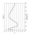
- FIG. 2illustrates exemplary light transmission patterns relative to the thickness of the preferred antimicrobial layer.
- FIG. 3illustrates exemplary transmission spectra from a half-wave Ti0 2 layered optical window for a monochromatic light source.
- FIG. 4Ais a frontal view of an exemplary circular, planar optical output window covered with an antimicrobial layer of the present invention.
- FIG. 4Bis a side view of the exemplary planar optical output window shown in FIG. 4A .
- FIG. 4Cillustrates application of an antimicrobial layer to a convex skin contacting surface.
- FIG. 5illustrates an exemplary dermatologic treatment apparatus including an antimicrobial skin contacting surface.
- Dermatologic and cosmetic light-source treatment devicesinclude a skin contacting surface that is antimicrobial.
- the antimicrobial skin contacting surfacecomprises a layer that enhances the cleanliness of the device and reduces infection and contamination risks, particularly where the device is used to treat multiple individuals.
- the term “antimicrobial”refers to a material capable of destroying, preventing the development of or inhibiting the pathogenic activity of microorganisms, such as bacteria.
- the materialitself may provide such results, or the material may play a role in the achievement of such results.
- the materialmay promote the formation of reactive oxygen species.
- the materialmay be titanium dioxide (TiO 2 ) or zinc oxide (ZnO).
- TiO 2may be deposited as a transparent layer on a substrate. At least a portion of the substrate may be positioned in the optical path of the dermatologic or cosmetic light-based treatment device.
- a transparent TiO 2 layeris applied as a layer across a sapphire substrate of a laser treatment device.
- the TiO 2 layermay be applied to the optical output windows of the laser treatment devices described in U.S. Pat. Nos. 7,452,356; 7,250,045; and 7,118,563.
- the TiO 2 layermay be applied using a method that minimizes the Fresnel reflective losses at the boundaries between the sapphire substrate and the TiO 2 layer; and/or between the TiO 2 layer and the epidermal surface.
- a single layer high-refractive index TiO 2 layermay be provided on a lower-refractive index substrate, resulting in light transmission loss at the skin (e.g., a fluence reduction, a power density reduction).
- TiO 2 layer to the substratemay be accomplished using an activated reactive electron beam (e-beam) evaporation process, although it will be recognized by those skilled in the art having the benefit of this disclosure that any deposition process producing a layer of desired thickness may be used.
- e-beamreactive electron beam
- the TiO 2 compoundis formed on a heated substrate by electron beam evaporation of TiO (Balzers) in an ionized oxygen medium produced by a cold cathode discharge.
- the layermay be applied so that the entire skin contacting surface of the device is covered, thereby ensuring that the entire surface in contact with the skin comprises antimicrobial material.
- FIGS. 4A and 4Billustrate application of an antimicrobial layer to a planar circular substrate to form an antimicrobial skin contacting surface.
- FIG. 4Cillustrates application of an antimicrobial layer to a convex skin contacting surface.
- the reflection and transmission intensity ratiosare described by a set of basic Fresnel equations, as described for example by Simon Ramo, John R. Whinnery, and Theodore van Duzer, Fields and Waves in Communication Electronics , Chapter 6, 2nd Edition, John Wiley & Sons, Inc. (1984).
- the reflection (R) and the transmission (T) ratiosare:
- Z Lis the load field impedance transformed from the output side
- ⁇is the intrinsic impedance of the input medium.
- the intrinsic impedance ⁇ of a given medium with an oblique rayis given by the following equations for the two orthogonal polarization conditions.
- ⁇is the medium material refractive index
- ⁇ iis the ray angle in the medium relative to the interface normal.
- the load impedance Z Lis calculated by transforming the output medium intrinsic impedance ⁇ L from equation (3) and (4) through the intervening layers using the following equations.
- Z L⁇ i ⁇ [ ⁇ L ⁇ cos ⁇ ( ⁇ ) + i ⁇ ⁇ ⁇ i ⁇ sin ⁇ ( ⁇ ) ⁇ i ⁇ cos ⁇ ( ⁇ ) + i ⁇ ⁇ ⁇ L ⁇ sin ⁇ ( ⁇ ) ] ( 5 )
- ⁇ iis the intervening layers' intrinsic impedance as described by the same equation (3) and (4) with difference refractive indices and ray angles
- ⁇is the propagation phase delay through the layer under consideration. It is worth noting that this is a complex number calculation as shown by the imaginary prefactor i in the equation.
- the propagation phase factor ⁇is the phase number for the optical path length through the thin layer.
- ⁇2 ⁇ ⁇ ⁇ ⁇ O ⁇ nd ⁇ ⁇ cos ⁇ ( ⁇ i ) ( 6 )
- dis the thin layer thickness
- ⁇ ois the free space wavelength for the light source
- ⁇is the layer refractive index
- equations (1) through (7)one can calculate the transmission and reflection intensity ratios at any dielectric interface. These equations were used to calculate the total transmission through a transparent dielectric substrate window coated with an antimicrobial layer on the output side (see FIG. 1 ). Due to the multiple internal reflections, the total net transmission ratio (T) through the coated window can be shown as follows.
- TT 1 ⁇ T 2 ⁇ ( 1 1 - R 2 ⁇ R 3 ) ( 8 )
- FIG. 1the schematics of an exemplary ray 10 incident at an oblique angle onto a thick optical window substrate 20 with its output side coated with a layer 30 of TiO 2 are shown.
- FIG. 1demonstrates, among other things, the multiple bounces within the substrate 20 with internal reflection ratios of R 2 at the output interface 40 and R 3 at the input interface 50 .
- T 1 and T 2are the transmission ratios at the input interface 50 and the output interface 40 , respectively.
- a systemfor use with a light source, such as an 800-nm laser input light source.
- the systemincludes a substrate of optically thick sapphire with a refractive index of about 1.76.
- the output side of the sapphire substrateis coated with a single layer TiO 2 thin hard layer, which has a refractive index of about 2.4.
- the net output transmission of the systemwas calculated using equation (8), shown above, for four different combinations composed of two different input ray angular distributions (normal incidence single ray and Lambertian distribution rays), and two different output contact media (air with a refractive index close to 1, and skin with a refractive index close to 1.4).
- the Lambertian distributionwas the cosine angular intensity distribution.
- the total output transmissionwas calculated by integrating equation (8) for each incidence angle with its cosine weighting factor.
- Total coated substrate transmission ratioswere calculated for the four experimental conditions as a function of the wavelength normalized TiO 2 layer thickness on the output side. The results for the four experimental conditions are shown in FIG. 2 .
- the curve labeled Arepresents a single normal incidence ray with the TiO 2 output surface contacting air.
- the curve labeled Brepresents a single normal incidence ray with the TiO 2 output surface contacting skin.
- the curve labeled Crepresents a Lambertian source with the TiO 2 output surface contacting air.
- the curve labeled Drepresents a Lambertian source with the TiO 2 output surface contacting skin. Layer thicknesses used were between about 100 nm to about 200 nm.
- the TiO 2 layer thicknesswas normalized to the source wavelength in the material, which was equal to ⁇ o /n t .
- ⁇ ⁇was the source free space wavelength of 800 nm
- n twas the TiO 2 refractive index of 2.4.
- net transmissionis higher when the TiO 2 output surface with a high index of refraction was in contact with a much lower refractive index material (e.g., skin).
- the Lambertian ray distributioninvolved a transmission decrease due to the inherently lower transmission of the oblique rays. Transmission with air contact was lower as compared to transmission with skin contact. However, all curves exhibited the same general transmission modulation pattern relative to the different layer thicknesses. In each case, net transmission may be optimized at the multiples of half material wavelength. For an 800-nm source, the TiO 2 (refractive index of about 2.4) half-wave layer thickness was about 167 nm. This half-wave layer thickness was also shown to be independent of the source wavelength.
- the refractive loss introduced by the inclusion of the high index layer of TiO 2was minimized, while at the same time ensuring that the skin is contacted only by the TiO 2 and not by the sapphire.
- a TiO 2 thin layerwas deposited by reactive electron-beam evaporation of TiO (Balzers) onto a heated (80° C.) sapphire substrate in an ionized oxygen medium, according to the method described by K. Narashimha Rao and S. Mohan, in “Optical properties of electron-beam evaporated TiO 2 layers deposited in an ionized oxygen medium”, Journal of Vacuum Science & Technology A: Vacuum, Surfaces and Films 8(4), p. 3260-3264 (1990).
- a 5 nm thick SiO adhesion coatingwas applied to the sapphire substrate prior to deposition of the TiO 2 layer.
- the adhesion coatingdid not appear to reduce significantly the transmission as compared to the completed optical system with the sapphire substrate and the TiO 2 layer.
- the output transmission spectrawere measured with a spectrophotometer and the results are shown in FIG. 3 .
- the measured net transmission of 87% at 800-nm wavelengthgenerally agrees well with the calculated value of 85% for normal incidence and air contact, with the variation likely due in large measure to the limitations of the measurement equipment and/or test set-up.
- FIG. 3was also tested using a Lambertian source (SpectraGenies iEpi hair removal device). No output loss was measured despite the high refractive index TiO 2 layer (again, likely due in large measure to the limitations of the measurement equipment and/or test set-up). Accordingly, a device including a high refractive-index antimicrobial optical layer as a skin contact surface may be optimized in part by minimizing the loss associated with the presence of the layer.
- an exemplary substrate with an antimicrobial layercan be better appreciated.
- the substrate 400is shown in front plan view, while in FIG. 4B the substrate 400 is shown in side view.
- the antimicrobial layer 405is shown relative to the substrate 400 , which can be sapphire or other similar material.
- the installation of the substrate with the antimicrobial layer into a treatment devicecan be better appreciated.
- the device 500includes a light source 580 which conveys light into a mixer 540 supported within a barrel 530 .
- An air gap 525may exist between the barrel and the mixer.
- the substrate portion 560Pressed, fixedly placed, or otherwise positioned into the front of the barrel 530 is the substrate portion 560 . Covering the portion 560 is the antimicrobial layer 550 , which forms the only surface of the device 500 that contacts the skin, thus promoting reduced infection and/or contamination that might occur from use of the device. It will be appreciated that, while the substrate shown in the illustrated embodiment of FIG. 5 is flat and lacks surface shape, a shaped layer or surface also may be used, including but not limited to a layer or surface applied to a convex substrate 409 , in which case the antimicrobial layer 407 is also convex (see FIG. 4C ).
- Device optimizationmay depend upon the type of device. For example, a device which emits light continuously (i.e., non-pulsed light) may be optimized by increasing the intensity of the device light source in order to maintain at the skin a desired fluence. A device which emits pulsed light may be optimized by increasing the intensity of the light source, extending the pulse width, or some combination of both steps, to maintain at the skin a desired fluence or power density. Also, to maintain a desired power density at the skin, a reduced device output aperture or beam size may be used. In some cases, such optimization may occur during manufacture of the device as a result of calibration testing. For example, pulse width might be adjusted automatically in order to achieve a desired fluence for a device.
- Devices including an antimicrobial layer as described hereinmay be characterized as less efficient due to a loss introduced by the presence of such a layer, or due to the nature of certain operational parameters when steps have been taken to reduce or minimize such a loss. For example, less efficient devices might dissipate more heat, use more battery power, produce more light, etc., as compared with other, more efficient devices. Accordingly, device optimization may involve the control of one or more of such operational parameters to achieve a desired device configuration or result.
- antimicrobial substancesmay be used alone or in combination with TiO 2 (e.g., zinc oxide (ZnO)).
- the substancesmay be applied or used in a variety of ways, e.g., in layer form, as particles embedded within layers or surfaces, as nano-particles, etc.
- Reactive oxygen speciesmay be formed using the interaction of light (e.g., blue light having a wavelength of approximately 450-460 nm (e.g. 457 nm)) with appropriate substances (e.g., TiO 2 , riboflavin, riboflavin-5 phosphate, etc.).
- the present inventionis suitable for use with any light source (e.g., light emitting diodes (LEDs)), and is not limited to laser light sources.
- LEDslight emitting diodes
- the inventionis useful with a wide variety of skin treatments or other treatment applications (e.g., hair removal, acne treatment, epilation for the removal of unwanted hair, hair-regrowth inhibition, tattoo removal, treatment of birthmarks, skin rejuvenation, wrinkle reduction, and facial resurfacing).
Landscapes
- Health & Medical Sciences (AREA)
- Life Sciences & Earth Sciences (AREA)
- Physics & Mathematics (AREA)
- Engineering & Computer Science (AREA)
- Biomedical Technology (AREA)
- Optics & Photonics (AREA)
- Surgery (AREA)
- Animal Behavior & Ethology (AREA)
- Veterinary Medicine (AREA)
- Nuclear Medicine, Radiotherapy & Molecular Imaging (AREA)
- Public Health (AREA)
- General Health & Medical Sciences (AREA)
- Otolaryngology (AREA)
- Molecular Biology (AREA)
- Medical Informatics (AREA)
- Heart & Thoracic Surgery (AREA)
- Electromagnetism (AREA)
- Biophysics (AREA)
- Pathology (AREA)
- Radiology & Medical Imaging (AREA)
- Cosmetics (AREA)
- Radiation-Therapy Devices (AREA)
Abstract
Description
where ZLis the load field impedance transformed from the output side, and η is the intrinsic impedance of the input medium.
where η is the medium material refractive index, and θiis the ray angle in the medium relative to the interface normal.
where ηiis the intervening layers' intrinsic impedance as described by the same equation (3) and (4) with difference refractive indices and ray angles, and φ is the propagation phase delay through the layer under consideration. It is worth noting that this is a complex number calculation as shown by the imaginary prefactor i in the equation.
where d is the thin layer thickness, λois the free space wavelength for the light source, and η is the layer refractive index.
n1sin(θ1)=n2sin(θ2) (7)
Claims (19)
half-wave layer thickness=½[λ/n],
half-wave layer thickness=½[λ/n],
Priority Applications (2)
| Application Number | Priority Date | Filing Date | Title |
|---|---|---|---|
| US12/772,104US8512322B1 (en) | 2009-05-01 | 2010-04-30 | Antimicrobial layer for optical output window |
| US13/970,532US8728063B2 (en) | 2009-05-01 | 2013-08-19 | Antimicrobial layer for optical output window |
Applications Claiming Priority (2)
| Application Number | Priority Date | Filing Date | Title |
|---|---|---|---|
| US17493609P | 2009-05-01 | 2009-05-01 | |
| US12/772,104US8512322B1 (en) | 2009-05-01 | 2010-04-30 | Antimicrobial layer for optical output window |
Related Child Applications (1)
| Application Number | Title | Priority Date | Filing Date |
|---|---|---|---|
| US13/970,532ContinuationUS8728063B2 (en) | 2009-05-01 | 2013-08-19 | Antimicrobial layer for optical output window |
Publications (1)
| Publication Number | Publication Date |
|---|---|
| US8512322B1true US8512322B1 (en) | 2013-08-20 |
Family
ID=48952110
Family Applications (2)
| Application Number | Title | Priority Date | Filing Date |
|---|---|---|---|
| US12/772,104Active2030-12-28US8512322B1 (en) | 2009-05-01 | 2010-04-30 | Antimicrobial layer for optical output window |
| US13/970,532ActiveUS8728063B2 (en) | 2009-05-01 | 2013-08-19 | Antimicrobial layer for optical output window |
Family Applications After (1)
| Application Number | Title | Priority Date | Filing Date |
|---|---|---|---|
| US13/970,532ActiveUS8728063B2 (en) | 2009-05-01 | 2013-08-19 | Antimicrobial layer for optical output window |
Country Status (1)
| Country | Link |
|---|---|
| US (2) | US8512322B1 (en) |
Cited By (8)
| Publication number | Priority date | Publication date | Assignee | Title |
|---|---|---|---|---|
| GB2501978A (en)* | 2012-03-22 | 2013-11-13 | Palo Alto Res Ct Inc | Infrared transmissive window with titanium dioxide coating |
| US8728063B2 (en) | 2009-05-01 | 2014-05-20 | Tria Beauty, Inc. | Antimicrobial layer for optical output window |
| US8961578B2 (en) | 2012-03-21 | 2015-02-24 | Tria Beauty, Inc. | Dermatological treatment device with one or more vertical cavity surface emitting lasers (VCSEL) |
| US20150351841A1 (en)* | 2014-06-04 | 2015-12-10 | The Curators Of The University Of Missouri | Guided wave ablation and sensing |
| WO2016099508A1 (en)* | 2014-12-18 | 2016-06-23 | GE Lighting Solutions, LLC | An antimicrobial lighting system |
| US9642358B2 (en) | 2013-12-12 | 2017-05-09 | Ge Lighting Solutions Llc | Antimicrobial lighting system |
| US9724440B2 (en) | 2013-11-15 | 2017-08-08 | GE Lighting Solutions, LLC | Environmental cleaning and antimicrobial lighting component and fixture |
| US20200324137A1 (en)* | 2017-12-20 | 2020-10-15 | Public University Corporation Nagoya City University | Ultraviolet irradiation device, attachment and elastic member for use in ultraviolet irradiation device, and ultraviolet irradiation method |
Citations (18)
| Publication number | Priority date | Publication date | Assignee | Title |
|---|---|---|---|---|
| US4232678A (en) | 1977-05-16 | 1980-11-11 | Joseph Skovajsa | Device for the local treatment of a patient, and more particularly applicable in acupuncture and auriculotheraphy |
| US5735844A (en) | 1995-02-01 | 1998-04-07 | The General Hospital Corporation | Hair removal using optical pulses |
| US5885273A (en) | 1995-03-29 | 1999-03-23 | Esc Medical Systems, Ltd. | Method for depilation using pulsed electromagnetic radiation |
| US6096029A (en) | 1997-02-24 | 2000-08-01 | Laser Skin Toner, Inc. | Laser method for subsurface cutaneous treatment |
| US6277111B1 (en) | 1993-12-08 | 2001-08-21 | Icn Photonics Limited | Depilation |
| US6508813B1 (en) | 1996-12-02 | 2003-01-21 | Palomar Medical Technologies, Inc. | System for electromagnetic radiation dermatology and head for use therewith |
| US20040039242A1 (en)* | 2002-04-02 | 2004-02-26 | Seedling Enterprises, Llc | Apparatus and methods using visible light for debilitating and/or killing microorganisms within the body |
| US6888661B1 (en)* | 2002-06-13 | 2005-05-03 | Cheetah Omni, Llc | Square filter function tunable optical devices |
| US7118563B2 (en) | 2003-02-25 | 2006-10-10 | Spectragenics, Inc. | Self-contained, diode-laser-based dermatologic treatment apparatus |
| US7250045B2 (en) | 2003-02-25 | 2007-07-31 | Spectragenics, Inc. | Self-contained, eye-safe hair-regrowth-inhibition apparatus and method |
| US20080039768A1 (en)* | 2006-08-10 | 2008-02-14 | Medtronic, Inc. | Implantable devices with photocatalytic surfaces for treating hydrocephalus |
| US20080125838A1 (en)* | 2006-08-10 | 2008-05-29 | Medtronic, Inc. | Implantable Devices With Photocatalytic Surfaces |
| US7452356B2 (en) | 2003-02-25 | 2008-11-18 | Tria Beauty, Inc. | Eye-safe dermatologic treatment apparatus |
| US20090275933A1 (en)* | 2008-05-02 | 2009-11-05 | Zelickson Brian D | Laser energy devices and methods for soft tissue removal |
| US20100160904A1 (en)* | 2008-11-24 | 2010-06-24 | Gradiant Research, Llc | Photothermal treatment of soft tissues |
| US7824023B2 (en) | 2005-06-13 | 2010-11-02 | Miyakoshi Printing Machinery Co., Ltd. | Ink furnishing unit in an ink jet recorder |
| US20110152978A1 (en)* | 2008-12-04 | 2011-06-23 | Searete Llc, A Limited Liability Corporation Of The State Of Delaware | Systems, devices, and methods including catheters configured to monitor biofilm formation having biofilm spectral information configured as a data structure |
| US20110190749A1 (en)* | 2008-11-24 | 2011-08-04 | Mcmillan Kathleen | Low Profile Apparatus and Method for Phototherapy |
Family Cites Families (1)
| Publication number | Priority date | Publication date | Assignee | Title |
|---|---|---|---|---|
| US8512322B1 (en) | 2009-05-01 | 2013-08-20 | Tria Beauty, Inc. | Antimicrobial layer for optical output window |
- 2010
- 2010-04-30USUS12/772,104patent/US8512322B1/enactiveActive
- 2013
- 2013-08-19USUS13/970,532patent/US8728063B2/enactiveActive
Patent Citations (19)
| Publication number | Priority date | Publication date | Assignee | Title |
|---|---|---|---|---|
| US4232678A (en) | 1977-05-16 | 1980-11-11 | Joseph Skovajsa | Device for the local treatment of a patient, and more particularly applicable in acupuncture and auriculotheraphy |
| US6277111B1 (en) | 1993-12-08 | 2001-08-21 | Icn Photonics Limited | Depilation |
| US5735844A (en) | 1995-02-01 | 1998-04-07 | The General Hospital Corporation | Hair removal using optical pulses |
| US5885273A (en) | 1995-03-29 | 1999-03-23 | Esc Medical Systems, Ltd. | Method for depilation using pulsed electromagnetic radiation |
| US6197020B1 (en) | 1996-08-12 | 2001-03-06 | Sublase, Inc. | Laser apparatus for subsurface cutaneous treatment |
| US6508813B1 (en) | 1996-12-02 | 2003-01-21 | Palomar Medical Technologies, Inc. | System for electromagnetic radiation dermatology and head for use therewith |
| US6096029A (en) | 1997-02-24 | 2000-08-01 | Laser Skin Toner, Inc. | Laser method for subsurface cutaneous treatment |
| US20040039242A1 (en)* | 2002-04-02 | 2004-02-26 | Seedling Enterprises, Llc | Apparatus and methods using visible light for debilitating and/or killing microorganisms within the body |
| US6888661B1 (en)* | 2002-06-13 | 2005-05-03 | Cheetah Omni, Llc | Square filter function tunable optical devices |
| US7118563B2 (en) | 2003-02-25 | 2006-10-10 | Spectragenics, Inc. | Self-contained, diode-laser-based dermatologic treatment apparatus |
| US7250045B2 (en) | 2003-02-25 | 2007-07-31 | Spectragenics, Inc. | Self-contained, eye-safe hair-regrowth-inhibition apparatus and method |
| US7452356B2 (en) | 2003-02-25 | 2008-11-18 | Tria Beauty, Inc. | Eye-safe dermatologic treatment apparatus |
| US7824023B2 (en) | 2005-06-13 | 2010-11-02 | Miyakoshi Printing Machinery Co., Ltd. | Ink furnishing unit in an ink jet recorder |
| US20080039768A1 (en)* | 2006-08-10 | 2008-02-14 | Medtronic, Inc. | Implantable devices with photocatalytic surfaces for treating hydrocephalus |
| US20080125838A1 (en)* | 2006-08-10 | 2008-05-29 | Medtronic, Inc. | Implantable Devices With Photocatalytic Surfaces |
| US20090275933A1 (en)* | 2008-05-02 | 2009-11-05 | Zelickson Brian D | Laser energy devices and methods for soft tissue removal |
| US20100160904A1 (en)* | 2008-11-24 | 2010-06-24 | Gradiant Research, Llc | Photothermal treatment of soft tissues |
| US20110190749A1 (en)* | 2008-11-24 | 2011-08-04 | Mcmillan Kathleen | Low Profile Apparatus and Method for Phototherapy |
| US20110152978A1 (en)* | 2008-12-04 | 2011-06-23 | Searete Llc, A Limited Liability Corporation Of The State Of Delaware | Systems, devices, and methods including catheters configured to monitor biofilm formation having biofilm spectral information configured as a data structure |
Non-Patent Citations (2)
| Title |
|---|
| Rao, et al., "Optical Properties of Electron-beam Evaporated TiO2 Films Deposited in an Ionized Oxygen Medium", Journal of Vacuum Science & Technology A: Vacuum, Surfaces, and Films, vol. 8, No. 4, pp. 3260-3264. |
| Wong, et al., "Visible-Light-Induced Bactericidal Activity of a Nitrogen-Doped Titanium Photocatalyst against Human Pathogens", Applied and Environmental Microbiology, pp. 6111-6116. |
Cited By (10)
| Publication number | Priority date | Publication date | Assignee | Title |
|---|---|---|---|---|
| US8728063B2 (en) | 2009-05-01 | 2014-05-20 | Tria Beauty, Inc. | Antimicrobial layer for optical output window |
| US8961578B2 (en) | 2012-03-21 | 2015-02-24 | Tria Beauty, Inc. | Dermatological treatment device with one or more vertical cavity surface emitting lasers (VCSEL) |
| GB2501978A (en)* | 2012-03-22 | 2013-11-13 | Palo Alto Res Ct Inc | Infrared transmissive window with titanium dioxide coating |
| GB2501978B (en)* | 2012-03-22 | 2016-07-13 | Palo Alto Res Ct Inc | High infrared transmission window with self cleaning hydrophilic surface |
| US9724440B2 (en) | 2013-11-15 | 2017-08-08 | GE Lighting Solutions, LLC | Environmental cleaning and antimicrobial lighting component and fixture |
| US9642358B2 (en) | 2013-12-12 | 2017-05-09 | Ge Lighting Solutions Llc | Antimicrobial lighting system |
| US20150351841A1 (en)* | 2014-06-04 | 2015-12-10 | The Curators Of The University Of Missouri | Guided wave ablation and sensing |
| US10456198B2 (en)* | 2014-06-04 | 2019-10-29 | The Curators Of The University Of Missouri | Guided wave ablation and sensing |
| WO2016099508A1 (en)* | 2014-12-18 | 2016-06-23 | GE Lighting Solutions, LLC | An antimicrobial lighting system |
| US20200324137A1 (en)* | 2017-12-20 | 2020-10-15 | Public University Corporation Nagoya City University | Ultraviolet irradiation device, attachment and elastic member for use in ultraviolet irradiation device, and ultraviolet irradiation method |
Also Published As
| Publication number | Publication date |
|---|---|
| US20130338736A1 (en) | 2013-12-19 |
| US8728063B2 (en) | 2014-05-20 |
Similar Documents
| Publication | Publication Date | Title |
|---|---|---|
| US8728063B2 (en) | Antimicrobial layer for optical output window | |
| CN101500647B (en) | System of plaster and radiation device | |
| EP0955884A1 (en) | Radiation-delivery device | |
| WO2012158570A1 (en) | Phototherapy system | |
| JP2006334438A (en) | Apparatus and method for photocosmetic and photodermatological treatment | |
| US20140074010A1 (en) | Wearable phototherapy device | |
| US5835648A (en) | Surface illuminator for photodynamic therapy | |
| US20080306471A1 (en) | Methods and devices for fractional ablation of tissue | |
| AU2005274811A1 (en) | Treatment of skin with light and a benefit agent to mitigate acne | |
| WO2012106689A1 (en) | Radiation-based dermatological devices and methods | |
| US12121745B2 (en) | Device and method for UV antisepsis | |
| US10959777B2 (en) | Laser shaving | |
| US10456198B2 (en) | Guided wave ablation and sensing | |
| TW200836791A (en) | Hair growth light management device | |
| CN111420292A (en) | A kind of phototherapy apparatus and its making method | |
| Charamisinau et al. | Semiconductor laser insert with uniform illumination for use in photodynamic therapy | |
| US20080039907A1 (en) | Phototherapy Systems and Methods | |
| KR101561448B1 (en) | Optical curer using light guide plate having fine particle layer | |
| CA3168341A1 (en) | Phototherapy devices and methods | |
| EP1274359A1 (en) | Method and apparatus for superficial skin heat treatment | |
| CN101518672A (en) | Irradiation device for photodynamic therapy | |
| CN111317921A (en) | Phototherapeutic instrument and manufacturing method thereof | |
| Pasricha et al. | Solar UVB Radiation for the Synthesis of Vitamin D3 in Four Skin Types–Model Propagation Studies | |
| CN212547985U (en) | Phototherapy instrument | |
| EP2436332A1 (en) | Light-based skin treatment device |
Legal Events
| Date | Code | Title | Description |
|---|---|---|---|
| AS | Assignment | Owner name:TRIA BEAUTY, INC., CALIFORNIA Free format text:ASSIGNMENT OF ASSIGNORS INTEREST;ASSIGNORS:LIU, HARVEY I.;GROVE, ROBERT E.;WECKWERTH, MARK V.;SIGNING DATES FROM 20100618 TO 20100712;REEL/FRAME:024751/0530 | |
| AS | Assignment | Owner name:ATHYRIUM OPPORTUNITIES FUND (A) LP, NEW YORK Free format text:NOTICE OF GRANT OF SECURITY INTEREST;ASSIGNOR:TRIA BEAUTY, INC.;REEL/FRAME:030740/0215 Effective date:20130702 | |
| STCF | Information on status: patent grant | Free format text:PATENTED CASE | |
| FPAY | Fee payment | Year of fee payment:4 | |
| AS | Assignment | Owner name:CHANNEL INVESTMENTS, LLC, FLORIDA Free format text:ASSIGNMENT OF ASSIGNORS INTEREST;ASSIGNOR:TRIA BEAUTY, INC.;REEL/FRAME:042229/0195 Effective date:20170411 | |
| MAFP | Maintenance fee payment | Free format text:PAYMENT OF MAINTENANCE FEE, 8TH YR, SMALL ENTITY (ORIGINAL EVENT CODE: M2552); ENTITY STATUS OF PATENT OWNER: SMALL ENTITY Year of fee payment:8 | |
| FEPP | Fee payment procedure | Free format text:MAINTENANCE FEE REMINDER MAILED (ORIGINAL EVENT CODE: REM.); ENTITY STATUS OF PATENT OWNER: SMALL ENTITY | |
| FEPP | Fee payment procedure | Free format text:11.5 YR SURCHARGE- LATE PMT W/IN 6 MO, SMALL ENTITY (ORIGINAL EVENT CODE: M2556); ENTITY STATUS OF PATENT OWNER: SMALL ENTITY | |
| MAFP | Maintenance fee payment | Free format text:PAYMENT OF MAINTENANCE FEE, 12TH YR, SMALL ENTITY (ORIGINAL EVENT CODE: M2553); ENTITY STATUS OF PATENT OWNER: SMALL ENTITY Year of fee payment:12 | |
| AS | Assignment | Owner name:AESTHETE HOLDING CORPORATION, DELAWARE Free format text:ASSIGNMENT OF ASSIGNORS INTEREST;ASSIGNOR:CHANNEL INVESTMENTS, LLC;REEL/FRAME:072121/0256 Effective date:20250509 |