US8508848B2 - Exit pupil expanders with wide field-of-view - Google Patents
Exit pupil expanders with wide field-of-viewDownload PDFInfo
- Publication number
- US8508848B2 US8508848B2US12/745,793US74579310AUS8508848B2US 8508848 B2US8508848 B2US 8508848B2US 74579310 AUS74579310 AUS 74579310AUS 8508848 B2US8508848 B2US 8508848B2
- Authority
- US
- United States
- Prior art keywords
- coupling diffractive
- substrate
- optical beam
- coupling
- another
- Prior art date
- Legal status (The legal status is an assumption and is not a legal conclusion. Google has not performed a legal analysis and makes no representation as to the accuracy of the status listed.)
- Active, expires
Links
- 210000001747pupilAnatomy0.000titleclaimsabstractdescription66
- 239000000758substrateSubstances0.000claimsabstractdescription275
- 238000000034methodMethods0.000claimsabstractdescription13
- 238000010168coupling processMethods0.000claimsdescription342
- 238000005859coupling reactionMethods0.000claimsdescription342
- 230000003287optical effectEffects0.000claimsdescription310
- 239000000463materialSubstances0.000claimsdescription56
- 230000000737periodic effectEffects0.000claimsdescription52
- 230000008878couplingEffects0.000claimsdescription12
- 230000000644propagated effectEffects0.000claimsdescription9
- 238000012545processingMethods0.000claimsdescription7
- 230000001902propagating effectEffects0.000claimsdescription5
- 238000005286illuminationMethods0.000abstractdescription9
- 230000004424eye movementEffects0.000description2
- 238000012986modificationMethods0.000description2
- 230000004048modificationEffects0.000description2
- 239000000126substanceSubstances0.000description2
- 238000001429visible spectrumMethods0.000description2
- 238000013459approachMethods0.000description1
- 230000005540biological transmissionEffects0.000description1
- 238000004891communicationMethods0.000description1
- 230000000295complement effectEffects0.000description1
- 230000000694effectsEffects0.000description1
- 230000007613environmental effectEffects0.000description1
- 238000003384imaging methodMethods0.000description1
- 239000004973liquid crystal related substanceSubstances0.000description1
- 230000010287polarizationEffects0.000description1
- 229910052710siliconInorganic materials0.000description1
- 239000010703siliconSubstances0.000description1
- 230000003595spectral effectEffects0.000description1
- 238000001228spectrumMethods0.000description1
Images


Classifications
- G—PHYSICS
- G02—OPTICS
- G02B—OPTICAL ELEMENTS, SYSTEMS OR APPARATUS
- G02B27/00—Optical systems or apparatus not provided for by any of the groups G02B1/00 - G02B26/00, G02B30/00
- G02B27/0081—Optical systems or apparatus not provided for by any of the groups G02B1/00 - G02B26/00, G02B30/00 with means for altering, e.g. enlarging, the entrance or exit pupil
- G—PHYSICS
- G02—OPTICS
- G02B—OPTICAL ELEMENTS, SYSTEMS OR APPARATUS
- G02B27/00—Optical systems or apparatus not provided for by any of the groups G02B1/00 - G02B26/00, G02B30/00
- G02B27/42—Diffraction optics, i.e. systems including a diffractive element being designed for providing a diffractive effect
- G02B27/4272—Diffraction optics, i.e. systems including a diffractive element being designed for providing a diffractive effect having plural diffractive elements positioned sequentially along the optical path
- G—PHYSICS
- G02—OPTICS
- G02B—OPTICAL ELEMENTS, SYSTEMS OR APPARATUS
- G02B5/00—Optical elements other than lenses
- G02B5/18—Diffraction gratings
- G02B5/1814—Diffraction gratings structurally combined with one or more further optical elements, e.g. lenses, mirrors, prisms or other diffraction gratings
- G—PHYSICS
- G02—OPTICS
- G02B—OPTICAL ELEMENTS, SYSTEMS OR APPARATUS
- G02B5/00—Optical elements other than lenses
- G02B5/32—Holograms used as optical elements
Definitions
- the present inventionrelates generally to display devices and, more specifically, to providing a wide field-of-view as well as illumination uniformity in exit pupil expanders that use a plurality of diffractive elements for expanding the exit pupil of a display for viewing.
- the Field-of-View (FOV) of diffractive Exit Pupil Expanders (EPEs) used with Near-to-Eye Displays (NEDs)is typically limited by the refractive index of the available EPE substrate materials.
- the horizontal FOV limitcan be expressed as ( ⁇ H is a half angle of the FOV):
- Equation 1is valid for symmetric exit pupil expansion, i.e., the grating period of the in-coupling diffraction grating is selected so that the horizontal acceptance angles for light guiding are equal for both +1 and ⁇ 1 diffraction orders.
- Equation 1shows that the FOV of a planar EPE is limited by the refractive index of the materials and the wavelength band of the incident light.
- EPE substrate material MGC171manufactured by MITSUBISHI GAS CHEMICALS
- n 21.71
- an apparatuscomprises: a first substrate of optical material having a first surface and a second surface which is opposite to the first surface; an in-coupling diffractive element disposed on the first or the second surface of the first substrate; one or more out-coupling diffractive elements disposed on the first or the second surface, wherein the in-coupling diffractive element is configured to diffract optical rays of the input optical beam, which are incident from one half space relative to a plane perpendicular to the first substrate and parallel to periodic lines of the in-coupling diffractive element, so as to provide one diffracted optical beam substantially within the first and second surfaces such that at least a portion of the one diffracted optical beam is coupled only to one of the one or more out-coupling diffractive elements; a second substrate of optical material having a further first surface and a further second surface and being positioned substantially parallel to the first substrate and in juxtaposed spaced relationship hereto, wherein the further second surface is opposite to the further first surface; a further
- the in-coupling diffractive elementmay be further configured to diffract optical rays of the input optical beam, which are incident from another half space relative to the plane, to provide another diffracted optical beam substantially within the first and second surfaces such that at least a portion of the another diffracted optical beam is coupled only to another of the one or two out-coupling diffractive elements
- the further in-coupling diffractive elementmay be configured to diffract optical rays of the portion of the input optical beam, which are incident from the one half space relative to the plane, to provide a further another diffracted optical beam substantially within the further first and further second surfaces such that at least a portion of the further another diffracted optical beam is coupled only to another of the one or two further out-coupling diffractive elements which is opposite to the another of the one or more out-coupling diffractive elements
- the one and another of the one or more out-coupling diffractive elementsmay be configured to couple by diffraction parts of the one and another diffr
- each of the two output optical beams and a corresponding each of the two further output optical beamsmay substantially coincide at a predetermined distance range from the second substrate.
- the one and another of the one or more out-coupling diffractive elementsmay be symmetrical relative to the in-coupling diffractive element and the one and another of the one or more further out-coupling diffractive elements may be symmetrical relative to the further in-coupling diffractive element.
- distances from the one and another of the one or more out-coupling diffractive elements to the in-coupling diffraction elementmay be different than corresponding distances from the one and another of the one or more further out-coupling diffractive elements to the further in-coupling diffractive element.
- optical rays of the output optical beam and of the further output optical beammay be substantially parallel to corresponding optical rays of the input optical beam.
- the in-coupling diffractive elementwhen using identical materials and identical surrounding material for the first and second substrates, may have a period of the periodic lines equal to a maximum wavelength of the input optical beam divided by an index of refraction of the first and second substrates, and the further in-coupling diffractive element may have a further period of the further periodic lines equal to a minimum wavelength of the input optical beam divided by an index of refraction of a surrounding material of the first and second substrates.
- the further in-coupling diffractive elementwhen using identical materials and identical surrounding material for the first and second substrates, may have a further period of the further periodic lines equal to a maximum wavelength of the input optical beam divided by an index of refraction of the first and second substrates, and the in-coupling diffractive element may have a period of the periodic lines equal to a minimum wavelength of the input optical beam divided by an index of refraction of a surrounding material of the first and second substrates.
- a width of the in-coupling diffraction element in a direction perpendicular to the periodic linesmay be different from a corresponding width of the further in-coupling diffractive element in a direction perpendicular to the further periodic lines.
- the two or more out-coupling diffractive elements, the in-coupling diffractive element, the one or more further out-coupling diffractive elements and the further in-coupling diffractive elementmay have parallel periodic lines.
- the apparatusmay further comprise one or more further substrates, positioned substantially parallel to the first and second substrates and in juxtaposed spaced relationship thereto, with in-coupling and out-coupling diffractive elements disposed on respective surfaces of the one or more further substrates, wherein each of the one or more further substrates with the disposed diffractive elements may be substantially identical to the first substrate with the in-coupling diffractive element and the one or more out-coupling diffraction element or to the second substrate with the further in-coupling diffractive element and the one or more further out-coupling diffraction elements.
- the apparatusmay further comprise one or more further substrates, positioned substantially parallel to the first and second substrates and in juxtaposed spaced relationship thereto, with in-coupling and out-coupling diffractive elements disposed on respective surfaces of the one or more further substrates, wherein each of the one or more further substrates with the disposed diffractive elements may be configured to perform a non-symmetric exit pupil extension for larger incidence angles of the input optical beam than the first substrate with the in-coupling diffractive element and the one or more out-coupling diffraction element or the second substrate with the further in-coupling diffractive element and the one or more further out-coupling diffraction elements.
- the apparatusmay further comprise one or more further substrates, positioned substantially parallel to the first and second substrates and in juxtaposed spaced relationship thereto, with in-coupling and out-coupling diffractive elements disposed on respective surfaces of the one or more further substrates, wherein each of the one or more further substrates with the disposed diffractive elements may be configured to perform a symmetric exit pupil extension only for smaller incidence angles of the input optical beam than the first substrate with the in-coupling diffractive element and the one or more out-coupling diffraction element or the second substrate with the further in-coupling diffractive element and the one or more further out-coupling diffraction elements.
- a material surrounding the first and second substratesmay be air.
- the apparatusmay further comprise one or more intermediate diffractive elements disposed on the first substrate and one or more further intermediate diffractive elements disposed on the second substrate such that at least parts of the input optical beam diffracted in the in-coupling diffractive element and in the further in-coupling diffractive element may be first coupled to corresponding the one or more intermediate diffractive elements and the one or more further intermediate diffractive elements, which are configured to further couple by diffraction corresponding optical beams to the one or more out-coupling diffractive elements and to the one or more further out-coupling diffractive elements, for providing one or more output optical beams and one or more further output optical beams with the expanded exit pupil in the two dimensions.
- the input optical beammay be emanated from a virtual image of a display or a microdisplay.
- grooves of the in-coupling diffractive element or the further in-coupling diffractive elementmay have an asymmetric groove shape and may be slanted gratings.
- a methodcomprises: receiving an input optical beam by an in-coupling diffractive element disposed on a first or a second surface of a first substrate, wherein the second surface is opposite to the first surface; diffracting optical rays of the input optical beam, which are incident from one half space relative to a plane perpendicular to the first substrate and parallel to periodic lines of the in-coupling diffractive element, using the in-coupling diffractive element disposed on the first or the second surface, so as to provide one diffracted optical beam substantially within the first and second surfaces such that at least a portion of the one diffracted optical beam is coupled only to one of one or more out-coupling diffractive elements disposed on the first or the further second surface of the first substrate; coupling by diffraction parts of the one diffracted optical beams from the first substrate using the one of the one or more out-coupling diffractive elements for providing an output optical beam out of the first substrate with an expanded exit pupil in one or two dimensions, and propagating
- the methodmay further comprise: diffracting optical rays of the input optical beam, which are incident from another half space relative to the plane, to provide another diffracted optical beam substantially within the first and second surfaces such that at least a portion of the another diffracted optical beam is coupled only to another of the one or two out-coupling diffractive elements, wherein the another of the one or more out-coupling diffractive elements disposed on the first or the second surface of the first substrate; coupling by diffraction parts of the another diffracted optical beam from the first substrate using another of the one or more out-coupling diffractive elements for providing another output optical beam out of the first substrate with an expanded exit pupil in one or two dimensions, and propagating the another output optical beam through the second substrate; diffracting optical rays of the portion of the input optical beam, which are incident from the one half space relative to the plane, using the further in-coupling diffractive element to provide a further another diffracted optical beam substantially within the further first and further second surfaces such that at least
- the one and another of the one or more out-coupling diffractive elementsmay be symmetrical relative to the in-coupling diffractive element and the one and another of the one or more further out-coupling diffractive elements may be symmetrical relative to the further in-coupling diffractive element.
- distances from the one and another of the one or more out-coupling diffractive elements to the in-coupling diffraction elementmay be different than corresponding distances from the one and another of the one or more further out-coupling diffractive elements to the further in-coupling diffractive element.
- the in-coupling diffractive elementwhen using identical materials and identical surrounding material for the first and second substrates, may have a period of the periodic lines equal to a maximum wavelength of the input optical beam divided by an index of refraction of the first and second substrates, and the further in-coupling diffractive element may have a further period of the further periodic lines equal to a minimum wavelength of the input optical beam divided by an index of refraction of a surrounding material of the first and second substrates or, when using identical materials and identical surrounding material for the first and second substrates, the further in-coupling diffractive element may have a further period of the further periodic lines equal to a maximum wavelength of the input optical beam divided by an index of refraction of the first and second substrates, and the in-coupling diffractive element may have a period of the periodic lines equal to a minimum wavelength of the input optical beam divided by an index of refraction of a surrounding material of the first and second substrates.
- the two or more out-coupling diffractive elements, the in-coupling diffractive element, the one or more further out-coupling diffractive elements and the further in-coupling diffractive elementmay have parallel periodic lines.
- an electronic devicecomprises:
- the in-coupling diffractive elementmay be further configured to diffract optical rays of the input optical beam, which are incident from another half space relative to the plane, to provide another diffracted optical beam substantially within the first and second surfaces such that at least a portion of the another diffracted optical beam is coupled only to another of the one or two out-coupling diffractive elements
- the further in-coupling diffractive elementmay be configured to diffract optical rays of the portion of the input optical beam, which are incident from the one half space relative to the plane, to provide a further another diffracted optical beam substantially within the further first and further second surfaces such that at least a portion of the further another diffracted optical beam is coupled only to another of the one or two further out-coupling diffractive elements which is opposite to the another of the one or more out-coupling diffractive elements
- the one and another of the one or more out-coupling diffractive elementsmay be configured to couple by diffraction parts of the one and another diffr
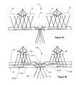
- FIGS. 1 a and 1 bare schematic representations of a symmetric exit pupil expander in a Near-to-Eye Display (NED): a general 3-dimensional view is shown in FIG. 1 a , and a cross sectional view demonstrating propagation of optical rays of the input optical beams from left and right half space is shown in FIG. 1 b;
- NEDNear-to-Eye Display
- FIG. 2is a cross-sectional view of a non-symmetric exit pupil expander demonstrating propagation of optical rays of the input optical beams from left and from right half space, according to an embodiment of the present invention
- FIG. 3is a schematic representation (cross-sectional view) demonstrating a geometry of in-coupling diffractive elements (diffraction gratings) implemented as slanted asymmetric gratings, according to an embodiment of the present invention
- FIGS. 4 a - 4 dare graphs of simulated efficiencies of in-coupling diffraction gratings of FIG. 3 with 50 degrees slanted angle in corresponding left and right regions as a function of a incidence angle, according to an embodiment of the present invention
- FIGS. 5 a and 5 bare schematic representations (cross sectional views) demonstrating improving of out-coupling efficiency of a non-symmetric exit-pupil expander designed according to an embodiment of the present invention as shown in FIG. 5 b compared to out-coupling efficiency of a symmetric exit-pupil expander shown in FIG. 5 a,
- FIG. 6is a schematic representation (cross sectional views) demonstrating improving of in-coupling efficiency of a non-symmetric exit-pupil expander having multiple stacked substrates, according to an embodiment of the present invention
- FIGS. 7 a and 7 bare schematic representations (top views) of one area (left or right) of a two-dimensional diffractive exit pupil expander, wherein an intermediate diffractive element (grating) has an odd number of first order diffractions (shown in FIG. 7 a ) or an even number of further first order reflections (shown in FIG. 7 b ), according to embodiments of the present invention;
- FIG. 8is a flow chart demonstrating propagation of optical rays of the input optical beams from left and right half spaces of a non-symmetric exit pupil expander, according to an embodiment of the present invention.
- FIG. 9is a schematic representation of an electronic device, having an exit pupil expander system, according to embodiments of the present invention.
- a new method and apparatusare presented for providing a wide field-of-view as well as for improving illumination uniformity in Exit Pupil Expanders (EPE) using stacked EPE substrates (or plates) with non-symmetric exit pupil expansion that use a plurality of diffractive elements for expanding the exit pupil of a display for viewing.
- EPEExit Pupil Expanders
- the embodiments of the present inventioncan be applied to a broad optical spectral range of optical beams but most importantly to a visible part of the optical spectrum where the optical beams are called light beams.
- the term “substrate”can be interpreted as a thin plate with two flat or non-flat surfaces (e.g., first and second surfaces) parallel and opposite to each other. All examples for different embodiments of the present invention provided herein are for flat substrates but in principle these embodiments can be applied to non-flat stacked EPE substrates as well.
- embodiments of the present inventionenable to increase field of view without the need for high refractive index materials.
- the embodiments of the present inventionenable reduction of the refractive index requirement to reach a given FOV as compared with traditional symmetric EPE plate. This would allow utilization of readily available materials with lower price and improved optical/environmental characteristics as compared with more exotic substrate materials such as MGC171 (manufactured by MITSUBISHI GAS CHEMICALS) with the refractive index of 1.71.
- improvement of the illumination uniformity of the virtual displaycan be also achieved using embodiments of the present invention.
- an optical devicee.g., the optical device can be a part of a virtual reality display
- an exit pupil expandercan comprise two (or more) substrates of optical material.
- a non-symmetric EPEcomprising two substrates, wherein a first substrate has a first surface and a second surface (opposite to the first surface) and a second substrate has a further first surface and a further second surface (opposite to the further first surface) and being positioned substantially parallel to the first substrate and in juxtaposed spaced relationship hereto.
- the input optical beam emanated from an object or a virtual objectcan be received by an in-coupling diffractive element disposed on the first or the second surface of the first substrate.
- optical rays of the input optical beamwhich are incident from one half space relative to a plane perpendicular to the first substrate and parallel to periodic lines of the in-coupling diffractive element (e.g., diffraction grating), can be diffracted by the in-coupling diffractive element to provide one diffracted optical beam substantially within the first and second surfaces of the first substrate such that at least a portion of the one diffracted optical beam is coupled (e.g., using total internal reflection in the first substrate and optionally using an intermediate diffraction grating for two-dimensional expansion) only to one of one or more out-coupling diffractive elements (e.g., one out-coupling diffractive element for a monocular viewing, two out-coupling diffractive element for a binocular viewing, etc.) disposed on the first or the second surface; and optical rays of the input optical beam, which are incident from another half space relative to said plane, can be further diffracted to provide another diffracted optical beam substantially within the first and second diffr
- parts of said one and another diffracted optical beamscan be coupled by diffraction from the first substrate using the one or more out-coupling diffractive elements for providing two output optical beams out of the first substrate with an expanded exit pupil in one or two dimensions (two-dimension expansion is provided by using intermediate diffraction gratings), and propagating said output optical beams through the second substrate to viewer eyes.
- a portion of the original input optical beam from the object or the virtual object(e.g., the virtual image of the display or the microdisplay), which propagates through said first substrate (e.g., without changing a direction) into the second substrate, can be received by a further in-coupling diffractive element disposed on the further first or further second surface of the second substrate and substantially in alignment with the in-coupling diffractive element of the first substrate and having further periodic lines parallel to the periodic lines of the in-coupling diffractive element.
- optical rays of the portion of the input optical beam, which are incident from the one half space relative to said planecan be diffracted by the further in-coupling diffractive element to provide a further one diffracted optical beam substantially within said further first and further second surfaces such that at least a portion of said further one diffracted optical beam is coupled (e.g., using the total internal reflection in the second substrate and optionally a further intermediate diffraction grating) only to one of one or more further out-coupling diffractive elements (e.g., one further out-coupling diffractive element for a monocular viewing, two further out-coupling diffractive element for a binocular viewing, etc.) which is opposite to said another of the one or more out-coupling diffractive elements of the first substrate, and optical rays of the portion of the input optical beam, which are incident from the another half space relative to said plane, can be diffracted using the further in-coupling diffractive element to provide a further another diffracted optical beam substantially within the further first
- parts of said further one and further another diffracted optical beams from the second substratecan be coupled using the one or more further out-coupling diffractive elements for providing two further output optical beams out of the second substrate with the expanded exit pupil in the one or two dimensions (two-dimension expansion is provided by using intermediate diffraction gratings) directly to the viewer eyes.
- each of the two output optical beams and a corresponding each of the two further output optical beamscan substantially coincide at a predetermined distance range from the second substrate, thus providing an image to both viewer eyes with a wide field-of-view compared to a one-substrate case (see discussion in regard to FIGS. 1 and 2 ).
- optical rays of the output optical beams and of the further output optical beamsare substantially parallel to corresponding optical rays of the input optical beam.
- the virtual displaycan be monocular or binocular, therefore the scenario described herein can be used for both monocular and binocular viewing.
- the EPE with stacked substratescan be designed only for monocular viewing with one out-coupling grating element in each substrate, wherein these out-coupling grating elements can be substantially opposite to each other and located in the same half sphere relative to a plane perpendicular to the substrates and parallel to periodic lines of the in-coupling diffractive elements.
- the in-coupling diffractive element of the first substratecan have a period of the periodic lines equal to a maximum wavelength (or alternatively equal to a minimum wavelength) of the input optical beam divided by an index of refraction of the first and second substrates (alternatively by an index of refraction of a surrounding material of the first and second substrates), and the further in-coupling diffractive element of the second substrate can have a further period of the further periodic lines equal to a minimum wavelength (alternatively equal to a minimum wavelength) of the input optical beam divided by an index of refraction of a surrounding material of the first and second substrates (or alternatively by an index of refraction of the first and second substrates).
- the surrounding material of the first or the second substratecan be air with index of refraction of 1.
- the two out-coupling diffractive elementscan be symmetrical relative to the in-coupling diffractive element in each substrate.
- the out-coupling diffractive elements and the in-coupling diffractive elements in each substratecan have parallel periodic lines.
- distances from the one or more out-coupling diffractive elements to the in-coupling diffraction element in the first substratemay be the same as or different from (see discussions in reference to FIGS. 5 a and 5 b ) the distances from the corresponding one or more further out-coupling diffractive elements to the further in-coupling diffractive element in the second substrate in order to provide better efficiency and uniformity.
- a width of the in-coupling diffraction element of the first substrate in a direction perpendicular to the periodic linesmay be different from a corresponding width of the further in-coupling diffractive element of the second substrate in a direction perpendicular to the further periodic lines to provide better coupling efficiency (see discussions in reference to FIG. 5 c ).
- the two-dimensional expansioncan be provided by using one or more intermediate diffractive elements disposed on the first substrate and one or more further intermediate diffractive elements disposed on the second substrate such that at least parts of the input optical beam diffracted in the in-coupling diffractive element and in the further in-coupling diffractive element are first coupled to corresponding the one or more intermediate diffractive elements and the one or more further intermediate diffractive elements, which can be configured to further couple by diffraction corresponding optical beams to the one or more out-coupling diffractive elements and to the one or more further out-coupling diffractive elements, respectively, for providing the one or more output optical beams and one or more further output optical beams with the expanded exit pupil in two dimensions (see further discussions in reference to FIGS.
- the intermediate diffractive elementcan have an odd number of first order diffractions or an even number of further first order reflections as known in the art and, e.g., described by T. Levola in “Diffractive Optics for Virtual Reality Displays”, SID Eurodisplay 05, Edinburg (2005), SID 02 Digest, Paper 22.1.
- the in-coupling diffractive elementscan be implemented using a variety of different types of diffraction gratings, e.g., planar diffraction gratings manufactured using lithographic methods or classically ruled (having different groove angles and profiles, such as binary, triangular, sinusoidal, etc.).
- the diffractive elementsi.e., their grooves
- the slanted gratingscan be asymmetric such that their slanting angles are equal but have opposite signs relative to the optical axis of the input optical beam, i.e., the groove shapes are mirror images of each other.
- grooves of the in-coupling diffractive element or the further in-coupling diffractive elementcan have an asymmetric groove shape and implemented, e.g., as slanted diffraction gratings (see further discussions in reference to FIGS. 3 and 4 ).
- the EPE devicecan further comprise one or more further substrates, positioned substantially parallel to the first and second substrates, described herein, and in juxtaposed spaced relationship thereto, with in-coupling and out-coupling diffraction elements disposed on respective surfaces of the one or more further substrates, wherein each of the one or more further substrates with the disposed diffractive elements is substantially identical to the first substrate with the in-coupling diffractive element and the one or more out-coupling diffraction elements or to the second substrate with the further in-coupling diffractive element and the one or more further out-coupling diffraction elements.
- non-flat substratescan be cylindrical (e.g., see PCT patent application, International Publication Number WO2006064301), spherical or aspheric as described in co-pending PCT application filed on the same date, International Publication Number WO2009077803 (PCT/IB2007/003965).
- the term “aspheric”can be broadly defined as a surface with a profile that is neither a portion of a sphere nor of a circular cylinder and it is not flat and can be described by complex equations, wherein simple examples can include but are not limited to parabola, hyperbola, ellipse, etc.
- FIGS. 1 a and 1 bshows an example of a schematic representations of a symmetric exit pupil expander (EPE) 1 in a Near-to-Eye Display (NED) application: a general 3-dimentional view is shown in FIG. 1 a , and a cross sectional view demonstrating propagation of optical rays of the input optical beams from left and right half space is shown in FIG. 1 b .
- Input optical rays 5 and 6 emanated from a virtual image of a display (e.g., a microdisplay) 7are coupled into a planar light guide plate (substrate) 4 using a diffraction grating 2 .
- a displaye.g., a microdisplay
- the in-coupled rayspropagate inside the light guide plate by a way of total internal reflection (TIR).
- TIRtotal internal reflection
- Pupil expansion for the input imageis achieved using a second diffraction gratings 3 - 1 and 3 - 2 that couple out parts of the coupled (trapped) light as output beams 5 - 6 and 6 - 5 to provide an image of the microdisplay 7 .
- the whole Field-of-View (FOV) spanned by the input optical rays( ⁇ h is an incidence angle) must be coupled into the light guide plate by the in-coupling grating.
- the whole FOVmust be provided for both eyes, i.e., to left and right branches of the EPE 1 .
- the input optical rays 6 incident from the right half spacemust be coupled to both the left and right eyes of the viewer, and the same must hold for the input optical rays 5 incident from the left half space.
- Proper light in-couplingis achieved when the following two conditions are met.
- the incidence angle of the in-coupled light with respect to a plane normal of the light guide platemust be large enough to support TIR.
- the incidence anglecan be increased by reducing the grating period of the in-coupling grating.
- FIG. 2shows one example among others of a cross-sectional view of a non-symmetric exit pupil expander 10 for demonstrating propagation of optical rays 16 and 18 of the input optical beams from the left and right half spaces, according to an embodiment of the present invention.
- the operation of the non-symmetric EPEcan be understood by considering the light in-coupling for rays that propagate along xz-plane, i.e., horizontal rays.
- the grating period for in-coupling and out-coupling areas of the first EPE platecan be selected so that light from the right half space ( ⁇ i is an incidence angle) is coupled to the left eye of the viewer and the light from the left half space is coupled to the right eye.
- the grating periods of the second EPE platecan be selected so that couplings are reversed.
- optical rays 18 incident from the right half spacecan be coupled only to the right branch of the first EPE substrate 12 .
- optical rays 16 incident from the left half spacecan be coupled only to the left branch of the first EPE plate 12 .
- polychromatic illuminationthis can be achieved if the grating period of the in-coupling grating 12 - 1 of the first EPE substrate 12 is selected as
- d 1⁇ max n 2 , ( 2 ) wherein ⁇ max is a maximum wavelength of the polychromatic incident light and n 2 is the refractive index of the EPE substrates 12 and 14 (assuming that these substrates are made from the same material).
- optical rays 18 incident from the right half spacecan be coupled only to the left branch of the second EPE substrate 14 .
- optical rays 16 incident from the left half spacecan be coupled only to the right branch of the EPE substrate 14 .
- the grating period of the in-coupling diffraction grating 14 - 1 of the second EPE substrate 14is selected as
- d 2⁇ min n 1 , ( 3 ) wherein ⁇ min is a minimum wavelength of the polychromatic incident light and n 1 is the refractive index of surrounding material (e.g., equal to 1 for air) of the EPE substrates 12 and 14 (assuming that these substrates have the same surrounding material).
- ⁇ minis a minimum wavelength of the polychromatic incident light
- n 1is the refractive index of surrounding material (e.g., equal to 1 for air) of the EPE substrates 12 and 14 (assuming that these substrates have the same surrounding material).
- the viewercan see an output optical beams 20 and 22 coupled by corresponding out-coupling diffraction gratings 12 - 2 a and 12 - 2 b from the first EPE substrate 12 and coupled by corresponding out-coupling diffraction gratings 14 - 2 a and 14 - 2 b from the second EPE substrate 14 .
- the FOV of the input optical beam that can be observed through the EPE 10can be determined by considering the combined criteria for the existence of the diffraction orders as explained above and existence of the TIR inside the plates. This results for the horizontal FOV of the stacked non-symmetric EPE discussed herein can be expresses as follows:
- Equation 4shows that the non-symmetric EPE enables FOV improvement with respect to the symmetric case (see Equation 1 and FIGS. 1 a and 1 b ) by a factor of
- EPE substrates 12 and 14can be reversed according to another embodiment of the present invention, as stated herein.
- a further improvement of the FOVmay be obtained by using additional one or more EPE plates or one or more EPE plate pairs designed to operate at larger complementary incidence angles outside of the angular acceptance range of the original non-symmetric EPE plates or EPE plate pairs.
- the EPE stackneed not be an even combination of the EPE plates: for example it could an even or odd number of plates including, e.g., one or more symmetric EPE plates and two or more non-symmetric EPE plates (e.g., on or more EPE pairs) operating at incidence angles outside (i.e., larger than) the angular acceptance range of the one or more symmetric EPE plates.
- FIG. 3shows one example among others of a schematic representation (cross-sectional view) demonstrating a geometry of in-coupling diffractive elements (diffraction gratings) 12 - 1 and 14 - 1 implemented as asymmetric slanted asymmetric gratings with 50 degrees slanting angle, according to an embodiment of the present invention.
- the grating, optical rays and substrate numberscorrespond to the reference numbers of corresponding components shown in FIG. 2 .
- Grooves of the in-coupling diffractive elements 12 - 1 and 14 - 1have grooves with an asymmetric groove shape: 12 - 1 a and 14 - 1 a on the left in region 1 and 12 - 1 b and 14 - 1 b on the right in region II, respectively.
- FIGS. 4 a - 4 dshows an example among others of graphs of simulated (using Rigorous Fourier Modal Method for multilayer surface relief gratings) efficiencies ⁇ of the in-coupling slanted diffraction gratings 12 - 1 and 14 - 1 shown in FIG. 3 with 50 degrees slanted angle in corresponding left and right regions (indicated in FIG. 3 ) as a function of the incidence angle ⁇ as defined herein, according to embodiments of the present invention.
- ⁇is the angle between the x axis (shown in FIGS.
- FIGS. 5 a and 5 bshow examples among others of schematic representations (cross sectional views) demonstrating improving of out-coupling efficiency of a non-symmetric exit-pupil expander designed according to an embodiment of the present invention as shown in FIG. 5 b compared to out-coupling efficiency of a symmetric exit-pupil expander shown in FIG. 5 a .
- the grating, optical rays and substrate numberscorrespond to the reference numbers of corresponding components shown in FIGS. 1 a , 1 b and 2 , respectively.
- out-coupling gratings(exit pupil size) must span the whole FOV and thus cover the whole eye movement range, wherein areas 8 represent “wasted” light.
- size of out-coupling gratings for each plateneeds to span only half FOV and, thus, only half of the eye movement range. This allows for optimum positioning of the out-coupling areas to reduce the amount of “wasted” light.
- the non-symmetric expandercan be utilized to improve the illumination uniformity of the EPE. As shown in FIG.
- the positioning of the out-coupling gratings 12 - 2 a , 12 - 2 b , 14 - 2 a and 14 - 2 bcan be optimized separately for each half space with respect to left/right eye position. This enables improvement in the left/right eye illumination symmetry, illumination uniformity and reduction of unwanted light losses as described herein.
- FIG. 6shows an example among others of a schematic representation (cross sectional views) demonstrating improving of in-coupling efficiency of a non-symmetric exit-pupil expander having multiple stacked substrates (only in-coupling region is shown), according to an embodiment of the present invention.
- the grating, optical rays and substrate numberscorrespond to the reference numbers of corresponding components shown in FIG. 2 .
- FIG. 6shows the case when one or more additional EPE substrates are added compared to the 2-substrate arrangement shown in FIGS. 2 and 3 (only substrate 30 with an in-coupling grating 30 - 1 is shown) to accommodate a broad wavelength band.
- FIG. 6demonstrate that an improvement in coupling efficiency can be achieved by increasing the width of the in-coupling gratings 14 - 1 and 30 - 1 such that more light can be collected at the ends of the gratings 14 - 1 and 30 - 1 .
- FIGS. 7 a and 7 bshow examples among others of schematic representations (top views) of one area (left or right) of a two-dimensional diffractive exit pupil expander according to embodiments of the present invention, wherein an intermediate diffractive element (grating) 24 or 26 has an odd number of first order diffractions (shown in FIG. 7 a ) or an even number of further first order reflections (shown in FIG. 7 b ), as described by T. Levola in “Diffractive Optics for Virtual Reality Displays”, SID Eurodisplay 05, Edinburg (2005), SID 02 Digest, Paper 22.1.
- the angle ⁇is a rotation angle between the periodic lines of the intermediate diffraction grating 26 and the in-coupling grating 12 - 1 or 14 - 1 . respectively.
- the grating and substrate numbers in FIGS. 7 a and 7 bcorrespond to the reference numbers of corresponding components shown in FIG. 2 .
- FIG. 8shows a flow chart demonstrating propagation of optical rays of the input optical beams from left and right half space of a non-symmetric exit pupil expander, according to an embodiment of the present invention.
- a first step 40an input optical beam is received by in-coupling diffraction gratings of the first and second substrates.
- a next step 42optical rays coming from different half spaces are diffracted by the in-coupling grating of the first substrate to only one corresponding out-coupling grating (by TIR in the first substrate and optionally using an intermediate grating in the first substrate for two-dimensional expansion).
- the provided optical componentsare coupled out by the out-coupling diffraction gratings from the first substrate (the out-coupled optical components are propagated through the second substrate to the viewer eyes) thus providing two output optical beams out of the second substrate with the expanded exit pupil in the one or two dimensions.
- a next step 46optical rays coming from different half spaces are diffracted by the in-coupling grating of the second substrate to only one corresponding out-coupling grating (by TIR in the second substrate and optionally using an intermediate grating in the second substrate for two-dimensional expansion) which is opposite to corresponding out-coupling gratings of the first substrate.
- the provided optical componentsare coupled out by the out-coupling gratings from the second substrate to the viewer eyes, providing two further output optical beams out of the second substrate with the expanded exit pupil in the one or two dimensions.
- FIG. 9is a schematic representation of an electronic device, having an exit pupil expander system, according to embodiments of the present invention.
- FIG. 9shows an example of a schematic representation of an electronic device 100 , having the exit pupil expander (EPE) system 10 ( 10 a , or 10 b ) according to an embodiment of the present invention.
- EPEexit pupil expander
- the exit pupil expander (EPE) 10 , 10 a or 10 bcan be used in an electronic (portable) device 100 , such as a mobile phone, personal digital assistant (PDA), communicator, portable Internet appliance, hand-hand computer, digital video and still camera, wearable computer, computer game device, specialized bring-to-the-eye product for viewing and other portable electronic devices.
- the portable device 100has a housing 210 to house a communication unit 212 for receiving and transmitting information from and to an external device (not shown).
- the portable device 100also has a controlling and processing unit 214 for handling the received and transmitted information, and a virtual display system 230 for viewing.
- the virtual display system 230includes a micro-display or an image source 192 and an optical engine 190 .
- the controlling and processing unit 214is operatively connected to the optical engine 190 to provide image data to the image source 192 to display an image thereon.
- the EPE 10can be optically linked to an optical engine 190 .
- the image source 192can be a sequential color LCOS (Liquid Crystal On Silicon) device, an OLED (Organic Light Emitting Diode) array, an MEMS (MicroElectro Mechanical System) device or any other suitable micro-display device operating in transmission, reflection or emission.
- LCOSLiquid Crystal On Silicon
- OLEDOrganic Light Emitting Diode
- MEMSMicroElectro Mechanical System
- the electronic device 100can be a portable device, such as a mobile phone, personal digital assistant (PDA), communicator, portable Internet appliance, hand-held computer, digital video and still camera, wearable computer, computer game device, specialized bring-to-the-eye product for viewing and other portable electronic devices.
- PDApersonal digital assistant
- the exit pupil expandercan also be used in a non-portable device, such as a gaming device, vending machine, band-o-matic, and home appliances, such as an oven, microwave oven and other appliances and other non-portable devices.
Landscapes
- Physics & Mathematics (AREA)
- General Physics & Mathematics (AREA)
- Optics & Photonics (AREA)
- Diffracting Gratings Or Hologram Optical Elements (AREA)
Abstract
Description
- a data processing unit;
- an optical engine operatively connected to the data processing unit for receiving image data from the data processing unit;
- a display device operatively connected to the optical engine for forming an image based on the image data; and
- an exit pupil expander comprising: a first substrate of optical material having a first surface and a second surface which is opposite to the first surface; an in-coupling diffractive element disposed on the first or the second surface of the first substrate; one or more out-coupling diffractive elements disposed on the first or the second surface, wherein the in-coupling diffractive element is configured to diffract optical rays of the input optical beam, which are incident from one half space relative to a plane perpendicular to the first substrate and parallel to periodic lines of the in-coupling diffractive element, so as to provide one diffracted optical beam substantially within the first and second surfaces such that at least a portion of the one diffracted optical beam is coupled only to one of the one or more out-coupling diffractive elements; a second substrate of optical material having a further first surface and a further second surface and being positioned substantially parallel to the first substrate and in juxtaposed spaced relationship hereto, wherein the further second surface is opposite to the further first surface; a further in-coupling diffractive element disposed on the further first or the further second surface substantially in alignment with the in-coupling diffractive element and having further periodic lines parallel to the periodic lines of the in-coupling diffractive element, and configured to receive a portion of the input optical beam which propagates through the first substrate into the further substrate; and one or more further out-coupling diffractive elements disposed on the further first or the further second surface and each being substantially opposite to a corresponding diffractive element of the one or more out-coupling diffractive elements, wherein the further in-coupling diffractive element is configured to diffract optical rays of the portion of the input optical beam, which are incident from another half space relative to the plane, to provide a further one diffracted optical beam substantially within the further first and further second surfaces such that at least a portion of the further diffracted optical beam is coupled only to one of the one or more further out-coupling diffractive elements which is opposite to the one of the one or more out-coupling diffractive elements, and wherein the one of the one or more out-coupling diffractive elements is configured to couple by diffraction parts of the one diffracted optical beam from the first substrate for providing an output optical beam out of the first substrate with an expanded exit pupil in one or two dimensions, the output optical beam being propagated through the second substrate, and the one of the one or more further out-coupling diffractive elements is configured to couple by diffraction parts of the further one diffracted optical beams from the second substrate for providing a further output optical beam out of the second substrate with the expanded exit pupil in the one or two dimensions.
wherein λmaxis a maximum wavelength of the polychromatic incident light and n2is the refractive index of the
wherein λminis a minimum wavelength of the polychromatic incident light and n1is the refractive index of surrounding material (e.g., equal to 1 for air) of the
Claims (25)
Applications Claiming Priority (1)
| Application Number | Priority Date | Filing Date | Title |
|---|---|---|---|
| PCT/IB2007/003960WO2009077802A1 (en) | 2007-12-18 | 2007-12-18 | Exit pupil expanders with wide field-of-view |
Publications (2)
| Publication Number | Publication Date |
|---|---|
| US20100296163A1 US20100296163A1 (en) | 2010-11-25 |
| US8508848B2true US8508848B2 (en) | 2013-08-13 |
Family
ID=39469561
Family Applications (1)
| Application Number | Title | Priority Date | Filing Date |
|---|---|---|---|
| US12/745,793Active2029-01-18US8508848B2 (en) | 2007-12-18 | 2007-12-18 | Exit pupil expanders with wide field-of-view |
Country Status (3)
| Country | Link |
|---|---|
| US (1) | US8508848B2 (en) |
| EP (1) | EP2225592B1 (en) |
| WO (1) | WO2009077802A1 (en) |
Cited By (114)
| Publication number | Priority date | Publication date | Assignee | Title |
|---|---|---|---|---|
| US20130063815A1 (en)* | 2011-09-08 | 2013-03-14 | Seiko Epson Corporation | Electronic apparatus |
| US20140140653A1 (en)* | 2012-11-16 | 2014-05-22 | Rockwell Collins, Inc. | Transparent waveguide display |
| US20150138248A1 (en)* | 2012-05-03 | 2015-05-21 | Martin Schrader | Image Providing Apparatus, Method and Computer Program |
| US9244280B1 (en) | 2014-03-25 | 2016-01-26 | Rockwell Collins, Inc. | Near eye display system and method for display enhancement or redundancy |
| US9244281B1 (en) | 2013-09-26 | 2016-01-26 | Rockwell Collins, Inc. | Display system and method using a detached combiner |
| US9274339B1 (en) | 2010-02-04 | 2016-03-01 | Rockwell Collins, Inc. | Worn display system and method without requiring real time tracking for boresight precision |
| WO2016054092A1 (en)* | 2014-09-29 | 2016-04-07 | Magic Leap, Inc. | Architectures and methods for outputting different wavelength light out of waveguides |
| US9341846B2 (en) | 2012-04-25 | 2016-05-17 | Rockwell Collins Inc. | Holographic wide angle display |
| US9366864B1 (en) | 2011-09-30 | 2016-06-14 | Rockwell Collins, Inc. | System for and method of displaying information without need for a combiner alignment detector |
| US9507150B1 (en) | 2011-09-30 | 2016-11-29 | Rockwell Collins, Inc. | Head up display (HUD) using a bent waveguide assembly |
| US9519089B1 (en) | 2014-01-30 | 2016-12-13 | Rockwell Collins, Inc. | High performance volume phase gratings |
| US9523852B1 (en) | 2012-03-28 | 2016-12-20 | Rockwell Collins, Inc. | Micro collimator system and method for a head up display (HUD) |
| US20170102544A1 (en)* | 2015-10-08 | 2017-04-13 | Tuomas Vallius | Reducing stray light transmission in near eye display using resonant grating filter |
| US9674413B1 (en) | 2013-04-17 | 2017-06-06 | Rockwell Collins, Inc. | Vision system and method having improved performance and solar mitigation |
| US9715067B1 (en) | 2011-09-30 | 2017-07-25 | Rockwell Collins, Inc. | Ultra-compact HUD utilizing waveguide pupil expander with surface relief gratings in high refractive index materials |
| US9715110B1 (en) | 2014-09-25 | 2017-07-25 | Rockwell Collins, Inc. | Automotive head up display (HUD) |
| US9791703B1 (en) | 2016-04-13 | 2017-10-17 | Microsoft Technology Licensing, Llc | Waveguides with extended field of view |
| US9864208B2 (en) | 2015-07-30 | 2018-01-09 | Microsoft Technology Licensing, Llc | Diffractive optical elements with varying direction for depth modulation |
| US9910276B2 (en) | 2015-06-30 | 2018-03-06 | Microsoft Technology Licensing, Llc | Diffractive optical elements with graded edges |
| US9933684B2 (en) | 2012-11-16 | 2018-04-03 | Rockwell Collins, Inc. | Transparent waveguide display providing upper and lower fields of view having a specific light output aperture configuration |
| US9939647B2 (en) | 2016-06-20 | 2018-04-10 | Microsoft Technology Licensing, Llc | Extended field of view in near-eye display using optically stitched imaging |
| US10038840B2 (en) | 2015-07-30 | 2018-07-31 | Microsoft Technology Licensing, Llc | Diffractive optical element using crossed grating for pupil expansion |
| US10061124B2 (en) | 2016-04-29 | 2018-08-28 | Microsoft Technology Licensing, Llc | Robust architecture for large field of view components |
| US10067347B2 (en) | 2016-04-13 | 2018-09-04 | Microsoft Technology Licensing, Llc | Waveguides with improved intensity distributions |
| US10073278B2 (en) | 2015-08-27 | 2018-09-11 | Microsoft Technology Licensing, Llc | Diffractive optical element using polarization rotation grating for in-coupling |
| US10088675B1 (en) | 2015-05-18 | 2018-10-02 | Rockwell Collins, Inc. | Turning light pipe for a pupil expansion system and method |
| US10095045B2 (en) | 2016-09-12 | 2018-10-09 | Microsoft Technology Licensing, Llc | Waveguide comprising a bragg polarization grating |
| US10108010B2 (en) | 2015-06-29 | 2018-10-23 | Rockwell Collins, Inc. | System for and method of integrating head up displays and head down displays |
| US10126552B2 (en) | 2015-05-18 | 2018-11-13 | Rockwell Collins, Inc. | Micro collimator system and method for a head up display (HUD) |
| US10156681B2 (en) | 2015-02-12 | 2018-12-18 | Digilens Inc. | Waveguide grating device |
| US10162181B2 (en) | 2015-12-03 | 2018-12-25 | Microsoft Technology Licensing, Llc | Display device with optics for brightness uniformity tuning having DOE optically coupled to receive light at central and peripheral regions |
| US10175423B2 (en) | 2017-05-31 | 2019-01-08 | Microsoft Technology Licensing, Llc | Optical waveguide using overlapping optical elements |
| US10234686B2 (en) | 2015-11-16 | 2019-03-19 | Microsoft Technology Licensing, Llc | Rainbow removal in near-eye display using polarization-sensitive grating |
| US10241330B2 (en) | 2014-09-19 | 2019-03-26 | Digilens, Inc. | Method and apparatus for generating input images for holographic waveguide displays |
| US10241346B2 (en) | 2016-05-07 | 2019-03-26 | Microsoft Technology Licensing, Llc | Degrees of freedom for diffraction elements in wave expander |
| US10247943B1 (en) | 2015-05-18 | 2019-04-02 | Rockwell Collins, Inc. | Head up display (HUD) using a light pipe |
| US10254454B2 (en) | 2015-06-15 | 2019-04-09 | Magic Leap, Inc. | Display system with optical elements for in-coupling multiplexed light streams |
| US10295824B2 (en) | 2017-01-26 | 2019-05-21 | Rockwell Collins, Inc. | Head up display with an angled light pipe |
| US10359736B2 (en) | 2014-08-08 | 2019-07-23 | Digilens Inc. | Method for holographic mastering and replication |
| US10371896B2 (en) | 2016-12-22 | 2019-08-06 | Magic Leap, Inc. | Color separation in planar waveguides using dichroic filters |
| US10429645B2 (en) | 2015-10-07 | 2019-10-01 | Microsoft Technology Licensing, Llc | Diffractive optical element with integrated in-coupling, exit pupil expansion, and out-coupling |
| US10511832B1 (en)* | 2018-02-14 | 2019-12-17 | Facebook Technologies, Llc | Calibration of virtual image system with extended nasal field of view |
| US10509241B1 (en) | 2009-09-30 | 2019-12-17 | Rockwell Collins, Inc. | Optical displays |
| US10545346B2 (en) | 2017-01-05 | 2020-01-28 | Digilens Inc. | Wearable heads up displays |
| US10551622B2 (en) | 2016-10-26 | 2020-02-04 | Microsoft Technology Licensing, Llc | Field of view tiling in waveguide-based near-eye displays |
| US10578870B2 (en) | 2017-07-26 | 2020-03-03 | Magic Leap, Inc. | Exit pupil expander |
| US10598944B2 (en)* | 2017-08-14 | 2020-03-24 | Boe Technology Group Co., Ltd. | Beam expanding structure and optical display module |
| US10598932B1 (en) | 2016-01-06 | 2020-03-24 | Rockwell Collins, Inc. | Head up display for integrating views of conformally mapped symbols and a fixed image source |
| US10642058B2 (en) | 2011-08-24 | 2020-05-05 | Digilens Inc. | Wearable data display |
| US10670876B2 (en) | 2011-08-24 | 2020-06-02 | Digilens Inc. | Waveguide laser illuminator incorporating a despeckler |
| US10670862B2 (en) | 2015-07-02 | 2020-06-02 | Microsoft Technology Licensing, Llc | Diffractive optical elements with asymmetric profiles |
| US10678053B2 (en) | 2009-04-27 | 2020-06-09 | Digilens Inc. | Diffractive projection apparatus |
| US10690916B2 (en) | 2015-10-05 | 2020-06-23 | Digilens Inc. | Apparatus for providing waveguide displays with two-dimensional pupil expansion |
| US10698214B2 (en) | 2017-01-17 | 2020-06-30 | Microsoft Technology Licensing, Llc | Optical device to improve image uniformity |
| US10725312B2 (en) | 2007-07-26 | 2020-07-28 | Digilens Inc. | Laser illumination device |
| US10732569B2 (en) | 2018-01-08 | 2020-08-04 | Digilens Inc. | Systems and methods for high-throughput recording of holographic gratings in waveguide cells |
| US10732407B1 (en) | 2014-01-10 | 2020-08-04 | Rockwell Collins, Inc. | Near eye head up display system and method with fixed combiner |
| US10747982B2 (en) | 2013-07-31 | 2020-08-18 | Digilens Inc. | Method and apparatus for contact image sensing |
| US10795160B1 (en) | 2014-09-25 | 2020-10-06 | Rockwell Collins, Inc. | Systems for and methods of using fold gratings for dual axis expansion |
| US10859768B2 (en) | 2016-03-24 | 2020-12-08 | Digilens Inc. | Method and apparatus for providing a polarization selective holographic waveguide device |
| US10890707B2 (en) | 2016-04-11 | 2021-01-12 | Digilens Inc. | Holographic waveguide apparatus for structured light projection |
| US10895784B2 (en) | 2016-12-14 | 2021-01-19 | Magic Leap, Inc. | Patterning of liquid crystals using soft-imprint replication of surface alignment patterns |
| US10908423B2 (en) | 2016-11-18 | 2021-02-02 | Magic Leap, Inc. | Multilayer liquid crystal diffractive gratings for redirecting light of wide incident angle ranges |
| US10914950B2 (en) | 2018-01-08 | 2021-02-09 | Digilens Inc. | Waveguide architectures and related methods of manufacturing |
| US10921630B2 (en) | 2016-11-18 | 2021-02-16 | Magic Leap, Inc. | Spatially variable liquid crystal diffraction gratings |
| EP3719562A4 (en)* | 2018-01-12 | 2021-02-24 | Lg Chem, Ltd. | Diffraction light guide plate and display device comprising same |
| WO2021040990A1 (en)* | 2019-08-23 | 2021-03-04 | Facebook Technologies, Llc | Field-of-view stitched waveguide display |
| US10942430B2 (en) | 2017-10-16 | 2021-03-09 | Digilens Inc. | Systems and methods for multiplying the image resolution of a pixelated display |
| US10962855B2 (en) | 2017-02-23 | 2021-03-30 | Magic Leap, Inc. | Display system with variable power reflector |
| US10969588B2 (en) | 2015-03-16 | 2021-04-06 | Magic Leap, Inc. | Methods and systems for diagnosing contrast sensitivity |
| US10969585B2 (en) | 2017-04-06 | 2021-04-06 | Microsoft Technology Licensing, Llc | Waveguide display with increased uniformity and reduced cross-coupling between colors |
| US10976632B2 (en) | 2016-12-08 | 2021-04-13 | Magic Leap, Inc. | Diffractive devices based on cholesteric liquid crystal |
| US11067860B2 (en) | 2016-11-18 | 2021-07-20 | Magic Leap, Inc. | Liquid crystal diffractive devices with nano-scale pattern and methods of manufacturing the same |
| US11067811B2 (en) | 2019-01-11 | 2021-07-20 | Facebook Technologies, Llc | Volume bragg gratings for near-eye waveguide display |
| US11073695B2 (en) | 2017-03-21 | 2021-07-27 | Magic Leap, Inc. | Eye-imaging apparatus using diffractive optical elements |
| US11086125B2 (en) | 2016-05-12 | 2021-08-10 | Magic Leap, Inc. | Distributed light manipulation over imaging waveguide |
| US11106041B2 (en) | 2016-04-08 | 2021-08-31 | Magic Leap, Inc. | Augmented reality systems and methods with variable focus lens elements |
| US11103763B2 (en) | 2018-09-11 | 2021-08-31 | Real Shot Inc. | Basketball shooting game using smart glasses |
| US20210271070A1 (en)* | 2019-06-14 | 2021-09-02 | Magic Leap, Inc. | Optical eyepiece using single-sided patterning of grating couplers |
| US11131807B2 (en) | 2017-05-31 | 2021-09-28 | Microsoft Technology Licensing, Llc | Pupil expander with improved color uniformity |
| US11141645B2 (en) | 2018-09-11 | 2021-10-12 | Real Shot Inc. | Athletic ball game using smart glasses |
| US11204462B2 (en) | 2017-01-23 | 2021-12-21 | Magic Leap, Inc. | Eyepiece for virtual, augmented, or mixed reality systems |
| US11237393B2 (en) | 2018-11-20 | 2022-02-01 | Magic Leap, Inc. | Eyepieces for augmented reality display system |
| US11256155B2 (en) | 2012-01-06 | 2022-02-22 | Digilens Inc. | Contact image sensor using switchable Bragg gratings |
| US11300795B1 (en) | 2009-09-30 | 2022-04-12 | Digilens Inc. | Systems for and methods of using fold gratings coordinated with output couplers for dual axis expansion |
| US11307432B2 (en) | 2014-08-08 | 2022-04-19 | Digilens Inc. | Waveguide laser illuminator incorporating a Despeckler |
| US11314084B1 (en) | 2011-09-30 | 2022-04-26 | Rockwell Collins, Inc. | Waveguide combiner system and method with less susceptibility to glare |
| US11347063B2 (en) | 2017-12-15 | 2022-05-31 | Magic Leap, Inc. | Eyepieces for augmented reality display system |
| US11366316B2 (en) | 2015-05-18 | 2022-06-21 | Rockwell Collins, Inc. | Head up display (HUD) using a light pipe |
| US11378732B2 (en) | 2019-03-12 | 2022-07-05 | DigLens Inc. | Holographic waveguide backlight and related methods of manufacturing |
| US11378864B2 (en) | 2016-11-18 | 2022-07-05 | Magic Leap, Inc. | Waveguide light multiplexer using crossed gratings |
| US11402801B2 (en) | 2018-07-25 | 2022-08-02 | Digilens Inc. | Systems and methods for fabricating a multilayer optical structure |
| US11442222B2 (en) | 2019-08-29 | 2022-09-13 | Digilens Inc. | Evacuated gratings and methods of manufacturing |
| US11487131B2 (en) | 2011-04-07 | 2022-11-01 | Digilens Inc. | Laser despeckler based on angular diversity |
| US11513350B2 (en) | 2016-12-02 | 2022-11-29 | Digilens Inc. | Waveguide device with uniform output illumination |
| US20220382057A1 (en)* | 2021-05-25 | 2022-12-01 | Shenzhen Optiark Semiconductor Technologies Limited | Optical device and display apparatus |
| US11543594B2 (en) | 2019-02-15 | 2023-01-03 | Digilens Inc. | Methods and apparatuses for providing a holographic waveguide display using integrated gratings |
| US11650423B2 (en) | 2019-06-20 | 2023-05-16 | Magic Leap, Inc. | Eyepieces for augmented reality display system |
| US20230161160A1 (en)* | 2021-11-25 | 2023-05-25 | Samsung Electronics Co., Ltd. | Waveguide optical device and near-eye display apparatus including the same |
| US11681143B2 (en) | 2019-07-29 | 2023-06-20 | Digilens Inc. | Methods and apparatus for multiplying the image resolution and field-of-view of a pixelated display |
| US11703689B2 (en) | 2019-11-15 | 2023-07-18 | Samsung Electronics Co., Ltd. | Device for enlarging exit pupil area and display including the same |
| US11726332B2 (en) | 2009-04-27 | 2023-08-15 | Digilens Inc. | Diffractive projection apparatus |
| US11726329B2 (en) | 2015-01-12 | 2023-08-15 | Digilens Inc. | Environmentally isolated waveguide display |
| US11747568B2 (en) | 2019-06-07 | 2023-09-05 | Digilens Inc. | Waveguides incorporating transmissive and reflective gratings and related methods of manufacturing |
| US11822078B2 (en) | 2017-03-07 | 2023-11-21 | Apple Inc. | Head-mounted display system |
| US11841481B2 (en) | 2017-09-21 | 2023-12-12 | Magic Leap, Inc. | Augmented reality display with waveguide configured to capture images of eye and/or environment |
| US12092914B2 (en) | 2018-01-08 | 2024-09-17 | Digilens Inc. | Systems and methods for manufacturing waveguide cells |
| US12140764B2 (en) | 2019-02-15 | 2024-11-12 | Digilens Inc. | Wide angle waveguide display |
| US12158612B2 (en) | 2021-03-05 | 2024-12-03 | Digilens Inc. | Evacuated periodic structures and methods of manufacturing |
| US12210153B2 (en) | 2019-01-14 | 2025-01-28 | Digilens Inc. | Holographic waveguide display with light control layer |
| US12306585B2 (en) | 2018-01-08 | 2025-05-20 | Digilens Inc. | Methods for fabricating optical waveguides |
| US12379599B2 (en) | 2021-05-19 | 2025-08-05 | Huawei Technologies Co., Ltd. | Light guide and near-eye display apparatus |
| US12397477B2 (en) | 2019-02-05 | 2025-08-26 | Digilens Inc. | Methods for compensating for optical surface nonuniformity |
| US12399326B2 (en) | 2021-01-07 | 2025-08-26 | Digilens Inc. | Grating structures for color waveguides |
Families Citing this family (101)
| Publication number | Priority date | Publication date | Assignee | Title |
|---|---|---|---|---|
| GB0522968D0 (en) | 2005-11-11 | 2005-12-21 | Popovich Milan M | Holographic illumination device |
| US20200057353A1 (en) | 2009-10-09 | 2020-02-20 | Digilens Inc. | Compact Edge Illuminated Diffractive Display |
| US11204540B2 (en) | 2009-10-09 | 2021-12-21 | Digilens Inc. | Diffractive waveguide providing a retinal image |
| US9766381B2 (en) | 2010-03-12 | 2017-09-19 | Nokia Technologies Oy | Light-guiding structures |
| WO2011131978A1 (en) | 2010-04-23 | 2011-10-27 | Bae Systems Plc | Optical waveguide and display device |
| GB201114149D0 (en)* | 2011-08-17 | 2011-10-05 | Bae Systems Plc | Projection display |
| US9052414B2 (en) | 2012-02-07 | 2015-06-09 | Microsoft Technology Licensing, Llc | Virtual image device |
| US9354748B2 (en) | 2012-02-13 | 2016-05-31 | Microsoft Technology Licensing, Llc | Optical stylus interaction |
| US8749529B2 (en) | 2012-03-01 | 2014-06-10 | Microsoft Corporation | Sensor-in-pixel display system with near infrared filter |
| US9460029B2 (en) | 2012-03-02 | 2016-10-04 | Microsoft Technology Licensing, Llc | Pressure sensitive keys |
| US9075566B2 (en) | 2012-03-02 | 2015-07-07 | Microsoft Technoogy Licensing, LLC | Flexible hinge spine |
| US8873227B2 (en) | 2012-03-02 | 2014-10-28 | Microsoft Corporation | Flexible hinge support layer |
| US9870066B2 (en) | 2012-03-02 | 2018-01-16 | Microsoft Technology Licensing, Llc | Method of manufacturing an input device |
| US9298236B2 (en) | 2012-03-02 | 2016-03-29 | Microsoft Technology Licensing, Llc | Multi-stage power adapter configured to provide a first power level upon initial connection of the power adapter to the host device and a second power level thereafter upon notification from the host device to the power adapter |
| WO2013167864A1 (en) | 2012-05-11 | 2013-11-14 | Milan Momcilo Popovich | Apparatus for eye tracking |
| US20130300590A1 (en) | 2012-05-14 | 2013-11-14 | Paul Henry Dietz | Audio Feedback |
| US10031556B2 (en) | 2012-06-08 | 2018-07-24 | Microsoft Technology Licensing, Llc | User experience adaptation |
| US9019615B2 (en) | 2012-06-12 | 2015-04-28 | Microsoft Technology Licensing, Llc | Wide field-of-view virtual image projector |
| US9355345B2 (en) | 2012-07-23 | 2016-05-31 | Microsoft Technology Licensing, Llc | Transparent tags with encoded data |
| US8964379B2 (en) | 2012-08-20 | 2015-02-24 | Microsoft Corporation | Switchable magnetic lock |
| FI125270B (en) | 2012-09-20 | 2015-08-14 | Teknologian Tutkimuskeskus Vtt Oy | Optical device with diffractive grating |
| US9152173B2 (en) | 2012-10-09 | 2015-10-06 | Microsoft Technology Licensing, Llc | Transparent display device |
| US9513748B2 (en) | 2012-12-13 | 2016-12-06 | Microsoft Technology Licensing, Llc | Combined display panel circuit |
| US9638835B2 (en) | 2013-03-05 | 2017-05-02 | Microsoft Technology Licensing, Llc | Asymmetric aberration correcting lens |
| US10209517B2 (en) | 2013-05-20 | 2019-02-19 | Digilens, Inc. | Holographic waveguide eye tracker |
| US9164290B2 (en) | 2013-11-06 | 2015-10-20 | Microsoft Corporation | Grating configurations for a tiled waveguide display |
| US10120420B2 (en) | 2014-03-21 | 2018-11-06 | Microsoft Technology Licensing, Llc | Lockable display and techniques enabling use of lockable displays |
| US10324733B2 (en) | 2014-07-30 | 2019-06-18 | Microsoft Technology Licensing, Llc | Shutdown notifications |
| EP3198192A1 (en) | 2014-09-26 | 2017-08-02 | Milan Momcilo Popovich | Holographic waveguide opticaltracker |
| WO2016068876A1 (en)* | 2014-10-28 | 2016-05-06 | Hewlett Packard Enterprise Development Lp | Photonic interposer with wafer bonded microlenses |
| US20180275402A1 (en) | 2015-01-12 | 2018-09-27 | Digilens, Inc. | Holographic waveguide light field displays |
| EP3248026B1 (en) | 2015-01-20 | 2019-09-04 | DigiLens Inc. | Holographic waveguide lidar |
| EP3062142B1 (en) | 2015-02-26 | 2018-10-03 | Nokia Technologies OY | Apparatus for a near-eye display |
| AU2016225962B2 (en)* | 2015-03-05 | 2021-02-25 | Magic Leap, Inc. | Improved manufacturing for virtual and augmented reality systems and components |
| WO2016146963A1 (en) | 2015-03-16 | 2016-09-22 | Popovich, Milan, Momcilo | Waveguide device incorporating a light pipe |
| WO2016156776A1 (en) | 2015-03-31 | 2016-10-06 | Milan Momcilo Popovich | Method and apparatus for contact image sensing |
| US10379358B2 (en) | 2015-04-08 | 2019-08-13 | Despelix Oy | Optical see-through display element and device utilizing such element |
| US9946072B2 (en)* | 2015-10-29 | 2018-04-17 | Microsoft Technology Licensing, Llc | Diffractive optical element with uncoupled grating structures |
| JP6597197B2 (en)* | 2015-11-05 | 2019-10-30 | セイコーエプソン株式会社 | Beam diameter expanding element and display device |
| US10359627B2 (en) | 2015-11-10 | 2019-07-23 | Microsoft Technology Licensing, Llc | Waveguide coatings or substrates to improve intensity distributions having adjacent planar optical component separate from an input, output, or intermediate coupler |
| US9915825B2 (en) | 2015-11-10 | 2018-03-13 | Microsoft Technology Licensing, Llc | Waveguides with embedded components to improve intensity distributions |
| US9791696B2 (en) | 2015-11-10 | 2017-10-17 | Microsoft Technology Licensing, Llc | Waveguide gratings to improve intensity distributions |
| US9671615B1 (en) | 2015-12-01 | 2017-06-06 | Microsoft Technology Licensing, Llc | Extended field of view in near-eye display using wide-spectrum imager |
| EP3400477B1 (en)* | 2016-01-06 | 2023-10-25 | Vuzix Corporation | Imaging light guide with reflective turning array |
| CN109073889B (en) | 2016-02-04 | 2021-04-27 | 迪吉伦斯公司 | Holographic waveguide optical tracker |
| JP6736911B2 (en)* | 2016-02-29 | 2020-08-05 | セイコーエプソン株式会社 | Luminous flux diameter expanding element and image display device |
| US10353202B2 (en)* | 2016-06-09 | 2019-07-16 | Microsoft Technology Licensing, Llc | Wrapped waveguide with large field of view |
| US10650552B2 (en) | 2016-12-29 | 2020-05-12 | Magic Leap, Inc. | Systems and methods for augmented reality |
| EP4300160A3 (en)* | 2016-12-30 | 2024-05-29 | Magic Leap, Inc. | Polychromatic light out-coupling apparatus, near-eye displays comprising the same, and method of out-coupling polychromatic light |
| US10108014B2 (en)* | 2017-01-10 | 2018-10-23 | Microsoft Technology Licensing, Llc | Waveguide display with multiple focal depths |
| EP3602174A4 (en)* | 2017-03-21 | 2020-04-08 | Magic Leap, Inc. | METHOD AND SYSTEM FOR WAVE GUIDE PROJECTOR WITH A WIDE FIELD OF VIEW |
| KR102720048B1 (en)* | 2017-03-22 | 2024-10-18 | 매직 립, 인코포레이티드 | Wearable display device utilizing a composite field of view |
| FI129873B (en)* | 2017-05-08 | 2022-10-14 | Dispelix Oy | Diffractive display, lightguide element and projector therefor, and method for displaying image |
| EP3692399B1 (en) | 2017-10-02 | 2023-06-07 | CSEM Centre Suisse d'Electronique et de Microtechnique SA - Recherche et Développement | Resonant waveguide grating and applications thereof |
| KR102858869B1 (en) | 2017-12-10 | 2025-09-11 | 매직 립, 인코포레이티드 | Anti-reflective coatings on optical waveguides |
| CN111712751B (en) | 2017-12-20 | 2022-11-01 | 奇跃公司 | Insert for augmented reality viewing apparatus |
| US10755676B2 (en) | 2018-03-15 | 2020-08-25 | Magic Leap, Inc. | Image correction due to deformation of components of a viewing device |
| US10690851B2 (en) | 2018-03-16 | 2020-06-23 | Digilens Inc. | Holographic waveguides incorporating birefringence control and methods for their fabrication |
| US20190317270A1 (en)* | 2018-04-17 | 2019-10-17 | Microsoft Technology Licensing, Llc | Near-eye display system with air-gap interference fringe mitigation |
| US11204491B2 (en) | 2018-05-30 | 2021-12-21 | Magic Leap, Inc. | Compact variable focus configurations |
| JP7319303B2 (en) | 2018-05-31 | 2023-08-01 | マジック リープ, インコーポレイテッド | Radar head pose localization |
| US10825424B2 (en) | 2018-06-05 | 2020-11-03 | Magic Leap, Inc. | Homography transformation matrices based temperature calibration of a viewing system |
| US11092812B2 (en) | 2018-06-08 | 2021-08-17 | Magic Leap, Inc. | Augmented reality viewer with automated surface selection placement and content orientation placement |
| US11579441B2 (en) | 2018-07-02 | 2023-02-14 | Magic Leap, Inc. | Pixel intensity modulation using modifying gain values |
| US11856479B2 (en) | 2018-07-03 | 2023-12-26 | Magic Leap, Inc. | Systems and methods for virtual and augmented reality along a route with markers |
| WO2020010226A1 (en) | 2018-07-03 | 2020-01-09 | Magic Leap, Inc. | Systems and methods for virtual and augmented reality |
| CN112585581B (en) | 2018-07-10 | 2024-10-18 | 奇跃公司 | Thread weaving for cross-ISA procedure calls |
| CN119197613A (en) | 2018-07-24 | 2024-12-27 | 奇跃公司 | Temperature-dependent calibration of mobile detection equipment |
| WO2020023543A1 (en) | 2018-07-24 | 2020-01-30 | Magic Leap, Inc. | Viewing device with dust seal integration |
| WO2020028834A1 (en) | 2018-08-02 | 2020-02-06 | Magic Leap, Inc. | A viewing system with interpupillary distance compensation based on head motion |
| CN116820239A (en) | 2018-08-03 | 2023-09-29 | 奇跃公司 | Fusion gesture based drift correction of fusion gestures for totem in a user interaction system |
| WO2020041615A1 (en) | 2018-08-22 | 2020-02-27 | Magic Leap, Inc. | Patient viewing system |
| EP3881279A4 (en) | 2018-11-16 | 2022-08-17 | Magic Leap, Inc. | Image size triggered clarification to maintain image sharpness |
| EP3899645B1 (en)* | 2018-12-17 | 2024-11-20 | Applied Materials, Inc. | A method of forming gratings |
| CN118409394A (en) | 2018-12-21 | 2024-07-30 | 奇跃公司 | Cavitation structures for promoting total internal reflection in waveguides |
| CN109541803B (en)* | 2019-01-23 | 2023-08-29 | 歌尔光学科技有限公司 | Augmented reality projection system and head-mounted display device |
| WO2020163603A1 (en) | 2019-02-06 | 2020-08-13 | Magic Leap, Inc. | Target intent-based clock speed determination and adjustment to limit total heat generated by multiple processors |
| GB201903037D0 (en) | 2019-03-07 | 2019-04-24 | Wave Optics Ltd | Display for augmented realityor virtual reality |
| JP2022523852A (en) | 2019-03-12 | 2022-04-26 | マジック リープ, インコーポレイテッド | Aligning local content between first and second augmented reality viewers |
| WO2020223636A1 (en) | 2019-05-01 | 2020-11-05 | Magic Leap, Inc. | Content provisioning system and method |
| WO2020226078A1 (en)* | 2019-05-09 | 2020-11-12 | 富士フイルム株式会社 | Light-guiding element and image display device |
| RU2719568C1 (en)* | 2019-07-12 | 2020-04-21 | Самсунг Электроникс Ко., Лтд. | Augmented reality device and method of its operation |
| CN114051593B (en) | 2019-07-12 | 2024-05-03 | 三星电子株式会社 | Near-eye display device, augmented reality glasses including the same, and method of operating the same |
| KR20220038369A (en)* | 2019-07-26 | 2022-03-28 | 아워스 테크놀로지, 엘엘씨. | Focal plane array system for FMCW LIDAR |
| WO2021021670A1 (en) | 2019-07-26 | 2021-02-04 | Magic Leap, Inc. | Systems and methods for augmented reality |
| JP7513418B2 (en)* | 2019-09-04 | 2024-07-09 | 株式会社小糸製作所 | Optical element and image display device |
| JP7635230B2 (en) | 2019-11-14 | 2025-02-25 | マジック リープ, インコーポレイテッド | Systems and methods for virtual and augmented reality |
| CN114667538A (en) | 2019-11-15 | 2022-06-24 | 奇跃公司 | Viewing system for use in a surgical environment |
| CN112817150B (en)* | 2019-11-18 | 2025-07-18 | 苏州苏大维格科技集团股份有限公司 | Apparatus and system for augmented reality display |
| CN113009690B (en)* | 2019-12-20 | 2023-02-17 | 杭州海康威视数字技术股份有限公司 | Image display method, near-eye display device and device |
| JP2021189379A (en)* | 2020-06-03 | 2021-12-13 | 株式会社日立エルジーデータストレージ | Video display device |
| JP7479945B2 (en)* | 2020-06-09 | 2024-05-09 | 株式会社小糸製作所 | Optical element and image projection device |
| US11808959B2 (en)* | 2020-08-11 | 2023-11-07 | Himax Technologies Limited | Optical element and wafer level optical module |
| JP2024502255A (en) | 2020-12-21 | 2024-01-18 | ディジレンズ インコーポレイテッド | Eye glow suppression in waveguide-based displays |
| CN112904585B (en)* | 2021-04-21 | 2022-11-08 | 南昌三极光电有限公司 | Optical system |
| EP4130847A1 (en)* | 2021-08-02 | 2023-02-08 | Nokia Technologies Oy | Optical apparatus, modules and devices |
| EP4130848B1 (en)* | 2021-08-02 | 2024-05-08 | Nokia Technologies Oy | Optical apparatus, head-up display and corresponding method |
| JP2023050616A (en)* | 2021-09-30 | 2023-04-11 | セイコーエプソン株式会社 | virtual image display |
| CN116125583B (en)* | 2021-11-15 | 2024-05-10 | 上海鲲游科技有限公司 | A modulated optical waveguide and a modulation method thereof |
| CN114740619B (en)* | 2022-05-06 | 2024-03-12 | 深圳七泽技术合伙企业(有限合伙) | Double-layer double-sided embossed grating waveguide, display module and vehicle-mounted head-up display device |
| GB2630792A (en)* | 2023-06-08 | 2024-12-11 | Nokia Technologies Oy | An apparatus for projecting images towards a viewing plane |
Citations (9)
| Publication number | Priority date | Publication date | Assignee | Title |
|---|---|---|---|---|
| WO1999052002A1 (en) | 1998-04-02 | 1999-10-14 | Elop Electro-Optics Industries Ltd. | Holographic optical devices |
| US20040062502A1 (en) | 2002-09-30 | 2004-04-01 | Nokia Corporation | Method and system for beam expansion in a display device |
| EP1542062A1 (en) | 2002-08-05 | 2005-06-15 | Nikon Corporation | Image combiner and image display unit |
| WO2006064301A1 (en) | 2004-12-13 | 2006-06-22 | Nokia Corporation | System and method for beam expansion with near focus in a display device |
| WO2006098097A1 (en) | 2005-03-14 | 2006-09-21 | Nikon Corporation | Image display optical system and image display |
| EP1804103A1 (en) | 2005-12-29 | 2007-07-04 | C.R.F. Societa' Consortile per Azioni | Optical system for image transmission, particularly for projection devices of the head-mounted type |
| WO2007141587A1 (en) | 2006-06-02 | 2007-12-13 | Nokia Corporation | Color distribution in exit pupil expanders |
| WO2007141589A1 (en) | 2006-06-02 | 2007-12-13 | Nokia Corporation | Stereoscopic exit pupil expander display |
| WO2009077803A1 (en) | 2007-12-17 | 2009-06-25 | Nokia Corporation | Exit pupil expanders with spherical and aspheric substrates |
- 2007
- 2007-12-18WOPCT/IB2007/003960patent/WO2009077802A1/enactiveApplication Filing
- 2007-12-18EPEP20070859085patent/EP2225592B1/enactiveActive
- 2007-12-18USUS12/745,793patent/US8508848B2/enactiveActive
Patent Citations (9)
| Publication number | Priority date | Publication date | Assignee | Title |
|---|---|---|---|---|
| WO1999052002A1 (en) | 1998-04-02 | 1999-10-14 | Elop Electro-Optics Industries Ltd. | Holographic optical devices |
| EP1542062A1 (en) | 2002-08-05 | 2005-06-15 | Nikon Corporation | Image combiner and image display unit |
| US20040062502A1 (en) | 2002-09-30 | 2004-04-01 | Nokia Corporation | Method and system for beam expansion in a display device |
| WO2006064301A1 (en) | 2004-12-13 | 2006-06-22 | Nokia Corporation | System and method for beam expansion with near focus in a display device |
| WO2006098097A1 (en) | 2005-03-14 | 2006-09-21 | Nikon Corporation | Image display optical system and image display |
| EP1804103A1 (en) | 2005-12-29 | 2007-07-04 | C.R.F. Societa' Consortile per Azioni | Optical system for image transmission, particularly for projection devices of the head-mounted type |
| WO2007141587A1 (en) | 2006-06-02 | 2007-12-13 | Nokia Corporation | Color distribution in exit pupil expanders |
| WO2007141589A1 (en) | 2006-06-02 | 2007-12-13 | Nokia Corporation | Stereoscopic exit pupil expander display |
| WO2009077803A1 (en) | 2007-12-17 | 2009-06-25 | Nokia Corporation | Exit pupil expanders with spherical and aspheric substrates |
Non-Patent Citations (8)
| Title |
|---|
| Amitai et al., "Visor display design based on planar holographic optics," Applied Optics, vol. 34, No. 8; Mar. 10, 1995 (5 pages). |
| Levola, T., "28.2 Stereoscopic Near to Eye Display using a Single Microdisplay", SID Symposium Digest of Technical Papers, May 2007, vol. 38, Issue 1, pp. 1158-1159. |
| Levola, T., "7.1: Invited Paper, Novel Diffractive Optical Components for Near to Eye Displays", SID Symposium Digest of Technical Papers, Jun. 2006, vol. 31, Issue 1, pp. 64-67. |
| Levola, T., "Diffractive Optics for Virtual Reality Displays", SID Symposium Digest of Technical Papers, 2005, paper 22.1, pp. 1-26. |
| Sauer, "Fabrication of Diffractive-reflective Optical Interconnects for Infra-Red Operation Based on Total Internal Reflection," Applied Optics, vol. 28, No. 2; Jan. 15, 1989 (3 pages). |
| Shechter et al., "Compact beam expander with linear grating," Applied Optics, vol. 41, No. 7; Mar. 1, 2002 (5 pages). |
| Shechter et al., "Compact red-green-blue beam illuminator and expander," Applied Optics, vol. 41, No. 7; Mar. 1, 2002 (7 pages). |
| Sheriv et al., "Compact Holographic Beam Expander," Optic letters, vol. 18, No. 15; Aug. 1, 1993 (3 pages). |
Cited By (218)
| Publication number | Priority date | Publication date | Assignee | Title |
|---|---|---|---|---|
| US10725312B2 (en) | 2007-07-26 | 2020-07-28 | Digilens Inc. | Laser illumination device |
| US10678053B2 (en) | 2009-04-27 | 2020-06-09 | Digilens Inc. | Diffractive projection apparatus |
| US11726332B2 (en) | 2009-04-27 | 2023-08-15 | Digilens Inc. | Diffractive projection apparatus |
| US11175512B2 (en) | 2009-04-27 | 2021-11-16 | Digilens Inc. | Diffractive projection apparatus |
| US10509241B1 (en) | 2009-09-30 | 2019-12-17 | Rockwell Collins, Inc. | Optical displays |
| US11300795B1 (en) | 2009-09-30 | 2022-04-12 | Digilens Inc. | Systems for and methods of using fold gratings coordinated with output couplers for dual axis expansion |
| US9274339B1 (en) | 2010-02-04 | 2016-03-01 | Rockwell Collins, Inc. | Worn display system and method without requiring real time tracking for boresight precision |
| US11487131B2 (en) | 2011-04-07 | 2022-11-01 | Digilens Inc. | Laser despeckler based on angular diversity |
| US11287666B2 (en) | 2011-08-24 | 2022-03-29 | Digilens, Inc. | Wearable data display |
| US10642058B2 (en) | 2011-08-24 | 2020-05-05 | Digilens Inc. | Wearable data display |
| US12306418B2 (en) | 2011-08-24 | 2025-05-20 | Rockwell Collins, Inc. | Wearable data display |
| US10670876B2 (en) | 2011-08-24 | 2020-06-02 | Digilens Inc. | Waveguide laser illuminator incorporating a despeckler |
| US20130063815A1 (en)* | 2011-09-08 | 2013-03-14 | Seiko Epson Corporation | Electronic apparatus |
| US9250373B2 (en)* | 2011-09-08 | 2016-02-02 | Seiko Epson Corporation | Electronic apparatus |
| US9599813B1 (en) | 2011-09-30 | 2017-03-21 | Rockwell Collins, Inc. | Waveguide combiner system and method with less susceptibility to glare |
| US10401620B1 (en) | 2011-09-30 | 2019-09-03 | Rockwell Collins, Inc. | Waveguide combiner system and method with less susceptibility to glare |
| US9366864B1 (en) | 2011-09-30 | 2016-06-14 | Rockwell Collins, Inc. | System for and method of displaying information without need for a combiner alignment detector |
| US9715067B1 (en) | 2011-09-30 | 2017-07-25 | Rockwell Collins, Inc. | Ultra-compact HUD utilizing waveguide pupil expander with surface relief gratings in high refractive index materials |
| US9507150B1 (en) | 2011-09-30 | 2016-11-29 | Rockwell Collins, Inc. | Head up display (HUD) using a bent waveguide assembly |
| US9977247B1 (en) | 2011-09-30 | 2018-05-22 | Rockwell Collins, Inc. | System for and method of displaying information without need for a combiner alignment detector |
| US11314084B1 (en) | 2011-09-30 | 2022-04-26 | Rockwell Collins, Inc. | Waveguide combiner system and method with less susceptibility to glare |
| US11256155B2 (en) | 2012-01-06 | 2022-02-22 | Digilens Inc. | Contact image sensor using switchable Bragg gratings |
| US9523852B1 (en) | 2012-03-28 | 2016-12-20 | Rockwell Collins, Inc. | Micro collimator system and method for a head up display (HUD) |
| US11460621B2 (en) | 2012-04-25 | 2022-10-04 | Rockwell Collins, Inc. | Holographic wide angle display |
| US10690915B2 (en) | 2012-04-25 | 2020-06-23 | Rockwell Collins, Inc. | Holographic wide angle display |
| US9341846B2 (en) | 2012-04-25 | 2016-05-17 | Rockwell Collins Inc. | Holographic wide angle display |
| US10627623B2 (en)* | 2012-05-03 | 2020-04-21 | Nokia Technologies Oy | Image providing apparatus, method and computer program |
| US20150138248A1 (en)* | 2012-05-03 | 2015-05-21 | Martin Schrader | Image Providing Apparatus, Method and Computer Program |
| US11320571B2 (en)* | 2012-11-16 | 2022-05-03 | Rockwell Collins, Inc. | Transparent waveguide display providing upper and lower fields of view with uniform light extraction |
| US12405507B2 (en) | 2012-11-16 | 2025-09-02 | Digilens Inc. | Transparent waveguide display with grating lamina that both couple and extract modulated light |
| US20140140653A1 (en)* | 2012-11-16 | 2014-05-22 | Rockwell Collins, Inc. | Transparent waveguide display |
| US11815781B2 (en) | 2012-11-16 | 2023-11-14 | Rockwell Collins, Inc. | Transparent waveguide display |
| US12276895B2 (en) | 2012-11-16 | 2025-04-15 | Rockwell Collins, Inc. | Transparent waveguide display with passive expander input bragg gratings with different angular diffraction efficiencies |
| US9933684B2 (en) | 2012-11-16 | 2018-04-03 | Rockwell Collins, Inc. | Transparent waveguide display providing upper and lower fields of view having a specific light output aperture configuration |
| US20180373115A1 (en)* | 2012-11-16 | 2018-12-27 | Digilens, Inc. | Transparent Waveguide Display |
| US11448937B2 (en) | 2012-11-16 | 2022-09-20 | Digilens Inc. | Transparent waveguide display for tiling a display having plural optical powers using overlapping and offset FOV tiles |
| US9674413B1 (en) | 2013-04-17 | 2017-06-06 | Rockwell Collins, Inc. | Vision system and method having improved performance and solar mitigation |
| US9679367B1 (en) | 2013-04-17 | 2017-06-13 | Rockwell Collins, Inc. | HUD system and method with dynamic light exclusion |
| US10747982B2 (en) | 2013-07-31 | 2020-08-18 | Digilens Inc. | Method and apparatus for contact image sensing |
| US9244281B1 (en) | 2013-09-26 | 2016-01-26 | Rockwell Collins, Inc. | Display system and method using a detached combiner |
| US10732407B1 (en) | 2014-01-10 | 2020-08-04 | Rockwell Collins, Inc. | Near eye head up display system and method with fixed combiner |
| US9519089B1 (en) | 2014-01-30 | 2016-12-13 | Rockwell Collins, Inc. | High performance volume phase gratings |
| US9766465B1 (en) | 2014-03-25 | 2017-09-19 | Rockwell Collins, Inc. | Near eye display system and method for display enhancement or redundancy |
| US9244280B1 (en) | 2014-03-25 | 2016-01-26 | Rockwell Collins, Inc. | Near eye display system and method for display enhancement or redundancy |
| US10359736B2 (en) | 2014-08-08 | 2019-07-23 | Digilens Inc. | Method for holographic mastering and replication |
| US11307432B2 (en) | 2014-08-08 | 2022-04-19 | Digilens Inc. | Waveguide laser illuminator incorporating a Despeckler |
| US11709373B2 (en) | 2014-08-08 | 2023-07-25 | Digilens Inc. | Waveguide laser illuminator incorporating a despeckler |
| US10241330B2 (en) | 2014-09-19 | 2019-03-26 | Digilens, Inc. | Method and apparatus for generating input images for holographic waveguide displays |
| US11726323B2 (en) | 2014-09-19 | 2023-08-15 | Digilens Inc. | Method and apparatus for generating input images for holographic waveguide displays |
| US9715110B1 (en) | 2014-09-25 | 2017-07-25 | Rockwell Collins, Inc. | Automotive head up display (HUD) |
| US10795160B1 (en) | 2014-09-25 | 2020-10-06 | Rockwell Collins, Inc. | Systems for and methods of using fold gratings for dual axis expansion |
| US20230194876A1 (en)* | 2014-09-25 | 2023-06-22 | Rockwell Collins, Inc. | Systems for and methods of using fold gratings for dual axis expansion |
| US11579455B2 (en) | 2014-09-25 | 2023-02-14 | Rockwell Collins, Inc. | Systems for and methods of using fold gratings for dual axis expansion using polarized light for wave plates on waveguide faces |
| US12181676B2 (en) | 2014-09-29 | 2024-12-31 | Magic Leap, Inc. | Architectures and methods for outputting different wavelength light out of waveguides |
| US11796814B2 (en) | 2014-09-29 | 2023-10-24 | Magic Leap, Inc. | Architectures and methods for outputting different wavelength light out of waveguides |
| US10901219B2 (en) | 2014-09-29 | 2021-01-26 | Magic Leap, Inc. | Architectures and methods for outputting different wavelength light out of waveguides |
| US10156725B2 (en) | 2014-09-29 | 2018-12-18 | Magic Leap, Inc. | Architectures and methods for outputting different wavelength light out of waveguides |
| WO2016054092A1 (en)* | 2014-09-29 | 2016-04-07 | Magic Leap, Inc. | Architectures and methods for outputting different wavelength light out of waveguides |
| AU2015323940B2 (en)* | 2014-09-29 | 2021-05-20 | Magic Leap, Inc. | Architectures and methods for outputting different wavelength light out of waveguides |
| US11016300B2 (en) | 2014-09-29 | 2021-05-25 | Magic Leap, Inc. | Architectures and methods for outputting different wavelength light out of waveguides |
| US11042032B2 (en) | 2014-09-29 | 2021-06-22 | Magic Leap, Inc. | Architectures and methods for outputting different wavelength light out of waveguides |
| US10261318B2 (en) | 2014-09-29 | 2019-04-16 | Magic Leap, Inc. | Architectures and methods for outputting different wavelength light out of waveguides |
| US11726329B2 (en) | 2015-01-12 | 2023-08-15 | Digilens Inc. | Environmentally isolated waveguide display |
| US11740472B2 (en) | 2015-01-12 | 2023-08-29 | Digilens Inc. | Environmentally isolated waveguide display |
| US11703645B2 (en) | 2015-02-12 | 2023-07-18 | Digilens Inc. | Waveguide grating device |
| US10156681B2 (en) | 2015-02-12 | 2018-12-18 | Digilens Inc. | Waveguide grating device |
| US10527797B2 (en) | 2015-02-12 | 2020-01-07 | Digilens Inc. | Waveguide grating device |
| US12379547B2 (en) | 2015-02-12 | 2025-08-05 | Digilens Inc. | Waveguide grating device |
| US11256096B2 (en) | 2015-03-16 | 2022-02-22 | Magic Leap, Inc. | Methods and systems for diagnosing and treating presbyopia |
| US10983351B2 (en) | 2015-03-16 | 2021-04-20 | Magic Leap, Inc. | Augmented and virtual reality display systems and methods for diagnosing health conditions based on visual fields |
| US10969588B2 (en) | 2015-03-16 | 2021-04-06 | Magic Leap, Inc. | Methods and systems for diagnosing contrast sensitivity |
| US11474359B2 (en) | 2015-03-16 | 2022-10-18 | Magic Leap, Inc. | Augmented and virtual reality display systems and methods for diagnosing health conditions based on visual fields |
| US12345892B2 (en) | 2015-03-16 | 2025-07-01 | Magic Leap, Inc. | Augmented and virtual reality display systems and methods for diagnosing health conditions based on visual fields |
| US11156835B2 (en) | 2015-03-16 | 2021-10-26 | Magic Leap, Inc. | Methods and systems for diagnosing and treating health ailments |
| US11747627B2 (en) | 2015-03-16 | 2023-09-05 | Magic Leap, Inc. | Augmented and virtual reality display systems and methods for diagnosing health conditions based on visual fields |
| US10126552B2 (en) | 2015-05-18 | 2018-11-13 | Rockwell Collins, Inc. | Micro collimator system and method for a head up display (HUD) |
| US10698203B1 (en) | 2015-05-18 | 2020-06-30 | Rockwell Collins, Inc. | Turning light pipe for a pupil expansion system and method |
| US11366316B2 (en) | 2015-05-18 | 2022-06-21 | Rockwell Collins, Inc. | Head up display (HUD) using a light pipe |
| US10088675B1 (en) | 2015-05-18 | 2018-10-02 | Rockwell Collins, Inc. | Turning light pipe for a pupil expansion system and method |
| US10247943B1 (en) | 2015-05-18 | 2019-04-02 | Rockwell Collins, Inc. | Head up display (HUD) using a light pipe |
| US10746989B2 (en) | 2015-05-18 | 2020-08-18 | Rockwell Collins, Inc. | Micro collimator system and method for a head up display (HUD) |
| US12326585B2 (en) | 2015-06-15 | 2025-06-10 | Magic Leap, Inc. | Display system with optical elements for in-coupling multiplexed light streams |
| US11733443B2 (en) | 2015-06-15 | 2023-08-22 | Magic Leap, Inc. | Virtual and augmented reality systems and methods |
| US11789189B2 (en) | 2015-06-15 | 2023-10-17 | Magic Leap, Inc. | Display system with optical elements for in-coupling multiplexed light streams |
| US10254454B2 (en) | 2015-06-15 | 2019-04-09 | Magic Leap, Inc. | Display system with optical elements for in-coupling multiplexed light streams |
| US11067732B2 (en) | 2015-06-15 | 2021-07-20 | Magic Leap, Inc. | Virtual and augmented reality systems and methods |
| US10690826B2 (en) | 2015-06-15 | 2020-06-23 | Magic Leap, Inc. | Virtual and augmented reality systems and methods |
| US10948642B2 (en) | 2015-06-15 | 2021-03-16 | Magic Leap, Inc. | Display system with optical elements for in-coupling multiplexed light streams |
| US10108010B2 (en) | 2015-06-29 | 2018-10-23 | Rockwell Collins, Inc. | System for and method of integrating head up displays and head down displays |
| US9910276B2 (en) | 2015-06-30 | 2018-03-06 | Microsoft Technology Licensing, Llc | Diffractive optical elements with graded edges |
| US10670862B2 (en) | 2015-07-02 | 2020-06-02 | Microsoft Technology Licensing, Llc | Diffractive optical elements with asymmetric profiles |
| US9864208B2 (en) | 2015-07-30 | 2018-01-09 | Microsoft Technology Licensing, Llc | Diffractive optical elements with varying direction for depth modulation |
| US10038840B2 (en) | 2015-07-30 | 2018-07-31 | Microsoft Technology Licensing, Llc | Diffractive optical element using crossed grating for pupil expansion |
| US10073278B2 (en) | 2015-08-27 | 2018-09-11 | Microsoft Technology Licensing, Llc | Diffractive optical element using polarization rotation grating for in-coupling |
| US10690916B2 (en) | 2015-10-05 | 2020-06-23 | Digilens Inc. | Apparatus for providing waveguide displays with two-dimensional pupil expansion |
| US11281013B2 (en) | 2015-10-05 | 2022-03-22 | Digilens Inc. | Apparatus for providing waveguide displays with two-dimensional pupil expansion |
| US12405471B2 (en) | 2015-10-05 | 2025-09-02 | Digilens Inc. | Apparatus for providing waveguide displays with two-dimensional pupil expansion |
| US11754842B2 (en) | 2015-10-05 | 2023-09-12 | Digilens Inc. | Apparatus for providing waveguide displays with two-dimensional pupil expansion |
| US10429645B2 (en) | 2015-10-07 | 2019-10-01 | Microsoft Technology Licensing, Llc | Diffractive optical element with integrated in-coupling, exit pupil expansion, and out-coupling |
| US20170102544A1 (en)* | 2015-10-08 | 2017-04-13 | Tuomas Vallius | Reducing stray light transmission in near eye display using resonant grating filter |
| US10241332B2 (en)* | 2015-10-08 | 2019-03-26 | Microsoft Technology Licensing, Llc | Reducing stray light transmission in near eye display using resonant grating filter |
| US10234686B2 (en) | 2015-11-16 | 2019-03-19 | Microsoft Technology Licensing, Llc | Rainbow removal in near-eye display using polarization-sensitive grating |
| US10162181B2 (en) | 2015-12-03 | 2018-12-25 | Microsoft Technology Licensing, Llc | Display device with optics for brightness uniformity tuning having DOE optically coupled to receive light at central and peripheral regions |
| US10598932B1 (en) | 2016-01-06 | 2020-03-24 | Rockwell Collins, Inc. | Head up display for integrating views of conformally mapped symbols and a fixed image source |
| US11215834B1 (en) | 2016-01-06 | 2022-01-04 | Rockwell Collins, Inc. | Head up display for integrating views of conformally mapped symbols and a fixed image source |
| US10859768B2 (en) | 2016-03-24 | 2020-12-08 | Digilens Inc. | Method and apparatus for providing a polarization selective holographic waveguide device |
| US11604314B2 (en) | 2016-03-24 | 2023-03-14 | Digilens Inc. | Method and apparatus for providing a polarization selective holographic waveguide device |
| US11106041B2 (en) | 2016-04-08 | 2021-08-31 | Magic Leap, Inc. | Augmented reality systems and methods with variable focus lens elements |
| US11614626B2 (en) | 2016-04-08 | 2023-03-28 | Magic Leap, Inc. | Augmented reality systems and methods with variable focus lens elements |
| US10890707B2 (en) | 2016-04-11 | 2021-01-12 | Digilens Inc. | Holographic waveguide apparatus for structured light projection |
| US10067347B2 (en) | 2016-04-13 | 2018-09-04 | Microsoft Technology Licensing, Llc | Waveguides with improved intensity distributions |
| US9791703B1 (en) | 2016-04-13 | 2017-10-17 | Microsoft Technology Licensing, Llc | Waveguides with extended field of view |
| US10061124B2 (en) | 2016-04-29 | 2018-08-28 | Microsoft Technology Licensing, Llc | Robust architecture for large field of view components |
| US10241346B2 (en) | 2016-05-07 | 2019-03-26 | Microsoft Technology Licensing, Llc | Degrees of freedom for diffraction elements in wave expander |
| US11086125B2 (en) | 2016-05-12 | 2021-08-10 | Magic Leap, Inc. | Distributed light manipulation over imaging waveguide |
| US11314091B2 (en) | 2016-05-12 | 2022-04-26 | Magic Leap, Inc. | Wavelength multiplexing in waveguides |
| US9939647B2 (en) | 2016-06-20 | 2018-04-10 | Microsoft Technology Licensing, Llc | Extended field of view in near-eye display using optically stitched imaging |
| US10095045B2 (en) | 2016-09-12 | 2018-10-09 | Microsoft Technology Licensing, Llc | Waveguide comprising a bragg polarization grating |
| US10551622B2 (en) | 2016-10-26 | 2020-02-04 | Microsoft Technology Licensing, Llc | Field of view tiling in waveguide-based near-eye displays |
| US10921630B2 (en) | 2016-11-18 | 2021-02-16 | Magic Leap, Inc. | Spatially variable liquid crystal diffraction gratings |
| US10908423B2 (en) | 2016-11-18 | 2021-02-02 | Magic Leap, Inc. | Multilayer liquid crystal diffractive gratings for redirecting light of wide incident angle ranges |
| US12353101B2 (en) | 2016-11-18 | 2025-07-08 | Magic Leap, Inc. | Liquid crystal diffractive devices with nano-scale pattern and methods of manufacturing the same |
| US11378864B2 (en) | 2016-11-18 | 2022-07-05 | Magic Leap, Inc. | Waveguide light multiplexer using crossed gratings |
| US12222594B2 (en) | 2016-11-18 | 2025-02-11 | Magic Leap, Inc. | Spatially variable liquid crystal diffraction gratings |
| US12044952B2 (en) | 2016-11-18 | 2024-07-23 | Magic Leap, Inc. | Waveguide light multiplexer using crossed gratings |
| US12001091B2 (en) | 2016-11-18 | 2024-06-04 | Magic Leap, Inc. | Spatially variable liquid crystal diffraction gratings |
| US11586065B2 (en) | 2016-11-18 | 2023-02-21 | Magic Leap, Inc. | Spatially variable liquid crystal diffraction gratings |
| US11573424B2 (en) | 2016-11-18 | 2023-02-07 | Magic Leap, Inc. | Multilayer liquid crystal diffractive gratings for redirecting light of wide incident angle ranges |
| US11067860B2 (en) | 2016-11-18 | 2021-07-20 | Magic Leap, Inc. | Liquid crystal diffractive devices with nano-scale pattern and methods of manufacturing the same |
| US11693282B2 (en) | 2016-11-18 | 2023-07-04 | Magic Leap, Inc. | Liquid crystal diffractive devices with nano-scale pattern and methods of manufacturing the same |
| US11609480B2 (en) | 2016-11-18 | 2023-03-21 | Magic Leap, Inc. | Waveguide light multiplexer using crossed gratings |
| US11119327B2 (en) | 2016-11-18 | 2021-09-14 | Magic Leap, Inc. | Multilayer liquid crystal diffractive gratings for redirecting light of wide incident angle ranges |
| US11513350B2 (en) | 2016-12-02 | 2022-11-29 | Digilens Inc. | Waveguide device with uniform output illumination |
| US12298513B2 (en) | 2016-12-02 | 2025-05-13 | Digilens Inc. | Waveguide device with uniform output illumination |
| US11668989B2 (en) | 2016-12-08 | 2023-06-06 | Magic Leap, Inc. | Diffractive devices based on cholesteric liquid crystal |
| US10976632B2 (en) | 2016-12-08 | 2021-04-13 | Magic Leap, Inc. | Diffractive devices based on cholesteric liquid crystal |
| US11256153B2 (en) | 2016-12-08 | 2022-02-22 | Magic Leap, Inc. | Diffractive devices based on cholesteric liquid crystal |
| US10895784B2 (en) | 2016-12-14 | 2021-01-19 | Magic Leap, Inc. | Patterning of liquid crystals using soft-imprint replication of surface alignment patterns |
| US11567371B2 (en) | 2016-12-14 | 2023-01-31 | Magic Leap, Inc. | Patterning of liquid crystals using soft-imprint replication of surface alignment patterns |
| US11249255B2 (en) | 2016-12-22 | 2022-02-15 | Magic Leap, Inc. | Color separation in planar waveguides using an optical filter between two diffractive optical elements (DOE) |
| US10852481B2 (en) | 2016-12-22 | 2020-12-01 | Magic Leap, Inc. | Color separation in planar waveguides using wavelength filters |
| US10551568B2 (en)* | 2016-12-22 | 2020-02-04 | Magic Leap, Inc. | Eyepiece providing color separation in planar waveguides using dichroic filters |
| US10371896B2 (en) | 2016-12-22 | 2019-08-06 | Magic Leap, Inc. | Color separation in planar waveguides using dichroic filters |
| US11194162B2 (en) | 2017-01-05 | 2021-12-07 | Digilens Inc. | Wearable heads up displays |
| US12248150B2 (en) | 2017-01-05 | 2025-03-11 | Digilens Inc. | Wearable heads up displays |
| US10545346B2 (en) | 2017-01-05 | 2020-01-28 | Digilens Inc. | Wearable heads up displays |
| US11586046B2 (en) | 2017-01-05 | 2023-02-21 | Digilens Inc. | Wearable heads up displays |
| US10698214B2 (en) | 2017-01-17 | 2020-06-30 | Microsoft Technology Licensing, Llc | Optical device to improve image uniformity |
| US11204462B2 (en) | 2017-01-23 | 2021-12-21 | Magic Leap, Inc. | Eyepiece for virtual, augmented, or mixed reality systems |
| US11733456B2 (en) | 2017-01-23 | 2023-08-22 | Magic Leap, Inc. | Eyepiece for virtual, augmented, or mixed reality systems |
| US12216311B2 (en) | 2017-01-23 | 2025-02-04 | Magic Leap, Inc. | Eyepiece for virtual, augmented, or mixed reality systems |
| US10295824B2 (en) | 2017-01-26 | 2019-05-21 | Rockwell Collins, Inc. | Head up display with an angled light pipe |
| US10705337B2 (en) | 2017-01-26 | 2020-07-07 | Rockwell Collins, Inc. | Head up display with an angled light pipe |
| US11300844B2 (en) | 2017-02-23 | 2022-04-12 | Magic Leap, Inc. | Display system with variable power reflector |
| US11774823B2 (en) | 2017-02-23 | 2023-10-03 | Magic Leap, Inc. | Display system with variable power reflector |
| US10962855B2 (en) | 2017-02-23 | 2021-03-30 | Magic Leap, Inc. | Display system with variable power reflector |
| US11822078B2 (en) | 2017-03-07 | 2023-11-21 | Apple Inc. | Head-mounted display system |
| US12429698B2 (en) | 2017-03-21 | 2025-09-30 | Magic Leap, Inc. | Eye-imaging apparatus using diffractive optical elements |
| US11754840B2 (en) | 2017-03-21 | 2023-09-12 | Magic Leap, Inc. | Eye-imaging apparatus using diffractive optical elements |
| US12055726B2 (en) | 2017-03-21 | 2024-08-06 | Magic Leap, Inc. | Eye-imaging apparatus using diffractive optical elements |
| US11073695B2 (en) | 2017-03-21 | 2021-07-27 | Magic Leap, Inc. | Eye-imaging apparatus using diffractive optical elements |
| US10969585B2 (en) | 2017-04-06 | 2021-04-06 | Microsoft Technology Licensing, Llc | Waveguide display with increased uniformity and reduced cross-coupling between colors |
| US10670805B2 (en) | 2017-05-31 | 2020-06-02 | Microsoft Technology Licensing, Llc | Optical waveguide using overlapping optical elements coupling light beam |
| US10175423B2 (en) | 2017-05-31 | 2019-01-08 | Microsoft Technology Licensing, Llc | Optical waveguide using overlapping optical elements |
| US11131807B2 (en) | 2017-05-31 | 2021-09-28 | Microsoft Technology Licensing, Llc | Pupil expander with improved color uniformity |
| US10578870B2 (en) | 2017-07-26 | 2020-03-03 | Magic Leap, Inc. | Exit pupil expander |
| US10598944B2 (en)* | 2017-08-14 | 2020-03-24 | Boe Technology Group Co., Ltd. | Beam expanding structure and optical display module |
| US12298517B2 (en) | 2017-09-21 | 2025-05-13 | Magic Leap, Inc. | Augmented reality display with waveguide configured to capture images of eye and/or environment |
| US11841481B2 (en) | 2017-09-21 | 2023-12-12 | Magic Leap, Inc. | Augmented reality display with waveguide configured to capture images of eye and/or environment |
| US10942430B2 (en) | 2017-10-16 | 2021-03-09 | Digilens Inc. | Systems and methods for multiplying the image resolution of a pixelated display |
| US12181682B2 (en) | 2017-12-15 | 2024-12-31 | Magic Leap, Inc. | Eyepieces for augmented reality display system |
| US11347063B2 (en) | 2017-12-15 | 2022-05-31 | Magic Leap, Inc. | Eyepieces for augmented reality display system |
| US11977233B2 (en) | 2017-12-15 | 2024-05-07 | Magic Leap, Inc. | Eyepieces for augmented reality display system |
| US10732569B2 (en) | 2018-01-08 | 2020-08-04 | Digilens Inc. | Systems and methods for high-throughput recording of holographic gratings in waveguide cells |
| US12306585B2 (en) | 2018-01-08 | 2025-05-20 | Digilens Inc. | Methods for fabricating optical waveguides |
| US10914950B2 (en) | 2018-01-08 | 2021-02-09 | Digilens Inc. | Waveguide architectures and related methods of manufacturing |
| US12352960B2 (en) | 2018-01-08 | 2025-07-08 | Digilens Inc. | Waveguide architectures and related methods of manufacturing |
| US12092914B2 (en) | 2018-01-08 | 2024-09-17 | Digilens Inc. | Systems and methods for manufacturing waveguide cells |
| US12366823B2 (en) | 2018-01-08 | 2025-07-22 | Digilens Inc. | Systems and methods for high-throughput recording of holographic gratings in waveguide cells |
| EP3719562A4 (en)* | 2018-01-12 | 2021-02-24 | Lg Chem, Ltd. | Diffraction light guide plate and display device comprising same |
| US11982827B2 (en) | 2018-01-12 | 2024-05-14 | Lg Chem, Ltd. | Diffraction light guide plate and display device including the same |
| US10511832B1 (en)* | 2018-02-14 | 2019-12-17 | Facebook Technologies, Llc | Calibration of virtual image system with extended nasal field of view |
| US11402801B2 (en) | 2018-07-25 | 2022-08-02 | Digilens Inc. | Systems and methods for fabricating a multilayer optical structure |
| US11103763B2 (en) | 2018-09-11 | 2021-08-31 | Real Shot Inc. | Basketball shooting game using smart glasses |
| US11141645B2 (en) | 2018-09-11 | 2021-10-12 | Real Shot Inc. | Athletic ball game using smart glasses |
| US11237393B2 (en) | 2018-11-20 | 2022-02-01 | Magic Leap, Inc. | Eyepieces for augmented reality display system |
| US12306407B2 (en) | 2018-11-20 | 2025-05-20 | Magic Leap, Inc. | Eyepieces for augmented reality display system |
| US11754841B2 (en) | 2018-11-20 | 2023-09-12 | Magic Leap, Inc. | Eyepieces for augmented reality display system |
| US11067811B2 (en) | 2019-01-11 | 2021-07-20 | Facebook Technologies, Llc | Volume bragg gratings for near-eye waveguide display |
| US12210153B2 (en) | 2019-01-14 | 2025-01-28 | Digilens Inc. | Holographic waveguide display with light control layer |
| US12397477B2 (en) | 2019-02-05 | 2025-08-26 | Digilens Inc. | Methods for compensating for optical surface nonuniformity |
| US12140764B2 (en) | 2019-02-15 | 2024-11-12 | Digilens Inc. | Wide angle waveguide display |
| US11543594B2 (en) | 2019-02-15 | 2023-01-03 | Digilens Inc. | Methods and apparatuses for providing a holographic waveguide display using integrated gratings |
| US11378732B2 (en) | 2019-03-12 | 2022-07-05 | DigLens Inc. | Holographic waveguide backlight and related methods of manufacturing |
| US12271035B2 (en) | 2019-06-07 | 2025-04-08 | Digilens Inc. | Waveguides incorporating transmissive and reflective gratings and related methods of manufacturing |
| US11747568B2 (en) | 2019-06-07 | 2023-09-05 | Digilens Inc. | Waveguides incorporating transmissive and reflective gratings and related methods of manufacturing |
| US20210271070A1 (en)* | 2019-06-14 | 2021-09-02 | Magic Leap, Inc. | Optical eyepiece using single-sided patterning of grating couplers |
| US11609418B2 (en)* | 2019-06-14 | 2023-03-21 | Magic Leap, Inc. | Optical eyepiece using single-sided patterning of grating couplers |
| US12379600B2 (en) | 2019-06-20 | 2025-08-05 | Magic Leap, Inc. | Eyepieces for augmented reality display system |
| US12181678B2 (en) | 2019-06-20 | 2024-12-31 | Magic Leap, Inc. | Eyepieces for augmented reality display system |
| US11650423B2 (en) | 2019-06-20 | 2023-05-16 | Magic Leap, Inc. | Eyepieces for augmented reality display system |
| US11681143B2 (en) | 2019-07-29 | 2023-06-20 | Digilens Inc. | Methods and apparatus for multiplying the image resolution and field-of-view of a pixelated display |
| WO2021040990A1 (en)* | 2019-08-23 | 2021-03-04 | Facebook Technologies, Llc | Field-of-view stitched waveguide display |
| US11624917B2 (en) | 2019-08-23 | 2023-04-11 | Meta Platforms Technologies, Llc | Spatially multiplexed volume Bragg gratings with varied thicknesses for waveguide display |
| US11947117B2 (en) | 2019-08-23 | 2024-04-02 | Meta Platforms Technologies, Llc | Spatially multiplexed volume Bragg gratings with varied refractive index modulations for waveguide display |
| US11169379B2 (en) | 2019-08-23 | 2021-11-09 | Facebook Technologies, Llc | Spatially multiplexed volume Bragg gratings with varied refractive index modulations for waveguide display |
| US11175511B2 (en) | 2019-08-23 | 2021-11-16 | Facebook Technologies, Llc | Field-of-view stitched waveguide display |
| US11187904B2 (en) | 2019-08-23 | 2021-11-30 | Facebook Technologies, Llc | Multiple projector field-of-view stitched waveguide display |
| US11592614B2 (en) | 2019-08-29 | 2023-02-28 | Digilens Inc. | Evacuated gratings and methods of manufacturing |
| US11442222B2 (en) | 2019-08-29 | 2022-09-13 | Digilens Inc. | Evacuated gratings and methods of manufacturing |
| US11899238B2 (en) | 2019-08-29 | 2024-02-13 | Digilens Inc. | Evacuated gratings and methods of manufacturing |
| US11703689B2 (en) | 2019-11-15 | 2023-07-18 | Samsung Electronics Co., Ltd. | Device for enlarging exit pupil area and display including the same |
| US12399326B2 (en) | 2021-01-07 | 2025-08-26 | Digilens Inc. | Grating structures for color waveguides |
| US12158612B2 (en) | 2021-03-05 | 2024-12-03 | Digilens Inc. | Evacuated periodic structures and methods of manufacturing |
| US12379599B2 (en) | 2021-05-19 | 2025-08-05 | Huawei Technologies Co., Ltd. | Light guide and near-eye display apparatus |
| US20220382057A1 (en)* | 2021-05-25 | 2022-12-01 | Shenzhen Optiark Semiconductor Technologies Limited | Optical device and display apparatus |
| US11960087B2 (en)* | 2021-05-25 | 2024-04-16 | Shenzhen Optiark Semiconductor Technologies Limited | Optical device and display apparatus with same images for left and right eyes |
| US20230161160A1 (en)* | 2021-11-25 | 2023-05-25 | Samsung Electronics Co., Ltd. | Waveguide optical device and near-eye display apparatus including the same |
Also Published As
| Publication number | Publication date |
|---|---|
| US20100296163A1 (en) | 2010-11-25 |
| WO2009077802A1 (en) | 2009-06-25 |
| EP2225592B1 (en) | 2015-04-22 |
| EP2225592A1 (en) | 2010-09-08 |
Similar Documents
| Publication | Publication Date | Title |
|---|---|---|
| US8508848B2 (en) | Exit pupil expanders with wide field-of-view | |
| US8314993B2 (en) | Split exit pupil expander | |
| EP1938152B1 (en) | General diffractive optics method for expanding an exit pupil | |
| EP2229603B1 (en) | Exit pupil expanders with spherical and aspheric substrates | |
| US8593734B2 (en) | Beam expansion with three-dimensional diffractive elements | |
| US7764413B2 (en) | General diffractive optics method for expanding an exit pupil | |
| EP1828832B1 (en) | General diffractive optics method for expanding an exit pupil | |
| US8254031B2 (en) | Color distribution in exit pupil expanders | |
| US11789261B2 (en) | Optical expander device for displaying wide color image, display device thereof, and method for outputting light and displaying an image | |
| US20240231004A9 (en) | Image light guide with multi-wavelength in-coupling diffractive optic | |
| US12326562B2 (en) | Waveguide display system with wide field of view | |
| Saarikko | Diffractive exit-pupil expander with a large field of view | |
| US20240264354A1 (en) | Dual diffraction grating in-coupler for reduced waveguide thickness background | |
| WO2023192650A1 (en) | Multiple wavelength range imaging light guide system | |
| US20230273449A1 (en) | Full-color waveguide combiner with embedded metagrating |
Legal Events
| Date | Code | Title | Description |
|---|---|---|---|
| AS | Assignment | Owner name:NOKIA CORPORATION, FINLAND Free format text:ASSIGNMENT OF ASSIGNORS INTEREST;ASSIGNOR:SAARIKKO, PASI;REEL/FRAME:024744/0156 Effective date:20100707 | |
| FEPP | Fee payment procedure | Free format text:PAYOR NUMBER ASSIGNED (ORIGINAL EVENT CODE: ASPN); ENTITY STATUS OF PATENT OWNER: LARGE ENTITY | |
| STCF | Information on status: patent grant | Free format text:PATENTED CASE | |
| AS | Assignment | Owner name:NOKIA TECHNOLOGIES OY, FINLAND Free format text:ASSIGNMENT OF ASSIGNORS INTEREST;ASSIGNOR:NOKIA CORPORATION;REEL/FRAME:035496/0763 Effective date:20150116 | |
| FPAY | Fee payment | Year of fee payment:4 | |
| AS | Assignment | Owner name:MAGIC LEAP, INC., FLORIDA Free format text:ASSIGNMENT OF ASSIGNORS INTEREST;ASSIGNOR:NOKIA TECHNOLGIES LTD;REEL/FRAME:049399/0158 Effective date:20190313 | |
| AS | Assignment | Owner name:MAGIC LEAP, INC., FLORIDA Free format text:ASSIGNMENT OF ASSIGNORS INTEREST;ASSIGNOR:NOKIA TECHNOLOGIES OY;REEL/FRAME:049719/0250 Effective date:20190627 | |
| AS | Assignment | Owner name:JP MORGAN CHASE BANK, N.A., NEW YORK Free format text:PATENT SECURITY AGREEMENT;ASSIGNORS:MAGIC LEAP, INC.;MOLECULAR IMPRINTS, INC.;MENTOR ACQUISITION ONE, LLC;REEL/FRAME:050138/0287 Effective date:20190820 | |
| AS | Assignment | Owner name:CITIBANK, N.A., NEW YORK Free format text:ASSIGNMENT OF SECURITY INTEREST IN PATENTS;ASSIGNOR:JPMORGAN CHASE BANK, N.A.;REEL/FRAME:050967/0138 Effective date:20191106 | |
| MAFP | Maintenance fee payment | Free format text:PAYMENT OF MAINTENANCE FEE, 8TH YEAR, LARGE ENTITY (ORIGINAL EVENT CODE: M1552); ENTITY STATUS OF PATENT OWNER: LARGE ENTITY Year of fee payment:8 | |
| MAFP | Maintenance fee payment | Free format text:PAYMENT OF MAINTENANCE FEE, 12TH YEAR, LARGE ENTITY (ORIGINAL EVENT CODE: M1553); ENTITY STATUS OF PATENT OWNER: LARGE ENTITY Year of fee payment:12 |