US8507800B2 - Capacitive touch panel having dual resistive layer - Google Patents
Capacitive touch panel having dual resistive layerDownload PDFInfo
- Publication number
- US8507800B2 US8507800B2US13/431,527US201213431527AUS8507800B2US 8507800 B2US8507800 B2US 8507800B2US 201213431527 AUS201213431527 AUS 201213431527AUS 8507800 B2US8507800 B2US 8507800B2
- Authority
- US
- United States
- Prior art keywords
- substrate
- conductive layer
- metallic conductive
- traces
- touch screen
- Prior art date
- Legal status (The legal status is an assumption and is not a legal conclusion. Google has not performed a legal analysis and makes no representation as to the accuracy of the status listed.)
- Active
Links
Images


Classifications
- G—PHYSICS
- G06—COMPUTING OR CALCULATING; COUNTING
- G06F—ELECTRIC DIGITAL DATA PROCESSING
- G06F3/00—Input arrangements for transferring data to be processed into a form capable of being handled by the computer; Output arrangements for transferring data from processing unit to output unit, e.g. interface arrangements
- G06F3/01—Input arrangements or combined input and output arrangements for interaction between user and computer
- G06F3/03—Arrangements for converting the position or the displacement of a member into a coded form
- G06F3/041—Digitisers, e.g. for touch screens or touch pads, characterised by the transducing means
- G06F3/047—Digitisers, e.g. for touch screens or touch pads, characterised by the transducing means using sets of wires, e.g. crossed wires
- G—PHYSICS
- G06—COMPUTING OR CALCULATING; COUNTING
- G06F—ELECTRIC DIGITAL DATA PROCESSING
- G06F3/00—Input arrangements for transferring data to be processed into a form capable of being handled by the computer; Output arrangements for transferring data from processing unit to output unit, e.g. interface arrangements
- G06F3/01—Input arrangements or combined input and output arrangements for interaction between user and computer
- G06F3/03—Arrangements for converting the position or the displacement of a member into a coded form
- G06F3/041—Digitisers, e.g. for touch screens or touch pads, characterised by the transducing means
- G06F3/044—Digitisers, e.g. for touch screens or touch pads, characterised by the transducing means by capacitive means
- G06F3/0445—Digitisers, e.g. for touch screens or touch pads, characterised by the transducing means by capacitive means using two or more layers of sensing electrodes, e.g. using two layers of electrodes separated by a dielectric layer
- G—PHYSICS
- G06—COMPUTING OR CALCULATING; COUNTING
- G06F—ELECTRIC DIGITAL DATA PROCESSING
- G06F3/00—Input arrangements for transferring data to be processed into a form capable of being handled by the computer; Output arrangements for transferring data from processing unit to output unit, e.g. interface arrangements
- G06F3/01—Input arrangements or combined input and output arrangements for interaction between user and computer
- G06F3/03—Arrangements for converting the position or the displacement of a member into a coded form
- G06F3/041—Digitisers, e.g. for touch screens or touch pads, characterised by the transducing means
- G06F3/044—Digitisers, e.g. for touch screens or touch pads, characterised by the transducing means by capacitive means
- G06F3/0446—Digitisers, e.g. for touch screens or touch pads, characterised by the transducing means by capacitive means using a grid-like structure of electrodes in at least two directions, e.g. using row and column electrodes
- G—PHYSICS
- G06—COMPUTING OR CALCULATING; COUNTING
- G06F—ELECTRIC DIGITAL DATA PROCESSING
- G06F3/00—Input arrangements for transferring data to be processed into a form capable of being handled by the computer; Output arrangements for transferring data from processing unit to output unit, e.g. interface arrangements
- G06F3/01—Input arrangements or combined input and output arrangements for interaction between user and computer
- G06F3/03—Arrangements for converting the position or the displacement of a member into a coded form
- G06F3/041—Digitisers, e.g. for touch screens or touch pads, characterised by the transducing means
- G06F3/045—Digitisers, e.g. for touch screens or touch pads, characterised by the transducing means using resistive elements, e.g. a single continuous surface or two parallel surfaces put in contact
- H—ELECTRICITY
- H05—ELECTRIC TECHNIQUES NOT OTHERWISE PROVIDED FOR
- H05K—PRINTED CIRCUITS; CASINGS OR CONSTRUCTIONAL DETAILS OF ELECTRIC APPARATUS; MANUFACTURE OF ASSEMBLAGES OF ELECTRICAL COMPONENTS
- H05K3/00—Apparatus or processes for manufacturing printed circuits
- H05K3/36—Assembling printed circuits with other printed circuits
- H05K3/361—Assembling flexible printed circuits with other printed circuits
- H—ELECTRICITY
- H05—ELECTRIC TECHNIQUES NOT OTHERWISE PROVIDED FOR
- H05K—PRINTED CIRCUITS; CASINGS OR CONSTRUCTIONAL DETAILS OF ELECTRIC APPARATUS; MANUFACTURE OF ASSEMBLAGES OF ELECTRICAL COMPONENTS
- H05K1/00—Printed circuits
- H05K1/02—Details
- H05K1/14—Structural association of two or more printed circuits
- H05K1/144—Stacked arrangements of planar printed circuit boards
- H—ELECTRICITY
- H05—ELECTRIC TECHNIQUES NOT OTHERWISE PROVIDED FOR
- H05K—PRINTED CIRCUITS; CASINGS OR CONSTRUCTIONAL DETAILS OF ELECTRIC APPARATUS; MANUFACTURE OF ASSEMBLAGES OF ELECTRICAL COMPONENTS
- H05K2201/00—Indexing scheme relating to printed circuits covered by H05K1/00
- H05K2201/20—Details of printed circuits not provided for in H05K2201/01 - H05K2201/10
- H05K2201/2036—Permanent spacer or stand-off in a printed circuit or printed circuit assembly
- H—ELECTRICITY
- H05—ELECTRIC TECHNIQUES NOT OTHERWISE PROVIDED FOR
- H05K—PRINTED CIRCUITS; CASINGS OR CONSTRUCTIONAL DETAILS OF ELECTRIC APPARATUS; MANUFACTURE OF ASSEMBLAGES OF ELECTRICAL COMPONENTS
- H05K2203/00—Indexing scheme relating to apparatus or processes for manufacturing printed circuits covered by H05K3/00
- H05K2203/15—Position of the PCB during processing
- H05K2203/1572—Processing both sides of a PCB by the same process; Providing a similar arrangement of components on both sides; Making interlayer connections from two sides
- H—ELECTRICITY
- H05—ELECTRIC TECHNIQUES NOT OTHERWISE PROVIDED FOR
- H05K—PRINTED CIRCUITS; CASINGS OR CONSTRUCTIONAL DETAILS OF ELECTRIC APPARATUS; MANUFACTURE OF ASSEMBLAGES OF ELECTRICAL COMPONENTS
- H05K3/00—Apparatus or processes for manufacturing printed circuits
- H05K3/30—Assembling printed circuits with electric components, e.g. with resistor
- H05K3/32—Assembling printed circuits with electric components, e.g. with resistor electrically connecting electric components or wires to printed circuits
- H05K3/321—Assembling printed circuits with electric components, e.g. with resistor electrically connecting electric components or wires to printed circuits by conductive adhesives
- H05K3/323—Assembling printed circuits with electric components, e.g. with resistor electrically connecting electric components or wires to printed circuits by conductive adhesives by applying an anisotropic conductive adhesive layer over an array of pads
- Y—GENERAL TAGGING OF NEW TECHNOLOGICAL DEVELOPMENTS; GENERAL TAGGING OF CROSS-SECTIONAL TECHNOLOGIES SPANNING OVER SEVERAL SECTIONS OF THE IPC; TECHNICAL SUBJECTS COVERED BY FORMER USPC CROSS-REFERENCE ART COLLECTIONS [XRACs] AND DIGESTS
- Y10—TECHNICAL SUBJECTS COVERED BY FORMER USPC
- Y10T—TECHNICAL SUBJECTS COVERED BY FORMER US CLASSIFICATION
- Y10T29/00—Metal working
- Y10T29/49—Method of mechanical manufacture
- Y10T29/49002—Electrical device making
- Y10T29/49117—Conductor or circuit manufacturing
- Y10T29/49124—On flat or curved insulated base, e.g., printed circuit, etc.
- Y10T29/49155—Manufacturing circuit on or in base
- Y10T29/49156—Manufacturing circuit on or in base with selective destruction of conductive paths
- Y—GENERAL TAGGING OF NEW TECHNOLOGICAL DEVELOPMENTS; GENERAL TAGGING OF CROSS-SECTIONAL TECHNOLOGIES SPANNING OVER SEVERAL SECTIONS OF THE IPC; TECHNICAL SUBJECTS COVERED BY FORMER USPC CROSS-REFERENCE ART COLLECTIONS [XRACs] AND DIGESTS
- Y10—TECHNICAL SUBJECTS COVERED BY FORMER USPC
- Y10T—TECHNICAL SUBJECTS COVERED BY FORMER US CLASSIFICATION
- Y10T428/00—Stock material or miscellaneous articles
- Y10T428/24—Structurally defined web or sheet [e.g., overall dimension, etc.]
- Y10T428/24802—Discontinuous or differential coating, impregnation or bond [e.g., artwork, printing, retouched photograph, etc.]
- Y10T428/24926—Discontinuous or differential coating, impregnation or bond [e.g., artwork, printing, retouched photograph, etc.] including ceramic, glass, porcelain or quartz layer
Definitions
- touch-sensing systemsare becoming more prevalent as a means for inputting data.
- touch-sensing systemscan be found in automatic teller machines, personal digital assistants, casino game machines, mobile phones, and numerous other applications.
- Capacitive touch sensingis one of the most widely used techniques in touch screen industries. Capacitive touch sensors are mainly divided in two groups, namely, continuous capacitive sensors and discontinuous (patterned) capacitive sensors.
- a continuous capacitive sensorthe sensor includes a sheet of conducting thin film that is electrically excited from four corners of the touch screen. The signals induced by a user's touch are transmitted from the four corners to a controller, where they are decoded and translated into coordinates.
- the sensormay include one or more series of parallel conductive bars that are driven from one or both ends with excitation signals from a controller coupled to the conductive bars by lead lines. The signals induced by a user's touch may be transmitted to the controller with the same lead lines that excite the sensor bars. These signals may then be decoded in the controller and the touch coordinates may be reported to a computer.
- Touch sensors utilizing more than one patterned sensing layerare often used to determine the coordinates of a touch with high accuracy, provided that the sensing layers have a suitable pattern geometry.
- a touch screen assembly 10that includes two patterned conductive layers 12 and 14 is shown in FIG. 1A and FIG. 1B .
- the patterned conductive layers 12 and 14may be made from a transparent conductive material, such as indium tin oxide (ITO), and each layer is generally disposed on a transparent substrate (not shown here).
- ITOindium tin oxide
- Each row of conductive elements of each of the sensor layers 12 and 14includes a series of diamond-shaped electrodes that are connected to each other with short strips of relatively narrow rectangles.
- a dielectric layer 16separates the two conductive layers 12 and 14 , and serves to prevent them from coming into direct contact with each other.
- the dielectric layer 16may include an adhesive manufactured from any non-conductive, transparent material.
- each row of the two patterned conductive layers 12 and 14is coupled to one of a set of traces 18 (e.g., silver traces) that are in turn coupled to a controller 20 .
- the traces 18are used to couple the electrodes to the controller 20 because the resistance of the ITO conductive layer is relatively high.
- the resistance of the ITO conductive layeris relatively high because the amount of conductive material used in the ITO compound is kept relatively low so that the layer is substantially transparent.
- the traces 18may generally be deposited on to the substrate using any suitable process.
- One methodincludes vacuum sputtering a metal layer (e.g., aluminum or Mo—Al—Mo) onto the substrate, then etching the traces 18 using a photo etching process.
- Another methodincludes silk-screen printing silver conductive ink to form the traces 18 .
- the controller 20may include circuitry for providing excitation currents to the capacitive sensors 12 and 14 and for detecting signals generated by the sensors. Further, the controller 20 may include logic for processing the signals and conveying touch information to another part of an electronic device, such as a processor.
- FIG. 2illustrates the various layers that may be included in a touch screen sensor assembly 40 .
- the assembly 40includes a top substrate 42 a and a bottom substrate 42 b that are each coated with patterned ITO layers 44 a and 44 b , respectively, that include a plurality of electrodes.
- the substrates 42 a and 42 bmay be configured from any suitable transparent material, including glass, plastic (e.g., PET), or the like.
- the top ITO layer 44 amay be separated from the bottom ITO layer 44 b by a suitable dielectric spacer 48 that is adhered by optically clear adhesive layers 46 a and 46 b.
- the ITO layers 44 a and 44 bmay be coupled to one or more controllers that are operable to excite and sense electrical signals on the electrodes of the ITO layers 44 a and 44 b .
- a flexible printed circuit (FPC) 56may be coupled to the assembly 40 .
- the FPC 56may include an FPC substrate 55 , top copper traces 54 a , and bottom copper traces 54 b that are used to couple the top and bottom ITO layers 44 a and 44 b to a controller.
- traces 50 a and 50 bmay be disposed in contact with portions of the ITO layers. Further, the traces 50 a and 50 b may be coupled to the copper traces 54 a and 54 b using electrically conducive adhesive layers 52 a and 52 b , which may, for example, include an anisotropic conductive adhesive (ACA).
- ACAanisotropic conductive adhesive
- a patterned substratefor use in a touch screen sensor assembly.
- the patterned substrateincludes a substrate and a first non-metallic conductive layer disposed on the substrate, the first non-metallic conductive layer forming a pattern of electrodes.
- the patterned substratealso includes a second non-metallic conductive layer disposed on the substrate, the second non-metallic conductive layer forming a pattern of traces that are each electrically coupled to at least one of the electrodes.
- the second non-metallic conductive layerhas a surface resistivity that is less than the first non-metallic conductive layer.
- a method for manufacturing a patterned substrate for a touch screen sensor assemblyincludes providing a substrate, and depositing a first non-metallic conductive layer onto the substrate, wherein the first non-metallic conductive layer has a surface resistivity. The method also includes removing the first non-metallic conductive layer from the substrate in a viewing portion of the substrate, wherein the viewing portion corresponds to an area of the substrate that is to be aligned with a display when the patterned substrate is configured as part of a touch screen sensor assembly.
- the methodfurther includes depositing a second non-metallic conductive layer onto the viewing portion of the substrate, wherein the second non-metallic conductive layer has a surface resistivity that is higher than that of the first non-metallic conductive layer. Additionally, the method includes removing portions of the second non-metallic conductive layer to form a pattern of electrodes, and removing portions of the first non-metallic conductive layer to form a plurality of traces, wherein each trace is electrically coupled to at least one electrode.
- a touch screen sensor assemblyincludes first and second substrates disposed in parallel with each other with a space therebetween.
- Each of the first and second substratesincludes a first non-metallic conductive layer disposed on the substrate, the first non-metallic conductive layer forming a pattern of electrodes.
- Each of the first and second substratesalso includes a second non-metallic conductive layer disposed on the substrate, the second non-metallic conductive layer forming a pattern of traces that are each electrically coupled to at least one of the electrodes.
- the second non-metallic conductive layerhas a surface resistivity that is less than the first non-metallic conductive layer.
- a patterned substratefor use in a touch screen sensor assembly.
- the patterned substrateincludes a substrate and a first ITO layer disposed on the substrate, the first ITO layer forming a pattern of electrodes.
- the patterned substratealso includes a second ITO layer disposed on the substrate, the second ITO layer forming a pattern of traces that are each electrically coupled to at least one of the electrodes. Additionally, the second ITO layer has a surface resistivity that is less than that of the first ITO layer.
- a method for manufacturing a touch screen sensor assemblyincludes providing a first transparent substrate and depositing a first non-metallic conductive layer onto the first transparent substrate, wherein the first non-metallic conductive layer has a surface resistivity.
- the methodalso includes removing the first non-metallic conductive layer from the first transparent substrate in a viewing portion of the first transparent substrate, wherein the viewing portion corresponds to an area of the first transparent substrate that is to be aligned with a display.
- the methodfurther includes depositing a second non-metallic conductive layer onto the viewing portion of the first transparent substrate, wherein the second non-metallic conductive layer has a surface resistivity that is higher than that of the first non-metallic conductive layer.
- the methodalso includes removing portions of the second non-metallic conductive layer from the first transparent substrate to form a first pattern of electrodes, and removing portions of the first non-metallic conductive layer from the first transparent substrate to form a plurality of traces. Additionally, the method includes providing a second transparent substrate, and depositing a third non-metallic conductive layer onto the viewing portion of the second transparent substrate, wherein the third non-metallic conductive layer has a surface resistivity that is substantially equal to that of the second non-metallic conductive layer. Further, the method includes removing portions of the third non-metallic conductive layer from the second transparent substrate to form a second pattern of electrodes, and bonding the first transparent substrate to the second transparent substrate using an optically clear adhesive. In addition, each trace on the first transparent substrate formed from the first non-metallic conductive layer is electrically coupled to at least one electrode of either the first pattern of electrodes or the second pattern of electrodes.
- FIGS. 1A and 1Billustrate a top view and cross-sectional view of a prior art capacitive touch sensor assembly.
- FIG. 2illustrates the configuration of various layers for a prior art touch screen sensor assembly.
- FIG. 3illustrates an automatic teller machine that incorporates an exemplary touch screen assembly.
- FIG. 4illustrates an electronic device that incorporates an exemplary touch screen sensor assembly.
- FIGS. 5-8illustrate process steps for manufacturing an exemplary touch screen sensor assembly.
- FIG. 9illustrates the configuration of various layers for an exemplary touch screen sensor assembly.
- FIGS. 10A-Hillustrate an exemplary manufacturing process for a touch screen sensor assembly.
- FIGS. 3 and 4illustrate an automatic teller machine (ATM) 60 that incorporates an exemplary touch screen sensor assembly 62 .
- ATMautomatic teller machine
- the touch screen sensor assembly 62may include two layers of transparent patterned conductive material (may also be called “resistive” material), such as a non-metallic ceramic like ITO, that are disposed on two substrates positioned in a spaced, parallel relationship (see FIG. 9 ).
- the touch screen sensor assembly 62may also be coupled to control logic 66 (shown in FIG.
- control logic 66may include a commercial touch screen controller (e.g., a controller provided by Cypress Semiconductor, Analog Devices, Atmel, Synaptics, and others), an application specific integrated circuit (ASIC), or any other suitable controller.
- the touch sensor assembly 62may overlay a display 64 (shown in FIG. 3 ), which may be any type of display, such as an LCD display.
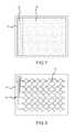
- FIGS. 5-8illustrate top views of an ITO patterned substrate 70 in various sequential stages of an exemplary manufacturing process.
- the substrate 70may be included in a touch screen sensor assembly (e.g., the touch screen sensor assembly 62 shown in FIGS. 3-4 ).
- a touch screen sensor assemblye.g., the touch screen sensor assembly 62 shown in FIGS. 3-4 .
- FIGS. 5-8similar or identical elements are indicated by the same reference numerals.
- FIG. 5shows the substrate 70 after it has been coated with an ITO layer 72 that has a relatively low surface resistivity (e.g., less than 20 Ohms, less than 10 Ohms, or the like).
- the ITO layer 72may be deposited onto the substrate 70 using any suitable process, such as vacuum sputtering. Although the ITO layer 72 is shown to be opaque, this is generally for illustrative purposes and it should be appreciated that the layer 72 may be somewhat transparent.
- the substratemay be formed from any suitable material, including glass, plastic (e.g., PET), or other material.
- FIG. 6illustrates the next step in the manufacturing process, which is to remove (e.g., by photo etching) the lower resistance ITO layer 72 off the portion of the substrate 70 that will overlay a display (indicated by the arrow 74 ).
- a section of the ITO layer 72is retained along one or more edges of the substrate 70 that will not overlay the display, and is used in a later step to form traces that function to couple the ITO electrodes to a controller.
- the ITO layer 72may be retained wherever it may be desirable to form conductive traces on the substrate 70 .
- the low resistance ITO layer 72may not be used in the viewing area because its transparency may be too low, such that the layer 72 would obstruct the view of an underlying display.
- FIG. 7illustrates the next step in the manufacturing process, which is to deposit (e.g., by vacuum sputtering) a relatively higher resistance ITO layer 76 onto the viewing portion of the substrate 70 .
- the ITO layer 76may have a surface resistivity of about 50 Ohms, 100 Ohms, 200 Ohms, or the like.
- the ITO layer 76may be relatively transparent, so that the view of a display associated with an assembled touch screen that includes the substrate 70 will not be obstructed.
- FIG. 8shows the substrate 70 after the next step in the manufacturing process, wherein a pattern of electrodes has been formed by etching (e.g., photo etching) the higher resistivity ITO layer 76 , and traces have been formed by etching the lower resistivity ITO layer 72 .
- the electrodes formed by the ITO layer 76may be coupled to a controller by the traces formed by the ITO layer 72 , which advantageously eliminates the need for metal traces.
- FIG. 8illustrates one example of a pattern of electrodes and traces, and that the manufacturing process described herein may be used to produce a substrate with any suitable pattern of electrodes and traces.
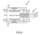
- FIG. 9illustrates the various layers that may be included in an exemplary touch screen sensor assembly 80 .
- the assembly 80includes a top substrate 82 a and a bottom substrate 82 b that are each coated with relatively high resistance ITO layers 84 a and 84 b (labeled ITO 1 ), respectively, that include a plurality of electrodes.
- the substrates 82 a and 82 bmay be configured from any suitable transparent material, including glass, plastic (e.g., PET), or the like.
- the top ITO layer 84 amay be separated from the bottom ITO layer 84 b by a suitable dielectric spacer 88 that is adhered by optically clear adhesive layers 86 a and 86 b.
- the ITO layers 84 a and 84 bmay be coupled to one or more controllers that are operable to excite and sense electrical signals on the electrodes of the ITO layers 84 a and 84 b .
- a flexible printed circuit (FPC) 96may be coupled to the assembly 80 .
- the FPC 96may include an FPC substrate 95 , top copper traces 94 a , and bottom copper traces 94 b , that are used to couple the top and bottom ITO layers 84 a and 84 b , respectively, to a controller.
- lower resistance ITO layers 90 a and 90 bmay be disposed in contact with portions of the ITO layers 84 a and 84 b . Further, the lower resistance ITO layers 90 a and 90 b may be coupled to the copper traces 94 a and 94 b using electrically conductive adhesive layers 92 a and 92 b , which may, for example, include an anisotropic conductive adhesive (ACA).
- ACAanisotropic conductive adhesive
- the lower resistance ITO layers 90 a - bare used for connection to the copper traces 94 a - b , as opposed to the higher resistance ITO layers 84 a - b , is that it may be desirable that the trace widths be relatively narrow, as narrow trace widths reduce the area required for the traces, and may also reduce the undesirable capacitance present in the traces.
- the relatively transparent ITO layer 84may have a high resistance, which would greatly reduce the performance of the touch screen sensor.
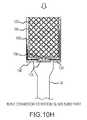
- FIGS. 10A-Hillustrate an exemplary manufacturing process for a touch screen sensor assembly including ITO layers having two different resistivities.
- the processmay be used to manufacture the touch screen sensor assembly 62 shown in FIGS. 3 and 4 .
- the touch screen sensor assemblymay include a bottom substrate 100 constructed from a suitable transparent material (e.g., glass, PET, or the like).
- the bottom substrate 100may be coated with a layer 102 of ITO (or other suitable material) having a relatively low resistivity (e.g., 50 Ohms/square, or the like) using a deposition process such as vacuum sputtering.
- the low resistivity ITO layer 102may be etched away from a viewing portion 104 of the bottom substrate 100 .
- the etchingmay be performed by any suitable layer removal process, such as photo etching, or the like.
- a high resistivity ITO layer 106may be deposited onto the viewing portion 104 of the bottom substrate 100 , as shown in FIG. 10C .
- a high resistivity ITO layer 122may be deposited onto a top substrate 120 .
- the high resistivity ITO layers 106 and 122may be more transparent than the low resistivity ITO layer 102 , such that a user may view a display that resides behind the viewing portion 104 of the assembled touch screen sensor assembly.
- FIG. 10Eillustrates the result after an etching process, wherein the high resistitivity ITO layer 106 has been etched into a pattern of electrodes. Further, the low resistitivity ITO layer 102 has been etched into a pattern of traces outside of the viewing portion 104 of the bottom substrate 100 .
- the pattern of traces etched from the low resistivity ITO layer 102includes a plurality of traces 103 and connection points 108 that are coupleable to electrodes formed by the high resistivity ITO layer 122 of the top substrate 120 when the touch screen sensor is assembled. Further, the traces etched from the ITO layer 102 include a portion 110 that operates to couple a connector to the traces (see FIG.
- FIG. 10Hillustrates the result after the high resistivity ITO layer 122 has been etched into a pattern of electrodes on the top substrate 120 .
- FIG. 10Gillustrates the result after the bottom substrate 100 and the top substrate 120 have been laminated together using a suitable optically clear adhesive (OCA).
- OCAoptically clear adhesive
- the “rows” of electrodes formed from the ITO layer 106 and the “columns” of electrodes formed from the ITO layer 122are aligned with each other to form a diamond pattern of electrodes that substantially covers the viewing portion of the touch screen sensor assembly.
- the electrodes formed from the ITO layer 122 of the top substrate 120are coupled to the traces 103 via the connection points 108 , such that the traces formed from the low resistivity ITO layer 102 may operate to couple the electrodes from both the top substrate 120 and the bottom substrate 100 to a controller and/or a computer system.
- FIG. 10Hillustrates the touch screen sensor assembly after a connector 130 (e.g., a flexible printed circuit connector) has been bonded to the bottom substrate 100 such that the traces formed from the ITO layer 102 are coupled to contacts of the connector 130 .
- the connector 130may be bonded to the bottom substrate 100 using any suitable adhesive, such as an anisotropic conductive film (ACF) or adhesive.
- ACFanisotropic conductive film
- the features described hereinoffer several advantages over previous designs. For example, in the case where metal traces are used, the manufacturing costs and complexity are high and environmental pollution may be a considerable problem. As another example, when silver conductive ink is printed for the traces, the trace height may be relatively large (e.g., greater than 10 um), the trace width must be relatively wide (e.g., greater than about 40 mm), and printing tolerances may be relatively large. Generally, a large trace height can cause unwanted bubbles to be formed when the top and bottom substrates are assembled together. By using a relatively low resistance ITO layer for the traces, the above-noted shortcomings are reduced or eliminated.
Landscapes
- Engineering & Computer Science (AREA)
- General Engineering & Computer Science (AREA)
- Theoretical Computer Science (AREA)
- Human Computer Interaction (AREA)
- Physics & Mathematics (AREA)
- General Physics & Mathematics (AREA)
- Manufacturing & Machinery (AREA)
- Microelectronics & Electronic Packaging (AREA)
- Position Input By Displaying (AREA)
Abstract
Description
Claims (16)
Priority Applications (1)
| Application Number | Priority Date | Filing Date | Title |
|---|---|---|---|
| US13/431,527US8507800B2 (en) | 2008-12-05 | 2012-03-27 | Capacitive touch panel having dual resistive layer |
Applications Claiming Priority (3)
| Application Number | Priority Date | Filing Date | Title |
|---|---|---|---|
| US12025408P | 2008-12-05 | 2008-12-05 | |
| US12/629,705US8209861B2 (en) | 2008-12-05 | 2009-12-02 | Method for manufacturing a touch screen sensor assembly |
| US13/431,527US8507800B2 (en) | 2008-12-05 | 2012-03-27 | Capacitive touch panel having dual resistive layer |
Related Parent Applications (1)
| Application Number | Title | Priority Date | Filing Date |
|---|---|---|---|
| US12/629,705DivisionUS8209861B2 (en) | 2008-12-05 | 2009-12-02 | Method for manufacturing a touch screen sensor assembly |
Publications (2)
| Publication Number | Publication Date |
|---|---|
| US20120181064A1 US20120181064A1 (en) | 2012-07-19 |
| US8507800B2true US8507800B2 (en) | 2013-08-13 |
Family
ID=42229806
Family Applications (2)
| Application Number | Title | Priority Date | Filing Date |
|---|---|---|---|
| US12/629,705Active2030-10-12US8209861B2 (en) | 2008-12-05 | 2009-12-02 | Method for manufacturing a touch screen sensor assembly |
| US13/431,527ActiveUS8507800B2 (en) | 2008-12-05 | 2012-03-27 | Capacitive touch panel having dual resistive layer |
Family Applications Before (1)
| Application Number | Title | Priority Date | Filing Date |
|---|---|---|---|
| US12/629,705Active2030-10-12US8209861B2 (en) | 2008-12-05 | 2009-12-02 | Method for manufacturing a touch screen sensor assembly |
Country Status (2)
| Country | Link |
|---|---|
| US (2) | US8209861B2 (en) |
| CN (1) | CN101819495B (en) |
Cited By (2)
| Publication number | Priority date | Publication date | Assignee | Title |
|---|---|---|---|---|
| WO2015164024A1 (en) | 2014-04-22 | 2015-10-29 | Carestream Health, Inc. | Laser patterning of dual sided transparent conductive films |
| US9280233B1 (en) | 2014-12-23 | 2016-03-08 | Synaptics Incorporated | Routing for touch sensor electrodes |
Families Citing this family (43)
| Publication number | Priority date | Publication date | Assignee | Title |
|---|---|---|---|---|
| TWI374379B (en) | 2007-12-24 | 2012-10-11 | Wintek Corp | Transparent capacitive touch panel and manufacturing method thereof |
| KR101076234B1 (en)* | 2009-02-13 | 2011-10-26 | 주식회사 포인칩스 | Touch screen input device |
| US8525809B2 (en)* | 2009-07-02 | 2013-09-03 | Applied Vacuum Coating Technologies Co., Ltd. | Digital capacitive touch panel structure |
| TW201102698A (en) | 2010-01-26 | 2011-01-16 | Mastouch Optoelectronics Technologies Co Ltd | Single-layer projected capacitive touch panel and fabricating method thereof |
| US9019233B2 (en) | 2010-01-26 | 2015-04-28 | Tpk Touch Solutions Inc. | Projected capacitive touch panel and method of manufacturing the same |
| TWM381837U (en)* | 2010-01-28 | 2010-06-01 | He Wei Technology Co Ltd | Touch control module |
| TWI471790B (en)* | 2010-02-03 | 2015-02-01 | Wintek Corp | Capacitive touch sensor and its fabrication method and capacitive touch panel |
| US8947399B2 (en)* | 2010-05-11 | 2015-02-03 | Tpk Touch Solutions Inc. | Dual-substrate capacitive touch panel |
| TW201102702A (en)* | 2010-05-11 | 2011-01-16 | Mastouch Optoelectronics Technologies Co Ltd | Capacitive touch panel |
| TW201145125A (en)* | 2010-06-03 | 2011-12-16 | J Touch Corp | Touch panel manufacturing method and structure thereof |
| CN102207805A (en)* | 2011-05-25 | 2011-10-05 | 赣州市德普特科技有限公司 | Capacitive touch screen and manufacture method thereof |
| EP2732361B1 (en)* | 2011-07-12 | 2018-05-23 | BlackBerry Limited | Electronic device and method of controlling a touch-sensitive display |
| US8337216B1 (en)* | 2011-07-26 | 2012-12-25 | Apple Inc. | Touch sensor back plane ground connection |
| DE102011111506B4 (en)* | 2011-08-31 | 2017-05-18 | Leonhard Kurz Stiftung & Co. Kg | Plastic film and touch sensor |
| WO2013049816A1 (en) | 2011-09-30 | 2013-04-04 | Sensitronics, LLC | Hybrid capacitive force sensors |
| TW201332782A (en)* | 2011-10-25 | 2013-08-16 | Unipixel Displays Inc | Method of manufacturing a capacative touch sensor circuit using flexographic printing |
| KR20140096306A (en)* | 2011-10-25 | 2014-08-05 | 유니-픽셀 디스플레이스, 인코포레이티드 | Method of manufacturing a resistive touch sensor circuit by flexographic printing |
| CN103123547A (en)* | 2011-11-16 | 2013-05-29 | 宸鸿科技(厦门)有限公司 | Piling structure of optics panel and manufacturing method thereof |
| KR101357586B1 (en)* | 2012-01-18 | 2014-02-05 | 엘지이노텍 주식회사 | Touch panel |
| NL2008182C2 (en)* | 2012-01-26 | 2013-07-29 | Dennis Smalbrugge | CONTROL DEVICE, CONTROL ELEMENT AND METHOD FOR GENERATING AN INPUT SIGNAL. |
| US20130206566A1 (en)* | 2012-02-15 | 2013-08-15 | Chih-Chung Lin | Capacitive touch device |
| TW201340181A (en) | 2012-03-30 | 2013-10-01 | Chunghwa Picture Tubes Ltd | Touch panel and method for manufacturing a touch sensor of the touch panel |
| US20130264184A1 (en)* | 2012-04-10 | 2013-10-10 | Chih-Chung Lin | Capacitive touch device |
| US9164548B2 (en)* | 2012-04-13 | 2015-10-20 | Htc Corporation | Touch panel and handheld electronic device utilizing the same |
| TWI566153B (en)* | 2012-07-10 | 2017-01-11 | 元太科技工業股份有限公司 | Touch panel and manufacturing method thereof and touch display panel |
| CN103687343A (en)* | 2012-09-04 | 2014-03-26 | 苏州点精光电有限公司 | Method for manufacturing structural-stacked type printed circuit board |
| CN103906374B (en)* | 2012-12-28 | 2017-02-15 | 富葵精密组件(深圳)有限公司 | rigid-flexible combined board and manufacturing method thereof |
| US9974163B2 (en)* | 2012-12-28 | 2018-05-15 | Futurewei Technologies, Inc. | Miniature high density opto-electronic package |
| WO2014123431A2 (en)* | 2013-02-07 | 2014-08-14 | Stretchsense Limited | Method and apparatus for attaching a soft and flexible circuit to a connector |
| US9448666B2 (en)* | 2013-06-08 | 2016-09-20 | Microsoft Technology Licensing, Llc | Dark film lamination for a touch sensor |
| CN103455224A (en)* | 2013-08-09 | 2013-12-18 | 东莞市胜大光电科技有限公司 | Capacitive OGS substrate touch screen production process |
| US9782955B2 (en) | 2013-09-24 | 2017-10-10 | 3M Innovative Properties Company | Transferable transparent conductive patterns and display stack materials |
| CN103713790A (en)* | 2013-11-18 | 2014-04-09 | 江西合力泰科技股份有限公司 | Method for manufacturing OGS (one glass solution) touch screen by means of electroplating BM (black matrix) on front surface thereof |
| US20150199048A1 (en)* | 2014-01-15 | 2015-07-16 | Carestream Health, Inc. | Touch panel assembly |
| CN104966551A (en)* | 2015-05-30 | 2015-10-07 | 汕头万顺包装材料股份有限公司 | ITO conductive film with copper-plated surface |
| CN106502480A (en)* | 2015-09-08 | 2017-03-15 | 深圳安道云科股份有限公司 | A kind of manufacture method of oversize capacitive touch screen |
| MX381491B (en)* | 2016-04-13 | 2025-03-12 | Tactotek Oy | Multilayer structure with embedded multilayer electronics |
| US10236240B2 (en) | 2016-05-11 | 2019-03-19 | Advanced Semiconductor Engineering, Inc. | Low loss substrate for high data rate applications |
| US10120514B2 (en)* | 2016-06-24 | 2018-11-06 | Stmicroelectronics Asia Pacific Pte Ltd | Capacitive touch pressure sensor constructed from flexible substrate |
| US10684734B2 (en)* | 2017-09-28 | 2020-06-16 | Apple Inc. | Transparent high-resistivity layer for electrostatic friction modulation over a capacitive input sensor |
| CN109375838A (en)* | 2018-11-16 | 2019-02-22 | 深圳晶华显示器材有限公司 | a touch screen |
| CN111625143B (en)* | 2020-05-26 | 2024-04-12 | 京东方科技集团股份有限公司 | Touch control substrate and manufacturing method thereof |
| US12130977B2 (en)* | 2023-03-27 | 2024-10-29 | Cirque Corporation | Pressure capacitive reference fixed to a housing |
Citations (178)
| Publication number | Priority date | Publication date | Assignee | Title |
|---|---|---|---|---|
| US4550221A (en) | 1983-10-07 | 1985-10-29 | Scott Mabusth | Touch sensitive control device |
| US5062198A (en) | 1990-05-08 | 1991-11-05 | Keytec, Inc. | Method of making a transparent touch screen switch assembly |
| US5379057A (en) | 1988-11-14 | 1995-01-03 | Microslate, Inc. | Portable computer with touch screen and computer system employing same |
| US5459463A (en) | 1990-05-25 | 1995-10-17 | Sextant Avionique | Device for locating an object situated close to a detection area and a transparent keyboard using said device |
| US5488204A (en) | 1992-06-08 | 1996-01-30 | Synaptics, Incorporated | Paintbrush stylus for capacitive touch sensor pad |
| US5495077A (en) | 1992-06-08 | 1996-02-27 | Synaptics, Inc. | Object position and proximity detector |
| US5543590A (en) | 1992-06-08 | 1996-08-06 | Synaptics, Incorporated | Object position detector with edge motion feature |
| US5543592A (en) | 1993-07-23 | 1996-08-06 | Sextant Avionique | Multimode manipulator |
| US5543588A (en) | 1992-06-08 | 1996-08-06 | Synaptics, Incorporated | Touch pad driven handheld computing device |
| US5650597A (en) | 1995-01-20 | 1997-07-22 | Dynapro Systems, Inc. | Capacitive touch sensor |
| US5730165A (en) | 1995-12-26 | 1998-03-24 | Philipp; Harald | Time domain capacitive field detector |
| US5825352A (en) | 1996-01-04 | 1998-10-20 | Logitech, Inc. | Multiple fingers contact sensing method for emulating mouse buttons and mouse operations on a touch sensor pad |
| US5854625A (en) | 1996-11-06 | 1998-12-29 | Synaptics, Incorporated | Force sensing touchpad |
| US5854450A (en) | 1995-04-19 | 1998-12-29 | Elo Touchsystems, Inc. | Acoustic condition sensor employing a plurality of mutually non-orthogonal waves |
| US5861583A (en) | 1992-06-08 | 1999-01-19 | Synaptics, Incorporated | Object position detector |
| US5880411A (en) | 1992-06-08 | 1999-03-09 | Synaptics, Incorporated | Object position detector with edge motion feature and gesture recognition |
| US5920310A (en) | 1996-11-15 | 1999-07-06 | Synaptics, Incorporated | Electronic device employing a touch sensitive transducer |
| US5940065A (en) | 1996-03-15 | 1999-08-17 | Elo Touchsystems, Inc. | Algorithmic compensation system and method therefor for a touch sensor panel |
| US5943052A (en) | 1997-08-12 | 1999-08-24 | Synaptics, Incorporated | Method and apparatus for scroll bar control |
| US6091406A (en) | 1996-12-25 | 2000-07-18 | Elo Touchsystems, Inc. | Grating transducer for acoustic touchscreens |
| US6188391B1 (en) | 1998-07-09 | 2001-02-13 | Synaptics, Inc. | Two-layer capacitive touchpad and method of making same |
| US6236391B1 (en) | 1995-01-24 | 2001-05-22 | Elo Touchsystems, Inc. | Acoustic touch position sensor using a low acoustic loss transparent substrate |
| KR200229845Y1 (en) | 2001-02-23 | 2001-07-19 | 주식회사 에이터치 | Structure of Contact of Substrate in Touch Screen |
| US6288707B1 (en) | 1996-07-29 | 2001-09-11 | Harald Philipp | Capacitive position sensor |
| US6297811B1 (en) | 1999-06-02 | 2001-10-02 | Elo Touchsystems, Inc. | Projective capacitive touchscreen |
| US20010026330A1 (en) | 2000-03-28 | 2001-10-04 | Oh Hyeok-Jin | Liquid crystal display employing touch panel |
| US20020030666A1 (en) | 1999-01-25 | 2002-03-14 | Harald Philipp | Capacitive position sensor |
| US6373474B1 (en) | 1998-10-27 | 2002-04-16 | Pentel Kabushiki Kaisha | Real contact type touch panel apparatus |
| US6380929B1 (en) | 1996-09-20 | 2002-04-30 | Synaptics, Incorporated | Pen drawing computer input device |
| US6379509B2 (en) | 1998-01-20 | 2002-04-30 | 3M Innovative Properties Company | Process for forming electrodes |
| US6441809B2 (en) | 1995-01-24 | 2002-08-27 | Elo Touchsystems, Inc. | Acoustic touch position sensor using a low acoustic loss transparent substrate |
| US6452514B1 (en) | 1999-01-26 | 2002-09-17 | Harald Philipp | Capacitive sensor and array |
| US20020145593A1 (en) | 2001-04-06 | 2002-10-10 | 3M Innovative Properties Company | Frontlit illuminated touch panel |
| US6466036B1 (en) | 1998-11-25 | 2002-10-15 | Harald Philipp | Charge transfer capacitance measurement circuit |
| US6488981B1 (en) | 2001-06-20 | 2002-12-03 | 3M Innovative Properties Company | Method of manufacturing a touch screen panel |
| US6492979B1 (en) | 1999-09-07 | 2002-12-10 | Elo Touchsystems, Inc. | Dual sensor touchscreen utilizing projective-capacitive and force touch sensors |
| US20020191029A1 (en) | 2001-05-16 | 2002-12-19 | Synaptics, Inc. | Touch screen with user interface enhancement |
| US6504583B2 (en) | 1998-10-02 | 2003-01-07 | 3M Innovative Properties Company | Anti-microbial touch panel and method of making same using homeotropic liquid crystal silanes |
| US6504530B1 (en) | 1999-09-07 | 2003-01-07 | Elo Touchsystems, Inc. | Touch confirming touchscreen utilizing plural touch sensors |
| US6549193B1 (en) | 1998-10-09 | 2003-04-15 | 3M Innovative Properties Company | Touch panel with improved linear response and minimal border width electrode pattern |
| US6555235B1 (en) | 2000-07-06 | 2003-04-29 | 3M Innovative Properties Co. | Touch screen system |
| US20030095111A1 (en) | 2001-11-14 | 2003-05-22 | In-Duk Song | Touch panel |
| US20030103043A1 (en) | 2001-11-30 | 2003-06-05 | 3M Innovative Properties Company | System and method for locating a touch on a capacitive touch screen |
| US6587097B1 (en) | 2000-11-28 | 2003-07-01 | 3M Innovative Properties Co. | Display system |
| US20030132922A1 (en) | 2002-01-17 | 2003-07-17 | Harald Philipp | Touch screen detection apparatus |
| US20030184523A1 (en) | 2002-03-29 | 2003-10-02 | 3M Innovative Properties Company | Moisture deflector for capacitive NFI touch screens for use with bezels of conductive material |
| US20030205450A1 (en) | 2002-05-02 | 2003-11-06 | 3M Innovative Properties Company | Pressure activated switch and touch panel |
| US20040008129A1 (en) | 2002-07-12 | 2004-01-15 | Harald Philipp | Keyboard with reduced keying ambiguity |
| US20040061687A1 (en) | 2002-09-17 | 2004-04-01 | Elo Touchsystems, Inc. | Dynamic corrections for a non-linear touchscreen |
| US20040095336A1 (en)* | 2002-11-20 | 2004-05-20 | Hong Hee Jung | Digital resistive-type touch panel |
| US20040100448A1 (en) | 2002-11-25 | 2004-05-27 | 3M Innovative Properties Company | Touch display |
| US20040104826A1 (en) | 2002-10-31 | 2004-06-03 | Harald Philipp | Charge transfer capacitive position sensor |
| US20040135773A1 (en) | 2002-12-24 | 2004-07-15 | Bang Yong Ik | Touch panel integrated with liquid crystal display |
| US6784873B1 (en) | 2000-08-04 | 2004-08-31 | Peter V. Boesen | Method and medium for computer readable keyboard display incapable of user termination |
| US20040188150A1 (en) | 2003-03-25 | 2004-09-30 | 3M Innovative Properties Company | High transparency touch screen |
| US20040189882A1 (en) | 1999-04-13 | 2004-09-30 | Jeong Yun Cheol | Polarizer integrated with transparent conductive film, a touch panel integrated with the polarizer and a flat panel display integrated with the touch panel |
| JP2004280720A (en) | 2003-03-18 | 2004-10-07 | Kawaguchiko Seimitsu Co Ltd | Touch panel and screen input type display device provided with it |
| US6819316B2 (en) | 2001-04-17 | 2004-11-16 | 3M Innovative Properties Company | Flexible capacitive touch sensor |
| US20040252109A1 (en) | 2002-04-11 | 2004-12-16 | Synaptics, Inc. | Closed-loop sensor on a solid-state object position detector |
| US20050024341A1 (en) | 2001-05-16 | 2005-02-03 | Synaptics, Inc. | Touch screen with user interface enhancement |
| US6856259B1 (en) | 2004-02-06 | 2005-02-15 | Elo Touchsystems, Inc. | Touch sensor system to detect multiple touch events |
| US20050035953A1 (en) | 2003-06-20 | 2005-02-17 | Richard Woolley | Single-layer touchpad and methods of use |
| US20050041018A1 (en) | 2003-08-21 | 2005-02-24 | Harald Philipp | Anisotropic touch screen element |
| US20050052429A1 (en) | 2003-08-21 | 2005-03-10 | Harald Philipp | Capacitive position sensor |
| US20050078027A1 (en) | 2003-10-08 | 2005-04-14 | Harald Philipp | Touch sensitive control panel |
| US20050110766A1 (en) | 2003-11-24 | 2005-05-26 | Elo Touchsystems, Inc. | Touch sensor with conductive polymer switches |
| US20050110767A1 (en) | 2003-11-24 | 2005-05-26 | Elo Touchsystems, Inc. | Method of manufacturing touch sensor with switch tape strips |
| US6904570B2 (en) | 2001-06-07 | 2005-06-07 | Synaptics, Inc. | Method and apparatus for controlling a display of data on a display screen |
| US20050162408A1 (en) | 2004-01-27 | 2005-07-28 | Elo Touchsystems, Inc. | Capacitive touch sensor |
| US20050174335A1 (en) | 2004-02-10 | 2005-08-11 | Elo Touchsystems, Inc. | Resistive touchscreen with programmable display coversheet |
| US20050179673A1 (en) | 2004-02-13 | 2005-08-18 | Harald Philipp | Capacitive sensor |
| US6943705B1 (en) | 2002-05-03 | 2005-09-13 | Synaptics, Inc. | Method and apparatus for providing an integrated membrane switch and capacitive sensor |
| US6961049B2 (en) | 2002-06-21 | 2005-11-01 | 3M Innovative Properties Company | Capacitive touch sensor architecture with unique sensor bar addressing |
| US20050246459A1 (en) | 2003-07-11 | 2005-11-03 | Harald Philipp | Keyboard With Reduced Keying Ambiguity |
| US20050260338A1 (en) | 2004-05-19 | 2005-11-24 | Trendon Touch Technology Corp. | Method of manufacturing circuit layout on touch panel by utilizing metal plating technology |
| US6970160B2 (en) | 2002-12-19 | 2005-11-29 | 3M Innovative Properties Company | Lattice touch-sensing system |
| US6977646B1 (en) | 2001-11-30 | 2005-12-20 | 3M Innovative Properties Co. | Touch screen calibration system and method |
| US7000474B2 (en) | 2003-02-28 | 2006-02-21 | Elo Touchsystems, Inc. | Acoustic device using higher order harmonic piezoelectric element |
| US7006081B2 (en) | 2000-10-20 | 2006-02-28 | Elo Touchsystems, Inc. | Acoustic touch sensor with laminated substrate |
| US7030860B1 (en) | 1999-10-08 | 2006-04-18 | Synaptics Incorporated | Flexible transparent touch sensing system for electronic devices |
| US20060097991A1 (en) | 2004-05-06 | 2006-05-11 | Apple Computer, Inc. | Multipoint touchscreen |
| US20060132462A1 (en) | 2004-12-22 | 2006-06-22 | 3M Innovative Properties Company | Touch sensors incorporating capacitively coupled electrodes |
| US20060139340A1 (en) | 2001-10-03 | 2006-06-29 | 3M Innovative Properties Company | Touch panel system and method for distinguishing multiple touch inputs |
| US20060187214A1 (en) | 1992-06-08 | 2006-08-24 | Synaptics, Inc, A California Corporation | Object position detector with edge motion feature and gesture recognition |
| US20060192690A1 (en) | 2002-07-12 | 2006-08-31 | Harald Philipp | Capacitive Keyboard with Non-Locking Reduced Keying Ambiguity |
| US7102621B2 (en) | 1997-09-30 | 2006-09-05 | 3M Innovative Properties Company | Force measurement system correcting for inertial interference |
| US20060202970A1 (en) | 2005-03-11 | 2006-09-14 | Jia-Yih Lii | Touchpad with single-layered printed circuit board structure |
| US7109976B2 (en) | 2003-04-01 | 2006-09-19 | 3M Innovative Properties Company | Display screen seal |
| CN1838151A (en) | 2005-03-22 | 2006-09-27 | 义隆电子股份有限公司 | Single-layer printed circuit board structure touch panel |
| US20060238513A1 (en) | 2004-05-21 | 2006-10-26 | Harald Philipp | Touch sensitive control panel |
| US7129935B2 (en) | 2003-06-02 | 2006-10-31 | Synaptics Incorporated | Sensor patterns for a capacitive sensing apparatus |
| US20060274055A1 (en) | 2005-06-01 | 2006-12-07 | Synaptics Incorporated | Touch pad with flexible substrate |
| US20060274047A1 (en) | 2005-06-02 | 2006-12-07 | Eastman Kodak Company | Touchscreen with one carbon nanotube conductive layer |
| US7148882B2 (en) | 2003-05-16 | 2006-12-12 | 3M Innovatie Properties Company | Capacitor based force sensor |
| US7151532B2 (en) | 2002-08-09 | 2006-12-19 | 3M Innovative Properties Company | Multifunctional multilayer optical film |
| US20060284836A1 (en) | 2005-06-17 | 2006-12-21 | Harald Philipp | Control Panel |
| US7154481B2 (en) | 2002-06-25 | 2006-12-26 | 3M Innovative Properties Company | Touch sensor |
| US7158122B2 (en) | 2002-05-17 | 2007-01-02 | 3M Innovative Properties Company | Calibration of force based touch panel systems |
| US20070002192A1 (en) | 2005-06-29 | 2007-01-04 | Casio Computer Co., Ltd. | Liquid crystal display apparatus including touch panel |
| US20070008299A1 (en) | 2005-07-08 | 2007-01-11 | Harald Philipp | Two-Dimensional Position Sensor |
| US20070026089A1 (en) | 2005-07-29 | 2007-02-01 | Trendon Touch Technology Corp. | Touch screen with bacteria inhibition layer and manufacturing method thereof |
| US7176902B2 (en) | 2003-10-10 | 2007-02-13 | 3M Innovative Properties Company | Wake-on-touch for vibration sensing touch input devices |
| US7176897B2 (en) | 2002-05-17 | 2007-02-13 | 3M Innovative Properties Company | Correction of memory effect errors in force-based touch panel systems |
| US7183948B2 (en) | 2001-04-13 | 2007-02-27 | 3M Innovative Properties Company | Tangential force control in a touch location device |
| US7190352B2 (en) | 2002-10-31 | 2007-03-13 | Ownway Biotronics Inc. | Method and apparatus of electrotactile panel with pointing system |
| US7190350B2 (en) | 2001-04-13 | 2007-03-13 | 3M Innovative Properties Company | Touch screen with rotationally isolated force sensor |
| US20070062739A1 (en) | 2005-09-20 | 2007-03-22 | Harald Philipp | Touch Sensitive Screen |
| US20070074914A1 (en) | 2005-10-05 | 2007-04-05 | Geaghan Bernard O | Interleaved electrodes for touch sensing |
| US7202859B1 (en) | 2002-08-09 | 2007-04-10 | Synaptics, Inc. | Capacitive sensing pattern |
| US20070085838A1 (en) | 2005-10-17 | 2007-04-19 | Ricks Theodore K | Method for making a display with integrated touchscreen |
| US7212189B2 (en) | 1999-11-04 | 2007-05-01 | Synaptics Incorporated | Capacitive mouse |
| US20070103446A1 (en) | 2005-11-04 | 2007-05-10 | Trendon Touch Technology Corp. | Wiring of touch panel |
| US20070109274A1 (en) | 2005-11-15 | 2007-05-17 | Synaptics Incorporated | Methods and systems for detecting a position-based attribute of an object using digital codes |
| US7227538B2 (en) | 2004-02-25 | 2007-06-05 | 3M Innovative Properties Company | Touch sensor with linearized response |
| US7236161B2 (en) | 2003-03-21 | 2007-06-26 | 3M Innovative Properties Company | Remote touch simulation systems and methods |
| US20070159561A1 (en) | 2006-01-10 | 2007-07-12 | Trendon Touch Technology Corp. | Display panel having touching circuit |
| US20070176906A1 (en) | 2006-02-01 | 2007-08-02 | Synaptics Incorporated | Proximity sensor and method for indicating extended interface results |
| US7253643B1 (en) | 2006-07-19 | 2007-08-07 | Cypress Semiconductor Corporation | Uninterrupted radial capacitive sense interface |
| US20070222766A1 (en) | 2006-03-24 | 2007-09-27 | Synaptics Incorporated | Touch sensor effective area enhancement |
| US7277087B2 (en) | 2003-12-31 | 2007-10-02 | 3M Innovative Properties Company | Touch sensing with touch down and lift off sensitivity |
| US20070229466A1 (en) | 2006-03-30 | 2007-10-04 | Cypress Semiconductor Corporation | Apparatus and method for recognizing a tap gesture on a touch sensing device |
| US20070229470A1 (en) | 2006-03-31 | 2007-10-04 | Warren Snyder | Capacitive touch sense device having polygonal shaped sensor elements |
| US20070229468A1 (en) | 2006-03-30 | 2007-10-04 | Cypress Semiconductor Corporation | Apparatus and method for reducing average scan rate to detect a conductive object on a sensing device |
| US20070236475A1 (en) | 2006-04-05 | 2007-10-11 | Synaptics Incorporated | Graphical scroll wheel |
| US20070236618A1 (en) | 2006-03-31 | 2007-10-11 | 3M Innovative Properties Company | Touch Screen Having Reduced Visibility Transparent Conductor Pattern |
| US20070247443A1 (en) | 2006-04-25 | 2007-10-25 | Harald Philipp | Hybrid Capacitive Touch Screen Element |
| US20070257893A1 (en) | 2006-05-02 | 2007-11-08 | Harald Philipp | Touch Screen |
| US20070257894A1 (en) | 2006-05-05 | 2007-11-08 | Harald Philipp | Touch Screen Element |
| US20070264844A1 (en) | 2006-05-10 | 2007-11-15 | Trendon Touch Technology Corp. | Method of hiding transparent electrodes on a transparent substrate |
| US20070262962A1 (en) | 2006-05-10 | 2007-11-15 | Cypress Semiconductor Corporation | Apparatus and method for reducing charge time and power consumption of a sensing device |
| US20070262963A1 (en) | 2006-05-11 | 2007-11-15 | Cypress Semiconductor Corporation | Apparatus and method for recognizing a button operation on a sensing device |
| US7298367B2 (en) | 2003-11-25 | 2007-11-20 | 3M Innovative Properties Company | Light emitting stylus and user input device using same |
| US20070268276A1 (en) | 2003-06-24 | 2007-11-22 | Kent Joel C | Acoustic Touch Sensor with Low Profile Diffractive Grating Transducer Assembly |
| US20070268265A1 (en) | 2006-05-18 | 2007-11-22 | Cypress Semiconductor Corporation | Two-pin buttons |
| US20070268266A1 (en) | 2006-05-18 | 2007-11-22 | Cypress Semiconductor Corporation | Toothed slider |
| US20070273561A1 (en) | 2006-05-25 | 2007-11-29 | Harald Philipp | Capacitive Keyboard with Position Dependent Reduced Keying Ambiguity |
| US20070273560A1 (en) | 2006-05-25 | 2007-11-29 | Cypress Semiconductor Corporation | Low pin count solution using capacitance sensing matrix for keyboard architecture |
| US20070279395A1 (en) | 2006-05-31 | 2007-12-06 | Harald Philipp | Two Dimensional Position Sensor |
| US7307624B2 (en) | 2003-12-30 | 2007-12-11 | 3M Innovative Properties Company | Touch sensor with linearized response |
| US20070291009A1 (en) | 2006-06-19 | 2007-12-20 | Cypress Semiconductor Corporation | Apparatus and method for detecting a touch-sensor pad gesture |
| US20070291016A1 (en) | 2006-06-20 | 2007-12-20 | Harald Philipp | Capacitive Position Sensor |
| US20070296709A1 (en) | 2006-06-27 | 2007-12-27 | Cypress Semiconductor Corporation | Apparatus and method for detecting multiple buttons with one pin |
| US7315300B2 (en) | 2003-12-31 | 2008-01-01 | 3M Innovative Properties Company | Touch sensitive device employing impulse reconstruction |
| US20080001925A1 (en) | 2006-06-30 | 2008-01-03 | Cypress Semiconductor Corporation | Navigation panel |
| US20080007434A1 (en) | 2006-07-10 | 2008-01-10 | Luben Hristov | Priority and Combination Suppression Techniques (PST/CST) for a Capacitive Keyboard |
| US20080007534A1 (en) | 2006-07-10 | 2008-01-10 | Cypress Semiconductor Corporation | Touch-sensor with shared capacitive sensors |
| US20080012832A1 (en) | 2006-07-13 | 2008-01-17 | Guanghai Li | Multi-function touchpad |
| US20080024461A1 (en) | 2003-12-15 | 2008-01-31 | 3M Innovative Properties Company | Wiring harness and touch sensor incorporating same |
| US7327352B2 (en) | 2002-06-14 | 2008-02-05 | 3M Innovative Properties Company | Linearized conductive surface |
| US20080029292A1 (en) | 2004-04-20 | 2008-02-07 | Ryuji Takayama | Transparent Conductive Formed Article for a Touch Panel and Touch Panel |
| CN101122839A (en) | 2007-10-11 | 2008-02-13 | 友达光电股份有限公司 | Capacitive touch pad with low impedance structure and manufacturing method thereof |
| US20080048997A1 (en) | 1992-06-08 | 2008-02-28 | Synaptics Incorporated | Object position detector with edge motion feature and gesture recognition |
| US20080062139A1 (en) | 2006-06-09 | 2008-03-13 | Apple Inc. | Touch screen liquid crystal display |
| US20080074398A1 (en) | 2006-09-26 | 2008-03-27 | David Gordon Wright | Single-layer capacitive sensing device |
| US20080111714A1 (en) | 2006-11-14 | 2008-05-15 | Viktor Kremin | Capacitance to code converter with sigma-delta modulator |
| US20080122802A1 (en) | 2006-11-29 | 2008-05-29 | Tsutomu Furuhashi | Liquid crystal dispaly device with touch screen |
| US20080138589A1 (en) | 2005-05-26 | 2008-06-12 | Gunze Limited | Transparent Planar Body and Transparent Touch Switch |
| US20080142352A1 (en) | 2006-12-18 | 2008-06-19 | Wright David G | Two circuit board touch-sensor device |
| US20080143683A1 (en) | 2006-12-15 | 2008-06-19 | Apple Inc. | Pet-based touch pad |
| US20080150906A1 (en) | 2006-12-22 | 2008-06-26 | Grivna Edward L | Multi-axial touch-sensor device with multi-touch resolution |
| US20080150905A1 (en) | 2006-12-21 | 2008-06-26 | Grivna Edward L | Feedback mechanism for user detection of reference location on a sensing device |
| US20080158183A1 (en) | 2007-01-03 | 2008-07-03 | Apple Computer, Inc. | Double-sided touch-sensitive panel with shield and drive combined layer |
| US20080158181A1 (en) | 2007-01-03 | 2008-07-03 | Apple Computer, Inc. | Double-sided touch sensitive panel and flex circuit bonding |
| US20080165139A1 (en) | 2007-01-05 | 2008-07-10 | Apple Inc. | Touch screen stack-up processing |
| US20080165158A1 (en) | 2007-01-05 | 2008-07-10 | Apple Inc. | Touch screen stack-ups |
| US20080264699A1 (en) | 2007-04-27 | 2008-10-30 | Trendon Touch Technology Corp. | Conductor pattern structure of capacitive touch panel |
| US20080309635A1 (en) | 2007-06-14 | 2008-12-18 | Epson Imaging Devices Corporation | Capacitive input device |
| US20090085891A1 (en) | 2007-09-29 | 2009-04-02 | Au Optronics Corporation | Capacitive Touch Panel with Low Impedance |
| US20090160824A1 (en) | 2007-12-25 | 2009-06-25 | Cando Corporation | Sensory structure of touch panel |
| US20090167710A1 (en) | 2007-12-27 | 2009-07-02 | Tsinghua University | Touch panel and display device using the same |
| KR100907512B1 (en) | 2006-12-29 | 2009-07-14 | (주)탑나노시스 | Method of forming a touch panel and a conductive layer of the touch panel |
| US20090194344A1 (en) | 2008-01-31 | 2009-08-06 | Avago Technologies Ecbu Ip (Singapore) Pte. Ltd. | Single Layer Mutual Capacitance Sensing Systems, Device, Components and Methods |
| US20090236151A1 (en) | 2008-03-21 | 2009-09-24 | I-Hau Yeh | Touch Panel Device |
| US20090309850A1 (en) | 2008-06-16 | 2009-12-17 | Kai-Ti Yang | Capacitive touch panel |
| US20100045625A1 (en) | 2008-08-21 | 2010-02-25 | Tpo Displays Corp. | Touch panel and system for displaying images utilizing the same |
| US20100066700A1 (en) | 2008-09-12 | 2010-03-18 | Ocular Lcd Inc. | Capacitive Touch Screen |
| US20100073319A1 (en) | 2008-09-25 | 2010-03-25 | Apple Inc. | Capacitive sensor having electrodes arranged on the substrate and the flex circuit |
| US7945297B2 (en) | 2005-09-30 | 2011-05-17 | Atmel Corporation | Headsets and headset power management |
- 2009
- 2009-12-02USUS12/629,705patent/US8209861B2/enactiveActive
- 2009-12-07CNCN200910266595.4Apatent/CN101819495B/enactiveActive
- 2012
- 2012-03-27USUS13/431,527patent/US8507800B2/enactiveActive
Patent Citations (229)
| Publication number | Priority date | Publication date | Assignee | Title |
|---|---|---|---|---|
| US4550221A (en) | 1983-10-07 | 1985-10-29 | Scott Mabusth | Touch sensitive control device |
| US5675362A (en) | 1988-11-14 | 1997-10-07 | Microslate, Inc. | Portable computer with touch screen and computing system employing same |
| US5379057A (en) | 1988-11-14 | 1995-01-03 | Microslate, Inc. | Portable computer with touch screen and computer system employing same |
| US5062198A (en) | 1990-05-08 | 1991-11-05 | Keytec, Inc. | Method of making a transparent touch screen switch assembly |
| US5459463A (en) | 1990-05-25 | 1995-10-17 | Sextant Avionique | Device for locating an object situated close to a detection area and a transparent keyboard using said device |
| US5495077A (en) | 1992-06-08 | 1996-02-27 | Synaptics, Inc. | Object position and proximity detector |
| US20080042994A1 (en) | 1992-06-08 | 2008-02-21 | Synaptics Incorporated | Object position detector with edge motion feature and gesture recognition |
| US6414671B1 (en) | 1992-06-08 | 2002-07-02 | Synaptics Incorporated | Object position detector with edge motion feature and gesture recognition |
| US5543588A (en) | 1992-06-08 | 1996-08-06 | Synaptics, Incorporated | Touch pad driven handheld computing device |
| US20060092142A1 (en) | 1992-06-08 | 2006-05-04 | Synaptics, Inc., A California Corporation | Object position detector with edge motion feature and gesture recognition |
| US6380931B1 (en) | 1992-06-08 | 2002-04-30 | Synaptics Incorporated | Object position detector with edge motion feature and gesture recognition |
| US20040178997A1 (en) | 1992-06-08 | 2004-09-16 | Synaptics, Inc., A California Corporation | Object position detector with edge motion feature and gesture recognition |
| US6750852B2 (en) | 1992-06-08 | 2004-06-15 | Synaptics, Inc. | Object position detector with edge motion feature and gesture recognition |
| US5841078A (en) | 1992-06-08 | 1998-11-24 | Synaptics, Inc. | Object position detector |
| US5543590A (en) | 1992-06-08 | 1996-08-06 | Synaptics, Incorporated | Object position detector with edge motion feature |
| US20080048997A1 (en) | 1992-06-08 | 2008-02-28 | Synaptics Incorporated | Object position detector with edge motion feature and gesture recognition |
| US5861583A (en) | 1992-06-08 | 1999-01-19 | Synaptics, Incorporated | Object position detector |
| US5880411A (en) | 1992-06-08 | 1999-03-09 | Synaptics, Incorporated | Object position detector with edge motion feature and gesture recognition |
| US5488204A (en) | 1992-06-08 | 1996-01-30 | Synaptics, Incorporated | Paintbrush stylus for capacitive touch sensor pad |
| US7109978B2 (en) | 1992-06-08 | 2006-09-19 | Synaptics, Inc. | Object position detector with edge motion feature and gesture recognition |
| US20060187214A1 (en) | 1992-06-08 | 2006-08-24 | Synaptics, Inc, A California Corporation | Object position detector with edge motion feature and gesture recognition |
| US5543592A (en) | 1993-07-23 | 1996-08-06 | Sextant Avionique | Multimode manipulator |
| US5650597A (en) | 1995-01-20 | 1997-07-22 | Dynapro Systems, Inc. | Capacitive touch sensor |
| US6441809B2 (en) | 1995-01-24 | 2002-08-27 | Elo Touchsystems, Inc. | Acoustic touch position sensor using a low acoustic loss transparent substrate |
| US6236391B1 (en) | 1995-01-24 | 2001-05-22 | Elo Touchsystems, Inc. | Acoustic touch position sensor using a low acoustic loss transparent substrate |
| US5854450A (en) | 1995-04-19 | 1998-12-29 | Elo Touchsystems, Inc. | Acoustic condition sensor employing a plurality of mutually non-orthogonal waves |
| US7061475B2 (en) | 1995-04-19 | 2006-06-13 | Elo Touchsystems, Inc. | Acoustic condition sensor employing a plurality of mutually non-orthogonal waves |
| US6723929B2 (en) | 1995-04-19 | 2004-04-20 | Elo Touchsystems, Inc. | Acoustic condition sensor employing a plurality of mutually non-orthogonal waves |
| US5730165A (en) | 1995-12-26 | 1998-03-24 | Philipp; Harald | Time domain capacitive field detector |
| US5825352A (en) | 1996-01-04 | 1998-10-20 | Logitech, Inc. | Multiple fingers contact sensing method for emulating mouse buttons and mouse operations on a touch sensor pad |
| US6506983B1 (en) | 1996-03-15 | 2003-01-14 | Elo Touchsystems, Inc. | Algorithmic compensation system and method therefor for a touch sensor panel |
| US5940065A (en) | 1996-03-15 | 1999-08-17 | Elo Touchsystems, Inc. | Algorithmic compensation system and method therefor for a touch sensor panel |
| US6288707B1 (en) | 1996-07-29 | 2001-09-11 | Harald Philipp | Capacitive position sensor |
| US6380929B1 (en) | 1996-09-20 | 2002-04-30 | Synaptics, Incorporated | Pen drawing computer input device |
| US5854625A (en) | 1996-11-06 | 1998-12-29 | Synaptics, Incorporated | Force sensing touchpad |
| US5920310A (en) | 1996-11-15 | 1999-07-06 | Synaptics, Incorporated | Electronic device employing a touch sensitive transducer |
| US6091406A (en) | 1996-12-25 | 2000-07-18 | Elo Touchsystems, Inc. | Grating transducer for acoustic touchscreens |
| US5943052A (en) | 1997-08-12 | 1999-08-24 | Synaptics, Incorporated | Method and apparatus for scroll bar control |
| US7102621B2 (en) | 1997-09-30 | 2006-09-05 | 3M Innovative Properties Company | Force measurement system correcting for inertial interference |
| US7303809B2 (en) | 1998-01-20 | 2007-12-04 | 3M Innovative Properties Company | Process for forming electrodes |
| US6379509B2 (en) | 1998-01-20 | 2002-04-30 | 3M Innovative Properties Company | Process for forming electrodes |
| US6188391B1 (en) | 1998-07-09 | 2001-02-13 | Synaptics, Inc. | Two-layer capacitive touchpad and method of making same |
| US6504583B2 (en) | 1998-10-02 | 2003-01-07 | 3M Innovative Properties Company | Anti-microbial touch panel and method of making same using homeotropic liquid crystal silanes |
| US6549193B1 (en) | 1998-10-09 | 2003-04-15 | 3M Innovative Properties Company | Touch panel with improved linear response and minimal border width electrode pattern |
| US20030137498A1 (en) | 1998-10-09 | 2003-07-24 | 3M Innovative Properties Company | Touch panel with improved linear response and minimal border width electrode pattern |
| US6781579B2 (en) | 1998-10-09 | 2004-08-24 | 3M Innovative Properties Company | Touch panel with improved linear response and minimal border width electrode pattern |
| US6373474B1 (en) | 1998-10-27 | 2002-04-16 | Pentel Kabushiki Kaisha | Real contact type touch panel apparatus |
| US6466036B1 (en) | 1998-11-25 | 2002-10-15 | Harald Philipp | Charge transfer capacitance measurement circuit |
| US6535200B2 (en) | 1999-01-25 | 2003-03-18 | Harald Philipp | Capacitive position sensor |
| US20020030666A1 (en) | 1999-01-25 | 2002-03-14 | Harald Philipp | Capacitive position sensor |
| US6452514B1 (en) | 1999-01-26 | 2002-09-17 | Harald Philipp | Capacitive sensor and array |
| US20040189882A1 (en) | 1999-04-13 | 2004-09-30 | Jeong Yun Cheol | Polarizer integrated with transparent conductive film, a touch panel integrated with the polarizer and a flat panel display integrated with the touch panel |
| US6297811B1 (en) | 1999-06-02 | 2001-10-02 | Elo Touchsystems, Inc. | Projective capacitive touchscreen |
| US6492979B1 (en) | 1999-09-07 | 2002-12-10 | Elo Touchsystems, Inc. | Dual sensor touchscreen utilizing projective-capacitive and force touch sensors |
| US6504530B1 (en) | 1999-09-07 | 2003-01-07 | Elo Touchsystems, Inc. | Touch confirming touchscreen utilizing plural touch sensors |
| US7030860B1 (en) | 1999-10-08 | 2006-04-18 | Synaptics Incorporated | Flexible transparent touch sensing system for electronic devices |
| US7212189B2 (en) | 1999-11-04 | 2007-05-01 | Synaptics Incorporated | Capacitive mouse |
| US20010026330A1 (en) | 2000-03-28 | 2001-10-04 | Oh Hyeok-Jin | Liquid crystal display employing touch panel |
| US6555235B1 (en) | 2000-07-06 | 2003-04-29 | 3M Innovative Properties Co. | Touch screen system |
| US6784873B1 (en) | 2000-08-04 | 2004-08-31 | Peter V. Boesen | Method and medium for computer readable keyboard display incapable of user termination |
| US7006081B2 (en) | 2000-10-20 | 2006-02-28 | Elo Touchsystems, Inc. | Acoustic touch sensor with laminated substrate |
| US6587097B1 (en) | 2000-11-28 | 2003-07-01 | 3M Innovative Properties Co. | Display system |
| KR200229845Y1 (en) | 2001-02-23 | 2001-07-19 | 주식회사 에이터치 | Structure of Contact of Substrate in Touch Screen |
| US6738051B2 (en) | 2001-04-06 | 2004-05-18 | 3M Innovative Properties Company | Frontlit illuminated touch panel |
| US20020145593A1 (en) | 2001-04-06 | 2002-10-10 | 3M Innovative Properties Company | Frontlit illuminated touch panel |
| US7253809B2 (en) | 2001-04-06 | 2007-08-07 | 3M Innovative Properties Company | Frontlit illuminated touch panel |
| US20060132453A1 (en) | 2001-04-06 | 2006-06-22 | 3M Innovative Properties Company | Frontlit illuminated touch panel |
| US7196694B2 (en) | 2001-04-13 | 2007-03-27 | 3M Innovative Properties Company | Force sensors and touch panels using same |
| US7190350B2 (en) | 2001-04-13 | 2007-03-13 | 3M Innovative Properties Company | Touch screen with rotationally isolated force sensor |
| US7183948B2 (en) | 2001-04-13 | 2007-02-27 | 3M Innovative Properties Company | Tangential force control in a touch location device |
| US6819316B2 (en) | 2001-04-17 | 2004-11-16 | 3M Innovative Properties Company | Flexible capacitive touch sensor |
| US20050024341A1 (en) | 2001-05-16 | 2005-02-03 | Synaptics, Inc. | Touch screen with user interface enhancement |
| US20020191029A1 (en) | 2001-05-16 | 2002-12-19 | Synaptics, Inc. | Touch screen with user interface enhancement |
| US6904570B2 (en) | 2001-06-07 | 2005-06-07 | Synaptics, Inc. | Method and apparatus for controlling a display of data on a display screen |
| US6488981B1 (en) | 2001-06-20 | 2002-12-03 | 3M Innovative Properties Company | Method of manufacturing a touch screen panel |
| US6842171B2 (en) | 2001-06-20 | 2005-01-11 | 3M Innovative Properties Company | Touch panel having edge electrodes extending through a protective coating |
| US20030001826A1 (en) | 2001-06-20 | 2003-01-02 | 3M Innovative Properties Company | Method of manufacturing a touch screen panel |
| US20070236478A1 (en) | 2001-10-03 | 2007-10-11 | 3M Innovative Properties Company | Touch panel system and method for distinguishing multiple touch inputs |
| US7254775B2 (en) | 2001-10-03 | 2007-08-07 | 3M Innovative Properties Company | Touch panel system and method for distinguishing multiple touch inputs |
| US20060139340A1 (en) | 2001-10-03 | 2006-06-29 | 3M Innovative Properties Company | Touch panel system and method for distinguishing multiple touch inputs |
| US20030095111A1 (en) | 2001-11-14 | 2003-05-22 | In-Duk Song | Touch panel |
| US20030103043A1 (en) | 2001-11-30 | 2003-06-05 | 3M Innovative Properties Company | System and method for locating a touch on a capacitive touch screen |
| US6977646B1 (en) | 2001-11-30 | 2005-12-20 | 3M Innovative Properties Co. | Touch screen calibration system and method |
| US6825833B2 (en) | 2001-11-30 | 2004-11-30 | 3M Innovative Properties Company | System and method for locating a touch on a capacitive touch screen |
| US20060202969A1 (en) | 2001-11-30 | 2006-09-14 | 3M Innovative Properties Company | Method for simulating a touch on a touch screen |
| US20030132922A1 (en) | 2002-01-17 | 2003-07-17 | Harald Philipp | Touch screen detection apparatus |
| US6927761B2 (en) | 2002-03-29 | 2005-08-09 | 3M Innovative Properties Company | Moisture deflector for capacitive NFI touch screens for use with bezels of conductive material |
| US20030184523A1 (en) | 2002-03-29 | 2003-10-02 | 3M Innovative Properties Company | Moisture deflector for capacitive NFI touch screens for use with bezels of conductive material |
| US20080048978A1 (en) | 2002-04-11 | 2008-02-28 | Synaptics Incorporated | Closed-loop sensor on a solid-state object position detector |
| US20040252109A1 (en) | 2002-04-11 | 2004-12-16 | Synaptics, Inc. | Closed-loop sensor on a solid-state object position detector |
| US20060187216A1 (en) | 2002-04-11 | 2006-08-24 | Synaptics, Inc. | Closed-loop sensor on a solid-state object position detector |
| US6809280B2 (en) | 2002-05-02 | 2004-10-26 | 3M Innovative Properties Company | Pressure activated switch and touch panel |
| US20030205450A1 (en) | 2002-05-02 | 2003-11-06 | 3M Innovative Properties Company | Pressure activated switch and touch panel |
| US6943705B1 (en) | 2002-05-03 | 2005-09-13 | Synaptics, Inc. | Method and apparatus for providing an integrated membrane switch and capacitive sensor |
| US7176897B2 (en) | 2002-05-17 | 2007-02-13 | 3M Innovative Properties Company | Correction of memory effect errors in force-based touch panel systems |
| US20070052690A1 (en) | 2002-05-17 | 2007-03-08 | 3M Innovative Properties Company | Calibration of force based touch panel systems |
| US7158122B2 (en) | 2002-05-17 | 2007-01-02 | 3M Innovative Properties Company | Calibration of force based touch panel systems |
| US7327352B2 (en) | 2002-06-14 | 2008-02-05 | 3M Innovative Properties Company | Linearized conductive surface |
| US6961049B2 (en) | 2002-06-21 | 2005-11-01 | 3M Innovative Properties Company | Capacitive touch sensor architecture with unique sensor bar addressing |
| US7154481B2 (en) | 2002-06-25 | 2006-12-26 | 3M Innovative Properties Company | Touch sensor |
| US7821425B2 (en) | 2002-07-12 | 2010-10-26 | Atmel Corporation | Capacitive keyboard with non-locking reduced keying ambiguity |
| US20040008129A1 (en) | 2002-07-12 | 2004-01-15 | Harald Philipp | Keyboard with reduced keying ambiguity |
| US6993607B2 (en) | 2002-07-12 | 2006-01-31 | Harald Philipp | Keyboard with reduced keying ambiguity |
| US20060192690A1 (en) | 2002-07-12 | 2006-08-31 | Harald Philipp | Capacitive Keyboard with Non-Locking Reduced Keying Ambiguity |
| US20070091076A1 (en) | 2002-08-09 | 2007-04-26 | 3M Innovative Properties Company | Multifunctional multilayer optical film |
| US7151532B2 (en) | 2002-08-09 | 2006-12-19 | 3M Innovative Properties Company | Multifunctional multilayer optical film |
| US7202859B1 (en) | 2002-08-09 | 2007-04-10 | Synaptics, Inc. | Capacitive sensing pattern |
| US20040061687A1 (en) | 2002-09-17 | 2004-04-01 | Elo Touchsystems, Inc. | Dynamic corrections for a non-linear touchscreen |
| US20040104826A1 (en) | 2002-10-31 | 2004-06-03 | Harald Philipp | Charge transfer capacitive position sensor |
| US7148704B2 (en) | 2002-10-31 | 2006-12-12 | Harald Philipp | Charge transfer capacitive position sensor |
| US7190352B2 (en) | 2002-10-31 | 2007-03-13 | Ownway Biotronics Inc. | Method and apparatus of electrotactile panel with pointing system |
| US20040095336A1 (en)* | 2002-11-20 | 2004-05-20 | Hong Hee Jung | Digital resistive-type touch panel |
| US20040100448A1 (en) | 2002-11-25 | 2004-05-27 | 3M Innovative Properties Company | Touch display |
| US6970160B2 (en) | 2002-12-19 | 2005-11-29 | 3M Innovative Properties Company | Lattice touch-sensing system |
| US20040135773A1 (en) | 2002-12-24 | 2004-07-15 | Bang Yong Ik | Touch panel integrated with liquid crystal display |
| US7000474B2 (en) | 2003-02-28 | 2006-02-21 | Elo Touchsystems, Inc. | Acoustic device using higher order harmonic piezoelectric element |
| JP2004280720A (en) | 2003-03-18 | 2004-10-07 | Kawaguchiko Seimitsu Co Ltd | Touch panel and screen input type display device provided with it |
| US7236161B2 (en) | 2003-03-21 | 2007-06-26 | 3M Innovative Properties Company | Remote touch simulation systems and methods |
| US20040188150A1 (en) | 2003-03-25 | 2004-09-30 | 3M Innovative Properties Company | High transparency touch screen |
| US7109976B2 (en) | 2003-04-01 | 2006-09-19 | 3M Innovative Properties Company | Display screen seal |
| US7148882B2 (en) | 2003-05-16 | 2006-12-12 | 3M Innovatie Properties Company | Capacitor based force sensor |
| US7129935B2 (en) | 2003-06-02 | 2006-10-31 | Synaptics Incorporated | Sensor patterns for a capacitive sensing apparatus |
| US20050035953A1 (en) | 2003-06-20 | 2005-02-17 | Richard Woolley | Single-layer touchpad and methods of use |
| US20070268276A1 (en) | 2003-06-24 | 2007-11-22 | Kent Joel C | Acoustic Touch Sensor with Low Profile Diffractive Grating Transducer Assembly |
| US20050246459A1 (en) | 2003-07-11 | 2005-11-03 | Harald Philipp | Keyboard With Reduced Keying Ambiguity |
| US7256714B2 (en) | 2003-07-11 | 2007-08-14 | Harald Philipp | Keyboard with reduced keying ambiguity |
| US20050052429A1 (en) | 2003-08-21 | 2005-03-10 | Harald Philipp | Capacitive position sensor |
| US20050041018A1 (en) | 2003-08-21 | 2005-02-24 | Harald Philipp | Anisotropic touch screen element |
| US20060207806A1 (en) | 2003-08-21 | 2006-09-21 | Harald Philipp | Anisotropic Touch Screen Element |
| US7825905B2 (en) | 2003-08-21 | 2010-11-02 | Atmel Corporation | Anisotropic touch screen element |
| US20050078027A1 (en) | 2003-10-08 | 2005-04-14 | Harald Philipp | Touch sensitive control panel |
| US20060038793A1 (en) | 2003-10-08 | 2006-02-23 | Harald Philipp | Touch Sensitive Control Panel |
| US7969330B2 (en) | 2003-10-08 | 2011-06-28 | Atmel Corporation | Touch sensitive control panel |
| US7176902B2 (en) | 2003-10-10 | 2007-02-13 | 3M Innovative Properties Company | Wake-on-touch for vibration sensing touch input devices |
| US20050110766A1 (en) | 2003-11-24 | 2005-05-26 | Elo Touchsystems, Inc. | Touch sensor with conductive polymer switches |
| US20050110767A1 (en) | 2003-11-24 | 2005-05-26 | Elo Touchsystems, Inc. | Method of manufacturing touch sensor with switch tape strips |
| US7298367B2 (en) | 2003-11-25 | 2007-11-20 | 3M Innovative Properties Company | Light emitting stylus and user input device using same |
| US7339579B2 (en) | 2003-12-15 | 2008-03-04 | 3M Innovative Properties Company | Wiring harness and touch sensor incorporating same |
| US20080024461A1 (en) | 2003-12-15 | 2008-01-31 | 3M Innovative Properties Company | Wiring harness and touch sensor incorporating same |
| US7307624B2 (en) | 2003-12-30 | 2007-12-11 | 3M Innovative Properties Company | Touch sensor with linearized response |
| US20080041641A1 (en) | 2003-12-30 | 2008-02-21 | 3M Innovative Properties Company | Touch sensor with linearized response |
| US7315300B2 (en) | 2003-12-31 | 2008-01-01 | 3M Innovative Properties Company | Touch sensitive device employing impulse reconstruction |
| US20080018618A1 (en) | 2003-12-31 | 2008-01-24 | 3M Innovative Properties Company | Touch sensing with touch down and lift off sensitivity |
| US7277087B2 (en) | 2003-12-31 | 2007-10-02 | 3M Innovative Properties Company | Touch sensing with touch down and lift off sensitivity |
| US20050162408A1 (en) | 2004-01-27 | 2005-07-28 | Elo Touchsystems, Inc. | Capacitive touch sensor |
| US6856259B1 (en) | 2004-02-06 | 2005-02-15 | Elo Touchsystems, Inc. | Touch sensor system to detect multiple touch events |
| US20050174335A1 (en) | 2004-02-10 | 2005-08-11 | Elo Touchsystems, Inc. | Resistive touchscreen with programmable display coversheet |
| US7515140B2 (en) | 2004-02-13 | 2009-04-07 | Atmel Corporation | Capacitive sensor |
| US20050179673A1 (en) | 2004-02-13 | 2005-08-18 | Harald Philipp | Capacitive sensor |
| US7227538B2 (en) | 2004-02-25 | 2007-06-05 | 3M Innovative Properties Company | Touch sensor with linearized response |
| US20080029292A1 (en) | 2004-04-20 | 2008-02-07 | Ryuji Takayama | Transparent Conductive Formed Article for a Touch Panel and Touch Panel |
| US20060097991A1 (en) | 2004-05-06 | 2006-05-11 | Apple Computer, Inc. | Multipoint touchscreen |
| US20050260338A1 (en) | 2004-05-19 | 2005-11-24 | Trendon Touch Technology Corp. | Method of manufacturing circuit layout on touch panel by utilizing metal plating technology |
| US20060238513A1 (en) | 2004-05-21 | 2006-10-26 | Harald Philipp | Touch sensitive control panel |
| US7295190B2 (en) | 2004-05-21 | 2007-11-13 | Harald Philipp | Touch sensitive control panel |
| US20060132462A1 (en) | 2004-12-22 | 2006-06-22 | 3M Innovative Properties Company | Touch sensors incorporating capacitively coupled electrodes |
| US20060202970A1 (en) | 2005-03-11 | 2006-09-14 | Jia-Yih Lii | Touchpad with single-layered printed circuit board structure |
| CN1838151A (en) | 2005-03-22 | 2006-09-27 | 义隆电子股份有限公司 | Single-layer printed circuit board structure touch panel |
| US20080138589A1 (en) | 2005-05-26 | 2008-06-12 | Gunze Limited | Transparent Planar Body and Transparent Touch Switch |
| US20060274055A1 (en) | 2005-06-01 | 2006-12-07 | Synaptics Incorporated | Touch pad with flexible substrate |
| US20060274047A1 (en) | 2005-06-02 | 2006-12-07 | Eastman Kodak Company | Touchscreen with one carbon nanotube conductive layer |
| US20060284836A1 (en) | 2005-06-17 | 2006-12-21 | Harald Philipp | Control Panel |
| US7279647B2 (en) | 2005-06-17 | 2007-10-09 | Harald Philipp | Control panel |
| US20070002192A1 (en) | 2005-06-29 | 2007-01-04 | Casio Computer Co., Ltd. | Liquid crystal display apparatus including touch panel |
| US7821502B2 (en) | 2005-07-08 | 2010-10-26 | Atmel Corporation | Two-dimensional position sensor |
| US20070008299A1 (en) | 2005-07-08 | 2007-01-11 | Harald Philipp | Two-Dimensional Position Sensor |
| US20070026089A1 (en) | 2005-07-29 | 2007-02-01 | Trendon Touch Technology Corp. | Touch screen with bacteria inhibition layer and manufacturing method thereof |
| US7932898B2 (en) | 2005-09-20 | 2011-04-26 | Atmel Corporation | Touch sensitive screen |
| US20070062739A1 (en) | 2005-09-20 | 2007-03-22 | Harald Philipp | Touch Sensitive Screen |
| US7945297B2 (en) | 2005-09-30 | 2011-05-17 | Atmel Corporation | Headsets and headset power management |
| US20070074914A1 (en) | 2005-10-05 | 2007-04-05 | Geaghan Bernard O | Interleaved electrodes for touch sensing |
| US20070085838A1 (en) | 2005-10-17 | 2007-04-19 | Ricks Theodore K | Method for making a display with integrated touchscreen |
| US20070103446A1 (en) | 2005-11-04 | 2007-05-10 | Trendon Touch Technology Corp. | Wiring of touch panel |
| US20070109274A1 (en) | 2005-11-15 | 2007-05-17 | Synaptics Incorporated | Methods and systems for detecting a position-based attribute of an object using digital codes |
| US20070159561A1 (en) | 2006-01-10 | 2007-07-12 | Trendon Touch Technology Corp. | Display panel having touching circuit |
| US20070176906A1 (en) | 2006-02-01 | 2007-08-02 | Synaptics Incorporated | Proximity sensor and method for indicating extended interface results |
| US20070222766A1 (en) | 2006-03-24 | 2007-09-27 | Synaptics Incorporated | Touch sensor effective area enhancement |
| US20070229466A1 (en) | 2006-03-30 | 2007-10-04 | Cypress Semiconductor Corporation | Apparatus and method for recognizing a tap gesture on a touch sensing device |
| US20070229468A1 (en) | 2006-03-30 | 2007-10-04 | Cypress Semiconductor Corporation | Apparatus and method for reducing average scan rate to detect a conductive object on a sensing device |
| US20070236618A1 (en) | 2006-03-31 | 2007-10-11 | 3M Innovative Properties Company | Touch Screen Having Reduced Visibility Transparent Conductor Pattern |
| US20070229470A1 (en) | 2006-03-31 | 2007-10-04 | Warren Snyder | Capacitive touch sense device having polygonal shaped sensor elements |
| US20070236475A1 (en) | 2006-04-05 | 2007-10-11 | Synaptics Incorporated | Graphical scroll wheel |
| US20070247443A1 (en) | 2006-04-25 | 2007-10-25 | Harald Philipp | Hybrid Capacitive Touch Screen Element |
| US20070257893A1 (en) | 2006-05-02 | 2007-11-08 | Harald Philipp | Touch Screen |
| US20100271330A1 (en) | 2006-05-05 | 2010-10-28 | Atmel Corporation | Touch screen element |
| US20070257894A1 (en) | 2006-05-05 | 2007-11-08 | Harald Philipp | Touch Screen Element |
| US20070262962A1 (en) | 2006-05-10 | 2007-11-15 | Cypress Semiconductor Corporation | Apparatus and method for reducing charge time and power consumption of a sensing device |
| US20070264844A1 (en) | 2006-05-10 | 2007-11-15 | Trendon Touch Technology Corp. | Method of hiding transparent electrodes on a transparent substrate |
| US20070262963A1 (en) | 2006-05-11 | 2007-11-15 | Cypress Semiconductor Corporation | Apparatus and method for recognizing a button operation on a sensing device |
| US20070268265A1 (en) | 2006-05-18 | 2007-11-22 | Cypress Semiconductor Corporation | Two-pin buttons |
| US20070268266A1 (en) | 2006-05-18 | 2007-11-22 | Cypress Semiconductor Corporation | Toothed slider |
| US20070273561A1 (en) | 2006-05-25 | 2007-11-29 | Harald Philipp | Capacitive Keyboard with Position Dependent Reduced Keying Ambiguity |
| US20110157085A1 (en) | 2006-05-25 | 2011-06-30 | Atmel Corporation | Capacitive Keyboard with Position-Dependent Reduced Keying Ambiguity |
| US20070273560A1 (en) | 2006-05-25 | 2007-11-29 | Cypress Semiconductor Corporation | Low pin count solution using capacitance sensing matrix for keyboard architecture |
| US7903092B2 (en) | 2006-05-25 | 2011-03-08 | Atmel Corporation | Capacitive keyboard with position dependent reduced keying ambiguity |
| US20070279395A1 (en) | 2006-05-31 | 2007-12-06 | Harald Philipp | Two Dimensional Position Sensor |
| US20080062139A1 (en) | 2006-06-09 | 2008-03-13 | Apple Inc. | Touch screen liquid crystal display |
| US20070291009A1 (en) | 2006-06-19 | 2007-12-20 | Cypress Semiconductor Corporation | Apparatus and method for detecting a touch-sensor pad gesture |
| US20070291016A1 (en) | 2006-06-20 | 2007-12-20 | Harald Philipp | Capacitive Position Sensor |
| US20070296709A1 (en) | 2006-06-27 | 2007-12-27 | Cypress Semiconductor Corporation | Apparatus and method for detecting multiple buttons with one pin |
| US20080001925A1 (en) | 2006-06-30 | 2008-01-03 | Cypress Semiconductor Corporation | Navigation panel |
| US20080007534A1 (en) | 2006-07-10 | 2008-01-10 | Cypress Semiconductor Corporation | Touch-sensor with shared capacitive sensors |
| US20080007434A1 (en) | 2006-07-10 | 2008-01-10 | Luben Hristov | Priority and Combination Suppression Techniques (PST/CST) for a Capacitive Keyboard |
| US20080012832A1 (en) | 2006-07-13 | 2008-01-17 | Guanghai Li | Multi-function touchpad |
| US7253643B1 (en) | 2006-07-19 | 2007-08-07 | Cypress Semiconductor Corporation | Uninterrupted radial capacitive sense interface |
| US20080074398A1 (en) | 2006-09-26 | 2008-03-27 | David Gordon Wright | Single-layer capacitive sensing device |
| US20080111714A1 (en) | 2006-11-14 | 2008-05-15 | Viktor Kremin | Capacitance to code converter with sigma-delta modulator |
| US20080122802A1 (en) | 2006-11-29 | 2008-05-29 | Tsutomu Furuhashi | Liquid crystal dispaly device with touch screen |
| US20080143683A1 (en) | 2006-12-15 | 2008-06-19 | Apple Inc. | Pet-based touch pad |
| US20080142352A1 (en) | 2006-12-18 | 2008-06-19 | Wright David G | Two circuit board touch-sensor device |
| US20080150905A1 (en) | 2006-12-21 | 2008-06-26 | Grivna Edward L | Feedback mechanism for user detection of reference location on a sensing device |
| US20080150906A1 (en) | 2006-12-22 | 2008-06-26 | Grivna Edward L | Multi-axial touch-sensor device with multi-touch resolution |
| KR100907512B1 (en) | 2006-12-29 | 2009-07-14 | (주)탑나노시스 | Method of forming a touch panel and a conductive layer of the touch panel |
| US20080158183A1 (en) | 2007-01-03 | 2008-07-03 | Apple Computer, Inc. | Double-sided touch-sensitive panel with shield and drive combined layer |
| US20080158181A1 (en) | 2007-01-03 | 2008-07-03 | Apple Computer, Inc. | Double-sided touch sensitive panel and flex circuit bonding |
| US20080165139A1 (en) | 2007-01-05 | 2008-07-10 | Apple Inc. | Touch screen stack-up processing |
| US20080165158A1 (en) | 2007-01-05 | 2008-07-10 | Apple Inc. | Touch screen stack-ups |
| US20080264699A1 (en) | 2007-04-27 | 2008-10-30 | Trendon Touch Technology Corp. | Conductor pattern structure of capacitive touch panel |
| US20080309635A1 (en) | 2007-06-14 | 2008-12-18 | Epson Imaging Devices Corporation | Capacitive input device |
| US20090085891A1 (en) | 2007-09-29 | 2009-04-02 | Au Optronics Corporation | Capacitive Touch Panel with Low Impedance |
| CN101122839A (en) | 2007-10-11 | 2008-02-13 | 友达光电股份有限公司 | Capacitive touch pad with low impedance structure and manufacturing method thereof |
| US20090160824A1 (en) | 2007-12-25 | 2009-06-25 | Cando Corporation | Sensory structure of touch panel |
| US20090167710A1 (en) | 2007-12-27 | 2009-07-02 | Tsinghua University | Touch panel and display device using the same |
| US20090194344A1 (en) | 2008-01-31 | 2009-08-06 | Avago Technologies Ecbu Ip (Singapore) Pte. Ltd. | Single Layer Mutual Capacitance Sensing Systems, Device, Components and Methods |
| US20090236151A1 (en) | 2008-03-21 | 2009-09-24 | I-Hau Yeh | Touch Panel Device |
| US20090309850A1 (en) | 2008-06-16 | 2009-12-17 | Kai-Ti Yang | Capacitive touch panel |
| US20100045625A1 (en) | 2008-08-21 | 2010-02-25 | Tpo Displays Corp. | Touch panel and system for displaying images utilizing the same |
| US20100066700A1 (en) | 2008-09-12 | 2010-03-18 | Ocular Lcd Inc. | Capacitive Touch Screen |
| US20100073319A1 (en) | 2008-09-25 | 2010-03-25 | Apple Inc. | Capacitive sensor having electrodes arranged on the substrate and the flex circuit |
Non-Patent Citations (2)
| Title |
|---|
| Adler, R., et al., An Economical Touch Panel using SAW Absorption, IEEE Transactions on Ultrasonics, Ferroelectrics and Frequency Control, Mar. 1987, vol. 34, No. 2, pp. 195-201. |
| Touchscreenguide.com (http://www.touchscreenguide.com/touchscreen/res.html), as printed from the internet on Oct. 28, 2011, 1 pg. |
Cited By (2)
| Publication number | Priority date | Publication date | Assignee | Title |
|---|---|---|---|---|
| WO2015164024A1 (en) | 2014-04-22 | 2015-10-29 | Carestream Health, Inc. | Laser patterning of dual sided transparent conductive films |
| US9280233B1 (en) | 2014-12-23 | 2016-03-08 | Synaptics Incorporated | Routing for touch sensor electrodes |
Also Published As
| Publication number | Publication date |
|---|---|
| US20120181064A1 (en) | 2012-07-19 |
| CN101819495A (en) | 2010-09-01 |
| CN101819495B (en) | 2014-12-10 |
| US20100139955A1 (en) | 2010-06-10 |
| US8209861B2 (en) | 2012-07-03 |
Similar Documents
| Publication | Publication Date | Title |
|---|---|---|
| US8507800B2 (en) | Capacitive touch panel having dual resistive layer | |
| US20100156846A1 (en) | Single substrate capacitive touch panel | |
| US8274486B2 (en) | Diamond pattern on a single layer | |
| US20110001717A1 (en) | Narrow Border for Capacitive Touch Panels | |
| EP2652583B1 (en) | Touch panel, method for manufacturing the same, and liquid crystal display device including the touch panel | |
| US8283935B2 (en) | Method of forming touch sensing circuit pattern | |
| US8698001B2 (en) | Electrode structure of the touch panel, method thereof and touch panel | |
| US20100156811A1 (en) | New pattern design for a capacitive touch screen | |
| CN106227395B (en) | Multi-touch sensor panel and method of forming the same | |
| CN102736779B (en) | Input device manufacturing method | |
| US20100328248A1 (en) | Capacitive touch screen with reduced electrode trace resistance | |
| CN101553776A (en) | Touch panel apparatus and method for manufacturing the same | |
| CN111142701A (en) | Trace transfer techniques for touch sensor panels with flex circuits | |
| JP2003241899A (en) | Signal line of touch panel display element and method of forming the same | |
| KR100974073B1 (en) | Method for manufacturing sl window touch screen panel | |
| US20150177894A1 (en) | Display with touch control function | |
| KR100997712B1 (en) | Slim Windows Touchscreen Panel | |
| TWM354119U (en) | Improved capacitance touch sensor structure | |
| KR101386333B1 (en) | Input device and manufacturing method thereof | |
| CN105468184A (en) | Transparent electrode layer laminate and touch screen panel comprising same | |
| KR101664771B1 (en) | Touch panel and method for driving the same | |
| KR101755694B1 (en) | Touch panel, method for manufacturing the same and liquid crystla display comprising touch panel | |
| CN104714678A (en) | Touch panel, touch display device and manufacturing method of touch panel | |
| KR20150087550A (en) | Touch panel | |
| KR102008736B1 (en) | Touch panel and method for driving the same |
Legal Events
| Date | Code | Title | Description |
|---|---|---|---|
| AS | Assignment | Owner name:FLEXTRONICS AP, LLC, COLORADO Free format text:ASSIGNMENT OF ASSIGNORS INTEREST;ASSIGNORS:LONG, DING HUA;ZHANG, HAI LONG;YU, YING;REEL/FRAME:027938/0981 Effective date:20100121 | |
| AS | Assignment | Owner name:MULTEK DISPLAY (HONG KONG), HONG KONG Free format text:ASSIGNMENT OF ASSIGNORS INTEREST;ASSIGNOR:FLEXTRONICS AP, LLC;REEL/FRAME:029297/0197 Effective date:20121106 | |
| AS | Assignment | Owner name:MULTEK DISPLAY (HONG KONG) LIMITED, HONG KONG Free format text:CORRECTIVE ASSIGNMENT TO CORRECT THE ASSIGNEE NAME PREVIOUSLY RECORDED ON REEL 029297 FRAME 0197. ASSIGNOR(S) HEREBY CONFIRMS THE ASSIGNMENT;ASSIGNOR:FLEXTRONICS AP, LLC;REEL/FRAME:029351/0681 Effective date:20121106 | |
| STCF | Information on status: patent grant | Free format text:PATENTED CASE | |
| AS | Assignment | Owner name:NEW VISION DISPLAY (HONG KONG) LIMITED, HONG KONG Free format text:CHANGE OF NAME;ASSIGNOR:MULTEK DISPLAY (HONG KONG) LIMITED;REEL/FRAME:034565/0153 Effective date:20121221 Owner name:NEW VISION DISPLAY (SHENZHEN) CO., LIMITED, CHINA Free format text:ASSIGNMENT OF ASSIGNORS INTEREST;ASSIGNOR:NEW VISION DISPLAY (HONG KONG) LIMITED;REEL/FRAME:034565/0217 Effective date:20140917 | |
| FPAY | Fee payment | Year of fee payment:4 | |
| MAFP | Maintenance fee payment | Free format text:PAYMENT OF MAINTENANCE FEE, 8TH YEAR, LARGE ENTITY (ORIGINAL EVENT CODE: M1552); ENTITY STATUS OF PATENT OWNER: LARGE ENTITY Year of fee payment:8 | |
| MAFP | Maintenance fee payment | Free format text:PAYMENT OF MAINTENANCE FEE, 12TH YEAR, LARGE ENTITY (ORIGINAL EVENT CODE: M1553); ENTITY STATUS OF PATENT OWNER: LARGE ENTITY Year of fee payment:12 |