US8507341B2 - Integrated circuit fabrication - Google Patents
Integrated circuit fabricationDownload PDFInfo
- Publication number
- US8507341B2 US8507341B2US13/445,797US201213445797AUS8507341B2US 8507341 B2US8507341 B2US 8507341B2US 201213445797 AUS201213445797 AUS 201213445797AUS 8507341 B2US8507341 B2US 8507341B2
- Authority
- US
- United States
- Prior art keywords
- integrated circuit
- partially formed
- formed integrated
- features
- mask
- Prior art date
- Legal status (The legal status is an assumption and is not a legal conclusion. Google has not performed a legal analysis and makes no representation as to the accuracy of the status listed.)
- Expired - Lifetime
Links
Images


Classifications
- H—ELECTRICITY
- H01—ELECTRIC ELEMENTS
- H01L—SEMICONDUCTOR DEVICES NOT COVERED BY CLASS H10
- H01L21/00—Processes or apparatus adapted for the manufacture or treatment of semiconductor or solid state devices or of parts thereof
- H01L21/02—Manufacture or treatment of semiconductor devices or of parts thereof
- H01L21/027—Making masks on semiconductor bodies for further photolithographic processing not provided for in group H01L21/18 or H01L21/34
- H01L21/033—Making masks on semiconductor bodies for further photolithographic processing not provided for in group H01L21/18 or H01L21/34 comprising inorganic layers
- H01L21/0334—Making masks on semiconductor bodies for further photolithographic processing not provided for in group H01L21/18 or H01L21/34 comprising inorganic layers characterised by their size, orientation, disposition, behaviour, shape, in horizontal or vertical plane
- H—ELECTRICITY
- H01—ELECTRIC ELEMENTS
- H01L—SEMICONDUCTOR DEVICES NOT COVERED BY CLASS H10
- H01L21/00—Processes or apparatus adapted for the manufacture or treatment of semiconductor or solid state devices or of parts thereof
- H01L21/02—Manufacture or treatment of semiconductor devices or of parts thereof
- H01L21/027—Making masks on semiconductor bodies for further photolithographic processing not provided for in group H01L21/18 or H01L21/34
- H01L21/0271—Making masks on semiconductor bodies for further photolithographic processing not provided for in group H01L21/18 or H01L21/34 comprising organic layers
- H01L21/0273—Making masks on semiconductor bodies for further photolithographic processing not provided for in group H01L21/18 or H01L21/34 comprising organic layers characterised by the treatment of photoresist layers
- H01L21/0274—Photolithographic processes
- H01L21/0276—Photolithographic processes using an anti-reflective coating
- H—ELECTRICITY
- H01—ELECTRIC ELEMENTS
- H01L—SEMICONDUCTOR DEVICES NOT COVERED BY CLASS H10
- H01L21/00—Processes or apparatus adapted for the manufacture or treatment of semiconductor or solid state devices or of parts thereof
- H01L21/02—Manufacture or treatment of semiconductor devices or of parts thereof
- H01L21/027—Making masks on semiconductor bodies for further photolithographic processing not provided for in group H01L21/18 or H01L21/34
- H01L21/033—Making masks on semiconductor bodies for further photolithographic processing not provided for in group H01L21/18 or H01L21/34 comprising inorganic layers
- H01L21/0334—Making masks on semiconductor bodies for further photolithographic processing not provided for in group H01L21/18 or H01L21/34 comprising inorganic layers characterised by their size, orientation, disposition, behaviour, shape, in horizontal or vertical plane
- H01L21/0337—Making masks on semiconductor bodies for further photolithographic processing not provided for in group H01L21/18 or H01L21/34 comprising inorganic layers characterised by their size, orientation, disposition, behaviour, shape, in horizontal or vertical plane characterised by the process involved to create the mask, e.g. lift-off masks, sidewalls, or to modify the mask, e.g. pre-treatment, post-treatment
- H—ELECTRICITY
- H01—ELECTRIC ELEMENTS
- H01L—SEMICONDUCTOR DEVICES NOT COVERED BY CLASS H10
- H01L21/00—Processes or apparatus adapted for the manufacture or treatment of semiconductor or solid state devices or of parts thereof
- H01L21/02—Manufacture or treatment of semiconductor devices or of parts thereof
- H01L21/027—Making masks on semiconductor bodies for further photolithographic processing not provided for in group H01L21/18 or H01L21/34
- H01L21/033—Making masks on semiconductor bodies for further photolithographic processing not provided for in group H01L21/18 or H01L21/34 comprising inorganic layers
- H01L21/0334—Making masks on semiconductor bodies for further photolithographic processing not provided for in group H01L21/18 or H01L21/34 comprising inorganic layers characterised by their size, orientation, disposition, behaviour, shape, in horizontal or vertical plane
- H01L21/0338—Process specially adapted to improve the resolution of the mask
- H—ELECTRICITY
- H01—ELECTRIC ELEMENTS
- H01L—SEMICONDUCTOR DEVICES NOT COVERED BY CLASS H10
- H01L21/00—Processes or apparatus adapted for the manufacture or treatment of semiconductor or solid state devices or of parts thereof
- H01L21/02—Manufacture or treatment of semiconductor devices or of parts thereof
- H01L21/04—Manufacture or treatment of semiconductor devices or of parts thereof the devices having potential barriers, e.g. a PN junction, depletion layer or carrier concentration layer
- H01L21/18—Manufacture or treatment of semiconductor devices or of parts thereof the devices having potential barriers, e.g. a PN junction, depletion layer or carrier concentration layer the devices having semiconductor bodies comprising elements of Group IV of the Periodic Table or AIIIBV compounds with or without impurities, e.g. doping materials
- H01L21/30—Treatment of semiconductor bodies using processes or apparatus not provided for in groups H01L21/20 - H01L21/26
- H01L21/302—Treatment of semiconductor bodies using processes or apparatus not provided for in groups H01L21/20 - H01L21/26 to change their surface-physical characteristics or shape, e.g. etching, polishing, cutting
- H01L21/306—Chemical or electrical treatment, e.g. electrolytic etching
- H01L21/30604—Chemical etching
- H—ELECTRICITY
- H01—ELECTRIC ELEMENTS
- H01L—SEMICONDUCTOR DEVICES NOT COVERED BY CLASS H10
- H01L21/00—Processes or apparatus adapted for the manufacture or treatment of semiconductor or solid state devices or of parts thereof
- H01L21/02—Manufacture or treatment of semiconductor devices or of parts thereof
- H01L21/04—Manufacture or treatment of semiconductor devices or of parts thereof the devices having potential barriers, e.g. a PN junction, depletion layer or carrier concentration layer
- H01L21/18—Manufacture or treatment of semiconductor devices or of parts thereof the devices having potential barriers, e.g. a PN junction, depletion layer or carrier concentration layer the devices having semiconductor bodies comprising elements of Group IV of the Periodic Table or AIIIBV compounds with or without impurities, e.g. doping materials
- H01L21/30—Treatment of semiconductor bodies using processes or apparatus not provided for in groups H01L21/20 - H01L21/26
- H01L21/302—Treatment of semiconductor bodies using processes or apparatus not provided for in groups H01L21/20 - H01L21/26 to change their surface-physical characteristics or shape, e.g. etching, polishing, cutting
- H01L21/306—Chemical or electrical treatment, e.g. electrolytic etching
- H01L21/308—Chemical or electrical treatment, e.g. electrolytic etching using masks
- H01L21/3083—Chemical or electrical treatment, e.g. electrolytic etching using masks characterised by their size, orientation, disposition, behaviour, shape, in horizontal or vertical plane
- H—ELECTRICITY
- H01—ELECTRIC ELEMENTS
- H01L—SEMICONDUCTOR DEVICES NOT COVERED BY CLASS H10
- H01L21/00—Processes or apparatus adapted for the manufacture or treatment of semiconductor or solid state devices or of parts thereof
- H01L21/02—Manufacture or treatment of semiconductor devices or of parts thereof
- H01L21/04—Manufacture or treatment of semiconductor devices or of parts thereof the devices having potential barriers, e.g. a PN junction, depletion layer or carrier concentration layer
- H01L21/18—Manufacture or treatment of semiconductor devices or of parts thereof the devices having potential barriers, e.g. a PN junction, depletion layer or carrier concentration layer the devices having semiconductor bodies comprising elements of Group IV of the Periodic Table or AIIIBV compounds with or without impurities, e.g. doping materials
- H01L21/30—Treatment of semiconductor bodies using processes or apparatus not provided for in groups H01L21/20 - H01L21/26
- H01L21/31—Treatment of semiconductor bodies using processes or apparatus not provided for in groups H01L21/20 - H01L21/26 to form insulating layers thereon, e.g. for masking or by using photolithographic techniques; After treatment of these layers; Selection of materials for these layers
- H01L21/3105—After-treatment
- H01L21/311—Etching the insulating layers by chemical or physical means
- H01L21/31144—Etching the insulating layers by chemical or physical means using masks
- H—ELECTRICITY
- H01—ELECTRIC ELEMENTS
- H01L—SEMICONDUCTOR DEVICES NOT COVERED BY CLASS H10
- H01L21/00—Processes or apparatus adapted for the manufacture or treatment of semiconductor or solid state devices or of parts thereof
- H01L21/70—Manufacture or treatment of devices consisting of a plurality of solid state components formed in or on a common substrate or of parts thereof; Manufacture of integrated circuit devices or of parts thereof
- H01L21/71—Manufacture of specific parts of devices defined in group H01L21/70
- H01L21/768—Applying interconnections to be used for carrying current between separate components within a device comprising conductors and dielectrics
- H01L21/76801—Applying interconnections to be used for carrying current between separate components within a device comprising conductors and dielectrics characterised by the formation and the after-treatment of the dielectrics, e.g. smoothing
- H01L21/76802—Applying interconnections to be used for carrying current between separate components within a device comprising conductors and dielectrics characterised by the formation and the after-treatment of the dielectrics, e.g. smoothing by forming openings in dielectrics
- H01L21/76816—Aspects relating to the layout of the pattern or to the size of vias or trenches
- H—ELECTRICITY
- H01—ELECTRIC ELEMENTS
- H01L—SEMICONDUCTOR DEVICES NOT COVERED BY CLASS H10
- H01L21/00—Processes or apparatus adapted for the manufacture or treatment of semiconductor or solid state devices or of parts thereof
- H01L21/70—Manufacture or treatment of devices consisting of a plurality of solid state components formed in or on a common substrate or of parts thereof; Manufacture of integrated circuit devices or of parts thereof
- H01L21/71—Manufacture of specific parts of devices defined in group H01L21/70
- H01L21/768—Applying interconnections to be used for carrying current between separate components within a device comprising conductors and dielectrics
- H01L21/76838—Applying interconnections to be used for carrying current between separate components within a device comprising conductors and dielectrics characterised by the formation and the after-treatment of the conductors
- H01L21/76877—Filling of holes, grooves or trenches, e.g. vias, with conductive material
- H—ELECTRICITY
- H01—ELECTRIC ELEMENTS
- H01L—SEMICONDUCTOR DEVICES NOT COVERED BY CLASS H10
- H01L21/00—Processes or apparatus adapted for the manufacture or treatment of semiconductor or solid state devices or of parts thereof
- H01L21/70—Manufacture or treatment of devices consisting of a plurality of solid state components formed in or on a common substrate or of parts thereof; Manufacture of integrated circuit devices or of parts thereof
- H01L21/71—Manufacture of specific parts of devices defined in group H01L21/70
- H01L21/768—Applying interconnections to be used for carrying current between separate components within a device comprising conductors and dielectrics
- H01L21/76897—Formation of self-aligned vias or contact plugs, i.e. involving a lithographically uncritical step
- H—ELECTRICITY
- H01—ELECTRIC ELEMENTS
- H01L—SEMICONDUCTOR DEVICES NOT COVERED BY CLASS H10
- H01L23/00—Details of semiconductor or other solid state devices
- H01L23/544—Marks applied to semiconductor devices or parts, e.g. registration marks, alignment structures, wafer maps
- H—ELECTRICITY
- H10—SEMICONDUCTOR DEVICES; ELECTRIC SOLID-STATE DEVICES NOT OTHERWISE PROVIDED FOR
- H10B—ELECTRONIC MEMORY DEVICES
- H10B99/00—Subject matter not provided for in other groups of this subclass
- H—ELECTRICITY
- H01—ELECTRIC ELEMENTS
- H01L—SEMICONDUCTOR DEVICES NOT COVERED BY CLASS H10
- H01L2924/00—Indexing scheme for arrangements or methods for connecting or disconnecting semiconductor or solid-state bodies as covered by H01L24/00
- H01L2924/0001—Technical content checked by a classifier
- H01L2924/0002—Not covered by any one of groups H01L24/00, H01L24/00 and H01L2224/00
- Y—GENERAL TAGGING OF NEW TECHNOLOGICAL DEVELOPMENTS; GENERAL TAGGING OF CROSS-SECTIONAL TECHNOLOGIES SPANNING OVER SEVERAL SECTIONS OF THE IPC; TECHNICAL SUBJECTS COVERED BY FORMER USPC CROSS-REFERENCE ART COLLECTIONS [XRACs] AND DIGESTS
- Y10—TECHNICAL SUBJECTS COVERED BY FORMER USPC
- Y10S—TECHNICAL SUBJECTS COVERED BY FORMER USPC CROSS-REFERENCE ART COLLECTIONS [XRACs] AND DIGESTS
- Y10S438/00—Semiconductor device manufacturing: process
- Y10S438/942—Masking
- Y10S438/947—Subphotolithographic processing
Definitions
- the present inventionrelates generally to integrated circuit fabrication, and more specifically to masking techniques.
- Integrated circuitsare continuously being made smaller as demand for portability, computing power, memory capacity and energy efficiency in modern electronics grows. Therefore, the size of the integrated circuit constituent features, such as electrical devices and interconnect line widths, is also decreasing continuously. The trend of decreasing feature size is evident in memory circuits or devices such as dynamic random access memory (“DRAM”), flash memory, nonvolatile memory, static random access memory (“SRAM”), ferroelectric (“FE”) memory, logic gate arrays and so forth.
- DRAMdynamic random access memory
- SRAMstatic random access memory
- FEferroelectric
- DRAMtypically comprises millions of identical circuit elements, known as memory cells.
- a memory celltypically consists of two electrical devices: a storage capacitor and an access field effect transistor.
- Each memory cellis an addressable location that can store one binary digit (“bit”) of data.
- a bitcan be written to a cell through the transistor and read by sensing charge on the storage electrode from the reference electrode side.
- flash memoryfor example, electrically erasable programmable read only memory or “EEPROM” is a type of memory that is typically erased and reprogrammed in blocks instead of one byte at a time.
- a typical flash memorycomprises a memory array, which includes a large number of memory cells.
- the memory cellsinclude a floating gate field effect transistor capable of holding a charge. The data in a cell is determined by the presence or absence of the charge in the floating gate.
- the cellsare usually grouped into sections called “erase blocks.”
- the memory cells of a flash memory arrayare typically arranged into a “NOR” architecture (each cell directly coupled to a bit line) or a “NAND” architecture (cells coupled into “strings” of cells, such that each cell is coupled indirectly to a bit line and requires activating the other cells of the string for access).
- the cells within an erase blockcan be electrically programmed in a random basis by charging the floating gate. The charge can be removed from the floating gate by a block erase operation, wherein all floating gate memory cells in the erase block are erased in a single operation.
- the pitch of a patternis defined as the distance between an identical point in two neighboring pattern features. These features are typically defined by openings in, and spaced from each other by, a material, such as an insulator or conductor. Thus, pitch can be understood as the sum of the width of a feature and the width of the space separating that feature from a neighboring feature.
- a method for defining patterns in an integrated circuitcomprises defining a plurality of features in a first photoresist layer using photolithography over a first region of a substrate. Pitch multiplication is used to produce at least two features in a lower masking layer for each feature in the photoresist layer.
- the features in the lower masking layerinclude looped ends.
- a second photoresist layercovers a second region of the substrate including the looped ends in the lower masking layer.
- a pattern of trenchesis etched in the substrate through the features in the lower masking layer without etching in the second region. The trenches have a trench width.
- a method of making a plurality of conductive lines in an arraycomprises providing a film stack.
- the film stackincludes a substrate in contact with a plurality of conductive plugs, an insulating film overlying the conductive plugs, a lower mask layer overlying the insulating film, and an array of spacers formed over the lower mask layer.
- a sacrificial filmis deposited over the lower mask layer and the array of spacers.
- a secondary maskis formed over a portion of the sacrificial film. The secondary mask defines an opening in the array of spacers.
- the lower mask layer and the sacrificial filmcan be etched selectively with respect to the secondary mask.
- the sacrificial filmis etched and a portion of the lower mask layer is exposed.
- the methodfurther comprises etching the lower mask layer and exposing a portion of the insulating film.
- a plurality of trenchesare etched in the insulating film, the lower mask layer, and the sacrificial film to expose at least a portion of the conductive plugs.
- a blanket metal depositionis performed.
- a planar surfaceis then formed, alternating between metal and insulating film in a damascene process.
- a method of pitch multiplication for damascene features in an integrated circuitcomprises providing a substrate.
- a first masking processis performed to define an array of spacer lines over the substrate.
- the spacer linesare separated by a plurality of gaps.
- a second masking processis performed to block a portion of the spacer lines and that defines a plurality of interconnects in a logic region of the integrated circuit.
- a plurality of trenchesare etched in the gaps between the spacer lines.
- a metal layeris deposited to form a plurality of metal lines in the gaps between the spacer lines.
- the integrated circuitis provided with a substantially planar surface in a damascene process.
- a method of forming integrated circuit components on a substratecomprises using a lithographic technique to pattern a first resist layer and define a plurality of lines.
- a pitch multiplication techniqueis used to form a pattern of spacers around a region defined by the plurality of lines.
- the spacerscomprise elongate loops having loop ends.
- a second resist layeris deposited over the loop ends to define a blocked region of the substrate.
- the methodfurther comprises selectively etching through the spacers to from a plurality of trenches in the substrate without etching in the blocked regions.
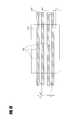
- FIG. 1Ais a cross-sectional view of a substrate having a plurality of mask lines formed thereon.
- FIG. 1Bis a cross-sectional view of the substrate of FIG. 1A after an anisotropic etch process transferring the mask pattern into a temporary layer.
- FIG. 1Cis a cross-sectional view of the substrate of FIG. 1B after removal of the mask lines and an isotropic “shrink” etch.
- FIG. 1Dis a cross-sectional view of the substrate of FIG. 1C after blanket deposition of a spacer material of mandrels left in the temporary layer.
- FIG. 1Eis a cross-sectional view of the substrate of FIG. 1D after a directional spacer etch process to leave pitch-multiplied features or spacers.
- FIG. 1Fis a cross-sectional view of the substrate of FIG. 1E after removal of the mandrels.
- FIG. 2is a schematic top view of an exemplary partially formed integrated circuit.
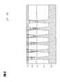
- FIG. 3is a schematic, cross-sectional side view of the partially formed integrated circuit of FIG. 2 after forming a plurality of pitch-multiplied features in and over the substrate.
- FIG. 4is a schematic, cross-sectional side view of the partially formed integrated circuit of FIG. 3 after forming an insulating film thereover.
- FIG. 5is a schematic, cross-sectional side view of the partially formed integrated circuit of FIG. 4 after forming a hard mask layer thereover.
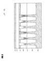
- FIG. 6Ais a schematic, cross-sectional side view of the partially formed integrated circuit of FIG. 5 after forming a plurality of spacers thereover.
- FIG. 6Bis a schematic top view of the partially formed integrated circuit of FIG. 6A .
- FIG. 7is a schematic, cross-sectional side view of the partially formed integrated circuit of FIG. 6A after deposition of a bottom antireflective coating (“BARC”) thereover.
- BARCbottom antireflective coating
- FIG. 8Ais a schematic, cross-sectional side view of the partially formed integrated circuit of FIG. 7 after formation of a second photoresist pattern thereover.
- FIG. 8Bis a schematic top view of the partially formed integrated circuit of FIG. 8A .
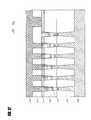
- FIG. 9is a schematic, cross-sectional side view of the partially formed integrated circuit of FIG. 8A after etching the bottom antireflective coating.
- FIG. 10Ais a schematic, view of the partially formed integrated circuit of FIG. 9 after etching the hard mask layer through the spacers and the second photoresist pattern; the view is a cross-section taken along a line perpendicular to a spacer loop.
- FIG. 10Bis a schematic view of the partially formed integrated circuit of FIG. 9 after etching the hard mask layer through the spacers and the second photoresist pattern; the view is a cross-section taken along the length of a spacer loop.
- FIG. 11is a schematic, cross-sectional view of the partially formed integrated circuit of FIG. 10A after etching insulating film and removing the photoresist, the BARC and the spacers.
- FIG. 12is a schematic, cross-sectional view of the partially formed integrated circuit of FIG. 11 after deposition of a conductive material thereover.
- FIG. 13is a schematic, cross-sectional view of the partially formed integrated circuit of FIG. 12 after a chemical mechanical planarization process is performed.
- FIG. 14is a flowchart illustrating an exemplary process for forming certain of the integrated circuit structures disclosed herein.
- FIG. 15is a schematic top view of a partially formed integrated circuit including spacer loops and a metal layer.
- FIG. 16is a schematic, cross-sectional view of the partially formed integrated circuit of FIG. 13 , further including an overhead contact between the array region and the peripheral region.
- FIG. 17Ais a layout view of a first mask formed by a photolithographic process; the first mask defines a plurality of mandrels.
- FIG. 17Bis a layout view of a spacer pattern obtained by performing a pitch multiplication technique on the mandrels of FIG. 17A .
- FIG. 17Cis a layout view of a partially formed integrated circuit formed by application of a second metal mask to the spacer pattern of FIG. 17B .
- Pitch doublingis one method proposed for extending the capabilities of photolithographic techniques beyond their minimum pitch. Such a method is illustrated in FIGS. 1A-1F and is described in U.S. Pat. No. 5,328,810 (issued 12 Jul. 1994), the entire disclosure of which is incorporated herein by reference.
- photolithographyis first used to form a pattern of lines 10 in a photoresist layer overlying a layer 20 of a temporary or expendable material and a substrate 30 .
- Common wavelengths which are used in performing the photolithographyinclude, but are not limited to, 157 nm, 193 nm, 248 nm or 365 nm. As shown in FIG.
- the patternis then transferred by an etch step, such as an anisotropic etch step, to the temporary layer 20 , thereby forming placeholders or mandrels 40 .
- the photoresist lines 10can be stripped and the mandrels 40 can be isotropically etched to increase the distance between neighboring mandrels 40 , as shown in FIG. 1C .
- a layer 50 of spacer materialis subsequently deposited over the mandrels 40 , as shown in FIG. 1D .
- Spacers 60are then formed on the sides of the mandrels 40 by preferentially etching the spacer material from the horizontal surfaces in a directional spacer etch, as shown in FIG. 1E .
- the remaining mandrels 40are then removed, leaving behind only the spacers 60 , which together act as a mask for patterning, as shown in FIG. 1F .
- spacers 60which together act as a mask for patterning, as shown in FIG. 1F .
- pitch multiplicationrefers to the process generally, regardless of the number of times the spacer formation process is employed.
- the layer 50 of spacer materialtypically has a single thickness 90 (see FIGS. 1D and 1E ), and because the sizes of the features formed by the spacers 60 usually corresponds to that thickness 90 , the pitch doubling technique typically produces features of only one width.
- integrated circuitsoften include features of different sizes.
- random access memory circuitstypically contain arrays of memory cells and logic circuits in the so-called “periphery”.
- the memory cellsare typically connected by conductive lines and, in the periphery, the conductive lines typically contact landing pads for connecting arrays to logic.
- Peripheral features such as landing padscan be larger than the conductive lines.
- peripheral electrical devicessuch as transistors are preferably larger than electrical devices in the array.
- the flexibility required to define circuitswill typically not be possible using a single mask, particularly if the patterns are limited to those that can be formed along the sidewalls of resist patterns.
- Some proposed methods for forming patterns at the periphery and at the arrayinvolve three separate masks. For example, in one method, a first mask and pitch doubling are used to form a spacer pattern, which typically comprises spacer loops in one region of a chip, such as the array region of a memory device. Then, a second mask is performed to form a second pattern in another region of the chip, such as the peripheral region of a memory device. This second peripheral pattern is formed in a layer overlying the spacer pattern. This covers the central portion of the spacer loops while the looped ends of the spacers are left exposed to an etching process. Then, a third mask is performed to form a third pattern that includes interconnects in and/or from the peripheral region.
- Both the “chopped” spacer pattern and the third patternare then transferred to an underlying masking layer which can be etched relative to an underlying substrate.
- Thisallows features having different sizes—as compared to each other and as compared to the spacer loops—to be formed in the circuit peripheral region.
- Such featuresinclude, for example, interconnect patterns. These features can overlap with the spacer loops, can be consolidated with features in the circuit array region, and can be subsequently etched.
- part of the feature pattern to be transferred to a substratehas a pitch below the minimum pitch of the photolithographic technique used for processing the substrate.
- certain embodimentscan be used to form devices having arrays of electrical devices, including logic or gate arrays and volatile and non-volatile memory devices such as DRAM, read only memory (“ROM”), flash memory and gate arrays.
- pitch multiplicationis usable to form, for example, transistor gate electrodes and conductive lines in the array region of the chips, while conventional photolithography is usable to form larger features, such as contacts, at the peripheries of the chips. Exemplary masking steps in the course of fabricating a memory device are illustrated in the figures and are described herein.
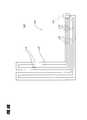
- FIG. 2shows a top view of an exemplary partially fabricated integrated circuit 100 , such as a memory chip.
- a central array region 102is surrounded by a peripheral region 104 .
- the array 102will typically by densely populated with conducting lines and electrical devices such as transistors and capacitors.
- Pitch multiplicationcan be used to form features in the array region 102 , as discussed herein.
- the peripheral region 104optionally includes features larger than those in the array region 102 .
- Conventional photolithography, rather than pitch multiplicationis typically used to pattern these larger features, examples of which include various types of logic circuitry. The geometric complexity of the logic circuits located in the peripheral region 104 makes using pitch multiplication difficult.
- peripheral region 104may require larger geometries due to electrical constraints, thereby making pitch multiplication less advantageous than conventional photolithography for such devices.
- the relative positions, and the number of peripheral regions 104 and array regions 102 in the integrated circuit 100can vary in other embodiments.
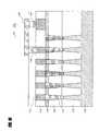
- FIG. 3shows a partial cross-sectional view of the partially fabricated integrated circuit of FIG. 2 , including portions of the array region 102 and the peripheral region 104 .
- a photolithography techniquea plurality of trenches are etched into a substrate 108 , and these trenches are filled with an insulator 105 , such as an oxide.
- the insulator 105is a field isolation layer, and in an exemplary embodiment is a shallow trench isolation (“STI”) layer deposited in a high density plasma (“HDP”), spin-on dielectric (“SOD”), flow-fill or TEOS process.
- HDPhigh density plasma
- SODspin-on dielectric
- flow-fill or TEOS processa high density plasma
- the SODis deposited and densified.
- An upper interlevel dielectric (“ILD”) insulator 106is formed over the substrate, and contact is made through the ILD 106 by etching contact holes and filling with conductive plugs 110 .
- the conductive plugs 110comprise polycrystalline silicon, although other electrically conductive materials can be used in other embodiments.
- Portions of an etch stop layer 112such as a nitride layer, are disposed over the insulator 106 ; the etch stop layer 112 is used in the formation of the conductive plugs 110 .
- the insulator 105is aligned with the substrate/plug interface. However, in other embodiments the insulator 105 extends slightly above the substrate/plug interface, as illustrated in FIG. 3 .
- the feature size in the array region 102is smaller than the feature size in the peripheral region 104 .
- the conductive plugs 110have a feature size of approximately 50 nm. In a preferred embodiment, the conductive plugs 110 have a feature size between approximately 30 nm and approximately 100 nm. More preferably, the conductive plugs have a feature size between approximately 32.5 nm and approximately 65 nm. Other feature sizes for the conductive plugs 110 can be used in other embodiments. Additional details regarding the techniques used to form the conductive plugs are provided in U.S. patent application Ser. No. 11/215982 (filed concurrently herewith).
- an insulator film 114 in which damascene trenches are to be formedis deposited over the film stack illustrated in FIG. 3 .
- the insulator filmcomprises an un-doped oxide film, such as an oxide film deposited from tetra ethyl ortho-silicate (“TEOS”), while in other embodiments the insulator film comprises a doped oxide film, such as BPSG or PSG. Other non-oxide insulators can be used in still other embodiments.
- the insulator film 114is deposited to a thickness corresponding to the conductor height to be formed in the integrated circuit.
- a hard mask layer 116is deposited over the insulator film 114 .
- the hard mask layer 116comprises amorphous silicon, although other materials can be used in other embodiments.
- a plurality of spacers 118are formed over the hard mask layer 116 .
- the spacersare formed using a pitch doubling technique such as that illustrated in FIGS. 1A through 1F , using the disclosed photoresist mask, transfer to a temporary layer, isotropic etch and spacer process.
- the spacerscomprise a low temperature oxide material that can be etched selectively with respect to the underlying hard mask layer 116 .
- the spacersare deposited at a temperature less than about 400° C.
- the spacersare deposited using an atomic layer deposition process. Exemplary materials for the spacers include silicon oxide, silicon nitride, polycrystalline silicon and carbon.
- gaps 120that correspond to regions of the integrated circuit where conductive material is to be deposited.
- the gaps 120are vertically aligned with the conductive plugs 110 .
- the spacing between the spacers 118 and the gaps 120varies between the array region 102 and the peripheral region 104 of the integrated circuit 100 .
- FIG. 6Bschematically shows a top view of the spacers 118 and the intervening gaps 120 .
- FIG. 6Balso illustrates that the spacers 118 generally follow the outline of the lines formed in the photo definable layer, thereby forming a plurality of looped ends 124 .
- a BARC 122is applied over the spacers 118 .
- the BARC 122is optionally applied in a spin-on process, thereby providing a substantially planar surface.
- a second maskis applied.
- the second maskresults in a pattern of photoresist 126 being deposited over the integrated circuit.
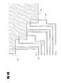
- the photoresist patterndefines a blocked region that blocks the looped ends 124 of the spacers 118 and defines one or more openings 128 in the peripheral region 104 . This is illustrated in FIGS. 8A (side view) and 8 B (top view). As illustrated in FIG.
- the second maskis spaced apart from the spacers 118 by a gap 120 a , and is spaced apart from the spacer looped ends 124 by a gap 120 b .
- the gaps 120 a , 120 baccommodate misalignment of the second mask with respect to the spacer pattern.
- the minimum width of the openings 128depends on the native resolution of the photolithographic process, which in one embodiment is as low as 100 nm, which in another embodiment is as low as 65 nm, and which in another embodiment is as low as 45 nm. Other dimensions can be used in other embodiments.
- the spacers 118 in the circuit array region 104are sufficiently spaced apart to allow contacts 132 to be “landed” to provide interconnections to other levels of the integrated circuit.
- the BARC 122is etched, as illustrated in FIG. 9 .
- the pattern defined by the second mask, including the blocked regionis transferred to an intermediate layer before etching the BARC.
- intermediate layer or the BARC aloneis used to block the looped ends 124 of the spacers 118 .
- the BARC etchis followed by an etch of the hard mask layer 116 , which can be selectively etched with respect to the spacers 118 .
- the resulting structureis illustrated in FIG. 10A (which is a cross-sectional view taken along a line perpendicular to a spacer loop) and in FIG. 10B (which is a cross-sectional view taken along the length of a spacer loop).
- the hard mask etchis a dry etch process. This is followed by successive removal of the photoresist 126 and BARC 122 , followed by an oxide etch. In such embodiments, the oxide etch will remove both the spacers 118 and exposed portions of the insulator film 114 .
- the conductive plugs 110provide an etch stop.
- the resulting structurewhich is illustrated in FIG. 11 , includes a pattern of trenches exposing the conductive plugs 110 in the array region 102 , and a pattern of other openings 128 in the hard mask layer 116 in the peripheral region 104 .
- This sequenceadvantageously lowers the effective aspect ratio for the trenches.
- the insulator film 114 illustrated in FIGS. 10A and 10Bis etched without prior removal of the spacers 118 .
- the BARC 122is optionally omitted in embodiments wherein the substrate material is not reflective.
- the etch processes illustrated in FIGS. 10A , 10 B and 11advantageously consolidate two mask patterns: the pattern formed by the spacers 118 in the array region 102 , and the pattern formed by the photoresist 126 in the peripheral region. This effectively forms a superposition of two distinct patterns, which allows etching through the gaps 120 between the spacers 118 in regions of the integrated circuit 100 not covered by the second photoresist layer 126 .
- conductive material 130is then deposited over the partially formed integrated circuit.
- the hard mask layer 116is removed before deposition of the conductive material 130 .
- Suitable conductive materialsinclude, but are not limited to, titanium, titanium nitride, tungsten, tantalum nitride and copper.
- the conductive material 130is deposited to a thickness sufficient such that the widest trench width in the periphery is filled.
- CMPchemical mechanical planarization
- FIG. 14A flowchart illustrating an exemplary process for forming certain of the integrated circuit structures disclosed herein is provided in FIG. 14 .
- a plurality of featuresare defined in a first resist layer in an array region of the memory device in an operational block 150 .
- resist layersthat can be used to define the features are photoresist layers and imprinted resist layers.
- pitch multiplicationis used to define a plurality of spacer loops in a lower masking layer in an operational block 152 .
- the spacer loopsare formed over the patterned resist features, although this is less preferred because resist is generally unable to withstand spacer deposition and etch processes.
- the ends of the spacer loopsare blocked with a second resist layer that also defines features in a periphery region of the integrated circuit in an operational block 156 .
- a second resist layerthat also defines features in a periphery region of the integrated circuit in an operational block 156 .
- an insulating layer in the gaps between the spacersis etched, the etching being performed in a pattern defined by the second resist layer in an operational block 158 .
- a metal fill and subsequent CMP processcan then be performed over the partially-formed integrated circuit in an operational block 160 , thereby allowing metal lines to be formed in the integrated circuit array region (operational block 162 ) and electrical interconnects to be formed in the integrated circuit peripheral region (operational block 164 ).
- the interconnectsare optionally used to connect integrated circuit components, such as logic components, within the periphery.
- the second maskcan define other patterns, such as capacitors, contacts, resistors, simultaneously with blocking the spacer loops.
- the peripheral interconnectsare also optionally used to form electrical connections between the array region 102 and the peripheral region 104 . This is illustrated in operational block 166 of FIG. 14 .
- such contactscan be formed in a plane above the damascene structure illustrated in FIG. 13 .
- An example of such an “overhead” contactis provided in FIG. 16 .
- the overhead contactincludes a plurality of contacts 146 connected by an interconnect line 148 .
- FIG. 17A through 17Cprovide a top-down view of an exemplary embodiment of the methods illustrated in FIG. 14 .
- FIG. 17Aillustrates a first mask 134 defined by a photolithographic process.
- the first mask 134is defined in a layer of photoresist material, although in other embodiments the first mask 134 is transferred to another layer, such as an amorphous carbon layer.
- FIG. 17Billustrates a spacer pattern 136 created by first shrinking the first mask 134 using an isotropic etch process, and then performing a pitch doubling technique on the shrunken first mask.
- Application of a second metal mask 138yields the exemplary structure illustrated in FIG. 17C .
- This structureincludes widened portions in the spacer pattern configured to receive contacts 139 from other layers of the integrated circuit.
- Certain of the integrated circuit fabrication techniques disclosed hereinoffer significant advantages over conventional techniques. For example, conventional methodology requires three separate masks to define the array region, to define the peripheral region, and to remove the looped ends of circuit features. In contrast, certain of the techniques disclosed herein allow pitch reduced features to be formed in a damascene process that uses only two masks. As described herein, in exemplary embodiments the looped ends of array features can be blocked with the same mask that is used to define periphery features.
- rulesare provided to facilitate circuit designers to implement the integrated circuit fabrication methods disclosed herein.
- the configuration of the masksindirectly corresponds to the integrated circuit patterns that are formed, particularly when the gaps between the spacer loops, some of which are enclosed and some of which are not, define the circuit features of interest.
- Such featurescan be formed as disclosed herein using pitch multiplication and damascene techniques.
- the rules discussed belowprovide a circuit designer with guidelines for building a circuit that is formable using the techniques disclosed herein. As described herein, building a circuit is compliance with these rules allows mixed use of interconnects with varying pitch size while using only two masks.
- spacer layer maskis used to define pitch-reduced spacers between dense interconnect lines in the circuit array region
- metalis used to define the interconnect pattern in the circuit periphery region.
- the design rules for defining the spacer and metalare based on two scaling factors.
- Fis the minimum feature size that can be resolved
- Dis the maximum misalignment allowed between the two masks.
- the variable xis a pitch multiplication scaling constant corresponding to a feature size of the spacer loops used to define the metal lines (0 ⁇ x ⁇ 1). Because a single pitch-multiplication technique is used, the actual interconnect pitch achievable using the techniques disclosed herein is F.
- the spacer loopsare drawn in a plurality of distinct closed loops that to not overlap or cross.
- Two exemplary spacer loops 140are illustrated in FIG. 15 , which is a top view of an exemplary in-process integrated circuit simplified for illustration. As illustrated, the spacer loops have a minimum width of xF, and have a minimum space of (1 ⁇ x)F.
- a plurality of metal features 144are defined by a plurality of spacer loops 140 . Because a damascene process is used in the preferred embodiments, the gaps between the spacer loops, some of which are enclosed and some of which are not, define the metal features 144 that will subsequently be deposited (for example, by physical vapor deposition or chemical vapor deposition) or electroplated with conductive material.
- metal features 142are defined only one side by the spacer loops 140 .
- the metal features 144 that are defined on both sides by the spacer loops 140have a minimum width of (1 ⁇ x)F.
- the metal features 142 that are defined on only one side by a spacer loop 140have a minimum width of ((1 ⁇ x)F+D).
- Metal featurescan also be formed without restriction by a spacer loop 140 with a minimum width corresponding to the minimum resolution of the lithography technique F.
- the metal features 144have a minimum spacing of xF if separated by a spacer loop 140
- the metal features 142have a minimum spacing of F if separated by empty space or by a spacer loop 140 on only one side. If a metal feature 142 or 144 is present on both sides of a spacer loop 140 , then the metal is drawn in contact with (that is, the metal occupies directly adjacent real estate with) the spacer loop 140 . If the metal feature 142 is present on only one side of the spacer loop 140 , then a minimum space of min(D ⁇ xF, 0) separates the metal feature 144 from the spacer loop 140 .
- circuit design rules expounded hereinare based on the integrated circuit fabrication techniques disclosed herein.
- using an oversized spacer mask to define subsequently pitch-reduced featureslimits the spacing of metal lines that are defined by the pitch-reduced features.
- Certain embodiments disclosed hereinare usable to form a wide variety of integrated circuits.
- integrated circuitsinclude, but are not limited to, circuits having arrays of electrical devices, such as memory cell arrays for volatile and non-volatile memory devices such as DRAM, ROM or flash memory, NAND flash memory, and integrated circuits having logic or gate arrays.
- the logic arraycan be a field programmable gate array (“FPGA”) having a core array similar to a memory array and a periphery with supporting logic circuitry. Therefore, the integrated circuit formed using the techniques disclosed herein can be, for example, a memory chip or a processor, which can include both a logic array and embedded memory, or other integrated circuits having a logic or gate array.
Landscapes
- Engineering & Computer Science (AREA)
- Microelectronics & Electronic Packaging (AREA)
- Condensed Matter Physics & Semiconductors (AREA)
- General Physics & Mathematics (AREA)
- Computer Hardware Design (AREA)
- Physics & Mathematics (AREA)
- Power Engineering (AREA)
- Manufacturing & Machinery (AREA)
- Chemical & Material Sciences (AREA)
- Inorganic Chemistry (AREA)
- Chemical Kinetics & Catalysis (AREA)
- General Chemical & Material Sciences (AREA)
- Internal Circuitry In Semiconductor Integrated Circuit Devices (AREA)
- Semiconductor Memories (AREA)
- Exposure Of Semiconductors, Excluding Electron Or Ion Beam Exposure (AREA)
Abstract
Description
Claims (19)
Priority Applications (4)
| Application Number | Priority Date | Filing Date | Title |
|---|---|---|---|
| US13/445,797US8507341B2 (en) | 2005-03-28 | 2012-04-12 | Integrated circuit fabrication |
| US13/962,208US8859362B2 (en) | 2005-03-28 | 2013-08-08 | Integrated circuit fabrication |
| US14/486,890US9147608B2 (en) | 2005-03-28 | 2014-09-15 | Integrated circuit fabrication |
| US14/855,845US9412594B2 (en) | 2005-03-28 | 2015-09-16 | Integrated circuit fabrication |
Applications Claiming Priority (5)
| Application Number | Priority Date | Filing Date | Title |
|---|---|---|---|
| US66603105P | 2005-03-28 | 2005-03-28 | |
| US11/216,477US7611944B2 (en) | 2005-03-28 | 2005-08-31 | Integrated circuit fabrication |
| US12/119,831US7776683B2 (en) | 2005-03-28 | 2008-05-13 | Integrated circuit fabrication |
| US12/850,511US8158476B2 (en) | 2005-03-28 | 2010-08-04 | Integrated circuit fabrication |
| US13/445,797US8507341B2 (en) | 2005-03-28 | 2012-04-12 | Integrated circuit fabrication |
Related Parent Applications (1)
| Application Number | Title | Priority Date | Filing Date |
|---|---|---|---|
| US12/850,511DivisionUS8158476B2 (en) | 2005-03-28 | 2010-08-04 | Integrated circuit fabrication |
Related Child Applications (1)
| Application Number | Title | Priority Date | Filing Date |
|---|---|---|---|
| US13/962,208ContinuationUS8859362B2 (en) | 2005-03-28 | 2013-08-08 | Integrated circuit fabrication |
Publications (2)
| Publication Number | Publication Date |
|---|---|
| US20120193777A1 US20120193777A1 (en) | 2012-08-02 |
| US8507341B2true US8507341B2 (en) | 2013-08-13 |
Family
ID=36617080
Family Applications (8)
| Application Number | Title | Priority Date | Filing Date |
|---|---|---|---|
| US11/216,477Active2028-09-03US7611944B2 (en) | 2005-03-28 | 2005-08-31 | Integrated circuit fabrication |
| US11/407,429Active2027-08-24US7648919B2 (en) | 2005-03-28 | 2006-04-20 | Integrated circuit fabrication |
| US12/119,831Active2026-05-27US7776683B2 (en) | 2005-03-28 | 2008-05-13 | Integrated circuit fabrication |
| US12/850,511Active2025-11-10US8158476B2 (en) | 2005-03-28 | 2010-08-04 | Integrated circuit fabrication |
| US13/445,797Expired - LifetimeUS8507341B2 (en) | 2005-03-28 | 2012-04-12 | Integrated circuit fabrication |
| US13/962,208Expired - LifetimeUS8859362B2 (en) | 2005-03-28 | 2013-08-08 | Integrated circuit fabrication |
| US14/486,890Expired - LifetimeUS9147608B2 (en) | 2005-03-28 | 2014-09-15 | Integrated circuit fabrication |
| US14/855,845Expired - LifetimeUS9412594B2 (en) | 2005-03-28 | 2015-09-16 | Integrated circuit fabrication |
Family Applications Before (4)
| Application Number | Title | Priority Date | Filing Date |
|---|---|---|---|
| US11/216,477Active2028-09-03US7611944B2 (en) | 2005-03-28 | 2005-08-31 | Integrated circuit fabrication |
| US11/407,429Active2027-08-24US7648919B2 (en) | 2005-03-28 | 2006-04-20 | Integrated circuit fabrication |
| US12/119,831Active2026-05-27US7776683B2 (en) | 2005-03-28 | 2008-05-13 | Integrated circuit fabrication |
| US12/850,511Active2025-11-10US8158476B2 (en) | 2005-03-28 | 2010-08-04 | Integrated circuit fabrication |
Family Applications After (3)
| Application Number | Title | Priority Date | Filing Date |
|---|---|---|---|
| US13/962,208Expired - LifetimeUS8859362B2 (en) | 2005-03-28 | 2013-08-08 | Integrated circuit fabrication |
| US14/486,890Expired - LifetimeUS9147608B2 (en) | 2005-03-28 | 2014-09-15 | Integrated circuit fabrication |
| US14/855,845Expired - LifetimeUS9412594B2 (en) | 2005-03-28 | 2015-09-16 | Integrated circuit fabrication |
Country Status (5)
| Country | Link |
|---|---|
| US (8) | US7611944B2 (en) |
| EP (1) | EP1864320B1 (en) |
| JP (1) | JP5311116B2 (en) |
| KR (1) | KR100942862B1 (en) |
| WO (1) | WO2006104634A2 (en) |
Cited By (5)
| Publication number | Priority date | Publication date | Assignee | Title |
|---|---|---|---|---|
| US20130320552A1 (en)* | 2005-03-28 | 2013-12-05 | Micron Technology, Inc. | Integrated circuit fabrication |
| US20150170905A1 (en)* | 2007-07-30 | 2015-06-18 | Micron Technology, Inc. | Methods for device fabrication using pitch reduction and related devices |
| US20150364534A1 (en)* | 2014-06-17 | 2015-12-17 | International Business Machines Corporation | Non-planar capacitors with finely tuned capacitance values and methods of forming the non-planar capacitors |
| US9330913B2 (en) | 2010-06-28 | 2016-05-03 | Samsung Electronics Co., Ltd. | Semiconductor device and method of fabricating the same |
| US9728548B2 (en) | 2015-11-16 | 2017-08-08 | Micron Technology, Inc. | Vertical memory blocks and related devices and methods |
Families Citing this family (169)
| Publication number | Priority date | Publication date | Assignee | Title |
|---|---|---|---|---|
| US7151040B2 (en)* | 2004-08-31 | 2006-12-19 | Micron Technology, Inc. | Methods for increasing photo alignment margins |
| US7910288B2 (en)* | 2004-09-01 | 2011-03-22 | Micron Technology, Inc. | Mask material conversion |
| US7547945B2 (en)* | 2004-09-01 | 2009-06-16 | Micron Technology, Inc. | Transistor devices, transistor structures and semiconductor constructions |
| US7655387B2 (en)* | 2004-09-02 | 2010-02-02 | Micron Technology, Inc. | Method to align mask patterns |
| US7115525B2 (en)* | 2004-09-02 | 2006-10-03 | Micron Technology, Inc. | Method for integrated circuit fabrication using pitch multiplication |
| US7390746B2 (en) | 2005-03-15 | 2008-06-24 | Micron Technology, Inc. | Multiple deposition for integration of spacers in pitch multiplication process |
| US7253118B2 (en) | 2005-03-15 | 2007-08-07 | Micron Technology, Inc. | Pitch reduced patterns relative to photolithography features |
| US7384849B2 (en) | 2005-03-25 | 2008-06-10 | Micron Technology, Inc. | Methods of forming recessed access devices associated with semiconductor constructions |
| US7429536B2 (en) | 2005-05-23 | 2008-09-30 | Micron Technology, Inc. | Methods for forming arrays of small, closely spaced features |
| US7560390B2 (en) | 2005-06-02 | 2009-07-14 | Micron Technology, Inc. | Multiple spacer steps for pitch multiplication |
| US7396781B2 (en) | 2005-06-09 | 2008-07-08 | Micron Technology, Inc. | Method and apparatus for adjusting feature size and position |
| JP2006351861A (en) | 2005-06-16 | 2006-12-28 | Toshiba Corp | Manufacturing method of semiconductor device |
| US7888721B2 (en) | 2005-07-06 | 2011-02-15 | Micron Technology, Inc. | Surround gate access transistors with grown ultra-thin bodies |
| US7282401B2 (en) | 2005-07-08 | 2007-10-16 | Micron Technology, Inc. | Method and apparatus for a self-aligned recessed access device (RAD) transistor gate |
| US7786512B2 (en) | 2005-07-18 | 2010-08-31 | Saifun Semiconductors Ltd. | Dense non-volatile memory array and method of fabrication |
| US7768051B2 (en) | 2005-07-25 | 2010-08-03 | Micron Technology, Inc. | DRAM including a vertical surround gate transistor |
| US7413981B2 (en) | 2005-07-29 | 2008-08-19 | Micron Technology, Inc. | Pitch doubled circuit layout |
| US8123968B2 (en) | 2005-08-25 | 2012-02-28 | Round Rock Research, Llc | Multiple deposition for integration of spacers in pitch multiplication process |
| US7867851B2 (en) | 2005-08-30 | 2011-01-11 | Micron Technology, Inc. | Methods of forming field effect transistors on substrates |
| US7816262B2 (en) | 2005-08-30 | 2010-10-19 | Micron Technology, Inc. | Method and algorithm for random half pitched interconnect layout with constant spacing |
| US7829262B2 (en) | 2005-08-31 | 2010-11-09 | Micron Technology, Inc. | Method of forming pitch multipled contacts |
| US7696567B2 (en) | 2005-08-31 | 2010-04-13 | Micron Technology, Inc | Semiconductor memory device |
| US7557032B2 (en) | 2005-09-01 | 2009-07-07 | Micron Technology, Inc. | Silicided recessed silicon |
| US7393789B2 (en)* | 2005-09-01 | 2008-07-01 | Micron Technology, Inc. | Protective coating for planarization |
| US7572572B2 (en) | 2005-09-01 | 2009-08-11 | Micron Technology, Inc. | Methods for forming arrays of small, closely spaced features |
| US7416943B2 (en) | 2005-09-01 | 2008-08-26 | Micron Technology, Inc. | Peripheral gate stacks and recessed array gates |
| US7776744B2 (en) | 2005-09-01 | 2010-08-17 | Micron Technology, Inc. | Pitch multiplication spacers and methods of forming the same |
| US7687342B2 (en) | 2005-09-01 | 2010-03-30 | Micron Technology, Inc. | Method of manufacturing a memory device |
| US7759197B2 (en)* | 2005-09-01 | 2010-07-20 | Micron Technology, Inc. | Method of forming isolated features using pitch multiplication |
| KR100677998B1 (en)* | 2005-09-30 | 2007-02-02 | 동부일렉트로닉스 주식회사 | Shallow Trench Isolation Method for Semiconductor Devices |
| US20070120180A1 (en)* | 2005-11-25 | 2007-05-31 | Boaz Eitan | Transition areas for dense memory arrays |
| JP4865324B2 (en)* | 2005-12-26 | 2012-02-01 | キヤノン株式会社 | Information processing apparatus and information processing apparatus control method |
| EP1804282A1 (en)* | 2005-12-29 | 2007-07-04 | Interuniversitair Microelektronica Centrum vzw ( IMEC) | Methods for manufacturing dense integrated circuits |
| US7700441B2 (en) | 2006-02-02 | 2010-04-20 | Micron Technology, Inc. | Methods of forming field effect transistors, methods of forming field effect transistor gates, methods of forming integrated circuitry comprising a transistor gate array and circuitry peripheral to the gate array, and methods of forming integrated circuitry comprising a transistor gate array including first gates and second grounded isolation gates |
| US7638835B2 (en) | 2006-02-28 | 2009-12-29 | Saifun Semiconductors Ltd. | Double density NROM with nitride strips (DDNS) |
| US7476933B2 (en) | 2006-03-02 | 2009-01-13 | Micron Technology, Inc. | Vertical gated access transistor |
| US7842558B2 (en) | 2006-03-02 | 2010-11-30 | Micron Technology, Inc. | Masking process for simultaneously patterning separate regions |
| US7579278B2 (en)* | 2006-03-23 | 2009-08-25 | Micron Technology, Inc. | Topography directed patterning |
| US7902074B2 (en) | 2006-04-07 | 2011-03-08 | Micron Technology, Inc. | Simplified pitch doubling process flow |
| US8003310B2 (en)* | 2006-04-24 | 2011-08-23 | Micron Technology, Inc. | Masking techniques and templates for dense semiconductor fabrication |
| US7488685B2 (en) | 2006-04-25 | 2009-02-10 | Micron Technology, Inc. | Process for improving critical dimension uniformity of integrated circuit arrays |
| US7795149B2 (en) | 2006-06-01 | 2010-09-14 | Micron Technology, Inc. | Masking techniques and contact imprint reticles for dense semiconductor fabrication |
| US7723009B2 (en)* | 2006-06-02 | 2010-05-25 | Micron Technology, Inc. | Topography based patterning |
| US8852851B2 (en)* | 2006-07-10 | 2014-10-07 | Micron Technology, Inc. | Pitch reduction technology using alternating spacer depositions during the formation of a semiconductor device and systems including same |
| US7602001B2 (en)* | 2006-07-17 | 2009-10-13 | Micron Technology, Inc. | Capacitorless one transistor DRAM cell, integrated circuitry comprising an array of capacitorless one transistor DRAM cells, and method of forming lines of capacitorless one transistor DRAM cells |
| KR100823706B1 (en) | 2006-07-21 | 2008-04-21 | 삼성전자주식회사 | Signal line structure of a semiconductor device and method of manufacturing the same |
| US7772632B2 (en) | 2006-08-21 | 2010-08-10 | Micron Technology, Inc. | Memory arrays and methods of fabricating memory arrays |
| US7611980B2 (en) | 2006-08-30 | 2009-11-03 | Micron Technology, Inc. | Single spacer process for multiplying pitch by a factor greater than two and related intermediate IC structures |
| JP5111980B2 (en) | 2006-09-06 | 2013-01-09 | 株式会社東芝 | Semiconductor device |
| US7589995B2 (en) | 2006-09-07 | 2009-09-15 | Micron Technology, Inc. | One-transistor memory cell with bias gate |
| US7666578B2 (en) | 2006-09-14 | 2010-02-23 | Micron Technology, Inc. | Efficient pitch multiplication process |
| US8129289B2 (en) | 2006-10-05 | 2012-03-06 | Micron Technology, Inc. | Method to deposit conformal low temperature SiO2 |
| US7790360B2 (en)* | 2007-03-05 | 2010-09-07 | Micron Technology, Inc. | Methods of forming multiple lines |
| US7709390B2 (en)* | 2007-05-31 | 2010-05-04 | Micron Technology, Inc. | Methods of isolating array features during pitch doubling processes and semiconductor device structures having isolated array features |
| US7807578B2 (en)* | 2007-06-01 | 2010-10-05 | Applied Materials, Inc. | Frequency doubling using spacer mask |
| US7923373B2 (en) | 2007-06-04 | 2011-04-12 | Micron Technology, Inc. | Pitch multiplication using self-assembling materials |
| KR101393306B1 (en) | 2007-07-13 | 2014-05-09 | 삼성전자주식회사 | Register having a security function and computer system thereof |
| US8563229B2 (en)* | 2007-07-31 | 2013-10-22 | Micron Technology, Inc. | Process of semiconductor fabrication with mask overlay on pitch multiplied features and associated structures |
| US8481417B2 (en) | 2007-08-03 | 2013-07-09 | Micron Technology, Inc. | Semiconductor structures including tight pitch contacts and methods to form same |
| US8021933B2 (en)* | 2007-08-29 | 2011-09-20 | Qimonda Ag | Integrated circuit including structures arranged at different densities and method of forming the same |
| US7737039B2 (en)* | 2007-11-01 | 2010-06-15 | Micron Technology, Inc. | Spacer process for on pitch contacts and related structures |
| US7659208B2 (en) | 2007-12-06 | 2010-02-09 | Micron Technology, Inc | Method for forming high density patterns |
| US7790531B2 (en) | 2007-12-18 | 2010-09-07 | Micron Technology, Inc. | Methods for isolating portions of a loop of pitch-multiplied material and related structures |
| KR100919349B1 (en)* | 2007-12-27 | 2009-09-25 | 주식회사 하이닉스반도체 | Metal wiring formation method of semiconductor device |
| US8030218B2 (en) | 2008-03-21 | 2011-10-04 | Micron Technology, Inc. | Method for selectively modifying spacing between pitch multiplied structures |
| JP2009295785A (en)* | 2008-06-05 | 2009-12-17 | Toshiba Corp | Method of manufacturing semiconductor device |
| US8404600B2 (en) | 2008-06-17 | 2013-03-26 | Micron Technology, Inc. | Method for forming fine pitch structures |
| US8076208B2 (en) | 2008-07-03 | 2011-12-13 | Micron Technology, Inc. | Method for forming transistor with high breakdown voltage using pitch multiplication technique |
| JP4789158B2 (en)* | 2008-08-18 | 2011-10-12 | 株式会社東芝 | Semiconductor device manufacturing method and semiconductor device |
| US8101497B2 (en) | 2008-09-11 | 2012-01-24 | Micron Technology, Inc. | Self-aligned trench formation |
| US7709396B2 (en)* | 2008-09-19 | 2010-05-04 | Applied Materials, Inc. | Integral patterning of large features along with array using spacer mask patterning process flow |
| US8492282B2 (en) | 2008-11-24 | 2013-07-23 | Micron Technology, Inc. | Methods of forming a masking pattern for integrated circuits |
| JP5322668B2 (en)* | 2009-01-21 | 2013-10-23 | 株式会社東芝 | Semiconductor device manufacturing method and photomask |
| US8680650B2 (en) | 2009-02-03 | 2014-03-25 | Micron Technology, Inc. | Capacitor structures having improved area efficiency |
| JP4901898B2 (en)* | 2009-03-30 | 2012-03-21 | 株式会社東芝 | Manufacturing method of semiconductor device |
| KR101616044B1 (en)* | 2009-07-03 | 2016-04-28 | 삼성전자주식회사 | Semiconductor device comprising landing pad formed by electroless plating |
| JP2011061003A (en)* | 2009-09-10 | 2011-03-24 | Elpida Memory Inc | Method of forming wiring pattern, method of forming semiconductor device, semiconductor device, and data processing system |
| US8003482B2 (en) | 2009-11-19 | 2011-08-23 | Micron Technology, Inc. | Methods of processing semiconductor substrates in forming scribe line alignment marks |
| US9324576B2 (en) | 2010-05-27 | 2016-04-26 | Applied Materials, Inc. | Selective etch for silicon films |
| FR2960657B1 (en)* | 2010-06-01 | 2013-02-22 | Commissariat Energie Atomique | LOW-DEPENDENT LITHOGRAPHY METHOD |
| KR20120053799A (en)* | 2010-11-18 | 2012-05-29 | 삼성전자주식회사 | A semiconductor device and a method of forming the same |
| WO2011015675A2 (en) | 2010-11-24 | 2011-02-10 | Phonak Ag | Hearing assistance system and method |
| US8741778B2 (en) | 2010-12-14 | 2014-06-03 | Applied Materials, Inc. | Uniform dry etch in two stages |
| US8420947B2 (en)* | 2010-12-30 | 2013-04-16 | Globalfoundries Singapore Pte. Ltd. | Integrated circuit system with ultra-low k dielectric and method of manufacture thereof |
| US8771539B2 (en) | 2011-02-22 | 2014-07-08 | Applied Materials, Inc. | Remotely-excited fluorine and water vapor etch |
| US8999856B2 (en) | 2011-03-14 | 2015-04-07 | Applied Materials, Inc. | Methods for etch of sin films |
| US9064815B2 (en) | 2011-03-14 | 2015-06-23 | Applied Materials, Inc. | Methods for etch of metal and metal-oxide films |
| WO2012130297A1 (en) | 2011-03-30 | 2012-10-04 | Phonak Ag | Wireless sound transmission system and method |
| US20140176297A1 (en) | 2011-05-04 | 2014-06-26 | Phonak Ag | Self-learning hearing assistance system and method of operating the same |
| US20120280354A1 (en)* | 2011-05-05 | 2012-11-08 | Synopsys, Inc. | Methods for fabricating high-density integrated circuit devices |
| US8765598B2 (en) | 2011-06-02 | 2014-07-01 | Micron Technology, Inc. | Conductive structures, systems and devices including conductive structures and related methods |
| US8771536B2 (en) | 2011-08-01 | 2014-07-08 | Applied Materials, Inc. | Dry-etch for silicon-and-carbon-containing films |
| US8679982B2 (en) | 2011-08-26 | 2014-03-25 | Applied Materials, Inc. | Selective suppression of dry-etch rate of materials containing both silicon and oxygen |
| EP2701181A2 (en) | 2011-08-26 | 2014-02-26 | Espros Photonics AG | Method for producing semiconductor components on a substrate and substrate with semiconductor components |
| US8679983B2 (en) | 2011-09-01 | 2014-03-25 | Applied Materials, Inc. | Selective suppression of dry-etch rate of materials containing both silicon and nitrogen |
| US8927390B2 (en) | 2011-09-26 | 2015-01-06 | Applied Materials, Inc. | Intrench profile |
| US8808563B2 (en) | 2011-10-07 | 2014-08-19 | Applied Materials, Inc. | Selective etch of silicon by way of metastable hydrogen termination |
| WO2013070436A1 (en) | 2011-11-08 | 2013-05-16 | Applied Materials, Inc. | Methods of reducing substrate dislocation during gapfill processing |
| DK2805464T3 (en) | 2012-01-20 | 2016-07-04 | Sonova Ag | Wireless audio transmission and method |
| US8741776B2 (en)* | 2012-02-07 | 2014-06-03 | Taiwan Semiconductor Manufacturing Company, Ltd. | Patterning process for fin-like field effect transistor (finFET) device |
| US9102121B2 (en)* | 2012-05-03 | 2015-08-11 | Micron Technology, Inc. | Substrates and methods of forming a pattern on a substrate |
| US8637406B1 (en) | 2012-07-19 | 2014-01-28 | International Business Machines Corporation | Image transfer process employing a hard mask layer |
| US8969213B2 (en) | 2012-07-30 | 2015-03-03 | International Business Machines Corporation | Non-lithographic line pattern formation |
| US9373517B2 (en) | 2012-08-02 | 2016-06-21 | Applied Materials, Inc. | Semiconductor processing with DC assisted RF power for improved control |
| US9034770B2 (en) | 2012-09-17 | 2015-05-19 | Applied Materials, Inc. | Differential silicon oxide etch |
| US9023734B2 (en) | 2012-09-18 | 2015-05-05 | Applied Materials, Inc. | Radical-component oxide etch |
| US9390937B2 (en) | 2012-09-20 | 2016-07-12 | Applied Materials, Inc. | Silicon-carbon-nitride selective etch |
| US9132436B2 (en) | 2012-09-21 | 2015-09-15 | Applied Materials, Inc. | Chemical control features in wafer process equipment |
| US8765574B2 (en) | 2012-11-09 | 2014-07-01 | Applied Materials, Inc. | Dry etch process |
| US8969212B2 (en) | 2012-11-20 | 2015-03-03 | Applied Materials, Inc. | Dry-etch selectivity |
| US8980763B2 (en) | 2012-11-30 | 2015-03-17 | Applied Materials, Inc. | Dry-etch for selective tungsten removal |
| US9064816B2 (en) | 2012-11-30 | 2015-06-23 | Applied Materials, Inc. | Dry-etch for selective oxidation removal |
| US9111877B2 (en) | 2012-12-18 | 2015-08-18 | Applied Materials, Inc. | Non-local plasma oxide etch |
| US8921234B2 (en) | 2012-12-21 | 2014-12-30 | Applied Materials, Inc. | Selective titanium nitride etching |
| US10256079B2 (en) | 2013-02-08 | 2019-04-09 | Applied Materials, Inc. | Semiconductor processing systems having multiple plasma configurations |
| TWI487004B (en)* | 2013-03-01 | 2015-06-01 | Winbond Electronics Corp | Patterning method and method of forming memory device |
| US9362130B2 (en) | 2013-03-01 | 2016-06-07 | Applied Materials, Inc. | Enhanced etching processes using remote plasma sources |
| US9040422B2 (en) | 2013-03-05 | 2015-05-26 | Applied Materials, Inc. | Selective titanium nitride removal |
| KR102059183B1 (en) | 2013-03-07 | 2019-12-24 | 삼성전자주식회사 | Method of forming semiconductor device and the device |
| US8801952B1 (en) | 2013-03-07 | 2014-08-12 | Applied Materials, Inc. | Conformal oxide dry etch |
| US10170282B2 (en) | 2013-03-08 | 2019-01-01 | Applied Materials, Inc. | Insulated semiconductor faceplate designs |
| US20140271097A1 (en) | 2013-03-15 | 2014-09-18 | Applied Materials, Inc. | Processing systems and methods for halide scavenging |
| JP2014183135A (en)* | 2013-03-18 | 2014-09-29 | Toshiba Corp | Semiconductor device and method of manufacturing the same |
| US8969205B2 (en)* | 2013-03-28 | 2015-03-03 | GlobalFoundries, Inc. | Double patterning via triangular shaped sidewall spacers |
| US8895449B1 (en) | 2013-05-16 | 2014-11-25 | Applied Materials, Inc. | Delicate dry clean |
| US9114438B2 (en) | 2013-05-21 | 2015-08-25 | Applied Materials, Inc. | Copper residue chamber clean |
| US9263282B2 (en) | 2013-06-13 | 2016-02-16 | United Microelectronics Corporation | Method of fabricating semiconductor patterns |
| US9493879B2 (en) | 2013-07-12 | 2016-11-15 | Applied Materials, Inc. | Selective sputtering for pattern transfer |
| US9773648B2 (en) | 2013-08-30 | 2017-09-26 | Applied Materials, Inc. | Dual discharge modes operation for remote plasma |
| US8956980B1 (en) | 2013-09-16 | 2015-02-17 | Applied Materials, Inc. | Selective etch of silicon nitride |
| KR102104058B1 (en) | 2013-09-27 | 2020-04-23 | 삼성전자 주식회사 | Semiconductor device and method of manufacturing the same |
| US9368348B2 (en)* | 2013-10-01 | 2016-06-14 | Taiwan Semiconductor Manufacturing Company, Ltd. | Self-aligned patterning process |
| US8951429B1 (en) | 2013-10-29 | 2015-02-10 | Applied Materials, Inc. | Tungsten oxide processing |
| US9236265B2 (en) | 2013-11-04 | 2016-01-12 | Applied Materials, Inc. | Silicon germanium processing |
| US9576809B2 (en) | 2013-11-04 | 2017-02-21 | Applied Materials, Inc. | Etch suppression with germanium |
| US9520303B2 (en) | 2013-11-12 | 2016-12-13 | Applied Materials, Inc. | Aluminum selective etch |
| US9245762B2 (en) | 2013-12-02 | 2016-01-26 | Applied Materials, Inc. | Procedure for etch rate consistency |
| US9177797B2 (en)* | 2013-12-04 | 2015-11-03 | Taiwan Semiconductor Manufacturing Company, Ltd. | Lithography using high selectivity spacers for pitch reduction |
| US9117855B2 (en) | 2013-12-04 | 2015-08-25 | Applied Materials, Inc. | Polarity control for remote plasma |
| CN105917670A (en) | 2013-12-10 | 2016-08-31 | 索诺瓦公司 | Wireless stereo hearing assistance system |
| US9287095B2 (en) | 2013-12-17 | 2016-03-15 | Applied Materials, Inc. | Semiconductor system assemblies and methods of operation |
| US9263278B2 (en) | 2013-12-17 | 2016-02-16 | Applied Materials, Inc. | Dopant etch selectivity control |
| US9190293B2 (en) | 2013-12-18 | 2015-11-17 | Applied Materials, Inc. | Even tungsten etch for high aspect ratio trenches |
| US9287134B2 (en) | 2014-01-17 | 2016-03-15 | Applied Materials, Inc. | Titanium oxide etch |
| US9396989B2 (en) | 2014-01-27 | 2016-07-19 | Applied Materials, Inc. | Air gaps between copper lines |
| US9293568B2 (en) | 2014-01-27 | 2016-03-22 | Applied Materials, Inc. | Method of fin patterning |
| US9385028B2 (en) | 2014-02-03 | 2016-07-05 | Applied Materials, Inc. | Air gap process |
| US9299575B2 (en) | 2014-03-17 | 2016-03-29 | Applied Materials, Inc. | Gas-phase tungsten etch |
| US9299538B2 (en) | 2014-03-20 | 2016-03-29 | Applied Materials, Inc. | Radial waveguide systems and methods for post-match control of microwaves |
| US9299537B2 (en) | 2014-03-20 | 2016-03-29 | Applied Materials, Inc. | Radial waveguide systems and methods for post-match control of microwaves |
| US9136273B1 (en) | 2014-03-21 | 2015-09-15 | Applied Materials, Inc. | Flash gate air gap |
| US9903020B2 (en) | 2014-03-31 | 2018-02-27 | Applied Materials, Inc. | Generation of compact alumina passivation layers on aluminum plasma equipment components |
| US9309598B2 (en) | 2014-05-28 | 2016-04-12 | Applied Materials, Inc. | Oxide and metal removal |
| US9847289B2 (en) | 2014-05-30 | 2017-12-19 | Applied Materials, Inc. | Protective via cap for improved interconnect performance |
| US9406523B2 (en) | 2014-06-19 | 2016-08-02 | Applied Materials, Inc. | Highly selective doped oxide removal method |
| US9378969B2 (en) | 2014-06-19 | 2016-06-28 | Applied Materials, Inc. | Low temperature gas-phase carbon removal |
| US9425058B2 (en) | 2014-07-24 | 2016-08-23 | Applied Materials, Inc. | Simplified litho-etch-litho-etch process |
| US9378978B2 (en) | 2014-07-31 | 2016-06-28 | Applied Materials, Inc. | Integrated oxide recess and floating gate fin trimming |
| US9496167B2 (en) | 2014-07-31 | 2016-11-15 | Applied Materials, Inc. | Integrated bit-line airgap formation and gate stack post clean |
| US9159606B1 (en) | 2014-07-31 | 2015-10-13 | Applied Materials, Inc. | Metal air gap |
| US9165786B1 (en) | 2014-08-05 | 2015-10-20 | Applied Materials, Inc. | Integrated oxide and nitride recess for better channel contact in 3D architectures |
| US9659753B2 (en) | 2014-08-07 | 2017-05-23 | Applied Materials, Inc. | Grooved insulator to reduce leakage current |
| US9553102B2 (en) | 2014-08-19 | 2017-01-24 | Applied Materials, Inc. | Tungsten separation |
| US9355856B2 (en) | 2014-09-12 | 2016-05-31 | Applied Materials, Inc. | V trench dry etch |
| US20160225652A1 (en) | 2015-02-03 | 2016-08-04 | Applied Materials, Inc. | Low temperature chuck for plasma processing systems |
| TWI648857B (en) | 2015-05-07 | 2019-01-21 | 聯華電子股份有限公司 | Semiconductor component and manufacturing method thereof |
| KR102389816B1 (en) | 2015-08-25 | 2022-04-22 | 삼성전자주식회사 | Semiconductor device and method of forming patterns for semiconductor device |
| US9941209B2 (en) | 2016-03-11 | 2018-04-10 | Micron Technology, Inc. | Conductive structures, systems and devices including conductive structures and related methods |
| CN116206969B (en)* | 2021-11-30 | 2025-09-26 | 长鑫存储技术有限公司 | Semiconductor structure manufacturing method and semiconductor structure |
Citations (167)
| Publication number | Priority date | Publication date | Assignee | Title |
|---|---|---|---|---|
| US4234362A (en) | 1978-11-03 | 1980-11-18 | International Business Machines Corporation | Method for forming an insulator between layers of conductive material |
| US4419809A (en) | 1981-12-30 | 1983-12-13 | International Business Machines Corporation | Fabrication process of sub-micrometer channel length MOSFETs |
| US4432132A (en)* | 1981-12-07 | 1984-02-21 | Bell Telephone Laboratories, Incorporated | Formation of sidewall oxide layers by reactive oxygen ion etching to define submicron features |
| US4502914A (en) | 1982-11-13 | 1985-03-05 | International Business Machines Corporation | Method of making structures with dimensions in the sub-micrometer range |
| US4508579A (en) | 1981-03-30 | 1985-04-02 | International Business Machines Corporation | Lateral device structures using self-aligned fabrication techniques |
| US4648937A (en) | 1985-10-30 | 1987-03-10 | International Business Machines Corporation | Method of preventing asymmetric etching of lines in sub-micrometer range sidewall images transfer |
| EP0227303A2 (en) | 1985-11-25 | 1987-07-01 | Plessey Overseas Limited | Method of manufacturing semiconductor devices having side-wall isolation |
| US4716131A (en) | 1983-11-28 | 1987-12-29 | Nec Corporation | Method of manufacturing semiconductor device having polycrystalline silicon layer with metal silicide film |
| US4776922A (en) | 1987-10-30 | 1988-10-11 | International Business Machines Corporation | Formation of variable-width sidewall structures |
| US4838991A (en) | 1987-10-30 | 1989-06-13 | International Business Machines Corporation | Process for defining organic sidewall structures |
| US5013680A (en) | 1990-07-18 | 1991-05-07 | Micron Technology, Inc. | Process for fabricating a DRAM array having feature widths that transcend the resolution limit of available photolithography |
| US5053105A (en) | 1990-07-19 | 1991-10-01 | Micron Technology, Inc. | Process for creating an etch mask suitable for deep plasma etches employing self-aligned silicidation of a metal layer masked with a silicon dioxide template |
| US5117027A (en) | 1990-10-31 | 1992-05-26 | Huls Aktiengesellschaft | Process for the preparation of organosilanes containing methacryloyloxy or acryloyloxy groups |
| EP0491408A3 (en) | 1990-11-20 | 1992-10-28 | Consorzio Per La Ricerca Sulla Microelettronica Nel Mezzogiorno | Process for making planarized sub-micrometric trenches in integrated circuits |
| DE4236609A1 (en) | 1992-10-29 | 1994-05-05 | Siemens Ag | Method for forming a structure in the surface of a substrate - with an auxiliary structure laterally bounding an initial masking structure, followed by selective removal of masking structure using the auxiliary structure as an etching mask |
| US5328810A (en) | 1990-05-07 | 1994-07-12 | Micron Technology, Inc. | Method for reducing, by a factor or 2-N, the minimum masking pitch of a photolithographic process |
| US5330879A (en) | 1992-07-16 | 1994-07-19 | Micron Technology, Inc. | Method for fabrication of close-tolerance lines and sharp emission tips on a semiconductor wafer |
| US5470661A (en) | 1993-01-07 | 1995-11-28 | International Business Machines Corporation | Diamond-like carbon films from a hydrocarbon helium plasma |
| US5514885A (en) | 1986-10-09 | 1996-05-07 | Myrick; James J. | SOI methods and apparatus |
| US5593813A (en) | 1994-07-14 | 1997-01-14 | Hyundai Electronics Industries Co. Ltd. | Method for forming submicroscopic patterns |
| US5670794A (en) | 1994-10-07 | 1997-09-23 | Micron Technology, Inc. | Thin film transistors |
| US5753546A (en) | 1995-06-30 | 1998-05-19 | Hyundai Electronics Industries Co., Ltd. | Method for fabricating metal oxide field effect transistors |
| US5789320A (en) | 1996-04-23 | 1998-08-04 | International Business Machines Corporation | Plating of noble metal electrodes for DRAM and FRAM |
| US5795830A (en) | 1995-06-06 | 1998-08-18 | International Business Machines Corporation | Reducing pitch with continuously adjustable line and space dimensions |
| US5830332A (en) | 1995-01-26 | 1998-11-03 | International Business Machines Corporation | Sputter deposition of hydrogenated amorphous carbon film and applications thereof |
| KR19990001440A (en) | 1997-06-14 | 1999-01-15 | 문정환 | Wiring Formation Method of Semiconductor Device |
| US5899746A (en) | 1995-09-08 | 1999-05-04 | Sony Corporation | Method of forming pattern |
| US5923981A (en) | 1996-12-31 | 1999-07-13 | Intel Corporation | Cascading transistor gate and method for fabricating the same |
| US5998256A (en) | 1996-11-01 | 1999-12-07 | Micron Technology, Inc. | Semiconductor processing methods of forming devices on a substrate, forming device arrays on a substrate, forming conductive lines on a substrate, and forming capacitor arrays on a substrate, and integrated circuitry |
| US6004862A (en) | 1998-01-20 | 1999-12-21 | Advanced Micro Devices, Inc. | Core array and periphery isolation technique |
| US6010946A (en) | 1996-08-21 | 2000-01-04 | Nec Corporation | Semiconductor device with isolation insulating film tapered and method of manufacturing the same |
| US6020255A (en) | 1998-07-13 | 2000-02-01 | Taiwan Semiconductor Manufacturing Company | Dual damascene interconnect process with borderless contact |
| US6042998A (en) | 1993-09-30 | 2000-03-28 | The University Of New Mexico | Method and apparatus for extending spatial frequencies in photolithography images |
| US6057573A (en) | 1998-05-27 | 2000-05-02 | Vanguard International Semiconductor Corporation | Design for high density memory with relaxed metal pitch |
| US6063688A (en) | 1997-09-29 | 2000-05-16 | Intel Corporation | Fabrication of deep submicron structures and quantum wire transistors using hard-mask transistor width definition |
| US6071789A (en) | 1998-11-10 | 2000-06-06 | Vanguard International Semiconductor Corporation | Method for simultaneously fabricating a DRAM capacitor and metal interconnections |
| JP2000208434A (en) | 1999-01-06 | 2000-07-28 | Infineon Technol North America Corp | Patterning method of semiconductor element and semiconductor device |
| US6110837A (en) | 1999-04-28 | 2000-08-29 | Worldwide Semiconductor Manufacturing Corp. | Method for forming a hard mask of half critical dimension |
| JP2000307084A (en) | 1999-04-23 | 2000-11-02 | Hitachi Ltd | Semiconductor integrated circuit device and method of manufacturing the same |
| US6143476A (en) | 1997-12-12 | 2000-11-07 | Applied Materials Inc | Method for high temperature etching of patterned layers using an organic mask stack |
| JP2000357736A (en) | 1999-06-15 | 2000-12-26 | Toshiba Corp | Semiconductor device and manufacturing method thereof |
| US6207490B1 (en) | 1997-12-11 | 2001-03-27 | Samsung Electronics Co., Ltd. | Semiconductor device and method for fabricating the same |
| US6211044B1 (en) | 1999-04-12 | 2001-04-03 | Advanced Micro Devices | Process for fabricating a semiconductor device component using a selective silicidation reaction |
| US6288454B1 (en) | 1999-05-13 | 2001-09-11 | Lsi Logic Corporation | Semiconductor wafer having a layer-to-layer alignment mark and method for fabricating the same |
| US6291334B1 (en) | 1997-12-19 | 2001-09-18 | Applied Materials, Inc. | Etch stop layer for dual damascene process |
| US6297554B1 (en) | 2000-03-10 | 2001-10-02 | United Microelectronics Corp. | Dual damascene interconnect structure with reduced parasitic capacitance |
| JP2001358061A (en) | 2000-04-12 | 2001-12-26 | Mitsubishi Electric Corp | Method for manufacturing semiconductor device |
| US6335257B1 (en) | 2000-09-29 | 2002-01-01 | Vanguard International Semiconductor Corporation | Method of making pillar-type structure on semiconductor substrate |
| US6348380B1 (en) | 2000-08-25 | 2002-02-19 | Micron Technology, Inc. | Use of dilute steam ambient for improvement of flash devices |
| US6362057B1 (en) | 1999-10-26 | 2002-03-26 | Motorola, Inc. | Method for forming a semiconductor device |
| US6383907B1 (en) | 1999-09-08 | 2002-05-07 | Sony Corporation | Process for fabricating a semiconductor device |
| US6395613B1 (en) | 2000-08-30 | 2002-05-28 | Micron Technology, Inc. | Semiconductor processing methods of forming a plurality of capacitors on a substrate, bit line contacts and method of forming bit line contacts |
| US20020094688A1 (en) | 2001-01-16 | 2002-07-18 | Semiconductor Leading Edge Technologies, Inc. | Method of forming fine patterns |
| US6423474B1 (en) | 2000-03-21 | 2002-07-23 | Micron Technology, Inc. | Use of DARC and BARC in flash memory processing |
| US6455372B1 (en) | 2000-08-14 | 2002-09-24 | Micron Technology, Inc. | Nucleation for improved flash erase characteristics |
| US6500756B1 (en) | 2002-06-28 | 2002-12-31 | Advanced Micro Devices, Inc. | Method of forming sub-lithographic spaces between polysilicon lines |
| US6514884B2 (en) | 1998-02-06 | 2003-02-04 | Semiconductor Process Laboratory Co., Ltd. | Method for reforming base surface, method for manufacturing semiconductor device and equipment for manufacturing the same |
| US6522584B1 (en) | 2001-08-02 | 2003-02-18 | Micron Technology, Inc. | Programming methods for multi-level flash EEPROMs |
| US6534243B1 (en) | 2000-10-23 | 2003-03-18 | Advanced Micro Devices, Inc. | Chemical feature doubling process |
| US6548396B2 (en) | 1998-07-23 | 2003-04-15 | Applied Materials, Inc. | Method of producing an interconnect structure for an integrated circuit |
| US6559017B1 (en) | 2002-06-13 | 2003-05-06 | Advanced Micro Devices, Inc. | Method of using amorphous carbon as spacer material in a disposable spacer process |
| US6566280B1 (en) | 2002-08-26 | 2003-05-20 | Intel Corporation | Forming polymer features on a substrate |
| US6573030B1 (en) | 2000-02-17 | 2003-06-03 | Applied Materials, Inc. | Method for depositing an amorphous carbon layer |
| US6602779B1 (en) | 2002-05-13 | 2003-08-05 | Taiwan Semiconductor Manufacturing Co., Ltd | Method for forming low dielectric constant damascene structure while employing carbon doped silicon oxide planarizing stop layer |
| US6620715B1 (en) | 2002-03-29 | 2003-09-16 | Cypress Semiconductor Corp. | Method for forming sub-critical dimension structures in an integrated circuit |
| JP2003273211A (en) | 2002-03-14 | 2003-09-26 | Sony Corp | Method of manufacturing semiconductor device |
| US6632741B1 (en) | 2000-07-19 | 2003-10-14 | International Business Machines Corporation | Self-trimming method on looped patterns |
| US6638441B2 (en) | 2002-01-07 | 2003-10-28 | Macronix International Co., Ltd. | Method for pitch reduction |
| US20030207584A1 (en) | 2002-05-01 | 2003-11-06 | Swaminathan Sivakumar | Patterning tighter and looser pitch geometries |
| US6664028B2 (en) | 2000-12-04 | 2003-12-16 | United Microelectronics Corp. | Method of forming opening in wafer layer |
| US6667237B1 (en) | 2000-10-12 | 2003-12-23 | Vram Technologies, Llc | Method and apparatus for patterning fine dimensions |
| US6673684B1 (en) | 2002-07-31 | 2004-01-06 | Advanced Micro Devices, Inc. | Use of diamond as a hard mask material |
| US20040018738A1 (en) | 2002-07-22 | 2004-01-29 | Wei Liu | Method for fabricating a notch gate structure of a field effect transistor |
| US6686245B1 (en) | 2002-12-20 | 2004-02-03 | Motorola, Inc. | Vertical MOSFET with asymmetric gate structure |
| US6689695B1 (en) | 2002-06-28 | 2004-02-10 | Taiwan Semiconductor Manufacturing Company | Multi-purpose composite mask for dual damascene patterning |
| US6703312B2 (en) | 2002-05-17 | 2004-03-09 | International Business Machines Corporation | Method of forming active devices of different gatelengths using lithographic printed gate images of same length |
| JP2004080033A (en) | 2002-08-09 | 2004-03-11 | Samsung Electronics Co Ltd | Fine pattern forming method using silicon oxide film |
| US6706571B1 (en) | 2002-10-22 | 2004-03-16 | Advanced Micro Devices, Inc. | Method for forming multiple structures in a semiconductor device |
| US6710387B2 (en) | 2000-05-29 | 2004-03-23 | Fujitsu Limited | Semiconductor device and method for fabricating the same |
| US6709807B2 (en) | 1999-12-02 | 2004-03-23 | Axcelis Technologies, Inc. | Process for reducing edge roughness in patterned photoresist |
| US6723607B2 (en) | 2002-06-14 | 2004-04-20 | Samsung Electronics Co., Ltd. | Method of forming fine patterns of semiconductor device |
| US6734107B2 (en) | 2002-06-12 | 2004-05-11 | Macronix International Co., Ltd. | Pitch reduction in semiconductor fabrication |
| JP2004152784A (en) | 2002-10-28 | 2004-05-27 | Fujitsu Ltd | Method for manufacturing fine pattern and method for manufacturing semiconductor device |
| US6744094B2 (en) | 2001-08-24 | 2004-06-01 | Micron Technology Inc. | Floating gate transistor with horizontal gate layers stacked next to vertical body |
| EP1357433A3 (en) | 2002-04-23 | 2004-06-23 | Hewlett-Packard Company | Method of fabricating sub-lithographic sized line and space patterns |
| US6756284B2 (en) | 2002-09-18 | 2004-06-29 | Silicon Storage Technology, Inc. | Method for forming a sublithographic opening in a semiconductor process |
| US6764949B2 (en) | 2002-07-31 | 2004-07-20 | Advanced Micro Devices, Inc. | Method for reducing pattern deformation and photoresist poisoning in semiconductor device fabrication |
| US6773998B1 (en) | 2003-05-20 | 2004-08-10 | Advanced Micro Devices, Inc. | Modified film stack and patterning strategy for stress compensation and prevention of pattern distortion in amorphous carbon gate patterning |
| US6818141B1 (en) | 2002-06-10 | 2004-11-16 | Advanced Micro Devices, Inc. | Application of the CVD bilayer ARC as a hard mask for definition of the subresolution trench features between polysilicon wordlines |
| US6835662B1 (en) | 2003-07-14 | 2004-12-28 | Advanced Micro Devices, Inc. | Partially de-coupled core and periphery gate module process |
| US6835663B2 (en) | 2002-06-28 | 2004-12-28 | Infineon Technologies Ag | Hardmask of amorphous carbon-hydrogen (a-C:H) layers with tunable etch resistivity |
| US6846618B2 (en) | 2001-08-28 | 2005-01-25 | Winbond Electronics Corporation | Process for improving critical dimension uniformity |
| US6867116B1 (en) | 2003-11-10 | 2005-03-15 | Macronix International Co., Ltd. | Fabrication method of sub-resolution pitch for integrated circuits |
| US6875703B1 (en) | 2004-01-20 | 2005-04-05 | International Business Machines Corporation | Method for forming quadruple density sidewall image transfer (SIT) structures |
| US20050074949A1 (en) | 2003-10-01 | 2005-04-07 | Dongbu Electronics Co., Ltd. | Semiconductor device and a method for fabricating the semiconductor device |
| US6888755B2 (en) | 2002-10-28 | 2005-05-03 | Sandisk Corporation | Flash memory cell arrays having dual control gates per memory cell charge storage element |
| US6893972B2 (en) | 2001-08-31 | 2005-05-17 | Infineon Technologies Ag | Process for sidewall amplification of resist structures and for the production of structures having reduced structure size |
| JP2005150333A (en) | 2003-11-14 | 2005-06-09 | Sony Corp | Method of manufacturing semiconductor device |
| US6905628B2 (en) | 2000-09-20 | 2005-06-14 | Obducat Aktiebolag | Method in etching of a substrate |
| US20050142497A1 (en) | 2003-12-26 | 2005-06-30 | Samsung Electronics Co., Ltd. | Method of forming a pattern in a semiconductor device and method of forming a gate using the same |
| US6913871B2 (en) | 2002-07-23 | 2005-07-05 | Intel Corporation | Fabricating sub-resolution structures in planar lightwave devices |
| US6916594B2 (en) | 2002-12-30 | 2005-07-12 | Hynix Semiconductor Inc. | Overcoating composition for photoresist and method for forming photoresist pattern using the same |
| US20050153562A1 (en) | 2004-01-08 | 2005-07-14 | Toshiharu Furukawa | Method of independent P and N gate length control of FET device made by sidewall image transfer technique |
| US6924191B2 (en) | 2002-06-20 | 2005-08-02 | Applied Materials, Inc. | Method for fabricating a gate structure of a field effect transistor |
| US6926843B2 (en) | 2000-11-30 | 2005-08-09 | International Business Machines Corporation | Etching of hard masks |
| US6939808B2 (en) | 2002-08-02 | 2005-09-06 | Applied Materials, Inc. | Undoped and fluorinated amorphous carbon film as pattern mask for metal etch |
| US6951703B2 (en) | 2002-06-15 | 2005-10-04 | Samsung Electronics Co., Ltd. | Liquid developer for developing latent electrostatic image and method for preparing the same |
| US6955961B1 (en) | 2004-05-27 | 2005-10-18 | Macronix International Co., Ltd. | Method for defining a minimum pitch in an integrated circuit beyond photolithographic resolution |
| US6962867B2 (en) | 2002-07-31 | 2005-11-08 | Microntechnology, Inc. | Methods of fabrication of semiconductor dice having back side redistribution layer accessed using through-silicon vias and assemblies thereof |
| US6967140B2 (en) | 2000-03-01 | 2005-11-22 | Intel Corporation | Quantum wire gate device and method of making same |
| US6987043B2 (en) | 2001-10-24 | 2006-01-17 | Hitachi, Ltd. | Method of manufacturing semiconductor device having a plurality of trench-type data storage capacitors |
| US20060011947A1 (en) | 2004-05-26 | 2006-01-19 | Werner Juengling | Semiconductor structures and memory device constructions |
| US6998319B2 (en) | 2003-05-21 | 2006-02-14 | Renesas Technology Corp. | Method of manufacturing semiconductor device capable of suppressing impurity concentration reduction in doped channel region arising from formation of gate insulating film |
| US7005240B2 (en) | 2002-02-20 | 2006-02-28 | Infineon Technologies Ag | Method for forming a hard mask in a layer on a planar device |
| US20060046200A1 (en) | 2004-09-01 | 2006-03-02 | Abatchev Mirzafer K | Mask material conversion |
| US7015124B1 (en) | 2003-04-28 | 2006-03-21 | Advanced Micro Devices, Inc. | Use of amorphous carbon for gate patterning |
| US20060083996A1 (en) | 2004-10-11 | 2006-04-20 | Ho-Chul Kim | Apparatus for exposing a substrate, photomask and modified illuminating system of the apparatus, and method of forming a pattern on a substrate using the apparatus |
| US7045383B2 (en) | 2001-09-19 | 2006-05-16 | BAE Systems Information and Ovonyx, Inc | Method for making tapered opening for programmable resistance memory element |
| US20060115978A1 (en) | 2004-11-30 | 2006-06-01 | Michael Specht | Charge-trapping memory cell and method for production |
| US7064078B2 (en) | 2004-01-30 | 2006-06-20 | Applied Materials | Techniques for the use of amorphous carbon (APF) for various etch and litho integration scheme |
| US7074666B2 (en) | 2004-07-28 | 2006-07-11 | International Business Machines Corporation | Borderless contact structures |
| US7074668B1 (en) | 2004-12-16 | 2006-07-11 | Hynix Semiconductor Inc. | Capacitor of semiconductor device and method for forming the same |
| US7084076B2 (en) | 2003-02-27 | 2006-08-01 | Samsung Electronics, Co., Ltd. | Method for forming silicon dioxide film using siloxane |
| US7115525B2 (en) | 2004-09-02 | 2006-10-03 | Micron Technology, Inc. | Method for integrated circuit fabrication using pitch multiplication |
| US7119020B2 (en) | 2002-12-04 | 2006-10-10 | Matsushita Electric Industrial Co., Ltd. | Method for fabricating semiconductor device |
| US20060234138A1 (en) | 2003-09-30 | 2006-10-19 | Rodger Fehlhaber | Hard mask arrangement |
| US20060231900A1 (en) | 2005-04-19 | 2006-10-19 | Ji-Young Lee | Semiconductor device having fine contacts and method of fabricating the same |
| US7151040B2 (en) | 2004-08-31 | 2006-12-19 | Micron Technology, Inc. | Methods for increasing photo alignment margins |
| JP2006351861A (en) | 2005-06-16 | 2006-12-28 | Toshiba Corp | Manufacturing method of semiconductor device |
| US7175944B2 (en) | 2004-08-31 | 2007-02-13 | Micron Technology, Inc. | Prevention of photoresist scumming |
| US7179672B2 (en) | 2001-12-28 | 2007-02-20 | Kabushiki Kaisha Toshiba | Light-emitting device and method for manufacturing the same |
| US7183205B2 (en) | 2004-06-08 | 2007-02-27 | Macronix International Co., Ltd. | Method of pitch dimension shrinkage |
| US20070050748A1 (en) | 2005-08-30 | 2007-03-01 | Micron Technology, Inc., A Corporation | Method and algorithm for random half pitched interconnect layout with constant spacing |
| US20070049035A1 (en) | 2005-08-31 | 2007-03-01 | Tran Luan C | Method of forming pitch multipled contacts |
| US20070077524A1 (en) | 2005-09-30 | 2007-04-05 | Samsung Electronics Co., Ltd. | Method for forming patterns of semiconductor device |
| US7202174B1 (en) | 2006-02-02 | 2007-04-10 | Hynix Semiconductor Inc. | Method of forming micro pattern in semiconductor device |
| US7208379B2 (en) | 2004-11-29 | 2007-04-24 | Texas Instruments Incorporated | Pitch multiplication process |
| US7226853B2 (en) | 2001-12-26 | 2007-06-05 | Applied Materials, Inc. | Method of forming a dual damascene structure utilizing a three layer hard mask structure |
| US7253118B2 (en) | 2005-03-15 | 2007-08-07 | Micron Technology, Inc. | Pitch reduced patterns relative to photolithography features |
| US20070210449A1 (en) | 2006-03-07 | 2007-09-13 | Dirk Caspary | Memory device and an array of conductive lines and methods of making the same |
| US7271107B2 (en) | 2005-02-03 | 2007-09-18 | Lam Research Corporation | Reduction of feature critical dimensions using multiple masks |
| US20070215960A1 (en) | 2004-03-19 | 2007-09-20 | The Regents Of The University Of California | Methods for Fabrication of Positional and Compositionally Controlled Nanostructures on Substrate |
| US7288445B2 (en) | 2001-06-21 | 2007-10-30 | International Business Machines Corporation | Double gated transistor and method of fabrication |
| US7291560B2 (en) | 2005-08-01 | 2007-11-06 | Infineon Technologies Ag | Method of production pitch fractionizations in semiconductor technology |
| US20080054350A1 (en) | 2006-09-06 | 2008-03-06 | International Business Machines Corporation | Vertical field effect transistor arrays and methods for fabrication thereof |
| US7351666B2 (en) | 2006-03-17 | 2008-04-01 | International Business Machines Corporation | Layout and process to contact sub-lithographic structures |
| US20080085612A1 (en) | 2006-10-05 | 2008-04-10 | Micron Technology, Inc. | Method to deposit conformal low temperature SiO2 |
| US7390746B2 (en) | 2005-03-15 | 2008-06-24 | Micron Technology, Inc. | Multiple deposition for integration of spacers in pitch multiplication process |
| US7393789B2 (en) | 2005-09-01 | 2008-07-01 | Micron Technology, Inc. | Protective coating for planarization |
| US7396781B2 (en) | 2005-06-09 | 2008-07-08 | Micron Technology, Inc. | Method and apparatus for adjusting feature size and position |
| US7413981B2 (en) | 2005-07-29 | 2008-08-19 | Micron Technology, Inc. | Pitch doubled circuit layout |
| US7429536B2 (en) | 2005-05-23 | 2008-09-30 | Micron Technology, Inc. | Methods for forming arrays of small, closely spaced features |
| US7442976B2 (en) | 2004-09-01 | 2008-10-28 | Micron Technology, Inc. | DRAM cells with vertical transistors |
| US7446049B2 (en) | 2004-07-29 | 2008-11-04 | Hynix Semiconductor Inc. | Method for fabricating semiconductor device using amorphous carbon layer as sacrificial hard mask |
| US20080292991A1 (en) | 2007-05-24 | 2008-11-27 | Advanced Micro Devices, Inc. | High fidelity multiple resist patterning |
| US7473644B2 (en) | 2004-07-01 | 2009-01-06 | Micron Technology, Inc. | Method for forming controlled geometry hardmasks including subresolution elements |
| US7537866B2 (en) | 2006-05-24 | 2009-05-26 | Synopsys, Inc. | Patterning a single integrated circuit layer using multiple masks and multiple masking layers |
| US7547599B2 (en) | 2005-05-26 | 2009-06-16 | Micron Technology, Inc. | Multi-state memory cell |
| US7560390B2 (en) | 2005-06-02 | 2009-07-14 | Micron Technology, Inc. | Multiple spacer steps for pitch multiplication |
| US7572572B2 (en) | 2005-09-01 | 2009-08-11 | Micron Technology, Inc. | Methods for forming arrays of small, closely spaced features |
| US7611944B2 (en) | 2005-03-28 | 2009-11-03 | Micron Technology, Inc. | Integrated circuit fabrication |
| US7655387B2 (en) | 2004-09-02 | 2010-02-02 | Micron Technology, Inc. | Method to align mask patterns |
| US7687342B2 (en) | 2005-09-01 | 2010-03-30 | Micron Technology, Inc. | Method of manufacturing a memory device |
| US7737227B2 (en) | 2005-02-23 | 2010-06-15 | Hynix Semiconductor Inc. | Composition for an organic hard mask and method for forming a pattern on a semiconductor device using the same |
| US7759197B2 (en) | 2005-09-01 | 2010-07-20 | Micron Technology, Inc. | Method of forming isolated features using pitch multiplication |
| US7776744B2 (en) | 2005-09-01 | 2010-08-17 | Micron Technology, Inc. | Pitch multiplication spacers and methods of forming the same |
| US7851135B2 (en) | 2007-11-30 | 2010-12-14 | Hynix Semiconductor Inc. | Method of forming an etching mask pattern from developed negative and positive photoresist layers |
Family Cites Families (43)
| Publication number | Priority date | Publication date | Assignee | Title |
|---|---|---|---|---|
| JPS5229344A (en) | 1975-08-30 | 1977-03-05 | Brother Ind Ltd | Machine with automatic thread cutter |
| JPS5748237Y2 (en) | 1978-12-28 | 1982-10-22 | ||
| US4570325A (en)* | 1983-12-16 | 1986-02-18 | Kabushiki Kaisha Toshiba | Manufacturing a field oxide region for a semiconductor device |
| JPS6435916U (en) | 1987-08-28 | 1989-03-03 | ||
| US5047117A (en) | 1990-09-26 | 1991-09-10 | Micron Technology, Inc. | Method of forming a narrow self-aligned, annular opening in a masking layer |
| JPH05343370A (en) | 1992-06-10 | 1993-12-24 | Toshiba Corp | Method of forming fine pattern |
| US5407785A (en) | 1992-12-18 | 1995-04-18 | Vlsi Technology, Inc. | Method for generating dense lines on a semiconductor wafer using phase-shifting and multiple exposures |
| JP3720064B2 (en) | 1994-01-20 | 2005-11-24 | 株式会社ルネサステクノロジ | Semiconductor integrated circuit |
| JPH0855920A (en) | 1994-08-15 | 1996-02-27 | Toshiba Corp | Method for manufacturing semiconductor device |
| JPH0855908A (en) | 1994-08-17 | 1996-02-27 | Toshiba Corp | Semiconductor device |
| US5530879A (en)* | 1994-09-07 | 1996-06-25 | International Business Machines Corporation | Computer system having power management processor for switching power supply from one state to another responsive to a closure of a switch, a detected ring or an expiration of a timer |
| US6022815A (en)* | 1996-12-31 | 2000-02-08 | Intel Corporation | Method of fabricating next-to-minimum-size transistor gate using mask-edge gate definition technique |
| KR200173196Y1 (en) | 1997-06-19 | 2000-03-02 | 에릭 발리베 | Brush holder of the motor |
| US6333866B1 (en) | 1998-09-28 | 2001-12-25 | Texas Instruments Incorporated | Semiconductor device array having dense memory cell array and heirarchical bit line scheme |
| US6282113B1 (en) | 1999-09-29 | 2001-08-28 | International Business Machines Corporation | Four F-squared gapless dual layer bitline DRAM array architecture |
| KR100311050B1 (en)* | 1999-12-14 | 2001-11-05 | 윤종용 | Method for manufacturing electrode of capacitor |
| JP2002124585A (en) | 2000-10-17 | 2002-04-26 | Hitachi Ltd | Nonvolatile semiconductor memory device and method of manufacturing the same |
| US7225441B2 (en)* | 2000-12-27 | 2007-05-29 | Intel Corporation | Mechanism for providing power management through virtualization |
| US6545904B2 (en) | 2001-03-16 | 2003-04-08 | Micron Technology, Inc. | 6f2 dram array, a dram array formed on a semiconductive substrate, a method of forming memory cells in a 6f2 dram array and a method of isolating a single row of memory cells in a 6f2 dram array |
| US6475867B1 (en)* | 2001-04-02 | 2002-11-05 | Advanced Micro Devices, Inc. | Method of forming integrated circuit features by oxidation of titanium hard mask |
| US6740594B2 (en) | 2001-05-31 | 2004-05-25 | Infineon Technologies Ag | Method for removing carbon-containing polysilane from a semiconductor without stripping |
| US6951709B2 (en)* | 2002-05-03 | 2005-10-04 | Micron Technology, Inc. | Method of fabricating a semiconductor multilevel interconnect structure |
| US6548385B1 (en) | 2002-06-12 | 2003-04-15 | Jiun-Ren Lai | Method for reducing pitch between conductive features, and structure formed using the method |
| US6777725B2 (en) | 2002-06-14 | 2004-08-17 | Ingentix Gmbh & Co. Kg | NROM memory circuit with recessed bitline |
| AU2003280498A1 (en) | 2002-06-27 | 2004-01-19 | Advanced Micro Devices, Inc. | Method of defining the dimensions of circuit elements by using spacer deposition techniques |
| US6794699B2 (en) | 2002-08-29 | 2004-09-21 | Micron Technology Inc | Annular gate and technique for fabricating an annular gate |
| US7205598B2 (en) | 2002-08-29 | 2007-04-17 | Micron Technology, Inc. | Random access memory device utilizing a vertically oriented select transistor |
| US6804142B2 (en) | 2002-11-12 | 2004-10-12 | Micron Technology, Inc. | 6F2 3-transistor DRAM gain cell |
| DE10332725A1 (en) | 2003-07-18 | 2005-02-24 | Forschungszentrum Jülich GmbH | Method for self-adjusting reduction of structures |
| TWI274397B (en) | 2003-11-20 | 2007-02-21 | Winbond Electronics Corp | Method for forming narrow trench structure and method for forming gate structure with narrow spacing |
| KR101002928B1 (en) | 2003-11-29 | 2010-12-27 | 주식회사 하이닉스반도체 | Fine line formation method of semiconductor device |
| US7372091B2 (en) | 2004-01-27 | 2008-05-13 | Micron Technology, Inc. | Selective epitaxy vertical integrated circuit components |
| DE102005026228B4 (en) | 2004-06-08 | 2010-04-15 | Samsung Electronics Co., Ltd., Suwon | GAA type transistor and method of making the same |
| US20060010946A1 (en)* | 2004-07-15 | 2006-01-19 | Midwestern Bio-Ag Products & Services, Inc. | Pelleted organic calcium phosphate compositions |
| US7183142B2 (en) | 2005-01-13 | 2007-02-27 | International Business Machines Corporation | FinFETs with long gate length at high density |
| KR100674970B1 (en) | 2005-04-21 | 2007-01-26 | 삼성전자주식회사 | Fine pitch pattern formation method using double spacers |
| US7541632B2 (en) | 2005-06-14 | 2009-06-02 | Micron Technology, Inc. | Relaxed-pitch method of aligning active area to digit line |
| TW200705541A (en) | 2005-07-25 | 2007-02-01 | Li Bing Huan | Manufacturing method of nano-sticker |
| KR100714305B1 (en) | 2005-12-26 | 2007-05-02 | 삼성전자주식회사 | Formation method of self-aligned double pattern |
| US8716772B2 (en) | 2005-12-28 | 2014-05-06 | Micron Technology, Inc. | DRAM cell design with folded digitline sense amplifier |
| US20070190762A1 (en) | 2006-02-13 | 2007-08-16 | Asml Netherlands B.V. | Device manufacturing method and computer program product |
| KR100763538B1 (en) | 2006-08-29 | 2007-10-05 | 삼성전자주식회사 | Method of forming mask pattern and method of forming fine pattern using same |
| KR100790998B1 (en) | 2006-10-02 | 2008-01-03 | 삼성전자주식회사 | Pad pattern formation method using self-aligned double patterning method and contact hole formation method using self-aligned double patterning method |
- 2005
- 2005-08-31USUS11/216,477patent/US7611944B2/enactiveActive
- 2006
- 2006-02-27JPJP2008504064Apatent/JP5311116B2/enactiveActive
- 2006-02-27EPEP06736622.9Apatent/EP1864320B1/enactiveActive
- 2006-02-27WOPCT/US2006/007333patent/WO2006104634A2/enactiveApplication Filing
- 2006-02-27KRKR1020077024885Apatent/KR100942862B1/enactiveActive
- 2006-04-20USUS11/407,429patent/US7648919B2/enactiveActive
- 2008
- 2008-05-13USUS12/119,831patent/US7776683B2/enactiveActive
- 2010
- 2010-08-04USUS12/850,511patent/US8158476B2/enactiveActive
- 2012
- 2012-04-12USUS13/445,797patent/US8507341B2/ennot_activeExpired - Lifetime
- 2013
- 2013-08-08USUS13/962,208patent/US8859362B2/ennot_activeExpired - Lifetime
- 2014
- 2014-09-15USUS14/486,890patent/US9147608B2/ennot_activeExpired - Lifetime
- 2015
- 2015-09-16USUS14/855,845patent/US9412594B2/ennot_activeExpired - Lifetime
Patent Citations (175)
| Publication number | Priority date | Publication date | Assignee | Title |
|---|---|---|---|---|
| US4234362A (en) | 1978-11-03 | 1980-11-18 | International Business Machines Corporation | Method for forming an insulator between layers of conductive material |
| US4508579A (en) | 1981-03-30 | 1985-04-02 | International Business Machines Corporation | Lateral device structures using self-aligned fabrication techniques |
| US4432132A (en)* | 1981-12-07 | 1984-02-21 | Bell Telephone Laboratories, Incorporated | Formation of sidewall oxide layers by reactive oxygen ion etching to define submicron features |
| US4419809A (en) | 1981-12-30 | 1983-12-13 | International Business Machines Corporation | Fabrication process of sub-micrometer channel length MOSFETs |
| US4502914A (en) | 1982-11-13 | 1985-03-05 | International Business Machines Corporation | Method of making structures with dimensions in the sub-micrometer range |
| US4716131A (en) | 1983-11-28 | 1987-12-29 | Nec Corporation | Method of manufacturing semiconductor device having polycrystalline silicon layer with metal silicide film |
| US4648937A (en) | 1985-10-30 | 1987-03-10 | International Business Machines Corporation | Method of preventing asymmetric etching of lines in sub-micrometer range sidewall images transfer |
| EP0227303A2 (en) | 1985-11-25 | 1987-07-01 | Plessey Overseas Limited | Method of manufacturing semiconductor devices having side-wall isolation |
| US5514885A (en) | 1986-10-09 | 1996-05-07 | Myrick; James J. | SOI methods and apparatus |
| US4776922A (en) | 1987-10-30 | 1988-10-11 | International Business Machines Corporation | Formation of variable-width sidewall structures |
| US4838991A (en) | 1987-10-30 | 1989-06-13 | International Business Machines Corporation | Process for defining organic sidewall structures |
| US5328810A (en) | 1990-05-07 | 1994-07-12 | Micron Technology, Inc. | Method for reducing, by a factor or 2-N, the minimum masking pitch of a photolithographic process |
| US5013680A (en) | 1990-07-18 | 1991-05-07 | Micron Technology, Inc. | Process for fabricating a DRAM array having feature widths that transcend the resolution limit of available photolithography |
| US5053105A (en) | 1990-07-19 | 1991-10-01 | Micron Technology, Inc. | Process for creating an etch mask suitable for deep plasma etches employing self-aligned silicidation of a metal layer masked with a silicon dioxide template |
| US5117027A (en) | 1990-10-31 | 1992-05-26 | Huls Aktiengesellschaft | Process for the preparation of organosilanes containing methacryloyloxy or acryloyloxy groups |
| EP0491408A3 (en) | 1990-11-20 | 1992-10-28 | Consorzio Per La Ricerca Sulla Microelettronica Nel Mezzogiorno | Process for making planarized sub-micrometric trenches in integrated circuits |
| US5330879A (en) | 1992-07-16 | 1994-07-19 | Micron Technology, Inc. | Method for fabrication of close-tolerance lines and sharp emission tips on a semiconductor wafer |
| DE4236609A1 (en) | 1992-10-29 | 1994-05-05 | Siemens Ag | Method for forming a structure in the surface of a substrate - with an auxiliary structure laterally bounding an initial masking structure, followed by selective removal of masking structure using the auxiliary structure as an etching mask |
| US5470661A (en) | 1993-01-07 | 1995-11-28 | International Business Machines Corporation | Diamond-like carbon films from a hydrocarbon helium plasma |
| US6042998A (en) | 1993-09-30 | 2000-03-28 | The University Of New Mexico | Method and apparatus for extending spatial frequencies in photolithography images |
| US5593813A (en) | 1994-07-14 | 1997-01-14 | Hyundai Electronics Industries Co. Ltd. | Method for forming submicroscopic patterns |
| US5670794A (en) | 1994-10-07 | 1997-09-23 | Micron Technology, Inc. | Thin film transistors |
| US5830332A (en) | 1995-01-26 | 1998-11-03 | International Business Machines Corporation | Sputter deposition of hydrogenated amorphous carbon film and applications thereof |
| US5795830A (en) | 1995-06-06 | 1998-08-18 | International Business Machines Corporation | Reducing pitch with continuously adjustable line and space dimensions |
| US5753546A (en) | 1995-06-30 | 1998-05-19 | Hyundai Electronics Industries Co., Ltd. | Method for fabricating metal oxide field effect transistors |
| US5899746A (en) | 1995-09-08 | 1999-05-04 | Sony Corporation | Method of forming pattern |
| US5789320A (en) | 1996-04-23 | 1998-08-04 | International Business Machines Corporation | Plating of noble metal electrodes for DRAM and FRAM |
| US6010946A (en) | 1996-08-21 | 2000-01-04 | Nec Corporation | Semiconductor device with isolation insulating film tapered and method of manufacturing the same |
| US6635917B2 (en) | 1996-11-01 | 2003-10-21 | Micron Technology, Inc. | Semiconductor processing methods of forming a plurality of capacitors on a substrate, bit line contacts and method of forming bit line contacts |
| US5998256A (en) | 1996-11-01 | 1999-12-07 | Micron Technology, Inc. | Semiconductor processing methods of forming devices on a substrate, forming device arrays on a substrate, forming conductive lines on a substrate, and forming capacitor arrays on a substrate, and integrated circuitry |
| US5923981A (en) | 1996-12-31 | 1999-07-13 | Intel Corporation | Cascading transistor gate and method for fabricating the same |
| KR19990001440A (en) | 1997-06-14 | 1999-01-15 | 문정환 | Wiring Formation Method of Semiconductor Device |
| US6063688A (en) | 1997-09-29 | 2000-05-16 | Intel Corporation | Fabrication of deep submicron structures and quantum wire transistors using hard-mask transistor width definition |
| US6207490B1 (en) | 1997-12-11 | 2001-03-27 | Samsung Electronics Co., Ltd. | Semiconductor device and method for fabricating the same |
| US6143476A (en) | 1997-12-12 | 2000-11-07 | Applied Materials Inc | Method for high temperature etching of patterned layers using an organic mask stack |
| US6291334B1 (en) | 1997-12-19 | 2001-09-18 | Applied Materials, Inc. | Etch stop layer for dual damascene process |
| US6004862A (en) | 1998-01-20 | 1999-12-21 | Advanced Micro Devices, Inc. | Core array and periphery isolation technique |
| US6514884B2 (en) | 1998-02-06 | 2003-02-04 | Semiconductor Process Laboratory Co., Ltd. | Method for reforming base surface, method for manufacturing semiconductor device and equipment for manufacturing the same |
| US6057573A (en) | 1998-05-27 | 2000-05-02 | Vanguard International Semiconductor Corporation | Design for high density memory with relaxed metal pitch |
| US6020255A (en) | 1998-07-13 | 2000-02-01 | Taiwan Semiconductor Manufacturing Company | Dual damascene interconnect process with borderless contact |
| US6548396B2 (en) | 1998-07-23 | 2003-04-15 | Applied Materials, Inc. | Method of producing an interconnect structure for an integrated circuit |
| US6071789A (en) | 1998-11-10 | 2000-06-06 | Vanguard International Semiconductor Corporation | Method for simultaneously fabricating a DRAM capacitor and metal interconnections |
| JP2000208434A (en) | 1999-01-06 | 2000-07-28 | Infineon Technol North America Corp | Patterning method of semiconductor element and semiconductor device |
| US6211044B1 (en) | 1999-04-12 | 2001-04-03 | Advanced Micro Devices | Process for fabricating a semiconductor device component using a selective silicidation reaction |
| JP2000307084A (en) | 1999-04-23 | 2000-11-02 | Hitachi Ltd | Semiconductor integrated circuit device and method of manufacturing the same |
| US6762449B2 (en) | 1999-04-23 | 2004-07-13 | Hitachi, Ltd. | Semiconductor integrated circuit device and the process of manufacturing the same having poly-silicon plug, wiring trenches and bit lines formed in the wiring trenches having a width finer than a predetermined size |
| US6110837A (en) | 1999-04-28 | 2000-08-29 | Worldwide Semiconductor Manufacturing Corp. | Method for forming a hard mask of half critical dimension |
| US6288454B1 (en) | 1999-05-13 | 2001-09-11 | Lsi Logic Corporation | Semiconductor wafer having a layer-to-layer alignment mark and method for fabricating the same |
| JP2000357736A (en) | 1999-06-15 | 2000-12-26 | Toshiba Corp | Semiconductor device and manufacturing method thereof |
| US6383907B1 (en) | 1999-09-08 | 2002-05-07 | Sony Corporation | Process for fabricating a semiconductor device |
| US6362057B1 (en) | 1999-10-26 | 2002-03-26 | Motorola, Inc. | Method for forming a semiconductor device |
| US6709807B2 (en) | 1999-12-02 | 2004-03-23 | Axcelis Technologies, Inc. | Process for reducing edge roughness in patterned photoresist |
| US6573030B1 (en) | 2000-02-17 | 2003-06-03 | Applied Materials, Inc. | Method for depositing an amorphous carbon layer |
| US6967140B2 (en) | 2000-03-01 | 2005-11-22 | Intel Corporation | Quantum wire gate device and method of making same |
| US7183597B2 (en) | 2000-03-01 | 2007-02-27 | Intel Corporation | Quantum wire gate device and method of making same |
| US6297554B1 (en) | 2000-03-10 | 2001-10-02 | United Microelectronics Corp. | Dual damascene interconnect structure with reduced parasitic capacitance |
| US6423474B1 (en) | 2000-03-21 | 2002-07-23 | Micron Technology, Inc. | Use of DARC and BARC in flash memory processing |
| JP2001358061A (en) | 2000-04-12 | 2001-12-26 | Mitsubishi Electric Corp | Method for manufacturing semiconductor device |
| US6710387B2 (en) | 2000-05-29 | 2004-03-23 | Fujitsu Limited | Semiconductor device and method for fabricating the same |
| US6632741B1 (en) | 2000-07-19 | 2003-10-14 | International Business Machines Corporation | Self-trimming method on looped patterns |
| US6455372B1 (en) | 2000-08-14 | 2002-09-24 | Micron Technology, Inc. | Nucleation for improved flash erase characteristics |
| US6348380B1 (en) | 2000-08-25 | 2002-02-19 | Micron Technology, Inc. | Use of dilute steam ambient for improvement of flash devices |
| US6395613B1 (en) | 2000-08-30 | 2002-05-28 | Micron Technology, Inc. | Semiconductor processing methods of forming a plurality of capacitors on a substrate, bit line contacts and method of forming bit line contacts |
| US6905628B2 (en) | 2000-09-20 | 2005-06-14 | Obducat Aktiebolag | Method in etching of a substrate |
| US6335257B1 (en) | 2000-09-29 | 2002-01-01 | Vanguard International Semiconductor Corporation | Method of making pillar-type structure on semiconductor substrate |
| US6667237B1 (en) | 2000-10-12 | 2003-12-23 | Vram Technologies, Llc | Method and apparatus for patterning fine dimensions |
| US6534243B1 (en) | 2000-10-23 | 2003-03-18 | Advanced Micro Devices, Inc. | Chemical feature doubling process |
| US6926843B2 (en) | 2000-11-30 | 2005-08-09 | International Business Machines Corporation | Etching of hard masks |
| US6664028B2 (en) | 2000-12-04 | 2003-12-16 | United Microelectronics Corp. | Method of forming opening in wafer layer |
| US20020094688A1 (en) | 2001-01-16 | 2002-07-18 | Semiconductor Leading Edge Technologies, Inc. | Method of forming fine patterns |
| US6716761B2 (en) | 2001-01-16 | 2004-04-06 | Semiconductor Leading Edge Technologies, Inc. | Method of forming fine patterns |
| US7288445B2 (en) | 2001-06-21 | 2007-10-30 | International Business Machines Corporation | Double gated transistor and method of fabrication |
| US6522584B1 (en) | 2001-08-02 | 2003-02-18 | Micron Technology, Inc. | Programming methods for multi-level flash EEPROMs |
| US6744094B2 (en) | 2001-08-24 | 2004-06-01 | Micron Technology Inc. | Floating gate transistor with horizontal gate layers stacked next to vertical body |
| US6846618B2 (en) | 2001-08-28 | 2005-01-25 | Winbond Electronics Corporation | Process for improving critical dimension uniformity |
| US6893972B2 (en) | 2001-08-31 | 2005-05-17 | Infineon Technologies Ag | Process for sidewall amplification of resist structures and for the production of structures having reduced structure size |
| US7045383B2 (en) | 2001-09-19 | 2006-05-16 | BAE Systems Information and Ovonyx, Inc | Method for making tapered opening for programmable resistance memory element |
| US6987043B2 (en) | 2001-10-24 | 2006-01-17 | Hitachi, Ltd. | Method of manufacturing semiconductor device having a plurality of trench-type data storage capacitors |
| US7226853B2 (en) | 2001-12-26 | 2007-06-05 | Applied Materials, Inc. | Method of forming a dual damascene structure utilizing a three layer hard mask structure |
| US7179672B2 (en) | 2001-12-28 | 2007-02-20 | Kabushiki Kaisha Toshiba | Light-emitting device and method for manufacturing the same |
| US6638441B2 (en) | 2002-01-07 | 2003-10-28 | Macronix International Co., Ltd. | Method for pitch reduction |
| US7005240B2 (en) | 2002-02-20 | 2006-02-28 | Infineon Technologies Ag | Method for forming a hard mask in a layer on a planar device |
| JP2003273211A (en) | 2002-03-14 | 2003-09-26 | Sony Corp | Method of manufacturing semiconductor device |
| US6620715B1 (en) | 2002-03-29 | 2003-09-16 | Cypress Semiconductor Corp. | Method for forming sub-critical dimension structures in an integrated circuit |
| EP1357433A3 (en) | 2002-04-23 | 2004-06-23 | Hewlett-Packard Company | Method of fabricating sub-lithographic sized line and space patterns |
| US20030207584A1 (en) | 2002-05-01 | 2003-11-06 | Swaminathan Sivakumar | Patterning tighter and looser pitch geometries |
| US6602779B1 (en) | 2002-05-13 | 2003-08-05 | Taiwan Semiconductor Manufacturing Co., Ltd | Method for forming low dielectric constant damascene structure while employing carbon doped silicon oxide planarizing stop layer |
| US6703312B2 (en) | 2002-05-17 | 2004-03-09 | International Business Machines Corporation | Method of forming active devices of different gatelengths using lithographic printed gate images of same length |
| US6818141B1 (en) | 2002-06-10 | 2004-11-16 | Advanced Micro Devices, Inc. | Application of the CVD bilayer ARC as a hard mask for definition of the subresolution trench features between polysilicon wordlines |
| US6734107B2 (en) | 2002-06-12 | 2004-05-11 | Macronix International Co., Ltd. | Pitch reduction in semiconductor fabrication |
| US6559017B1 (en) | 2002-06-13 | 2003-05-06 | Advanced Micro Devices, Inc. | Method of using amorphous carbon as spacer material in a disposable spacer process |
| US6723607B2 (en) | 2002-06-14 | 2004-04-20 | Samsung Electronics Co., Ltd. | Method of forming fine patterns of semiconductor device |
| US6951703B2 (en) | 2002-06-15 | 2005-10-04 | Samsung Electronics Co., Ltd. | Liquid developer for developing latent electrostatic image and method for preparing the same |
| US6924191B2 (en) | 2002-06-20 | 2005-08-02 | Applied Materials, Inc. | Method for fabricating a gate structure of a field effect transistor |
| US6500756B1 (en) | 2002-06-28 | 2002-12-31 | Advanced Micro Devices, Inc. | Method of forming sub-lithographic spaces between polysilicon lines |
| US6835663B2 (en) | 2002-06-28 | 2004-12-28 | Infineon Technologies Ag | Hardmask of amorphous carbon-hydrogen (a-C:H) layers with tunable etch resistivity |
| US6689695B1 (en) | 2002-06-28 | 2004-02-10 | Taiwan Semiconductor Manufacturing Company | Multi-purpose composite mask for dual damascene patterning |
| US20040018738A1 (en) | 2002-07-22 | 2004-01-29 | Wei Liu | Method for fabricating a notch gate structure of a field effect transistor |
| US6913871B2 (en) | 2002-07-23 | 2005-07-05 | Intel Corporation | Fabricating sub-resolution structures in planar lightwave devices |
| US6673684B1 (en) | 2002-07-31 | 2004-01-06 | Advanced Micro Devices, Inc. | Use of diamond as a hard mask material |
| US7355273B2 (en) | 2002-07-31 | 2008-04-08 | Micron Technology, Inc. | Semiconductor dice having back side redistribution layer accessed using through-silicon vias, methods |
| US6962867B2 (en) | 2002-07-31 | 2005-11-08 | Microntechnology, Inc. | Methods of fabrication of semiconductor dice having back side redistribution layer accessed using through-silicon vias and assemblies thereof |
| US6764949B2 (en) | 2002-07-31 | 2004-07-20 | Advanced Micro Devices, Inc. | Method for reducing pattern deformation and photoresist poisoning in semiconductor device fabrication |
| US6939808B2 (en) | 2002-08-02 | 2005-09-06 | Applied Materials, Inc. | Undoped and fluorinated amorphous carbon film as pattern mask for metal etch |
| JP2004080033A (en) | 2002-08-09 | 2004-03-11 | Samsung Electronics Co Ltd | Fine pattern forming method using silicon oxide film |
| US6566280B1 (en) | 2002-08-26 | 2003-05-20 | Intel Corporation | Forming polymer features on a substrate |
| US6756284B2 (en) | 2002-09-18 | 2004-06-29 | Silicon Storage Technology, Inc. | Method for forming a sublithographic opening in a semiconductor process |
| US6706571B1 (en) | 2002-10-22 | 2004-03-16 | Advanced Micro Devices, Inc. | Method for forming multiple structures in a semiconductor device |
| US6888755B2 (en) | 2002-10-28 | 2005-05-03 | Sandisk Corporation | Flash memory cell arrays having dual control gates per memory cell charge storage element |
| JP2004152784A (en) | 2002-10-28 | 2004-05-27 | Fujitsu Ltd | Method for manufacturing fine pattern and method for manufacturing semiconductor device |
| US7119020B2 (en) | 2002-12-04 | 2006-10-10 | Matsushita Electric Industrial Co., Ltd. | Method for fabricating semiconductor device |
| US6686245B1 (en) | 2002-12-20 | 2004-02-03 | Motorola, Inc. | Vertical MOSFET with asymmetric gate structure |
| US6916594B2 (en) | 2002-12-30 | 2005-07-12 | Hynix Semiconductor Inc. | Overcoating composition for photoresist and method for forming photoresist pattern using the same |
| US7084076B2 (en) | 2003-02-27 | 2006-08-01 | Samsung Electronics, Co., Ltd. | Method for forming silicon dioxide film using siloxane |
| US7015124B1 (en) | 2003-04-28 | 2006-03-21 | Advanced Micro Devices, Inc. | Use of amorphous carbon for gate patterning |
| US6773998B1 (en) | 2003-05-20 | 2004-08-10 | Advanced Micro Devices, Inc. | Modified film stack and patterning strategy for stress compensation and prevention of pattern distortion in amorphous carbon gate patterning |
| US6998319B2 (en) | 2003-05-21 | 2006-02-14 | Renesas Technology Corp. | Method of manufacturing semiconductor device capable of suppressing impurity concentration reduction in doped channel region arising from formation of gate insulating film |
| US6835662B1 (en) | 2003-07-14 | 2004-12-28 | Advanced Micro Devices, Inc. | Partially de-coupled core and periphery gate module process |
| US20060234138A1 (en) | 2003-09-30 | 2006-10-19 | Rodger Fehlhaber | Hard mask arrangement |
| US20050074949A1 (en) | 2003-10-01 | 2005-04-07 | Dongbu Electronics Co., Ltd. | Semiconductor device and a method for fabricating the semiconductor device |
| US6867116B1 (en) | 2003-11-10 | 2005-03-15 | Macronix International Co., Ltd. | Fabrication method of sub-resolution pitch for integrated circuits |
| JP2005150333A (en) | 2003-11-14 | 2005-06-09 | Sony Corp | Method of manufacturing semiconductor device |
| US20050142497A1 (en) | 2003-12-26 | 2005-06-30 | Samsung Electronics Co., Ltd. | Method of forming a pattern in a semiconductor device and method of forming a gate using the same |
| US20050153562A1 (en) | 2004-01-08 | 2005-07-14 | Toshiharu Furukawa | Method of independent P and N gate length control of FET device made by sidewall image transfer technique |
| US6998332B2 (en) | 2004-01-08 | 2006-02-14 | International Business Machines Corporation | Method of independent P and N gate length control of FET device made by sidewall image transfer technique |
| US6875703B1 (en) | 2004-01-20 | 2005-04-05 | International Business Machines Corporation | Method for forming quadruple density sidewall image transfer (SIT) structures |
| US7064078B2 (en) | 2004-01-30 | 2006-06-20 | Applied Materials | Techniques for the use of amorphous carbon (APF) for various etch and litho integration scheme |
| US20070215960A1 (en) | 2004-03-19 | 2007-09-20 | The Regents Of The University Of California | Methods for Fabrication of Positional and Compositionally Controlled Nanostructures on Substrate |
| US20060011947A1 (en) | 2004-05-26 | 2006-01-19 | Werner Juengling | Semiconductor structures and memory device constructions |
| US6955961B1 (en) | 2004-05-27 | 2005-10-18 | Macronix International Co., Ltd. | Method for defining a minimum pitch in an integrated circuit beyond photolithographic resolution |
| US7183205B2 (en) | 2004-06-08 | 2007-02-27 | Macronix International Co., Ltd. | Method of pitch dimension shrinkage |
| US7473644B2 (en) | 2004-07-01 | 2009-01-06 | Micron Technology, Inc. | Method for forming controlled geometry hardmasks including subresolution elements |
| US7074666B2 (en) | 2004-07-28 | 2006-07-11 | International Business Machines Corporation | Borderless contact structures |
| US7446049B2 (en) | 2004-07-29 | 2008-11-04 | Hynix Semiconductor Inc. | Method for fabricating semiconductor device using amorphous carbon layer as sacrificial hard mask |
| US7175944B2 (en) | 2004-08-31 | 2007-02-13 | Micron Technology, Inc. | Prevention of photoresist scumming |
| US7151040B2 (en) | 2004-08-31 | 2006-12-19 | Micron Technology, Inc. | Methods for increasing photo alignment margins |
| US20060046200A1 (en) | 2004-09-01 | 2006-03-02 | Abatchev Mirzafer K | Mask material conversion |
| US7442976B2 (en) | 2004-09-01 | 2008-10-28 | Micron Technology, Inc. | DRAM cells with vertical transistors |
| US7655387B2 (en) | 2004-09-02 | 2010-02-02 | Micron Technology, Inc. | Method to align mask patterns |
| US7115525B2 (en) | 2004-09-02 | 2006-10-03 | Micron Technology, Inc. | Method for integrated circuit fabrication using pitch multiplication |
| US20060083996A1 (en) | 2004-10-11 | 2006-04-20 | Ho-Chul Kim | Apparatus for exposing a substrate, photomask and modified illuminating system of the apparatus, and method of forming a pattern on a substrate using the apparatus |
| US7208379B2 (en) | 2004-11-29 | 2007-04-24 | Texas Instruments Incorporated | Pitch multiplication process |
| US20060115978A1 (en) | 2004-11-30 | 2006-06-01 | Michael Specht | Charge-trapping memory cell and method for production |
| US7074668B1 (en) | 2004-12-16 | 2006-07-11 | Hynix Semiconductor Inc. | Capacitor of semiconductor device and method for forming the same |
| US7271107B2 (en) | 2005-02-03 | 2007-09-18 | Lam Research Corporation | Reduction of feature critical dimensions using multiple masks |
| US7737227B2 (en) | 2005-02-23 | 2010-06-15 | Hynix Semiconductor Inc. | Composition for an organic hard mask and method for forming a pattern on a semiconductor device using the same |
| US7253118B2 (en) | 2005-03-15 | 2007-08-07 | Micron Technology, Inc. | Pitch reduced patterns relative to photolithography features |
| US7390746B2 (en) | 2005-03-15 | 2008-06-24 | Micron Technology, Inc. | Multiple deposition for integration of spacers in pitch multiplication process |
| US7611944B2 (en) | 2005-03-28 | 2009-11-03 | Micron Technology, Inc. | Integrated circuit fabrication |
| US7648919B2 (en) | 2005-03-28 | 2010-01-19 | Tran Luan C | Integrated circuit fabrication |
| US7776683B2 (en) | 2005-03-28 | 2010-08-17 | Micron Technology, Inc. | Integrated circuit fabrication |
| US20060231900A1 (en) | 2005-04-19 | 2006-10-19 | Ji-Young Lee | Semiconductor device having fine contacts and method of fabricating the same |
| US7429536B2 (en) | 2005-05-23 | 2008-09-30 | Micron Technology, Inc. | Methods for forming arrays of small, closely spaced features |
| US7547599B2 (en) | 2005-05-26 | 2009-06-16 | Micron Technology, Inc. | Multi-state memory cell |
| US7560390B2 (en) | 2005-06-02 | 2009-07-14 | Micron Technology, Inc. | Multiple spacer steps for pitch multiplication |
| US7396781B2 (en) | 2005-06-09 | 2008-07-08 | Micron Technology, Inc. | Method and apparatus for adjusting feature size and position |
| JP2006351861A (en) | 2005-06-16 | 2006-12-28 | Toshiba Corp | Manufacturing method of semiconductor device |
| US7413981B2 (en) | 2005-07-29 | 2008-08-19 | Micron Technology, Inc. | Pitch doubled circuit layout |
| US7291560B2 (en) | 2005-08-01 | 2007-11-06 | Infineon Technologies Ag | Method of production pitch fractionizations in semiconductor technology |
| US20070050748A1 (en) | 2005-08-30 | 2007-03-01 | Micron Technology, Inc., A Corporation | Method and algorithm for random half pitched interconnect layout with constant spacing |
| US20070049035A1 (en) | 2005-08-31 | 2007-03-01 | Tran Luan C | Method of forming pitch multipled contacts |
| US7393789B2 (en) | 2005-09-01 | 2008-07-01 | Micron Technology, Inc. | Protective coating for planarization |
| US7776744B2 (en) | 2005-09-01 | 2010-08-17 | Micron Technology, Inc. | Pitch multiplication spacers and methods of forming the same |
| US7759197B2 (en) | 2005-09-01 | 2010-07-20 | Micron Technology, Inc. | Method of forming isolated features using pitch multiplication |
| US7687342B2 (en) | 2005-09-01 | 2010-03-30 | Micron Technology, Inc. | Method of manufacturing a memory device |
| US7572572B2 (en) | 2005-09-01 | 2009-08-11 | Micron Technology, Inc. | Methods for forming arrays of small, closely spaced features |
| US20070077524A1 (en) | 2005-09-30 | 2007-04-05 | Samsung Electronics Co., Ltd. | Method for forming patterns of semiconductor device |
| US7202174B1 (en) | 2006-02-02 | 2007-04-10 | Hynix Semiconductor Inc. | Method of forming micro pattern in semiconductor device |
| US20070210449A1 (en) | 2006-03-07 | 2007-09-13 | Dirk Caspary | Memory device and an array of conductive lines and methods of making the same |
| US7351666B2 (en) | 2006-03-17 | 2008-04-01 | International Business Machines Corporation | Layout and process to contact sub-lithographic structures |
| US7537866B2 (en) | 2006-05-24 | 2009-05-26 | Synopsys, Inc. | Patterning a single integrated circuit layer using multiple masks and multiple masking layers |
| US20080054350A1 (en) | 2006-09-06 | 2008-03-06 | International Business Machines Corporation | Vertical field effect transistor arrays and methods for fabrication thereof |
| US20080085612A1 (en) | 2006-10-05 | 2008-04-10 | Micron Technology, Inc. | Method to deposit conformal low temperature SiO2 |
| US20080292991A1 (en) | 2007-05-24 | 2008-11-27 | Advanced Micro Devices, Inc. | High fidelity multiple resist patterning |
| US7851135B2 (en) | 2007-11-30 | 2010-12-14 | Hynix Semiconductor Inc. | Method of forming an etching mask pattern from developed negative and positive photoresist layers |
Non-Patent Citations (15)
| Title |
|---|
| "Ex parte Cantell, unpublished decision of the Board of Patent Appeals and Interferences, Mar. 4, 2005". |
| Bergeron, et al., "Resolution Enhancement Techniques for the 90nm Technology Node and Beyond," Future Fab International, Issue 15, Jul. 11, 2003, 4 pages. |
| Bhave et al. "Developer-soluble Gap fill materials for patterning metal trenches in Via-first Dual Damascene process," preprint of Proceedings of SPIE: Advances in Resist Technology and Processing XXI, vol. 5376, 2004, John L. Sturtevant, editor, 8 pages. |
| Bruek, "Optical and Interferometric Lithography-Nanotechnology Enablers," 2005, Proceedings of the IEEE, vol. 93, No. 10, pp. 1704-1721. |
| Choi et al."Sublithographic nanofabrication technology for nanocatalysts and DNA chips," J.Vac. Sci. Technol., Nov./Dec. 2003; pp. 2951-2955. |
| Chung et al. "Nanoscale Multi-Line Patterning Using Sidewall Structure," Jpn., J. App.. Phys. vol. 41 (2002) Pt. 1, No. 6B, pp. 4410-4414. |
| Chung et al. "Pattern multiplication method and the uniformity of nanoscale multiple lines," J.Vac.Sci.Technol. B21 (4), Jul./Aug. 2003, pp. 1491-1495. |
| Chung et al. "Pattern multiplication method and the uniformity of nanoscale multiple lines," J.Vac.Sci.Technol. B21(4), Jul./Aug. 2003, pp. 1491-1495. |
| English translation of the Japanese Office Action for Japanese Patent Application No. 2008-504064 mailed on Aug. 30, 2011. |
| Joubert et al. "Nanometer scale linewidth control during etching of polysilicon gates in high-density plasmas," Microelectronic Engineering 69 (2003), pp. 350-357. |
| Oehrlein et al."Pattern transfer into low dielectic materials by high-density plasma etching," Solid State Tech., May 2000, 8 pages. |
| Office Action of Jul. 11, 2008 in U.S. Appl. No. 11/367,020, filed Mar. 2, 2006. |
| Office Action of Jun. 2, 2008 in U.S. Appl. No. 11/219,067, filed Sep. 1, 2005. |
| Office Action of Jun. 5, 2008 in U.S. Appl. No. 11/514,117, filed Aug. 30, 2006. |
| Sheats et al., "Microlithography: Science and Technology," 1998, Marcel Dekkar, Inc., pp. 104-105. |
Cited By (15)
| Publication number | Priority date | Publication date | Assignee | Title |
|---|---|---|---|---|
| US8859362B2 (en)* | 2005-03-28 | 2014-10-14 | Micron Technology, Inc. | Integrated circuit fabrication |
| US9147608B2 (en) | 2005-03-28 | 2015-09-29 | Micron Technology, Inc. | Integrated circuit fabrication |
| US20130320552A1 (en)* | 2005-03-28 | 2013-12-05 | Micron Technology, Inc. | Integrated circuit fabrication |
| US9412594B2 (en) | 2005-03-28 | 2016-08-09 | Micron Technology, Inc. | Integrated circuit fabrication |
| US10522348B2 (en) | 2007-07-30 | 2019-12-31 | Micron Technology, Inc. | Methods for device fabrication using pitch reduction |
| US20150170905A1 (en)* | 2007-07-30 | 2015-06-18 | Micron Technology, Inc. | Methods for device fabrication using pitch reduction and related devices |
| US12400857B2 (en) | 2007-07-30 | 2025-08-26 | Micron Technology, Inc. | Methods of forming electronic devices using pitch reduction |
| US11348788B2 (en) | 2007-07-30 | 2022-05-31 | Micron Technology, Inc. | Methods for device fabrication using pitch reduction |
| US9330913B2 (en) | 2010-06-28 | 2016-05-03 | Samsung Electronics Co., Ltd. | Semiconductor device and method of fabricating the same |
| US9373678B2 (en)* | 2014-06-17 | 2016-06-21 | Globalfoundries Inc. | Non-planar capacitors with finely tuned capacitance values and methods of forming the non-planar capacitors |
| US20150364534A1 (en)* | 2014-06-17 | 2015-12-17 | International Business Machines Corporation | Non-planar capacitors with finely tuned capacitance values and methods of forming the non-planar capacitors |
| US10373974B2 (en) | 2015-11-16 | 2019-08-06 | Micron Technology, Inc. | Microelectronic devices and related methods |
| US10062708B2 (en) | 2015-11-16 | 2018-08-28 | Micron Technology, Inc. | Memory blocks and related devices and methods |
| US10879265B2 (en) | 2015-11-16 | 2020-12-29 | Micron Technology, Inc. | Microelectronic devices and related methods |
| US9728548B2 (en) | 2015-11-16 | 2017-08-08 | Micron Technology, Inc. | Vertical memory blocks and related devices and methods |
Also Published As
| Publication number | Publication date |
|---|---|
| US7611944B2 (en) | 2009-11-03 |
| US20160005601A1 (en) | 2016-01-07 |
| KR100942862B1 (en) | 2010-02-17 |
| US20150004786A1 (en) | 2015-01-01 |
| US7776683B2 (en) | 2010-08-17 |
| JP5311116B2 (en) | 2013-10-09 |
| US7648919B2 (en) | 2010-01-19 |
| JP2008535247A (en) | 2008-08-28 |
| US9412594B2 (en) | 2016-08-09 |
| US9147608B2 (en) | 2015-09-29 |
| WO2006104634A2 (en) | 2006-10-05 |
| US20080227293A1 (en) | 2008-09-18 |
| EP1864320B1 (en) | 2019-05-01 |
| US20060216923A1 (en) | 2006-09-28 |
| US20120193777A1 (en) | 2012-08-02 |
| EP1864320A2 (en) | 2007-12-12 |
| US20060216922A1 (en) | 2006-09-28 |
| US20130320552A1 (en) | 2013-12-05 |
| US8158476B2 (en) | 2012-04-17 |
| US20100317193A1 (en) | 2010-12-16 |
| KR20070116167A (en) | 2007-12-06 |
| US8859362B2 (en) | 2014-10-14 |
| WO2006104634A3 (en) | 2007-03-08 |
Similar Documents
| Publication | Publication Date | Title |
|---|---|---|
| US9412594B2 (en) | Integrated circuit fabrication | |
| US8338959B2 (en) | Simplified pitch doubling process flow | |
| US8609324B2 (en) | Method of forming pitch multiplied contacts | |
| US20080070165A1 (en) | Efficient pitch multiplication process | |
| CN114068552B (en) | Semiconductor device and method for manufacturing the same | |
| US6555463B2 (en) | Methods of fabricating buried digit lines | |
| CN100555579C (en) | integrated circuit manufacturing | |
| CN103178019A (en) | Method for manufacturing word line of embedded flash memory |
Legal Events
| Date | Code | Title | Description |
|---|---|---|---|
| STCF | Information on status: patent grant | Free format text:PATENTED CASE | |
| FEPP | Fee payment procedure | Free format text:PAYOR NUMBER ASSIGNED (ORIGINAL EVENT CODE: ASPN); ENTITY STATUS OF PATENT OWNER: LARGE ENTITY | |
| AS | Assignment | Owner name:U.S. BANK NATIONAL ASSOCIATION, AS COLLATERAL AGENT, CALIFORNIA Free format text:SECURITY INTEREST;ASSIGNOR:MICRON TECHNOLOGY, INC.;REEL/FRAME:038669/0001 Effective date:20160426 Owner name:U.S. BANK NATIONAL ASSOCIATION, AS COLLATERAL AGEN Free format text:SECURITY INTEREST;ASSIGNOR:MICRON TECHNOLOGY, INC.;REEL/FRAME:038669/0001 Effective date:20160426 | |
| AS | Assignment | Owner name:MORGAN STANLEY SENIOR FUNDING, INC., AS COLLATERAL AGENT, MARYLAND Free format text:PATENT SECURITY AGREEMENT;ASSIGNOR:MICRON TECHNOLOGY, INC.;REEL/FRAME:038954/0001 Effective date:20160426 Owner name:MORGAN STANLEY SENIOR FUNDING, INC., AS COLLATERAL Free format text:PATENT SECURITY AGREEMENT;ASSIGNOR:MICRON TECHNOLOGY, INC.;REEL/FRAME:038954/0001 Effective date:20160426 | |
| FPAY | Fee payment | Year of fee payment:4 | |
| AS | Assignment | Owner name:U.S. BANK NATIONAL ASSOCIATION, AS COLLATERAL AGENT, CALIFORNIA Free format text:CORRECTIVE ASSIGNMENT TO CORRECT THE REPLACE ERRONEOUSLY FILED PATENT #7358718 WITH THE CORRECT PATENT #7358178 PREVIOUSLY RECORDED ON REEL 038669 FRAME 0001. ASSIGNOR(S) HEREBY CONFIRMS THE SECURITY INTEREST;ASSIGNOR:MICRON TECHNOLOGY, INC.;REEL/FRAME:043079/0001 Effective date:20160426 Owner name:U.S. BANK NATIONAL ASSOCIATION, AS COLLATERAL AGEN Free format text:CORRECTIVE ASSIGNMENT TO CORRECT THE REPLACE ERRONEOUSLY FILED PATENT #7358718 WITH THE CORRECT PATENT #7358178 PREVIOUSLY RECORDED ON REEL 038669 FRAME 0001. ASSIGNOR(S) HEREBY CONFIRMS THE SECURITY INTEREST;ASSIGNOR:MICRON TECHNOLOGY, INC.;REEL/FRAME:043079/0001 Effective date:20160426 | |
| AS | Assignment | Owner name:JPMORGAN CHASE BANK, N.A., AS COLLATERAL AGENT, ILLINOIS Free format text:SECURITY INTEREST;ASSIGNORS:MICRON TECHNOLOGY, INC.;MICRON SEMICONDUCTOR PRODUCTS, INC.;REEL/FRAME:047540/0001 Effective date:20180703 Owner name:JPMORGAN CHASE BANK, N.A., AS COLLATERAL AGENT, IL Free format text:SECURITY INTEREST;ASSIGNORS:MICRON TECHNOLOGY, INC.;MICRON SEMICONDUCTOR PRODUCTS, INC.;REEL/FRAME:047540/0001 Effective date:20180703 | |
| AS | Assignment | Owner name:MICRON TECHNOLOGY, INC., IDAHO Free format text:RELEASE BY SECURED PARTY;ASSIGNOR:U.S. BANK NATIONAL ASSOCIATION, AS COLLATERAL AGENT;REEL/FRAME:047243/0001 Effective date:20180629 | |
| AS | Assignment | Owner name:MICRON TECHNOLOGY, INC., IDAHO Free format text:RELEASE BY SECURED PARTY;ASSIGNOR:MORGAN STANLEY SENIOR FUNDING, INC., AS COLLATERAL AGENT;REEL/FRAME:050937/0001 Effective date:20190731 | |
| AS | Assignment | Owner name:MICRON SEMICONDUCTOR PRODUCTS, INC., IDAHO Free format text:RELEASE BY SECURED PARTY;ASSIGNOR:JPMORGAN CHASE BANK, N.A., AS COLLATERAL AGENT;REEL/FRAME:051028/0001 Effective date:20190731 Owner name:MICRON TECHNOLOGY, INC., IDAHO Free format text:RELEASE BY SECURED PARTY;ASSIGNOR:JPMORGAN CHASE BANK, N.A., AS COLLATERAL AGENT;REEL/FRAME:051028/0001 Effective date:20190731 | |
| MAFP | Maintenance fee payment | Free format text:PAYMENT OF MAINTENANCE FEE, 8TH YEAR, LARGE ENTITY (ORIGINAL EVENT CODE: M1552); ENTITY STATUS OF PATENT OWNER: LARGE ENTITY Year of fee payment:8 | |
| MAFP | Maintenance fee payment | Free format text:PAYMENT OF MAINTENANCE FEE, 12TH YEAR, LARGE ENTITY (ORIGINAL EVENT CODE: M1553); ENTITY STATUS OF PATENT OWNER: LARGE ENTITY Year of fee payment:12 |