US8506710B2 - Apparatus for fabricating semiconductor device - Google Patents
Apparatus for fabricating semiconductor deviceDownload PDFInfo
- Publication number
- US8506710B2 US8506710B2US11/158,395US15839505AUS8506710B2US 8506710 B2US8506710 B2US 8506710B2US 15839505 AUS15839505 AUS 15839505AUS 8506710 B2US8506710 B2US 8506710B2
- Authority
- US
- United States
- Prior art keywords
- buffer cavity
- chamber
- injection holes
- holes
- reaction gases
- Prior art date
- Legal status (The legal status is an assumption and is not a legal conclusion. Google has not performed a legal analysis and makes no representation as to the accuracy of the status listed.)
- Expired - Fee Related, expires
Links
Images


Classifications
- G—PHYSICS
- G02—OPTICS
- G02F—OPTICAL DEVICES OR ARRANGEMENTS FOR THE CONTROL OF LIGHT BY MODIFICATION OF THE OPTICAL PROPERTIES OF THE MEDIA OF THE ELEMENTS INVOLVED THEREIN; NON-LINEAR OPTICS; FREQUENCY-CHANGING OF LIGHT; OPTICAL LOGIC ELEMENTS; OPTICAL ANALOGUE/DIGITAL CONVERTERS
- G02F1/00—Devices or arrangements for the control of the intensity, colour, phase, polarisation or direction of light arriving from an independent light source, e.g. switching, gating or modulating; Non-linear optics
- G02F1/01—Devices or arrangements for the control of the intensity, colour, phase, polarisation or direction of light arriving from an independent light source, e.g. switching, gating or modulating; Non-linear optics for the control of the intensity, phase, polarisation or colour
- G02F1/13—Devices or arrangements for the control of the intensity, colour, phase, polarisation or direction of light arriving from an independent light source, e.g. switching, gating or modulating; Non-linear optics for the control of the intensity, phase, polarisation or colour based on liquid crystals, e.g. single liquid crystal display cells
- H—ELECTRICITY
- H01—ELECTRIC ELEMENTS
- H01J—ELECTRIC DISCHARGE TUBES OR DISCHARGE LAMPS
- H01J37/00—Discharge tubes with provision for introducing objects or material to be exposed to the discharge, e.g. for the purpose of examination or processing thereof
- H01J37/32—Gas-filled discharge tubes
- H01J37/32009—Arrangements for generation of plasma specially adapted for examination or treatment of objects, e.g. plasma sources
- H01J37/32082—Radio frequency generated discharge
- H01J37/32091—Radio frequency generated discharge the radio frequency energy being capacitively coupled to the plasma
- C—CHEMISTRY; METALLURGY
- C23—COATING METALLIC MATERIAL; COATING MATERIAL WITH METALLIC MATERIAL; CHEMICAL SURFACE TREATMENT; DIFFUSION TREATMENT OF METALLIC MATERIAL; COATING BY VACUUM EVAPORATION, BY SPUTTERING, BY ION IMPLANTATION OR BY CHEMICAL VAPOUR DEPOSITION, IN GENERAL; INHIBITING CORROSION OF METALLIC MATERIAL OR INCRUSTATION IN GENERAL
- C23C—COATING METALLIC MATERIAL; COATING MATERIAL WITH METALLIC MATERIAL; SURFACE TREATMENT OF METALLIC MATERIAL BY DIFFUSION INTO THE SURFACE, BY CHEMICAL CONVERSION OR SUBSTITUTION; COATING BY VACUUM EVAPORATION, BY SPUTTERING, BY ION IMPLANTATION OR BY CHEMICAL VAPOUR DEPOSITION, IN GENERAL
- C23C16/00—Chemical coating by decomposition of gaseous compounds, without leaving reaction products of surface material in the coating, i.e. chemical vapour deposition [CVD] processes
- C23C16/44—Chemical coating by decomposition of gaseous compounds, without leaving reaction products of surface material in the coating, i.e. chemical vapour deposition [CVD] processes characterised by the method of coating
- C23C16/4412—Details relating to the exhausts, e.g. pumps, filters, scrubbers, particle traps
- C—CHEMISTRY; METALLURGY
- C23—COATING METALLIC MATERIAL; COATING MATERIAL WITH METALLIC MATERIAL; CHEMICAL SURFACE TREATMENT; DIFFUSION TREATMENT OF METALLIC MATERIAL; COATING BY VACUUM EVAPORATION, BY SPUTTERING, BY ION IMPLANTATION OR BY CHEMICAL VAPOUR DEPOSITION, IN GENERAL; INHIBITING CORROSION OF METALLIC MATERIAL OR INCRUSTATION IN GENERAL
- C23C—COATING METALLIC MATERIAL; COATING MATERIAL WITH METALLIC MATERIAL; SURFACE TREATMENT OF METALLIC MATERIAL BY DIFFUSION INTO THE SURFACE, BY CHEMICAL CONVERSION OR SUBSTITUTION; COATING BY VACUUM EVAPORATION, BY SPUTTERING, BY ION IMPLANTATION OR BY CHEMICAL VAPOUR DEPOSITION, IN GENERAL
- C23C16/00—Chemical coating by decomposition of gaseous compounds, without leaving reaction products of surface material in the coating, i.e. chemical vapour deposition [CVD] processes
- C23C16/44—Chemical coating by decomposition of gaseous compounds, without leaving reaction products of surface material in the coating, i.e. chemical vapour deposition [CVD] processes characterised by the method of coating
- C23C16/455—Chemical coating by decomposition of gaseous compounds, without leaving reaction products of surface material in the coating, i.e. chemical vapour deposition [CVD] processes characterised by the method of coating characterised by the method used for introducing gases into reaction chamber or for modifying gas flows in reaction chamber
- C23C16/45512—Premixing before introduction in the reaction chamber
- C—CHEMISTRY; METALLURGY
- C23—COATING METALLIC MATERIAL; COATING MATERIAL WITH METALLIC MATERIAL; CHEMICAL SURFACE TREATMENT; DIFFUSION TREATMENT OF METALLIC MATERIAL; COATING BY VACUUM EVAPORATION, BY SPUTTERING, BY ION IMPLANTATION OR BY CHEMICAL VAPOUR DEPOSITION, IN GENERAL; INHIBITING CORROSION OF METALLIC MATERIAL OR INCRUSTATION IN GENERAL
- C23C—COATING METALLIC MATERIAL; COATING MATERIAL WITH METALLIC MATERIAL; SURFACE TREATMENT OF METALLIC MATERIAL BY DIFFUSION INTO THE SURFACE, BY CHEMICAL CONVERSION OR SUBSTITUTION; COATING BY VACUUM EVAPORATION, BY SPUTTERING, BY ION IMPLANTATION OR BY CHEMICAL VAPOUR DEPOSITION, IN GENERAL
- C23C16/00—Chemical coating by decomposition of gaseous compounds, without leaving reaction products of surface material in the coating, i.e. chemical vapour deposition [CVD] processes
- C23C16/44—Chemical coating by decomposition of gaseous compounds, without leaving reaction products of surface material in the coating, i.e. chemical vapour deposition [CVD] processes characterised by the method of coating
- C23C16/455—Chemical coating by decomposition of gaseous compounds, without leaving reaction products of surface material in the coating, i.e. chemical vapour deposition [CVD] processes characterised by the method of coating characterised by the method used for introducing gases into reaction chamber or for modifying gas flows in reaction chamber
- C23C16/45587—Mechanical means for changing the gas flow
- C23C16/45591—Fixed means, e.g. wings, baffles
- H—ELECTRICITY
- H01—ELECTRIC ELEMENTS
- H01J—ELECTRIC DISCHARGE TUBES OR DISCHARGE LAMPS
- H01J37/00—Discharge tubes with provision for introducing objects or material to be exposed to the discharge, e.g. for the purpose of examination or processing thereof
- H01J37/32—Gas-filled discharge tubes
- H01J37/32431—Constructional details of the reactor
- H01J37/3244—Gas supply means
- H01J37/32449—Gas control, e.g. control of the gas flow
- H—ELECTRICITY
- H01—ELECTRIC ELEMENTS
- H01J—ELECTRIC DISCHARGE TUBES OR DISCHARGE LAMPS
- H01J37/00—Discharge tubes with provision for introducing objects or material to be exposed to the discharge, e.g. for the purpose of examination or processing thereof
- H01J37/32—Gas-filled discharge tubes
- H01J37/32431—Constructional details of the reactor
- H01J37/32798—Further details of plasma apparatus not provided for in groups H01J37/3244 - H01J37/32788; special provisions for cleaning or maintenance of the apparatus
- H01J37/32816—Pressure
- H01J37/32834—Exhausting
Definitions
- the present inventionrelates to an apparatus for fabricating a semiconductor device, and more particularly, to an apparatus for fabricating a liquid crystal display device.
- a liquid crystal display (LCD) deviceincludes a first substrate and a second substrate separated from each other by having a liquid crystal layer interposed therebetween, wherein the first substrate has a black matrix, a color filter layer including red, green and blue sub-color filters and a common electrode, and the second substrate has a switching element and a pixel electrode.
- the common electrode and the pixel electrodeWhen a voltage is supplied to the common electrode and the pixel electrode, an electric field is generated that changes the orientation of liquid crystal molecules of the liquid crystal layer due to optical anisotropy within the liquid crystal layer. Consequently, light transmittance characteristics of the liquid crystal layer are modulated and images are displayed by the LCD device.
- an active matrix type LCD devicewhere a plurality of pixel regions are disposed in matrix and a switching element, such as a thin film transistor (TFT), is formed in each pixel region.
- TFTthin film transistor
- the TFTis fabricated through the repetition of thin film-forming steps and photolithographic processes for the thin films including a photoresist-patterning step and a thin film-etching step.
- the thin film-forming and thin film-etching stepsare performed in an isolated vacuum space using reaction gases.
- An apparatus including a chamberis used for the thin film-forming and thin film etching steps, where a substrate is disposed in the chamber defining a vacuum reaction space isolated from the exterior surroundings.
- An apparatus including a chambermay be classified into two types according to the method of supplying and distributing reaction gases into a chamber: a shower head type and a side flow type.
- a shower head type apparatusthe reaction gases are supplied into a top portion of the chamber and flow downwardly though the chamber to a bottom portion of the chamber.
- a side flow type apparatusthe reaction gases are supplied into one side portion of the chamber and laterally flow over a substrate to the other side portion of the chamber.
- FIG. 1is a schematic cross-sectional view showing a side flow type apparatus including a chamber according to the related art.
- a side flow type apparatusincludes a chamber 10 , an upper electrode 20 and a lower electrode 30 .
- the chamber 10is a vacuum reaction space isolated from the exterior surroundings, and the upper and lower electrodes 20 and 30 are disposed in the chamber 10 .
- the upper and lower electrodes 20 and 30face each other with a substrate 2 disposed therebetween.
- the upper electrode 20includes a backing plate 22 , which functions as one electrode for generating and maintaining a plasma.
- the lower electrode 30includes a susceptor 32 , which functions as the other electrode for generating and maintaining the plasma. Radio frequency (RF) power is applied between the upper and lower electrodes 20 and 30 .
- the lower electrode 30functions as a chuck supporting the substrate 2 .
- RFRadio frequency
- An injection slit 12 and an exhaust slit 14are formed through a sidewall of the chamber 10 .
- the injection slit 12 and the exhaust slit 14face each other and the substrate 2 is disposed between the injection slit 12 and the exhaust slit 14 .
- the injection slit 12 and the exhaust slit 14are horizontally disposed.
- Reaction gases supplied to the chamberare injected into the chamber 10 through the injection slit 12 and flow along a top surface of the substrate 2 and are exhausted out of the chamber 10 through the exhaust slit 14 .
- the injection slit 12is connected to a gas supply system through an inlet pipe 16 and the exhaust slit 14 is connected to a vacuum system such as a pump through an output pipe 18 .
- the RF poweris applied between the backing plate 22 and the susceptor 32 , and the reaction gases are injected into the chamber 10 through the injection slit 12 .
- the injected reaction gasesare excited due to the RF power form a plasma.
- a thin filmmay be formed on the substrate 2 by the plasma or a thin film on the substrate 2 may be etched by the plasma.
- the reaction gasesare continuously exhausted out of the chamber 10 through the exhaust slit 14 to maintain a vacuum condition of the chamber 10 .
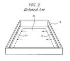
- FIG. 2is a schematic perspective view showing a side flow type apparatus including a chamber according to the related art.
- the injection slit 12 and the exhaust slit 14 facing each otheris formed through the sidewall of the chamber 10 .
- the injection slit 12 and the exhaust slit 14are horizontally disposed with a height of about 2 mm.
- a pressure of the reaction gasesvaries with position in the chamber 10 .
- the variation of the pressure of the reaction gasescauses a variation in amount of injected gases and in amount of exhausted gases, thereby causing a non-uniformity in the plasma treatment process.
- a filmis not uniformly deposited on the substrate 2 or a film on the substrate 2 is not uniformly etched.
- the reaction gasesare supplied to the chamber 10 through the inlet pipe 16 . Since the inlet pipe 16 has a width narrower than the injection slit 12 , the reaction gases are abruptly diffused into chamber 10 at the injection slit 12 . Accordingly, the reaction gases are not uniformly distributed in the chamber 10 and the pressure of the distributed reaction gases varies with position in the chamber 10 . As a result, the amount of the distributed reaction gases varies with position in the chamber, which causes a non-uniformity in the plasma treatment process.
- the processed reaction gasesare evacuated through the outlet pipe 18 having a width narrower than the exhaust slit 14 , the processed reaction gases are abruptly concentrated into the exhaust slit 14 . Accordingly, the processed reaction gases are not uniformly evacuated from the chamber 10 and the pressure variation of the reaction gas with position in the chamber 10 is enlarged. As a result, the variation in the amount of the reaction gases and the non-uniformity in the plasma treatment process increases. The non-uniformity in the plasma treatment process results in deterioration of the thin film and causes deterioration in display quality of the LCD device.
- the present inventionis directed to an apparatus for fabricating a semiconductor device that substantially obviates one or more of the problems due to limitations and disadvantages of the related art.
- an apparatus for fabricating a semiconductor deviceincludes: a chamber having a sidewall; a susceptor in the chamber; a plurality of injection holes in the sidewall, the plurality of injection holes disposed along a horizontal direction; and a plurality of exhaust holes in the sidewall, the plurality of exhaust holes disposed along the horizontal direction and facing the plurality of injection holes with the susceptor therebetween.
- an apparatus for fabricating a semiconductor deviceincludes a chamber having a plurality of injection holes and a plurality of exhaust holes for transport of reaction gases through the chamber in a flow direction from the plurality of injection holes toward the plurality of exhaust holes; gas supply apparatus and gas exhaust apparatus coupled to the chamber; and first structure in communication with the plurality of injection holes and the gas supply apparatus and second structure in communication with the plurality of exhaust holes and the gas exhaust apparatus, wherein the first and second structure change the flow of the reaction gas with respect to the flow direction.
- FIG. 1is a schematic cross-sectional view showing a side flow type apparatus including a chamber according to the related art
- FIG. 2is a schematic perspective view showing a side flow type apparatus including a chamber according to the related art
- FIG. 3is a schematic cross-sectional view of an apparatus according to an exemplary embodiment of the present invention.
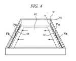
- FIG. 4is a perspective view of an apparatus according to an exemplary embodiment of the present invention.
- FIG. 5Ais a schematic cross-sectional view taken along a line “Va-Va” of FIG. 4 ;
- FIG. 5Bis a schematic cross-sectional view taken along a line “Vb-Vb” of FIG. 4 .
- FIGS. 3 and 4are a schematic cross-sectional view and a schematic perspective view of an apparatus according to an exemplary embodiment of the present invention.
- a side flow type apparatusincludes a chamber 50 , an upper electrode 60 and a lower electrode 70 .
- the chamber 50is a vacuum reaction space isolated from the exterior surroundings, and the upper and lower electrodes 60 and 70 are disposed in the chamber 50 .
- the upper and lower electrodes 60 and 70face each other with a substrate 2 disposed therebetween.
- the upper electrode 60may include a backing plate 62 functioning as one electrode for generating and maintaining plasma.
- the lower electrode 70may include a susceptor 82 functioning as the other electrode for generating and maintaining the plasma.
- the susceptor 82may include a metallic material such as aluminum (Al) or a graphite material coated with aluminum (Al) for grounding.
- a radio frequency (RF) powermay be applied between the upper and lower electrodes 60 and 70 .
- the lower electrode 70may function as a chuck supporting the substrate 2 .
- the apparatustreats the substrate 2 using reaction gases supplied to the chamber 50 .
- the reaction gasesare supplied to the chamber 50 .
- the reaction gasesare excited to form a plasma by an electric field generated between the upper and lower electrodes 60 and 70 .
- the plasmamay react with the substrate 2 or a thin film on the substrate 2 during a plasma treatment process.
- the plasmamay react with the substrate 2 to form a thin film on the substrate 2 .
- the plasmamay react with a thin film on the substrate 2 to pattern the thin film.
- a plurality of injection holes 52 and a plurality of exhaust holes 54are formed in a sidewall of the chamber 50 .
- the plurality of injection holes 52are spaced apart from each other along a horizontal direction by a substantially equal distance.
- the plurality of exhaust holes 54are spaced apart from each other by a substantially equal distance.
- the plurality of injection holes 52 and the plurality of exhaust holes 54may have substantially the same shape and the same size.
- the plurality of injection holes 52 and the plurality of exhaust holes 54face each other, and the substrate 2 is disposed between the plurality of injection holes 52 and the plurality of exhaust holes 54 .
- Each injection hole 52 and each exhaust hole 54have a standing rectangular shape such that a height “H” is greater than a width “W.”
- each injection hole 52 and each exhaust hole 54may have a height within a range of about 2.0 mm to about 6.0 mm, a width within a range of about 1.5 mm to about 5.5 mm and a spaced distance within a range of about 20.5 to about 24.5 mm.
- each injection hole 52 and each exhaust hole 54may have a height of about 4.2 mm, a width of about 3.5 mm and a spaced distance of about 20.5 mm.
- each injection hole 52is connected to a first buffer cavity 56 in the sidewall of the chamber 50 and each exhaust hole 54 is connected to a second buffer cavity 58 in the sidewall of the chamber 50 . Accordingly, the reaction gases supplied to the chamber 50 are injected into the chamber 50 through the first buffer cavity 56 and the plurality of injection holes 52 , flow along a top surface of the substrate 2 and are exhausted out of the chamber 50 through the plurality of exhaust holes 54 and the second buffer cavity 58 .
- the first buffer cavity 56may be connected to a gas supply system (not shown) through an inlet pipe 92 and the second buffer cavity 58 is connected to a vacuum system (not shown) such as a pump through an output pipe 18 .
- the first and second buffer cavities 56 and 58may be bent to change a flow path of the reaction gases.
- the first buffer cavity 56may change an input flow path of the reaction gases upwardly and horizontally. Accordingly, the reaction gases supplied from the exterior flow through the first buffer cavity 56 sequentially along a horizontal direction, an upward direction and a horizontal direction. Then, the reaction gases are injected into the chamber 50 through the plurality of injection holes 52 .
- the second buffer cavity 58may change an output flow path of the reaction gases upwardly, horizontally and downwardly. Accordingly, the reaction gases processed in the chamber 50 flow through the second buffer cavity 58 sequentially along a horizontal direction, an upward direction, a horizontal direction, a downward direction and a horizontal direction. Then, the reaction gases are exhausted through the plurality of exhaust holes 54 .
- the reaction gasesare uniformly diffused in the first buffer cavity 56 .
- the reaction gasesare concentrated in the second buffer cavity 58 . Accordingly, a uniformity of the pressure of the distributed reaction gases and the processed reaction gases is improved.
- FIG. 5Ais a schematic cross-sectional view taken along a line “Va-Va” of FIG. 4 and FIG. 5B is a schematic cross-sectional view taken along a line “Vb-Vb” of FIG. 4 .
- the reaction gases supplied from the exteriorare diffused in the first buffer cavity 56 to increase the pressure uniformity.
- the reaction gases having passed through the first buffer cavity 56are injected into the chamber 50 through the plurality of injection holes 52 .
- the reaction gases flowing to a blocking portion between two adjacent injection holes 52are substantially equally distributed to the two adjacent injection holes 52 . Accordingly, the reaction gases are uniformly distributed by all the plurality of injection holes 52 and the uniformity of the reaction gases further increases. As a result, an injection uniformity of the reaction gases is improved.
- the reaction gases processed in the chamber 50are exhausted to the second buffer cavity 58 through the plurality of exhaust holes 54 .
- the reaction gases flowing to a blocking portion between two adjacent exhaust holes 54are substantially equally distributed to the two adjacent exhaust holes 54 . Accordingly, the reaction gases are uniformly distributed to by all the plurality of exhaust holes 54 . Then, the reaction gases are concentrated in the second buffer cavity 58 and evacuated out of the chamber 50 . Since the reaction gases are exhausted through the plurality of exhaust holes 54 , the exhaust uniformity of the reaction gases are improved.
- the first and second buffer cavities 56 and 58are formed in the sidewall of the chamber 50 in the embodiment illustrated in FIGS. 5A and 5B
- an additional meanssuch as a baffle may be formed inside the sidewall of the chamber 50 .
- the side flow type apparatusmay include not only a chemical vapor deposition (CVD) apparatus and a dry etching apparatus, but also the other kinds of apparatus for fabricating an LCD device having a side flow type.
- a pressure of reaction gasesis kept uniform regardless of positions in a chamber.
- a fabrication process in the apparatussuch as deposition of a thin film and etch of a thin film has an improved uniformity and reliability, thereby obtaining an improved semiconductor device.
Landscapes
- Chemical & Material Sciences (AREA)
- Engineering & Computer Science (AREA)
- Physics & Mathematics (AREA)
- Analytical Chemistry (AREA)
- Plasma & Fusion (AREA)
- Materials Engineering (AREA)
- Metallurgy (AREA)
- Organic Chemistry (AREA)
- Mechanical Engineering (AREA)
- Chemical Kinetics & Catalysis (AREA)
- General Chemical & Material Sciences (AREA)
- Nonlinear Science (AREA)
- Crystallography & Structural Chemistry (AREA)
- General Physics & Mathematics (AREA)
- Optics & Photonics (AREA)
- Drying Of Semiconductors (AREA)
- Chemical Vapour Deposition (AREA)
Abstract
Description
Claims (15)
Applications Claiming Priority (3)
| Application Number | Priority Date | Filing Date | Title |
|---|---|---|---|
| KR2004-050174 | 2004-06-30 | ||
| KR1020040050174AKR101033123B1 (en) | 2004-06-30 | 2004-06-30 | Chamber type device for manufacturing liquid crystal display |
| KR10-2004-0050174 | 2004-06-30 |
Publications (2)
| Publication Number | Publication Date |
|---|---|
| US20060001848A1 US20060001848A1 (en) | 2006-01-05 |
| US8506710B2true US8506710B2 (en) | 2013-08-13 |
Family
ID=35513494
Family Applications (1)
| Application Number | Title | Priority Date | Filing Date |
|---|---|---|---|
| US11/158,395Expired - Fee RelatedUS8506710B2 (en) | 2004-06-30 | 2005-06-22 | Apparatus for fabricating semiconductor device |
Country Status (2)
| Country | Link |
|---|---|
| US (1) | US8506710B2 (en) |
| KR (1) | KR101033123B1 (en) |
Families Citing this family (9)
| Publication number | Priority date | Publication date | Assignee | Title |
|---|---|---|---|---|
| KR101033123B1 (en)* | 2004-06-30 | 2011-05-11 | 엘지디스플레이 주식회사 | Chamber type device for manufacturing liquid crystal display |
| KR100568838B1 (en)* | 2004-08-03 | 2006-04-10 | 주식회사 디엠에스 | Gas injection nozzle and ejector and plasma ashing device using the same |
| JP5432686B2 (en)* | 2009-12-03 | 2014-03-05 | 東京エレクトロン株式会社 | Plasma processing equipment |
| JP5927619B2 (en)* | 2010-05-06 | 2016-06-01 | エヴァテック・アクチェンゲゼルシャフトEvatec Ag | Plasma reactor |
| US9738976B2 (en)* | 2013-02-27 | 2017-08-22 | Ioxus, Inc. | Energy storage device assembly |
| KR102201882B1 (en)* | 2013-12-27 | 2021-01-12 | 세메스 주식회사 | Apparatus and method for treating substrate |
| US12281385B2 (en)* | 2015-06-15 | 2025-04-22 | Taiwan Semiconductor Manufacturing Co., Ltd. | Gas dispenser and deposition apparatus using the same |
| TWI833954B (en)* | 2019-05-28 | 2024-03-01 | 美商應用材料股份有限公司 | Apparatus for improved flow control in process chambers |
| CN112331595B (en)* | 2020-11-30 | 2024-03-26 | 北京北方华创微电子装备有限公司 | Semiconductor processing equipment |
Citations (23)
| Publication number | Priority date | Publication date | Assignee | Title |
|---|---|---|---|---|
| US3805736A (en)* | 1971-12-27 | 1974-04-23 | Ibm | Apparatus for diffusion limited mass transport |
| US4817558A (en)* | 1986-07-10 | 1989-04-04 | Kabushiki Kaisha Toshiba | Thin-film depositing apparatus |
| US5269847A (en)* | 1990-08-23 | 1993-12-14 | Applied Materials, Inc. | Variable rate distribution gas flow reaction chamber |
| US5704981A (en)* | 1995-04-05 | 1998-01-06 | Tokyo Electron Ltd. | Processing apparatus for substrates to be processed |
| US5710486A (en)* | 1995-05-08 | 1998-01-20 | Applied Materials, Inc. | Inductively and multi-capacitively coupled plasma reactor |
| US5916369A (en)* | 1995-06-07 | 1999-06-29 | Applied Materials, Inc. | Gas inlets for wafer processing chamber |
| US5962085A (en)* | 1991-02-25 | 1999-10-05 | Symetrix Corporation | Misted precursor deposition apparatus and method with improved mist and mist flow |
| KR200173020Y1 (en) | 1996-12-28 | 2000-03-02 | 김영환 | Lower pressure chemical vapor deposition (lpcvd) |
| US6070551A (en)* | 1996-05-13 | 2000-06-06 | Applied Materials, Inc. | Deposition chamber and method for depositing low dielectric constant films |
| US6143081A (en)* | 1996-07-12 | 2000-11-07 | Tokyo Electron Limited | Film forming apparatus and method, and film modifying apparatus and method |
| US6444039B1 (en)* | 2000-03-07 | 2002-09-03 | Simplus Systems Corporation | Three-dimensional showerhead apparatus |
| US20030049372A1 (en)* | 1997-08-11 | 2003-03-13 | Cook Robert C. | High rate deposition at low pressures in a small batch reactor |
| US20030192646A1 (en)* | 2002-04-12 | 2003-10-16 | Applied Materials, Inc. | Plasma processing chamber having magnetic assembly and method |
| KR20040014760A (en) | 2002-08-12 | 2004-02-18 | 주성엔지니어링(주) | Semiconductor device fabrication apparatus having multi-hole angled gas injection system and semiconductor device fabrication method using the same |
| US6709523B1 (en)* | 1999-11-18 | 2004-03-23 | Tokyo Electron Limited | Silylation treatment unit and method |
| US20060001848A1 (en)* | 2004-06-30 | 2006-01-05 | Lg Philips Lcd Co., Ltd. | Apparatus for fabricating semiconductor device |
| US20060275546A1 (en)* | 2005-06-02 | 2006-12-07 | Arena Chantal J | Apparatus and methods for isolating chemical vapor reactions at a substrate surface |
| US20090148704A1 (en)* | 2007-12-11 | 2009-06-11 | Sumitomo Electric Industries, Ltd. | Vapor-phase process apparatus, vapor-phase process method, and substrate |
| US20100092668A1 (en)* | 2008-10-10 | 2010-04-15 | Alta Devices, Inc. | Concentric Showerhead For Vapor Deposition |
| US20120240853A1 (en)* | 2011-03-22 | 2012-09-27 | Applied Materials, Inc. | Liner assembly for chemical vapor deposition chamber |
| US8282768B1 (en)* | 2005-04-26 | 2012-10-09 | Novellus Systems, Inc. | Purging of porogen from UV cure chamber |
| US8337619B2 (en)* | 2008-09-19 | 2012-12-25 | Applied Materials, Inc. | Polymeric coating of substrate processing system components for contamination control |
| US8398816B1 (en)* | 2006-03-28 | 2013-03-19 | Novellus Systems, Inc. | Method and apparatuses for reducing porogen accumulation from a UV-cure chamber |
Family Cites Families (1)
| Publication number | Priority date | Publication date | Assignee | Title |
|---|---|---|---|---|
| US6171326B1 (en)* | 1998-08-27 | 2001-01-09 | Micrus Corporation | Three dimensional, low friction vasoocclusive coil, and method of manufacture |
- 2004
- 2004-06-30KRKR1020040050174Apatent/KR101033123B1/ennot_activeExpired - Fee Related
- 2005
- 2005-06-22USUS11/158,395patent/US8506710B2/ennot_activeExpired - Fee Related
Patent Citations (25)
| Publication number | Priority date | Publication date | Assignee | Title |
|---|---|---|---|---|
| US3805736A (en)* | 1971-12-27 | 1974-04-23 | Ibm | Apparatus for diffusion limited mass transport |
| US4817558A (en)* | 1986-07-10 | 1989-04-04 | Kabushiki Kaisha Toshiba | Thin-film depositing apparatus |
| US5269847A (en)* | 1990-08-23 | 1993-12-14 | Applied Materials, Inc. | Variable rate distribution gas flow reaction chamber |
| US5962085A (en)* | 1991-02-25 | 1999-10-05 | Symetrix Corporation | Misted precursor deposition apparatus and method with improved mist and mist flow |
| US5704981A (en)* | 1995-04-05 | 1998-01-06 | Tokyo Electron Ltd. | Processing apparatus for substrates to be processed |
| US5710486A (en)* | 1995-05-08 | 1998-01-20 | Applied Materials, Inc. | Inductively and multi-capacitively coupled plasma reactor |
| US5916369A (en)* | 1995-06-07 | 1999-06-29 | Applied Materials, Inc. | Gas inlets for wafer processing chamber |
| US6070551A (en)* | 1996-05-13 | 2000-06-06 | Applied Materials, Inc. | Deposition chamber and method for depositing low dielectric constant films |
| US6143081A (en)* | 1996-07-12 | 2000-11-07 | Tokyo Electron Limited | Film forming apparatus and method, and film modifying apparatus and method |
| KR200173020Y1 (en) | 1996-12-28 | 2000-03-02 | 김영환 | Lower pressure chemical vapor deposition (lpcvd) |
| US20030049372A1 (en)* | 1997-08-11 | 2003-03-13 | Cook Robert C. | High rate deposition at low pressures in a small batch reactor |
| US6709523B1 (en)* | 1999-11-18 | 2004-03-23 | Tokyo Electron Limited | Silylation treatment unit and method |
| US6444039B1 (en)* | 2000-03-07 | 2002-09-03 | Simplus Systems Corporation | Three-dimensional showerhead apparatus |
| US20030192646A1 (en)* | 2002-04-12 | 2003-10-16 | Applied Materials, Inc. | Plasma processing chamber having magnetic assembly and method |
| KR20040014760A (en) | 2002-08-12 | 2004-02-18 | 주성엔지니어링(주) | Semiconductor device fabrication apparatus having multi-hole angled gas injection system and semiconductor device fabrication method using the same |
| US20060001848A1 (en)* | 2004-06-30 | 2006-01-05 | Lg Philips Lcd Co., Ltd. | Apparatus for fabricating semiconductor device |
| US8282768B1 (en)* | 2005-04-26 | 2012-10-09 | Novellus Systems, Inc. | Purging of porogen from UV cure chamber |
| US20060275546A1 (en)* | 2005-06-02 | 2006-12-07 | Arena Chantal J | Apparatus and methods for isolating chemical vapor reactions at a substrate surface |
| US8398816B1 (en)* | 2006-03-28 | 2013-03-19 | Novellus Systems, Inc. | Method and apparatuses for reducing porogen accumulation from a UV-cure chamber |
| US20090148704A1 (en)* | 2007-12-11 | 2009-06-11 | Sumitomo Electric Industries, Ltd. | Vapor-phase process apparatus, vapor-phase process method, and substrate |
| US20120024227A1 (en)* | 2007-12-11 | 2012-02-02 | Sumitomo Electric Industries, Ltd. | Vapor-phase process apparatus, vapor-phase process method, and substrate |
| US8349403B2 (en)* | 2007-12-11 | 2013-01-08 | Sumitomo Electric Industries, Ltd. | Vapor-phase process apparatus, vapor-phase process method, and substrate |
| US8337619B2 (en)* | 2008-09-19 | 2012-12-25 | Applied Materials, Inc. | Polymeric coating of substrate processing system components for contamination control |
| US20100092668A1 (en)* | 2008-10-10 | 2010-04-15 | Alta Devices, Inc. | Concentric Showerhead For Vapor Deposition |
| US20120240853A1 (en)* | 2011-03-22 | 2012-09-27 | Applied Materials, Inc. | Liner assembly for chemical vapor deposition chamber |
Non-Patent Citations (1)
| Title |
|---|
| Office Action issued in corresponding Korean Patent Application No. 10-2004-0050174, mailed Dec. 20, 2010. |
Also Published As
| Publication number | Publication date |
|---|---|
| KR101033123B1 (en) | 2011-05-11 |
| US20060001848A1 (en) | 2006-01-05 |
| KR20060001140A (en) | 2006-01-06 |
Similar Documents
| Publication | Publication Date | Title |
|---|---|---|
| KR100658239B1 (en) | Gas diffusion shower head design for large area plasma enhanced chemical vapor deposition | |
| KR100253134B1 (en) | Substrate Processing Equipment | |
| JP3366301B2 (en) | Plasma CVD equipment | |
| US5704981A (en) | Processing apparatus for substrates to be processed | |
| US20090229754A1 (en) | Shower head and substrate processing apparatus | |
| US20090165722A1 (en) | Apparatus for treating substrate | |
| US20110024527A1 (en) | Gas injector and apparatus including the same | |
| US20080044321A1 (en) | Power supply unit for generating plasma and plasma apparatus including the same | |
| KR20070091589A (en) | Uniform Plasma Control by Gas Diffusion Hole Structure | |
| US8506710B2 (en) | Apparatus for fabricating semiconductor device | |
| US20050034673A1 (en) | Apparatus having edge frame and method of using the same | |
| JP2004327767A (en) | Plasma processing apparatus | |
| JPH08260158A (en) | Substrate processing equipment | |
| US20070283889A1 (en) | Apparatus of processing substrate | |
| KR20080048243A (en) | Plasma Chemical Vapor Deposition System | |
| US10600610B2 (en) | Substrate treatment apparatus | |
| US20080128088A1 (en) | Etching apparatus for edges of substrate | |
| KR20170102778A (en) | Apparatus for processing substrate | |
| CN110846636A (en) | Coating material for processing chamber | |
| KR102766065B1 (en) | Apparatus for processing substrate | |
| KR101119798B1 (en) | Chemical vapor deposition system | |
| KR100941959B1 (en) | Thin film deposition apparatus for liquid crystal display | |
| JP2002329711A (en) | Parallel plate type electrode plasma processing equipment | |
| KR20080105525A (en) | Thin film formation method including silicon | |
| KR101248928B1 (en) | Substrate processing apparatus improving temperature gradient between chamber and exhaust line |
Legal Events
| Date | Code | Title | Description |
|---|---|---|---|
| AS | Assignment | Owner name:LG. PHILIPS LCD CO., LTD., KOREA, REPUBLIC OF Free format text:ASSIGNMENT OF ASSIGNORS INTEREST;ASSIGNOR:HWANG, JUNG-WOO;REEL/FRAME:016719/0378 Effective date:20050620 | |
| AS | Assignment | Owner name:LG DISPLAY CO. LTD.,KOREA, REPUBLIC OF Free format text:CHANGE OF NAME;ASSIGNOR:LG. PHILIPS LCD CO., LTD.;REEL/FRAME:020976/0243 Effective date:20080229 Owner name:LG DISPLAY CO. LTD., KOREA, REPUBLIC OF Free format text:CHANGE OF NAME;ASSIGNOR:LG. PHILIPS LCD CO., LTD.;REEL/FRAME:020976/0243 Effective date:20080229 | |
| STCF | Information on status: patent grant | Free format text:PATENTED CASE | |
| FEPP | Fee payment procedure | Free format text:PAYOR NUMBER ASSIGNED (ORIGINAL EVENT CODE: ASPN); ENTITY STATUS OF PATENT OWNER: LARGE ENTITY | |
| FPAY | Fee payment | Year of fee payment:4 | |
| FEPP | Fee payment procedure | Free format text:MAINTENANCE FEE REMINDER MAILED (ORIGINAL EVENT CODE: REM.); ENTITY STATUS OF PATENT OWNER: LARGE ENTITY | |
| LAPS | Lapse for failure to pay maintenance fees | Free format text:PATENT EXPIRED FOR FAILURE TO PAY MAINTENANCE FEES (ORIGINAL EVENT CODE: EXP.); ENTITY STATUS OF PATENT OWNER: LARGE ENTITY | |
| STCH | Information on status: patent discontinuation | Free format text:PATENT EXPIRED DUE TO NONPAYMENT OF MAINTENANCE FEES UNDER 37 CFR 1.362 | |
| FP | Lapsed due to failure to pay maintenance fee | Effective date:20210813 |