US8502796B1 - Interpolated single-layer touch sensor - Google Patents
Interpolated single-layer touch sensorDownload PDFInfo
- Publication number
- US8502796B1 US8502796B1US13/595,595US201213595595AUS8502796B1US 8502796 B1US8502796 B1US 8502796B1US 201213595595 AUS201213595595 AUS 201213595595AUS 8502796 B1US8502796 B1US 8502796B1
- Authority
- US
- United States
- Prior art keywords
- electrodes
- electrode
- touch sensor
- electrode line
- length along
- Prior art date
- Legal status (The legal status is an assumption and is not a legal conclusion. Google has not performed a legal analysis and makes no representation as to the accuracy of the status listed.)
- Expired - Fee Related
Links
Images


Classifications
- G—PHYSICS
- G06—COMPUTING OR CALCULATING; COUNTING
- G06F—ELECTRIC DIGITAL DATA PROCESSING
- G06F3/00—Input arrangements for transferring data to be processed into a form capable of being handled by the computer; Output arrangements for transferring data from processing unit to output unit, e.g. interface arrangements
- G06F3/01—Input arrangements or combined input and output arrangements for interaction between user and computer
- G06F3/03—Arrangements for converting the position or the displacement of a member into a coded form
- G06F3/041—Digitisers, e.g. for touch screens or touch pads, characterised by the transducing means
- G06F3/0416—Control or interface arrangements specially adapted for digitisers
- G06F3/04164—Connections between sensors and controllers, e.g. routing lines between electrodes and connection pads
- G—PHYSICS
- G06—COMPUTING OR CALCULATING; COUNTING
- G06F—ELECTRIC DIGITAL DATA PROCESSING
- G06F3/00—Input arrangements for transferring data to be processed into a form capable of being handled by the computer; Output arrangements for transferring data from processing unit to output unit, e.g. interface arrangements
- G06F3/01—Input arrangements or combined input and output arrangements for interaction between user and computer
- G06F3/03—Arrangements for converting the position or the displacement of a member into a coded form
- G06F3/041—Digitisers, e.g. for touch screens or touch pads, characterised by the transducing means
- G06F3/044—Digitisers, e.g. for touch screens or touch pads, characterised by the transducing means by capacitive means
- G06F3/0443—Digitisers, e.g. for touch screens or touch pads, characterised by the transducing means by capacitive means using a single layer of sensing electrodes
- G—PHYSICS
- G06—COMPUTING OR CALCULATING; COUNTING
- G06F—ELECTRIC DIGITAL DATA PROCESSING
- G06F3/00—Input arrangements for transferring data to be processed into a form capable of being handled by the computer; Output arrangements for transferring data from processing unit to output unit, e.g. interface arrangements
- G06F3/01—Input arrangements or combined input and output arrangements for interaction between user and computer
- G06F3/03—Arrangements for converting the position or the displacement of a member into a coded form
- G06F3/041—Digitisers, e.g. for touch screens or touch pads, characterised by the transducing means
- G06F3/044—Digitisers, e.g. for touch screens or touch pads, characterised by the transducing means by capacitive means
- G06F3/0448—Details of the electrode shape, e.g. for enhancing the detection of touches, for generating specific electric field shapes, for enhancing display quality
- G—PHYSICS
- G06—COMPUTING OR CALCULATING; COUNTING
- G06F—ELECTRIC DIGITAL DATA PROCESSING
- G06F2203/00—Indexing scheme relating to G06F3/00 - G06F3/048
- G06F2203/041—Indexing scheme relating to G06F3/041 - G06F3/045
- G06F2203/04112—Electrode mesh in capacitive digitiser: electrode for touch sensing is formed of a mesh of very fine, normally metallic, interconnected lines that are almost invisible to see. This provides a quite large but transparent electrode surface, without need for ITO or similar transparent conductive material
- G—PHYSICS
- G06—COMPUTING OR CALCULATING; COUNTING
- G06F—ELECTRIC DIGITAL DATA PROCESSING
- G06F3/00—Input arrangements for transferring data to be processed into a form capable of being handled by the computer; Output arrangements for transferring data from processing unit to output unit, e.g. interface arrangements
- G06F3/01—Input arrangements or combined input and output arrangements for interaction between user and computer
- G06F3/03—Arrangements for converting the position or the displacement of a member into a coded form
- G06F3/041—Digitisers, e.g. for touch screens or touch pads, characterised by the transducing means
- G06F3/0412—Digitisers structurally integrated in a display
Definitions
- This disclosuregenerally relates to touch sensors.
- An array of conductive drive and sense electrodesmay form a mutual-capacitance touch sensor having one or more capacitive nodes.
- the mutual-capacitance touch sensormay have either a two-layer configuration or single-layer configuration.
- drive and sense electrodesmay be disposed in a pattern on one side of a substrate. In such a configuration, a pair of drive and sense electrodes capacitively coupled to each other across a space or dielectric between electrodes may form a capacitive node.
- an array of vertical and horizontal conductive electrodesmay be disposed in a pattern on one side of the substrate.
- Each of the conductive electrodes in the arraymay form a capacitive node, and, when an object touches or comes within proximity of the electrode, a change in self-capacitance may occur at that capacitive node and a controller may measure the change in capacitance as a change in voltage or a change in the amount of charge needed to raise the voltage to some pre-determined amount.
- a touch sensordetects the presence and location of a touch or the proximity of an object (such as a user's finger or a stylus) within a touch-sensitive area of the touch sensor overlaid, for example, on a display screen.
- the touch sensorenables a user to interact directly with what is displayed on the screen, rather than indirectly with a mouse or touchpad.
- a touch sensormay be attached to or provided as part of a desktop computer, laptop computer, tablet computer, personal digital assistant (PDA), smartphone, satellite navigation device, portable media player, portable game console, kiosk computer, point-of-sale device, or other suitable device.
- a control panel on a household or other appliancemay include a touch sensor.
- touch sensorssuch as resistive touch screens, surface acoustic wave touch screens, capacitive touch screens, infrared touch screens, and optical touch screens.
- reference to a touch sensorencompasses a touch screen, and vice versa, where appropriate.
- a capacitive touch screenmay include an insulator coated with a substantially transparent conductor in a particular pattern.
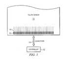
- FIG. 1illustrates a touch sensor with an example controller, according to example embodiments
- FIGS. 2A-2Cillustrate patterns for the touch sensor of FIG. 1 , according to example embodiments
- FIGS. 3A and 3Billustrate another pattern for the touch sensor of FIG. 1 , according to example embodiments.
- FIG. 4illustrates a touch sensor of FIGS. 2A-2C having a central spine, according to example embodiments.
- FIG. 1illustrates an example touch sensor 10 with an example controller 12 .
- a touch sensormay encompass a touch screen, and vice versa, where appropriate.
- Touch sensor 10 and controller 12detect the presence and location of a touch or the proximity of an object within a touch-sensitive area of touch sensor 10 .
- reference to a touch sensorencompasses both the touch sensor and its controller, where appropriate.
- reference to a controllerencompasses both the controller and its touch sensor, where appropriate.
- Touch sensor 10includes one or more touch-sensitive areas, where appropriate.
- Touch sensor 10includes an array of drive and sense electrodes disposed on a substrate, which in some embodiments is a dielectric material.
- one or more portions of the substrate of touch sensor 10are made of polyethylene terephthalate (PET) or another suitable material.
- PETpolyethylene terephthalate
- the drive or sense electrodes in touch sensor 10are made of indium tin oxide (ITO) in whole or in part.
- the drive or sense electrodes in touch sensor 10are made of fine lines of metal or other conductive material.
- one or more portions of the conductive materialare copper or copper-based and have a thickness of approximately 5 ⁇ m or less and a width of approximately 10 ⁇ m or less.
- one or more portions of the conductive materialare silver or silver-based and similarly have a thickness of approximately 5 ⁇ m or less and a width of approximately 10 ⁇ m or less.
- This disclosurecontemplates any suitable electrodes made of any suitable material.
- touch sensor 10implements a capacitive form of touch sensing.
- touch sensor 10includes an array of drive and sense electrodes forming an array of capacitive nodes.
- a drive electrode and a sense electrodeform a capacitive node.
- the drive and sense electrodes forming the capacitive nodecome near each other, but do not make electrical contact with each other. Instead, the drive and sense electrodes are capacitively coupled to each other across a gap between them.
- a pulsed or alternating voltage applied to the drive electrodei.e., by controller 12 ) induces a charge on the sense electrode, and the amount of charge induced is susceptible to external influence (such as a touch or the proximity of an object).
- controller 12determines the position of the touch or proximity within the touch-sensitive area(s) of touch sensor 10 .
- one or more drive electrodestogether form a drive line running horizontally or vertically or in any suitable orientation.
- one or more sense electrodestogether form a sense line running horizontally or vertically or in any suitable orientation.
- drive linesrun substantially perpendicular to sense lines.
- reference to a drive lineencompasses one or more drive electrodes making up the drive line, and vice versa, where appropriate.
- reference to a sense lineencompasses one or more sense electrodes making up the sense line, and vice versa, where appropriate.
- touch sensor 10has a single-layer configuration, with drive and sense electrodes disposed in a pattern on one side of a substrate.
- a pair of drive and sense electrodes capacitively coupled to each other across a space between themforms a capacitive node.
- electrodes of only a single typee.g. drive
- this disclosuredescribes particular configurations of particular electrodes forming particular nodes, this disclosure contemplates any suitable configuration of any suitable electrodes forming any suitable nodes.
- this disclosurecontemplates any suitable electrodes disposed on any suitable number of any suitable substrates in any suitable patterns.
- a change in capacitance at a capacitive node of touch sensor 10may indicate a touch or proximity input at the position of the capacitive node.
- Controller 12is operable to detect and process the change in capacitance to determine the presence and location of the touch or proximity input. Certain embodiments if controller 12 communicate information about the touch or proximity input to one or more other components (such one or more central processing units (CPUs) or digital signal processors (DSPs)) of a device that includes touch sensor 10 and controller 12 , which may respond to the touch or proximity input by initiating a function of the device (or an application running on the device) associated with it.
- CPUscentral processing units
- DSPsdigital signal processors
- controller 12is one or more integrated circuits (ICs)—such as for example general-purpose microprocessors, microcontrollers, programmable logic devices or arrays, and application-specific ICs (ASICs).
- controller 12is coupled to a flexible printed circuit (FPC) bonded to the substrate of touch sensor 10 , as described below.
- FPCflexible printed circuit
- controller 12include a processor unit, a drive unit, a sense unit, and a storage unit.
- the drive unitsupplies drive signals to the drive electrodes of touch sensor 10 .
- the sense unitsenses charge at the capacitive nodes of touch sensor 10 and provides measurement signals to the processor unit representing capacitances at the capacitive nodes.
- the processor unitcontrols the supply of drive signals to the drive electrodes by the drive unit and process measurement signals from the sense unit to detect and process the presence and location of a touch or proximity input within the touch-sensitive area(s) of touch sensor 10 .
- the processor unitalso tracks changes in the position of a touch or proximity input within the touch-sensitive area(s) of touch sensor 10 .
- the storage unitwhich includes one or more memory devices, stores programming for execution by the processor unit, including programming for controlling the drive unit to supply drive signals to the drive electrodes, programming for processing measurement signals from the sense unit, and other suitable programming, where appropriate.
- Tracks 14 of conductive material disposed on the substrate of touch sensor 10couple the drive or sense electrodes of touch sensor 10 to connection pads 16 , also disposed on the substrate of touch sensor 10 .
- connection pads 16facilitate coupling of tracks 14 to controller 12 .
- tracks 14extend into or around (e.g. at the edges of) the touch-sensitive area(s) of touch sensor 10 .
- Particular tracks 14provide drive connections for coupling controller 12 to drive electrodes of touch sensor 10 , through which the drive unit of controller 12 supplies drive signals to the drive electrodes.
- Other tracks 14provide sense connections for coupling controller 12 to sense electrodes of touch sensor 10 , through which the sense unit of controller 12 senses charge at the capacitive nodes of touch sensor 10 .
- tracks 14are made of fine lines of metal or other conductive material.
- the conductive material of tracks 14are copper or copper-based and have a width of approximately 100 ⁇ m or less.
- the conductive material of tracks 14are silver or silver-based and have a width of approximately 100 ⁇ m or less.
- tracks 14are made of ITO in whole or in part in addition or as an alternative to fine lines of metal or other conductive material.
- this disclosuredescribes particular tracks made of particular materials with particular widths, this disclosure contemplates any suitable tracks made of any suitable materials with any suitable widths.
- certain embodiments of touch sensor 10include one or more ground lines terminating at a ground connector (similar to a connection pad 16 ) at an edge of the substrate of touch sensor 10 (similar to tracks 14 ).
- connection pads 16are located along one or more edges of the substrate, outside the touch-sensitive area(s) of touch sensor 10 .
- controller 12is on an FPC in certain embodiments.
- connection pads 16are made of the same material as tracks 14 and are bonded to the FPC using an anisotropic conductive film (ACF).
- ACFanisotropic conductive film
- connection 18includes conductive lines on the FPC coupling controller 12 to connection pads 16 , in turn coupling controller 12 to tracks 14 and to the drive or sense electrodes of touch sensor 10 .
- connection pads 160are inserted into an electro-mechanical connector (such as a zero insertion force wire-to-board connector); in this embodiment, connection 180 does not need to include an FPC. This disclosure contemplates any suitable connection 18 between controller 12 and touch sensor 10 .
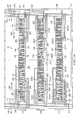
- FIG. 2Aillustrates an example single-layer touch sensor for use in the example system of FIG. 1 .
- touch sensor 10includes an array of one or more drive electrodes 20 A-C and one or more sense electrodes 22 A-III defining a touch-sensitive area of touch sensor 10 .
- Each row 23 of the arrayincludes a drive electrode 20 A-C extending at alternating angles 25 to an axis 21 corresponding to rows 23 of the array.
- Each row 23also includes one or more sense electrodes 22 A-III disposed adjacent to a corresponding drive electrode 20 A-C.
- row 23 A of the arrayincludes drive electrode 20 A with corresponding sense electrodes 22 A-I disposed adjacent to drive electrode 20 A.
- One or more sense electrodes 22 A-III commonly coupled to a track 14define columns 27 A-B that are substantially perpendicular to rows 23 of the array.
- sense electrodes 22 F, 22 FF and 22 FFF commonly coupled to track 14 Fdefine part of column 27 b of the array.
- each drive electrode 20 A-Cis capacitively coupled to one or more adjacent sense electrodes 22 A-III separated by a gap 32 .
- An electrodeis an area of conductive material forming a shape, such as for example a disc, square, rectangle, other suitable shape, or suitable combination of these.
- the conductive material of an electrodee.g., 22 A and 20 C
- the conductive material of an electrodeoccupies approximately 100% of the area of its shape.
- drive and sense electrodes e.g., 22 A and 20 C, along with electrode connectors, e.g., 24 Iare made of indium tin oxide (ITO) and the ITO of the drive and sense electrodes, e.g., 22 A and 20 C, occupies approximately 100% of the area of its shape, where appropriate.
- ITOindium tin oxide
- the conductive material of an electrodeoccupies approximately 50% of the area of its shape.
- an electrodee.g., 22 A and 20 C
- the conductive material of an electrode, e.g., 22 A and 20 Coccupies approximately 5% of the area of its shape.
- an electrodee.g., 22 A and 20 C
- this disclosuredescribes or illustrates particular electrodes made of particular conductive material forming particular shapes with particular fills having particular patterns, this disclosure contemplates any suitable electrodes made of any suitable conductive material forming any suitable shapes with any suitable fills having any suitable patterns.
- the shapes of the electrodes (or other elements) of a touch sensorconstitute in whole or in part one or more macro-features of certain embodiments of the touch sensor.
- One or more characteristics of the implementation of those shapesconstitute in whole or in part one or more micro-features of certain embodiments of the touch sensor.
- drive electrodes 20 A-C and sense electrodes 22 A-IIIinclude individual electrodes 34 or “teeth” that protrude from main electrode lines (e.g., electrode lines 35 as illustrated in FIGS. 2B and 2C ).
- Certain embodiments of electrodes 34 of each sense electrode 22 A-IIIare adjacent to an electrode 34 of a corresponding drive electrode 20 A-C forming capacitive coupling edges separated by gap 32 .
- Electrodes 34may be interleaved or interdigitated to increase the number of capacitive coupling edges between one or more sense electrodes and a corresponding drive electrode.
- electrodes 34 of sense electrodes 22 CCC and 22 GGGare interdigitated with electrodes 34 of corresponding drive electrode 20 C.
- Capacitive coupling between sense electrode and corresponding drive electrodeis determined by dimensions of gap 32 and edges of electrodes 34 .
- gap 32is substantially uniform (e.g., gap 32 between drive electrodes 20 A-C and sense electrodes 22 A-III and their corresponding electrodes 34 is substantially the same width). In other embodiments, gap 32 may not be uniform.
- certain embodimentsinclude drive electrodes 20 A-C, sense electrodes 22 A-III, and electrodes 34 that have substantially similar widths (e.g., the widths of electrodes 34 and electrode lines 35 of drive electrodes 20 A-C and sense electrodes 22 A-III are substantially the same).
- drive electrodes 20 A-C, sense electrodes 22 A-III, and electrodes 34do not have substantially similar widths (e.g., the widths of electrodes 34 and electrode lines 35 of drive electrodes 20 A-C and sense electrodes 22 A-III are not substantially the same).
- this disclosuredescribes and illustrates a particular arrangement of electrodes for touch sensor 10 , this disclosure contemplates any suitable arrangement of electrodes for touch sensor 10 .
- the width of the discrete pieces of material forming the various portions of drive electrodes 20 A-C, sense electrodes 22 A-III, electrodes 34 , electrode lines 35 , etc., and the spacing between those pieces and other portions of touch sensor 10is not uniform. In certain embodiments, the width of those pieces and the spacing between them and other portions of touch sensor 10 is substantially uniform. In embodiments where the width of those pieces and the spacing between them is substantially uniform, visual artifacts are reduced and images viewed through the sensor are affected less than with non-uniform sensors. In such uniform sensor embodiments, the uniformity can be achieved by appropriate design of the various portions of the electrodes of touch sensor 10 and/or by adjusting the spacing between them.
- disconnected pieces of the same material used to form the electrodes of touch sensor 10may be positioned in any open spaces of touch sensor 10 .
- disconnected materialmay be placed in the open space between track 14 E and sense electrode 22 A, in the open space between track 14 G and sense electrode 22 I, in the rectangular open spaces above sense electrodes 22 C, 22 E, and 22 G, in the rectangular open spaces below sense electrodes 22 D and 22 F, and the like.
- open spaces illustrated in FIGS. 2B-2C , 3 A- 3 B, and 4may also be filled with such disconnected material.
- Such disconnected pieces of material used to fill the open spaces of touch sensor 10are not electrically connected to any tracks 14 and do not function as electrodes.
- FIG. 2Bis an enlarged area 50 a of a portion of row 23 A of FIG. 2A .
- FIG. 2Billustrates electrode line 35 A and electrodes 34 A (e.g., 34 A 1 - 34 A 3 ) of sense electrode 22 A, electrode line 35 B and electrodes 34 B (e.g., 34 B 1 - 34 B 3 ) of sense electrode 22 B, and electrode line 35 C and electrodes 34 C (e.g., 34 C 1 - 34 C 3 ) and 34 D (e.g., 34 D 1 - 34 D 3 ) of drive electrode 20 A.
- electrode lines 35 A-C and electrodes 34 A-Dare all disposed on the same side of substrate 15 .
- electrode lines 35 A and 35 Bare substantially parallel to direction 52 , which is parallel to axis 21 and extends between the left and right ends of substrate 15 .
- Electrode line 35 Aincludes electrodes 34 A that protrude from electrode line 35 A and are substantially perpendicular to electrode line 35 A and direction 52 .
- a set of electrodes 34 Adecreases in length along direction 52 .
- electrode 34 A 1which is closest to the left edge of electrode line 35 A, is longer than electrode 34 A 2 .
- Electrode 34 A 2is longer than electrode 34 A 3 , and so forth.
- electrode line 35 Bincludes electrodes 34 B that protrude from electrode line 35 B and are substantially perpendicular to electrode line 35 B and direction 52 .
- a set of electrodes 34 Bincreases in length along direction 52 .
- electrode 34 B 1which is closest to the left edge of electrode line 35 B, is shorter than electrode 34 B 2 .
- Electrode 34 B 2is shorter than electrode 34 B 3 , and so forth.
- Electrode line 35 Cincludes electrodes 34 C that protrude from the top of electrode line 35 C and electrodes 34 D that protrude from the bottom of electrode line 35 C. Electrodes 34 C and 34 D are substantially perpendicular to electrode line 35 C and direction 52 . Electrodes 34 C are interdigitated with electrodes 34 A (i.e., there are alternating electrodes 34 C and 34 A along direction 52 ) and electrodes 34 D are interdigitated with electrodes 34 B (i.e., there are alternating electrodes 34 D and 34 B along direction 52 ). In certain embodiments, a set of electrodes 34 C decreases in length along direction 52 . For example, electrode 34 C 1 , which is closest to the left edge of electrode line 35 C, is longer than electrode 34 C 2 .
- Electrode 34 C 2is longer than electrode 34 C 3 , and so forth.
- a set of electrodes 34 Dincreases in length along direction 52 .
- electrode 34 D 1which is closest to the left edge of electrode line 35 C, is shorter than electrode 34 D 2 .
- Electrode 34 D 2is shorter than electrode 34 D 3 , and so forth.
- FIG. 2Cis an enlarged area 50 b of another portion of row 23 A of FIG. 2A .
- FIG. 2Cillustrates electrode line 35 I and electrodes 34 I (e.g., 34 I 1 - 34 I 3 ) of sense electrode 22 I, electrode line 35 H and electrodes 34 H (e.g., 34 H 1 - 34 H 3 ) of sense electrode 22 H, and electrode line 35 C and electrodes 34 C (e.g., 34 C 1 - 34 C 3 ) and 34 D (e.g., 34 D 1 - 34 D 3 ) of drive electrode 20 A.
- electrode lines 35 and electrodes 34 illustrated in FIG. 2Care all disposed on the same side of substrate 15 .
- electrode lines 35 I and 35 Hare substantially parallel to direction 52 , which is parallel to axis 21 and extends between the left and right ends of substrate 15 .
- Electrode line 35 Iincludes electrodes 34 I that protrude from electrode line 35 I and are substantially perpendicular to electrode line 35 I and direction 52 .
- a set of electrodes 34 Iincreases in length along direction 52 .
- electrode 34 I 3which is closest to the right edge of electrode line 35 I, is longer than electrode 34 I 2 .
- Electrode 34 I 2is longer than electrode 34 I 3 , and so forth.
- electrode line 35 Hincludes electrodes 34 H that protrude from electrode line 35 H and are substantially perpendicular to electrode line 35 H and direction 52 .
- a set of electrodes 34 Hdecreases in length along direction 52 .
- electrode 34 H 3which is closest to the right edge of electrode line 35 H, is shorter than electrode 34 H 2 .
- Electrode 34 H 2is shorter than electrode 34 H 3 , and so forth.
- Electrodes 34 Care interdigitated with electrodes 34 I (i.e., there are alternating electrodes 34 C and 34 I along direction 52 ) and electrodes 34 D are interdigitated with electrodes 34 H (i.e., there are alternating electrodes 34 D and 34 H along direction 52 ).
- a set of electrodes 34 Cincreases in length along direction 52 .
- electrode 34 C 3which is closest to the right edge of electrode line 35 C, is longer than electrode 34 C 2 .
- Electrode 34 C 2is longer than electrode 34 C 3 , and so forth.
- a set of electrodes 34 Ddecreases in length along direction 52 .
- electrode 34 D 1which is closest to the right edge of electrode line 35 C, is shorter than electrode 34 D 2 .
- Electrode 34 D 2is shorter than electrode 34 D 3 , and so forth.
- optical properties of gap 32 as well as voids 36 within other areas of the array with large dimensions relative to feature sizes of drive electrodes 20 A-Cmay have different optical properties than the optical properties of electrodes (either sense electrodes 22 A-IIIor drive electrodes 20 A-C). Optical discontinuities may occur when viewing a display underneath touch sensor 10 due to these differences in optical properties.
- gaps 32 and voids 36 within other areas of the arrayare substantially filled using the conductive material used to fabricate drive electrodes 20 A-C and sense electrodes 22 A-III in such a way to electrically isolate the filled in areas from nearby drive electrodes 20 A-C and sense electrodes 22 A-III or electrode connectors, i.e., 24 A, 24 I, and 26 A.
- gaps 32 and voids 36are substantially filled using “in-fill” shapes of electrode conductive material isolated from neighboring in-fill shapes by non-conducting gaps. The isolated in-fill shapes may serve to visually obscure a pattern of drive electrodes 20 A-C and sense electrodes 22 A-III, while having a minimal impact on the fringing fields between adjacent electrodes.
- using in-fill shapesmay have electric field distributions substantially similar to electric field distributions without in-fill shapes.
- the in-fillingis formed during manufacture and using the same process steps as drive electrodes 20 A-C and sense electrodes 22 A-III, such that in-fill shapes are formed from the same material and have substantially the same thickness and electrical properties as drive electrodes 20 A-C and sense electrodes 22 A-III.
- in-fill shapesreduces a number of areas with optical discontinuities visible when viewing the display.
- in-fill shapesare formed using metal, conductive plastic, ITO, or other form of conductive material, such as fine line metal.
- the material used to fill in a gap 32 or void 36depends on the conductive material used to fabricate drive electrodes 20 A-C and sense electrodes 22 A-III.
- certain embodiments of gaps 32 and voids 36are substantially filled in using a series of electrically isolated squares formed during fabrication of drive electrodes 20 A-C and sense electrodes 22 A-III.
- Drive electrodes 20 A-C and sense electrodes 22 A-IIIare coupled to tracks, e.g., tracks 14 A-I and 14 X-Z, through electrode connectors, i.e., electrode connectors 24 A and 24 I.
- drive electrodes 20 A-C, sense electrodes 22 A-III, and electrode connectors, i.e., 24 A and 24 Iare formed using a single conductive layer (e.g., are all on one side of substrate 15 ).
- connections from sense electrodes 22 A-III to corresponding tracks 14 A-Iare determined based on a position relative to a center axis 38 , provided as an illustration and not by way of limitation.
- sense electrode 22 Dis left of center axis 38 in one embodiment. On this basis, sense electrode 22 D is coupled to track 14 D on a left side of the array. Similarly, sense electrode 22 F is located right of axis 38 in some embodiments and is coupled to track 14 F on a right side of the array. As described above, columns of sense electrodes, such as 22 A, 22 AA, and 22 AAA, are commonly coupled to track 14 A in some embodiments. In particular embodiments, drive electrodes 20 A-C are continuous across the length of the rows of the array. As an example and not by way of limitation, drive electrode 20 C is coupled to a track 14 Z on either side of the array.
- tracks 14 A-I and 14 X-Zare located on a different vertical level than electrode connectors, i.e., 24 A and 26 A.
- controller 12transmits drive signals to drive electrodes 20 A-C and receives sensing signals from sense electrodes 22 A-III through tracks 14 A-I and 14 X-Z to determine the position of an object adjacent touch sensor 10 .
- Angles 25may be any appropriate angles with respect to axis 21 .
- angles 25are determined according to a node pitch of the array of sense electrodes 22 A-III.
- the node pitch of this embodimentwould be the width of the array divided by nine.
- Angles 25would therefore be directly proportional to 1/9th of the width of the array.
- the node pitch of such an embodimentwould then be the width of the array divided by seven, and angles 25 would therefore be directly proportional to 1/7th of the width of the array.
- the single-layer touch sensor illustrated in FIG. 2Amay be referred as an “interpolated” touch sensor.
- “interpolated”refers to a varying proportion of edges between drive electrodes 20 A-C and sense electrodes 22 A-III along axis 21 .
- areas 29 A-Cillustrate the varying proportion of edges between drive electrode 20 C and sense electrodes 22 AAA and 22 BBB along axis 21 .
- area 29 Aillustrates an area in which the majority of edges between drive and sense electrodes is from sense electrode 22 AAA
- area 29 Billustrates an area in which there is a substantially equal mix of edges between drive and sense electrodes (e.g., a similar amount of edges between drive electrode 20 C and sense electrode 22 AAA and between electrode 20 C and sense electrode 22 BBB)
- area 29 Cillustrates an area in which the majority of edges between drive and sense electrodes is from sense electrode 22 BBB.
- FIGS. 3A and 3Billustrate another example single-layer touch sensor for use in the example system of FIG. 1 ( FIG. 3B is an enlarged area 50 C of FIG. 3A ).
- the embodiment of touch sensor 10 in FIGS. 3A and 3Bincludes an array of one or more drive electrodes 20 A-C and one or more sense electrodes 22 A-JJJ defining a touch-sensitive area of touch sensor 10 .
- Each row 23 of the arrayincludes a drive electrode 20 A-C.
- drive electrodes 20 A-Chaving electrode lines 35 that extend at alternating angles 25 to an axis 21 , however, drive electrodes 20 A-C in the single-layer touch sensor of FIGS.
- each electrode line 35 of drive electrodes 20 A-Cincludes alternating horizontal and vertical segments 54 (e.g., parallel segments 54 A that are parallel to axis 21 and perpendicular segments 54 B that are perpendicular to axis 21 ).
- Each row 23also includes one or more sense electrodes 22 A-JJJ disposed adjacent to corresponding drive electrode 20 A-C, as described above in reference to FIGS. 2A-2C . While FIGS.
- FIGS. 3A and 3Billustrate gap 32 as not being uniform, other embodiments may include a substantially uniform gap 32 (e.g., gap 32 between drive electrodes 20 A-C and sense electrodes 22 A-JJJ is substantially the same width).
- FIGS. 3A and 3Billustrate portions of drive electrodes 20 A-C and sense electrodes 22 A-JJJ having different widths (i.e., parallel segments 54 A have different widths from perpendicular segments 54 B)
- other embodimentsinclude electrodes 20 A-C and sense electrodes 22 A-JJJ that have substantially similar widths (e.g., the widths of the various portions of electrodes 20 A-C and sense electrodes 22 A-JJJ are substantially the same).
- FIG. 4illustrates an example single-layer touch sensor with a central spine 40 for use in the example system of FIG. 1 .
- central spine 40including electrode connectors 28 E-F, extends continuously across the touch sensitive area of touch sensor 10 and notionally divides the touch-sensitive area of touch sensor 10 into halves.
- Corresponding sense electrodes 22 E, 22 EE, and 22 EEE and 22 F, 22 FF, and 22 FFF on either side of central spine 40are commonly coupled to electrode connectors 28 E and 28 F, respectively.
- columns of sense electrodes 22 A-AAA, 22 B-BBB, 22 C-CCC, and 22 D-DDDwhich are left of central spine 40 , are commonly coupled to tracks 14 A-I 4 D, respectively, located on a left side of the array.
- columns of sense electrodes 22 G-GGG, 22 H-HHH, 22 I-III, and 22 J-JJJwhich are right of central spine 40 , are commonly coupled to tracks 14 G- 14 J, respectively, located on a right side of the array.
- one or more sense electrodes, e.g., 22 A-AAAcommonly coupled to a track, e.g., 14 A, define columns 27 that are substantially perpendicular to rows 23 of the array.
- drive electrodes 20 A 1 and 20 A 2 , 20 B 1 and 20 B 2 , and 20 C 1 and 20 C 2are continuous from a side of the array to central spine 40 .
- drive electrodes 20 A 1 , 20 A 2 , 20 B 1 , 20 B 2 , 20 C 1 , and 20 C 2are coupled to tracks, e.g. tracks 14 X 1 , 14 X 2 , 14 Y 1 , 14 Y 2 , 14 Z 1 , and 14 Z 2 , according to a position of drive electrodes 20 A 1 , 20 A 2 , 20 B 1 , 20 B 2 , 20 C 1 , and 20 C 2 relative to central spine 40 .
- drive electrode 20 A 1is coupled to track 14 X 1 on a left side of the array through electrode connector 26 A 1 .
- drive electrode 20 A 2is coupled to track 14 X 2 located on the right side of the array through electrode connector 26 A 2 .
- tracks 14 X 1 and 14 X 2 coupled to a row 23 a of drive electrodes 20 A 1 and 20 A 2are coupled together with a connection (not shown) outside the touch-sensitive area of touch sensor 10 .
- electrodes 20are drive electrodes and electrodes 22 are sense electrodes in some embodiments. In other embodiments, electrodes 20 are sense electrodes and electrodes 22 are drive electrodes in some embodiments.
- the disclosureanticipates electrodes 20 and 22 being any suitable combination of drive and sense electrodes. In addition, while a certain number of electrodes 34 or “teeth” are illustrated in the figures, the disclosure anticipates any suitable number of electrodes 34 .
- a computer-readable storage mediumencompasses one or more non-transitory, tangible computer-readable storage media possessing structure.
- a computer-readable storage mediummay include a semiconductor-based or other integrated circuit (IC) (such, as for example, a field-programmable gate array (FPGA) or an application-specific IC (ASIC)), a hard disk, an HDD, a hybrid hard drive (HHD), an optical disc, an optical disc drive (ODD), a magneto-optical disc, a magneto-optical drive, a floppy disk, a floppy disk drive (FDD), magnetic tape, a holographic storage medium, a solid-state drive (SSD), a RAM-drive, a SECURE DIGITAL card, a SECURE DIGITAL drive, or another suitable computer-readable storage medium or a combination of two or more of these, where appropriate.
- a computer-readable non-transitory storage mediummay be volatile, non-volatile, or a
- references in the appended claims to an apparatus or system or a component of an apparatus or system being adapted to, arranged to, capable of, configured to, enabled to, operable to, or operative to perform a particular functionencompasses that apparatus, system, component, whether or not it or that particular function is activated, turned on, or unlocked, as long as that apparatus, system, or component is so adapted, arranged, capable, configured, enabled, operable, or operative.
Landscapes
- Engineering & Computer Science (AREA)
- General Engineering & Computer Science (AREA)
- Theoretical Computer Science (AREA)
- Human Computer Interaction (AREA)
- Physics & Mathematics (AREA)
- General Physics & Mathematics (AREA)
- Quality & Reliability (AREA)
- Computer Networks & Wireless Communication (AREA)
- Position Input By Displaying (AREA)
Abstract
Description
Claims (20)
Priority Applications (2)
| Application Number | Priority Date | Filing Date | Title |
|---|---|---|---|
| US13/595,595US8502796B1 (en) | 2012-08-27 | 2012-08-27 | Interpolated single-layer touch sensor |
| DE102013216486.6ADE102013216486A1 (en) | 2012-08-27 | 2013-08-20 | Interpolated single-layer touch sensor |
Applications Claiming Priority (1)
| Application Number | Priority Date | Filing Date | Title |
|---|---|---|---|
| US13/595,595US8502796B1 (en) | 2012-08-27 | 2012-08-27 | Interpolated single-layer touch sensor |
Publications (1)
| Publication Number | Publication Date |
|---|---|
| US8502796B1true US8502796B1 (en) | 2013-08-06 |
Family
ID=48876383
Family Applications (1)
| Application Number | Title | Priority Date | Filing Date |
|---|---|---|---|
| US13/595,595Expired - Fee RelatedUS8502796B1 (en) | 2012-08-27 | 2012-08-27 | Interpolated single-layer touch sensor |
Country Status (2)
| Country | Link |
|---|---|
| US (1) | US8502796B1 (en) |
| DE (1) | DE102013216486A1 (en) |
Cited By (29)
| Publication number | Priority date | Publication date | Assignee | Title |
|---|---|---|---|---|
| US20110095990A1 (en)* | 2009-10-23 | 2011-04-28 | Harald Philipp | Interdigitated touchscreen electrodes |
| US20130154991A1 (en)* | 2011-12-14 | 2013-06-20 | Atmel Corporation | Single-Layer Touch Sensor |
| US20140247401A1 (en)* | 2013-03-01 | 2014-09-04 | Ili Technology Corp. | Single electrode layered capacitive touch-control device and panel module thereof |
| US8872526B1 (en) | 2013-09-10 | 2014-10-28 | Cypress Semiconductor Corporation | Interleaving sense elements of a capacitive-sense array |
| US8903679B2 (en) | 2011-09-23 | 2014-12-02 | Cypress Semiconductor Corporation | Accuracy in a capacitive sense array |
| US20150030217A1 (en)* | 2010-10-28 | 2015-01-29 | Synaptics Incorporated | Signal strength enhancement in a biometric sensor array |
| US20150062054A1 (en)* | 2012-12-13 | 2015-03-05 | Zinitix Co., Ltd. | Touch electrode pattern, touch panel, and touch input device including the same |
| CN104571768A (en)* | 2015-01-30 | 2015-04-29 | 京东方科技集团股份有限公司 | Array substrate, embedded touch screen and display device |
| WO2015123854A1 (en)* | 2014-02-19 | 2015-08-27 | 深圳市华星光电技术有限公司 | Touch panel and display device |
| CN105204698A (en)* | 2014-06-20 | 2015-12-30 | 爱特梅尔公司 | Single-Layer Touch Sensor |
| CN105320320A (en)* | 2014-06-30 | 2016-02-10 | 晨星半导体股份有限公司 | Touch control induction device |
| US20160041638A1 (en)* | 2014-08-08 | 2016-02-11 | Tpk Touch Solutions (Xiamen) Inc | Touch electrode structure and touch panel using the same |
| US20160195954A1 (en)* | 2015-01-05 | 2016-07-07 | Hycon Technology Corp. | Capacitive touch panel and touch position calculation method thereof |
| US9391610B2 (en)* | 2014-05-29 | 2016-07-12 | Parade Technologies, Ltd. | Single layer touchscreen with ground insertion |
| CN105786270A (en)* | 2014-12-26 | 2016-07-20 | 纮康科技股份有限公司 | Capacitive touchpad and touch position calculation method of the capacitive touchpad |
| US20160306455A1 (en)* | 2015-04-14 | 2016-10-20 | Ford Global Technologies, Llc | Motion Based Capacitive Sensor System |
| US9478189B2 (en) | 2014-10-30 | 2016-10-25 | Atmel Corporation | Touch sensor having a single sensor layer |
| US9495050B1 (en) | 2013-09-10 | 2016-11-15 | Monterey Research, Llc | Sensor pattern with signal-spreading electrodes |
| US20170038864A1 (en)* | 2015-08-07 | 2017-02-09 | Mstar Semiconductor, Inc. | Touch panel |
| US20170060304A1 (en)* | 2015-08-31 | 2017-03-02 | Focaltech Systems Co., Ltd. | Electronic device and single-layer mutual-capacitance touch screen thereof |
| US9612265B1 (en) | 2011-09-23 | 2017-04-04 | Cypress Semiconductor Corporation | Methods and apparatus to detect a conductive object |
| US9817533B2 (en)* | 2012-01-12 | 2017-11-14 | Synaptics Incorporated | Single layer capacitive imaging sensors |
| JP2018505486A (en)* | 2015-02-06 | 2018-02-22 | シェンジェン ロイオル テクノロジーズ カンパニー リミテッドShenzhen Royole Technologies Co., Ltd. | Capacitive touch screen and manufacturing method thereof |
| US10338759B1 (en)* | 2009-10-26 | 2019-07-02 | Neodrón Limited | Sense electrode design |
| CN110083276A (en)* | 2013-10-04 | 2019-08-02 | 矽创电子股份有限公司 | Touch panel and its signal detection method |
| US10691235B2 (en) | 2013-12-13 | 2020-06-23 | Apple Inc. | On-cell touch architecture |
| US10768764B2 (en)* | 2016-11-07 | 2020-09-08 | Boe Technology Group Co., Ltd. | Touch structure and manufacturing method thereof, and touch device |
| US20240069683A1 (en)* | 2013-02-07 | 2024-02-29 | Japan Display Inc. | Input device, display device, and electronic device |
| US12236039B2 (en)* | 2022-09-22 | 2025-02-25 | HKC Corporation Limited | Touch panel and electronic device |
Citations (17)
| Publication number | Priority date | Publication date | Assignee | Title |
|---|---|---|---|---|
| US20090315854A1 (en) | 2008-06-18 | 2009-12-24 | Epson Imaging Devices Corporation | Capacitance type input device and display device with input function |
| US7663607B2 (en) | 2004-05-06 | 2010-02-16 | Apple Inc. | Multipoint touchscreen |
| US20100059294A1 (en)* | 2008-09-08 | 2010-03-11 | Apple Inc. | Bandwidth enhancement for a touch sensor panel |
| US7875814B2 (en) | 2005-07-21 | 2011-01-25 | Tpo Displays Corp. | Electromagnetic digitizer sensor array structure |
| US20110025639A1 (en)* | 2009-08-03 | 2011-02-03 | Matthew Trend | Electrode layout for touch screens |
| US7920129B2 (en) | 2007-01-03 | 2011-04-05 | Apple Inc. | Double-sided touch-sensitive panel with shield and drive combined layer |
| US8031174B2 (en) | 2007-01-03 | 2011-10-04 | Apple Inc. | Multi-touch surface stackup arrangement |
| US8031094B2 (en) | 2009-09-11 | 2011-10-04 | Apple Inc. | Touch controller with improved analog front end |
| US8040326B2 (en) | 2007-06-13 | 2011-10-18 | Apple Inc. | Integrated in-plane switching display and touch sensor |
| US8049732B2 (en) | 2007-01-03 | 2011-11-01 | Apple Inc. | Front-end signal compensation |
| US8179381B2 (en) | 2008-02-28 | 2012-05-15 | 3M Innovative Properties Company | Touch screen sensor |
| US20120227259A1 (en)* | 2011-02-24 | 2012-09-13 | Cypress Semiconductor Corporation | Single layer touch sensor |
| US20120243719A1 (en) | 2011-03-21 | 2012-09-27 | Franklin Jeremy C | Display-Based Speaker Structures for Electronic Devices |
| US20120242592A1 (en) | 2011-03-21 | 2012-09-27 | Rothkopf Fletcher R | Electronic devices with flexible displays |
| WO2012129247A2 (en) | 2011-03-21 | 2012-09-27 | Apple Inc. | Electronic devices with flexible displays |
| US20120242588A1 (en) | 2011-03-21 | 2012-09-27 | Myers Scott A | Electronic devices with concave displays |
| US20120243151A1 (en) | 2011-03-21 | 2012-09-27 | Stephen Brian Lynch | Electronic Devices With Convex Displays |
- 2012
- 2012-08-27USUS13/595,595patent/US8502796B1/ennot_activeExpired - Fee Related
- 2013
- 2013-08-20DEDE102013216486.6Apatent/DE102013216486A1/ennot_activeWithdrawn
Patent Citations (17)
| Publication number | Priority date | Publication date | Assignee | Title |
|---|---|---|---|---|
| US7663607B2 (en) | 2004-05-06 | 2010-02-16 | Apple Inc. | Multipoint touchscreen |
| US7875814B2 (en) | 2005-07-21 | 2011-01-25 | Tpo Displays Corp. | Electromagnetic digitizer sensor array structure |
| US8049732B2 (en) | 2007-01-03 | 2011-11-01 | Apple Inc. | Front-end signal compensation |
| US7920129B2 (en) | 2007-01-03 | 2011-04-05 | Apple Inc. | Double-sided touch-sensitive panel with shield and drive combined layer |
| US8031174B2 (en) | 2007-01-03 | 2011-10-04 | Apple Inc. | Multi-touch surface stackup arrangement |
| US8040326B2 (en) | 2007-06-13 | 2011-10-18 | Apple Inc. | Integrated in-plane switching display and touch sensor |
| US8179381B2 (en) | 2008-02-28 | 2012-05-15 | 3M Innovative Properties Company | Touch screen sensor |
| US20090315854A1 (en) | 2008-06-18 | 2009-12-24 | Epson Imaging Devices Corporation | Capacitance type input device and display device with input function |
| US20100059294A1 (en)* | 2008-09-08 | 2010-03-11 | Apple Inc. | Bandwidth enhancement for a touch sensor panel |
| US20110025639A1 (en)* | 2009-08-03 | 2011-02-03 | Matthew Trend | Electrode layout for touch screens |
| US8031094B2 (en) | 2009-09-11 | 2011-10-04 | Apple Inc. | Touch controller with improved analog front end |
| US20120227259A1 (en)* | 2011-02-24 | 2012-09-13 | Cypress Semiconductor Corporation | Single layer touch sensor |
| US20120243719A1 (en) | 2011-03-21 | 2012-09-27 | Franklin Jeremy C | Display-Based Speaker Structures for Electronic Devices |
| US20120242592A1 (en) | 2011-03-21 | 2012-09-27 | Rothkopf Fletcher R | Electronic devices with flexible displays |
| WO2012129247A2 (en) | 2011-03-21 | 2012-09-27 | Apple Inc. | Electronic devices with flexible displays |
| US20120242588A1 (en) | 2011-03-21 | 2012-09-27 | Myers Scott A | Electronic devices with concave displays |
| US20120243151A1 (en) | 2011-03-21 | 2012-09-27 | Stephen Brian Lynch | Electronic Devices With Convex Displays |
Non-Patent Citations (3)
| Title |
|---|
| U.S. Appl. No. 61/454,894, filed Mar. 21, 2011, Rothkopf. |
| U.S. Appl. No. 61/454,936, filed Mar. 21, 2011, Myers. |
| U.S. Appl. No. 61/454,950, filed Mar. 21, 2011, Lynch. |
Cited By (50)
| Publication number | Priority date | Publication date | Assignee | Title |
|---|---|---|---|---|
| US20110095990A1 (en)* | 2009-10-23 | 2011-04-28 | Harald Philipp | Interdigitated touchscreen electrodes |
| US9632628B2 (en)* | 2009-10-23 | 2017-04-25 | Atmel Corporation | Interdigitated touchscreen electrodes |
| US10338759B1 (en)* | 2009-10-26 | 2019-07-02 | Neodrón Limited | Sense electrode design |
| US10795523B2 (en) | 2009-10-26 | 2020-10-06 | Neodrón Limited | Sense electrode design |
| US20170098115A1 (en)* | 2010-10-28 | 2017-04-06 | Synaptics Incorporated | Signal strength enhancement in a biometric sensor array |
| US20150030217A1 (en)* | 2010-10-28 | 2015-01-29 | Synaptics Incorporated | Signal strength enhancement in a biometric sensor array |
| US9542589B2 (en)* | 2010-10-28 | 2017-01-10 | Synaptics Incorporated | Signal strength enhancement in a biometric sensor array |
| US9158958B2 (en)* | 2010-10-28 | 2015-10-13 | Synaptics Incorporated | Signal strength enhancement in a biometric sensor array |
| US10049254B2 (en)* | 2010-10-28 | 2018-08-14 | Synaptics Incorporated | Signal strength enhancement in a biometric sensor array |
| US9785294B2 (en) | 2011-09-23 | 2017-10-10 | Parade Technologies, Ltd. | Accuracy in a capacitive sense array |
| US9612265B1 (en) | 2011-09-23 | 2017-04-04 | Cypress Semiconductor Corporation | Methods and apparatus to detect a conductive object |
| US8903679B2 (en) | 2011-09-23 | 2014-12-02 | Cypress Semiconductor Corporation | Accuracy in a capacitive sense array |
| US9207814B2 (en)* | 2011-12-14 | 2015-12-08 | Atmel Corporation | Single-layer touch sensor |
| US20130154991A1 (en)* | 2011-12-14 | 2013-06-20 | Atmel Corporation | Single-Layer Touch Sensor |
| US9817533B2 (en)* | 2012-01-12 | 2017-11-14 | Synaptics Incorporated | Single layer capacitive imaging sensors |
| US20150062054A1 (en)* | 2012-12-13 | 2015-03-05 | Zinitix Co., Ltd. | Touch electrode pattern, touch panel, and touch input device including the same |
| US20240069683A1 (en)* | 2013-02-07 | 2024-02-29 | Japan Display Inc. | Input device, display device, and electronic device |
| US20140247401A1 (en)* | 2013-03-01 | 2014-09-04 | Ili Technology Corp. | Single electrode layered capacitive touch-control device and panel module thereof |
| US9495050B1 (en) | 2013-09-10 | 2016-11-15 | Monterey Research, Llc | Sensor pattern with signal-spreading electrodes |
| US9563318B2 (en) | 2013-09-10 | 2017-02-07 | Monterey Research, Llc | Interleaving conductive elements of a capacitive-sense array |
| US8872526B1 (en) | 2013-09-10 | 2014-10-28 | Cypress Semiconductor Corporation | Interleaving sense elements of a capacitive-sense array |
| CN110083276A (en)* | 2013-10-04 | 2019-08-02 | 矽创电子股份有限公司 | Touch panel and its signal detection method |
| CN110083276B (en)* | 2013-10-04 | 2023-05-23 | 矽创电子股份有限公司 | Touch panel and signal detection method thereof |
| US10691235B2 (en) | 2013-12-13 | 2020-06-23 | Apple Inc. | On-cell touch architecture |
| WO2015123854A1 (en)* | 2014-02-19 | 2015-08-27 | 深圳市华星光电技术有限公司 | Touch panel and display device |
| US9391610B2 (en)* | 2014-05-29 | 2016-07-12 | Parade Technologies, Ltd. | Single layer touchscreen with ground insertion |
| CN105204698B (en)* | 2014-06-20 | 2019-11-15 | 尼奥荣恩有限公司 | Single-layer touch sensor |
| CN105204698A (en)* | 2014-06-20 | 2015-12-30 | 爱特梅尔公司 | Single-Layer Touch Sensor |
| CN105320320A (en)* | 2014-06-30 | 2016-02-10 | 晨星半导体股份有限公司 | Touch control induction device |
| US9798431B2 (en)* | 2014-08-08 | 2017-10-24 | Tpk Touch Solutions (Xiamen) Inc. | Touch electrode structure and touch panel using the same |
| US20160041638A1 (en)* | 2014-08-08 | 2016-02-11 | Tpk Touch Solutions (Xiamen) Inc | Touch electrode structure and touch panel using the same |
| US9740330B2 (en) | 2014-10-30 | 2017-08-22 | Atmel Corporation | Touch sensor |
| US9478189B2 (en) | 2014-10-30 | 2016-10-25 | Atmel Corporation | Touch sensor having a single sensor layer |
| CN105786270A (en)* | 2014-12-26 | 2016-07-20 | 纮康科技股份有限公司 | Capacitive touchpad and touch position calculation method of the capacitive touchpad |
| CN105786270B (en)* | 2014-12-26 | 2018-11-20 | 纮康科技股份有限公司 | Capacitive touch control plate and its position of touch calculation method |
| US10126885B2 (en)* | 2015-01-05 | 2018-11-13 | Hycon Technology Corp. | Capacitive touch panel and touch position calculation method thereof |
| US20160195954A1 (en)* | 2015-01-05 | 2016-07-07 | Hycon Technology Corp. | Capacitive touch panel and touch position calculation method thereof |
| CN104571768B (en)* | 2015-01-30 | 2018-03-20 | 京东方科技集团股份有限公司 | A kind of array base palte, In-cell touch panel and display device |
| US9811207B2 (en) | 2015-01-30 | 2017-11-07 | Boe Technology Group Co., Ltd. | Array substrate, in-cell touch screen and display device |
| CN104571768A (en)* | 2015-01-30 | 2015-04-29 | 京东方科技集团股份有限公司 | Array substrate, embedded touch screen and display device |
| US10437397B2 (en) | 2015-02-06 | 2019-10-08 | Shenzhen Royole Technologies Co., Ltd. | Capacitive touchscreen and manufacturing method thereof |
| JP2018505486A (en)* | 2015-02-06 | 2018-02-22 | シェンジェン ロイオル テクノロジーズ カンパニー リミテッドShenzhen Royole Technologies Co., Ltd. | Capacitive touch screen and manufacturing method thereof |
| US10409426B2 (en)* | 2015-04-14 | 2019-09-10 | Ford Global Technologies, Llc | Motion based capacitive sensor system |
| US20160306455A1 (en)* | 2015-04-14 | 2016-10-20 | Ford Global Technologies, Llc | Motion Based Capacitive Sensor System |
| US20170038864A1 (en)* | 2015-08-07 | 2017-02-09 | Mstar Semiconductor, Inc. | Touch panel |
| US9652102B2 (en)* | 2015-08-07 | 2017-05-16 | Mstar Semiconductor, Inc. | Touch panel |
| US10067622B2 (en)* | 2015-08-31 | 2018-09-04 | Focaltech Systems Co., Ltd. | Electronic device and single-layer mutual-capacitance touch screen thereof |
| US20170060304A1 (en)* | 2015-08-31 | 2017-03-02 | Focaltech Systems Co., Ltd. | Electronic device and single-layer mutual-capacitance touch screen thereof |
| US10768764B2 (en)* | 2016-11-07 | 2020-09-08 | Boe Technology Group Co., Ltd. | Touch structure and manufacturing method thereof, and touch device |
| US12236039B2 (en)* | 2022-09-22 | 2025-02-25 | HKC Corporation Limited | Touch panel and electronic device |
Also Published As
| Publication number | Publication date |
|---|---|
| DE102013216486A1 (en) | 2014-03-20 |
Similar Documents
| Publication | Publication Date | Title |
|---|---|---|
| US8502796B1 (en) | Interpolated single-layer touch sensor | |
| US10429987B2 (en) | Edgeless single-layer touch sensor | |
| US20130100038A1 (en) | Single-Layer Touch Sensor | |
| US9207814B2 (en) | Single-layer touch sensor | |
| US9465490B2 (en) | Curved surface sensor pattern | |
| US9634660B2 (en) | Touch sensor with reduced anti-touch effects | |
| US8941014B2 (en) | Complex adhesive boundaries for touch sensors | |
| US9256311B2 (en) | Flexible touch sensor | |
| US9231588B2 (en) | Touchscreen routing flow for single layer pattern | |
| US20130127775A1 (en) | Single-Layer Touch Sensor with Crossovers | |
| US20130127769A1 (en) | Low-Resistance Electrodes | |
| US8847898B2 (en) | Signal-to-noise ratio in touch sensors | |
| US9116586B2 (en) | Uniform-density coplanar touch sensor | |
| US20130038378A1 (en) | Touch Sensing With A Common Driver | |
| US10394402B2 (en) | Touch sensor with edge-balanced macro-feature design | |
| US20130037330A1 (en) | Touch Sensing With A Common Driver | |
| US9791992B2 (en) | Oncell single-layer touch sensor | |
| US9436328B2 (en) | Single-layer touch sensor | |
| US9874963B2 (en) | Integrated pixel display and touch sensor | |
| US20140002369A1 (en) | Low impedance touch sensor | |
| US20180032182A1 (en) | Variable-Pitch Tracking For Touch Sensors | |
| US9024645B2 (en) | Substantially edgeless touch sensor |
Legal Events
| Date | Code | Title | Description |
|---|---|---|---|
| AS | Assignment | Owner name:ATMEL TECHNOLOGIES U.K. LIMITED, UNITED KINGDOM Free format text:ASSIGNMENT OF ASSIGNORS INTEREST;ASSIGNOR:YILMAZ, ESAT;REEL/FRAME:028854/0861 Effective date:20120827 | |
| AS | Assignment | Owner name:ATMEL CORPORATION, CALIFORNIA Free format text:ASSIGNMENT OF ASSIGNORS INTEREST;ASSIGNOR:ATMEL TECHNOLOGIES U.K. LIMITED;REEL/FRAME:030443/0421 Effective date:20130508 | |
| STCF | Information on status: patent grant | Free format text:PATENTED CASE | |
| AS | Assignment | Owner name:MORGAN STANLEY SENIOR FUNDING, INC. AS ADMINISTRATIVE AGENT, NEW YORK Free format text:PATENT SECURITY AGREEMENT;ASSIGNOR:ATMEL CORPORATION;REEL/FRAME:031912/0173 Effective date:20131206 Owner name:MORGAN STANLEY SENIOR FUNDING, INC. AS ADMINISTRAT Free format text:PATENT SECURITY AGREEMENT;ASSIGNOR:ATMEL CORPORATION;REEL/FRAME:031912/0173 Effective date:20131206 | |
| AS | Assignment | Owner name:ATMEL CORPORATION, CALIFORNIA Free format text:TERMINATION AND RELEASE OF SECURITY INTEREST IN PATENT COLLATERAL;ASSIGNOR:MORGAN STANLEY SENIOR FUNDING, INC.;REEL/FRAME:038376/0001 Effective date:20160404 | |
| FPAY | Fee payment | Year of fee payment:4 | |
| AS | Assignment | Owner name:JPMORGAN CHASE BANK, N.A., AS ADMINISTRATIVE AGENT, ILLINOIS Free format text:SECURITY INTEREST;ASSIGNOR:ATMEL CORPORATION;REEL/FRAME:041715/0747 Effective date:20170208 Owner name:JPMORGAN CHASE BANK, N.A., AS ADMINISTRATIVE AGENT Free format text:SECURITY INTEREST;ASSIGNOR:ATMEL CORPORATION;REEL/FRAME:041715/0747 Effective date:20170208 | |
| AS | Assignment | Owner name:JPMORGAN CHASE BANK, N.A., AS ADMINISTRATIVE AGENT, ILLINOIS Free format text:SECURITY INTEREST;ASSIGNORS:MICROCHIP TECHNOLOGY INCORPORATED;SILICON STORAGE TECHNOLOGY, INC.;ATMEL CORPORATION;AND OTHERS;REEL/FRAME:046426/0001 Effective date:20180529 Owner name:JPMORGAN CHASE BANK, N.A., AS ADMINISTRATIVE AGENT Free format text:SECURITY INTEREST;ASSIGNORS:MICROCHIP TECHNOLOGY INCORPORATED;SILICON STORAGE TECHNOLOGY, INC.;ATMEL CORPORATION;AND OTHERS;REEL/FRAME:046426/0001 Effective date:20180529 | |
| AS | Assignment | Owner name:WELLS FARGO BANK, NATIONAL ASSOCIATION, AS NOTES COLLATERAL AGENT, CALIFORNIA Free format text:SECURITY INTEREST;ASSIGNORS:MICROCHIP TECHNOLOGY INCORPORATED;SILICON STORAGE TECHNOLOGY, INC.;ATMEL CORPORATION;AND OTHERS;REEL/FRAME:047103/0206 Effective date:20180914 Owner name:WELLS FARGO BANK, NATIONAL ASSOCIATION, AS NOTES C Free format text:SECURITY INTEREST;ASSIGNORS:MICROCHIP TECHNOLOGY INCORPORATED;SILICON STORAGE TECHNOLOGY, INC.;ATMEL CORPORATION;AND OTHERS;REEL/FRAME:047103/0206 Effective date:20180914 | |
| AS | Assignment | Owner name:ATMEL CORPORATION, ARIZONA Free format text:RELEASE OF SECURITY INTEREST IN CERTAIN PATENT RIGHTS;ASSIGNOR:JPMORGAN CHASE BANK, N.A., AS ADMINISTRATIVE AGENT;REEL/FRAME:047976/0884 Effective date:20181221 Owner name:MICROCHIP TECHNOLOGY INCORPORATED, ARIZONA Free format text:RELEASE OF SECURITY INTEREST IN CERTAIN PATENT RIGHTS;ASSIGNOR:WELLS FARGO BANK, NATIONAL ASSOCIATION, AS NOTES COLLATERAL AGENT;REEL/FRAME:047976/0937 Effective date:20181221 Owner name:ATMEL CORPORATION, ARIZONA Free format text:RELEASE OF SECURITY INTEREST IN CERTAIN PATENT RIGHTS;ASSIGNOR:WELLS FARGO BANK, NATIONAL ASSOCIATION, AS NOTES COLLATERAL AGENT;REEL/FRAME:047976/0937 Effective date:20181221 Owner name:MICROCHIP TECHNOLOGY INCORPORATED, ARIZONA Free format text:RELEASE OF SECURITY INTEREST IN CERTAIN PATENT RIGHTS;ASSIGNOR:JPMORGAN CHASE BANK, N.A., AS ADMINISTRATIVE AGENT;REEL/FRAME:047976/0884 Effective date:20181221 | |
| AS | Assignment | Owner name:NEODRON LIMITED, IRELAND Free format text:ASSIGNMENT OF ASSIGNORS INTEREST;ASSIGNORS:MICROCHIP TECHNOLOGY INC.;ATMEL CORPORATION;MICROCHIP TECHNOLOGY GERMANY GMBH;REEL/FRAME:048259/0840 Effective date:20181221 | |
| FEPP | Fee payment procedure | Free format text:MAINTENANCE FEE REMINDER MAILED (ORIGINAL EVENT CODE: REM.); ENTITY STATUS OF PATENT OWNER: LARGE ENTITY | |
| LAPS | Lapse for failure to pay maintenance fees | Free format text:PATENT EXPIRED FOR FAILURE TO PAY MAINTENANCE FEES (ORIGINAL EVENT CODE: EXP.); ENTITY STATUS OF PATENT OWNER: LARGE ENTITY | |
| STCH | Information on status: patent discontinuation | Free format text:PATENT EXPIRED DUE TO NONPAYMENT OF MAINTENANCE FEES UNDER 37 CFR 1.362 | |
| FP | Lapsed due to failure to pay maintenance fee | Effective date:20210806 | |
| AS | Assignment | Owner name:MICROSEMI STORAGE SOLUTIONS, INC., ARIZONA Free format text:RELEASE BY SECURED PARTY;ASSIGNOR:JPMORGAN CHASE BANK, N.A., AS ADMINISTRATIVE AGENT;REEL/FRAME:059333/0222 Effective date:20220218 Owner name:MICROSEMI CORPORATION, ARIZONA Free format text:RELEASE BY SECURED PARTY;ASSIGNOR:JPMORGAN CHASE BANK, N.A., AS ADMINISTRATIVE AGENT;REEL/FRAME:059333/0222 Effective date:20220218 Owner name:ATMEL CORPORATION, ARIZONA Free format text:RELEASE BY SECURED PARTY;ASSIGNOR:JPMORGAN CHASE BANK, N.A., AS ADMINISTRATIVE AGENT;REEL/FRAME:059333/0222 Effective date:20220218 Owner name:SILICON STORAGE TECHNOLOGY, INC., ARIZONA Free format text:RELEASE BY SECURED PARTY;ASSIGNOR:JPMORGAN CHASE BANK, N.A., AS ADMINISTRATIVE AGENT;REEL/FRAME:059333/0222 Effective date:20220218 Owner name:MICROCHIP TECHNOLOGY INCORPORATED, ARIZONA Free format text:RELEASE BY SECURED PARTY;ASSIGNOR:JPMORGAN CHASE BANK, N.A., AS ADMINISTRATIVE AGENT;REEL/FRAME:059333/0222 Effective date:20220218 | |
| AS | Assignment | Owner name:ATMEL CORPORATION, ARIZONA Free format text:RELEASE BY SECURED PARTY;ASSIGNOR:JPMORGAN CHASE BANK, N.A., AS ADMINISTRATIVE AGENT;REEL/FRAME:059262/0105 Effective date:20220218 | |
| AS | Assignment | Owner name:MICROSEMI STORAGE SOLUTIONS, INC., ARIZONA Free format text:RELEASE BY SECURED PARTY;ASSIGNOR:WELLS FARGO BANK, NATIONAL ASSOCIATION, AS NOTES COLLATERAL AGENT;REEL/FRAME:059358/0001 Effective date:20220228 Owner name:MICROSEMI CORPORATION, ARIZONA Free format text:RELEASE BY SECURED PARTY;ASSIGNOR:WELLS FARGO BANK, NATIONAL ASSOCIATION, AS NOTES COLLATERAL AGENT;REEL/FRAME:059358/0001 Effective date:20220228 Owner name:ATMEL CORPORATION, ARIZONA Free format text:RELEASE BY SECURED PARTY;ASSIGNOR:WELLS FARGO BANK, NATIONAL ASSOCIATION, AS NOTES COLLATERAL AGENT;REEL/FRAME:059358/0001 Effective date:20220228 Owner name:SILICON STORAGE TECHNOLOGY, INC., ARIZONA Free format text:RELEASE BY SECURED PARTY;ASSIGNOR:WELLS FARGO BANK, NATIONAL ASSOCIATION, AS NOTES COLLATERAL AGENT;REEL/FRAME:059358/0001 Effective date:20220228 Owner name:MICROCHIP TECHNOLOGY INCORPORATED, ARIZONA Free format text:RELEASE BY SECURED PARTY;ASSIGNOR:WELLS FARGO BANK, NATIONAL ASSOCIATION, AS NOTES COLLATERAL AGENT;REEL/FRAME:059358/0001 Effective date:20220228 |