US8498368B1 - Method and system for optimizing gain changes by identifying modulation type and rate - Google Patents
Method and system for optimizing gain changes by identifying modulation type and rateDownload PDFInfo
- Publication number
- US8498368B1 US8498368B1US10/367,049US36704903AUS8498368B1US 8498368 B1US8498368 B1US 8498368B1US 36704903 AUS36704903 AUS 36704903AUS 8498368 B1US8498368 B1US 8498368B1
- Authority
- US
- United States
- Prior art keywords
- gain
- amplifier
- modulation type
- signal
- characteristic
- Prior art date
- Legal status (The legal status is an assumption and is not a legal conclusion. Google has not performed a legal analysis and makes no representation as to the accuracy of the status listed.)
- Expired - Fee Related, expires
Links
- 238000000034methodMethods0.000titleclaimsdescription27
- 230000008859changeEffects0.000description16
- 238000012549trainingMethods0.000description15
- 238000012937correctionMethods0.000description14
- 238000001514detection methodMethods0.000description14
- 238000013507mappingMethods0.000description13
- 238000004891communicationMethods0.000description10
- 238000012986modificationMethods0.000description10
- 230000004048modificationEffects0.000description10
- 230000005540biological transmissionEffects0.000description6
- 239000000969carrierSubstances0.000description5
- 238000012545processingMethods0.000description5
- 230000003321amplificationEffects0.000description4
- 238000010586diagramMethods0.000description4
- 238000003199nucleic acid amplification methodMethods0.000description4
- 230000008569processEffects0.000description4
- 230000004044responseEffects0.000description4
- 238000004513sizingMethods0.000description4
- 238000002592echocardiographyMethods0.000description3
- 238000001914filtrationMethods0.000description3
- 238000011084recoveryMethods0.000description3
- 230000009286beneficial effectEffects0.000description2
- 230000000903blocking effectEffects0.000description2
- 230000000593degrading effectEffects0.000description2
- 230000000694effectsEffects0.000description2
- 230000010363phase shiftEffects0.000description2
- 238000007476Maximum LikelihoodMethods0.000description1
- 238000004458analytical methodMethods0.000description1
- 238000013459approachMethods0.000description1
- 230000015556catabolic processEffects0.000description1
- 230000000295complement effectEffects0.000description1
- 238000007796conventional methodMethods0.000description1
- 125000004122cyclic groupChemical group0.000description1
- 238000006731degradation reactionMethods0.000description1
- 238000013461designMethods0.000description1
- 230000002452interceptive effectEffects0.000description1
- 238000005259measurementMethods0.000description1
- 230000000737periodic effectEffects0.000description1
- 238000013139quantizationMethods0.000description1
- 238000005070samplingMethods0.000description1
- 238000012163sequencing techniqueMethods0.000description1
- 230000007480spreadingEffects0.000description1
- 238000006467substitution reactionMethods0.000description1
- 239000013589supplementSubstances0.000description1
Images


Classifications
- H—ELECTRICITY
- H04—ELECTRIC COMMUNICATION TECHNIQUE
- H04L—TRANSMISSION OF DIGITAL INFORMATION, e.g. TELEGRAPHIC COMMUNICATION
- H04L1/00—Arrangements for detecting or preventing errors in the information received
- H04L1/004—Arrangements for detecting or preventing errors in the information received by using forward error control
- H04L1/0045—Arrangements at the receiver end
- H04L1/0054—Maximum-likelihood or sequential decoding, e.g. Viterbi, Fano, ZJ algorithms
- H—ELECTRICITY
- H03—ELECTRONIC CIRCUITRY
- H03G—CONTROL OF AMPLIFICATION
- H03G3/00—Gain control in amplifiers or frequency changers
- H03G3/20—Automatic control
- H03G3/30—Automatic control in amplifiers having semiconductor devices
- H03G3/3052—Automatic control in amplifiers having semiconductor devices in bandpass amplifiers (H.F. or I.F.) or in frequency-changers used in a (super)heterodyne receiver
- H03G3/3073—Circuits generating control signals when no carrier is present, or in SSB, CW or pulse receivers
- H—ELECTRICITY
- H03—ELECTRONIC CIRCUITRY
- H03G—CONTROL OF AMPLIFICATION
- H03G3/00—Gain control in amplifiers or frequency changers
- H03G3/20—Automatic control
- H03G3/30—Automatic control in amplifiers having semiconductor devices
- H03G3/3052—Automatic control in amplifiers having semiconductor devices in bandpass amplifiers (H.F. or I.F.) or in frequency-changers used in a (super)heterodyne receiver
- H03G3/3078—Circuits generating control signals for digitally modulated signals
- H—ELECTRICITY
- H04—ELECTRIC COMMUNICATION TECHNIQUE
- H04L—TRANSMISSION OF DIGITAL INFORMATION, e.g. TELEGRAPHIC COMMUNICATION
- H04L23/00—Apparatus or local circuits for systems other than those covered by groups H04L15/00 - H04L21/00
- H—ELECTRICITY
- H04—ELECTRIC COMMUNICATION TECHNIQUE
- H04L—TRANSMISSION OF DIGITAL INFORMATION, e.g. TELEGRAPHIC COMMUNICATION
- H04L27/00—Modulated-carrier systems
- H04L27/0012—Modulated-carrier systems arrangements for identifying the type of modulation
- H—ELECTRICITY
- H04—ELECTRIC COMMUNICATION TECHNIQUE
- H04L—TRANSMISSION OF DIGITAL INFORMATION, e.g. TELEGRAPHIC COMMUNICATION
- H04L27/00—Modulated-carrier systems
- H04L27/26—Systems using multi-frequency codes
- H04L27/2601—Multicarrier modulation systems
- H04L27/2602—Signal structure
- H04L27/2605—Symbol extensions, e.g. Zero Tail, Unique Word [UW]
- H—ELECTRICITY
- H04—ELECTRIC COMMUNICATION TECHNIQUE
- H04L—TRANSMISSION OF DIGITAL INFORMATION, e.g. TELEGRAPHIC COMMUNICATION
- H04L27/00—Modulated-carrier systems
- H04L27/26—Systems using multi-frequency codes
- H04L27/2601—Multicarrier modulation systems
- H04L27/2647—Arrangements specific to the receiver only
- H—ELECTRICITY
- H04—ELECTRIC COMMUNICATION TECHNIQUE
- H04L—TRANSMISSION OF DIGITAL INFORMATION, e.g. TELEGRAPHIC COMMUNICATION
- H04L1/00—Arrangements for detecting or preventing errors in the information received
- H04L1/0001—Systems modifying transmission characteristics according to link quality, e.g. power backoff
- H04L1/0002—Systems modifying transmission characteristics according to link quality, e.g. power backoff by adapting the transmission rate
- H04L1/0003—Systems modifying transmission characteristics according to link quality, e.g. power backoff by adapting the transmission rate by switching between different modulation schemes
- H—ELECTRICITY
- H04—ELECTRIC COMMUNICATION TECHNIQUE
- H04L—TRANSMISSION OF DIGITAL INFORMATION, e.g. TELEGRAPHIC COMMUNICATION
- H04L1/00—Arrangements for detecting or preventing errors in the information received
- H04L1/004—Arrangements for detecting or preventing errors in the information received by using forward error control
- H04L1/0045—Arrangements at the receiver end
- H04L1/0046—Code rate detection or code type detection
Definitions
- the present inventionrelates to a receive path amplifier, and in particular to optimizing gain changes of this amplifier by identifying the modulation type and rate of a received packet.
- receiversare electronic devices that receive incoming signals and are very well known. Certain types of digital receivers have the ability to receive incoming signals that are transmitted with different modulation types.
- a modulation typegenerically refers to the type of information that can be added to a signal and to the signal's format. Modulation types can include, for example, Orthogonal Frequency Division Multiplexing (OFDM), Complementary Code Keying (CCK), Discrete Multi-Tone (DMT), and Extended Range (XR).
- OFDMOrthogonal Frequency Division Multiplexing
- CCKComplementary Code Keying
- DMTDiscrete Multi-Tone
- XRExtended Range
- Each modulation typecan further include a modulation mapping, which generically indicates how that information is added to the signal.
- Modulation mappingscan include, for example, binary phase shift keying (BPSK), quadrature phase shift keying (QPSK), or quadrature amplitude modulation (64QAM or 16 QAM). Each of these mappings can have an associated modulation rate. Thus, a single receiver can, at different times, receive signals having different modulation types, mappings, and rates.
- BPSKbinary phase shift keying
- QPSKquadrature phase shift keying
- 64QAM or 16 QAMquadrature amplitude modulation
- the transmittermay try to transmit at a high data rate with a complex modulation mapping, e.g. 64 QAM.
- a complex modulation mappinge.g. 64 QAM.
- a lower data rate with a less complex modulation mappinge.g. BPSK
- the transmitterwill commonly include a header that is modulated using the lower data rate. This header will typically also include an indication of the data rate used for the rest of the packet.
- a receivercan typically detect and demodulate this lowest common denominator signal at the lower data rate.
- variable gaini.e. amplification to an incoming signal
- variable gainis used to optimize the amplification of the received signals within the dynamic range of the receiver. For example, if the gain is set too low, noise from various amplifiers and mixers in the receiver could be significant compared to the size of the desired signal, thereby degrading performance.
- a signal to noise ratio (SNR)refers to the ratio of the amplitude of the incoming signal to the amplitude of noise signals at a given point in time.
- Blocker tolerancerefers to the ability of a receiver to successfully filter out such nearby signals and still receive the incoming signals. For example, a receiver should still receive incoming signals even if signals 20 MHz away and 16 dB larger than the incoming signals are present. Similarly, a receiver should still receive incoming signals even if signals 40 MHz away and 32 dB larger than the incoming signals are present. Filtering is typically provided by one or more low pass filters in the receiving path to assist in lowering the size of the blocking signals, but this filtering only helps any blocks beyond the filters in the receive chain.
- FIG. 1Aillustrates the desired SNR as well as blocker tolerance for high bit rate signals and low bit rate signals.
- a high bit rateis typical of highly modulated signals (e.g. 64QAM), which are generally difficult to receive. Therefore, a high bit rate preferably has an associated high SNR (line 103 ) that should not exceed a linearity limit (line 101 ) for the receiver components.
- a low bit rateis typical of less modulated signals and therefore can be easily received but can be more easily influenced by signals in nearby channels. Therefore, a low bit rate preferably has an associated high blocker tolerance (line 104 ) that should be greater than the ambient noise level (line 102 ).
- the gain(and thus the signal scaling) should be carefully adjusted in the receive chain.
- the optimum signal sizingis just large enough to insure that any circuit noise remains small enough relative to the signal size that successful communication can be maintained. By keeping the gain at this lowest allowable level, potentially interfering signals are allowed to be as large as possible without causing the active circuits to saturate.
- the minimum acceptable SNRcan be calculated, simulated, or found from experimental measurements, and then used to determine the gain.
- the required SNRdepends on the complexity of the signal being transmitted.
- guard timesWhen transmitting signals when using a multi-carrier modulation type, such as OFDM or DMT, there are included intervals when no information is being transmitted, which intervals are expressed as guard times or guard intervals.
- a guard timeexists between each of the transmitted symbols, and is long enough to span the time of the multi-path echoes that will occur in the channel. In the receiver, these guard times are intentionally ignored, so that the multi-path echoes do not corrupt the decoding of the data.
- guard periodscan be used to adjust the gain in the receiver without causing data loss due to the temporary disruptions that occur when the gain is changed. There are also other times when it may be appropriate to adjust the gain in the receiver, such as when padding bits are being received.
- the modulation mappingmay change in the middle of a packet (at least after the header), scaling the signal to its optimum level is challenging. Because a conventional receiver does not know the modulation format, and thus the data rate of the body of the packet immediately, it cannot know the optimum scaling to use at the beginning of the packet. Therefore, the receiver must be conservative and size the signal large enough so that even if the most complex modulation mapping is used later in the packet, sufficient SNR will exist so that it is received correctly. While this signal sizing will prove correct if the packet really does contain data modulated in the most complex way, if the packet contains data that is modulated in a less complex way, that signal sizing will have been larger than necessary, and sacrifice potential ability to withstand interference from signals in nearby channels. In setting the signal size, consideration must be given to the worst-case power back-off due to the blocker power.
- Example of a multi-modulation format signalsare the signals associated with the IEEE 802.11a standard or Hiperlan II standard, which each allow for high-speed local area network communications in the 5 GHz communications band.
- the signal in the 802.11A standardis allocated into one of twelve different 20 MHz channels.
- Each of the eight channelsis divided into 52 different sub-channels or carriers, of which 48 carriers are able to transmit the signal and 4 of the carriers are used to transmit pilot tones.
- the signalis spread onto each of the 48 carriers associated with the channel according to the modulation technique used, and, upon receipt, is de-spread and demodulated to reconstruct the transmitted signal.
- FIG. 1Billustrates the beginning portion of a packet for such an OFDM signal 110 , which includes ten short training symbols t 1 -t 10 , which are identical to each other and used for signal detection, an initial automatic gain control adjustment, diversity selection, coarse frequency offset estimation and timing synchronization.
- Two long training symbols T 1 and T 2 that are also identical to each otherare typically used for channel and fine frequency offset estimation.
- SIGNAL symbolwhich corresponds to the header referred to above, that contains information indicating the data rate at which the following data, illustrated as Data 1 , Data 2 , . . . , for the remainder of the packet, will be transmitted.
- the 802.11a standardfor each different data rate there is a different modulation mapping, which results in a one-to-one correspondence between the data rate and modulation scheme.
- FIG. 2illustrates a functional block diagram of a conventional receiver 200 that can be used to receive signals.
- Receiver 200includes a bandpass filter 202 that receives system input signals from an antenna 201 and outputs a predetermined band of frequencies (while excluding those frequencies higher and lower than the predetermined band).
- a variable RF amplifier 204provides an initial amplification to that predetermined band of frequencies.
- a mixer 206converts those amplified signals into intermediate frequency (IF) signals, which are then amplified by an IF amplifier 208 .
- mixers 209 and low pass filters 210can generate signals in the desired channel (called the baseband signals).
- Amplifiers 212then amplify these baseband signals.
- analog to digital converters 214transform the amplified baseband signals into digital signals that can be analyzed by the rest of receiver 200 .
- the gains of RF amplifier 202 and IF amplifier 208are automatically controlled through digital signals. These gains can be computed using various known power estimation algorithms.
- a detector 216 and an auto frequency control (AFC) clock recovery circuit 218ensure an accurate alignment of the baseband signal.
- Gain control circuit 220detects the magnitude of the detected baseband signal from detector 216 during the short training symbol sequence thereof and uses the detected magnitude to adjust the gain of RF amplifier 204 , IF amplifier 208 , and BB amplifiers 212 .
- a signal timing circuit 222which also receives the output of detector 216 , determines those intervals during which an actual symbol exists, rather than a guard interval, and provides a timing output to an FFT 224 (which also receives the output of detector 216 ). In this manner, FFT 224 can be gated in time to receive the signal data, rather than noise caused by interference that will exist during a guard interval.
- FFT 224provides its output to a channel estimation/pilot phase tracking circuit 226 as well as a channel correction circuit 228 .
- Channel estimation/pilot phase tracking circuit 226can obtain a channel estimate during the long training symbol sequence, and provide that channel estimate to channel correction circuit 228 .
- Channel correction circuit 228can then use the channel estimate to compensate for the determined channel characteristics for the rest of the packet.
- a pilot phase trackerwill adjust the channel estimate based upon channel information obtained by tracking pilot tones during the transmission of the rest of the packet.
- the channel corrected signalis then provided to the demapping/interleaving circuit 230 as well as an FEC decoder 232 (typically a Viterbi decoder) for decoding in a conventional manner.
- FEC decoder 232typically a Viterbi decoder
- receiver 200the information in the packet, including the information contained in the SIGNAL symbol, is not available until FEC decoder 232 has completed its operation, which will not occur until after quite a bit of data, as represented by Data 1 , Data 2 . . . , has already been received and amplified by RF amplifier 202 and IF amplifier 208 .
- the gain used by gain control circuit 220is initially determined during the initial short symbol training sequence, and then kept constant for the remainder of the packet. Because the gain is held constant, it must be set at a level that allows the sizing of the received symbols to be large enough such that even if the most complex modulation is used in later symbols in the packet, sufficient SNR will exist, thereby ensuring that such symbols can be received correctly.
- signals of different modulation typescan be received.
- the gain of an amplifier in the receiving path of a receiver operating on these signalsshould be set based on the modulation type.
- CCK modulated packetstypically have lower requirements for signal to noise ratio (SNR), but may require more blocker tolerance (that is, an ability to accurately receive signals even when large signals are being transmitted in nearby channels) than OFDM modulated packets.
- SNRsignal to noise ratio
- an amplifier receiving a CCK packetwould preferably have a low gain to ensure high blocker tolerance
- an amplifier receiving an OFDM packetwould preferably have a high gain to ensure a high SNR.
- the gain of a receive path amplifiercan be changed based on a unique identifying characteristic in a received data packet.
- the received data packetincludes a plurality of symbols, wherein at least one of the symbols includes the unique identifying characteristic.
- the unique identifying characteristicis located, it can be analyzed to determine which modulation type is represented.
- the appropriate gain of the amplifiercan be set based, at least in part, upon the represented modulation type.
- subsequent data symbolscan be amplified with the set gain, thereby ensuring that the receiver optimally receives those data symbols.
- locating the unique identifying characteristiccan include searching the preamble of the received data packet.
- analyzing the identifying characteristiccould include comparing a pattern in the preamble to a known pattern for each modulation type.
- a known patterncould include multiple tones having a predetermined spacing and period or a ⁇ 1/+1 multiplication of signals.
- the gain of the receive path amplifiercan be changed based on multiple characteristics.
- the first characteristiccould identify a modulation type, whereas a second characteristic could identify a modulation rate.
- the gain of the receive path amplifiercould advantageously be modified when each of the characteristics is identified. Typically, the gain is first modified based on the modulation type and then modified based on the modulation rate. In one conservative approach, an initial gain of the receive path amplifier can be set low to accommodate large potential blockers.
- the gains of an RF amplifier, an IF amplifier, and/or a baseband amplifiercould be modified based on the modulation type. In another embodiment, the gains of the RF amplifier and/or the IF amplifier could be modified based on the modulation rate.
- the step of locating a second characteristic and modifying the gain of the receive path amplifier to a second gaincan be skipped.
- the variable gainshould provide the same blocker tolerance. In other words, the gain of the amplifier would not change.
- an OFDM or XR modulation typeis identified, then multiple variable gain modifications based on data rate could still be beneficial. For example, eight different blocker tolerances can be applied to 802.11a-compliant OFDM signals depending on the data rate. In this case, the gain of the amplifier would preferably change.
- a system for changing a gain of a receive path amplifieris also provided.
- the receive path amplifieris provided in a receiver that operates upon a received data packet that includes a plurality of symbols. At least one of the symbols includes the unique identifying characteristic.
- the systemcan include means for locating the unique identifying characteristic, means for analyzing the identifying characteristic to determine a represented modulation type, means for setting a gain of an amplifier in the receiver to correspond to an appropriate gain that is determined at least in part upon the represented modulation type, and means for amplifying a subsequent data symbol with the set gain.
- variable amplifierthat operates upon a received data packet.
- the variable amplifierincludes an input for receiving the data packet, means for varying a gain of the amplifier based on an identified modulation type of the data packet, and an output for providing amplified signals based on the gain.
- the amplifiercan further include means for varying the gain of the amplifier based on an identified modulation rate of the data packet.
- FIG. 1Aillustrates the desired signal to noise ratio (SNR) as well as blocker tolerance for high bit rate signals and low bit rate signals.
- SNRsignal to noise ratio
- FIG. 1Billustrates a data packet format for an OFDM signal.
- FIG. 2illustrates a block diagram of a conventional receiver.
- FIG. 3illustrates a block diagram of a receiver that can automatically change the gains of variable amplifiers during receipt of a packet.
- FIG. 4Aillustrates components that can be added to the receiver of FIG. 3 to identify the modulation type of the received signal.
- FIG. 4Billustrates a data packet format for a CCK signal.
- FIG. 5illustrates an exemplary process that can be used to modify variable gains at multiple times during the receipt of a modulated signal.
- FIG. 6illustrates a processing block that can be provided in a receiver. This processing block can change its output based on the identified modulation type.
- automatic gain controlis enhanced to improve the blocker tolerance of the receiver.
- a worst-case power back offis initially provided due to the blocker power. Then, if the data rate in a received packet increases or a highly modulated signal is detected, then the blocker specification can be relaxed to provide a high signal to noise ratio (SNR), which would be preferred for that packet. Backing off the worst case blocker specification for all packets would penalize the high data rate packets, because analog to digital converter quantization noise may be too high for correct detection.
- the gains of the variable amplifierscan be changed during receipt of the packet, thereby advantageously increasing receiver performance.
- the OFDM signalincludes a 24-bit SIGNAL symbol, which is transmitted in the header at the beginning of a packet.
- 6 encoded (3 decoded) bits of the SIGNAL symbolindicate the transmission rate of subsequent data symbols.
- decoding of the SIGNAL symbolwould typically take all 24 bits and perform a trace back from the end. This trace back would provide the 3 decoded bits.
- the time to perform this trace backis undesirably long. Therefore, in accordance with one feature of the invention, the 6 most likely coded bits are identified for decoding.
- the automatic gain control circuitwill initially assume that each packet is transmitted with the lowest rate modulation, e.g. 6 Mb, and have gain settings corresponding thereto, and then, if necessary, change the gain setting during receipt of the packet.
- the lowest rate modulatione.g. 6 Mb
- a gain settingshould be changed prior to the receiving the first data symbol. Accordingly, to decode the data rate in the header prior to the reception of the initial data symbol requires a fast decoder that operates in parallel with the main receiver chain. After the 3 bits of SIGNAL information are decoded, another gain setting, if needed, will be set and used for the rest of the packet.
- this new gain settingwould preferably settle within the duration of the guard time between the header containing the SIGNAL information and the first of the data symbols.
- the guard bands GI 2 and GIcan be used conventionally whereas the guard band GI (second instance) can be advantageously used as a period during which the gain can be changed, if needed, prior to the receipt of the first data symbol Data 1 .
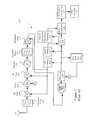
- FIG. 3illustrates a block diagram of a receiver 300 that can automatically change the gains of variable amplifiers during receipt of a packet.
- Receiver 300in general, includes a conventional signal detection block 302 and an early signal detection block 304 .
- Conventional signal detection block 302can include FFT 224 , channel correction circuit 228 , demapping and interleaving circuit 230 , and decoder 232 , which operate as discussed in reference to FIG. 2 .
- antenna 201For context, also illustrated are antenna 201 , RF amplifier 202 , BP filter 204 , mixer 206 , IF amplifier 208 , low pass filters 210 , baseband amplifiers 212 , ADCs 214 , detector 216 , AFC clock recovery circuit 218 , and gain control circuit 220 , each of which also operates as discussed in FIG. 2 .
- signal timing circuit 222as well as channel estimation/pilot phase tracking circuit 226 can be modified to interface with early signal detection block 304 . Therefore, these components have been labeled as signal timing circuit 322 and channel estimation/pilot phase tracking circuit 326 and are shown as being associated with both conventional signal detection block 302 and early signal detection block 304 .
- early signal detection block 304can quickly detect the 3 decoded bits from the SIGNAL symbol that identify the data rate of subsequent data. From these bits, a determination can be made whether the gain setting needs to change based upon the contents of the SIGNAL symbol. If so, then early signal detection block 304 can advantageously change the gains of RF amplifier 202 and IF amplifier 208 .
- early signal detection block 304includes signal timing circuit 322 , channel estimation/pilot phase tracking circuit 326 , a discrete Fourier transform (DFT) circuit 350 , a channel correction circuit 352 , a slicing circuit 354 , a decoder lookup table (LUT) 356 , a select gain change circuit 358 , and an amplitude tracking circuit 360 .
- signal timing circuit 322keeps track of the time that has elapsed since the beginning of a signal to determine the appropriate time to trigger DFT circuit 350 to input the SIGNAL symbol. Because the SIGNAL symbol will occur at the same time in every packet, keeping track of the time allows DFT circuit 350 to input the (still modulated) SIGNAL symbol.
- Signal timing circuit 322operates using a short cyclic recognition circuit of conventional design that detects the existence of the short training symbols. When the repetition ends (taking into consideration multi-path echoes and the like), it is assumed that the signal is at the end of the short training sequence. From that point, signal timing circuit 322 waits a period of time corresponding to the long training symbols and the guard intervals that will occur before the SIGNAL symbol is transmitted and then generates a pulse or other signal to DFT circuit 350 indicating that it should begin obtaining samples of the signal corresponding to the SIGNAL symbol. Note that this pulse will also correspond to the pulse applied to FFT 224 for the SIGNAL symbol.
- DFT circuit 350For both DFT circuit 350 and FFT circuit 224 , samples at the end of the guard interval may be used, whereas the last few samples of the symbol may not be used (i.e. if the peak of the impulse response of the aggregate channel response and filter response is not the first tap). This choice of sampling is then preferably used for all symbols, and the delay in time creates a linear phase across the frequencies. Timing is maintained by adjusting a phase slope in frequency (same as a delay in time) within a given range.
- the six DFT outputs of DFT circuit 350are then input to channel correction circuit 352 , which performs channel correction on the six DFT outputs, based upon the channel estimation obtained from the channel estimator within channel estimation and pilot phase tracking circuit 326 .
- Channel correction circuit 352operates by multiplying the six different outputs from DFT circuit 350 with the appropriate inverted channel estimate provided by channel estimation/pilot phase tracking circuit 326 .
- the inverted channel estimateis obtained based upon the training symbols in the OFDM signal. Because the training symbols are transmitted at unity magnitude and zero phase, the effect of the airwaves over which the signal has been transmitted on the magnitude and phase of the training symbols can be determined. This effect can then be inverted and applied to each of the six different outputs from channel correction circuit 352 to obtain six different channel corrected complex numbers representing the outputs.
- each of the six DFT outputsare also normalized using the output from amplitude tracking circuit 360 .
- Amplitude tracking circuit 360determines the magnitude of the largest component (I or Q), and the channel correction circuit complex normalizes each of the six DFT outputs.
- the largest componentis preferably determined based upon the power of the signal on the pilot symbols, or, alternatively, the training symbols, which are each typically transmitted at a unity magnitude and zero phase, as detected during the period corresponding to the reception of the training symbols associated with the packet.
- Each of the six different channel corrected and normalized complex numbersis then sliced to determine if it corresponds to a digital “1” or a digital “0” by slicing circuit 354 .
- the SIGNAL symbolis BPSK modulated (in this example)
- only the signs of the real portions of these six different complex numbersare needed to obtain the decoded SIGNAL symbol.
- determining whether a BPSK encoded bit is positive or negativecan be easily discerned from looking at the sign of the real portion of the complex number. Specifically, if the sign if positive, then that bit is a “0”, and if the sign is negative, then that bit is “1”. Based upon the sign from the real portion of each of these six numbers, which one of the eight possible transmission rates that the remaining data symbols within the packet are transmitted at can be determined. Slicing circuits that perform as described are well known.
- a complex phase correction of the normalized result obtained by channel correction circuit 352can also occur if samples were obtained that include the guard interval and a timing back off parameter was used to determine which of the samples identify the symbol. For example, if 80 samples were taken in the embodiment described above, 16 will represent the guard interval. The timing back off parameter will indicate where within the 80 samples is the first sample that does not correspond to the guard interval, which can be determined using conventional techniques.
- select gain change circuit 358can determine what the appropriate gain for that data rate should be. In a preferred embodiment of the invention, approximately half of the short training symbols are used to initially adjust the gain based upon the channel conditions for the BPSK symbol. The present invention uses the already determined gain and modifies it based upon the determined data rate/modulation type.
- receiver 300will be inputting data corresponding to the guard interval between the SIGNAL symbol and the first data symbol.
- the automatic gain control amplifiershould preferably still have its gain changed during a guard interval. Accordingly, this is illustrated in FIG. 3 by the signal line from the symbol timing circuit 322 to select gain change circuit 258 , which will transmit an appropriate pulse aligned with the beginning of a guard interval indicating that the gain should be changed at that time. More generally, for any modulation type being used, any period during which redundant information is being sent may be used for changing the gain because the receiver may be unable to process signals correctly for a short time while changing gain.
- the 802.11a standarddefines communication in the 5 GHz band using data rates of 6, 12, 18, 24, 36, and 54 Mbps.
- the 802.11b standarddefines communication in the 2.4 GHz band using data rates of 1, 2, 5.5, and 11 Mbps.
- a recent proposed addition to the 802.11 standards, called the 802.11g standarduses the high data rates of 802.11a in the frequency band of 802.11b, i.e. 2.4 GHz.
- the 802.11g standardincorporates the modulation types from both the 802.11a and 802.11b standards (wherein the 802.11b standard uses CCK modulation and the 802.11a standard uses OFDM modulation).
- CCK packetstypically have lower requirements for SNR, but may require more blocker tolerance than OFDM packets.
- XR packetsmay require even less SNR, but may require even more blocker tolerance than CCK packets. Due to the format differences between CCK, XR, and OFDM packets, the variable gain modifications can be made at different times. In accordance with one aspect of the invention, a first variable gain modification can be made after the modulation type is identified and a second variable gain modification can be made after the modulation rate is identified. These modifications will be further described in reference to FIGS. 4A , 4 B, 5 , and 6 .
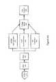
- FIG. 4Aillustrates components that can be added to receiver 300 to identify the modulation type of the received signal.
- a finite impulse response (FIR 1 ) filter 401can be used to provide a down sample of 2 to the output signals of ADCs 314 (typically only used in 802.11a mode).
- Another FIR (i.e. FIR 2 ) filter 402can be used to filter out any nearby blocking signals.
- the output signal of filter 402can be provided to three correlators: an OFDM self-correlator 403 , a CCK cross-correlator 404 , and an XR cross-correlator 405 .
- each of correlators 403 , 404 , and 405compares the output signal of filter 402 to a unique characteristic associated with its modulation type.
- characteristiccan refer to any number of identifying means including, for example, patterns and/or periodicity of a given period.
- Barker signals(an 11-chip spreading code) are multiplied by either ⁇ 1 or +1.
- FIG. 4Billustrates a short CCK format, in contrast to a long CCK format (as defined by the 2001 draft supplement to the IEEE 802.11b standard).
- the ⁇ 1/+1 multiplicationis applied in a similar manner, thereby establishing a CCK pattern.
- the term “cross-correlator”is appropriate in CCK.
- 15 symbols(called mediums) of duration 1.6 us at the base rate (32 samples at Nyquist rate) are provided. These mediums are combined with a secondary PN codes, such that each medium has a predetermined sign (i.e. +/ ⁇ ).
- Preamble detectionoperates by cross-correlating the input signal with a single medium, then self-correlating this output over a gap of the duration of a medium. Therefore, an XR signal can have both self- and cross-correlation aspects.
- the XR signalis a proprietary OFDM-based modulation available through Atheros Communications, Inc.
- XR signalshave a lower bit rate than OFDM signals and therefore have even greater blocker tolerances.
- Each of correlators 403 , 404 , and 405provides a correlation value to a voting block 406 based on the unique characteristics associated with its modulation type.
- a correlation valueindicates the likelihood that the signal output by filter 402 is of a certain modulation type.
- voting block 406determines the highest of the three correlation values, thereby designating the most probable modulation type. At this point, voting block 406 can provide this designation to gain control circuit 220 , which in turn can modify the gains of RF amplifier 202 and IF amplifier 208 (shown in FIG. 3 ).
- DFT 350can operate using the same processes described for the OFDM SIGNAL.
- the modulation typecan also be advantageously used to modify the gains of RF amplifier 202 and IF amplifier 208 .
- the gain of baseband amplifiers 212can also be modified by early signal detection block 304 (as indicated by the dotted line).
- the gains of RF amplifier 202 , IF amplifier 208 , and baseband amplifiers 212can be modified earlier than waiting for subsequent portions of the modulated signal. These variable gains could be further modified after the modulation rate is identified.
- modification of the variable amplifierscould be performed after complete analysis by early signal detect circuit 304 .
- the appropriate gain modificationscould be made based on multiple portions of the modulated signal.
- This embodimentcan be used effectively in modulated signals having a very short preamble (e.g. an OFDM signal).
- FIG. 5illustrates an exemplary process 500 that can be used to modify variable gains at multiple times during the receipt of a modulated signal.
- an initial gaincan be set in step 501 .
- this initial gainis a lower gain to accommodate large potential blockers.
- the modulation typecan be determined using unique characteristics associated with the modulated signal.
- this modulation typecan be used to modify any variable amplifier gains, e.g. RF, IF, and/or baseband amplifiers, in step 503 .
- the modulation ratecan be determined in step 504 .
- the variable amplifier gainscan be further modified based on the modulation rate in step 505 . Of importance, at either step 503 or step 505 , the gain can be increased to result in a higher SNR and a lower blocker tolerance.
- step 502a modulation type is identified in step 502 and a corresponding gain modification is made in step 503 .
- additional steps to adjust the variable gainmay be unnecessary.
- the variable gainsshould provide the same blocker tolerance, as the 802.11b specification requires the same blocker tolerance for all rates.
- an OFDM or XR modulation typeis identified, then multiple variable gain modifications based on data rate could still be beneficial. For example, eight different blocker tolerances can be applied to OFDM signals depending on the data rate.
- the vote designation generated by voting block 406can also be provided to other components to facilitate optimal processing of the received signals.
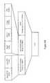
- FIG. 6illustrates a processing block 600 that can be provided in a receiver.
- ADCs 314 , filters 401 and 402 , as well as FFT 224are shown.
- a multiplexer 604receives inputs from a Turbo line 602 , filter 401 , and an interpolator 603 .
- Multiplexer 604can be controlled by the output generated by voting block 406 and a turbo mode register 607 .
- a root-raised cosine (RRC) FIR filter 601can be used when a CCK modulation type is identified, the received data rate is identified to be 44 MHz, and the desired data rate is identified to be 22 MHz. Filter 601 ensures that the subsequent data symbols are correctly converted from 44 MHz to the desired 22 MHz and then provided to a CCK decoder block 605 (note that if a CCK signal is identified in voting, then CCK decoder block 605 is activated, otherwise it is turned off for the duration of the packet).
- Turbo signal line 602can be selected (by a signal from a turbo mode register 607 ) when an OFDM modulation type is identified and the data rate received and desired is 80 MHz (i.e.
- Filter 401can be selected when an OFDM modulation type is identified, the received data rate is identified to be 80, and the desired data rate is identified to be 40 MHz.
- Interpolator 603can be selected when an OFDM modulation type is identified, the received data rate is identified to be 44, and the desired data rate is identified to be 40 MHz.
- An exemplary interpolator 603is described in U.S. patent application Ser. No. 10/367,527, entitled “Receiving and Transmitting Signals Having Multiple Modulation Types Using Sequencing Interpolator”, filed on Feb. 14, 2003 by Atheros Communications, Inc., which is incorporated by reference herein.
- the processed signals selected by multiplexer 604can then be provided to both filter 402 as well as rotator 606 .
- rotator 606adjusts the frequency offset and essentially replaces detector 216 and AFC clock recovery circuit 218 ( FIG. 3 ).
- Rotator 606provides its output to FFT 224 , which along with the other components in receiver 300 , operate to accurately reconstruct the received signals.
Landscapes
- Engineering & Computer Science (AREA)
- Computer Networks & Wireless Communication (AREA)
- Signal Processing (AREA)
- Artificial Intelligence (AREA)
- Circuits Of Receivers In General (AREA)
Abstract
Description
| TABLE 1 | |
| 0 | 6 |
| 1 | 9 |
| 2 | 12 Mb |
| 3 | 18 Mb |
| 4 | 24 Mb |
| 5 | 36 Mb |
| 6 | 48 Mb |
| 7 | 54 Mb |
| TABLE 2 | |||||
| 000000: 4 | 010000: 2 | 100000: 2 | 110000: 2 | ||
| 000001: 0 | 010001: 3 | 100001: 3 | 110001: 3* | ||
| 000010: 1 | 010010: 2 | 100010: 2 | 110010: 2* | ||
| 000011: 5 | 010011: 2 | 100011: 2 | 110011: 2 | ||
| 000100: 0 | 010100: 0 | 100100: 0 | 110100: 7 | ||
| 000101: 0* | 010101: 0 | 100101: 0 | 110101: 3 | ||
| 000110: 1* | 010110: 1 | 100110: 1 | 110110: 2 | ||
| 000111: 0 | 010111: 0 | 100111: 0 | 110111: 6 | ||
| 001000: 4* | 011000: 4 | 101000: 4 | 111000: 7 | ||
| 001001: 4 | 011001: 3 | 101001: 3 | 111001: 3 | ||
| 001010: 4 | 011010: 2 | 101010: 2 | 111010: 2 | ||
| 001011: 5* | 011011: 5 | 101011: 5 | 111011: 6 | ||
| 001100: 4 | 011100: 7 | 101100: 7 | 111100: 7* | ||
| 001101: 0 | 011101: 0 | 101101: 0 | 111101: 6 | ||
| 001110: 1 | 011110: 1 | 101110: 1 | 111110: 6 | ||
| 001111: 5 | 011111: 6 | 101111: 6 | 111111: 6* | ||
The table values are a function of the convolutional encoder used in the IEEE 802.11a standard and the eight values that correspond to the eight ideal rates within an 802.11a system are identified with an asterisk (*). If a different signal having a different error encoding is used, a corresponding maximum likelihood decoder table based upon the error encoding used can easily be constructed.
Claims (20)
Priority Applications (1)
| Application Number | Priority Date | Filing Date | Title |
|---|---|---|---|
| US10/367,049US8498368B1 (en) | 2001-04-11 | 2003-02-14 | Method and system for optimizing gain changes by identifying modulation type and rate |
Applications Claiming Priority (2)
| Application Number | Priority Date | Filing Date | Title |
|---|---|---|---|
| US09/833,749US7027530B2 (en) | 2001-04-11 | 2001-04-11 | Method and apparatus for maximizing receiver performance utilizing mid-packet gain changes |
| US10/367,049US8498368B1 (en) | 2001-04-11 | 2003-02-14 | Method and system for optimizing gain changes by identifying modulation type and rate |
Related Parent Applications (1)
| Application Number | Title | Priority Date | Filing Date |
|---|---|---|---|
| US09/833,749Continuation-In-PartUS7027530B2 (en) | 2001-04-11 | 2001-04-11 | Method and apparatus for maximizing receiver performance utilizing mid-packet gain changes |
Publications (1)
| Publication Number | Publication Date |
|---|---|
| US8498368B1true US8498368B1 (en) | 2013-07-30 |
Family
ID=48808707
Family Applications (1)
| Application Number | Title | Priority Date | Filing Date |
|---|---|---|---|
| US10/367,049Expired - Fee RelatedUS8498368B1 (en) | 2001-04-11 | 2003-02-14 | Method and system for optimizing gain changes by identifying modulation type and rate |
Country Status (1)
| Country | Link |
|---|---|
| US (1) | US8498368B1 (en) |
Cited By (60)
| Publication number | Priority date | Publication date | Assignee | Title |
|---|---|---|---|---|
| US20150358024A1 (en)* | 2014-06-09 | 2015-12-10 | Samsung Electronics Co., Ltd. | Clock data recovery circuit and a method of operating the same |
| US9419564B2 (en) | 2014-05-16 | 2016-08-16 | Kandou Labs, S.A. | Symmetric linear equalization circuit with increased gain |
| US9419828B2 (en) | 2013-11-22 | 2016-08-16 | Kandou Labs, S.A. | Multiwire linear equalizer for vector signaling code receiver |
| US9424908B2 (en) | 2010-12-30 | 2016-08-23 | Kandou Labs, S.A. | Differential vector storage for dynamic random access memory |
| US9432082B2 (en) | 2014-07-17 | 2016-08-30 | Kandou Labs, S.A. | Bus reversable orthogonal differential vector signaling codes |
| US9444654B2 (en) | 2014-07-21 | 2016-09-13 | Kandou Labs, S.A. | Multidrop data transfer |
| US9450791B2 (en) | 2010-05-20 | 2016-09-20 | Kandoub Lab, S.A. | Circuits for efficient detection of vector signaling codes for chip-to-chip communication |
| US9450744B2 (en) | 2010-05-20 | 2016-09-20 | Kandou Lab, S.A. | Control loop management and vector signaling code communications links |
| US9461862B2 (en) | 2014-08-01 | 2016-10-04 | Kandou Labs, S.A. | Orthogonal differential vector signaling codes with embedded clock |
| US9479369B1 (en) | 2010-05-20 | 2016-10-25 | Kandou Labs, S.A. | Vector signaling codes with high pin-efficiency for chip-to-chip communication and storage |
| US9485057B2 (en) | 2010-05-20 | 2016-11-01 | Kandou Labs, S.A. | Vector signaling with reduced receiver complexity |
| US9509437B2 (en) | 2014-05-13 | 2016-11-29 | Kandou Labs, S.A. | Vector signaling code with improved noise margin |
| US9524106B1 (en) | 2012-05-14 | 2016-12-20 | Kandou Labs, S.A. | Storage method and apparatus for random access memory using codeword storage |
| US9544015B2 (en) | 2014-06-25 | 2017-01-10 | Kandou Labs, S.A. | Multilevel driver for high speed chip-to-chip communications |
| US9557760B1 (en) | 2015-10-28 | 2017-01-31 | Kandou Labs, S.A. | Enhanced phase interpolation circuit |
| US9564994B2 (en) | 2010-05-20 | 2017-02-07 | Kandou Labs, S.A. | Fault tolerant chip-to-chip communication with advanced voltage |
| US9577815B1 (en) | 2015-10-29 | 2017-02-21 | Kandou Labs, S.A. | Clock data alignment system for vector signaling code communications link |
| US9577664B2 (en) | 2010-05-20 | 2017-02-21 | Kandou Labs, S.A. | Efficient processing and detection of balanced codes |
| US9596109B2 (en) | 2010-05-20 | 2017-03-14 | Kandou Labs, S.A. | Methods and systems for high bandwidth communications interface |
| US9607673B1 (en)* | 2010-05-20 | 2017-03-28 | Kandou Labs S.A. | Methods and systems for pin-efficient memory controller interface using vector signaling codes for chip-to-chip communication |
| US9667379B2 (en) | 2010-06-04 | 2017-05-30 | Ecole Polytechnique Federale De Lausanne (Epfl) | Error control coding for orthogonal differential vector signaling |
| US9674014B2 (en) | 2014-10-22 | 2017-06-06 | Kandou Labs, S.A. | Method and apparatus for high speed chip-to-chip communications |
| US9686107B2 (en) | 2010-05-20 | 2017-06-20 | Kandou Labs, S.A. | Methods and systems for chip-to-chip communication with reduced simultaneous switching noise |
| US9686106B2 (en) | 2014-02-28 | 2017-06-20 | Kandou Labs, S.A. | Clock-embedded vector signaling codes |
| US9806761B1 (en) | 2014-01-31 | 2017-10-31 | Kandou Labs, S.A. | Methods and systems for reduction of nearest-neighbor crosstalk |
| US9825723B2 (en) | 2010-05-20 | 2017-11-21 | Kandou Labs, S.A. | Methods and systems for skew tolerance in and advanced detectors for vector signaling codes for chip-to-chip communication |
| US9825677B2 (en) | 2010-04-30 | 2017-11-21 | ECOLE POLYTECHNIQUE FéDéRALE DE LAUSANNE | Orthogonal differential vector signaling |
| US9832046B2 (en) | 2015-06-26 | 2017-11-28 | Kandou Labs, S.A. | High speed communications system |
| US9838017B2 (en) | 2010-05-20 | 2017-12-05 | Kandou Labs, S.A. | Methods and systems for high bandwidth chip-to-chip communcations interface |
| US9852806B2 (en) | 2014-06-20 | 2017-12-26 | Kandou Labs, S.A. | System for generating a test pattern to detect and isolate stuck faults for an interface using transition coding |
| US9900186B2 (en) | 2014-07-10 | 2018-02-20 | Kandou Labs, S.A. | Vector signaling codes with increased signal to noise characteristics |
| US9906358B1 (en) | 2016-08-31 | 2018-02-27 | Kandou Labs, S.A. | Lock detector for phase lock loop |
| US9985745B2 (en) | 2013-06-25 | 2018-05-29 | Kandou Labs, S.A. | Vector signaling with reduced receiver complexity |
| US9985634B2 (en) | 2010-05-20 | 2018-05-29 | Kandou Labs, S.A. | Data-driven voltage regulator |
| US10003454B2 (en) | 2016-04-22 | 2018-06-19 | Kandou Labs, S.A. | Sampler with low input kickback |
| US10003315B2 (en) | 2016-01-25 | 2018-06-19 | Kandou Labs S.A. | Voltage sampler driver with enhanced high-frequency gain |
| US20180198584A1 (en)* | 2017-01-09 | 2018-07-12 | Qualcomm Incorporated | Using sequences of pilot repetitions for receiver adaptation |
| US10056903B2 (en) | 2016-04-28 | 2018-08-21 | Kandou Labs, S.A. | Low power multilevel driver |
| US10055372B2 (en) | 2015-11-25 | 2018-08-21 | Kandou Labs, S.A. | Orthogonal differential vector signaling codes with embedded clock |
| US10057049B2 (en) | 2016-04-22 | 2018-08-21 | Kandou Labs, S.A. | High performance phase locked loop |
| US10091035B2 (en) | 2013-04-16 | 2018-10-02 | Kandou Labs, S.A. | Methods and systems for high bandwidth communications interface |
| US10116468B1 (en) | 2017-06-28 | 2018-10-30 | Kandou Labs, S.A. | Low power chip-to-chip bidirectional communications |
| US10153591B2 (en) | 2016-04-28 | 2018-12-11 | Kandou Labs, S.A. | Skew-resistant multi-wire channel |
| US10200188B2 (en) | 2016-10-21 | 2019-02-05 | Kandou Labs, S.A. | Quadrature and duty cycle error correction in matrix phase lock loop |
| US10200218B2 (en) | 2016-10-24 | 2019-02-05 | Kandou Labs, S.A. | Multi-stage sampler with increased gain |
| US10203226B1 (en) | 2017-08-11 | 2019-02-12 | Kandou Labs, S.A. | Phase interpolation circuit |
| US10277431B2 (en) | 2016-09-16 | 2019-04-30 | Kandou Labs, S.A. | Phase rotation circuit for eye scope measurements |
| US10326623B1 (en) | 2017-12-08 | 2019-06-18 | Kandou Labs, S.A. | Methods and systems for providing multi-stage distributed decision feedback equalization |
| US10333741B2 (en) | 2016-04-28 | 2019-06-25 | Kandou Labs, S.A. | Vector signaling codes for densely-routed wire groups |
| US10348436B2 (en) | 2014-02-02 | 2019-07-09 | Kandou Labs, S.A. | Method and apparatus for low power chip-to-chip communications with constrained ISI ratio |
| US10372665B2 (en) | 2016-10-24 | 2019-08-06 | Kandou Labs, S.A. | Multiphase data receiver with distributed DFE |
| US10467177B2 (en) | 2017-12-08 | 2019-11-05 | Kandou Labs, S.A. | High speed memory interface |
| US10554380B2 (en) | 2018-01-26 | 2020-02-04 | Kandou Labs, S.A. | Dynamically weighted exclusive or gate having weighted output segments for phase detection and phase interpolation |
| US10666297B2 (en) | 2017-04-14 | 2020-05-26 | Kandou Labs, S.A. | Pipelined forward error correction for vector signaling code channel |
| US10686583B2 (en) | 2017-07-04 | 2020-06-16 | Kandou Labs, S.A. | Method for measuring and correcting multi-wire skew |
| US10693473B2 (en) | 2017-05-22 | 2020-06-23 | Kandou Labs, S.A. | Multi-modal data-driven clock recovery circuit |
| US10693688B2 (en) | 2017-12-28 | 2020-06-23 | Kandou Labs, S.A. | Synchronously-switched multi-input demodulating comparator |
| US10693587B2 (en) | 2017-07-10 | 2020-06-23 | Kandou Labs, S.A. | Multi-wire permuted forward error correction |
| US11240076B2 (en) | 2014-05-13 | 2022-02-01 | Kandou Labs, S.A. | Vector signaling code with improved noise margin |
| US11831472B1 (en) | 2022-08-30 | 2023-11-28 | Kandou Labs SA | Pre-scaler for orthogonal differential vector signalling |
Citations (20)
| Publication number | Priority date | Publication date | Assignee | Title |
|---|---|---|---|---|
| US5519548A (en)* | 1993-03-31 | 1996-05-21 | Hewlett-Packard Company | Using read channel noise to initialize read channel for head position calibration in a magnetic data storage device |
| US5812523A (en) | 1995-03-01 | 1998-09-22 | Telia Ab | Method and device for synchronization at OFDM-system |
| WO1999021287A1 (en) | 1997-10-20 | 1999-04-29 | Comsat Corporation | Adaptive modulation technique and satellite communication network implementing the same |
| US6002723A (en)* | 1997-08-15 | 1999-12-14 | Lockheed Martin Corporation | Digital receiver having programmable complex threshold detectors and threshold interpreters |
| US6009129A (en) | 1997-02-28 | 1999-12-28 | Nokia Mobile Phones | Device and method for detection and reduction of intermodulation distortion |
| US6188717B1 (en) | 1996-11-19 | 2001-02-13 | Deutsche Forschungsanstalt Fur Luft-Und Raumfahrt E.V. | Method of simultaneous radio transmission of digital data between a plurality of subscriber stations and a base station |
| US6192070B1 (en) | 1998-01-02 | 2001-02-20 | Mitsubishi Electric Research Laboratories, Inc. | Universal modem for digital video, audio and data communications |
| US6246698B1 (en)* | 1996-06-19 | 2001-06-12 | Digital Radio Express, Inc. | In-band on-channel digital broadcasting method and system |
| US6392570B1 (en) | 2000-05-08 | 2002-05-21 | Crossroads Systems, Inc. | Method and system for decoding 8-bit/10-bit data using limited width decoders |
| US6400928B1 (en)* | 1999-11-19 | 2002-06-04 | Telefonaktiebolaget L M Ericsson (Publ) | Method and system for blind detection of modulation |
| US20020094050A1 (en) | 2000-03-15 | 2002-07-18 | Takashi Usui | Data modulation method, data modulation device and communication device |
| US6456670B1 (en) | 1998-01-22 | 2002-09-24 | Infineon Technologies Ag | Method for processing a signal containing data symbols |
| US6505037B1 (en)* | 1999-06-29 | 2003-01-07 | Sharp Laboratories Of America, Inc. | Data unit detection including antenna diversity |
| US6549561B2 (en) | 2001-02-21 | 2003-04-15 | Magis Networks, Inc. | OFDM pilot tone tracking for wireless LAN |
| US6711221B1 (en) | 2000-02-16 | 2004-03-23 | Thomson Licensing S.A. | Sampling offset correction in an orthogonal frequency division multiplexing system |
| US6735423B1 (en)* | 1999-05-18 | 2004-05-11 | General Instrument Corporation | Method and apparatus for obtaining optimal performance in a receiver |
| US6747569B2 (en)* | 2001-02-02 | 2004-06-08 | Dbi Corporation | Downhole telemetry and control system |
| US6850493B1 (en)* | 1998-03-09 | 2005-02-01 | Broadcom Corporation | Off-line broadband network interface |
| US6882679B2 (en)* | 2000-12-29 | 2005-04-19 | Sharp Laboratories Of America, Inc. | Extension of wireless local area network communication system to accommodate higher data rates while preserving legacy receiver features |
| US7027530B2 (en) | 2001-04-11 | 2006-04-11 | Atheros Communications, Inc. | Method and apparatus for maximizing receiver performance utilizing mid-packet gain changes |
- 2003
- 2003-02-14USUS10/367,049patent/US8498368B1/ennot_activeExpired - Fee Related
Patent Citations (20)
| Publication number | Priority date | Publication date | Assignee | Title |
|---|---|---|---|---|
| US5519548A (en)* | 1993-03-31 | 1996-05-21 | Hewlett-Packard Company | Using read channel noise to initialize read channel for head position calibration in a magnetic data storage device |
| US5812523A (en) | 1995-03-01 | 1998-09-22 | Telia Ab | Method and device for synchronization at OFDM-system |
| US6246698B1 (en)* | 1996-06-19 | 2001-06-12 | Digital Radio Express, Inc. | In-band on-channel digital broadcasting method and system |
| US6188717B1 (en) | 1996-11-19 | 2001-02-13 | Deutsche Forschungsanstalt Fur Luft-Und Raumfahrt E.V. | Method of simultaneous radio transmission of digital data between a plurality of subscriber stations and a base station |
| US6009129A (en) | 1997-02-28 | 1999-12-28 | Nokia Mobile Phones | Device and method for detection and reduction of intermodulation distortion |
| US6002723A (en)* | 1997-08-15 | 1999-12-14 | Lockheed Martin Corporation | Digital receiver having programmable complex threshold detectors and threshold interpreters |
| WO1999021287A1 (en) | 1997-10-20 | 1999-04-29 | Comsat Corporation | Adaptive modulation technique and satellite communication network implementing the same |
| US6192070B1 (en) | 1998-01-02 | 2001-02-20 | Mitsubishi Electric Research Laboratories, Inc. | Universal modem for digital video, audio and data communications |
| US6456670B1 (en) | 1998-01-22 | 2002-09-24 | Infineon Technologies Ag | Method for processing a signal containing data symbols |
| US6850493B1 (en)* | 1998-03-09 | 2005-02-01 | Broadcom Corporation | Off-line broadband network interface |
| US6735423B1 (en)* | 1999-05-18 | 2004-05-11 | General Instrument Corporation | Method and apparatus for obtaining optimal performance in a receiver |
| US6505037B1 (en)* | 1999-06-29 | 2003-01-07 | Sharp Laboratories Of America, Inc. | Data unit detection including antenna diversity |
| US6400928B1 (en)* | 1999-11-19 | 2002-06-04 | Telefonaktiebolaget L M Ericsson (Publ) | Method and system for blind detection of modulation |
| US6711221B1 (en) | 2000-02-16 | 2004-03-23 | Thomson Licensing S.A. | Sampling offset correction in an orthogonal frequency division multiplexing system |
| US20020094050A1 (en) | 2000-03-15 | 2002-07-18 | Takashi Usui | Data modulation method, data modulation device and communication device |
| US6392570B1 (en) | 2000-05-08 | 2002-05-21 | Crossroads Systems, Inc. | Method and system for decoding 8-bit/10-bit data using limited width decoders |
| US6882679B2 (en)* | 2000-12-29 | 2005-04-19 | Sharp Laboratories Of America, Inc. | Extension of wireless local area network communication system to accommodate higher data rates while preserving legacy receiver features |
| US6747569B2 (en)* | 2001-02-02 | 2004-06-08 | Dbi Corporation | Downhole telemetry and control system |
| US6549561B2 (en) | 2001-02-21 | 2003-04-15 | Magis Networks, Inc. | OFDM pilot tone tracking for wireless LAN |
| US7027530B2 (en) | 2001-04-11 | 2006-04-11 | Atheros Communications, Inc. | Method and apparatus for maximizing receiver performance utilizing mid-packet gain changes |
Non-Patent Citations (1)
| Title |
|---|
| International Search Report-PCT/US2002/011214, ISA/US, Aug. 7, 2002. |
Cited By (119)
| Publication number | Priority date | Publication date | Assignee | Title |
|---|---|---|---|---|
| US11611377B2 (en) | 2010-04-30 | 2023-03-21 | Ecole Polytechnique Federale De Lausanne | Orthogonal differential vector signaling |
| US10355756B2 (en) | 2010-04-30 | 2019-07-16 | ECOLE POLYTECHNIQUE FéDéRALE DE LAUSANNE | Orthogonal differential vector signaling |
| US9825677B2 (en) | 2010-04-30 | 2017-11-21 | ECOLE POLYTECHNIQUE FéDéRALE DE LAUSANNE | Orthogonal differential vector signaling |
| US10985806B2 (en) | 2010-04-30 | 2021-04-20 | ECOLE POLYTECHNIQUE FéDéRALE DE LAUSANNE | Orthogonal differential vector signaling |
| US9479369B1 (en) | 2010-05-20 | 2016-10-25 | Kandou Labs, S.A. | Vector signaling codes with high pin-efficiency for chip-to-chip communication and storage |
| US9929818B2 (en) | 2010-05-20 | 2018-03-27 | Kandou Bus, S.A. | Methods and systems for selection of unions of vector signaling codes for power and pin efficient chip-to-chip communication |
| US9838017B2 (en) | 2010-05-20 | 2017-12-05 | Kandou Labs, S.A. | Methods and systems for high bandwidth chip-to-chip communcations interface |
| US9450791B2 (en) | 2010-05-20 | 2016-09-20 | Kandoub Lab, S.A. | Circuits for efficient detection of vector signaling codes for chip-to-chip communication |
| US9450744B2 (en) | 2010-05-20 | 2016-09-20 | Kandou Lab, S.A. | Control loop management and vector signaling code communications links |
| US10468078B2 (en) | 2010-05-20 | 2019-11-05 | Kandou Labs, S.A. | Methods and systems for pin-efficient memory controller interface using vector signaling codes for chip-to-chip communication |
| US9819522B2 (en) | 2010-05-20 | 2017-11-14 | Kandou Labs, S.A. | Circuits for efficient detection of vector signaling codes for chip-to-chip communication |
| US9485057B2 (en) | 2010-05-20 | 2016-11-01 | Kandou Labs, S.A. | Vector signaling with reduced receiver complexity |
| US9825723B2 (en) | 2010-05-20 | 2017-11-21 | Kandou Labs, S.A. | Methods and systems for skew tolerance in and advanced detectors for vector signaling codes for chip-to-chip communication |
| US9692555B2 (en) | 2010-05-20 | 2017-06-27 | Kandou Labs, S.A. | Vector signaling with reduced receiver complexity |
| US9686107B2 (en) | 2010-05-20 | 2017-06-20 | Kandou Labs, S.A. | Methods and systems for chip-to-chip communication with reduced simultaneous switching noise |
| US9985634B2 (en) | 2010-05-20 | 2018-05-29 | Kandou Labs, S.A. | Data-driven voltage regulator |
| US9564994B2 (en) | 2010-05-20 | 2017-02-07 | Kandou Labs, S.A. | Fault tolerant chip-to-chip communication with advanced voltage |
| US10044452B2 (en) | 2010-05-20 | 2018-08-07 | Kandou Labs, S.A. | Methods and systems for skew tolerance in and advanced detectors for vector signaling codes for chip-to-chip communication |
| US9577664B2 (en) | 2010-05-20 | 2017-02-21 | Kandou Labs, S.A. | Efficient processing and detection of balanced codes |
| US9596109B2 (en) | 2010-05-20 | 2017-03-14 | Kandou Labs, S.A. | Methods and systems for high bandwidth communications interface |
| US9607673B1 (en)* | 2010-05-20 | 2017-03-28 | Kandou Labs S.A. | Methods and systems for pin-efficient memory controller interface using vector signaling codes for chip-to-chip communication |
| US9667379B2 (en) | 2010-06-04 | 2017-05-30 | Ecole Polytechnique Federale De Lausanne (Epfl) | Error control coding for orthogonal differential vector signaling |
| US10164809B2 (en) | 2010-12-30 | 2018-12-25 | Kandou Labs, S.A. | Circuits for efficient detection of vector signaling codes for chip-to-chip communication |
| US9424908B2 (en) | 2010-12-30 | 2016-08-23 | Kandou Labs, S.A. | Differential vector storage for dynamic random access memory |
| US9524106B1 (en) | 2012-05-14 | 2016-12-20 | Kandou Labs, S.A. | Storage method and apparatus for random access memory using codeword storage |
| US10091035B2 (en) | 2013-04-16 | 2018-10-02 | Kandou Labs, S.A. | Methods and systems for high bandwidth communications interface |
| US11374801B2 (en) | 2013-04-16 | 2022-06-28 | Kandou Labs, S.A. | Methods and systems for high bandwidth communications interface |
| US12206531B2 (en) | 2013-04-16 | 2025-01-21 | Kandou Labs, S.A. | Methods and systems for high bandwidth communications interface |
| US9985745B2 (en) | 2013-06-25 | 2018-05-29 | Kandou Labs, S.A. | Vector signaling with reduced receiver complexity |
| US9419828B2 (en) | 2013-11-22 | 2016-08-16 | Kandou Labs, S.A. | Multiwire linear equalizer for vector signaling code receiver |
| US10177812B2 (en) | 2014-01-31 | 2019-01-08 | Kandou Labs, S.A. | Methods and systems for reduction of nearest-neighbor crosstalk |
| US9806761B1 (en) | 2014-01-31 | 2017-10-31 | Kandou Labs, S.A. | Methods and systems for reduction of nearest-neighbor crosstalk |
| US10348436B2 (en) | 2014-02-02 | 2019-07-09 | Kandou Labs, S.A. | Method and apparatus for low power chip-to-chip communications with constrained ISI ratio |
| US11683113B2 (en) | 2014-02-02 | 2023-06-20 | Kandou Labs, S.A. | Method and apparatus for low power chip-to-chip communications with constrained ISI ratio |
| US11025359B2 (en) | 2014-02-02 | 2021-06-01 | Kandou Labs, S.A. | Method and apparatus for low power chip-to-chip communications with constrained ISI ratio |
| US12136996B2 (en) | 2014-02-02 | 2024-11-05 | Kandou Labs, S.A. | Method and apparatus for low power chip-to-chip communications with constrained ISI ratio |
| US9686106B2 (en) | 2014-02-28 | 2017-06-20 | Kandou Labs, S.A. | Clock-embedded vector signaling codes |
| US10020966B2 (en) | 2014-02-28 | 2018-07-10 | Kandou Labs, S.A. | Vector signaling codes with high pin-efficiency for chip-to-chip communication and storage |
| US10374846B2 (en) | 2014-02-28 | 2019-08-06 | Kandou Labs, S.A. | Clock-embedded vector signaling codes |
| US10805129B2 (en) | 2014-02-28 | 2020-10-13 | Kandou Labs, S.A. | Clock-embedded vector signaling codes |
| US12057976B2 (en) | 2014-05-13 | 2024-08-06 | Kandou Labs, S.A. | Vector signaling code with improved noise margin |
| US11240076B2 (en) | 2014-05-13 | 2022-02-01 | Kandou Labs, S.A. | Vector signaling code with improved noise margin |
| US10333749B2 (en) | 2014-05-13 | 2019-06-25 | Kandou Labs, S.A. | Vector signaling code with improved noise margin |
| US9509437B2 (en) | 2014-05-13 | 2016-11-29 | Kandou Labs, S.A. | Vector signaling code with improved noise margin |
| US11716227B2 (en) | 2014-05-13 | 2023-08-01 | Kandou Labs, S.A. | Vector signaling code with improved noise margin |
| US9692381B2 (en) | 2014-05-16 | 2017-06-27 | Kandou Labs, S.A. | Symmetric linear equalization circuit with increased gain |
| US9419564B2 (en) | 2014-05-16 | 2016-08-16 | Kandou Labs, S.A. | Symmetric linear equalization circuit with increased gain |
| US9432028B2 (en)* | 2014-06-09 | 2016-08-30 | Samsung Electronics Co., Ltd. | Clock data recovery circuit and a method of operating the same |
| US20150358024A1 (en)* | 2014-06-09 | 2015-12-10 | Samsung Electronics Co., Ltd. | Clock data recovery circuit and a method of operating the same |
| US9852806B2 (en) | 2014-06-20 | 2017-12-26 | Kandou Labs, S.A. | System for generating a test pattern to detect and isolate stuck faults for an interface using transition coding |
| US9544015B2 (en) | 2014-06-25 | 2017-01-10 | Kandou Labs, S.A. | Multilevel driver for high speed chip-to-chip communications |
| US9917711B2 (en) | 2014-06-25 | 2018-03-13 | Kandou Labs, S.A. | Multilevel driver for high speed chip-to-chip communications |
| US10091033B2 (en) | 2014-06-25 | 2018-10-02 | Kandou Labs, S.A. | Multilevel driver for high speed chip-to-chip communications |
| US10320588B2 (en) | 2014-07-10 | 2019-06-11 | Kandou Labs, S.A. | Vector signaling codes with increased signal to noise characteristics |
| US9900186B2 (en) | 2014-07-10 | 2018-02-20 | Kandou Labs, S.A. | Vector signaling codes with increased signal to noise characteristics |
| US10404394B2 (en) | 2014-07-17 | 2019-09-03 | Kandou Labs, S.A. | Bus reversible orthogonal differential vector signaling codes |
| US9432082B2 (en) | 2014-07-17 | 2016-08-30 | Kandou Labs, S.A. | Bus reversable orthogonal differential vector signaling codes |
| US10003424B2 (en) | 2014-07-17 | 2018-06-19 | Kandou Labs, S.A. | Bus reversible orthogonal differential vector signaling codes |
| US9444654B2 (en) | 2014-07-21 | 2016-09-13 | Kandou Labs, S.A. | Multidrop data transfer |
| US9893911B2 (en) | 2014-07-21 | 2018-02-13 | Kandou Labs, S.A. | Multidrop data transfer |
| US10230549B2 (en) | 2014-07-21 | 2019-03-12 | Kandou Labs, S.A. | Multidrop data transfer |
| US10652067B2 (en) | 2014-08-01 | 2020-05-12 | Kandou Labs, S.A. | Orthogonal differential vector signaling codes with embedded clock |
| US10122561B2 (en) | 2014-08-01 | 2018-11-06 | Kandou Labs, S.A. | Orthogonal differential vector signaling codes with embedded clock |
| US9461862B2 (en) | 2014-08-01 | 2016-10-04 | Kandou Labs, S.A. | Orthogonal differential vector signaling codes with embedded clock |
| US9838234B2 (en) | 2014-08-01 | 2017-12-05 | Kandou Labs, S.A. | Orthogonal differential vector signaling codes with embedded clock |
| US10243765B2 (en) | 2014-10-22 | 2019-03-26 | Kandou Labs, S.A. | Method and apparatus for high speed chip-to-chip communications |
| US9674014B2 (en) | 2014-10-22 | 2017-06-06 | Kandou Labs, S.A. | Method and apparatus for high speed chip-to-chip communications |
| US10116472B2 (en) | 2015-06-26 | 2018-10-30 | Kandou Labs, S.A. | High speed communications system |
| US10608850B2 (en) | 2015-06-26 | 2020-03-31 | Kandou Labs, S.A. | High speed communications system |
| US11863358B2 (en) | 2015-06-26 | 2024-01-02 | Kandou Labs, S.A. | High speed communications system |
| US11483187B2 (en) | 2015-06-26 | 2022-10-25 | Kandou Labs, S.A. | High speed communications system |
| US11115249B2 (en) | 2015-06-26 | 2021-09-07 | Kandou Labs, S.A. | High speed communications system |
| US9832046B2 (en) | 2015-06-26 | 2017-11-28 | Kandou Labs, S.A. | High speed communications system |
| US10819541B2 (en) | 2015-06-26 | 2020-10-27 | Kandou Labs, S.A. | High speed communications system |
| US10382235B2 (en) | 2015-06-26 | 2019-08-13 | Kandou Labs, S.A. | High speed communications system |
| US9557760B1 (en) | 2015-10-28 | 2017-01-31 | Kandou Labs, S.A. | Enhanced phase interpolation circuit |
| US9577815B1 (en) | 2015-10-29 | 2017-02-21 | Kandou Labs, S.A. | Clock data alignment system for vector signaling code communications link |
| US10055372B2 (en) | 2015-11-25 | 2018-08-21 | Kandou Labs, S.A. | Orthogonal differential vector signaling codes with embedded clock |
| US10324876B2 (en) | 2015-11-25 | 2019-06-18 | Kandou Labs, S.A. | Orthogonal differential vector signaling codes with embedded clock |
| US10003315B2 (en) | 2016-01-25 | 2018-06-19 | Kandou Labs S.A. | Voltage sampler driver with enhanced high-frequency gain |
| US10003454B2 (en) | 2016-04-22 | 2018-06-19 | Kandou Labs, S.A. | Sampler with low input kickback |
| US10057049B2 (en) | 2016-04-22 | 2018-08-21 | Kandou Labs, S.A. | High performance phase locked loop |
| US10056903B2 (en) | 2016-04-28 | 2018-08-21 | Kandou Labs, S.A. | Low power multilevel driver |
| US10153591B2 (en) | 2016-04-28 | 2018-12-11 | Kandou Labs, S.A. | Skew-resistant multi-wire channel |
| US10333741B2 (en) | 2016-04-28 | 2019-06-25 | Kandou Labs, S.A. | Vector signaling codes for densely-routed wire groups |
| US9906358B1 (en) | 2016-08-31 | 2018-02-27 | Kandou Labs, S.A. | Lock detector for phase lock loop |
| US10355852B2 (en) | 2016-08-31 | 2019-07-16 | Kandou Labs, S.A. | Lock detector for phase lock loop |
| US10277431B2 (en) | 2016-09-16 | 2019-04-30 | Kandou Labs, S.A. | Phase rotation circuit for eye scope measurements |
| US10200188B2 (en) | 2016-10-21 | 2019-02-05 | Kandou Labs, S.A. | Quadrature and duty cycle error correction in matrix phase lock loop |
| US10372665B2 (en) | 2016-10-24 | 2019-08-06 | Kandou Labs, S.A. | Multiphase data receiver with distributed DFE |
| US10200218B2 (en) | 2016-10-24 | 2019-02-05 | Kandou Labs, S.A. | Multi-stage sampler with increased gain |
| US10727994B2 (en)* | 2017-01-09 | 2020-07-28 | Qualcomm Incorporated | Using sequences of pilot repetitions for receiver adaptation |
| US20180198584A1 (en)* | 2017-01-09 | 2018-07-12 | Qualcomm Incorporated | Using sequences of pilot repetitions for receiver adaptation |
| US11804855B2 (en) | 2017-04-14 | 2023-10-31 | Kandou Labs, S.A. | Pipelined forward error correction for vector signaling code channel |
| US10666297B2 (en) | 2017-04-14 | 2020-05-26 | Kandou Labs, S.A. | Pipelined forward error correction for vector signaling code channel |
| US11336302B2 (en) | 2017-04-14 | 2022-05-17 | Kandou Labs, S.A. | Pipelined forward error correction for vector signaling code channel |
| US11804845B2 (en) | 2017-05-22 | 2023-10-31 | Kandou Labs, S.A. | Multi-modal data-driven clock recovery circuit |
| US11271571B2 (en) | 2017-05-22 | 2022-03-08 | Kandou Labs, S.A. | Multi-modal data-driven clock recovery circuit |
| US10693473B2 (en) | 2017-05-22 | 2020-06-23 | Kandou Labs, S.A. | Multi-modal data-driven clock recovery circuit |
| US11477055B2 (en) | 2017-06-28 | 2022-10-18 | Kandou Labs, S.A. | Low power chip-to-chip bidirectional communications |
| US10116468B1 (en) | 2017-06-28 | 2018-10-30 | Kandou Labs, S.A. | Low power chip-to-chip bidirectional communications |
| US12057973B2 (en) | 2017-06-28 | 2024-08-06 | Kandou Labs, S.A. | Low power chip-to-chip bidirectional communications |
| US10581644B2 (en) | 2017-06-28 | 2020-03-03 | Kandou Labs, S.A. | Low power chip-to-chip bidirectional communications |
| US11032110B2 (en) | 2017-06-28 | 2021-06-08 | Kandou Labs, S.A. | Low power chip-to-chip bidirectional communications |
| US10686583B2 (en) | 2017-07-04 | 2020-06-16 | Kandou Labs, S.A. | Method for measuring and correcting multi-wire skew |
| US11894926B2 (en) | 2017-07-10 | 2024-02-06 | Kandou Labs, S.A. | Interleaved forward error correction over multiple transport channels |
| US12301352B2 (en) | 2017-07-10 | 2025-05-13 | Kando Labs, SA | Multi-wire permuted forward error correction |
| US11368247B2 (en) | 2017-07-10 | 2022-06-21 | Kandou Labs, S.A. | Multi-wire permuted forward error correction |
| US10693587B2 (en) | 2017-07-10 | 2020-06-23 | Kandou Labs, S.A. | Multi-wire permuted forward error correction |
| US10203226B1 (en) | 2017-08-11 | 2019-02-12 | Kandou Labs, S.A. | Phase interpolation circuit |
| US10326623B1 (en) | 2017-12-08 | 2019-06-18 | Kandou Labs, S.A. | Methods and systems for providing multi-stage distributed decision feedback equalization |
| US10467177B2 (en) | 2017-12-08 | 2019-11-05 | Kandou Labs, S.A. | High speed memory interface |
| US11894961B2 (en) | 2017-12-28 | 2024-02-06 | Kandou Labs, S.A. | Synchronously-switched multi-input demodulating comparator |
| US11063799B2 (en) | 2017-12-28 | 2021-07-13 | Kandou Labs, S.A. | Synchronously-switched multi-input demodulating comparator |
| US11469931B2 (en) | 2017-12-28 | 2022-10-11 | Kandou Labs, S.A. | Synchronously-switched multi-input demodulating comparator |
| US10693688B2 (en) | 2017-12-28 | 2020-06-23 | Kandou Labs, S.A. | Synchronously-switched multi-input demodulating comparator |
| US10554380B2 (en) | 2018-01-26 | 2020-02-04 | Kandou Labs, S.A. | Dynamically weighted exclusive or gate having weighted output segments for phase detection and phase interpolation |
| US11831472B1 (en) | 2022-08-30 | 2023-11-28 | Kandou Labs SA | Pre-scaler for orthogonal differential vector signalling |
| US12206527B2 (en) | 2022-08-30 | 2025-01-21 | Kandou Labs, SA | Pre-scaler for orthogonal differential vector signalling |
Similar Documents
| Publication | Publication Date | Title |
|---|---|---|
| US8498368B1 (en) | Method and system for optimizing gain changes by identifying modulation type and rate | |
| US7027530B2 (en) | Method and apparatus for maximizing receiver performance utilizing mid-packet gain changes | |
| KR100922245B1 (en) | Timing control in orthogonal frequency division multiplex systems based on effective signal-to-noise ratio | |
| US7251282B2 (en) | Receiver and method to detect and synchronize with a symbol boundary of an OFDM symbol | |
| US7298692B2 (en) | Radio base station apparatus and communication terminal | |
| US7822156B2 (en) | Channel estimation | |
| US7986736B2 (en) | Ultra wideband baseband chip with intelligent array radio and method of use thereof | |
| US8625684B2 (en) | Apparatus and method for estimating symbol timing offset in a wireless communication system | |
| KR20060054651A (en) | Synchronization Acquisition Apparatus and Method in Mobile Communication System Using Orthogonal Frequency Division Multiplexing | |
| US7386063B1 (en) | Voting block for identifying WLAN signal modulation type | |
| US7471745B2 (en) | Method and apparatus for channel quality metric generation within a packet-based multicarrier modulation communication system | |
| US7286606B2 (en) | System and method for channelization recognition in a wideband communication system | |
| CN1802828A (en) | Receiver for a multi-carrier communication system | |
| US20060050800A1 (en) | Packet detection in time/frequency hopped wireless communication systems | |
| KR100897660B1 (en) | Method, device and receiver for selecting one channel from a plurality of channels for use in receiving transmission data | |
| US7263147B2 (en) | Low bit error rate antenna switch for wireless communications | |
| US7324608B1 (en) | Efficient subcarrier weighting to enhance receiver performance | |
| JP2007243235A (en) | Wireless communication apparatus and wireless communication method, and computer program | |
| US7710858B1 (en) | Apparatus, system, and method for sample timing synchronization in a receiver | |
| KR20050119053A (en) | The system and method for cinr estimation using puncturing pattern in ofdm | |
| EP1424800A2 (en) | Method and apparatus for channel quality metric generation within a packet-based multicarrier modulation communication system | |
| US20080159445A1 (en) | Viterbi-input auto scaling for packet-based system | |
| WO2004109961A2 (en) | Method and apparatus for transceivers in wireless communications using ofdm spread spectrum | |
| HK1120688A (en) | Timing control in orthogonal frequency division multiplex systems based on effective signal-to-noise ratio | |
| US20080165673A1 (en) | System and method for demodulating data in an orthogonal frequency division modulation system |
Legal Events
| Date | Code | Title | Description |
|---|---|---|---|
| AS | Assignment | Owner name:ATHEROS COMMUNICATIONS, INC., CALIFORNIA Free format text:ASSIGNMENT OF ASSIGNORS INTEREST;ASSIGNORS:HUSTED, PAUL J.;MCFARLAND, WILLIAM J.;MENG, TERESA H.;AND OTHERS;REEL/FRAME:013777/0864 Effective date:20030214 | |
| AS | Assignment | Owner name:QUALCOMM ATHEROS, INC., CALIFORNIA Free format text:MERGER;ASSIGNOR:ATHEROS COMMUNICATIONS, INC.;REEL/FRAME:026599/0360 Effective date:20110105 | |
| AS | Assignment | Owner name:QUALCOMM INCORPORATED, CALIFORNIA Free format text:ASSIGNMENT OF ASSIGNORS INTEREST;ASSIGNOR:QUALCOMM ATHEROS, INC.;REEL/FRAME:029328/0052 Effective date:20121022 | |
| STCF | Information on status: patent grant | Free format text:PATENTED CASE | |
| FEPP | Fee payment procedure | Free format text:PAYER NUMBER DE-ASSIGNED (ORIGINAL EVENT CODE: RMPN); ENTITY STATUS OF PATENT OWNER: LARGE ENTITY Free format text:PAYOR NUMBER ASSIGNED (ORIGINAL EVENT CODE: ASPN); ENTITY STATUS OF PATENT OWNER: LARGE ENTITY | |
| FPAY | Fee payment | Year of fee payment:4 | |
| FEPP | Fee payment procedure | Free format text:MAINTENANCE FEE REMINDER MAILED (ORIGINAL EVENT CODE: REM.); ENTITY STATUS OF PATENT OWNER: LARGE ENTITY | |
| LAPS | Lapse for failure to pay maintenance fees | Free format text:PATENT EXPIRED FOR FAILURE TO PAY MAINTENANCE FEES (ORIGINAL EVENT CODE: EXP.); ENTITY STATUS OF PATENT OWNER: LARGE ENTITY | |
| STCH | Information on status: patent discontinuation | Free format text:PATENT EXPIRED DUE TO NONPAYMENT OF MAINTENANCE FEES UNDER 37 CFR 1.362 | |
| FP | Lapsed due to failure to pay maintenance fee | Effective date:20210730 |