US8497705B2 - Phase change device for interconnection of programmable logic device - Google Patents
Phase change device for interconnection of programmable logic deviceDownload PDFInfo
- Publication number
- US8497705B2 US8497705B2US12/942,462US94246210AUS8497705B2US 8497705 B2US8497705 B2US 8497705B2US 94246210 AUS94246210 AUS 94246210AUS 8497705 B2US8497705 B2US 8497705B2
- Authority
- US
- United States
- Prior art keywords
- phase change
- interconnect
- amorphous region
- programming
- logic blocks
- Prior art date
- Legal status (The legal status is an assumption and is not a legal conclusion. Google has not performed a legal analysis and makes no representation as to the accuracy of the status listed.)
- Active
Links
Images


Classifications
- G—PHYSICS
- G11—INFORMATION STORAGE
- G11C—STATIC STORES
- G11C13/00—Digital stores characterised by the use of storage elements not covered by groups G11C11/00, G11C23/00, or G11C25/00
- G11C13/0002—Digital stores characterised by the use of storage elements not covered by groups G11C11/00, G11C23/00, or G11C25/00 using resistive RAM [RRAM] elements
- G11C13/0004—Digital stores characterised by the use of storage elements not covered by groups G11C11/00, G11C23/00, or G11C25/00 using resistive RAM [RRAM] elements comprising amorphous/crystalline phase transition cells
- G—PHYSICS
- G11—INFORMATION STORAGE
- G11C—STATIC STORES
- G11C17/00—Read-only memories programmable only once; Semi-permanent stores, e.g. manually-replaceable information cards
- G11C17/14—Read-only memories programmable only once; Semi-permanent stores, e.g. manually-replaceable information cards in which contents are determined by selectively establishing, breaking or modifying connecting links by permanently altering the state of coupling elements, e.g. PROM
- G11C17/16—Read-only memories programmable only once; Semi-permanent stores, e.g. manually-replaceable information cards in which contents are determined by selectively establishing, breaking or modifying connecting links by permanently altering the state of coupling elements, e.g. PROM using electrically-fusible links
- G11C17/165—Memory cells which are electrically programmed to cause a change in resistance, e.g. to permit multiple resistance steps to be programmed rather than conduct to or from non-conduct change of fuses and antifuses
- G—PHYSICS
- G11—INFORMATION STORAGE
- G11C—STATIC STORES
- G11C13/00—Digital stores characterised by the use of storage elements not covered by groups G11C11/00, G11C23/00, or G11C25/00
- G11C13/0002—Digital stores characterised by the use of storage elements not covered by groups G11C11/00, G11C23/00, or G11C25/00 using resistive RAM [RRAM] elements
- G11C13/0021—Auxiliary circuits
- G11C13/0069—Writing or programming circuits or methods
- G11C2013/008—Write by generating heat in the surroundings of the memory material, e.g. thermowrite
- G—PHYSICS
- G11—INFORMATION STORAGE
- G11C—STATIC STORES
- G11C2213/00—Indexing scheme relating to G11C13/00 for features not covered by this group
- G11C2213/70—Resistive array aspects
- G11C2213/72—Array wherein the access device being a diode
- G—PHYSICS
- G11—INFORMATION STORAGE
- G11C—STATIC STORES
- G11C2213/00—Indexing scheme relating to G11C13/00 for features not covered by this group
- G11C2213/70—Resistive array aspects
- G11C2213/74—Array wherein each memory cell has more than one access device
- G—PHYSICS
- G11—INFORMATION STORAGE
- G11C—STATIC STORES
- G11C2213/00—Indexing scheme relating to G11C13/00 for features not covered by this group
- G11C2213/70—Resistive array aspects
- G11C2213/79—Array wherein the access device being a transistor
Definitions
- This technologyrelates to a configurable interconnection coupling interconnects, and a programmable logic device with such configurable interconnections.
- a phase change material storage elementis part of a control unit that stores settings of the configurable interconnections of the FPGA.
- the control unitis distinct from the actual configurable interconnections of the FPGA. Every time the FPGA is turned on, the contents of the control unit are read, and used to determine the settings of the configurable interconnections of the FPGA.
- a phase change material storage elementis again part of a control cell, distinct from the actual configurable interconnections of the FPGA.
- anti-fuse devicesthat directly connect a vertical interconnect and a horizontal interconnect. Such anti-fuse devices are programmed via signals through the very same vertical interconnect and horizontal interconnect that are coupled by the anti-fuse device. Because programming circuitry for the anti-fuse devices is connected to the same interconnects for logical operations, the interconnects have an additional RC delay associated with the programming circuitry load.
- an apparatusincludes a programmable logic device having logic blocks, configurable interconnections coupling interconnects of the logic blocks, and programming circuitry of the configurable interconnections.
- the configurable interconnectionsinclude phase change elements. Each phase change element is coupling a first interconnect and a second interconnect of the logic blocks.
- Each phase change elementincludes an amorphous region. The amorphous region is connected to a heater to receive pulses from the programming circuitry. The amorphous region electrically isolates the heater from the first interconnect and the second interconnect. The pulses are received from the programming circuitry via a path distinct from the first interconnect and the second interconnect of the logic blocks.
- the amorphous regionelectrically isolates the first interconnect and the second interconnect of the logic blocks from the programming circuitry.
- the phase change elementreceives pulses from the programming circuitry via the amorphous region, because the amorphous region is a high resistance region, the remaining non-amorphous region (e.g., crystalline region) of the phase change element is electrically isolated from the programming circuitry.
- the interconnects of the logic blocks that are electrically connected to the non-amorphous region (e.g., crystalline region) of the phase change elementare electrically isolated from the programming circuitry. Because of the electrical isolation of the interconnects of the logic blocks from the programming circuitry, the interconnects of the logic blocks are free of the RC delay which would otherwise result from the programming circuitry load.
- each phase change elementhas multiple electrical resistance states.
- a first statehas low electrical resistance between the first interconnect and the second interconnect, responsive to the amorphous region having a first size.
- a second statehas a second electrical resistance between the first interconnect and the second interconnect. Responsive to the amorphous region having a second size larger than the first size, the second electrical resistance is higher than the first electrical resistance.
- the programming circuitryis configured to apply the pulses, including pulses of different electrical characteristics. For example, a first reset pulse and a second reset pulse of different electrical characteristics result in a variable size of the amorphous region.
- the first reset pulse and the second reset pulsehave a same duration.
- An example of the same duration for the first reset pulse and the second reset pulseis a value in the range between 1-50 nanoseconds.
- the first reset pulse and the second reset pulsehave different voltages.
- the first reset pulse and the second reset pulsehave a same duration but different voltages.
- Some embodimentsinclude grounding transistors electrically coupled to the interconnects of the logic blocks.
- the grounding transistorselectrically isolate the interconnects from the programming circuitry. For example, a programming bit line turns on the grounding transistor to electrically ground the interconnects during programming of the configurable interconnections.
- Some embodimentsinclude the heater connected to the amorphous region and in the path receiving pulses from the programming circuitry.
- Another aspect of the technologyis an apparatus including a switch coupling a first node and a second node, as described herein.
- One aspect of the technologyis an apparatus including a programmable logic device having logic blocks, configurable interconnections coupling interconnects of the logic blocks, and programming circuitry of the configurable interconnections.
- the programming circuitryhas program word lines and program bit lines.
- the configurable interconnectionseach include a resistive memory element, and a first transistor and a second transistor of opposite conductivity types, such as a p-type field effect transistor and an n-type field effect transistor.
- the resistive memory elementhas different states to selectably electrically couple a first interconnect and a second interconnect of the logic blocks, such that depending on the state of the resistive memory element, the first interconnect and a second interconnect of the logic blocks are electrically coupled or decoupled.
- the resistive memory elementincludes a first end electrically coupled to the first interconnect of the logic blocks, and a second end electrically coupled to a first current carrying terminal of both the first transistor and the second transistor.
- the second end of the resistive memory elementis electrically coupled to a source/drain terminal of a p-type field effect transistor and a source/drain terminal of an n-type field effect transistor.
- the first transistorhas a control terminal, the first current carrying terminal, and a second current carrying terminal electrically coupled to the second interconnect of the logic blocks.
- the first current carrying terminalis electrically coupled to the second end of the resistive memory element.
- the first transistoris a p-type field effect transistor with a gate terminal, the source/drain terminal electrically coupled to the second end of the resistive memory element, and a drain/source terminal electrically coupled to the second interconnect of the logic blocks.
- the second transistorhaving a control terminal, the first current carrying terminal, and a second current carrying terminal electrically coupled to a program bit line of the programming circuitry.
- the first current carrying terminalis electrically coupled to the second end of the resistive memory element.
- the second transistoris an n-type field effect transistor with a gate terminal, the source/drain terminal electrically coupled to the second end of the resistive memory element, and a drain/source terminal electrically coupled to a program bit line of the programming circuitry.
- the control terminals of both the first transistor and the second transistorare electrically coupled to a same program word line of the programming circuitry.
- the gates of both the p-type field effect transistor and the n-type field effect transistorare electrically coupled to a same program word line of the programming circuitry.
- the programmable logic deviceincludes control circuitry that applies a voltage to the same program word line to turn on the first transistor and turn off the second transistor. For example, a low or ground voltage applied to the same program word line turns on the p-type transistor and turns off the n-type transistor.
- the second transistore.g., the n-type transistor
- the second transistorin its off state, isolates the program bit line (on one side of the second transistor) from the resistive memory element, the first interconnect, and the second interconnect (on the other side of the second transistor).
- the programmable logic deviceduring programming of the resistive memory element, includes control circuitry that applies a voltage to the same program word line to turn off the first transistor and turn on the second transistor. For example, a high voltage applied to the same program word line turns off the p-type transistor and turns on the n-type transistor.
- the first transistore.g., the p-type transistor
- isolates the second interconnecton one side of the first transistor from the resistive memory element and the program bit line (on the other side of the first transistor).
- Another aspect of the technologyis an apparatus including a configurable interconnection including a resistive memory element, and a first transistor and a second transistor of opposite conductivity types, as described herein.
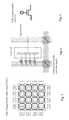
- FIG. 1shows a simplified block diagram of an FPGA.
- FIG. 2shows a larger view of an exemplary portion of the simplified block diagram of an FPGA of FIG. 1 , showing a logic block/cell, interconnects of the logic block/cell connecting to the logic block/cell and leading around the logic block/cell, and a matrix of configurable interconnections coupling these interconnects.
- FIG. 3shows a larger view of an exemplary portion of the matrix of configurable interconnections of FIG. 1 , showing one configurable interconnection of the matrix.
- FIG. 4shows the configurable interconnection of FIG. 3 , which is configurable to electrically couple or decouple interconnects 1 and 2 of the logic blocks of an FPGA.
- FIG. 5shows an example SRAM which stores the configuration information that is used to configure the configurable interconnection of FIG. 4 .
- FIG. 6shows an example circuit of a resistive memory element as the configurable interconnection coupling interconnects 1 and 2 of the logic blocks, where the resistive memory element is programmed through a field effect transistor connected to a program word line and a program bit line.
- FIG. 7shows an example circuit of a resistive memory element as the configurable interconnection coupling interconnects 1 and 2 of the logic blocks, where the resistive memory element is programmed through a bipolar junction transistor connected to a program word line and a program bit line.
- FIG. 8shows an example circuit of a resistive memory element as the configurable interconnection coupling interconnects 1 and 2 of the logic blocks, where the resistive memory element is programmed through a diode connected to a program bit line.
- FIG. 9shows an example circuit of a resistive memory element and field effect transistors as the configurable interconnection selectively coupling interconnects 1 and 2 of the logic blocks, and selectively coupling a program bit line with interconnect 1 of the logic blocks.
- FIG. 10shows an example arrangement of a phase change element as the configurable interconnection coupling interconnects 1 and 2 of the logic blocks, where the phase change element has an amorphous region through which the phase change element receives pulses from a programming circuit, and the configurable interconnection is in a shorted state, or state of low resistance, due to the small size of the amorphous region.
- FIG. 11shows an example arrangement of a phase change element as the configurable interconnection coupling interconnects 1 and 2 of the logic blocks, where the phase change element has an amorphous region through which the phase change element receives pulses from a programming circuit, and the configurable interconnection is in an open state, or state of high resistance, due to the large size of the amorphous region.
- FIG. 12shows an example arrangement of a phase change element as the configurable interconnection coupling interconnects 1 and 2 of the logic blocks, where the phase change element has an amorphous region through which the phase change element receives pulses from a programming circuit, and the phase change element is programmed through a field effect transistor connected to a program word line and a program bit line.
- FIG. 13shows an example arrangement of a phase change element as the configurable interconnection coupling interconnects 1 and 2 of the logic blocks, where the phase change element has an amorphous region through which the phase change element receives pulses from a programming circuit, the phase change element is programmed through a field effect transistor connected to a program word line and a program bit line, and interconnect 2 of the logic blocks is grounded through a field effect transistor connected to a program bit line.
- FIG. 14is a top view of an example arrangement of a phase change element as the configurable interconnection coupling interconnects 1 and 2 of the logic blocks, where the phase change element has an amorphous region through which the phase change element receives pulses from a programming circuit.
- FIG. 15is a top view of an example arrangement of a phase change element as the configurable interconnection coupling interconnects 1 and 2 of the logic blocks, where the phase change element has an amorphous region through which the phase change element receives pulses from a programming circuit, and the heater connected to the amorphous region surrounds interconnect 2 of the logic blocks.
- FIG. 16is a side view of an example arrangement of a phase change element as the configurable interconnection coupling interconnects 1 and 2 of the logic blocks, where the phase change element has an amorphous region through which the phase change element receives pulses from a programming circuit, and the heater connected to the amorphous region surrounds interconnect 2 of the logic blocks.
- FIGS. 17-23show side views of a process flow to make a phase change element as the configurable interconnection coupling interconnects 1 and 2 of the logic blocks, where the phase change element has an amorphous region through which the phase change element receives pulses from a programming circuit.
- FIGS. 24-28show top views of a process flow to make a phase change element as the configurable interconnection coupling interconnects 1 and 2 of the logic blocks, where the phase change element has an amorphous region through which the phase change element receives pulses from a programming circuit.
- FIG. 29is a functional block diagram of an example integrated circuit with the logic blocks, configurable interconnections coupling interconnects of the logic blocks, and programming circuitry of the configurable interconnections.
- PLDsProgrammable logic devices
- PLAprogrammable logic array
- PALprogrammable array logic
- EPLDerasable programmable logic devices
- PGAprogrammable gate arrays
- the field programmable gate arraytypically includes programmable logic blocks, configurable interconnections, and input/output blocks.
- the input/output blocksare fabricated on the perimeter of the die surrounding the logic blocks.
- the logic blocksperform logic functions of various complexity. Examples of the logic blocks are random access memory blocks, multipliers, digital signal processing blocks, processors, clock managers, delay lock loops, blocks of Boolean logic and/or state machine logic of various complexity, and the like.
- FIG. 1shows a simplified block diagram of an FPGA.
- FIG. 2shows a larger view of an exemplary portion of the simplified block diagram of an FPGA of FIG. 1 , showing a logic block/cell, interconnects of the logic block/cell connecting to the logic block/cell and leading around the logic block/cell, and a matrix of configurable interconnections coupling these interconnects.
- FIG. 3shows a larger view of an exemplary portion of the matrix of configurable interconnections of FIG. 1 , showing one configurable interconnection of the matrix.
- FIG. 4shows the configurable interconnection of FIG. 3 , which is configurable to electrically couple or decouple interconnects 1 and 2 of the logic blocks of an FPGA.
- FIG. 5shows an example SRAM which stores the configuration information that is used to configure the configurable interconnection of FIG. 4 .
- FIG. 6shows an example circuit of a resistive memory element as the configurable interconnection coupling interconnects 1 and 2 of the logic blocks, where the resistive memory element is programmed through a field effect transistor connected to a program word line and a program bit line.
- both the programming word line and the programming bit linehave Vcc, and both the interconnects 1 and 2 are grounded.
- the programming word lineis grounded.
- FIG. 7shows an example circuit of a resistive memory element as the configurable interconnection coupling interconnects 1 and 2 of the logic blocks, where the resistive memory element is programmed through a bipolar junction transistor connected to a program word line and a program bit line.
- the programming word linehas one half Vcc, the programming bit line has Vcc, and both the interconnects 1 and 2 are grounded.
- the programming word lineis grounded.
- FIG. 8shows an example circuit of a resistive memory element as the configurable interconnection coupling interconnects 1 and 2 of the logic blocks, where the resistive memory element is programmed through a diode connected to a program bit line.
- the programming word linehas one half Vcc, the programming bit line has Vcc, and both the interconnects 1 and 2 are grounded.
- the programming word lineis grounded.
- FIG. 9shows an example circuit of a resistive memory element and field effect transistors as the configurable interconnection selectively coupling interconnects 1 and 2 of the logic blocks, and selectively coupling a program bit line with interconnect 1 of the logic blocks.
- interconnect line 2 and a programming bit lineBetween interconnect line 2 and a programming bit line, a p-type FET and an n-type FET are connected in series.
- the interconnect line 2is on the p-type FET side and the programming bit line is on the n-type FET side.
- the gates of both the p-type FET and the n-type FETare connected to a programming word line.
- a programmable resistive memory elementhas one end connected between the p-type FET and the n-type FET, and the other end connected to interconnect line 1 .
- Examples of the n-type FET and p-type FETare NMOS and PMOS transistors.
- the positions of the n-type and p-type FETsare exchanged, and the logic of the programming word line is altered to exchange logically high and logically low values.
- Interconnect 1is grounded. The result is that the NMOS turns on, and the PMOS turns off. Interconnect 2 is isolated from the programming circuitry path and interconnect 1 .
- the programming word line, and the programming bit lineare grounded. The result is that the NMOS turns off, and the PMOS turns on. The logic path of the interconnects is isolated from the programming circuitry by the NMOS.
- Reading or writing to a phase change memory cell embodiment of a resistive memory elementcan be achieved by applying an appropriate voltage to the corresponding word line and an appropriate voltage or current to the corresponding bit line to induce a current through the memory element.
- the level and duration of the voltages/currents appliedis dependent upon the operation performed, e.g. a reading operation or a writing operation.
- a reset pulse applied to the word line and the bit lineinduces a current through the memory element to cause a transition of an active region of the memory element into an amorphous phase, thereby setting the phase change material to a resistance within a resistance value range associated with the reset state.
- the reset pulseis a relatively high energy pulse, sufficient to raise the temperature of at least the active region of the memory element above the transition (crystallization) temperature of the phase change material and also above the melting temperature to place at least the active region in a liquid state.
- the reset pulseis then quickly terminated, resulting in a relatively quick quenching time as the active region quickly cools to below the transition temperature so that the active region stabilizes to a generally amorphous phase.
- a program pulseis applied to the word line and the bit line of suitable amplitude and duration to induce a current through the memory element sufficient to raise the temperature of at least a portion of the active region of the memory element above the transition temperature and cause a transition of at least a portion of the active region from the amorphous phase into a crystalline phase, this transition lowering the resistance of the memory element and setting the memory cell to the desired state.
- a read pulseapplied to the corresponding word line and the corresponding bit line of suitable amplitude and duration to induce current to flow through the memory element that does not result in the memory element undergoing a change in resistive state.
- the current through the memory cellis dependent upon the resistance of the memory element and thus the data value stored in the memory cell.
- the data valued stored in the memory cellmay be determined, for example, by comparison of the current on bit line with a suitable reference current by sense amplifiers.
- the data value stored in the memory cellmay be determined, for example, using source side sensing by comparison of the current on the conductive material of the memory plane with a suitable reference current.
- a configurable interconnectionincludes a resistive memory element.
- Programmable resistance memory materialsinclude materials that use different crystal phase changes to determine resistance, or memory materials that use an electrical pulse to change the resistance state. Examples include materials for use in resistance random access memory (RRAM) such as metal-oxides including tungsten-oxide (WO x ), NiO, Nb 2 O 5 , CuO 2 , Ta 2 O 5 , Al 2 O 3 , CoO, Fe 2 O 3 , HfO 2 , TiO 2 , SrTiO 3 , SrZrO 3 , (BaSr)TiO 3 .
- RRAMresistance random access memory
- MRAMmagnetoresistance random access memory
- STTspin-torque-transfer
- Additional examplesinclude solid electrolyte materials used for programmable-metallization-cell (PMC) memory, or nano-ionic memory, such as silver-doped germanium sulfide electrolytes and copper-doped germanium sulfide electrolytes.
- PMCprogrammable-metallization-cell
- nano-ionic memorysuch as silver-doped germanium sulfide electrolytes and copper-doped germanium sulfide electrolytes.
- Embodiments of the programmable resistance material of the memory elementsinclude phase-change-based memory materials, including chalcogenide based materials and other materials.
- Chalcogensinclude any of the four elements oxygen (O), sulfur (S), selenium (Se), and tellurium (Te), forming part of group VIA of the periodic table.
- Chalcogenidescomprise compounds of a chalcogen with a more electropositive element or radical.
- Chalcogenide alloyscomprise combinations of chalcogenides with other materials such as transition metals.
- a chalcogenide alloyusually contains one or more elements from group IVA of the periodic table of elements, such as germanium (Ge) and tin (Sn).
- chalcogenide alloysinclude combinations including one or more of antimony (Sb), gallium (Ga), indium (In), and silver (Ag).
- Sbantimony
- Gagallium
- Inindium
- silverAg.
- phase-change-based memory materialshave been described in technical literature, including alloys of: Ga/Sb, In/Sb, In/Se, Sb/Te, Ge/Te, Ge/Sb/Te, In/Sb/Te, Ga/Se/Te, Sn/Sb/Te, In/Sb/Ge, Ag/In/Sb/Te, Ge/Sn/Sb/Te, Ge/Sb/Se/Te and Te/Ge/Sb/S.
- compositionscan be workable.
- the compositionscan be characterized as Te a Ge b Sb 100-(a+b) .
- One researcherhas described the most useful alloys as having an average concentration of Te in the deposited materials well below 70%, typically below about 60% and ranged in general from as low as about 23% up to about 58% Te and most preferably about 48% to 58% Te.
- Concentrations of Gewere above about 5% and ranged from a low of about 8% to about 30% average in the material, remaining generally below 50%. Most preferably, concentrations of Ge ranged from about 8% to about 40%. The remainder of the principal constituent elements in this composition was Sb.
- a transition metalsuch as chromium (Cr), iron (Fe), nickel (Ni), niobium (Nb), palladium (Pd), platinum (Pt) and mixtures or alloys thereof may be combined with Ge/Sb/Te to form a phase change alloy that has programmable resistance properties.
- chromium (Cr)iron (Fe), nickel (Ni), niobium (Nb), palladium (Pd), platinum (Pt) and mixtures or alloys thereof
- Ge/Sb/TeGe/Sb/Te
- Specific examples of memory materials that may be usefulare given in Ovshinsky '112 at columns 11-13, which examples are hereby incorporated by reference.
- Chalcogenides and other phase change materialsare doped with impurities in some embodiments to modify conductivity, transition temperature, melting temperature, and other properties of memory elements using the doped chalcogenides.
- Representative impurities used for doping chalcogenidesinclude nitrogen, silicon, oxygen, silicon dioxide, silicon nitride, copper, silver, gold, aluminum, aluminum oxide, tantalum, tantalum oxide, tantalum nitride, titanium and titanium oxide. See, e.g., U.S. Pat. No. 6,800,504, and U.S. Patent Application Publication No. U.S. 2005/0029502.
- Phase change alloyscan be changed from one phase state to another by application of electrical pulses. It has been observed that a shorter, higher amplitude pulse tends to change the phase change material to a generally amorphous state. A longer, lower amplitude pulse tends to change the phase change material to a generally crystalline state. The energy in a shorter, higher amplitude pulse is high enough to allow for bonds of the crystalline structure to be broken and short enough to prevent the atoms from realigning into a crystalline state. Appropriate profiles for pulses can be determined, without undue experimentation, specifically adapted to a particular phase change alloy. In following sections of the disclosure, the phase change material is referred to as GST, and it will be understood that other types of phase change materials can be used. A material useful for implementation of a PCRAM described herein is Ge 2 Sb 2 Te 5 .
- An exemplary method for forming chalcogenide materialuses PVD-sputtering or magnetron-sputtering method with source gas(es) of Ar, N 2 , and/or He, etc. at the pressure of 1 mTorr ⁇ 100 mTorr.
- the depositionis usually done at room temperature.
- a collimator with an aspect ratio of 1 ⁇ 5can be used to improve the fill-in performance.
- a DC bias of several tens of volts to several hundreds of voltsis also used.
- a combination of DC bias and a collimatorcan be used.
- An exemplary method for forming chalcogenide materialuses chemical vapor deposition CVD such as that disclosed in US Publication No 2006/0172067 entitled “Chemical Vapor Deposition of Chalcogenide Materials,” which is incorporated by reference herein.
- a post-deposition annealing treatment in a vacuum or in an N 2 ambientis optionally performed to improve the crystallize state of chalcogenide material.
- the annealing temperaturetypically ranges from 100° C. to 400° C. with an anneal time of less than 30 minutes.
- FIGS. 10-16feature multiple similar reset pulses of a relatively high energy and short duration to result in different states of (i) shorted state or state of low resistance and (ii) open state or state of high resistance.
- the pulseshave a magnitude ranging from 1V-5V in magnitude and 1 ns to 100 ns in duration. Regardless of the particular state following a particular reset pulse, applying a set pulse readies resistive memory element for a subsequent application of one of the multiple similar reset pulses.
- FIG. 10shows an example arrangement of a phase change element as the configurable interconnection coupling interconnects 1 and 2 of the logic blocks, where the phase change element has an amorphous region through which the phase change element receives pulses from a programming circuit, and the configurable interconnection is in a shorted state, or state of low resistance, due to the small size of the amorphous region.
- FIG. 11shows an example arrangement of a phase change element as the configurable interconnection coupling interconnects 1 and 2 of the logic blocks, where the phase change element has an amorphous region through which the phase change element receives pulses from a programming circuit, and the configurable interconnection is in an open state, or state of high resistance, due to the large size of the amorphous region.
- FIG. 12shows an example arrangement of a phase change element as the configurable interconnection coupling interconnects 1 and 2 of the logic blocks, where the phase change element has an amorphous region through which the phase change element receives pulses from a programming circuit, and the phase change element is programmed through a field effect transistor connected to a program word line and a program bit line.
- FIG. 13shows an example arrangement of a phase change element as the configurable interconnection coupling interconnects 1 and 2 of the logic blocks, where the phase change element has an amorphous region through which the phase change element receives pulses from a programming circuit, the phase change element is programmed through a field effect transistor connected to a program word line and a program bit line, and interconnect 2 of the logic blocks is grounded through a field effect transistor connected to a program bit line.
- FIG. 14is a top view of an example arrangement of a phase change element as the configurable interconnection coupling interconnects 1 and 2 of the logic blocks, where the phase change element has an amorphous region through which the phase change element receives pulses from a programming circuit.
- FIG. 15is a top view of an example arrangement of a phase change element as the configurable interconnection coupling interconnects 1 and 2 of the logic blocks, where the phase change element has an amorphous region through which the phase change element receives pulses from a programming circuit, and the heater connected to the amorphous region surrounds interconnect 2 of the logic blocks. This embodiment saves one mask step.
- FIG. 16is a side view of an example arrangement of a phase change element as the configurable interconnection coupling interconnects 1 and 2 of the logic blocks, where the phase change element has an amorphous region through which the phase change element receives pulses from a programming circuit, and the heater connected to the amorphous region surrounds interconnect 2 of the logic blocks.
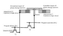
- a programming pathincludes the programming bit line BL which connects, through a via, to the transistor source/drain S/D.
- the other transistor source/drain S/Dconnects, through another via, to a heater.
- the heatersurrounds interconnect 2 and connects to the amorphous region of a phase change element.
- the phase change elementphysically connects interconnect 1 and interconnect 2 .
- Interconnect 2is on multiple levels, connected by a via.
- FIGS. 17-23show side views of a process flow to make a phase change element as the configurable interconnection coupling interconnects 1 and 2 of the logic blocks, where the phase change element has an amorphous region through which the phase change element receives pulses from a programming circuit.
- shallow trench isolation (STI) structures 14 and 15electrically isolate the field effect transistor in between, from neighboring electrical devices.
- Substrate material(alternatively a doped n-well or p-well) 12 is positioned between the STI structures 14 and 15 .
- the field effect transistorincludes a portion of the material 12 as the body, source and drain regions 16 and 17 , and a programming word line 18 as the gate.
- the word line materialcan be a doped polysilicon, or other conductive material such as titanium nitride or other conductive nitride, tungsten, or other metal. Also, combinations of such materials can be used.
- Conductive via 20 and bit line 21electrically connect to the source and drain regions 16 and 17 .
- Dielectric fill material 22 , 23 , and 24surround the conductive vias 20 and 21 .
- Heater and interconnect material layer 26is formed to cover the structure.
- photolithographically patterned layer 28is formed on the heater and interconnect material layer 26 .
- the photolithographically patterned mask layer 28allows selective etching of the heater and interconnect material layer 26 areas unprotected by the photolithographically patterned layer 28 .
- the remainder after etchingis the heater 33 and interconnects 32 and 34 .
- the heater 33has an electrical resistivity greater than that of the material of the via 20 .
- the material of the heater 33may also, for example, comprise a material having a resistivity greater than that of the highest resistance state of the material of the memory element to be formed.
- the heater 33comprises doped semiconductor material.
- Interconnects 32 and 34are the different interconnects leading to the logic blocks of a programmable logic device.
- interconnects 32 and 34are the same material as heater 33 for efficient manufacture, alternatively the interconnects 32 and 34 are different material as heater 33 , at the cost of additional steps. In such an embodiment with different materials, interconnects 32 and 34 are any suitable conductive material.
- dielectric fill material 36is deposited to surround the heater 33 and interconnects 32 and 34 , with excess dielectric fill material removed by a planarization process such as Chemical Mechanical Polishing (CMP).
- CMPChemical Mechanical Polishing
- phase change element 38is formed on top of the structure, to connect with the heater 33 and interconnects 32 and 34 .
- Forming a bridge phase change element 38is discussed in U.S. Pat. No. 7,459,717 by Hsian-Lan Lung, incorporated herein by reference.
- vias 40 and 41are formed that connect with interconnects 32 and 34 .
- Dielectric fill material 42 and 43is deposited around the vias 40 and 41 , with excess dielectric fill material removed by a planarization process such as Chemical Mechanical Polishing (CMP).
- CMPChemical Mechanical Polishing
- via 50 connecting to via 40and interconnect 51 connecting to via 41 are formed.
- Dielectric fill material 52is deposited between via 50 and interconnect 51 , and the excess removed.
- Interconnect 60is formed to connect to via 50 .
- Dielectric fill material 62is deposited next to via 50 , and the excess removed.
- Interconnects 51 and 60connect to the logic blocks of the programmable logic device
- Dielectric fill material 42 and 43is deposited to surround the vias 40 and 41 , with excess dielectric fill material removed by a planarization process such as Chemical Mechanical Polishing (CMP).
- CMPChemical Mechanical Polishing
- FIGS. 24-28show top views of a process flow to make a phase change element as the configurable interconnection coupling interconnects 1 and 2 of the logic blocks, where the phase change element has an amorphous region through which the phase change element receives pulses from a programming circuit.
- word line 18is formed on an active region, separating source and drain regions 16 and 17 .
- the word line 18is part of the programming circuitry for the configurable interconnect.
- Source and drain regions 16 and 17are in a substrate 12 .
- bit line 21is part of the programming circuitry for the configurable interconnect.
- interconnects 32 and 34are formed in FIG. 26 .
- Heater 33connects with the via 20 .
- interconnect 32appears over word line 18 , interconnect 32 and word line 18 are separated by intervening fill dielectric.
- phase change element 38is formed on interconnects 32 and 34 , and heater 33 .
- vias 40 and 41are formed to connect to interconnects 32 and 34 . Subsequently, interconnects to the logic blocks are formed, that lead to the logic blocks of the programmable logic device.
- FIG. 29is a functional block diagram of an example programmable logic device integrated circuit with the logic blocks, configurable interconnections coupling interconnects of the logic blocks, and programming circuitry of the configurable interconnections.
- the programmable logic device integrated circuit 2950has several functional blocks (shown separately for convenience, although each functional block is physically spread out around the integrated circuit and interconnected numerous times with the other functional blocks).
- Logic blocks 2900are connected by the configurable interconnections 2908 .
- the configurable interconnections 2908are programmed by the programming circuitry 2910 .
- the programming circuitry 2910includes, in addition to programming bit lines and programming word lines, control circuitry that implements the change of state of the configurable interconnections 2908 , by sending the various pulses through the programming bit line and the control signals through the programming word lines.
Landscapes
- Chemical & Material Sciences (AREA)
- Crystallography & Structural Chemistry (AREA)
- Semiconductor Memories (AREA)
Abstract
Description
1. Field of the Invention
This technology relates to a configurable interconnection coupling interconnects, and a programmable logic device with such configurable interconnections.
2. Description of Related Art
In the field programmable gate array (FPGA) device described by U.S. Pat. Nos. 7,307,451 and 7,511,523; and U.S. Patent Application Publication No. 2007/0146012, a phase change material storage element is part of a control unit that stores settings of the configurable interconnections of the FPGA. The control unit is distinct from the actual configurable interconnections of the FPGA. Every time the FPGA is turned on, the contents of the control unit are read, and used to determine the settings of the configurable interconnections of the FPGA.
In the programmable matrix of an FPGA device described by U.S. Pat. No. 7,499,315 and U.S. Patent Application Publication No. 2006/0171194, a phase change material storage element is again part of a control cell, distinct from the actual configurable interconnections of the FPGA. Also discussed is the use of anti-fuse devices that directly connect a vertical interconnect and a horizontal interconnect. Such anti-fuse devices are programmed via signals through the very same vertical interconnect and horizontal interconnect that are coupled by the anti-fuse device. Because programming circuitry for the anti-fuse devices is connected to the same interconnects for logical operations, the interconnects have an additional RC delay associated with the programming circuitry load.
One aspect of the technology is an apparatus includes a programmable logic device having logic blocks, configurable interconnections coupling interconnects of the logic blocks, and programming circuitry of the configurable interconnections. The configurable interconnections include phase change elements. Each phase change element is coupling a first interconnect and a second interconnect of the logic blocks. Each phase change element includes an amorphous region. The amorphous region is connected to a heater to receive pulses from the programming circuitry. The amorphous region electrically isolates the heater from the first interconnect and the second interconnect. The pulses are received from the programming circuitry via a path distinct from the first interconnect and the second interconnect of the logic blocks.
In some embodiments, the amorphous region electrically isolates the first interconnect and the second interconnect of the logic blocks from the programming circuitry. When the phase change element receives pulses from the programming circuitry via the amorphous region, because the amorphous region is a high resistance region, the remaining non-amorphous region (e.g., crystalline region) of the phase change element is electrically isolated from the programming circuitry. Similarly, the interconnects of the logic blocks that are electrically connected to the non-amorphous region (e.g., crystalline region) of the phase change element are electrically isolated from the programming circuitry. Because of the electrical isolation of the interconnects of the logic blocks from the programming circuitry, the interconnects of the logic blocks are free of the RC delay which would otherwise result from the programming circuitry load.
In some embodiments, each phase change element has multiple electrical resistance states. A first state has low electrical resistance between the first interconnect and the second interconnect, responsive to the amorphous region having a first size. A second state has a second electrical resistance between the first interconnect and the second interconnect. Responsive to the amorphous region having a second size larger than the first size, the second electrical resistance is higher than the first electrical resistance.
In some embodiments, the programming circuitry is configured to apply the pulses, including pulses of different electrical characteristics. For example, a first reset pulse and a second reset pulse of different electrical characteristics result in a variable size of the amorphous region. In one embodiment, the first reset pulse and the second reset pulse have a same duration. An example of the same duration for the first reset pulse and the second reset pulse is a value in the range between 1-50 nanoseconds. In another embodiment, the first reset pulse and the second reset pulse have different voltages. In yet another embodiment, the first reset pulse and the second reset pulse have a same duration but different voltages.
Some embodiments include grounding transistors electrically coupled to the interconnects of the logic blocks. The grounding transistors electrically isolate the interconnects from the programming circuitry. For example, a programming bit line turns on the grounding transistor to electrically ground the interconnects during programming of the configurable interconnections.
Some embodiments include the heater connected to the amorphous region and in the path receiving pulses from the programming circuitry.
Another aspect of the technology is an apparatus including a switch coupling a first node and a second node, as described herein.
One aspect of the technology is an apparatus including a programmable logic device having logic blocks, configurable interconnections coupling interconnects of the logic blocks, and programming circuitry of the configurable interconnections. The programming circuitry has program word lines and program bit lines. The configurable interconnections each include a resistive memory element, and a first transistor and a second transistor of opposite conductivity types, such as a p-type field effect transistor and an n-type field effect transistor.
The resistive memory element has different states to selectably electrically couple a first interconnect and a second interconnect of the logic blocks, such that depending on the state of the resistive memory element, the first interconnect and a second interconnect of the logic blocks are electrically coupled or decoupled. The resistive memory element includes a first end electrically coupled to the first interconnect of the logic blocks, and a second end electrically coupled to a first current carrying terminal of both the first transistor and the second transistor. For example, the second end of the resistive memory element is electrically coupled to a source/drain terminal of a p-type field effect transistor and a source/drain terminal of an n-type field effect transistor.
The first transistor has a control terminal, the first current carrying terminal, and a second current carrying terminal electrically coupled to the second interconnect of the logic blocks. As previously stated, the first current carrying terminal is electrically coupled to the second end of the resistive memory element. For example, the first transistor is a p-type field effect transistor with a gate terminal, the source/drain terminal electrically coupled to the second end of the resistive memory element, and a drain/source terminal electrically coupled to the second interconnect of the logic blocks.
The second transistor having a control terminal, the first current carrying terminal, and a second current carrying terminal electrically coupled to a program bit line of the programming circuitry. As previously stated, the first current carrying terminal is electrically coupled to the second end of the resistive memory element. For example, the second transistor is an n-type field effect transistor with a gate terminal, the source/drain terminal electrically coupled to the second end of the resistive memory element, and a drain/source terminal electrically coupled to a program bit line of the programming circuitry.
The control terminals of both the first transistor and the second transistor are electrically coupled to a same program word line of the programming circuitry. For example, the gates of both the p-type field effect transistor and the n-type field effect transistor are electrically coupled to a same program word line of the programming circuitry.
In some embodiments, during operation of the logic blocks, the programmable logic device includes control circuitry that applies a voltage to the same program word line to turn on the first transistor and turn off the second transistor. For example, a low or ground voltage applied to the same program word line turns on the p-type transistor and turns off the n-type transistor. During operation of the logic blocks, the second transistor (e.g., the n-type transistor), in its off state, isolates the program bit line (on one side of the second transistor) from the resistive memory element, the first interconnect, and the second interconnect (on the other side of the second transistor).
In some embodiments, during programming of the resistive memory element, the programmable logic device includes control circuitry that applies a voltage to the same program word line to turn off the first transistor and turn on the second transistor. For example, a high voltage applied to the same program word line turns off the p-type transistor and turns on the n-type transistor. During programming of the resistive memory element, the first transistor (e.g., the p-type transistor) isolates the second interconnect (on one side of the first transistor) from the resistive memory element and the program bit line (on the other side of the first transistor).
Accordingly, in many embodiments, during normal operation of the configurable interconnections including programming of the resistive memory element and operation of the logic blocks, either only the first transistor is on, or only the second transistor is on.
Another aspect of the technology is an apparatus including a configurable interconnection including a resistive memory element, and a first transistor and a second transistor of opposite conductivity types, as described herein.
Programmable logic devices (PLDs) are a type of integrated circuit that can be programmed to perform specified logic functions. PLDs include programmable logic array (PLA) devices, programmable array logic (PAL) devices, erasable programmable logic devices (EPLD), and programmable gate arrays (PGA).
One type of PLD, the field programmable gate array (FPGA), typically includes programmable logic blocks, configurable interconnections, and input/output blocks. In one implementation on an integrated circuit, the input/output blocks are fabricated on the perimeter of the die surrounding the logic blocks. The logic blocks perform logic functions of various complexity. Examples of the logic blocks are random access memory blocks, multipliers, digital signal processing blocks, processors, clock managers, delay lock loops, blocks of Boolean logic and/or state machine logic of various complexity, and the like. By programming the configurable interconnections coupling the logic blocks, the programmed logic functions of individual configurable logic blocks can be coupled together to implement more complex and customized logic functions.
Different bias conditions are shown. To program the resistive memory element, both the programming word line and the programming bit line have Vcc, and both theinterconnects
Different bias conditions are shown. To program the resistive memory element, the programming word line has one half Vcc, the programming bit line has Vcc, and both theinterconnects
Different bias conditions are shown. To program the resistive memory element, the programming word line has one half Vcc, the programming bit line has Vcc, and both theinterconnects
Betweeninterconnect line 2 and a programming bit line, a p-type FET and an n-type FET are connected in series. Theinterconnect line 2 is on the p-type FET side and the programming bit line is on the n-type FET side. The gates of both the p-type FET and the n-type FET are connected to a programming word line. A programmable resistive memory element has one end connected between the p-type FET and the n-type FET, and the other end connected to interconnectline 1. Examples of the n-type FET and p-type FET are NMOS and PMOS transistors. In another embodiment, the positions of the n-type and p-type FETs are exchanged, and the logic of the programming word line is altered to exchange logically high and logically low values.
During programming, the programming word line, and programming bit line have Vdd.Interconnect 1 is grounded. The result is that the NMOS turns on, and the PMOS turns off.Interconnect 2 is isolated from the programming circuitry path andinterconnect 1.
During logic operations, the programming word line, and the programming bit line are grounded. The result is that the NMOS turns off, and the PMOS turns on. The logic path of the interconnects is isolated from the programming circuitry by the NMOS.
The following discusses memory operations of a phase change memory cell generally. Reading or writing to a phase change memory cell embodiment of a resistive memory element can be achieved by applying an appropriate voltage to the corresponding word line and an appropriate voltage or current to the corresponding bit line to induce a current through the memory element. The level and duration of the voltages/currents applied is dependent upon the operation performed, e.g. a reading operation or a writing operation.
In a reset (erase) operation of the phase change memory cell, a reset pulse applied to the word line and the bit line induces a current through the memory element to cause a transition of an active region of the memory element into an amorphous phase, thereby setting the phase change material to a resistance within a resistance value range associated with the reset state. The reset pulse is a relatively high energy pulse, sufficient to raise the temperature of at least the active region of the memory element above the transition (crystallization) temperature of the phase change material and also above the melting temperature to place at least the active region in a liquid state. The reset pulse is then quickly terminated, resulting in a relatively quick quenching time as the active region quickly cools to below the transition temperature so that the active region stabilizes to a generally amorphous phase.
In a set (or program) operation of phase change memory cell, a program pulse is applied to the word line and the bit line of suitable amplitude and duration to induce a current through the memory element sufficient to raise the temperature of at least a portion of the active region of the memory element above the transition temperature and cause a transition of at least a portion of the active region from the amorphous phase into a crystalline phase, this transition lowering the resistance of the memory element and setting the memory cell to the desired state.
In a read (or sense) operation of the data value stored in the memory cell, a read pulse applied to the corresponding word line and the corresponding bit line of suitable amplitude and duration to induce current to flow through the memory element that does not result in the memory element undergoing a change in resistive state. The current through the memory cell is dependent upon the resistance of the memory element and thus the data value stored in the memory cell. The data valued stored in the memory cell may be determined, for example, by comparison of the current on bit line with a suitable reference current by sense amplifiers. Alternatively, the data value stored in the memory cell may be determined, for example, using source side sensing by comparison of the current on the conductive material of the memory plane with a suitable reference current.
In various embodiments, a configurable interconnection includes a resistive memory element. Programmable resistance memory materials include materials that use different crystal phase changes to determine resistance, or memory materials that use an electrical pulse to change the resistance state. Examples include materials for use in resistance random access memory (RRAM) such as metal-oxides including tungsten-oxide (WOx), NiO, Nb2O5, CuO2, Ta2O5, Al2O3, CoO, Fe2O3, HfO2, TiO2, SrTiO3, SrZrO3, (BaSr)TiO3. Additional examples include materials for use in magnetoresistance random access memory (MRAM) such as spin-torque-transfer (STT) MRAM, for example at least one of CoFeB, Fe, Co, Ni, Gd, Dy, CoFe, NiFe, MnAs, MnBi, MnSb, CrO2, MnOFe2O3, FeOFe2O5, NiOFe2O3, MgOFe2, EuO, and Y3Fe5O12. See, for example, US Publication No 2007/0176251 entitled “Magnetic Memory Device and Method of Fabricating the Same,” which is incorporated by reference herein. Additional examples include solid electrolyte materials used for programmable-metallization-cell (PMC) memory, or nano-ionic memory, such as silver-doped germanium sulfide electrolytes and copper-doped germanium sulfide electrolytes. See, for example, N. E. Gilbert et al., “A macro model of programmable metallization cell devices,” Solid-State Electronics 49 (2005) 1813-1819, which is incorporated by reference herein.
Embodiments of the programmable resistance material of the memory elements include phase-change-based memory materials, including chalcogenide based materials and other materials. Chalcogens include any of the four elements oxygen (O), sulfur (S), selenium (Se), and tellurium (Te), forming part of group VIA of the periodic table. Chalcogenides comprise compounds of a chalcogen with a more electropositive element or radical. Chalcogenide alloys comprise combinations of chalcogenides with other materials such as transition metals. A chalcogenide alloy usually contains one or more elements from group IVA of the periodic table of elements, such as germanium (Ge) and tin (Sn). Often, chalcogenide alloys include combinations including one or more of antimony (Sb), gallium (Ga), indium (In), and silver (Ag). Many phase-change-based memory materials have been described in technical literature, including alloys of: Ga/Sb, In/Sb, In/Se, Sb/Te, Ge/Te, Ge/Sb/Te, In/Sb/Te, Ga/Se/Te, Sn/Sb/Te, In/Sb/Ge, Ag/In/Sb/Te, Ge/Sn/Sb/Te, Ge/Sb/Se/Te and Te/Ge/Sb/S. In the family of Ge/Sb/Te alloys, a wide range of alloy compositions may be workable. The compositions can be characterized as TeaGebSb100-(a+b). One researcher has described the most useful alloys as having an average concentration of Te in the deposited materials well below 70%, typically below about 60% and ranged in general from as low as about 23% up to about 58% Te and most preferably about 48% to 58% Te. Concentrations of Ge were above about 5% and ranged from a low of about 8% to about 30% average in the material, remaining generally below 50%. Most preferably, concentrations of Ge ranged from about 8% to about 40%. The remainder of the principal constituent elements in this composition was Sb. These percentages are atomic percentages that total 100% of the atoms of the constituent elements. (Ovshinsky U.S. Pat. No. 5,687,112, cols. 10-11.) Particular alloys evaluated by another researcher include Ge2Sb2Te5, GeSb2Te4and GeSb4Te7(Noboru Yamada, “Potential of Ge—Sb—Te Phase-Change Optical Disks for High-Data-Rate Recording”, SPIE v.3109, pp. 28-37 (1997).) More generally, a transition metal such as chromium (Cr), iron (Fe), nickel (Ni), niobium (Nb), palladium (Pd), platinum (Pt) and mixtures or alloys thereof may be combined with Ge/Sb/Te to form a phase change alloy that has programmable resistance properties. Specific examples of memory materials that may be useful are given in Ovshinsky '112 at columns 11-13, which examples are hereby incorporated by reference.
Chalcogenides and other phase change materials are doped with impurities in some embodiments to modify conductivity, transition temperature, melting temperature, and other properties of memory elements using the doped chalcogenides. Representative impurities used for doping chalcogenides include nitrogen, silicon, oxygen, silicon dioxide, silicon nitride, copper, silver, gold, aluminum, aluminum oxide, tantalum, tantalum oxide, tantalum nitride, titanium and titanium oxide. See, e.g., U.S. Pat. No. 6,800,504, and U.S. Patent Application Publication No. U.S. 2005/0029502.
Phase change alloys can be changed from one phase state to another by application of electrical pulses. It has been observed that a shorter, higher amplitude pulse tends to change the phase change material to a generally amorphous state. A longer, lower amplitude pulse tends to change the phase change material to a generally crystalline state. The energy in a shorter, higher amplitude pulse is high enough to allow for bonds of the crystalline structure to be broken and short enough to prevent the atoms from realigning into a crystalline state. Appropriate profiles for pulses can be determined, without undue experimentation, specifically adapted to a particular phase change alloy. In following sections of the disclosure, the phase change material is referred to as GST, and it will be understood that other types of phase change materials can be used. A material useful for implementation of a PCRAM described herein is Ge2Sb2Te5.
An exemplary method for forming chalcogenide material uses PVD-sputtering or magnetron-sputtering method with source gas(es) of Ar, N2, and/or He, etc. at the pressure of 1 mTorr˜100 mTorr. The deposition is usually done at room temperature. A collimator with an aspect ratio of 1˜5 can be used to improve the fill-in performance. To improve the fill-in performance, a DC bias of several tens of volts to several hundreds of volts is also used. Also, a combination of DC bias and a collimator can be used.
An exemplary method for forming chalcogenide material uses chemical vapor deposition CVD such as that disclosed in US Publication No 2006/0172067 entitled “Chemical Vapor Deposition of Chalcogenide Materials,” which is incorporated by reference herein.
A post-deposition annealing treatment in a vacuum or in an N2ambient is optionally performed to improve the crystallize state of chalcogenide material. The annealing temperature typically ranges from 100° C. to 400° C. with an anneal time of less than 30 minutes.
The embodiments shown inFIGS. 10-16 feature multiple similar reset pulses of a relatively high energy and short duration to result in different states of (i) shorted state or state of low resistance and (ii) open state or state of high resistance. The pulses have a magnitude ranging from 1V-5V in magnitude and 1 ns to 100 ns in duration. Regardless of the particular state following a particular reset pulse, applying a set pulse readies resistive memory element for a subsequent application of one of the multiple similar reset pulses.
This is different from many other applications, which rely on very different reset and set pulses to result in different states, in particular (i) a reset pulse of a relatively high energy and short duration to result in an open state or state of high resistance, and (ii) a set pulse of a relatively low energy and long duration to result in a shorted state or state of low resistance.
A programming path includes the programming bit line BL which connects, through a via, to the transistor source/drain S/D. The other transistor source/drain S/D connects, through another via, to a heater. The heater surroundsinterconnect 2 and connects to the amorphous region of a phase change element. The phase change element physically connectsinterconnect 1 andinterconnect 2.Interconnect 2 is on multiple levels, connected by a via.
InFIG. 17 , shallow trench isolation (STI)structures 14 and15 electrically isolate the field effect transistor in between, from neighboring electrical devices. Substrate material (alternatively a doped n-well or p-well)12 is positioned between theSTI structures 14 and15. The field effect transistor includes a portion of the material12 as the body, source and drainregions programming word line 18 as the gate. In representative embodiments, the word line material can be a doped polysilicon, or other conductive material such as titanium nitride or other conductive nitride, tungsten, or other metal. Also, combinations of such materials can be used. Conductive via20 and bitline 21 electrically connect to the source and drainregions Dielectric fill material conductive vias
InFIG. 18 , photolithographically patternedlayer 28 is formed on the heater and interconnect material layer26.
InFIG. 19 , the photolithographicallypatterned mask layer 28 allows selective etching of the heater and interconnect material layer26 areas unprotected by the photolithographicallypatterned layer 28. The remainder after etching is theheater 33 and interconnects32 and34. In some embodiments theheater 33 has an electrical resistivity greater than that of the material of the via20. The material of theheater 33 may also, for example, comprise a material having a resistivity greater than that of the highest resistance state of the material of the memory element to be formed. In certain embodiments theheater 33 comprises doped semiconductor material.Interconnects interconnects heater 33 for efficient manufacture, alternatively theinterconnects heater 33, at the cost of additional steps. In such an embodiment with different materials, interconnects32 and34 are any suitable conductive material.
InFIG. 20 ,dielectric fill material 36 is deposited to surround theheater 33 and interconnects32 and34, with excess dielectric fill material removed by a planarization process such as Chemical Mechanical Polishing (CMP).
InFIG. 21 , thephase change element 38 is formed on top of the structure, to connect with theheater 33 and interconnects32 and34. Forming a bridgephase change element 38 is discussed in U.S. Pat. No. 7,459,717 by Hsian-Lan Lung, incorporated herein by reference.
InFIG. 22 , vias40 and41 are formed that connect withinterconnects Dielectric fill material vias
InFIG. 23 , via50 connecting to via40, and interconnect51 connecting to via41 are formed.Dielectric fill material 52 is deposited between via50 and interconnect51, and the excess removed. Interconnect60 is formed to connect to via50.Dielectric fill material 62 is deposited next to via50, and the excess removed. Interconnects51 and60 connect to the logic blocks of the programmable logic device
InFIG. 24 ,word line 18 is formed on an active region, separating source and drainregions word line 18 is part of the programming circuitry for the configurable interconnect. Source anddrain regions substrate 12.
InFIG. 25 , via20 and abit line 21 are formed on source and drainregions bit line 21 is part of the programming circuitry for the configurable interconnect.
InFIG. 26 , interconnects32 and34, andheater 33 are formed.Heater 33 connects with the via20. Althoughinterconnect 32 appears overword line 18,interconnect 32 andword line 18 are separated by intervening fill dielectric.
InFIG. 27 , aphase change element 38 is formed oninterconnects heater 33.
InFIG. 28 , vias40 and41 are formed to connect tointerconnects
The programmable logic device integratedcircuit 2950 has several functional blocks (shown separately for convenience, although each functional block is physically spread out around the integrated circuit and interconnected numerous times with the other functional blocks). Logic blocks2900 are connected by theconfigurable interconnections 2908. Theconfigurable interconnections 2908 are programmed by theprogramming circuitry 2910. Theprogramming circuitry 2910 includes, in addition to programming bit lines and programming word lines, control circuitry that implements the change of state of theconfigurable interconnections 2908, by sending the various pulses through the programming bit line and the control signals through the programming word lines.
While the present invention is disclosed by reference to the preferred embodiments and examples detailed above, it is to be understood that these examples are intended in an illustrative rather than in a limiting sense. It is contemplated that modifications and combinations will readily occur to those skilled in the art, which modifications and combinations will be within the spirit of the invention and the scope of the following claims.
Claims (8)
1. An apparatus, comprising:
a programmable logic device having logic blocks, configurable interconnections coupling interconnects of the logic blocks, and programming circuitry of the configurable interconnections, wherein the configurable interconnections include:
a plurality of phase change elements, each phase change element in the plurality coupling a first interconnect and a second interconnect of the logic blocks;
grounding transistors electrically coupled to the interconnects of the logic blocks, the grounding transistors electrically isolating the interconnects from the programming circuitry, wherein the grounding transistors are turned on by programming bit lines of the programming circuitry; wherein,
each phase change element in the plurality of phase change elements including:
an amorphous region connected to a heater to receive pulses from the programming circuitry via a path distinct from the first interconnect and the second interconnect, wherein the amorphous region electrically isolates the heater from the first interconnect and the second interconnect.
2. The apparatus ofclaim 1 , wherein the amorphous region electrically isolates the first interconnect and the second interconnect from the programming circuitry.
3. The apparatus ofclaim 1 , wherein each phase change element in the plurality of phase change elements has a plurality of electrical resistance states, including:
a first state of a first electrical resistance between the first interconnect and the second interconnect, responsive to the amorphous region having a first size;
a second state of second electrical resistance between the first interconnect and the second interconnect, the second electrical resistance higher than the first electrical resistance, responsive to the amorphous region having a second size larger than the first size.
4. The apparatus ofclaim 1 , wherein the programming circuitry is configured to apply the pulses, including a first reset pulse and a second reset pulse of different electrical characteristics to result in a variable size of the amorphous region.
5. The apparatus ofclaim 1 , wherein the programming circuitry is configured to apply the pulses, including a first reset pulse and a second reset pulse of different electrical characteristics but a same duration to result in a variable size of the amorphous region.
6. The apparatus ofclaim 1 , wherein the programming circuitry is configured to apply the pulses, including a first reset pulse and a second reset pulse of different voltages to result in a variable size of the amorphous region.
7. The apparatus ofclaim 1 , wherein the programming circuitry is configured to apply the pulses, including a first reset pulse and a second reset pulse of a same duration but different voltages to result in a variable size of the amorphous region.
8. The apparatus ofclaim 1 , further comprising:
the heater connected to the amorphous region and in the path receiving pulses from the programming circuitry.
Priority Applications (3)
| Application Number | Priority Date | Filing Date | Title |
|---|---|---|---|
| US12/942,462US8497705B2 (en) | 2010-11-09 | 2010-11-09 | Phase change device for interconnection of programmable logic device |
| TW100105876ATWI455128B (en) | 2010-11-09 | 2011-02-22 | Phase change device for interconnection of programmable logic device |
| CN201110154132.6ACN102467962B (en) | 2010-11-09 | 2011-06-03 | Phase Change Device for Interconnection of Programmable Logic Devices |
Applications Claiming Priority (1)
| Application Number | Priority Date | Filing Date | Title |
|---|---|---|---|
| US12/942,462US8497705B2 (en) | 2010-11-09 | 2010-11-09 | Phase change device for interconnection of programmable logic device |
Publications (2)
| Publication Number | Publication Date |
|---|---|
| US20120112788A1 US20120112788A1 (en) | 2012-05-10 |
| US8497705B2true US8497705B2 (en) | 2013-07-30 |
Family
ID=46019040
Family Applications (1)
| Application Number | Title | Priority Date | Filing Date |
|---|---|---|---|
| US12/942,462ActiveUS8497705B2 (en) | 2010-11-09 | 2010-11-09 | Phase change device for interconnection of programmable logic device |
Country Status (3)
| Country | Link |
|---|---|
| US (1) | US8497705B2 (en) |
| CN (1) | CN102467962B (en) |
| TW (1) | TWI455128B (en) |
Cited By (1)
| Publication number | Priority date | Publication date | Assignee | Title |
|---|---|---|---|---|
| US20240180047A1 (en)* | 2022-11-30 | 2024-05-30 | International Business Machines Corporation | Phase change memory |
Families Citing this family (9)
| Publication number | Priority date | Publication date | Assignee | Title |
|---|---|---|---|---|
| WO2012039415A1 (en)* | 2010-09-21 | 2012-03-29 | 日本電気株式会社 | Semiconductor device and method for controlling same |
| US8581625B2 (en)* | 2011-05-19 | 2013-11-12 | Semiconductor Energy Laboratory Co., Ltd. | Programmable logic device |
| CN108932962A (en)* | 2017-05-25 | 2018-12-04 | 清华大学 | Phase transition storage write-in is read, the method for erasing data |
| CN112368701B (en)* | 2018-05-11 | 2025-02-28 | 美国莱迪思半导体公司 | Key provisioning system and method for programmable logic devices |
| CN110635031B (en)* | 2019-09-24 | 2021-04-30 | 华中科技大学 | Horizontal electrode configuration for nanoscale phase change memory cells |
| CN110783455B (en)* | 2019-09-24 | 2021-06-18 | 华中科技大学 | Method for manufacturing and using horizontal electrode configuration structure of nanoscale phase change memory cell |
| US11631565B2 (en)* | 2020-11-10 | 2023-04-18 | Science Applications International Corporation | Thermal fuse |
| US12152156B2 (en) | 2021-03-24 | 2024-11-26 | Science Applications International Corporation | Self-sintering conductive inks |
| US12369503B2 (en)* | 2022-05-27 | 2025-07-22 | Taiwan Semiconductor Manufacturing Company Limited | Encapsulated phase change material switch and methods for forming the same |
Citations (346)
| Publication number | Priority date | Publication date | Assignee | Title |
|---|---|---|---|---|
| US3271591A (en) | 1963-09-20 | 1966-09-06 | Energy Conversion Devices Inc | Symmetrical current controlling device |
| US3530441A (en) | 1969-01-15 | 1970-09-22 | Energy Conversion Devices Inc | Method and apparatus for storing and retrieving information |
| US3846767A (en) | 1973-10-24 | 1974-11-05 | Energy Conversion Devices Inc | Method and means for resetting filament-forming memory semiconductor device |
| US4452592A (en) | 1982-06-01 | 1984-06-05 | General Motors Corporation | Cyclic phase change coupling |
| US4599705A (en) | 1979-12-13 | 1986-07-08 | Energy Conversion Devices, Inc. | Programmable cell for use in programmable electronic arrays |
| US4719594A (en) | 1984-11-01 | 1988-01-12 | Energy Conversion Devices, Inc. | Grooved optical data storage device including a chalcogenide memory layer |
| US4769339A (en) | 1983-12-26 | 1988-09-06 | Kabushiki Kaisha Toshiba | Method of manufacturing a field effect transistor device having a multilayer gate electrode |
| US4876220A (en) | 1986-05-16 | 1989-10-24 | Actel Corporation | Method of making programmable low impedance interconnect diode element |
| US4959812A (en) | 1987-12-28 | 1990-09-25 | Kabushiki Kaisha Toshiba | Electrically erasable programmable read-only memory with NAND cell structure |
| US5106775A (en) | 1987-12-10 | 1992-04-21 | Hitachi, Ltd. | Process for manufacturing vertical dynamic random access memories |
| US5166758A (en) | 1991-01-18 | 1992-11-24 | Energy Conversion Devices, Inc. | Electrically erasable phase change memory |
| US5166096A (en) | 1991-10-29 | 1992-11-24 | International Business Machines Corporation | Process for fabricating self-aligned contact studs for semiconductor structures |
| US5177567A (en) | 1991-07-19 | 1993-01-05 | Energy Conversion Devices, Inc. | Thin-film structure for chalcogenide electrical switching devices and process therefor |
| US5332923A (en) | 1991-08-06 | 1994-07-26 | Nec Corporation | Semiconductor memory |
| US5391901A (en) | 1992-10-30 | 1995-02-21 | Nec Corporation | Semiconductor memory with oblique folded bit-line arrangement |
| US5515488A (en) | 1994-08-30 | 1996-05-07 | Xerox Corporation | Method and apparatus for concurrent graphical visualization of a database search and its search history |
| US5534712A (en) | 1991-01-18 | 1996-07-09 | Energy Conversion Devices, Inc. | Electrically erasable memory elements characterized by reduced current and improved thermal stability |
| US5550396A (en) | 1992-01-24 | 1996-08-27 | Mitsubishi Denki Kabushiki Kaisha | Vertical field effect transistor with a trench structure |
| US5687112A (en) | 1996-04-19 | 1997-11-11 | Energy Conversion Devices, Inc. | Multibit single cell memory element having tapered contact |
| US5688713A (en) | 1996-08-26 | 1997-11-18 | Vanguard International Semiconductor Corporation | Method of manufacturing a DRAM cell having a double-crown capacitor using polysilicon and nitride spacers |
| US5716883A (en) | 1996-11-06 | 1998-02-10 | Vanguard International Semiconductor Corporation | Method of making increased surface area, storage node electrode, with narrow spaces between polysilicon columns |
| US5754472A (en) | 1995-12-27 | 1998-05-19 | Hyundai Electronics Industries Co., Ltd. | Flash memory device having a program path the same as a read pre-condition path |
| US5789758A (en) | 1995-06-07 | 1998-08-04 | Micron Technology, Inc. | Chalcogenide memory cell with a plurality of chalcogenide electrodes |
| US5789277A (en) | 1996-07-22 | 1998-08-04 | Micron Technology, Inc. | Method of making chalogenide memory device |
| US5814527A (en) | 1996-07-22 | 1998-09-29 | Micron Technology, Inc. | Method of making small pores defined by a disposable internal spacer for use in chalcogenide memories |
| US5831276A (en) | 1995-06-07 | 1998-11-03 | Micron Technology, Inc. | Three-dimensional container diode for use with multi-state material in a non-volatile memory cell |
| US5837564A (en) | 1995-11-01 | 1998-11-17 | Micron Technology, Inc. | Method for optimal crystallization to obtain high electrical performance from chalcogenides |
| US5841150A (en) | 1995-06-07 | 1998-11-24 | Micron Technology, Inc. | Stack/trench diode for use with a muti-state material in a non-volatile memory cell |
| US5869843A (en) | 1995-06-07 | 1999-02-09 | Micron Technology, Inc. | Memory array having a multi-state element and method for forming such array or cells thereof |
| US5879955A (en) | 1995-06-07 | 1999-03-09 | Micron Technology, Inc. | Method for fabricating an array of ultra-small pores for chalcogenide memory cells |
| US5902704A (en) | 1997-07-02 | 1999-05-11 | Lsi Logic Corporation | Process for forming photoresist mask over integrated circuit structures with critical dimension control |
| US5933365A (en) | 1997-06-19 | 1999-08-03 | Energy Conversion Devices, Inc. | Memory element with energy control mechanism |
| US5952671A (en) | 1997-05-09 | 1999-09-14 | Micron Technology, Inc. | Small electrode for a chalcogenide switching device and method for fabricating same |
| US5958358A (en) | 1992-07-08 | 1999-09-28 | Yeda Research And Development Co., Ltd. | Oriented polycrystalline thin films of transition metal chalcogenides |
| US5970336A (en) | 1996-08-22 | 1999-10-19 | Micron Technology, Inc. | Method of making memory cell incorporating a chalcogenide element |
| US5985698A (en) | 1996-07-22 | 1999-11-16 | Micron Technology, Inc. | Fabrication of three dimensional container diode for use with multi-state material in a non-volatile memory cell |
| US6011725A (en) | 1997-08-01 | 2000-01-04 | Saifun Semiconductors, Ltd. | Two bit non-volatile electrically erasable and programmable semiconductor memory cell utilizing asymmetrical charge trapping |
| US6025220A (en) | 1996-06-18 | 2000-02-15 | Micron Technology, Inc. | Method of forming a polysilicon diode and devices incorporating such diode |
| US6031287A (en) | 1997-06-18 | 2000-02-29 | Micron Technology, Inc. | Contact structure and memory element incorporating the same |
| US6034882A (en) | 1998-11-16 | 2000-03-07 | Matrix Semiconductor, Inc. | Vertically stacked field programmable nonvolatile memory and method of fabrication |
| US6046951A (en) | 1998-01-23 | 2000-04-04 | Stmicroelectronics S.A. | Process for controlling the read circuit of a memory plane and corresponding memory device |
| US6066870A (en) | 1996-07-16 | 2000-05-23 | Micron Technology, Inc. | Single digit line with cell contact interconnect |
| US6075719A (en) | 1999-06-22 | 2000-06-13 | Energy Conversion Devices, Inc. | Method of programming phase-change memory element |
| US6077674A (en) | 1999-10-27 | 2000-06-20 | Agilent Technologies Inc. | Method of producing oligonucleotide arrays with features of high purity |
| US6087269A (en) | 1998-04-20 | 2000-07-11 | Advanced Micro Devices, Inc. | Method of making an interconnect using a tungsten hard mask |
| US6087674A (en) | 1996-10-28 | 2000-07-11 | Energy Conversion Devices, Inc. | Memory element with memory material comprising phase-change material and dielectric material |
| US6114713A (en) | 1997-01-28 | 2000-09-05 | Zahorik; Russell C. | Integrated circuit memory cell having a small active area and method of forming same |
| US6117720A (en) | 1995-06-07 | 2000-09-12 | Micron Technology, Inc. | Method of making an integrated circuit electrode having a reduced contact area |
| US6147395A (en) | 1996-10-02 | 2000-11-14 | Micron Technology, Inc. | Method for fabricating a small area of contact between electrodes |
| US6177317B1 (en) | 1999-04-14 | 2001-01-23 | Macronix International Co., Ltd. | Method of making nonvolatile memory devices having reduced resistance diffusion regions |
| US6271090B1 (en) | 2000-12-22 | 2001-08-07 | Macronix International Co., Ltd. | Method for manufacturing flash memory device with dual floating gates and two bits per cell |
| US6280684B1 (en) | 1994-12-13 | 2001-08-28 | Ricoh Company, Ltd. | Sputtering target, method of producing the target, optical recording medium fabricated by using the sputtering target, and method of fabricating the optical recording medium |
| US6291137B1 (en) | 1999-01-20 | 2001-09-18 | Advanced Micro Devices, Inc. | Sidewall formation for sidewall patterning of sub 100 nm structures |
| US6314014B1 (en) | 1999-12-16 | 2001-11-06 | Ovonyx, Inc. | Programmable resistance memory arrays with reference cells |
| US6316348B1 (en) | 1999-02-05 | 2001-11-13 | Taiwan Semiconductor Manufacturing Company | High selectivity Si-rich SiON etch-stop layer |
| US6320786B1 (en) | 2000-12-22 | 2001-11-20 | Macronix International Co., Ltd. | Method of controlling multi-state NROM |
| US6326307B1 (en) | 1999-11-15 | 2001-12-04 | Appllied Materials, Inc. | Plasma pretreatment of photoresist in an oxide etch process |
| US6337266B1 (en) | 1996-07-22 | 2002-01-08 | Micron Technology, Inc. | Small electrode for chalcogenide memories |
| US6339544B1 (en) | 2000-09-29 | 2002-01-15 | Intel Corporation | Method to enhance performance of thermal resistor device |
| US20020017701A1 (en) | 1999-03-25 | 2002-02-14 | Patrick Klersy | Electrically programmable memory element with raised pore |
| US6351406B1 (en) | 1998-11-16 | 2002-02-26 | Matrix Semiconductor, Inc. | Vertically stacked field programmable nonvolatile memory and method of fabrication |
| US6372651B1 (en) | 1998-07-17 | 2002-04-16 | Advanced Micro Devices, Inc. | Method for trimming a photoresist pattern line for memory gate etching |
| US6380068B2 (en) | 2000-01-05 | 2002-04-30 | Macronix International Co., Ltd. | Method for planarizing a flash memory device |
| US20020070457A1 (en) | 2000-12-09 | 2002-06-13 | Samsung Electronics Co., Ltd. | Metal contact structure in semiconductor device and method for forming the same |
| US6420215B1 (en) | 2000-04-28 | 2002-07-16 | Matrix Semiconductor, Inc. | Three-dimensional memory array and method of fabrication |
| US6420216B1 (en) | 2000-03-14 | 2002-07-16 | International Business Machines Corporation | Fuse processing using dielectric planarization pillars |
| US6429064B1 (en) | 2000-09-29 | 2002-08-06 | Intel Corporation | Reduced contact area of sidewall conductor |
| US20020113273A1 (en) | 2001-02-22 | 2002-08-22 | Samsung Electronics Co., Ltd. | Semiconductor device having contact plug and method for manufacturing the same |
| US6440837B1 (en) | 2000-07-14 | 2002-08-27 | Micron Technology, Inc. | Method of forming a contact structure in a semiconductor device |
| US6473332B1 (en) | 2001-04-04 | 2002-10-29 | The University Of Houston System | Electrically variable multi-state resistance computing |
| US20020168852A1 (en) | 2001-05-11 | 2002-11-14 | Harshfield Steven T. | PCRAM memory cell and method of making same |
| US6483736B2 (en) | 1998-11-16 | 2002-11-19 | Matrix Semiconductor, Inc. | Vertically stacked field programmable nonvolatile memory and method of fabrication |
| US6487106B1 (en) | 1999-01-12 | 2002-11-26 | Arizona Board Of Regents | Programmable microelectronic devices and method of forming and programming same |
| US6487114B2 (en) | 2001-02-28 | 2002-11-26 | Macronix International Co., Ltd. | Method of reading two-bit memories of NROM cell |
| US6501111B1 (en) | 2000-06-30 | 2002-12-31 | Intel Corporation | Three-dimensional (3D) programmable device |
| US6512263B1 (en) | 2000-09-22 | 2003-01-28 | Sandisk Corporation | Non-volatile memory cell array having discontinuous source and drain diffusions contacted by continuous bit line conductors and methods of forming |
| US6511867B2 (en) | 2001-06-30 | 2003-01-28 | Ovonyx, Inc. | Utilizing atomic layer deposition for programmable device |
| US6512241B1 (en) | 2001-12-31 | 2003-01-28 | Intel Corporation | Phase change material memory device |
| US6514788B2 (en) | 2001-05-29 | 2003-02-04 | Bae Systems Information And Electronic Systems Integration Inc. | Method for manufacturing contacts for a Chalcogenide memory device |
| US6514820B2 (en) | 1998-08-27 | 2003-02-04 | Micron Technology, Inc. | Method for forming single electron resistor memory |
| US6521973B2 (en) | 2000-02-15 | 2003-02-18 | Koninklijke Philips Electronics N.V. | Semiconductor device with integrated power transistor and suppression diode |
| US6534781B2 (en) | 2000-12-26 | 2003-03-18 | Ovonyx, Inc. | Phase-change memory bipolar array utilizing a single shallow trench isolation for creating an individual active area region for two memory array elements and one bipolar base contact |
| US6545903B1 (en) | 2001-12-17 | 2003-04-08 | Texas Instruments Incorporated | Self-aligned resistive plugs for forming memory cell with phase change material |
| US20030072195A1 (en) | 2001-06-12 | 2003-04-17 | Thomas Mikolajick | Semiconductor memory device and fabrication method |
| US6551866B1 (en) | 1998-11-27 | 2003-04-22 | Mitsubishi Denki Kabushiki Kaisha | Method of manufacturing a semiconductor memory device |
| US6555860B2 (en) | 2000-09-29 | 2003-04-29 | Intel Corporation | Compositionally modified resistive electrode |
| US6563156B2 (en) | 2001-03-15 | 2003-05-13 | Micron Technology, Inc. | Memory elements and methods for making same |
| US6567293B1 (en) | 2000-09-29 | 2003-05-20 | Ovonyx, Inc. | Single level metal memory cell using chalcogenide cladding |
| US6566700B2 (en) | 2001-10-11 | 2003-05-20 | Ovonyx, Inc. | Carbon-containing interfacial layer for phase-change memory |
| US20030095426A1 (en) | 2001-11-20 | 2003-05-22 | Glen Hush | Complementary bit PCRAM sense amplifier and method of operation |
| US6576546B2 (en) | 1999-12-22 | 2003-06-10 | Texas Instruments Incorporated | Method of enhancing adhesion of a conductive barrier layer to an underlying conductive plug and contact for ferroelectric applications |
| US6579760B1 (en) | 2002-03-28 | 2003-06-17 | Macronix International Co., Ltd. | Self-aligned, programmable phase change memory |
| US20030116794A1 (en) | 2001-08-31 | 2003-06-26 | Lowrey Tyler A. | Elevated pore phase-change memory |
| US6586761B2 (en) | 2001-09-07 | 2003-07-01 | Intel Corporation | Phase change material memory device |
| US6589714B2 (en) | 2001-06-26 | 2003-07-08 | Ovonyx, Inc. | Method for making programmable resistance memory element using silylated photoresist |
| US6596589B2 (en) | 2001-04-30 | 2003-07-22 | Vanguard International Semiconductor Corporation | Method of manufacturing a high coupling ratio stacked gate flash memory with an HSG-SI layer |
| US6605527B2 (en) | 2001-06-30 | 2003-08-12 | Intel Corporation | Reduced area intersection between electrode and programming element |
| US6605821B1 (en) | 2002-05-10 | 2003-08-12 | Hewlett-Packard Development Company, L.P. | Phase change material electronic memory structure and method for forming |
| US6613604B2 (en) | 2001-08-02 | 2003-09-02 | Ovonyx, Inc. | Method for making small pore for use in programmable resistance memory element |
| US6617192B1 (en) | 1997-10-01 | 2003-09-09 | Ovonyx, Inc. | Electrically programmable memory element with multi-regioned contact |
| US6627530B2 (en) | 2000-12-22 | 2003-09-30 | Matrix Semiconductor, Inc. | Patterning three dimensional structures |
| US6639849B2 (en) | 2002-02-28 | 2003-10-28 | Fujitsu Limited | Nonvolatile semiconductor memory device programming second dynamic reference cell according to threshold value of first dynamic reference cell |
| US20030211732A1 (en) | 2000-12-20 | 2003-11-13 | Chien Chiang | High-resistivity metal in a phase-change memory cell |
| US6674115B2 (en) | 2001-08-31 | 2004-01-06 | Intel Corporation | Multiple layer phrase-change memory |
| US6673700B2 (en) | 2001-06-30 | 2004-01-06 | Ovonyx, Inc. | Reduced area intersection between electrode and programming element |
| US6677678B2 (en) | 2000-03-14 | 2004-01-13 | International Business Machines Corporation | Damascene structure using a sacrificial conductive layer |
| US6687307B1 (en) | 2000-02-24 | 2004-02-03 | Cisco Technology, Inc | Low memory and low latency cyclic prefix addition |
| US20040026686A1 (en) | 2002-08-09 | 2004-02-12 | Macronix International Co., Ltd. | Spacer chalcogenide memory method and device |
| US20040051094A1 (en) | 2002-09-13 | 2004-03-18 | Mitsubishi Denki Kabushiki Kaisha | Non-volatile semiconductor memory device allowing shrinking of memory cell |
| WO2004025659A1 (en) | 2002-09-11 | 2004-03-25 | Ovonyx, Inc. | Programming a phase-change material memory |
| US6744088B1 (en) | 2002-12-13 | 2004-06-01 | Intel Corporation | Phase change memory device on a planar composite layer |
| US6750079B2 (en) | 1999-03-25 | 2004-06-15 | Ovonyx, Inc. | Method for making programmable resistance memory element |
| US20040113137A1 (en) | 2002-12-13 | 2004-06-17 | Lowrey Tyler A. | Memory and access device and method therefor |
| US6759267B2 (en) | 2002-07-19 | 2004-07-06 | Macronix International Co., Ltd. | Method for forming a phase change memory |
| US20040165422A1 (en) | 2003-02-24 | 2004-08-26 | Horii Hideki | Phase changeable memory devices and methods for fabricating the same |
| US6791102B2 (en) | 2002-12-13 | 2004-09-14 | Intel Corporation | Phase change memory |
| US6797979B2 (en) | 2000-12-21 | 2004-09-28 | Intel Corporation | Metal structure for a phase-change memory device |
| US6800504B2 (en) | 2001-08-30 | 2004-10-05 | Micron Technology, Inc. | Integrated circuit device and fabrication using metal-doped chalcogenide materials |
| US6800563B2 (en) | 2001-10-11 | 2004-10-05 | Ovonyx, Inc. | Forming tapered lower electrode phase-change memories |
| US6815704B1 (en) | 2003-09-04 | 2004-11-09 | Silicon Storage Technology, Inc. | Phase change memory device employing thermally insulating voids |
| US20040248339A1 (en) | 2003-06-06 | 2004-12-09 | Lung Hsiang Lan | High density chalcogenide memory cells |
| US20040256610A1 (en) | 2003-06-23 | 2004-12-23 | Hsiang-Lan Lung | Chalcogenide memory device with multiple bits per cell |
| US20050018526A1 (en) | 2003-07-21 | 2005-01-27 | Heon Lee | Phase-change memory device and manufacturing method thereof |
| US6850432B2 (en) | 2002-08-20 | 2005-02-01 | Macronix International Co., Ltd. | Laser programmable electrically readable phase-change memory method and device |
| US20050029502A1 (en) | 2003-08-04 | 2005-02-10 | Hudgens Stephen J. | Processing phase change material to improve programming speed |
| US6859389B2 (en) | 2002-10-31 | 2005-02-22 | Dai Nippon Printing Co., Ltd. | Phase change-type memory element and process for producing the same |
| US6861267B2 (en) | 2001-09-17 | 2005-03-01 | Intel Corporation | Reducing shunts in memories with phase-change material |
| US20050045919A1 (en) | 2003-08-27 | 2005-03-03 | Nec Corporation | Semiconductor device |
| US6864500B2 (en) | 2002-04-10 | 2005-03-08 | Micron Technology, Inc. | Programmable conductor memory cell structure |
| US20050052904A1 (en) | 2003-09-08 | 2005-03-10 | Samsung Electronics Co., Ltd. | Initial firing method and phase change memory device for performing firing effectively |
| US6867638B2 (en) | 2002-01-10 | 2005-03-15 | Silicon Storage Technology, Inc. | High voltage generation and regulation system for digital multilevel nonvolatile memory |
| US20050062087A1 (en) | 2003-09-19 | 2005-03-24 | Yi-Chou Chen | Chalcogenide phase-change non-volatile memory, memory device and method for fabricating the same |
| US6888750B2 (en) | 2000-04-28 | 2005-05-03 | Matrix Semiconductor, Inc. | Nonvolatile memory on SOI and compound semiconductor substrates and method of fabrication |
| US6894305B2 (en) | 2003-02-24 | 2005-05-17 | Samsung Electronics Co., Ltd. | Phase-change memory devices with a self-heater structure |
| US6894304B2 (en) | 2001-08-27 | 2005-05-17 | Micron Technology, Inc. | Apparatus and method for dual cell common electrode PCRAM memory device |
| US6900517B2 (en) | 2002-04-09 | 2005-05-31 | Matsushita Electric Industrial Co., Ltd. | Non-volatile memory with phase-change recording layer |
| US6903362B2 (en) | 2001-05-09 | 2005-06-07 | Science Applications International Corporation | Phase change switches and circuits coupling to electromagnetic waves containing phase change switches |
| US20050127349A1 (en) | 2003-12-10 | 2005-06-16 | Horak David V. | Phase change tip storage cell |
| US6909107B2 (en) | 2002-12-30 | 2005-06-21 | Bae Systems, Information And Electronic Systems Integration, Inc. | Method for manufacturing sidewall contacts for a chalcogenide memory device |
| US6910907B2 (en) | 2003-11-18 | 2005-06-28 | Agere Systems Inc. | Contact for use in an integrated circuit and a method of manufacture therefor |
| US20050141261A1 (en) | 2003-12-30 | 2005-06-30 | Su-Jin Ahn | Set programming methods and write driver circuits for a phase-change memory array |
| US20050145984A1 (en) | 2004-01-06 | 2005-07-07 | Yi-Chou Chen | Horizontal chalcogenide element defined by a pad for use in solid-state memories |
| US20050167656A1 (en) | 2004-01-30 | 2005-08-04 | International Business Machines Corporation | Phase-change memory cell and method of fabricating the phase-change memory cell |
| US6927410B2 (en) | 2003-09-04 | 2005-08-09 | Silicon Storage Technology, Inc. | Memory device with discrete layers of phase change memory material |
| US6928022B2 (en) | 2003-11-27 | 2005-08-09 | Samsung Electronics Co., Ltd. | Write driver circuit in phase change memory device and method for applying write current |
| US6936544B2 (en) | 2003-03-11 | 2005-08-30 | Taiwan Semiconductor Manufacturing Co., Ltd. | Method of removing metal etching residues following a metal etchback process to improve a CMP process |
| US6937507B2 (en) | 2003-12-05 | 2005-08-30 | Silicon Storage Technology, Inc. | Memory device and method of operating same |
| US20050191804A1 (en) | 2004-03-01 | 2005-09-01 | Taiwan Semiconductor Manufacturing Co., Ltd. | Method for forming a reduced active area in a phase change memory structure |
| US20050195633A1 (en) | 2004-03-05 | 2005-09-08 | Byung-Gil Choi | Method for programming phase-change memory array to set state and circuit of a phase-change memory device |
| US6943365B2 (en) | 1999-03-25 | 2005-09-13 | Ovonyx, Inc. | Electrically programmable memory element with reduced area of contact and method for making same |
| US20050201182A1 (en) | 2004-03-12 | 2005-09-15 | Kenichi Osada | Semiconductor device |
| US20050212024A1 (en) | 2004-03-24 | 2005-09-29 | Infineon Technologies Ag | Memory device with an active material embedded in an insulating material |
| US20050215009A1 (en) | 2004-03-19 | 2005-09-29 | Sung-Lae Cho | Methods of forming phase-change memory devices |
| US20050212026A1 (en) | 2004-03-26 | 2005-09-29 | Suk-Jin Chung | Trench capacitors with insulating layer collars in undercut regions and method of fabricating the same |
| US6969866B1 (en) | 1997-10-01 | 2005-11-29 | Ovonyx, Inc. | Electrically programmable memory element with improved contacts |
| US20050263829A1 (en) | 2004-05-27 | 2005-12-01 | Yoon-Jong Song | Semiconductor devices having phase change memory cells, electronic systems employing the same and methods of fabricating the same |
| US6972428B2 (en) | 2001-06-26 | 2005-12-06 | Ovonyx, Inc. | Programmable resistance memory element |
| US6972430B2 (en) | 2002-02-20 | 2005-12-06 | Stmicroelectronics S.R.L. | Sublithographic contact structure, phase change memory cell with optimized heater shape, and manufacturing method thereof |
| US20050270832A1 (en) | 2004-06-04 | 2005-12-08 | Beyongmicro Inc. | High-density phase change cell array and phase change memory device having the same |
| US6977181B1 (en) | 2004-06-17 | 2005-12-20 | Infincon Technologies Ag | MTJ stack with crystallization inhibiting layer |
| US20060006472A1 (en) | 2003-06-03 | 2006-01-12 | Hai Jiang | Phase change memory with extra-small resistors |
| US20060018156A1 (en) | 2004-07-23 | 2006-01-26 | Thomas Happ | Memory device with thermal insulating layers |
| US6992932B2 (en) | 2002-10-29 | 2006-01-31 | Saifun Semiconductors Ltd | Method circuit and system for read error detection in a non-volatile memory array |
| US20060038221A1 (en) | 2004-08-21 | 2006-02-23 | Samsung Electronics Co., Ltd. | Antiferromagnetic/paramagnetic resistive device, non-volatile memory and method for fabricating the same |
| US20060066156A1 (en) | 2004-09-30 | 2006-03-30 | Dong Qimin J | Motor rotor cooling with rotation heat pipes |
| US7023009B2 (en) | 1997-10-01 | 2006-04-04 | Ovonyx, Inc. | Electrically programmable memory element with improved contacts |
| US7023008B1 (en) | 2004-09-30 | 2006-04-04 | Infineon Technologies Ag | Resistive memory element |
| US20060073642A1 (en) | 2003-07-21 | 2006-04-06 | Macronix International Co., Ltd. | Method for manufacturing a multiple-bit-per-cell memory |
| US7038938B2 (en) | 2003-12-13 | 2006-05-02 | Hynix Semiconductor Inc. | Phase change resistor cell and nonvolatile memory device using the same |
| US20060094154A1 (en) | 2004-10-29 | 2006-05-04 | Hsiang-Lan Lung | Common word line edge contact phase-change memory |
| US20060091476A1 (en) | 2004-10-29 | 2006-05-04 | Cay-Uwe Pinnow | Sub-lithographic structures, devices including such structures, and methods for producing the same |
| US7042001B2 (en) | 2004-01-29 | 2006-05-09 | Samsung Electronics Co., Ltd. | Phase change memory devices including memory elements having variable cross-sectional areas |
| US20060097775A1 (en)* | 2004-11-11 | 2006-05-11 | International Business Machines Corporation | Circuit and Method of Controlling Integrated Circuit Power Consumption Using Phase Change Switches |
| US20060110878A1 (en) | 2004-11-22 | 2006-05-25 | Macronix International Co., Ltd. | Side wall active pin memory and manufacturing method |
| US20060110888A1 (en) | 2004-10-19 | 2006-05-25 | Byeong-Ok Cho | Phase changeable memory device and method of formation thereof |
| US7054183B2 (en) | 2002-10-31 | 2006-05-30 | Unity Semiconductor Corporation | Adaptive programming technique for a re-writable conductive memory device |
| US20060113521A1 (en) | 2004-11-30 | 2006-06-01 | Hsiang-Lan Lung | Chalcogenide memory having a small active region |
| US20060113520A1 (en) | 2004-12-01 | 2006-06-01 | Renesas Technology Corp. | Semiconductor integrated circuit device and method of manufacturing the same |
| US20060118913A1 (en) | 2004-12-06 | 2006-06-08 | Samsung Electronics Co., Ltd. | Phase changeable memory cells and methods of forming the same |
| US20060126395A1 (en) | 2004-12-10 | 2006-06-15 | Shih-Hung Chen | Non-volatile memory cell and operating method thereof |
| US20060124916A1 (en) | 2004-12-09 | 2006-06-15 | Macronix International Co., Ltd. | Self-aligned small contact phase-change memory method and device |
| US20060131555A1 (en) | 2004-12-22 | 2006-06-22 | Micron Technology, Inc. | Resistance variable devices with controllable channels |
| US7067864B2 (en) | 2001-01-30 | 2006-06-27 | Renesas Technology Corp. | SRAM having an improved capacitor |
| US7067837B2 (en) | 2003-04-02 | 2006-06-27 | Samsung Electronics Co., Ltd. | Phase-change memory devices |
| US20060138467A1 (en) | 2004-12-29 | 2006-06-29 | Hsiang-Lan Lung | Method of forming a small contact in phase-change memory and a memory cell produced by the method |
| US20060154185A1 (en) | 2005-01-11 | 2006-07-13 | Taiwan Semiconductor Manufacturing Co., Ltd. | Method for forming a finely patterned resist |
| US7078273B2 (en) | 2002-02-01 | 2006-07-18 | Hitachi, Ltd. | Semiconductor memory cell and method of forming same |
| US20060157680A1 (en) | 2003-05-22 | 2006-07-20 | Norikatsu Takaura | Semiconductor integrated circuit device |
| US20060163554A1 (en) | 2002-10-11 | 2006-07-27 | Koninklijke Philips Electronics N.C. | Electric device comprising phase change material |
| US20060171194A1 (en) | 2003-06-11 | 2006-08-03 | Tyler Lowrey | Programmable matrix array with chalcogenide material |
| US20060169968A1 (en) | 2005-02-01 | 2006-08-03 | Thomas Happ | Pillar phase change memory cell |
| US20060172067A1 (en) | 2005-01-28 | 2006-08-03 | Energy Conversion Devices, Inc | Chemical vapor deposition of chalcogenide materials |
| US20060175599A1 (en) | 2005-02-10 | 2006-08-10 | Infineon Technologies North America Corp. | Phase change memory cell with high read margin at low power operation |
| US20060186483A1 (en) | 2005-02-24 | 2006-08-24 | Samsung Electronics Co., Ltd. | Phase change memory devices employing cell diodes and methods of fabricating the same |
| US7099180B1 (en) | 2005-02-15 | 2006-08-29 | Intel Corporation | Phase change memory bits reset through a series of pulses of increasing amplitude |
| US20060192193A1 (en) | 2005-02-25 | 2006-08-31 | Samsung Electronics Co., Ltd. | Phase-change RAM and method for fabricating the same |
| US20060198183A1 (en) | 2005-03-01 | 2006-09-07 | Takayuki Kawahara | Semiconductor device |
| US20060205108A1 (en) | 2001-09-19 | 2006-09-14 | Jon Maimon | Method for making tapered opening for programmable resistance memory element |
| US20060202245A1 (en) | 2005-01-21 | 2006-09-14 | Stmicroelectronics S.R.I. | Phase-change memory device and manufacturing process thereof |
| US7116593B2 (en) | 2002-02-01 | 2006-10-03 | Hitachi, Ltd. | Storage device |
| US20060226409A1 (en) | 2005-04-06 | 2006-10-12 | International Business Machines Corporation | Structure for confining the switching current in phase memory (PCM) cells |
| US7122281B2 (en) | 2002-02-26 | 2006-10-17 | Synopsys, Inc. | Critical dimension control using full phase and trim masks |
| US7122824B2 (en) | 2003-01-15 | 2006-10-17 | Stmicroelectronics S.R.L. | Sublithographic contact structure, in particular for a phase change memory cell, and fabrication process thereof |
| US20060234138A1 (en) | 2003-09-30 | 2006-10-19 | Rodger Fehlhaber | Hard mask arrangement |
| US7126149B2 (en) | 2004-01-21 | 2006-10-24 | Renesas Technology Corp. | Phase change memory and phase change recording medium |
| US7126847B2 (en) | 2003-08-13 | 2006-10-24 | Samsung Electronics Co., Ltd | Method and driver for programming phase change memory cell |
| US20060237756A1 (en) | 2005-04-20 | 2006-10-26 | Jae-Hyun Park | Phase change memory devices and their methods of fabrication |
| US20060245236A1 (en) | 2005-05-02 | 2006-11-02 | Zaidi Shoaib H | Memory device |
| US20060261392A1 (en) | 2003-01-17 | 2006-11-23 | Samsung Electronics Co., Ltd. | Semiconductor device and method of manufacturing the same |
| US20060266993A1 (en) | 2005-05-31 | 2006-11-30 | Samsung Electronics Co., Ltd. | Phase change random access memory devices and methods of operating the same |
| US7151273B2 (en) | 2002-02-20 | 2006-12-19 | Micron Technology, Inc. | Silver-selenide/chalcogenide glass stack for resistance variable memory |
| US20060284157A1 (en) | 2005-06-17 | 2006-12-21 | Macronix International Co., Ltd. | Thin film plate phase change RAM circuit and manufacturing method |
| US20060284279A1 (en) | 2005-06-17 | 2006-12-21 | Macronix International Co., Ltd. | Thin film fuse phase change RAM and manufacturing method |
| US20060284158A1 (en) | 2005-06-17 | 2006-12-21 | Macronix International Co., Ltd. | Self-aligned, embedded phase change ram and manufacturing method |
| US20060284214A1 (en) | 2005-06-17 | 2006-12-21 | Macronix International Co., Ltd. | Thin film fuse phase change cell with thermal isolation layer and manufacturing method |
| US20060286743A1 (en) | 2005-06-17 | 2006-12-21 | Macronix International Co., Ltd. | Method for Manufacturing a Narrow Structure on an Integrated Circuit |
| US20060286709A1 (en) | 2005-06-17 | 2006-12-21 | Macronix International Co., Ltd. | Manufacturing methods for thin film fuse phase change ram |
| US7154774B2 (en) | 2005-03-30 | 2006-12-26 | Ovonyx, Inc. | Detecting switching of access elements of phase change memory cells |
| US20060289848A1 (en) | 2005-06-28 | 2006-12-28 | Dennison Charles H | Reducing oxidation of phase change memory electrodes |
| US20060289847A1 (en) | 2005-06-28 | 2006-12-28 | Richard Dodge | Reducing the time to program a phase change memory to the set state |
| US7158411B2 (en) | 2004-04-01 | 2007-01-02 | Macronix International Co., Ltd. | Integrated code and data flash memory |
| US20070007613A1 (en) | 2005-07-08 | 2007-01-11 | Wen-Han Wang | Phase change memory with adjustable resistance ratio and fabricating method thereof |
| US20070008786A1 (en) | 2005-07-11 | 2007-01-11 | Scheuerlein Roy E | Apparatus and method for reading an array of nonvolatile memory cells including switchable resistor memory elements |
| US7164147B2 (en) | 2003-05-23 | 2007-01-16 | Samsung Electronics Co., Ltd. | Semiconductor memory device and method of fabricating the same |
| US7166533B2 (en) | 2005-04-08 | 2007-01-23 | Infineon Technologies, Ag | Phase change memory cell defined by a pattern shrink material process |
| US7169635B2 (en) | 2000-02-11 | 2007-01-30 | Axon Technologies Corporation | Programmable structure, an array including the structure, and methods of forming the same |
| US20070030721A1 (en) | 2001-07-25 | 2007-02-08 | Nantero, Inc. | Device selection circuitry constructed with nanotube technology |
| US20070037101A1 (en) | 2005-08-15 | 2007-02-15 | Fujitsu Limited | Manufacture method for micro structure |
| US20070040159A1 (en) | 2005-08-19 | 2007-02-22 | Wen-Han Wang | Manufacturing method and structure for improving the characteristics of phase change memory |
| US20070051936A1 (en) | 2005-04-08 | 2007-03-08 | Stmicroelectronics S.R.I. | Phase change memory cell with tubular heater and manufacturing method thereof |
| US20070096248A1 (en) | 2005-10-27 | 2007-05-03 | Philipp Jan B | Phase change memory cell |
| US20070096071A1 (en) | 2005-11-03 | 2007-05-03 | Cswitch Corporation | Multi-terminal phase change devices |
| US20070096162A1 (en) | 2005-11-02 | 2007-05-03 | Thomas Happ | Phase change memory having multilayer thermal insulation |
| US20070108431A1 (en) | 2005-11-15 | 2007-05-17 | Chen Shih H | I-shaped phase change memory cell |
| US20070108077A1 (en) | 2005-11-16 | 2007-05-17 | Macronix International Co., Ltd. | Spacer Electrode Small Pin Phase Change Memory RAM and Manufacturing Method |
| US20070111429A1 (en) | 2005-11-14 | 2007-05-17 | Macronix International Co., Ltd. | Method of manufacturing a pipe shaped phase change memory |
| US20070109836A1 (en) | 2005-11-15 | 2007-05-17 | Macronix International Co., Ltd. | Thermally insulated phase change memory device and manufacturing method |
| US20070109843A1 (en) | 2005-11-15 | 2007-05-17 | Macronix International Co., Ltd. | Phase Change Memory Device and Manufacturing Method |
| US20070108429A1 (en) | 2005-11-14 | 2007-05-17 | Macronix International Co., Ltd. | Pipe shaped phase change memory |
| US20070115794A1 (en) | 2005-11-21 | 2007-05-24 | Macronix International Co., Ltd. | Thermal isolation for an active-sidewall phase change memory cell |
| US20070117315A1 (en) | 2005-11-22 | 2007-05-24 | Macronix International Co., Ltd. | Memory cell device and manufacturing method |
| US20070120104A1 (en) | 2005-11-29 | 2007-05-31 | Dong Ho Ahn | Phase change material and non-volatile memory device using the same |
| US20070121374A1 (en) | 2005-11-15 | 2007-05-31 | Macronix International Co., Ltd. | Phase Change Memory Device and Manufacturing Method |
| US20070121363A1 (en) | 2005-11-28 | 2007-05-31 | Macronix International Co., Ltd. | Phase Change Memory Cell and Manufacturing Method |
| US20070126040A1 (en) | 2005-11-21 | 2007-06-07 | Hsiang-Lan Lung | Vacuum cell thermal isolation for a phase change memory device |
| US7229883B2 (en) | 2005-02-23 | 2007-06-12 | Taiwan Semiconductor Manufacturing Company, Ltd. | Phase change memory device and method of manufacture thereof |
| US20070131922A1 (en) | 2005-12-13 | 2007-06-14 | Macronix International Co., Ltd. | Thin Film Fuse Phase Change Cell with Thermal Isolation Pad and Manufacturing Method |
| US20070138458A1 (en) | 2005-06-17 | 2007-06-21 | Macronix International Co., Ltd. | Damascene Phase Change RAM and Manufacturing Method |
| US20070146012A1 (en) | 2005-11-03 | 2007-06-28 | Cswitch Corp. A California Corporation | Reconfigurable logic structures |
| US20070147105A1 (en) | 2005-11-28 | 2007-06-28 | Macronix International Co., Ltd. | Phase Change Memory Cell and Manufacturing Method |
| US7238959B2 (en) | 2004-11-01 | 2007-07-03 | Silicon Storage Technology, Inc. | Phase change memory device employing thermally insulating voids and sloped trench, and a method of making same |
| US20070156949A1 (en) | 2005-12-30 | 2007-07-05 | Rudelic John C | Method and apparatus for single chip system boot |
| US20070154847A1 (en) | 2005-12-30 | 2007-07-05 | Macronix International Co., Ltd. | Chalcogenide layer etching method |
| US20070153563A1 (en) | 2006-01-03 | 2007-07-05 | Thomas Nirschl | Write circuit for resistive memory |
| US20070155172A1 (en) | 2005-12-05 | 2007-07-05 | Macronix International Co., Ltd. | Manufacturing Method for Phase Change RAM with Electrode Layer Process |
| US20070158690A1 (en) | 2006-01-09 | 2007-07-12 | Macronix International Co., Ltd. | Programmable Resistive RAM and Manufacturing Method |
| US20070158645A1 (en) | 2006-01-11 | 2007-07-12 | Macronix International Co., Ltd. | Self-align planerized bottom electrode phase change memory and manufacturing method |
| US20070161186A1 (en) | 2006-01-09 | 2007-07-12 | Macronix International Co., Ltd. | Programmable Resistive RAM and Manufacturing Method |
| US20070158632A1 (en) | 2006-01-09 | 2007-07-12 | Macronix International Co., Ltd. | Method for Fabricating a Pillar-Shaped Phase Change Memory Element |
| US20070158633A1 (en) | 2005-12-27 | 2007-07-12 | Macronix International Co., Ltd. | Method for Forming Self-Aligned Thermal Isolation Cell for a Variable Resistance Memory Array |
| US20070158862A1 (en) | 2005-11-21 | 2007-07-12 | Hsiang-Lan Lung | Vacuum jacketed electrode for phase change memory element |
| US7248494B2 (en) | 2004-09-06 | 2007-07-24 | Samsung Electronics Co., Ltd. | Semiconductor memory device capable of compensating for leakage current |
| US20070173063A1 (en) | 2006-01-24 | 2007-07-26 | Macronix International Co., Ltd. | Self-aligned manufacturing method, and manufacturing method for thin film fuse phase change ram |
| US20070170881A1 (en) | 2006-01-05 | 2007-07-26 | Samsung Electronics Co., Ltd. | Phase change materials, phase change random access memories having the same and methods of operating phase change random access memories |
| US20070173019A1 (en) | 2006-01-09 | 2007-07-26 | Macronix International Co., Ltd. | Programmable Resistive Ram and Manufacturing Method |
| US20070176261A1 (en) | 2006-01-30 | 2007-08-02 | Macronix International Co., Ltd. | Vertical Side Wall Active Pin Structures in a Phase Change Memory and Manufacturing Methods |
| US7254059B2 (en) | 2004-10-08 | 2007-08-07 | Industrial Technology Research Institut | Multilevel phase-change memory element and operating method |
| US7262502B2 (en) | 2004-06-30 | 2007-08-28 | Hynix Semiconductor Inc. | Phase-change random access memory device and method for manufacturing the same |
| US20070201267A1 (en) | 2006-02-24 | 2007-08-30 | Thomas Happ | Sense circuit for resistive memory |
| US20070215852A1 (en) | 2006-03-15 | 2007-09-20 | Macronix International Co., Ltd. | Manufacturing method for pipe-shaped electrode phase change memory |
| US7277317B2 (en) | 2003-01-31 | 2007-10-02 | Nxp B.V. | MRAM architecture for low power consumption and high selectivity |
| US20070235811A1 (en) | 2006-04-07 | 2007-10-11 | International Business Machines Corporation | Simultaneous conditioning of a plurality of memory cells through series resistors |
| US20070249090A1 (en) | 2006-04-24 | 2007-10-25 | Philipp Jan B | Phase-change memory cell adapted to prevent over-etching or under-etching |
| US20070246699A1 (en) | 2006-04-21 | 2007-10-25 | Hsiang-Lan Lung | Phase change memory cell with vacuum spacer |
| US20070252127A1 (en) | 2006-03-30 | 2007-11-01 | Arnold John C | Phase change memory element with a peripheral connection to a thin film electrode and method of manufacture thereof |
| US7291556B2 (en) | 2003-12-12 | 2007-11-06 | Samsung Electronics Co., Ltd. | Method for forming small features in microelectronic devices using sacrificial layers |
| US20070257300A1 (en) | 2006-05-05 | 2007-11-08 | Macronix International Co., Ltd. | Structures and Methods of a Bistable Resistive Random Access Memory |
| US20070262388A1 (en) | 2006-05-09 | 2007-11-15 | Macronix International Co., Ltd. | Bridge Resistance Random Access Memory Device and Method With A Singular Contact Structure |
| US20070267618A1 (en) | 2006-05-17 | 2007-11-22 | Shoaib Zaidi | Memory device |
| US20070274121A1 (en) | 2005-06-17 | 2007-11-29 | Macronix International Co., Ltd. | Multi-level memory cell having phase change element and asymmetrical thermal boundary |
| US7307451B2 (en) | 2003-09-23 | 2007-12-11 | Stmicroelectronics S.R.L. | Field programmable gate array device |
| US20070285960A1 (en) | 2006-05-24 | 2007-12-13 | Macronix International Co., Ltd. | Single-Mask Phase Change Memory Element |
| US7309630B2 (en) | 2005-07-08 | 2007-12-18 | Nanochip, Inc. | Method for forming patterned media for a high density data storage device |
| US20070298535A1 (en) | 2006-06-27 | 2007-12-27 | Macronix International Co., Ltd. | Memory Cell With Memory Material Insulation and Manufacturing Method |
| US7314776B2 (en) | 2002-12-13 | 2008-01-01 | Ovonyx, Inc. | Method to manufacture a phase change memory |
| US7317201B2 (en) | 2004-12-09 | 2008-01-08 | Infineon Technologies Ag | Method of producing a microelectronic electrode structure, and microelectronic electrode structure |
| US20080006811A1 (en) | 2006-07-10 | 2008-01-10 | Jan Boris Philipp | Integrated circuit havng a memory cell |
| US7319608B2 (en) | 2005-06-30 | 2008-01-15 | International Business Machines Corporation | Non-volatile content addressable memory using phase-change-material memory elements |
| US20080014676A1 (en) | 2006-07-12 | 2008-01-17 | Macronix International Co., Ltd. | Method for Making a Pillar-Type Phase Change Memory Element |
| US7323734B2 (en) | 2003-02-25 | 2008-01-29 | Samsung Electronics Co., Ltd. | Phase changeable memory cells |
| US7323708B2 (en) | 2003-07-23 | 2008-01-29 | Samsung Electronics Co., Ltd. | Phase change memory devices having phase change area in porous dielectric layer |
| US20080025089A1 (en) | 2006-07-31 | 2008-01-31 | Scheuerlein Roy E | Method for reading a multi-level passive element memory cell array |
| US7332370B2 (en) | 2005-06-10 | 2008-02-19 | Hynix Semiconductor Inc. | Method of manufacturing a phase change RAM device utilizing reduced phase change current |
| US20080043520A1 (en) | 2006-02-07 | 2008-02-21 | Chen Shih H | I-shaped phase change memory cell with thermal isolation |
| US7336526B2 (en) | 2005-01-05 | 2008-02-26 | Renesas Technology Corp. | Semiconductor device |
| US7351648B2 (en) | 2006-01-19 | 2008-04-01 | International Business Machines Corporation | Methods for forming uniform lithographic features |
| US7359231B2 (en) | 2004-06-30 | 2008-04-15 | Intel Corporation | Providing current for phase change memories |
| US20080094871A1 (en) | 2006-10-13 | 2008-04-24 | Ward Parkinson | Sequential and video access for non-volatile memory arrays |
| US7365385B2 (en) | 2004-08-30 | 2008-04-29 | Micron Technology, Inc. | DRAM layout with vertical FETs and method of formation |
| US20080101110A1 (en) | 2006-10-25 | 2008-05-01 | Thomas Happ | Combined read/write circuit for memory |
| US20080106923A1 (en) | 2006-10-24 | 2008-05-08 | Macronix International Co., Ltd. | Phase Change Memory Cells with Dual Access Devices |
| US20080137400A1 (en) | 2006-12-06 | 2008-06-12 | Macronix International Co., Ltd. | Phase Change Memory Cell with Thermal Barrier and Method for Fabricating the Same |
| US20080138931A1 (en) | 2006-12-06 | 2008-06-12 | Macronix International Co., Ltd. | Method for Making a Self-Converged Void and Bottom Electrode for Memoery Cell |
| US20080138929A1 (en) | 2006-12-06 | 2008-06-12 | Macronix International Co., Ltd. | Method for Making a Self-Converged Memory Material Element for Memory Cell |
| US20080137402A1 (en)* | 2004-07-09 | 2008-06-12 | Samsung Electronics Co., Ltd. | Apparatus and systems using phase change memories |
| US20080138930A1 (en) | 2006-12-06 | 2008-06-12 | Macronix International Co., Ltd. | Method for Making a Keyhole Opening during the Manufacture of a Memory Cell |
| US7388273B2 (en) | 2005-06-14 | 2008-06-17 | International Business Machines Corporation | Reprogrammable fuse structure and method |
| US20080165572A1 (en) | 2007-01-09 | 2008-07-10 | Macronix International Co., Ltd. | Method, Apparatus and Computer Program Product for Stepped Reset Programming Process on Programmable Resistive Memory Cell |
| US20080165570A1 (en) | 2007-01-05 | 2008-07-10 | Macronix International Co., Ltd. | Current Compliant Sensing Architecture for Multilevel Phase Change Memory |
| US20080165569A1 (en) | 2007-01-04 | 2008-07-10 | Chieh-Fang Chen | Resistance Limited Phase Change Memory Material |
| US20080164453A1 (en) | 2007-01-07 | 2008-07-10 | Breitwisch Matthew J | Uniform critical dimension size pore for pcram application |
| US7400522B2 (en) | 2003-03-18 | 2008-07-15 | Kabushiki Kaisha Toshiba | Resistance change memory device having a variable resistance element formed of a first and second composite compound for storing a cation |
| US20080179582A1 (en) | 2007-01-29 | 2008-07-31 | International Business Machines Corporation | Phase change memory element and method of making the same |
| US20080180990A1 (en) | 2007-01-31 | 2008-07-31 | Macronix International Co., Ltd. | Method to tighten set distribution for pcram |
| US20080186755A1 (en) | 2007-02-05 | 2008-08-07 | Macronix International Co., Ltd. | Memory cell device and programming methods |
| US20080191187A1 (en) | 2007-02-12 | 2008-08-14 | Macronix International Co., Ltd. | Method for manufacturing a phase change memory device with pillar bottom electrode |
| US20080192534A1 (en) | 2007-02-08 | 2008-08-14 | Macronix International Co., Ltd. | Memory element with reduced-current phase change element |
| US20080197334A1 (en) | 2007-02-21 | 2008-08-21 | Macronix International Co., Ltd. | Phase Change Memory Cell with Heater and Method for Fabricating the Same |
| US20080225489A1 (en) | 2006-10-23 | 2008-09-18 | Teledyne Licensing, Llc | Heat spreader with high heat flux and high thermal conductivity |
| US7440308B2 (en) | 2005-09-05 | 2008-10-21 | Samsung Electronics Co., Ltd. | Phase-change random access memory device and method of operating the same |
| US20080265234A1 (en) | 2007-04-30 | 2008-10-30 | Breitwisch Matthew J | Method of Forming Phase Change Memory Cell With Reduced Switchable Volume |
| US7449710B2 (en) | 2005-11-21 | 2008-11-11 | Macronix International Co., Ltd. | Vacuum jacket for phase change memory element |
| US20080280401A1 (en) | 2007-03-15 | 2008-11-13 | International Business Machines Corporation | Increasing effective transistor witdth in memory arrays with dual bitlines |
| US20080303014A1 (en) | 2005-12-20 | 2008-12-11 | Nxp B.V. | Vertical Phase Change Memory Cell and Methods For Manufacturing Thereof |
| US20080310208A1 (en) | 2005-07-08 | 2008-12-18 | Jon Daley | Process for erasing chalcogenide variable resistance memory bits |
| US20090001341A1 (en) | 2007-06-29 | 2009-01-01 | Matthew Breitwisch | Phase Change Memory with Tapered Heater |
| US20090014704A1 (en) | 2007-07-11 | 2009-01-15 | International Business Machines Corporation | Current constricting phase change memory element structure |
| US7483292B2 (en) | 2007-02-07 | 2009-01-27 | Macronix International Co., Ltd. | Memory cell with separate read and program paths |
| US20090027950A1 (en) | 2007-07-26 | 2009-01-29 | Chung Hon Lam | Block Erase for Phase Change Memory |
| US7485891B2 (en) | 2003-11-20 | 2009-02-03 | International Business Machines Corporation | Multi-bit phase change memory cell and multi-bit phase change memory including the same, method of forming a multi-bit phase change memory, and method of programming a multi-bit phase change memory |
| US7488968B2 (en) | 2005-05-05 | 2009-02-10 | Ovonyx, Inc. | Multilevel phase change memory |
| US7502252B2 (en) | 2004-10-26 | 2009-03-10 | Elpida Memory Inc. | Nonvolatile semiconductor memory device and phase change memory device |
| US20090072215A1 (en) | 2007-09-14 | 2009-03-19 | Macronix International Co., Ltd. | Phase change memory cell in via array with self-aligned, self-converged bottom electrode and method for manufacturing |
| US7514705B2 (en) | 2006-04-25 | 2009-04-07 | International Business Machines Corporation | Phase change memory cell with limited switchable volume |
| US7551473B2 (en) | 2007-10-12 | 2009-06-23 | Macronix International Co., Ltd. | Programmable resistive memory with diode structure |
| US20090166600A1 (en) | 2005-06-20 | 2009-07-02 | Jae-Hyun Park | Integrated circuit devices having a stress buffer spacer and methods of fabricating the same |
| US7569844B2 (en) | 2007-04-17 | 2009-08-04 | Macronix International Co., Ltd. | Memory cell sidewall contacting side electrode |
| US20090268507A1 (en) | 2008-04-29 | 2009-10-29 | International Business Machines Corporation | Phase change memory device and method of manufacture |
| US7623370B2 (en) | 2002-04-04 | 2009-11-24 | Kabushiki Kaisha Toshiba | Resistance change memory device |
| US20100084624A1 (en) | 2008-10-02 | 2010-04-08 | Macronix International Co., Ltd. | Dielectric mesh isolated phase change structure for phase change memory |
| US7778079B2 (en)* | 2007-07-12 | 2010-08-17 | Samsung Electronics Co., Ltd. | Multiple level cell phase-change memory devices having post-programming operation resistance drift saturation, memory systems employing such devices and methods of reading memory devices |
| US20100270529A1 (en) | 2009-04-27 | 2010-10-28 | Macronix International Co., Ltd. | Integrated circuit 3d phase change memory array and manufacturing method |
| US20100328996A1 (en) | 2009-06-25 | 2010-12-30 | Macronix International Co., Ltd. | Phase change memory having one or more non-constant doping profiles |
| US20100328995A1 (en) | 2009-06-25 | 2010-12-30 | Macronix International Co., Ltd. | Methods and apparatus for reducing defect bits in phase change memory |
| US20110013446A1 (en) | 2009-07-15 | 2011-01-20 | Macronix International Co., Ltd. | Refresh circuitry for phase change memory |
| US20110049456A1 (en) | 2009-09-03 | 2011-03-03 | Macronix International Co., Ltd. | Phase change structure with composite doping for phase change memory |
Family Cites Families (2)
| Publication number | Priority date | Publication date | Assignee | Title |
|---|---|---|---|---|
| US8174877B2 (en)* | 2007-06-28 | 2012-05-08 | Nxp B.V. | Electric device comprising phase change material and heating element |
| KR100972074B1 (en)* | 2008-09-18 | 2010-07-22 | 주식회사 하이닉스반도체 | Phase change memory device and manufacturing method thereof |
- 2010
- 2010-11-09USUS12/942,462patent/US8497705B2/enactiveActive
- 2011
- 2011-02-22TWTW100105876Apatent/TWI455128B/enactive
- 2011-06-03CNCN201110154132.6Apatent/CN102467962B/enactiveActive
Patent Citations (434)
| Publication number | Priority date | Publication date | Assignee | Title |
|---|---|---|---|---|
| US3271591A (en) | 1963-09-20 | 1966-09-06 | Energy Conversion Devices Inc | Symmetrical current controlling device |
| US3530441A (en) | 1969-01-15 | 1970-09-22 | Energy Conversion Devices Inc | Method and apparatus for storing and retrieving information |
| US3846767A (en) | 1973-10-24 | 1974-11-05 | Energy Conversion Devices Inc | Method and means for resetting filament-forming memory semiconductor device |
| US4599705A (en) | 1979-12-13 | 1986-07-08 | Energy Conversion Devices, Inc. | Programmable cell for use in programmable electronic arrays |
| US4452592A (en) | 1982-06-01 | 1984-06-05 | General Motors Corporation | Cyclic phase change coupling |
| US4769339A (en) | 1983-12-26 | 1988-09-06 | Kabushiki Kaisha Toshiba | Method of manufacturing a field effect transistor device having a multilayer gate electrode |
| US4719594A (en) | 1984-11-01 | 1988-01-12 | Energy Conversion Devices, Inc. | Grooved optical data storage device including a chalcogenide memory layer |
| US4876220A (en) | 1986-05-16 | 1989-10-24 | Actel Corporation | Method of making programmable low impedance interconnect diode element |
| US5106775A (en) | 1987-12-10 | 1992-04-21 | Hitachi, Ltd. | Process for manufacturing vertical dynamic random access memories |
| US4959812A (en) | 1987-12-28 | 1990-09-25 | Kabushiki Kaisha Toshiba | Electrically erasable programmable read-only memory with NAND cell structure |
| US5166758A (en) | 1991-01-18 | 1992-11-24 | Energy Conversion Devices, Inc. | Electrically erasable phase change memory |
| US5534712A (en) | 1991-01-18 | 1996-07-09 | Energy Conversion Devices, Inc. | Electrically erasable memory elements characterized by reduced current and improved thermal stability |
| US5177567A (en) | 1991-07-19 | 1993-01-05 | Energy Conversion Devices, Inc. | Thin-film structure for chalcogenide electrical switching devices and process therefor |
| US5332923A (en) | 1991-08-06 | 1994-07-26 | Nec Corporation | Semiconductor memory |
| US5166096A (en) | 1991-10-29 | 1992-11-24 | International Business Machines Corporation | Process for fabricating self-aligned contact studs for semiconductor structures |
| US5550396A (en) | 1992-01-24 | 1996-08-27 | Mitsubishi Denki Kabushiki Kaisha | Vertical field effect transistor with a trench structure |
| US5958358A (en) | 1992-07-08 | 1999-09-28 | Yeda Research And Development Co., Ltd. | Oriented polycrystalline thin films of transition metal chalcogenides |
| US5391901A (en) | 1992-10-30 | 1995-02-21 | Nec Corporation | Semiconductor memory with oblique folded bit-line arrangement |
| US5515488A (en) | 1994-08-30 | 1996-05-07 | Xerox Corporation | Method and apparatus for concurrent graphical visualization of a database search and its search history |
| US6280684B1 (en) | 1994-12-13 | 2001-08-28 | Ricoh Company, Ltd. | Sputtering target, method of producing the target, optical recording medium fabricated by using the sputtering target, and method of fabricating the optical recording medium |
| US5841150A (en) | 1995-06-07 | 1998-11-24 | Micron Technology, Inc. | Stack/trench diode for use with a muti-state material in a non-volatile memory cell |
| US5879955A (en) | 1995-06-07 | 1999-03-09 | Micron Technology, Inc. | Method for fabricating an array of ultra-small pores for chalcogenide memory cells |
| US5789758A (en) | 1995-06-07 | 1998-08-04 | Micron Technology, Inc. | Chalcogenide memory cell with a plurality of chalcogenide electrodes |
| US6420725B1 (en) | 1995-06-07 | 2002-07-16 | Micron Technology, Inc. | Method and apparatus for forming an integrated circuit electrode having a reduced contact area |
| US20050029587A1 (en) | 1995-06-07 | 2005-02-10 | Harshfield Steven T. | Method and apparatus for forming an integrated circuit electrode having a reduced contact area |
| US5831276A (en) | 1995-06-07 | 1998-11-03 | Micron Technology, Inc. | Three-dimensional container diode for use with multi-state material in a non-volatile memory cell |
| US6077729A (en) | 1995-06-07 | 2000-06-20 | Micron Technology, Inc. | Memory array having a multi-state element and method for forming such array or cellis thereof |
| US6104038A (en) | 1995-06-07 | 2000-08-15 | Micron Technology, Inc. | Method for fabricating an array of ultra-small pores for chalcogenide memory cells |
| US5869843A (en) | 1995-06-07 | 1999-02-09 | Micron Technology, Inc. | Memory array having a multi-state element and method for forming such array or cells thereof |
| US6117720A (en) | 1995-06-07 | 2000-09-12 | Micron Technology, Inc. | Method of making an integrated circuit electrode having a reduced contact area |
| US20080012000A1 (en) | 1995-06-07 | 2008-01-17 | Harshfield Steven T | Method and apparatus for forming an integrated circuit electrode having a reduced contact area |
| US5920788A (en) | 1995-06-07 | 1999-07-06 | Micron Technology, Inc. | Chalcogenide memory cell with a plurality of chalcogenide electrodes |
| US5837564A (en) | 1995-11-01 | 1998-11-17 | Micron Technology, Inc. | Method for optimal crystallization to obtain high electrical performance from chalcogenides |
| US5754472A (en) | 1995-12-27 | 1998-05-19 | Hyundai Electronics Industries Co., Ltd. | Flash memory device having a program path the same as a read pre-condition path |
| USRE37259E1 (en) | 1996-04-19 | 2001-07-03 | Energy Conversion Devices, Inc. | Multibit single cell memory element having tapered contact |
| US5687112A (en) | 1996-04-19 | 1997-11-11 | Energy Conversion Devices, Inc. | Multibit single cell memory element having tapered contact |
| US6025220A (en) | 1996-06-18 | 2000-02-15 | Micron Technology, Inc. | Method of forming a polysilicon diode and devices incorporating such diode |
| US6066870A (en) | 1996-07-16 | 2000-05-23 | Micron Technology, Inc. | Single digit line with cell contact interconnect |
| US6337266B1 (en) | 1996-07-22 | 2002-01-08 | Micron Technology, Inc. | Small electrode for chalcogenide memories |
| US6111264A (en) | 1996-07-22 | 2000-08-29 | Micron Technology, Inc. | Small pores defined by a disposable internal spacer for use in chalcogenide memories |
| US5985698A (en) | 1996-07-22 | 1999-11-16 | Micron Technology, Inc. | Fabrication of three dimensional container diode for use with multi-state material in a non-volatile memory cell |
| US5789277A (en) | 1996-07-22 | 1998-08-04 | Micron Technology, Inc. | Method of making chalogenide memory device |
| US5814527A (en) | 1996-07-22 | 1998-09-29 | Micron Technology, Inc. | Method of making small pores defined by a disposable internal spacer for use in chalcogenide memories |
| US5998244A (en) | 1996-08-22 | 1999-12-07 | Micron Technology, Inc. | Memory cell incorporating a chalcogenide element and method of making same |
| US6236059B1 (en) | 1996-08-22 | 2001-05-22 | Micron Technology, Inc. | Memory cell incorporating a chalcogenide element and method of making same |
| US6153890A (en) | 1996-08-22 | 2000-11-28 | Micron Technology, Inc. | Memory cell incorporating a chalcogenide element |
| US5970336A (en) | 1996-08-22 | 1999-10-19 | Micron Technology, Inc. | Method of making memory cell incorporating a chalcogenide element |
| US5688713A (en) | 1996-08-26 | 1997-11-18 | Vanguard International Semiconductor Corporation | Method of manufacturing a DRAM cell having a double-crown capacitor using polysilicon and nitride spacers |
| US6462353B1 (en) | 1996-10-02 | 2002-10-08 | Micron Technology Inc. | Method for fabricating a small area of contact between electrodes |
| US6423621B2 (en) | 1996-10-02 | 2002-07-23 | Micron Technology, Inc. | Controllable ovonic phase-change semiconductor memory device and methods of fabricating the same |
| US6287887B1 (en) | 1996-10-02 | 2001-09-11 | Micron Technology, Inc. | Method for fabricating a small area of contact between electrodes |
| US6147395A (en) | 1996-10-02 | 2000-11-14 | Micron Technology, Inc. | Method for fabricating a small area of contact between electrodes |
| US6150253A (en) | 1996-10-02 | 2000-11-21 | Micron Technology, Inc. | Controllable ovonic phase-change semiconductor memory device and methods of fabricating the same |
| US6087674A (en) | 1996-10-28 | 2000-07-11 | Energy Conversion Devices, Inc. | Memory element with memory material comprising phase-change material and dielectric material |
| US5716883A (en) | 1996-11-06 | 1998-02-10 | Vanguard International Semiconductor Corporation | Method of making increased surface area, storage node electrode, with narrow spaces between polysilicon columns |
| US6114713A (en) | 1997-01-28 | 2000-09-05 | Zahorik; Russell C. | Integrated circuit memory cell having a small active area and method of forming same |
| US5952671A (en) | 1997-05-09 | 1999-09-14 | Micron Technology, Inc. | Small electrode for a chalcogenide switching device and method for fabricating same |
| US6189582B1 (en) | 1997-05-09 | 2001-02-20 | Micron Technology, Inc. | Small electrode for a chalcogenide switching device and method for fabricating same |
| US6031287A (en) | 1997-06-18 | 2000-02-29 | Micron Technology, Inc. | Contact structure and memory element incorporating the same |
| US5933365A (en) | 1997-06-19 | 1999-08-03 | Energy Conversion Devices, Inc. | Memory element with energy control mechanism |
| US5902704A (en) | 1997-07-02 | 1999-05-11 | Lsi Logic Corporation | Process for forming photoresist mask over integrated circuit structures with critical dimension control |
| US6011725A (en) | 1997-08-01 | 2000-01-04 | Saifun Semiconductors, Ltd. | Two bit non-volatile electrically erasable and programmable semiconductor memory cell utilizing asymmetrical charge trapping |
| US7023009B2 (en) | 1997-10-01 | 2006-04-04 | Ovonyx, Inc. | Electrically programmable memory element with improved contacts |
| US6617192B1 (en) | 1997-10-01 | 2003-09-09 | Ovonyx, Inc. | Electrically programmable memory element with multi-regioned contact |
| US6969866B1 (en) | 1997-10-01 | 2005-11-29 | Ovonyx, Inc. | Electrically programmable memory element with improved contacts |
| US6046951A (en) | 1998-01-23 | 2000-04-04 | Stmicroelectronics S.A. | Process for controlling the read circuit of a memory plane and corresponding memory device |
| US6087269A (en) | 1998-04-20 | 2000-07-11 | Advanced Micro Devices, Inc. | Method of making an interconnect using a tungsten hard mask |
| US6372651B1 (en) | 1998-07-17 | 2002-04-16 | Advanced Micro Devices, Inc. | Method for trimming a photoresist pattern line for memory gate etching |
| US6514820B2 (en) | 1998-08-27 | 2003-02-04 | Micron Technology, Inc. | Method for forming single electron resistor memory |
| US6483736B2 (en) | 1998-11-16 | 2002-11-19 | Matrix Semiconductor, Inc. | Vertically stacked field programmable nonvolatile memory and method of fabrication |
| US6351406B1 (en) | 1998-11-16 | 2002-02-26 | Matrix Semiconductor, Inc. | Vertically stacked field programmable nonvolatile memory and method of fabrication |
| US6034882A (en) | 1998-11-16 | 2000-03-07 | Matrix Semiconductor, Inc. | Vertically stacked field programmable nonvolatile memory and method of fabrication |
| US6185122B1 (en) | 1998-11-16 | 2001-02-06 | Matrix Semiconductor, Inc. | Vertically stacked field programmable nonvolatile memory and method of fabrication |
| US6551866B1 (en) | 1998-11-27 | 2003-04-22 | Mitsubishi Denki Kabushiki Kaisha | Method of manufacturing a semiconductor memory device |
| US6487106B1 (en) | 1999-01-12 | 2002-11-26 | Arizona Board Of Regents | Programmable microelectronic devices and method of forming and programming same |
| US6291137B1 (en) | 1999-01-20 | 2001-09-18 | Advanced Micro Devices, Inc. | Sidewall formation for sidewall patterning of sub 100 nm structures |
| US6316348B1 (en) | 1999-02-05 | 2001-11-13 | Taiwan Semiconductor Manufacturing Company | High selectivity Si-rich SiON etch-stop layer |
| US6750079B2 (en) | 1999-03-25 | 2004-06-15 | Ovonyx, Inc. | Method for making programmable resistance memory element |
| US7253429B2 (en) | 1999-03-25 | 2007-08-07 | Ovonyx, Inc. | Electrically programmable memory element |
| US6943365B2 (en) | 1999-03-25 | 2005-09-13 | Ovonyx, Inc. | Electrically programmable memory element with reduced area of contact and method for making same |
| US20020017701A1 (en) | 1999-03-25 | 2002-02-14 | Patrick Klersy | Electrically programmable memory element with raised pore |
| US6177317B1 (en) | 1999-04-14 | 2001-01-23 | Macronix International Co., Ltd. | Method of making nonvolatile memory devices having reduced resistance diffusion regions |
| US6075719A (en) | 1999-06-22 | 2000-06-13 | Energy Conversion Devices, Inc. | Method of programming phase-change memory element |
| US6077674A (en) | 1999-10-27 | 2000-06-20 | Agilent Technologies Inc. | Method of producing oligonucleotide arrays with features of high purity |
| US6326307B1 (en) | 1999-11-15 | 2001-12-04 | Appllied Materials, Inc. | Plasma pretreatment of photoresist in an oxide etch process |
| US6314014B1 (en) | 1999-12-16 | 2001-11-06 | Ovonyx, Inc. | Programmable resistance memory arrays with reference cells |
| US6576546B2 (en) | 1999-12-22 | 2003-06-10 | Texas Instruments Incorporated | Method of enhancing adhesion of a conductive barrier layer to an underlying conductive plug and contact for ferroelectric applications |
| US6380068B2 (en) | 2000-01-05 | 2002-04-30 | Macronix International Co., Ltd. | Method for planarizing a flash memory device |
| US7169635B2 (en) | 2000-02-11 | 2007-01-30 | Axon Technologies Corporation | Programmable structure, an array including the structure, and methods of forming the same |
| US6521973B2 (en) | 2000-02-15 | 2003-02-18 | Koninklijke Philips Electronics N.V. | Semiconductor device with integrated power transistor and suppression diode |
| US6687307B1 (en) | 2000-02-24 | 2004-02-03 | Cisco Technology, Inc | Low memory and low latency cyclic prefix addition |
| US6420216B1 (en) | 2000-03-14 | 2002-07-16 | International Business Machines Corporation | Fuse processing using dielectric planarization pillars |
| US6677678B2 (en) | 2000-03-14 | 2004-01-13 | International Business Machines Corporation | Damascene structure using a sacrificial conductive layer |
| US6420215B1 (en) | 2000-04-28 | 2002-07-16 | Matrix Semiconductor, Inc. | Three-dimensional memory array and method of fabrication |
| US6888750B2 (en) | 2000-04-28 | 2005-05-03 | Matrix Semiconductor, Inc. | Nonvolatile memory on SOI and compound semiconductor substrates and method of fabrication |
| US6501111B1 (en) | 2000-06-30 | 2002-12-31 | Intel Corporation | Three-dimensional (3D) programmable device |
| US6440837B1 (en) | 2000-07-14 | 2002-08-27 | Micron Technology, Inc. | Method of forming a contact structure in a semiconductor device |
| US6607974B2 (en) | 2000-07-14 | 2003-08-19 | Micron Technology, Inc. | Method of forming a contact structure in a semiconductor device |
| US6512263B1 (en) | 2000-09-22 | 2003-01-28 | Sandisk Corporation | Non-volatile memory cell array having discontinuous source and drain diffusions contacted by continuous bit line conductors and methods of forming |
| US6555860B2 (en) | 2000-09-29 | 2003-04-29 | Intel Corporation | Compositionally modified resistive electrode |
| US6597009B2 (en) | 2000-09-29 | 2003-07-22 | Intel Corporation | Reduced contact area of sidewall conductor |
| US6567293B1 (en) | 2000-09-29 | 2003-05-20 | Ovonyx, Inc. | Single level metal memory cell using chalcogenide cladding |
| US6339544B1 (en) | 2000-09-29 | 2002-01-15 | Intel Corporation | Method to enhance performance of thermal resistor device |
| US6429064B1 (en) | 2000-09-29 | 2002-08-06 | Intel Corporation | Reduced contact area of sidewall conductor |
| US6621095B2 (en) | 2000-09-29 | 2003-09-16 | Ovonyx, Inc. | Method to enhance performance of thermal resistor device |
| US20020070457A1 (en) | 2000-12-09 | 2002-06-13 | Samsung Electronics Co., Ltd. | Metal contact structure in semiconductor device and method for forming the same |
| US20030211732A1 (en) | 2000-12-20 | 2003-11-13 | Chien Chiang | High-resistivity metal in a phase-change memory cell |
| US6797979B2 (en) | 2000-12-21 | 2004-09-28 | Intel Corporation | Metal structure for a phase-change memory device |
| US6320786B1 (en) | 2000-12-22 | 2001-11-20 | Macronix International Co., Ltd. | Method of controlling multi-state NROM |
| US6627530B2 (en) | 2000-12-22 | 2003-09-30 | Matrix Semiconductor, Inc. | Patterning three dimensional structures |
| US6271090B1 (en) | 2000-12-22 | 2001-08-07 | Macronix International Co., Ltd. | Method for manufacturing flash memory device with dual floating gates and two bits per cell |
| US6593176B2 (en) | 2000-12-26 | 2003-07-15 | Ovonyx, Inc. | Method for forming phase-change memory bipolar array utilizing a single shallow trench isolation for creating an individual active area region for two memory array elements and one bipolar base contact |
| US6534781B2 (en) | 2000-12-26 | 2003-03-18 | Ovonyx, Inc. | Phase-change memory bipolar array utilizing a single shallow trench isolation for creating an individual active area region for two memory array elements and one bipolar base contact |
| US7067864B2 (en) | 2001-01-30 | 2006-06-27 | Renesas Technology Corp. | SRAM having an improved capacitor |
| US20020113273A1 (en) | 2001-02-22 | 2002-08-22 | Samsung Electronics Co., Ltd. | Semiconductor device having contact plug and method for manufacturing the same |
| US6487114B2 (en) | 2001-02-28 | 2002-11-26 | Macronix International Co., Ltd. | Method of reading two-bit memories of NROM cell |
| US6563156B2 (en) | 2001-03-15 | 2003-05-13 | Micron Technology, Inc. | Memory elements and methods for making same |
| US6473332B1 (en) | 2001-04-04 | 2002-10-29 | The University Of Houston System | Electrically variable multi-state resistance computing |
| US6596589B2 (en) | 2001-04-30 | 2003-07-22 | Vanguard International Semiconductor Corporation | Method of manufacturing a high coupling ratio stacked gate flash memory with an HSG-SI layer |
| US6903362B2 (en) | 2001-05-09 | 2005-06-07 | Science Applications International Corporation | Phase change switches and circuits coupling to electromagnetic waves containing phase change switches |
| US20020168852A1 (en) | 2001-05-11 | 2002-11-14 | Harshfield Steven T. | PCRAM memory cell and method of making same |
| US6514788B2 (en) | 2001-05-29 | 2003-02-04 | Bae Systems Information And Electronic Systems Integration Inc. | Method for manufacturing contacts for a Chalcogenide memory device |
| US20030072195A1 (en) | 2001-06-12 | 2003-04-17 | Thomas Mikolajick | Semiconductor memory device and fabrication method |
| US6972428B2 (en) | 2001-06-26 | 2005-12-06 | Ovonyx, Inc. | Programmable resistance memory element |
| US6589714B2 (en) | 2001-06-26 | 2003-07-08 | Ovonyx, Inc. | Method for making programmable resistance memory element using silylated photoresist |
| US6673700B2 (en) | 2001-06-30 | 2004-01-06 | Ovonyx, Inc. | Reduced area intersection between electrode and programming element |
| US6605527B2 (en) | 2001-06-30 | 2003-08-12 | Intel Corporation | Reduced area intersection between electrode and programming element |
| US6511867B2 (en) | 2001-06-30 | 2003-01-28 | Ovonyx, Inc. | Utilizing atomic layer deposition for programmable device |
| US20070030721A1 (en) | 2001-07-25 | 2007-02-08 | Nantero, Inc. | Device selection circuitry constructed with nanotube technology |
| US7269052B2 (en) | 2001-07-25 | 2007-09-11 | Nantero, Inc. | Device selection circuitry constructed with nanotube technology |
| US6613604B2 (en) | 2001-08-02 | 2003-09-02 | Ovonyx, Inc. | Method for making small pore for use in programmable resistance memory element |
| US6894304B2 (en) | 2001-08-27 | 2005-05-17 | Micron Technology, Inc. | Apparatus and method for dual cell common electrode PCRAM memory device |
| US6800504B2 (en) | 2001-08-30 | 2004-10-05 | Micron Technology, Inc. | Integrated circuit device and fabrication using metal-doped chalcogenide materials |
| US6998289B2 (en) | 2001-08-31 | 2006-02-14 | Intel Corporation | Multiple layer phase-change memory |
| US6674115B2 (en) | 2001-08-31 | 2004-01-06 | Intel Corporation | Multiple layer phrase-change memory |
| US20030116794A1 (en) | 2001-08-31 | 2003-06-26 | Lowrey Tyler A. | Elevated pore phase-change memory |
| US6586761B2 (en) | 2001-09-07 | 2003-07-01 | Intel Corporation | Phase change material memory device |
| US6861267B2 (en) | 2001-09-17 | 2005-03-01 | Intel Corporation | Reducing shunts in memories with phase-change material |
| US20060205108A1 (en) | 2001-09-19 | 2006-09-14 | Jon Maimon | Method for making tapered opening for programmable resistance memory element |
| US6566700B2 (en) | 2001-10-11 | 2003-05-20 | Ovonyx, Inc. | Carbon-containing interfacial layer for phase-change memory |
| US6800563B2 (en) | 2001-10-11 | 2004-10-05 | Ovonyx, Inc. | Forming tapered lower electrode phase-change memories |
| US6933516B2 (en) | 2001-10-11 | 2005-08-23 | Ovonyx, Inc. | Forming tapered lower electrode phase-change memories |
| US20030095426A1 (en) | 2001-11-20 | 2003-05-22 | Glen Hush | Complementary bit PCRAM sense amplifier and method of operation |
| US6545903B1 (en) | 2001-12-17 | 2003-04-08 | Texas Instruments Incorporated | Self-aligned resistive plugs for forming memory cell with phase change material |
| US6881603B2 (en) | 2001-12-31 | 2005-04-19 | Intel Corporation | Phase change material memory device |
| US6512241B1 (en) | 2001-12-31 | 2003-01-28 | Intel Corporation | Phase change material memory device |
| US6867638B2 (en) | 2002-01-10 | 2005-03-15 | Silicon Storage Technology, Inc. | High voltage generation and regulation system for digital multilevel nonvolatile memory |
| US7078273B2 (en) | 2002-02-01 | 2006-07-18 | Hitachi, Ltd. | Semiconductor memory cell and method of forming same |
| US7116593B2 (en) | 2002-02-01 | 2006-10-03 | Hitachi, Ltd. | Storage device |
| US6972430B2 (en) | 2002-02-20 | 2005-12-06 | Stmicroelectronics S.R.L. | Sublithographic contact structure, phase change memory cell with optimized heater shape, and manufacturing method thereof |
| US7151273B2 (en) | 2002-02-20 | 2006-12-19 | Micron Technology, Inc. | Silver-selenide/chalcogenide glass stack for resistance variable memory |
| US7122281B2 (en) | 2002-02-26 | 2006-10-17 | Synopsys, Inc. | Critical dimension control using full phase and trim masks |
| US6639849B2 (en) | 2002-02-28 | 2003-10-28 | Fujitsu Limited | Nonvolatile semiconductor memory device programming second dynamic reference cell according to threshold value of first dynamic reference cell |
| US6750101B2 (en) | 2002-03-28 | 2004-06-15 | Macronix International Co., Ltd. | Method of manufacturing self-aligned, programmable phase change memory |
| US20030186481A1 (en) | 2002-03-28 | 2003-10-02 | Macronix International Co., Ltd. | Self-aligned, programmable phase change memory |
| US6579760B1 (en) | 2002-03-28 | 2003-06-17 | Macronix International Co., Ltd. | Self-aligned, programmable phase change memory |
| US7623370B2 (en) | 2002-04-04 | 2009-11-24 | Kabushiki Kaisha Toshiba | Resistance change memory device |
| US6900517B2 (en) | 2002-04-09 | 2005-05-31 | Matsushita Electric Industrial Co., Ltd. | Non-volatile memory with phase-change recording layer |
| US7132675B2 (en) | 2002-04-10 | 2006-11-07 | Micron Technology, Inc. | Programmable conductor memory cell structure and method therefor |
| US6864500B2 (en) | 2002-04-10 | 2005-03-08 | Micron Technology, Inc. | Programmable conductor memory cell structure |
| US6605821B1 (en) | 2002-05-10 | 2003-08-12 | Hewlett-Packard Development Company, L.P. | Phase change material electronic memory structure and method for forming |
| US6759267B2 (en) | 2002-07-19 | 2004-07-06 | Macronix International Co., Ltd. | Method for forming a phase change memory |
| US20040026686A1 (en) | 2002-08-09 | 2004-02-12 | Macronix International Co., Ltd. | Spacer chalcogenide memory method and device |
| US7033856B2 (en) | 2002-08-09 | 2006-04-25 | Macronix International Co. Ltd | Spacer chalcogenide memory method |
| US7385235B2 (en) | 2002-08-09 | 2008-06-10 | Macronix International Co., Ltd. | Spacer chalcogenide memory device |
| US6864503B2 (en) | 2002-08-09 | 2005-03-08 | Macronix International Co., Ltd. | Spacer chalcogenide memory method and device |
| US20050093022A1 (en) | 2002-08-09 | 2005-05-05 | Macronix International Co., Ltd. | Spacer chalcogenide memory device |
| US6850432B2 (en) | 2002-08-20 | 2005-02-01 | Macronix International Co., Ltd. | Laser programmable electrically readable phase-change memory method and device |
| WO2004025659A1 (en) | 2002-09-11 | 2004-03-25 | Ovonyx, Inc. | Programming a phase-change material memory |
| US20040051094A1 (en) | 2002-09-13 | 2004-03-18 | Mitsubishi Denki Kabushiki Kaisha | Non-volatile semiconductor memory device allowing shrinking of memory cell |
| US7208751B2 (en) | 2002-09-13 | 2007-04-24 | Renesas Technology Corp. | Non-volatile semiconductor memory device allowing shrinking of memory cell |
| US20060163554A1 (en) | 2002-10-11 | 2006-07-27 | Koninklijke Philips Electronics N.C. | Electric device comprising phase change material |
| US6992932B2 (en) | 2002-10-29 | 2006-01-31 | Saifun Semiconductors Ltd | Method circuit and system for read error detection in a non-volatile memory array |
| US6859389B2 (en) | 2002-10-31 | 2005-02-22 | Dai Nippon Printing Co., Ltd. | Phase change-type memory element and process for producing the same |
| US7054183B2 (en) | 2002-10-31 | 2006-05-30 | Unity Semiconductor Corporation | Adaptive programming technique for a re-writable conductive memory device |
| US6744088B1 (en) | 2002-12-13 | 2004-06-01 | Intel Corporation | Phase change memory device on a planar composite layer |
| US6791102B2 (en) | 2002-12-13 | 2004-09-14 | Intel Corporation | Phase change memory |
| US7314776B2 (en) | 2002-12-13 | 2008-01-01 | Ovonyx, Inc. | Method to manufacture a phase change memory |
| US20040113137A1 (en) | 2002-12-13 | 2004-06-17 | Lowrey Tyler A. | Memory and access device and method therefor |
| US6909107B2 (en) | 2002-12-30 | 2005-06-21 | Bae Systems, Information And Electronic Systems Integration, Inc. | Method for manufacturing sidewall contacts for a chalcogenide memory device |
| US7122824B2 (en) | 2003-01-15 | 2006-10-17 | Stmicroelectronics S.R.L. | Sublithographic contact structure, in particular for a phase change memory cell, and fabrication process thereof |
| US20060261392A1 (en) | 2003-01-17 | 2006-11-23 | Samsung Electronics Co., Ltd. | Semiconductor device and method of manufacturing the same |
| US7277317B2 (en) | 2003-01-31 | 2007-10-02 | Nxp B.V. | MRAM architecture for low power consumption and high selectivity |
| US7115927B2 (en) | 2003-02-24 | 2006-10-03 | Samsung Electronics Co., Ltd. | Phase changeable memory devices |
| US20040165422A1 (en) | 2003-02-24 | 2004-08-26 | Horii Hideki | Phase changeable memory devices and methods for fabricating the same |
| US6894305B2 (en) | 2003-02-24 | 2005-05-17 | Samsung Electronics Co., Ltd. | Phase-change memory devices with a self-heater structure |
| US7323734B2 (en) | 2003-02-25 | 2008-01-29 | Samsung Electronics Co., Ltd. | Phase changeable memory cells |
| US6936544B2 (en) | 2003-03-11 | 2005-08-30 | Taiwan Semiconductor Manufacturing Co., Ltd. | Method of removing metal etching residues following a metal etchback process to improve a CMP process |
| US7400522B2 (en) | 2003-03-18 | 2008-07-15 | Kabushiki Kaisha Toshiba | Resistance change memory device having a variable resistance element formed of a first and second composite compound for storing a cation |
| US7067837B2 (en) | 2003-04-02 | 2006-06-27 | Samsung Electronics Co., Ltd. | Phase-change memory devices |
| US20060211165A1 (en) | 2003-04-02 | 2006-09-21 | Young-Nam Hwang | Methods for forming phase-change memory devices |
| US20060157680A1 (en) | 2003-05-22 | 2006-07-20 | Norikatsu Takaura | Semiconductor integrated circuit device |
| US7164147B2 (en) | 2003-05-23 | 2007-01-16 | Samsung Electronics Co., Ltd. | Semiconductor memory device and method of fabricating the same |
| US20060006472A1 (en) | 2003-06-03 | 2006-01-12 | Hai Jiang | Phase change memory with extra-small resistors |
| US20040248339A1 (en) | 2003-06-06 | 2004-12-09 | Lung Hsiang Lan | High density chalcogenide memory cells |
| US7067865B2 (en) | 2003-06-06 | 2006-06-27 | Macronix International Co., Ltd. | High density chalcogenide memory cells |
| US20060171194A1 (en) | 2003-06-11 | 2006-08-03 | Tyler Lowrey | Programmable matrix array with chalcogenide material |
| US6838692B1 (en) | 2003-06-23 | 2005-01-04 | Macronix International Co., Ltd. | Chalcogenide memory device with multiple bits per cell |
| US20040256610A1 (en) | 2003-06-23 | 2004-12-23 | Hsiang-Lan Lung | Chalcogenide memory device with multiple bits per cell |
| US20050018526A1 (en) | 2003-07-21 | 2005-01-27 | Heon Lee | Phase-change memory device and manufacturing method thereof |
| US20060073642A1 (en) | 2003-07-21 | 2006-04-06 | Macronix International Co., Ltd. | Method for manufacturing a multiple-bit-per-cell memory |
| US7323708B2 (en) | 2003-07-23 | 2008-01-29 | Samsung Electronics Co., Ltd. | Phase change memory devices having phase change area in porous dielectric layer |
| US20050029502A1 (en) | 2003-08-04 | 2005-02-10 | Hudgens Stephen J. | Processing phase change material to improve programming speed |
| US7126847B2 (en) | 2003-08-13 | 2006-10-24 | Samsung Electronics Co., Ltd | Method and driver for programming phase change memory cell |
| US20050045919A1 (en) | 2003-08-27 | 2005-03-03 | Nec Corporation | Semiconductor device |
| US6815704B1 (en) | 2003-09-04 | 2004-11-09 | Silicon Storage Technology, Inc. | Phase change memory device employing thermally insulating voids |
| US6927410B2 (en) | 2003-09-04 | 2005-08-09 | Silicon Storage Technology, Inc. | Memory device with discrete layers of phase change memory material |
| US20060250885A1 (en) | 2003-09-08 | 2006-11-09 | Samsung Electronics, Co., Ltd. | Initial firing method and phase change memory device for performing firing effectively |
| US20050052904A1 (en) | 2003-09-08 | 2005-03-10 | Samsung Electronics Co., Ltd. | Initial firing method and phase change memory device for performing firing effectively |
| US20050062087A1 (en) | 2003-09-19 | 2005-03-24 | Yi-Chou Chen | Chalcogenide phase-change non-volatile memory, memory device and method for fabricating the same |
| US7307451B2 (en) | 2003-09-23 | 2007-12-11 | Stmicroelectronics S.R.L. | Field programmable gate array device |
| US20060234138A1 (en) | 2003-09-30 | 2006-10-19 | Rodger Fehlhaber | Hard mask arrangement |
| US6910907B2 (en) | 2003-11-18 | 2005-06-28 | Agere Systems Inc. | Contact for use in an integrated circuit and a method of manufacture therefor |
| US7485891B2 (en) | 2003-11-20 | 2009-02-03 | International Business Machines Corporation | Multi-bit phase change memory cell and multi-bit phase change memory including the same, method of forming a multi-bit phase change memory, and method of programming a multi-bit phase change memory |
| US6928022B2 (en) | 2003-11-27 | 2005-08-09 | Samsung Electronics Co., Ltd. | Write driver circuit in phase change memory device and method for applying write current |
| US6937507B2 (en) | 2003-12-05 | 2005-08-30 | Silicon Storage Technology, Inc. | Memory device and method of operating same |
| US20050127349A1 (en) | 2003-12-10 | 2005-06-16 | Horak David V. | Phase change tip storage cell |
| US7291556B2 (en) | 2003-12-12 | 2007-11-06 | Samsung Electronics Co., Ltd. | Method for forming small features in microelectronic devices using sacrificial layers |
| US7038938B2 (en) | 2003-12-13 | 2006-05-02 | Hynix Semiconductor Inc. | Phase change resistor cell and nonvolatile memory device using the same |
| US20050141261A1 (en) | 2003-12-30 | 2005-06-30 | Su-Jin Ahn | Set programming methods and write driver circuits for a phase-change memory array |
| US7683360B2 (en) | 2004-01-06 | 2010-03-23 | Macronix International Co., Ltd. | Horizontal chalcogenide element defined by a pad for use in solid-state memories |
| US7038230B2 (en) | 2004-01-06 | 2006-05-02 | Macronix Internation Co., Ltd. | Horizontal chalcogenide element defined by a pad for use in solid-state memories |
| US20050145984A1 (en) | 2004-01-06 | 2005-07-07 | Yi-Chou Chen | Horizontal chalcogenide element defined by a pad for use in solid-state memories |
| US20060157681A1 (en) | 2004-01-06 | 2006-07-20 | Yi-Chou Chen | Horizontal chalcogenide element defined by a pad for use in solid-state memories |
| US7126149B2 (en) | 2004-01-21 | 2006-10-24 | Renesas Technology Corp. | Phase change memory and phase change recording medium |
| US7042001B2 (en) | 2004-01-29 | 2006-05-09 | Samsung Electronics Co., Ltd. | Phase change memory devices including memory elements having variable cross-sectional areas |
| US20050167656A1 (en) | 2004-01-30 | 2005-08-04 | International Business Machines Corporation | Phase-change memory cell and method of fabricating the phase-change memory cell |
| US6936840B2 (en) | 2004-01-30 | 2005-08-30 | International Business Machines Corporation | Phase-change memory cell and method of fabricating the phase-change memory cell |
| US20050191804A1 (en) | 2004-03-01 | 2005-09-01 | Taiwan Semiconductor Manufacturing Co., Ltd. | Method for forming a reduced active area in a phase change memory structure |
| US20050195633A1 (en) | 2004-03-05 | 2005-09-08 | Byung-Gil Choi | Method for programming phase-change memory array to set state and circuit of a phase-change memory device |
| US7379328B2 (en) | 2004-03-12 | 2008-05-27 | Hitachi, Ltd. | Semiconductor device |
| US20050201182A1 (en) | 2004-03-12 | 2005-09-15 | Kenichi Osada | Semiconductor device |
| US7251157B2 (en) | 2004-03-12 | 2007-07-31 | Hitachi, Ltd. | Semiconductor device |
| US20050215009A1 (en) | 2004-03-19 | 2005-09-29 | Sung-Lae Cho | Methods of forming phase-change memory devices |
| US20050212024A1 (en) | 2004-03-24 | 2005-09-29 | Infineon Technologies Ag | Memory device with an active material embedded in an insulating material |
| US20050212026A1 (en) | 2004-03-26 | 2005-09-29 | Suk-Jin Chung | Trench capacitors with insulating layer collars in undercut regions and method of fabricating the same |
| US7158411B2 (en) | 2004-04-01 | 2007-01-02 | Macronix International Co., Ltd. | Integrated code and data flash memory |
| US20050263829A1 (en) | 2004-05-27 | 2005-12-01 | Yoon-Jong Song | Semiconductor devices having phase change memory cells, electronic systems employing the same and methods of fabricating the same |
| US20050270832A1 (en) | 2004-06-04 | 2005-12-08 | Beyongmicro Inc. | High-density phase change cell array and phase change memory device having the same |
| US6977181B1 (en) | 2004-06-17 | 2005-12-20 | Infincon Technologies Ag | MTJ stack with crystallization inhibiting layer |
| US7262502B2 (en) | 2004-06-30 | 2007-08-28 | Hynix Semiconductor Inc. | Phase-change random access memory device and method for manufacturing the same |
| US7359231B2 (en) | 2004-06-30 | 2008-04-15 | Intel Corporation | Providing current for phase change memories |
| US20080137402A1 (en)* | 2004-07-09 | 2008-06-12 | Samsung Electronics Co., Ltd. | Apparatus and systems using phase change memories |
| US20060018156A1 (en) | 2004-07-23 | 2006-01-26 | Thomas Happ | Memory device with thermal insulating layers |
| US20060038221A1 (en) | 2004-08-21 | 2006-02-23 | Samsung Electronics Co., Ltd. | Antiferromagnetic/paramagnetic resistive device, non-volatile memory and method for fabricating the same |
| US7365385B2 (en) | 2004-08-30 | 2008-04-29 | Micron Technology, Inc. | DRAM layout with vertical FETs and method of formation |
| US7248494B2 (en) | 2004-09-06 | 2007-07-24 | Samsung Electronics Co., Ltd. | Semiconductor memory device capable of compensating for leakage current |
| US7023008B1 (en) | 2004-09-30 | 2006-04-04 | Infineon Technologies Ag | Resistive memory element |
| US20060066156A1 (en) | 2004-09-30 | 2006-03-30 | Dong Qimin J | Motor rotor cooling with rotation heat pipes |
| US7254059B2 (en) | 2004-10-08 | 2007-08-07 | Industrial Technology Research Institut | Multilevel phase-change memory element and operating method |
| US20060110888A1 (en) | 2004-10-19 | 2006-05-25 | Byeong-Ok Cho | Phase changeable memory device and method of formation thereof |
| US7502252B2 (en) | 2004-10-26 | 2009-03-10 | Elpida Memory Inc. | Nonvolatile semiconductor memory device and phase change memory device |
| US20060091476A1 (en) | 2004-10-29 | 2006-05-04 | Cay-Uwe Pinnow | Sub-lithographic structures, devices including such structures, and methods for producing the same |
| US20060094154A1 (en) | 2004-10-29 | 2006-05-04 | Hsiang-Lan Lung | Common word line edge contact phase-change memory |
| US7364935B2 (en) | 2004-10-29 | 2008-04-29 | Macronix International Co., Ltd. | Common word line edge contact phase-change memory |
| US20070236989A1 (en) | 2004-10-29 | 2007-10-11 | Macronix International Co., Ltd. | Common word line edge contact phase-change memory |
| US7238959B2 (en) | 2004-11-01 | 2007-07-03 | Silicon Storage Technology, Inc. | Phase change memory device employing thermally insulating voids and sloped trench, and a method of making same |
| US20060097775A1 (en)* | 2004-11-11 | 2006-05-11 | International Business Machines Corporation | Circuit and Method of Controlling Integrated Circuit Power Consumption Using Phase Change Switches |
| US20060110878A1 (en) | 2004-11-22 | 2006-05-25 | Macronix International Co., Ltd. | Side wall active pin memory and manufacturing method |
| US20060108667A1 (en) | 2004-11-22 | 2006-05-25 | Macronix International Co., Ltd. | Method for manufacturing a small pin on integrated circuits or other devices |
| US7202493B2 (en) | 2004-11-30 | 2007-04-10 | Macronix International Co., Inc. | Chalcogenide memory having a small active region |
| US20060113521A1 (en) | 2004-11-30 | 2006-06-01 | Hsiang-Lan Lung | Chalcogenide memory having a small active region |
| US20060113520A1 (en) | 2004-12-01 | 2006-06-01 | Renesas Technology Corp. | Semiconductor integrated circuit device and method of manufacturing the same |
| US20060118913A1 (en) | 2004-12-06 | 2006-06-08 | Samsung Electronics Co., Ltd. | Phase changeable memory cells and methods of forming the same |
| US20060124916A1 (en) | 2004-12-09 | 2006-06-15 | Macronix International Co., Ltd. | Self-aligned small contact phase-change memory method and device |
| US7220983B2 (en) | 2004-12-09 | 2007-05-22 | Macronix International Co., Ltd. | Self-aligned small contact phase-change memory method and device |
| US7317201B2 (en) | 2004-12-09 | 2008-01-08 | Infineon Technologies Ag | Method of producing a microelectronic electrode structure, and microelectronic electrode structure |
| US20060126395A1 (en) | 2004-12-10 | 2006-06-15 | Shih-Hung Chen | Non-volatile memory cell and operating method thereof |
| US20060131555A1 (en) | 2004-12-22 | 2006-06-22 | Micron Technology, Inc. | Resistance variable devices with controllable channels |
| US20090166603A1 (en) | 2004-12-29 | 2009-07-02 | Hsiang-Lan Lung | Method of forming a small contact in phase-change memory |
| US20060138467A1 (en) | 2004-12-29 | 2006-06-29 | Hsiang-Lan Lung | Method of forming a small contact in phase-change memory and a memory cell produced by the method |
| US7336526B2 (en) | 2005-01-05 | 2008-02-26 | Renesas Technology Corp. | Semiconductor device |
| US20060154185A1 (en) | 2005-01-11 | 2006-07-13 | Taiwan Semiconductor Manufacturing Co., Ltd. | Method for forming a finely patterned resist |
| US20060202245A1 (en) | 2005-01-21 | 2006-09-14 | Stmicroelectronics S.R.I. | Phase-change memory device and manufacturing process thereof |
| US20060172067A1 (en) | 2005-01-28 | 2006-08-03 | Energy Conversion Devices, Inc | Chemical vapor deposition of chalcogenide materials |
| US20060169968A1 (en) | 2005-02-01 | 2006-08-03 | Thomas Happ | Pillar phase change memory cell |
| US7214958B2 (en) | 2005-02-10 | 2007-05-08 | Infineon Technologies Ag | Phase change memory cell with high read margin at low power operation |
| US20070187664A1 (en) | 2005-02-10 | 2007-08-16 | Infineon Technologies Ag | Phase change memory cell with high read margin at low power operation |
| US20060175599A1 (en) | 2005-02-10 | 2006-08-10 | Infineon Technologies North America Corp. | Phase change memory cell with high read margin at low power operation |
| US7099180B1 (en) | 2005-02-15 | 2006-08-29 | Intel Corporation | Phase change memory bits reset through a series of pulses of increasing amplitude |
| US7229883B2 (en) | 2005-02-23 | 2007-06-12 | Taiwan Semiconductor Manufacturing Company, Ltd. | Phase change memory device and method of manufacture thereof |
| US20060186483A1 (en) | 2005-02-24 | 2006-08-24 | Samsung Electronics Co., Ltd. | Phase change memory devices employing cell diodes and methods of fabricating the same |
| US7427531B2 (en) | 2005-02-24 | 2008-09-23 | Samsung Electronics Co., Ltd. | Phase change memory devices employing cell diodes and methods of fabricating the same |
| US20060192193A1 (en) | 2005-02-25 | 2006-08-31 | Samsung Electronics Co., Ltd. | Phase-change RAM and method for fabricating the same |
| US20060198183A1 (en) | 2005-03-01 | 2006-09-07 | Takayuki Kawahara | Semiconductor device |
| US7154774B2 (en) | 2005-03-30 | 2006-12-26 | Ovonyx, Inc. | Detecting switching of access elements of phase change memory cells |
| US20060226409A1 (en) | 2005-04-06 | 2006-10-12 | International Business Machines Corporation | Structure for confining the switching current in phase memory (PCM) cells |
| US20070051936A1 (en) | 2005-04-08 | 2007-03-08 | Stmicroelectronics S.R.I. | Phase change memory cell with tubular heater and manufacturing method thereof |
| US7166533B2 (en) | 2005-04-08 | 2007-01-23 | Infineon Technologies, Ag | Phase change memory cell defined by a pattern shrink material process |
| US20060237756A1 (en) | 2005-04-20 | 2006-10-26 | Jae-Hyun Park | Phase change memory devices and their methods of fabrication |
| US20060245236A1 (en) | 2005-05-02 | 2006-11-02 | Zaidi Shoaib H | Memory device |
| US7488968B2 (en) | 2005-05-05 | 2009-02-10 | Ovonyx, Inc. | Multilevel phase change memory |
| US20060266993A1 (en) | 2005-05-31 | 2006-11-30 | Samsung Electronics Co., Ltd. | Phase change random access memory devices and methods of operating the same |
| US7332370B2 (en) | 2005-06-10 | 2008-02-19 | Hynix Semiconductor Inc. | Method of manufacturing a phase change RAM device utilizing reduced phase change current |
| US7388273B2 (en) | 2005-06-14 | 2008-06-17 | International Business Machines Corporation | Reprogrammable fuse structure and method |
| US20060284158A1 (en) | 2005-06-17 | 2006-12-21 | Macronix International Co., Ltd. | Self-aligned, embedded phase change ram and manufacturing method |
| US7238994B2 (en) | 2005-06-17 | 2007-07-03 | Macronix International Co., Ltd. | Thin film plate phase change ram circuit and manufacturing method |
| US20070274121A1 (en) | 2005-06-17 | 2007-11-29 | Macronix International Co., Ltd. | Multi-level memory cell having phase change element and asymmetrical thermal boundary |
| US20070224726A1 (en) | 2005-06-17 | 2007-09-27 | Macronix International Co., Ltd. | Thin film plate phase change ram circuit and manufacturing method |
| US20100151652A1 (en) | 2005-06-17 | 2010-06-17 | Macronix International Co., Ltd. | Multi-level memory cell having phase change element and asymmetrical thermal boundary |
| US7696503B2 (en) | 2005-06-17 | 2010-04-13 | Macronix International Co., Ltd. | Multi-level memory cell having phase change element and asymmetrical thermal boundary |
| US20060284157A1 (en) | 2005-06-17 | 2006-12-21 | Macronix International Co., Ltd. | Thin film plate phase change RAM circuit and manufacturing method |
| US7321130B2 (en) | 2005-06-17 | 2008-01-22 | Macronix International Co., Ltd. | Thin film fuse phase change RAM and manufacturing method |
| US20060286709A1 (en) | 2005-06-17 | 2006-12-21 | Macronix International Co., Ltd. | Manufacturing methods for thin film fuse phase change ram |
| US20060286743A1 (en) | 2005-06-17 | 2006-12-21 | Macronix International Co., Ltd. | Method for Manufacturing a Narrow Structure on an Integrated Circuit |
| US20060284279A1 (en) | 2005-06-17 | 2006-12-21 | Macronix International Co., Ltd. | Thin film fuse phase change RAM and manufacturing method |
| US20060284214A1 (en) | 2005-06-17 | 2006-12-21 | Macronix International Co., Ltd. | Thin film fuse phase change cell with thermal isolation layer and manufacturing method |
| US20070138458A1 (en) | 2005-06-17 | 2007-06-21 | Macronix International Co., Ltd. | Damascene Phase Change RAM and Manufacturing Method |
| US7514334B2 (en) | 2005-06-17 | 2009-04-07 | Macronix International Co., Ltd. | Thin film plate phase change RAM circuit and manufacturing method |
| US7651906B2 (en) | 2005-06-20 | 2010-01-26 | Samsung Electronics Co., Ltd. | Integrated circuit devices having a stress buffer spacer and methods of fabricating the same |
| US20090166600A1 (en) | 2005-06-20 | 2009-07-02 | Jae-Hyun Park | Integrated circuit devices having a stress buffer spacer and methods of fabricating the same |
| US20060289847A1 (en) | 2005-06-28 | 2006-12-28 | Richard Dodge | Reducing the time to program a phase change memory to the set state |
| US20060289848A1 (en) | 2005-06-28 | 2006-12-28 | Dennison Charles H | Reducing oxidation of phase change memory electrodes |
| US7319608B2 (en) | 2005-06-30 | 2008-01-15 | International Business Machines Corporation | Non-volatile content addressable memory using phase-change-material memory elements |
| US20070007613A1 (en) | 2005-07-08 | 2007-01-11 | Wen-Han Wang | Phase change memory with adjustable resistance ratio and fabricating method thereof |
| US7309630B2 (en) | 2005-07-08 | 2007-12-18 | Nanochip, Inc. | Method for forming patterned media for a high density data storage device |
| US20080310208A1 (en) | 2005-07-08 | 2008-12-18 | Jon Daley | Process for erasing chalcogenide variable resistance memory bits |
| US20070008786A1 (en) | 2005-07-11 | 2007-01-11 | Scheuerlein Roy E | Apparatus and method for reading an array of nonvolatile memory cells including switchable resistor memory elements |
| US20070037101A1 (en) | 2005-08-15 | 2007-02-15 | Fujitsu Limited | Manufacture method for micro structure |
| US20070040159A1 (en) | 2005-08-19 | 2007-02-22 | Wen-Han Wang | Manufacturing method and structure for improving the characteristics of phase change memory |
| US7440308B2 (en) | 2005-09-05 | 2008-10-21 | Samsung Electronics Co., Ltd. | Phase-change random access memory device and method of operating the same |
| US20070096248A1 (en) | 2005-10-27 | 2007-05-03 | Philipp Jan B | Phase change memory cell |
| US20070096162A1 (en) | 2005-11-02 | 2007-05-03 | Thomas Happ | Phase change memory having multilayer thermal insulation |
| US20070235707A1 (en)* | 2005-11-03 | 2007-10-11 | Kordus Louis C Ii | Multi-terminal phase change devices |
| US20070096071A1 (en) | 2005-11-03 | 2007-05-03 | Cswitch Corporation | Multi-terminal phase change devices |
| US20070146012A1 (en) | 2005-11-03 | 2007-06-28 | Cswitch Corp. A California Corporation | Reconfigurable logic structures |
| US20070108429A1 (en) | 2005-11-14 | 2007-05-17 | Macronix International Co., Ltd. | Pipe shaped phase change memory |
| US7397060B2 (en) | 2005-11-14 | 2008-07-08 | Macronix International Co., Ltd. | Pipe shaped phase change memory |
| US20070111429A1 (en) | 2005-11-14 | 2007-05-17 | Macronix International Co., Ltd. | Method of manufacturing a pipe shaped phase change memory |
| US20070108430A1 (en) | 2005-11-15 | 2007-05-17 | Macronix International Co., Ltd. | Thermally contained/insulated phase change memory device and method (combined) |
| US20080166875A1 (en) | 2005-11-15 | 2008-07-10 | Macronix International Co., Ltd. | Thermally contained/insulated phase change memory device and method (combined) |
| US20070121374A1 (en) | 2005-11-15 | 2007-05-31 | Macronix International Co., Ltd. | Phase Change Memory Device and Manufacturing Method |
| US7394088B2 (en) | 2005-11-15 | 2008-07-01 | Macronix International Co., Ltd. | Thermally contained/insulated phase change memory device and method (combined) |
| US20100291747A1 (en) | 2005-11-15 | 2010-11-18 | Macronix International Co., Ltd. | Phase Change Memory Device and Manufacturing Method |
| US20070109836A1 (en) | 2005-11-15 | 2007-05-17 | Macronix International Co., Ltd. | Thermally insulated phase change memory device and manufacturing method |
| US20070108431A1 (en) | 2005-11-15 | 2007-05-17 | Chen Shih H | I-shaped phase change memory cell |
| US20070109843A1 (en) | 2005-11-15 | 2007-05-17 | Macronix International Co., Ltd. | Phase Change Memory Device and Manufacturing Method |
| US20100055830A1 (en) | 2005-11-15 | 2010-03-04 | Macronix International Co., Ltd. | I-shaped phase change memory cell |
| US20070108077A1 (en) | 2005-11-16 | 2007-05-17 | Macronix International Co., Ltd. | Spacer Electrode Small Pin Phase Change Memory RAM and Manufacturing Method |
| US7479649B2 (en) | 2005-11-21 | 2009-01-20 | Macronix International Co., Ltd. | Vacuum jacketed electrode for phase change memory element |
| US20070158862A1 (en) | 2005-11-21 | 2007-07-12 | Hsiang-Lan Lung | Vacuum jacketed electrode for phase change memory element |
| US20090098678A1 (en) | 2005-11-21 | 2009-04-16 | Macronix International Co., Ltd. | Vacuum jacketed electrode for phase change memory element |
| US7507986B2 (en) | 2005-11-21 | 2009-03-24 | Macronix International Co., Ltd. | Thermal isolation for an active-sidewall phase change memory cell |
| US20070115794A1 (en) | 2005-11-21 | 2007-05-24 | Macronix International Co., Ltd. | Thermal isolation for an active-sidewall phase change memory cell |
| US20070126040A1 (en) | 2005-11-21 | 2007-06-07 | Hsiang-Lan Lung | Vacuum cell thermal isolation for a phase change memory device |
| US20090023242A1 (en) | 2005-11-21 | 2009-01-22 | Macronix International Co., Ltd. | Vacuum jacket for phase change memory element |
| US20110034003A1 (en) | 2005-11-21 | 2011-02-10 | Macronix International Co., Ltd. | Vacuum Cell Thermal Isolation for a Phase Change Memory Device |
| US7449710B2 (en) | 2005-11-21 | 2008-11-11 | Macronix International Co., Ltd. | Vacuum jacket for phase change memory element |
| US20070117315A1 (en) | 2005-11-22 | 2007-05-24 | Macronix International Co., Ltd. | Memory cell device and manufacturing method |
| US20070121363A1 (en) | 2005-11-28 | 2007-05-31 | Macronix International Co., Ltd. | Phase Change Memory Cell and Manufacturing Method |
| US20070147105A1 (en) | 2005-11-28 | 2007-06-28 | Macronix International Co., Ltd. | Phase Change Memory Cell and Manufacturing Method |
| US20100144128A1 (en) | 2005-11-28 | 2010-06-10 | Macronix International Co., Ltd. | Phase Change Memory Cell and Manufacturing Method |
| US20090057641A1 (en) | 2005-11-28 | 2009-03-05 | Macronix International Co., Ltd. | Phase Change Memory Cell With First and Second Transition Temperature Portions |
| US7688619B2 (en) | 2005-11-28 | 2010-03-30 | Macronix International Co., Ltd. | Phase change memory cell and manufacturing method |
| US20070120104A1 (en) | 2005-11-29 | 2007-05-31 | Dong Ho Ahn | Phase change material and non-volatile memory device using the same |
| US20070155172A1 (en) | 2005-12-05 | 2007-07-05 | Macronix International Co., Ltd. | Manufacturing Method for Phase Change RAM with Electrode Layer Process |
| US20070131922A1 (en) | 2005-12-13 | 2007-06-14 | Macronix International Co., Ltd. | Thin Film Fuse Phase Change Cell with Thermal Isolation Pad and Manufacturing Method |
| US20080303014A1 (en) | 2005-12-20 | 2008-12-11 | Nxp B.V. | Vertical Phase Change Memory Cell and Methods For Manufacturing Thereof |
| US20070158633A1 (en) | 2005-12-27 | 2007-07-12 | Macronix International Co., Ltd. | Method for Forming Self-Aligned Thermal Isolation Cell for a Variable Resistance Memory Array |
| US20070156949A1 (en) | 2005-12-30 | 2007-07-05 | Rudelic John C | Method and apparatus for single chip system boot |
| US20070154847A1 (en) | 2005-12-30 | 2007-07-05 | Macronix International Co., Ltd. | Chalcogenide layer etching method |
| US20070153563A1 (en) | 2006-01-03 | 2007-07-05 | Thomas Nirschl | Write circuit for resistive memory |
| US20070170881A1 (en) | 2006-01-05 | 2007-07-26 | Samsung Electronics Co., Ltd. | Phase change materials, phase change random access memories having the same and methods of operating phase change random access memories |
| US20070173019A1 (en) | 2006-01-09 | 2007-07-26 | Macronix International Co., Ltd. | Programmable Resistive Ram and Manufacturing Method |
| US20070158632A1 (en) | 2006-01-09 | 2007-07-12 | Macronix International Co., Ltd. | Method for Fabricating a Pillar-Shaped Phase Change Memory Element |
| US20070161186A1 (en) | 2006-01-09 | 2007-07-12 | Macronix International Co., Ltd. | Programmable Resistive RAM and Manufacturing Method |
| US20070158690A1 (en) | 2006-01-09 | 2007-07-12 | Macronix International Co., Ltd. | Programmable Resistive RAM and Manufacturing Method |
| US20070158645A1 (en) | 2006-01-11 | 2007-07-12 | Macronix International Co., Ltd. | Self-align planerized bottom electrode phase change memory and manufacturing method |
| US7351648B2 (en) | 2006-01-19 | 2008-04-01 | International Business Machines Corporation | Methods for forming uniform lithographic features |
| US20070173063A1 (en) | 2006-01-24 | 2007-07-26 | Macronix International Co., Ltd. | Self-aligned manufacturing method, and manufacturing method for thin film fuse phase change ram |
| US20070176261A1 (en) | 2006-01-30 | 2007-08-02 | Macronix International Co., Ltd. | Vertical Side Wall Active Pin Structures in a Phase Change Memory and Manufacturing Methods |
| US20090042335A1 (en) | 2006-01-30 | 2009-02-12 | Macronix International Co., Ltd. | Vertical side wall active pin structures in a phase change memory and manufacturing methods |
| US20080043520A1 (en) | 2006-02-07 | 2008-02-21 | Chen Shih H | I-shaped phase change memory cell with thermal isolation |
| US7426134B2 (en) | 2006-02-24 | 2008-09-16 | Infineon Technologies North America | Sense circuit for resistive memory |
| US20070201267A1 (en) | 2006-02-24 | 2007-08-30 | Thomas Happ | Sense circuit for resistive memory |
| US20070215852A1 (en) | 2006-03-15 | 2007-09-20 | Macronix International Co., Ltd. | Manufacturing method for pipe-shaped electrode phase change memory |
| US20070252127A1 (en) | 2006-03-30 | 2007-11-01 | Arnold John C | Phase change memory element with a peripheral connection to a thin film electrode and method of manufacture thereof |
| US20070235811A1 (en) | 2006-04-07 | 2007-10-11 | International Business Machines Corporation | Simultaneous conditioning of a plurality of memory cells through series resistors |
| US20070246699A1 (en) | 2006-04-21 | 2007-10-25 | Hsiang-Lan Lung | Phase change memory cell with vacuum spacer |
| US20070249090A1 (en) | 2006-04-24 | 2007-10-25 | Philipp Jan B | Phase-change memory cell adapted to prevent over-etching or under-etching |
| US7514705B2 (en) | 2006-04-25 | 2009-04-07 | International Business Machines Corporation | Phase change memory cell with limited switchable volume |
| US20070257300A1 (en) | 2006-05-05 | 2007-11-08 | Macronix International Co., Ltd. | Structures and Methods of a Bistable Resistive Random Access Memory |
| US20070262388A1 (en) | 2006-05-09 | 2007-11-15 | Macronix International Co., Ltd. | Bridge Resistance Random Access Memory Device and Method With A Singular Contact Structure |
| US20070267618A1 (en) | 2006-05-17 | 2007-11-22 | Shoaib Zaidi | Memory device |
| US7423300B2 (en) | 2006-05-24 | 2008-09-09 | Macronix International Co., Ltd. | Single-mask phase change memory element |
| US20070285960A1 (en) | 2006-05-24 | 2007-12-13 | Macronix International Co., Ltd. | Single-Mask Phase Change Memory Element |
| US20070298535A1 (en) | 2006-06-27 | 2007-12-27 | Macronix International Co., Ltd. | Memory Cell With Memory Material Insulation and Manufacturing Method |
| US20080006811A1 (en) | 2006-07-10 | 2008-01-10 | Jan Boris Philipp | Integrated circuit havng a memory cell |
| US20080014676A1 (en) | 2006-07-12 | 2008-01-17 | Macronix International Co., Ltd. | Method for Making a Pillar-Type Phase Change Memory Element |
| US20080025089A1 (en) | 2006-07-31 | 2008-01-31 | Scheuerlein Roy E | Method for reading a multi-level passive element memory cell array |
| US20080094871A1 (en) | 2006-10-13 | 2008-04-24 | Ward Parkinson | Sequential and video access for non-volatile memory arrays |
| US20080225489A1 (en) | 2006-10-23 | 2008-09-18 | Teledyne Licensing, Llc | Heat spreader with high heat flux and high thermal conductivity |
| US20080106923A1 (en) | 2006-10-24 | 2008-05-08 | Macronix International Co., Ltd. | Phase Change Memory Cells with Dual Access Devices |
| US20080101110A1 (en) | 2006-10-25 | 2008-05-01 | Thomas Happ | Combined read/write circuit for memory |
| US20080138930A1 (en) | 2006-12-06 | 2008-06-12 | Macronix International Co., Ltd. | Method for Making a Keyhole Opening during the Manufacture of a Memory Cell |
| US20080137400A1 (en) | 2006-12-06 | 2008-06-12 | Macronix International Co., Ltd. | Phase Change Memory Cell with Thermal Barrier and Method for Fabricating the Same |
| US20080138931A1 (en) | 2006-12-06 | 2008-06-12 | Macronix International Co., Ltd. | Method for Making a Self-Converged Void and Bottom Electrode for Memoery Cell |
| US20080138929A1 (en) | 2006-12-06 | 2008-06-12 | Macronix International Co., Ltd. | Method for Making a Self-Converged Memory Material Element for Memory Cell |
| US7473576B2 (en) | 2006-12-06 | 2009-01-06 | Macronix International Co., Ltd. | Method for making a self-converged void and bottom electrode for memory cell |
| US20080165569A1 (en) | 2007-01-04 | 2008-07-10 | Chieh-Fang Chen | Resistance Limited Phase Change Memory Material |
| US20080165570A1 (en) | 2007-01-05 | 2008-07-10 | Macronix International Co., Ltd. | Current Compliant Sensing Architecture for Multilevel Phase Change Memory |
| US7515461B2 (en) | 2007-01-05 | 2009-04-07 | Macronix International Co., Ltd. | Current compliant sensing architecture for multilevel phase change memory |
| US20080164453A1 (en) | 2007-01-07 | 2008-07-10 | Breitwisch Matthew J | Uniform critical dimension size pore for pcram application |
| US20080165572A1 (en) | 2007-01-09 | 2008-07-10 | Macronix International Co., Ltd. | Method, Apparatus and Computer Program Product for Stepped Reset Programming Process on Programmable Resistive Memory Cell |
| US20080224119A1 (en) | 2007-01-29 | 2008-09-18 | International Business Machines Corporation | Phase change memory element and method of making the same |
| US20080179582A1 (en) | 2007-01-29 | 2008-07-31 | International Business Machines Corporation | Phase change memory element and method of making the same |
| US20080180990A1 (en) | 2007-01-31 | 2008-07-31 | Macronix International Co., Ltd. | Method to tighten set distribution for pcram |
| US20100157665A1 (en) | 2007-02-05 | 2010-06-24 | Macronix International Co., Ltd. | Memory cell device and programming methods |
| US7701759B2 (en) | 2007-02-05 | 2010-04-20 | Macronix International Co., Ltd. | Memory cell device and programming methods |
| US20080186755A1 (en) | 2007-02-05 | 2008-08-07 | Macronix International Co., Ltd. | Memory cell device and programming methods |
| US7483292B2 (en) | 2007-02-07 | 2009-01-27 | Macronix International Co., Ltd. | Memory cell with separate read and program paths |
| US20080192534A1 (en) | 2007-02-08 | 2008-08-14 | Macronix International Co., Ltd. | Memory element with reduced-current phase change element |
| US20080191187A1 (en) | 2007-02-12 | 2008-08-14 | Macronix International Co., Ltd. | Method for manufacturing a phase change memory device with pillar bottom electrode |
| US20080197334A1 (en) | 2007-02-21 | 2008-08-21 | Macronix International Co., Ltd. | Phase Change Memory Cell with Heater and Method for Fabricating the Same |
| US20080280401A1 (en) | 2007-03-15 | 2008-11-13 | International Business Machines Corporation | Increasing effective transistor witdth in memory arrays with dual bitlines |
| US7569844B2 (en) | 2007-04-17 | 2009-08-04 | Macronix International Co., Ltd. | Memory cell sidewall contacting side electrode |
| US20090294748A1 (en) | 2007-04-30 | 2009-12-03 | International Business Machines Corporation | Phase Change Memory Cell with Reduced Switchable Volume |
| US20080265234A1 (en) | 2007-04-30 | 2008-10-30 | Breitwisch Matthew J | Method of Forming Phase Change Memory Cell With Reduced Switchable Volume |
| US20090001341A1 (en) | 2007-06-29 | 2009-01-01 | Matthew Breitwisch | Phase Change Memory with Tapered Heater |
| US20090289242A1 (en) | 2007-06-29 | 2009-11-26 | International Business Machines Corporation | Phase Change Memory With Tapered Heater |
| US20100193763A1 (en) | 2007-07-11 | 2010-08-05 | International Business Machines Corporation | Current constricting phase change memory element structure |
| US20090014704A1 (en) | 2007-07-11 | 2009-01-15 | International Business Machines Corporation | Current constricting phase change memory element structure |
| US7778079B2 (en)* | 2007-07-12 | 2010-08-17 | Samsung Electronics Co., Ltd. | Multiple level cell phase-change memory devices having post-programming operation resistance drift saturation, memory systems employing such devices and methods of reading memory devices |
| US20090027950A1 (en) | 2007-07-26 | 2009-01-29 | Chung Hon Lam | Block Erase for Phase Change Memory |
| US20090072215A1 (en) | 2007-09-14 | 2009-03-19 | Macronix International Co., Ltd. | Phase change memory cell in via array with self-aligned, self-converged bottom electrode and method for manufacturing |
| US7551473B2 (en) | 2007-10-12 | 2009-06-23 | Macronix International Co., Ltd. | Programmable resistive memory with diode structure |
| US7868313B2 (en) | 2008-04-29 | 2011-01-11 | International Business Machines Corporation | Phase change memory device and method of manufacture |
| US20090268507A1 (en) | 2008-04-29 | 2009-10-29 | International Business Machines Corporation | Phase change memory device and method of manufacture |
| US20100084624A1 (en) | 2008-10-02 | 2010-04-08 | Macronix International Co., Ltd. | Dielectric mesh isolated phase change structure for phase change memory |
| US20100270529A1 (en) | 2009-04-27 | 2010-10-28 | Macronix International Co., Ltd. | Integrated circuit 3d phase change memory array and manufacturing method |
| US20100328996A1 (en) | 2009-06-25 | 2010-12-30 | Macronix International Co., Ltd. | Phase change memory having one or more non-constant doping profiles |
| US20100328995A1 (en) | 2009-06-25 | 2010-12-30 | Macronix International Co., Ltd. | Methods and apparatus for reducing defect bits in phase change memory |
| US20110013446A1 (en) | 2009-07-15 | 2011-01-20 | Macronix International Co., Ltd. | Refresh circuitry for phase change memory |
| US20110049456A1 (en) | 2009-09-03 | 2011-03-03 | Macronix International Co., Ltd. | Phase change structure with composite doping for phase change memory |
Non-Patent Citations (55)
| Title |
|---|
| "Magnetic Bit Boost," www.sciencenews.org, Dec. 18 & 25, 2004, p. 389, vol. 166. |
| "New Memories Tap Spin, Gird for Battle," Science News, Apr. 3, 1999, p. 223, vol. 155. |
| "Optimized Thermal Capacitance in a Phase Change Memory Cell Design," IPCOM000141986D, IP.com Prior Art Database, Oct. 18, 2006, 4pp. |
| "Remembering on the Cheap," www.sciencenews.org, Mar. 19, 2005, p. 189, vol. 167. |
| "Thermal Conductivity of Crystalline Dielectrics" in CRC Handbook of Chemistry and Physics, Internet Version 2007, (87th edition), David R. Lide, ed. Taylor and Francis, Boca Raton, Fl, 2pp. |
| Adler, D. et al., "Threshold Switching in Chalcogenide-Glass Thin Films," J. Appl/Phys 51(6), Jun. 1980, pp. 3289-3309. |
| Adler, David, "Amorphous-Semiconductor Devices," Sci. Amer., vol. 236, pp. 36-48, May 1977. |
| Ahn, S. J. et al., "A Highly Manufacturable High Density Phase Change Memory of 64 Mb and Beyond," IEEE IEDM Dec. 13-15, 2004, pp. 907-910. |
| Ahn, S. J. et al., "Highly Reliable 5nm Contact Cell Technology for 256Mb PRAM," VLSI Technology, Digest of Technical Papers, Jun. 14-16, 2005, pp. 98-99. |
| Atwood, G, et al., "90 nm Phase Change Technology with u Trench and Lance Cell Elements," VLSI Technology, Systems and Applications, Apr. 23-25, 2007, pp. 1-2. |
| Axon Technologies Corporation paper: Technology Description, published at least as early as Dec. 1997, pp. 1-6. |
| Bedeschi, F. et al., "4-MB MOSFET-Selected Phase-Change Memory Experimental Chip," IEEE, Sep. 21 to 23, 2004, 4 PP. |
| Blake thesis, "Investigation of GeTeSb5 Chalcogenide Films for Use as an Analog Memory," AFIT/GE/ENG/00M-04, Mar. 2000, 121 pages. |
| Chao, Der-Sheng, et al., "Low Programming Current Phase Change Memory Cell with Double GST Thermally Confined Structure," Int'l Symp on VLSI Technology, Systems and Applications, Apr. 23-25, 2007, pp. 1-2. |
| Chen, An et al., "Non-Volatile Resistive Switching for Advanced Memory Applications," IEEE IEDM, Dec. 5-7, 2005, 4 pp. |
| Cho, S. L. et al., "Highly Scalable On-axis Confined Cell Structure for High Density PRAM beyond 256Mb," Jun. 14-16, 2005 Symposium on VLSI Technology Digest of Technical Papers, pp. 96-97. |
| Gibson, G. A. et al., "Phase-change Recording Medium that Enables Ultrahigh-density Electron-beam Data Storage," Applied Physics Letter, 2005, 3 pp., vol. 86. |
| Gill, Manzur et al., "A High-Performance Nonvolatile Memory Technology for Stand-Alone Memory and Embedded Applications," Feb. 3-7, 2002 IEEE-ISSCC Technical Digest (TD 12.4), 7 pp. |
| Gleixner, "Phase Change Memory Reliability", 22nd NVSMW, Aug. 26, 2007, 46 pages. |
| Ha, Y. H. et al., "An Edge Contact Type Cell for Phase Change RAM Featuring Very Low Power Consumption," Jun. 10-12, 2003 Symposium on VLSI Technology Digest of Technical Papers, pp. 175-176. |
| Hanzawa, Satoru, et al., "A 512kB Embedded Phase Change Memory with 416kB/s Write Throughput at 100mA Cell Write Current," ISSCC 2007, Session 26, Non-Volatile Memories/26.2, 3 pages. |
| Happ, T. D. et al., "Novel None-Mask Self-Heating Pillar Phase Change Memory," 2006 Symposium on VLSI Technology, 2 pp. |
| Haring Bolivar, P. et al., "Lateral Design for Phase Change Random Access Memory Cells with Low-Current Consumption," presented at 3rd E*PCOS 04 Symposium in Balzers, Principality of Liechtenstein, Sep. 4-7, 2004, 4pp. |
| Horii, H. et al., "A Novel Cell Technology Using N-doped GeSbTe Films for Phase Change RAM," Jun. 10-12, 2003 Symposium on VLSI Technology Digest of Technical Papers, pp. 177-178. |
| Hudgens, S. et al., "Overview of Phase-Change Chalcogenide Nonvolatile Memory Technology," MRS Bulletin, Nov. 2004, pp. 829-832. |
| Hwang, Y. N. et al., "Full Integration and Reliability Evaluation of Phase-change RAM Based on 0.24um-CMOS Technologies," Jun. 10-12, 2003 Symposium on VLSI Technology Digest of Technical Papers, pp. 173-174. |
| Iwasaki, Hiroko et al., "Completely Erasable Phase Change Optical Disk," Jpn. J. Appl. Phys., Feb. 1992, pp. 461-465, vol. 31. |
| Jeong, C. W. et al., "Switching Current Scaling and Reliability Evaluation in PRAM," IEEE Non-Volatile Semiconductor Memory Workshop, Monterey, CA 2004, pp. 28-29 and workshop cover sheet. |
| Kim, Kinam et al., "Reliability Investigations for Manufacturable High Density PRAM," IEEE 43rd Annual International Reliability Physics Symposium, San Jose, Apr. 17-21, 2005, pp. 157-162. |
| Kojima, Rie et al., "Ge-Sn-Sb-Te Phase-change Recording Material Having High Crystallization Speed," Proceedings of PCOS 2000, pp. 36-41. |
| Lacita, A. L., "Electrothermal and Phase-change Dynamics in Chalcogenide-based Memories," IEEE IEDM Dec. 13-15, 2004, 4 pp. |
| Lai, Stefan, "Current Status of the Phase Change Memory and Its Future," IEEE IEDM Dec. 10, 2003, pp. 255-258. |
| Lai, Stephan et al., "OUM-A 180 nm Nonvolatile Memory Cell Element Technology for Stand Alone and Embedded Applications," IEEE IEDM Dec. 2-5, 2001, pp. 803-806. |
| Lankhorst, Martijn H.R., et al; Low-Cost and Nanoscale Non-Volatile Memory Concept for Future Silicon Chips, Mar. 13, 2005, 6 pp., Nature Materials Advance Online Publication, www.nature.com/naturematerials. |
| Li, Yiming, "Temperature dependence on the contact size of GeSbTe films for phase change memories," J. Comput Electron (2008) 7:138-141. |
| Mott, Nevill, "Electrons in Glass," Nobel Lecture, Dec. 8, 1977, Physics, 1977, pp. 403-413. |
| Oh, Hyung-Rok, et al., "Enhanced Write Performance of a 64Mb Phase-Change Random Access Memory," ISSCC 2005, Session 2, Non-Volatile Memory, 2.3, 3 pages. |
| Ovonyx Non-Confidential paper entitled "Ovonic Unified Memory," Dec. 1999, pp. 1-80. |
| Ovshinsky, Sandford R., "Reversible Electrical Switching Phenomena in Disordered Structures," Physical Review Letters, vol. 21, No. 20, Nov. 11, 1968, pp. 1450-1453. |
| Owen, Alan E. et al., "Electronic Conduction and Switching in Chalcogenide Glasses," IEEE Transactions on Electron Devices, vol. Ed. 20, No. 2, Feb. 1973, pp. 105-122. |
| Pellizer, F. et al.,"Novel u Trench Phase-Change Memory Cell for Embedded and Stand-Alone Non-Volatile Memory Applications," Jun. 15-17, 2004 Symposium on VLSI Technology Digest of Technical Papers, pp. 18-19. |
| Pirovano, Agostino et al.,"Reliability Study of Phase-Change Nonvolatile Memories," IEEE Transactions on Device and Materials Reliability, Sep. 2004, pp. 422-427, vol. 4, No. 3. |
| Prakash, S. et al., "A guideline for Designing Chalcogenide-Based Glasses for Threshold Switching Characteristics," IEEE Electron Device Letters, vol. 18, No. 2, Feb. 1997, pp. 45-47. |
| Radaelli, A. et al., "Electronic Switching Effect and Phase-Change Transition in Chalcogenide Materials," IEEE Electron Device Letters, Oct. 2004, pp. 684-686, vol. 25, No. 10. |
| Rochefort, C. et al., "Manufacturing of High Aspect-Ration p-n Junctions Using Vapor Phase Doping for Application in Multi-Resurf Devices," IEEE Jun. 4-7, 2002, pp. 237-240. |
| Schafft, Harry A. et al., "Thermal Conductivity Measurements of Thin Films Silicon Dioxide," Proceedings of the IEEE 1989 International Conference on Microelectronic Test Structures vol. 2, No. 1, Mar. 1989, pp. 121-124. |
| Strauss, Karl F. et al., "Overview of Radiation Tolerant Unlimited Write Cycle Non-Volatile Memory," IEEE Mar. 18-25, 2000, pp. 399-408. |
| Subramanian, Vivek et al., "Low Leakage Germanium-Seeded Laterally-Crystallized Single-Grain 100-nm TFT's for Vertical Integration Applications," IEEE Electron Device Letters, vol. 20, No. 7, Jul. 1999, pp. 341-343. |
| Wicker, Guy et al., Nonvolatile, High Density, High Performance Phase Change Memory, 1999, http://klabs.org/richcontent/MAPLDCon99/Papers/P21-Tyson-P.PDF#search='nonvolatile%20high%20density%20high%20performance%20phase%20change%20memory', 8pages. |
| Wicker, Guy, "A Comprehensive Model of Submicron Chalcogenide Switching Devices," Doctoral Dissertation, Wayne State University, Detroit, MI 1996, 137 pp. |
| Wolf, Stanley, Excerpt from: Silicon Processing for the VLSI Era-vol. 4, pp. 674-679, 2004. |
| Wuttig, Matthias, "Towards a Universal Memory?" Nature Materials, Apr. 2005, pp. 265-266, vol. 4. |
| Yamada, Noboru, "Potential of Ge-Sb-Te phase-change optical disks for high-data-rate recording in the near future," (Conference Proceedings Paper), Jul. 30, 1997, vol. 3109, 10 pages. |
| Yi, J. H. et al., "Novel Cell Structure of PRAM with Thin Metal Layer Inserted GeSbTe," IEEE IEDM Dec. 10, 2003, 4 pages. |
| Yonehara, T. et al., "Control of Grain Boundary Location by Selective Nucleation Over Amorphous Substrates," Mat. Res. Soc. Symp. Proc., vol. 106, 1998, pp. 21-26. |
Cited By (1)
| Publication number | Priority date | Publication date | Assignee | Title |
|---|---|---|---|---|
| US20240180047A1 (en)* | 2022-11-30 | 2024-05-30 | International Business Machines Corporation | Phase change memory |
Also Published As
| Publication number | Publication date |
|---|---|
| CN102467962A (en) | 2012-05-23 |
| TW201220311A (en) | 2012-05-16 |
| TWI455128B (en) | 2014-10-01 |
| US20120112788A1 (en) | 2012-05-10 |
| CN102467962B (en) | 2015-02-11 |
Similar Documents
| Publication | Publication Date | Title |
|---|---|---|
| US8497705B2 (en) | Phase change device for interconnection of programmable logic device | |
| US8315088B2 (en) | Multiple phase change materials in an integrated circuit for system on a chip application | |
| US8624236B2 (en) | Phase change memory cell having vertical channel access transistor | |
| US8415651B2 (en) | Phase change memory cell having top and bottom sidewall contacts | |
| CN101866942B (en) | Ring electrode and method for manufacturing the same | |
| US8933536B2 (en) | Polysilicon pillar bipolar transistor with self-aligned memory element | |
| US8395935B2 (en) | Cross-point self-aligned reduced cell size phase change memory | |
| US7956358B2 (en) | I-shaped phase change memory cell with thermal isolation | |
| CN100543966C (en) | Method for manufacturing memory element | |
| US8237144B2 (en) | Polysilicon plug bipolar transistor for phase change memory | |
| US8084842B2 (en) | Thermally stabilized electrode structure | |
| US7820997B2 (en) | Resistor random access memory cell with reduced active area and reduced contact areas | |
| US8779408B2 (en) | Phase change memory cell structure | |
| US20100295009A1 (en) | Phase Change Memory Cells Having Vertical Channel Access Transistor and Memory Plane | |
| CN101290948A (en) | 4F square self-aligned sidewall active phase change memory | |
| CN102237134B (en) | Integrated circuit device and method of operating the same |
Legal Events
| Date | Code | Title | Description |
|---|---|---|---|
| AS | Assignment | Owner name:MACRONIX INTERNATIONAL CO., LTD., TAIWAN Free format text:ASSIGNMENT OF ASSIGNORS INTEREST;ASSIGNOR:LUNG, HSIANG-LAN;REEL/FRAME:025353/0976 Effective date:20101026 | |
| STCF | Information on status: patent grant | Free format text:PATENTED CASE | |
| FPAY | Fee payment | Year of fee payment:4 | |
| MAFP | Maintenance fee payment | Free format text:PAYMENT OF MAINTENANCE FEE, 8TH YEAR, LARGE ENTITY (ORIGINAL EVENT CODE: M1552); ENTITY STATUS OF PATENT OWNER: LARGE ENTITY Year of fee payment:8 | |
| MAFP | Maintenance fee payment | Free format text:PAYMENT OF MAINTENANCE FEE, 12TH YEAR, LARGE ENTITY (ORIGINAL EVENT CODE: M1553); ENTITY STATUS OF PATENT OWNER: LARGE ENTITY Year of fee payment:12 |