US8497558B2 - System and method for wafer level packaging - Google Patents
System and method for wafer level packagingDownload PDFInfo
- Publication number
- US8497558B2 US8497558B2US13/183,272US201113183272AUS8497558B2US 8497558 B2US8497558 B2US 8497558B2US 201113183272 AUS201113183272 AUS 201113183272AUS 8497558 B2US8497558 B2US 8497558B2
- Authority
- US
- United States
- Prior art keywords
- conductive material
- substrate
- cavity
- semiconductor device
- disposed
- Prior art date
- Legal status (The legal status is an assumption and is not a legal conclusion. Google has not performed a legal analysis and makes no representation as to the accuracy of the status listed.)
- Active, expires
Links
- 238000000034methodMethods0.000titleclaimsdescription29
- 238000004806packaging method and processMethods0.000titledescription12
- 239000004020conductorSubstances0.000claimsabstractdescription82
- 239000000758substrateSubstances0.000claimsabstractdescription70
- 239000004065semiconductorSubstances0.000claimsabstractdescription52
- 239000003990capacitorSubstances0.000claimsdescription34
- 239000000463materialSubstances0.000claimsdescription24
- 238000005530etchingMethods0.000claimsdescription10
- 239000010703siliconSubstances0.000claimsdescription10
- 229910052710siliconInorganic materials0.000claimsdescription10
- 238000004544sputter depositionMethods0.000claimsdescription4
- 238000009792diffusion processMethods0.000claimsdescription3
- 238000000227grindingMethods0.000claimsdescription3
- 229920001169thermoplasticPolymers0.000claimsdescription2
- 239000004416thermosoftening plasticSubstances0.000claimsdescription2
- 239000011248coating agentSubstances0.000claims5
- 238000000576coating methodMethods0.000claims5
- 238000004519manufacturing processMethods0.000claims1
- HBMJWWWQQXIZIP-UHFFFAOYSA-Nsilicon carbideChemical compound[Si+]#[C-]HBMJWWWQQXIZIP-UHFFFAOYSA-N0.000claims1
- 229910010271silicon carbideInorganic materials0.000claims1
- 238000012360testing methodMethods0.000description9
- 230000008878couplingEffects0.000description6
- 238000010168coupling processMethods0.000description6
- 238000005859coupling reactionMethods0.000description6
- 239000002184metalSubstances0.000description6
- 229910052751metalInorganic materials0.000description6
- 239000012811non-conductive materialSubstances0.000description5
- 238000001020plasma etchingMethods0.000description5
- 230000008569processEffects0.000description5
- VQOFJPFYTCHPTR-UHFFFAOYSA-N1,3-dichloro-2-(3-chlorophenyl)benzeneChemical compoundClC1=CC=CC(C=2C(=CC=CC=2Cl)Cl)=C1VQOFJPFYTCHPTR-UHFFFAOYSA-N0.000description4
- XUIMIQQOPSSXEZ-UHFFFAOYSA-NSiliconChemical compound[Si]XUIMIQQOPSSXEZ-UHFFFAOYSA-N0.000description4
- RYGMFSIKBFXOCR-UHFFFAOYSA-NCopperChemical compound[Cu]RYGMFSIKBFXOCR-UHFFFAOYSA-N0.000description3
- 239000000919ceramicSubstances0.000description3
- 229910052802copperInorganic materials0.000description3
- 239000010949copperSubstances0.000description3
- 239000010931goldSubstances0.000description3
- 239000004593EpoxySubstances0.000description2
- ATJFFYVFTNAWJD-UHFFFAOYSA-NTinChemical compound[Sn]ATJFFYVFTNAWJD-UHFFFAOYSA-N0.000description2
- 238000000151depositionMethods0.000description2
- 239000008393encapsulating agentSubstances0.000description2
- 230000007613environmental effectEffects0.000description2
- 239000011521glassSubstances0.000description2
- 239000003292glueSubstances0.000description2
- PCHJSUWPFVWCPO-UHFFFAOYSA-NgoldChemical compound[Au]PCHJSUWPFVWCPO-UHFFFAOYSA-N0.000description2
- 229910052737goldInorganic materials0.000description2
- 238000012986modificationMethods0.000description2
- 230000004048modificationEffects0.000description2
- 230000003071parasitic effectEffects0.000description2
- 229920001296polysiloxanePolymers0.000description2
- 229910000679solderInorganic materials0.000description2
- 229910052718tinInorganic materials0.000description2
- 239000011135tinSubstances0.000description2
- 238000001039wet etchingMethods0.000description2
- 239000004642PolyimideSubstances0.000description1
- 229910052581Si3N4Inorganic materials0.000description1
- BOTDANWDWHJENH-UHFFFAOYSA-NTetraethyl orthosilicateChemical compoundCCO[Si](OCC)(OCC)OCCBOTDANWDWHJENH-UHFFFAOYSA-N0.000description1
- 238000004026adhesive bondingMethods0.000description1
- 229910052782aluminiumInorganic materials0.000description1
- XAGFODPZIPBFFR-UHFFFAOYSA-NaluminiumChemical compound[Al]XAGFODPZIPBFFR-UHFFFAOYSA-N0.000description1
- 239000002131composite materialSubstances0.000description1
- 230000008021depositionEffects0.000description1
- 238000010586diagramMethods0.000description1
- 239000003822epoxy resinSubstances0.000description1
- 230000005496eutecticsEffects0.000description1
- 238000013100final testMethods0.000description1
- 150000003949imidesChemical class0.000description1
- 229910044991metal oxideInorganic materials0.000description1
- 150000004706metal oxidesChemical class0.000description1
- 238000005498polishingMethods0.000description1
- 229910021420polycrystalline siliconInorganic materials0.000description1
- 229920000647polyepoxidePolymers0.000description1
- 229920001721polyimidePolymers0.000description1
- 229920005591polysiliconPolymers0.000description1
- 239000005368silicate glassSubstances0.000description1
- HQVNEWCFYHHQES-UHFFFAOYSA-Nsilicon nitrideChemical compoundN12[Si]34N5[Si]62N3[Si]51N64HQVNEWCFYHHQES-UHFFFAOYSA-N0.000description1
- 238000005476solderingMethods0.000description1
- 238000000992sputter etchingMethods0.000description1
- 239000000126substanceSubstances0.000description1
- -1thermal OxideChemical compound0.000description1
- 239000012808vapor phaseSubstances0.000description1
Images


Classifications
- H—ELECTRICITY
- H01—ELECTRIC ELEMENTS
- H01L—SEMICONDUCTOR DEVICES NOT COVERED BY CLASS H10
- H01L25/00—Assemblies consisting of a plurality of semiconductor or other solid state devices
- H01L25/16—Assemblies consisting of a plurality of semiconductor or other solid state devices the devices being of types provided for in two or more different subclasses of H10B, H10D, H10F, H10H, H10K or H10N, e.g. forming hybrid circuits
- H—ELECTRICITY
- H01—ELECTRIC ELEMENTS
- H01L—SEMICONDUCTOR DEVICES NOT COVERED BY CLASS H10
- H01L23/00—Details of semiconductor or other solid state devices
- H01L23/02—Containers; Seals
- H01L23/10—Containers; Seals characterised by the material or arrangement of seals between parts, e.g. between cap and base of the container or between leads and walls of the container
- H—ELECTRICITY
- H01—ELECTRIC ELEMENTS
- H01L—SEMICONDUCTOR DEVICES NOT COVERED BY CLASS H10
- H01L23/00—Details of semiconductor or other solid state devices
- H01L23/48—Arrangements for conducting electric current to or from the solid state body in operation, e.g. leads, terminal arrangements ; Selection of materials therefor
- H01L23/488—Arrangements for conducting electric current to or from the solid state body in operation, e.g. leads, terminal arrangements ; Selection of materials therefor consisting of soldered or bonded constructions
- H01L23/492—Bases or plates or solder therefor
- H01L23/4924—Bases or plates or solder therefor characterised by the materials
- H01L23/4926—Bases or plates or solder therefor characterised by the materials the materials containing semiconductor material
- H—ELECTRICITY
- H01—ELECTRIC ELEMENTS
- H01L—SEMICONDUCTOR DEVICES NOT COVERED BY CLASS H10
- H01L23/00—Details of semiconductor or other solid state devices
- H01L23/58—Structural electrical arrangements for semiconductor devices not otherwise provided for, e.g. in combination with batteries
- H01L23/64—Impedance arrangements
- H01L23/66—High-frequency adaptations
- H—ELECTRICITY
- H01—ELECTRIC ELEMENTS
- H01L—SEMICONDUCTOR DEVICES NOT COVERED BY CLASS H10
- H01L25/00—Assemblies consisting of a plurality of semiconductor or other solid state devices
- H01L25/16—Assemblies consisting of a plurality of semiconductor or other solid state devices the devices being of types provided for in two or more different subclasses of H10B, H10D, H10F, H10H, H10K or H10N, e.g. forming hybrid circuits
- H01L25/165—Containers
- H—ELECTRICITY
- H01—ELECTRIC ELEMENTS
- H01L—SEMICONDUCTOR DEVICES NOT COVERED BY CLASS H10
- H01L2224/00—Indexing scheme for arrangements for connecting or disconnecting semiconductor or solid-state bodies and methods related thereto as covered by H01L24/00
- H01L2224/01—Means for bonding being attached to, or being formed on, the surface to be connected, e.g. chip-to-package, die-attach, "first-level" interconnects; Manufacturing methods related thereto
- H01L2224/42—Wire connectors; Manufacturing methods related thereto
- H01L2224/47—Structure, shape, material or disposition of the wire connectors after the connecting process
- H01L2224/48—Structure, shape, material or disposition of the wire connectors after the connecting process of an individual wire connector
- H01L2224/4805—Shape
- H01L2224/4809—Loop shape
- H01L2224/48091—Arched
- H—ELECTRICITY
- H01—ELECTRIC ELEMENTS
- H01L—SEMICONDUCTOR DEVICES NOT COVERED BY CLASS H10
- H01L2224/00—Indexing scheme for arrangements for connecting or disconnecting semiconductor or solid-state bodies and methods related thereto as covered by H01L24/00
- H01L2224/01—Means for bonding being attached to, or being formed on, the surface to be connected, e.g. chip-to-package, die-attach, "first-level" interconnects; Manufacturing methods related thereto
- H01L2224/42—Wire connectors; Manufacturing methods related thereto
- H01L2224/47—Structure, shape, material or disposition of the wire connectors after the connecting process
- H01L2224/49—Structure, shape, material or disposition of the wire connectors after the connecting process of a plurality of wire connectors
- H01L2224/491—Disposition
- H01L2224/4912—Layout
- H01L2224/49175—Parallel arrangements
- H—ELECTRICITY
- H01—ELECTRIC ELEMENTS
- H01L—SEMICONDUCTOR DEVICES NOT COVERED BY CLASS H10
- H01L2924/00—Indexing scheme for arrangements or methods for connecting or disconnecting semiconductor or solid-state bodies as covered by H01L24/00
- H01L2924/013—Alloys
- H01L2924/0132—Binary Alloys
- H01L2924/01322—Eutectic Alloys, i.e. obtained by a liquid transforming into two solid phases
- H—ELECTRICITY
- H01—ELECTRIC ELEMENTS
- H01L—SEMICONDUCTOR DEVICES NOT COVERED BY CLASS H10
- H01L2924/00—Indexing scheme for arrangements or methods for connecting or disconnecting semiconductor or solid-state bodies as covered by H01L24/00
- H01L2924/15—Details of package parts other than the semiconductor or other solid state devices to be connected
- H01L2924/181—Encapsulation
- H—ELECTRICITY
- H01—ELECTRIC ELEMENTS
- H01L—SEMICONDUCTOR DEVICES NOT COVERED BY CLASS H10
- H01L2924/00—Indexing scheme for arrangements or methods for connecting or disconnecting semiconductor or solid-state bodies as covered by H01L24/00
- H01L2924/30—Technical effects
- H01L2924/301—Electrical effects
- H01L2924/30107—Inductance
- H—ELECTRICITY
- H01—ELECTRIC ELEMENTS
- H01L—SEMICONDUCTOR DEVICES NOT COVERED BY CLASS H10
- H01L2924/00—Indexing scheme for arrangements or methods for connecting or disconnecting semiconductor or solid-state bodies as covered by H01L24/00
- H01L2924/30—Technical effects
- H01L2924/301—Electrical effects
- H01L2924/3011—Impedance
- H01L2924/30111—Impedance matching
Definitions
- This inventionrelates generally to semiconductor packages, and more particularly to wafer level packaging.
- Integrated circuit (ICs) chipsare conventionally enclosed in packages that provide protection from environmental conditions and enable electrical interconnection between the semiconductor chips and other electrical components, such as a printed circuit board or a motherboard.
- packaged semiconductorsare produced by adhering an IC to a lead frame, attaching bond wires between IC pads and lead frame pins, and then surrounding the lead frame and the IC with an encapsulant, such as epoxy resin.
- the encapsulantis omitted, and the IC and lead frame are covered with a ceramic lid, leaving the bond wires surrounded by air.
- LDMOS power transistorsare often packaged with bond wires surrounded by air to reduce parasitic coupling to the bond wires and maintain high Q levels.
- Such packagesare produced, for example, by mounting an LDMOS power transistor die to a metallic substrate and/or lead frame, mounting passive components to provide matching, tuning and other functions.
- the IC and passive componentsare then covered with a ceramic composite lid, which is typically sealed tightly to protect the semiconductor devices from environmental factors.
- Packaging semiconductor devices in this manneris costly, because each IC is separately and individually packaged.
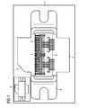
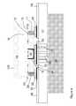
- FIG. 1For example, conventional power transistor package 1 is illustrated in FIG. 1 .
- Transistor 7 and capacitors 5are mounted on substrate 8 .
- Package 1contains metallic ground connection 2 , radio frequency (RF) output and direct current (DC) input 3 .
- Package 1also contains RF input 4 .
- Ceramic lid 6is placed over substrate 8 and tightly sealed to complete the package for power transistor 1 .
- a semiconductor devicein an embodiment, includes a semiconductor substrate.
- the semiconductor substratehas a first cavity disposed through it, and conductive material covers at least the bottom portion of the first cavity.
- An integrated circuitis disposed on the top surface of the conductive material.
- the devicefurther includes a cap disposed on the top surface of the substrate, such that a cavity disposed on a surface of the cap overlies the first cavity in the substrate.
- FIG. 1illustrates a prior art package of an LDMOS transistor
- FIGS. 2 a and 2 billustrate an IC package in accordance with an embodiment of the invention
- FIGS. 3 a - killustrate a method of packaging an IC in accordance with an embodiment of the invention
- FIGS. 4 a - billustrate an IC package in accordance with an embodiment of the invention
- FIG. 5illustrates an IC package in accordance with another embodiment of the invention
- FIG. 6illustrates an IC package in accordance with a further embodiment of the invention.
- FIG. 7illustrates a method of packaging an IC in accordance with an embodiment of the invention.
- Embodimentsinvolve providing a wafer on which passive components are fabricated. Recesses are etched in the wafer and lined with a conductive material. Integrated circuits, such as power transistor dice, are placed in the recesses on top of the conductive material. The integrated circuits are then bonded to the passive components by bond wires. Next, bond wires are attached to connect the passive components to input conductive material and to output conductive material. A cap is attached to the wafer over the integrated circuit and over the bond wires such that they are enclosed. Next, the bottom of the wafer is ground to expose the conductive material on the bottom of the wafer. Conductive pads are attached to the exposed bottom of the conductive material. After testing, the wafer is diced and finally assembled in a tape and reel.
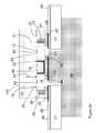
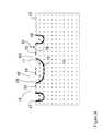
- FIGS. 2 a and 2 bAn embodiment of wafer level package 100 is illustrated in FIGS. 2 a and 2 b .
- FIG. 2 aillustrates a cross section illustrating the physical arrangement of elements
- FIG. 2 billustrates a schematic of the circuit.
- Substrate 10contains a layer of nonconductive material 13 . Disposed in nonconductive material 13 are capacitors 12 and 52 . In one embodiment, capacitors 12 and 52 are Metal-Insulator-Metal (MIM) capacitors.
- MIMMetal-Insulator-Metal
- Conductive material 15lines at least the bottom of cavity 14 . In one embodiment, conductive material 15 lines the entire inner surface of cavity 14 . Alternately, only the bottom part of cavity 14 is lined with conductive material 15 . The bottom of conductive material 15 extends to the bottom of substrate 10 .
- Integrated circuit 16is disposed on conductive material 15 . In one embodiment, integrated circuit 16 is and LDMOS power transistor. In other embodiments, integrated circuit 16 is another type of radio frequency (RF) transistor.
- RFradio frequency
- Substrate 10contains through silicon vias (TSV) 11 and 39 for interfacing with external circuits.
- Bond wire 18couples IC 16 and capacitor 52 .
- Bond wire 50couples IC 16 and capacitor 12 .
- Bond wire 51couples capacitor 12 to output TSV 11 .
- Bond wire 49couples capacitor 12 to input TSV 39 .
- Cap 19contains cavity 43 .
- Cap 19is disposed on the top surface of substrate 10 such that cavity 43 overlies cavity 14 .
- Metallic interconnect 20connects cap 19 to substrate 10 .
- Ground contact 23is coupled to conductive material 15 .
- Input contact 22is coupled to input TSV 39 .
- Output contact 24is coupled to output TSV 11 .
- Conductive material 25is coupled to input contact 22 .
- Conductive material 44is coupled to ground contact 23 .
- Conductive material 45is coupled to output contact 24 .
- Conductive materials 44 , 25 , 45 and 46are coupled to external heat sink 28 , conductive material 46 , conductive material 26 , and printed circuit board (PCB) 27 , respectively.
- PCB 27contains a hole that allows ground contact 23 , and therefore IC 16 , to be coupled to external heat sink 28 thermally and electrically.
- Conductive material 26is disposed on printed circuit board 27 .
- Printed circuit board 27is disposed on external heat sink 28 .
- FIG. 2 billustrates a schematic representation of the circuit for the embodiment illustrated in FIG. 2 a .
- Input (conductive material) 39is connected it inductor (bond wire) 18 .
- Inductor 18is connected to capacitor 15 , which is grounded, and to inductor (bond wire) 49 .
- Inductor 49is connected to the gate of transistor (IC) 16 .
- the source of transistor 16is connected to ground (conductive material) 15 .
- the drain of transistor 16is connected to inductor (bond wire) 50 .
- Inductor 50is connected to capacitor 12 , which is grounded, and to inductor (bond wire) 51 .
- Inductor 51is connected to output (conductive material) 11 .
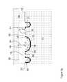
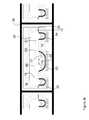
- FIGS. 3 a - 3 lillustrate cross sections representing an embodiment of wafer level packaging.
- FIG. 3 aillustrates substrate 10 , which is provided.
- substrate 10is a silion high ohmic substrate.
- substrate 10may be another type of semiconductor material, such as low ohmic substrate, SiC or glass wafer.
- substrate 10contains nonconductive material 13 at the top surface of substrate 10 .
- Nonconductive materialmay be, for example, CVD Oxide, TEOS, thermal Oxide, Bor Phoshporous Silicate glass, Silicon Nitride, Silicon Oxi-Nitride, and/or Polyimide.
- passive elementsare fabricated on substrate 10 using techniques known in the art.
- the passive elementscan include capacitors 12 and 52 and resistors.
- active devicescan also be fabricated on substrate 10 .
- the capacitorscan be Metal-Oxide-Metal (MIM) capacitors, poly-poly capacitors, sandwich capacitors, metal oxide semiconductor (MOS) capacitors, or other capacitor types.
- Resistorscan include, for example polysilicon resistors or metal line resistors.
- recesses 29 , 30 and 31are etched in substrate 10 .
- recesses 29 , 30 and 31are etched using an isotropic etch, such as reactive ion etching (RIE), plasma etching, vapor phase etching, or wet etching.
- recesses 29 , 30 and 31are etched using an anisotropic etch.
- Embodiment anisotropic etching processesinclude sputter etching, RIE etching, plasma etching or wet etching.
- Recesses 29 , 30 and 31have a height 40 . In some embodiments, height 40 is between about 50 microns to about 100 microns.
- conductive material 15 , 47 and 48is deposited in at least the bottom portions of recesses 29 , 30 and 31 .
- the depositionis performed by a copper galvanic process, sputtering, or another process.
- Conductive material 15 , 47 and 48has thickness 32 of between about 10 microns and about 40 microns.
- conductive material 15 , 47 and 48is copper, aluminum, gold or another conductive material.
- IC 16is attached to conductive material 15 .
- the attachingis performed by diffusion soldering, eutectic bonding, galvanic connection, metallically conductive paste, gluing, or other methods of attaching.
- FIG. 3 eshows the optional step of at least partially filling recesses 29 , 30 and 31 with embedding material 17 .
- the embedding processincludes performing a thermoplastic process, refilling with a non-conductive paste, or using other methods of filling with embedding.
- the embedding materialis underfiller, globe top, epoxy, silicone, imide or thermoplast.
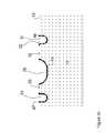
- bond wiresare attached.
- Bond wire 49is attached to IC 16 and to capacitor 52
- bond wire 18is attached to capacitor 52 and to conductive material 47
- bond wire 50is attached to IC 16 and to capacitor 12
- bond wire 51is attached to capacitor 12 and conductive material 48 .
- Bond wires 18 , 49 , 50 and 51have a height 35 . In some embodiments, height 35 is between about 100 microns to about 200 microns. Alternately, other heights can be used.
- the inductances of bond wires 18 , 49 , 50 and 51are tuned to impedance match the input and output to optimize performance.
- cap 19 containing recess 33is bonded to substrate 10 using connecting material 20 .
- Recess 33is etched in cap 19 .
- recess 33is formed by isotropic etching.
- recess 33is formed by anisotropic etching.
- the bondingis performed by wafer bonding, diffusion bonding, or another bonding method. The bonding is performed at the wafer level.
- cap 19is thermally matched to substrate 10 .
- cap 19is the same material as substrate 10 .
- cap 19is a low ohmic material.
- cap 19is silicon, glass, silicon coated with a conductive material, metal, or another material. Alternatively, single metal lids may be used.
- Recess 33is placed over IC 16 and bond wires 18 , 49 , 50 and 51 .
- the height 34 of recess 19is about twice the height 35 of bond wires 18 , 49 , 50 , and 51 .
- height 34is between about 200 microns to about 400 microns.
- connecting material 20is floating. In other embodiments, connecting material 20 is grounded.
- connecting material 20is a nonconductive material such as epoxy or silicone glue. In other embodiments, connecting material 20 is a conductive material such as solder or conductive glue.
- substrate 10is ground or thinned such that bottom 36 conductive material 15 is exposed at the bottom 21 of substrate 10 .
- the grindingis performed by chemical mechanical polishing (CMP).
- CMPchemical mechanical polishing
- substrate 10has a thickness 41 .
- thickness 41is between about 100 microns to about 400 microns. However, other thicknesses can be used in alternative embodiments.
- conductive pad 23is attached to conductive material 15
- conductive pad 22is attached to conductive material 47
- conductive pad 24is attached to conductive material 48 .
- the attachingis performed by printing solder paste, by sputtering, or by another method.
- conductive pads 22 , 23 and 24are made of gold, tin, copper, tin, or multi metal stacks, such as NiP/Pd/Au, ENIG (electroless deposited galvanic Ni Au). In further embodiments or another conductive material may be used.
- the waferis diced at scribe line 37 .
- dicingis performed using techniques known in the art, for example sawing.
- a final testis performed.
- the diced waferis placed on tape and reel 38 for distribution to the final customer.
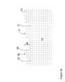
- FIGS. 4 a and 4 bshow an alternate embodiment for a matching circuit.
- FIG. 4 ashows a cross section illustrating the physical arrangement of elements
- FIG. 4 bshows a circuit diagram of the matching circuit.
- Input (conductive material) 47is connected to inductor (bond wire) 53 .
- Inductor 53is connected to capacitor 52 , which is grounded.
- Inductor 53is also connected to inductor (bond wire) 49 , which is connected to the gate of transistor (IC) 16 .
- the source of transistor 16is connected to ground (conductive material) 15 .
- the drain of transistor 16is connected to inductor (bond wire) 50 and to inductor (bond wire) 54 .
- Inductor 50is connected to capacitor 12 , which is grounded.
- Inductor 54is connected to output (conductive material) 48 .
- FIG. 5An alternative embodiment of wafer level package 100 is illustrated in FIG. 5 .
- the embodiment illustrated in FIG. 5is similar to the embodiment illustrated in FIG. 3 i except for the following differences.
- the embodiment illustrated in FIG. 5does not have embedding material in recess 14 .
- Recess 30with embedding material 17 and conductive material 47 , in the embodiment illustrated in FIG. 3 i , is replaced with TSV 36 in the embodiment illustrated in FIG. 5 .
- recess 31with embedding material 17 and conductive material 48 , in the embodiment illustrated in FIG. 3 i , is replaced with TSV 11 in FIG. 5 .
- FIG. 6A further alternative embodiment of wafer level package 100 is illustrated in FIG. 6 .
- the embodiment illustrated in FIG. 6is similar to the embodiment illustrated in FIG. 2 a except for the following differences.
- the coupling of conductive material 15 and IC 16 with external heat sink 28is performed by ground contact 23 contacting conductive material 44 , which contacts PCB 27 .
- PCB 27contains vias 42 , which contact both conductive material 44 and external heat sink 28 , providing a thermal and electrical coupling.
- external heat sinkis thermally coupled to IC 16 via conductive material 16 , contacting conductive material 44 , conductive material 55 , ground contact 23 and vias within PCB 27 .
- FIG. 7shows an embodiment of a method of packaging an IC.
- Step 200involves providing a substrate that contains passive elements.
- step 202is etching recesses in the substrate, followed by step 204 , depositing conductive material in at least the bottom of the recesses.
- Step 206is attaching an IC to the conductive material in a recess.
- Step 208an optional step, involves at least partially filling the recesses with embedding material.
- testing step 210is performed.
- Testing step 210involves testing a send ahead wafer to optimize impedance matching by adjusting the inductance of bond wires by adjusting the length of the bond wires.
- bond wiresare attached in step 212 .
- a capis bonded to the substrate in step 214 , and the bottom of the wafer is ground in step 216 , such that the bottom of the conductive material is exposed at the bottom of the wafer.
- conductive padsare attached to the bottom of the conductive material at the bottom of the wafer.
- Advantages of embodimentsinclude a low cost of packaging. Because the packaging is performed at the wafer level, many ICs can be packaged simultaneously at a low cost. Bond wire lengths can be tuned to create a matching circuit for multiple ICs at the same time, further contributing to a low cost. Advantages of embodiments also include that the bond wires are surrounded by air, which reduces coupling. Shorter bond wire lengths reduce packaging parasitic coupling. The structure of an IC in a cavity provides good thermal coupling to the heat sink.
Landscapes
- Engineering & Computer Science (AREA)
- Microelectronics & Electronic Packaging (AREA)
- Physics & Mathematics (AREA)
- Condensed Matter Physics & Semiconductors (AREA)
- General Physics & Mathematics (AREA)
- Computer Hardware Design (AREA)
- Power Engineering (AREA)
- Internal Circuitry In Semiconductor Integrated Circuit Devices (AREA)
- Semiconductor Integrated Circuits (AREA)
Abstract
Description
Claims (31)
Priority Applications (3)
| Application Number | Priority Date | Filing Date | Title |
|---|---|---|---|
| US13/183,272US8497558B2 (en) | 2011-07-14 | 2011-07-14 | System and method for wafer level packaging |
| EP12176354.4AEP2546876B1 (en) | 2011-07-14 | 2012-07-13 | System and method for wafer level packaging |
| CN201210242319.6ACN102881665B (en) | 2011-07-14 | 2012-07-13 | System and method for wafer level packaging |
Applications Claiming Priority (1)
| Application Number | Priority Date | Filing Date | Title |
|---|---|---|---|
| US13/183,272US8497558B2 (en) | 2011-07-14 | 2011-07-14 | System and method for wafer level packaging |
Publications (2)
| Publication Number | Publication Date |
|---|---|
| US20130015467A1 US20130015467A1 (en) | 2013-01-17 |
| US8497558B2true US8497558B2 (en) | 2013-07-30 |
Family
ID=46516577
Family Applications (1)
| Application Number | Title | Priority Date | Filing Date |
|---|---|---|---|
| US13/183,272Active2031-07-16US8497558B2 (en) | 2011-07-14 | 2011-07-14 | System and method for wafer level packaging |
Country Status (3)
| Country | Link |
|---|---|
| US (1) | US8497558B2 (en) |
| EP (1) | EP2546876B1 (en) |
| CN (1) | CN102881665B (en) |
Cited By (1)
| Publication number | Priority date | Publication date | Assignee | Title |
|---|---|---|---|---|
| US9952111B2 (en) | 2015-04-15 | 2018-04-24 | Infineon Technologies Ag | System and method for a packaged MEMS device |
Families Citing this family (22)
| Publication number | Priority date | Publication date | Assignee | Title |
|---|---|---|---|---|
| US9355997B2 (en) | 2014-03-12 | 2016-05-31 | Invensas Corporation | Integrated circuit assemblies with reinforcement frames, and methods of manufacture |
| US20150262902A1 (en) | 2014-03-12 | 2015-09-17 | Invensas Corporation | Integrated circuits protected by substrates with cavities, and methods of manufacture |
| US9165793B1 (en) | 2014-05-02 | 2015-10-20 | Invensas Corporation | Making electrical components in handle wafers of integrated circuit packages |
| EP3140838B1 (en) | 2014-05-05 | 2021-08-25 | 3D Glass Solutions, Inc. | Inductive device in a photo-definable glass structure |
| US9741649B2 (en) | 2014-06-04 | 2017-08-22 | Invensas Corporation | Integrated interposer solutions for 2D and 3D IC packaging |
| US9412806B2 (en) | 2014-06-13 | 2016-08-09 | Invensas Corporation | Making multilayer 3D capacitors using arrays of upstanding rods or ridges |
| US9252127B1 (en) | 2014-07-10 | 2016-02-02 | Invensas Corporation | Microelectronic assemblies with integrated circuits and interposers with cavities, and methods of manufacture |
| CN104697700B (en)* | 2015-02-06 | 2017-07-14 | 北京大学 | A kind of piezoresistive pressure gage chip structure and preparation method thereof |
| US9478504B1 (en) | 2015-06-19 | 2016-10-25 | Invensas Corporation | Microelectronic assemblies with cavities, and methods of fabrication |
| US12165809B2 (en) | 2016-02-25 | 2024-12-10 | 3D Glass Solutions, Inc. | 3D capacitor and capacitor array fabricating photoactive substrates |
| JP7008824B2 (en) | 2017-12-15 | 2022-01-25 | スリーディー グラス ソリューションズ,インク | Connection transmission line resonant RF filter |
| EP3735743A4 (en) | 2018-01-04 | 2021-03-03 | 3D Glass Solutions, Inc. | Impedance matching conductive structure for high efficiency rf circuits |
| US11894322B2 (en) | 2018-05-29 | 2024-02-06 | Analog Devices, Inc. | Launch structures for radio frequency integrated device packages |
| US11424196B2 (en) | 2018-06-01 | 2022-08-23 | Analog Devices, Inc. | Matching circuit for integrated circuit die |
| US11417615B2 (en)* | 2018-11-27 | 2022-08-16 | Analog Devices, Inc. | Transition circuitry for integrated circuit die |
| AU2019416325A1 (en) | 2018-12-28 | 2021-02-04 | 3D Glass Solutions, Inc. | Heterogenous integration for RF, microwave and mm wave systems in photoactive glass substrates |
| JP7140435B2 (en) | 2019-04-05 | 2022-09-21 | スリーディー グラス ソリューションズ,インク | Glass-based empty substrate integrated waveguide device |
| KR102601781B1 (en) | 2019-04-18 | 2023-11-14 | 3디 글래스 솔루션즈 인코포레이티드 | High efficiency die dicing and release |
| KR20220164800A (en) | 2020-04-17 | 2022-12-13 | 3디 글래스 솔루션즈 인코포레이티드 | broadband inductor |
| DE102020110896B4 (en)* | 2020-04-22 | 2025-07-17 | Infineon Technologies Ag | Electronic component comprising a semiconductor chip having a low-resistance part with an active region and a high-resistance part on a dielectric layer |
| US11744021B2 (en) | 2022-01-21 | 2023-08-29 | Analog Devices, Inc. | Electronic assembly |
| US20250079192A1 (en)* | 2023-09-01 | 2025-03-06 | Applied Materials, Inc. | Modular Fluid Delivery Assembly |
Citations (12)
| Publication number | Priority date | Publication date | Assignee | Title |
|---|---|---|---|---|
| US6271607B1 (en) | 1998-06-26 | 2001-08-07 | Valeo Equipments Electriques Moteur | Sub-assemblies with electronic components, for motor vehicle alternators |
| US6635509B1 (en)* | 2002-04-12 | 2003-10-21 | Dalsa Semiconductor Inc. | Wafer-level MEMS packaging |
| EP1394857A2 (en) | 2002-08-28 | 2004-03-03 | Matsushita Electric Industrial Co., Ltd. | Semiconductor device |
| US20040080044A1 (en) | 2001-02-06 | 2004-04-29 | Shinji Moriyama | Hybrid integrated circuit device and method for fabricating the same and electronic device |
| US20060113598A1 (en)* | 2004-11-16 | 2006-06-01 | Chen Howard H | Device and method for fabricating double-sided SOI wafer scale package with optical through via connections |
| US20070134336A1 (en)* | 2003-08-04 | 2007-06-14 | Camurus Ab | Method for improving the properties of amphiphile particles |
| US20070275300A1 (en)* | 2006-05-24 | 2007-11-29 | Commissariat A L'energie Atomique | Integrated microcomponent combining energy recovery and storage functions |
| US20080190748A1 (en)* | 2007-02-13 | 2008-08-14 | Stephen Daley Arthur | Power overlay structure for mems devices and method for making power overlay structure for mems devices |
| US20100044853A1 (en)* | 2007-01-17 | 2010-02-25 | Nxp, B.V. | System-in-package with through substrate via holes |
| US20100096713A1 (en)* | 2006-12-07 | 2010-04-22 | Electronic And Telecommunications Research Institute | Mems package and packaging method thereof |
| US20120080701A1 (en)* | 2008-11-25 | 2012-04-05 | Wan Ho Kim | Light emitting device package |
| US8151640B1 (en)* | 2008-02-05 | 2012-04-10 | Hrl Laboratories, Llc | MEMS on-chip inertial navigation system with error correction |
Family Cites Families (3)
| Publication number | Priority date | Publication date | Assignee | Title |
|---|---|---|---|---|
| KR100497111B1 (en)* | 2003-03-25 | 2005-06-28 | 삼성전자주식회사 | WL CSP, stack package stacking the same and manufacturing method thereof |
| US7446407B2 (en)* | 2005-08-31 | 2008-11-04 | Chipmos Technologies Inc. | Chip package structure |
| KR20150068495A (en)* | 2007-11-30 | 2015-06-19 | 스카이워크스 솔루션즈, 인코포레이티드 | Wafer level packaging using flip chip mounting |
- 2011
- 2011-07-14USUS13/183,272patent/US8497558B2/enactiveActive
- 2012
- 2012-07-13EPEP12176354.4Apatent/EP2546876B1/enactiveActive
- 2012-07-13CNCN201210242319.6Apatent/CN102881665B/enactiveActive
Patent Citations (12)
| Publication number | Priority date | Publication date | Assignee | Title |
|---|---|---|---|---|
| US6271607B1 (en) | 1998-06-26 | 2001-08-07 | Valeo Equipments Electriques Moteur | Sub-assemblies with electronic components, for motor vehicle alternators |
| US20040080044A1 (en) | 2001-02-06 | 2004-04-29 | Shinji Moriyama | Hybrid integrated circuit device and method for fabricating the same and electronic device |
| US6635509B1 (en)* | 2002-04-12 | 2003-10-21 | Dalsa Semiconductor Inc. | Wafer-level MEMS packaging |
| EP1394857A2 (en) | 2002-08-28 | 2004-03-03 | Matsushita Electric Industrial Co., Ltd. | Semiconductor device |
| US20070134336A1 (en)* | 2003-08-04 | 2007-06-14 | Camurus Ab | Method for improving the properties of amphiphile particles |
| US20060113598A1 (en)* | 2004-11-16 | 2006-06-01 | Chen Howard H | Device and method for fabricating double-sided SOI wafer scale package with optical through via connections |
| US20070275300A1 (en)* | 2006-05-24 | 2007-11-29 | Commissariat A L'energie Atomique | Integrated microcomponent combining energy recovery and storage functions |
| US20100096713A1 (en)* | 2006-12-07 | 2010-04-22 | Electronic And Telecommunications Research Institute | Mems package and packaging method thereof |
| US20100044853A1 (en)* | 2007-01-17 | 2010-02-25 | Nxp, B.V. | System-in-package with through substrate via holes |
| US20080190748A1 (en)* | 2007-02-13 | 2008-08-14 | Stephen Daley Arthur | Power overlay structure for mems devices and method for making power overlay structure for mems devices |
| US8151640B1 (en)* | 2008-02-05 | 2012-04-10 | Hrl Laboratories, Llc | MEMS on-chip inertial navigation system with error correction |
| US20120080701A1 (en)* | 2008-11-25 | 2012-04-05 | Wan Ho Kim | Light emitting device package |
Cited By (1)
| Publication number | Priority date | Publication date | Assignee | Title |
|---|---|---|---|---|
| US9952111B2 (en) | 2015-04-15 | 2018-04-24 | Infineon Technologies Ag | System and method for a packaged MEMS device |
Also Published As
| Publication number | Publication date |
|---|---|
| US20130015467A1 (en) | 2013-01-17 |
| EP2546876B1 (en) | 2019-05-15 |
| CN102881665A (en) | 2013-01-16 |
| CN102881665B (en) | 2015-06-03 |
| EP2546876A1 (en) | 2013-01-16 |
Similar Documents
| Publication | Publication Date | Title |
|---|---|---|
| US8497558B2 (en) | System and method for wafer level packaging | |
| US8154134B2 (en) | Packaged electronic devices with face-up die having TSV connection to leads and die pad | |
| US6867492B2 (en) | Radio-frequency power component, radio-frequency power module, method for producing a radio-frequency power component, and method for producing a radio-frequency power module | |
| US9443828B2 (en) | Semiconductor device and method of embedding thermally conductive layer in interconnect structure for heat dissipation | |
| JP5129939B2 (en) | Manufacturing method of semiconductor device | |
| US12125799B2 (en) | Embedded die packaging with integrated ceramic substrate | |
| US20050101116A1 (en) | Integrated circuit device and the manufacturing method thereof | |
| US20090261476A1 (en) | Semiconductor device and manufacturing method thereof | |
| US20070023886A1 (en) | Method for producing a chip arrangement, a chip arrangement and a multichip device | |
| US20230099787A1 (en) | Semiconductor package and method of fabricating the same | |
| US20080283971A1 (en) | Semiconductor Device and Its Fabrication Method | |
| US20200235067A1 (en) | Electronic device flip chip package with exposed clip | |
| US9165792B2 (en) | Integrated circuit, a chip package and a method for manufacturing an integrated circuit | |
| CN101305464A (en) | Chip assembly and method of manufacturing the same | |
| US10593615B2 (en) | Chip package with sidewall metallization | |
| WO2009088069A1 (en) | Manufacturing method for condenser-packaged device, and manufacturing method for condenser-packaged package | |
| KR100577527B1 (en) | High frequency device and its manufacturing method | |
| US9153510B2 (en) | Semiconductor device and method of manufacturing the same | |
| US20240404996A1 (en) | Package with vertically stacked devices, and fabrication methods thereof | |
| US20100105168A1 (en) | Microelecronic assembly and method for forming the same | |
| US20040089930A1 (en) | Simplified stacked chip assemblies | |
| JP2006173474A (en) | Semiconductor device and manufacturing method thereof | |
| WO2019163580A1 (en) | Semiconductor device and method for manufacturing semiconductor device |
Legal Events
| Date | Code | Title | Description |
|---|---|---|---|
| AS | Assignment | Owner name:INFINEON TECHNOLOGIES AG, GERMANY Free format text:ASSIGNMENT OF ASSIGNORS INTEREST;ASSIGNORS:KRUMBEIN, ULRICH;LOHNINGER, GERHARD;DEHE, ALFONS;SIGNING DATES FROM 20110712 TO 20110713;REEL/FRAME:026593/0890 | |
| FEPP | Fee payment procedure | Free format text:PAYOR NUMBER ASSIGNED (ORIGINAL EVENT CODE: ASPN); ENTITY STATUS OF PATENT OWNER: LARGE ENTITY | |
| STCF | Information on status: patent grant | Free format text:PATENTED CASE | |
| FPAY | Fee payment | Year of fee payment:4 | |
| AS | Assignment | Owner name:CREE, INC., NORTH CAROLINA Free format text:ASSIGNMENT OF ASSIGNORS INTEREST;ASSIGNOR:INFINEON TECHNOLOGIES AG;REEL/FRAME:045870/0504 Effective date:20180306 | |
| MAFP | Maintenance fee payment | Free format text:PAYMENT OF MAINTENANCE FEE, 8TH YEAR, LARGE ENTITY (ORIGINAL EVENT CODE: M1552); ENTITY STATUS OF PATENT OWNER: LARGE ENTITY Year of fee payment:8 | |
| AS | Assignment | Owner name:U.S. BANK TRUST COMPANY, NATIONAL ASSOCIATION, NORTH CAROLINA Free format text:SECURITY INTEREST;ASSIGNOR:WOLFSPEED, INC.;REEL/FRAME:064185/0755 Effective date:20230623 | |
| MAFP | Maintenance fee payment | Free format text:PAYMENT OF MAINTENANCE FEE, 12TH YEAR, LARGE ENTITY (ORIGINAL EVENT CODE: M1553); ENTITY STATUS OF PATENT OWNER: LARGE ENTITY Year of fee payment:12 |