US8494030B2 - Method and system for 60 GHz wireless clock distribution - Google Patents
Method and system for 60 GHz wireless clock distributionDownload PDFInfo
- Publication number
- US8494030B2 US8494030B2US12/192,653US19265308AUS8494030B2US 8494030 B2US8494030 B2US 8494030B2US 19265308 AUS19265308 AUS 19265308AUS 8494030 B2US8494030 B2US 8494030B2
- Authority
- US
- United States
- Prior art keywords
- chip
- wireless
- antenna array
- relay
- wireless link
- Prior art date
- Legal status (The legal status is an assumption and is not a legal conclusion. Google has not performed a legal analysis and makes no representation as to the accuracy of the status listed.)
- Expired - Fee Related, expires
Links
Images


Classifications
- H—ELECTRICITY
- H04—ELECTRIC COMMUNICATION TECHNIQUE
- H04L—TRANSMISSION OF DIGITAL INFORMATION, e.g. TELEGRAPHIC COMMUNICATION
- H04L7/00—Arrangements for synchronising receiver with transmitter
- H04L7/0008—Synchronisation information channels, e.g. clock distribution lines
- H—ELECTRICITY
- H04—ELECTRIC COMMUNICATION TECHNIQUE
- H04W—WIRELESS COMMUNICATION NETWORKS
- H04W56/00—Synchronisation arrangements
Definitions
- Certain embodiments of the inventionrelate to communication systems. More specifically, certain embodiments of the invention relate to a method and system for 60 GHz wireless clock distribution.
- a method and/or system for 60 GHz wireless clock distributionsubstantially as shown in and/or described in connection with at least one of the figures, as set forth more completely in the claims.
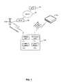
- FIG. 1is a diagram illustrating an exemplary wireless communication system, in accordance with an embodiment of the invention.
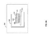
- FIG. 2Ais a diagram illustrating an exemplary chip-based antenna array, in accordance with an embodiment of the invention.
- FIG. 2Bis a diagram of a 60 GHz inter-chip wireless clock distribution system, in accordance with an embodiment of the invention.
- FIG. 2Cis a diagram of a 60 GHz inter-chip wireless clock distribution system, in accordance with an embodiment of the invention.
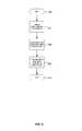
- FIG. 3is a flow chart illustrating an exemplary wireless clock distribution setup, in accordance with an embodiment of the invention.
- Certain embodiments of the inventionmay be found in a method and system for 60 GHz wireless clock distribution.
- Aspects of a method and system for 60 GHz wireless clock distributionmay comprise configuring a microwave communication link established between a first chip and a second chip via a wireline communication bus.
- the configurationmay comprise adjusting beamforming parameters of a first antenna array communicatively coupled to the first chip, and a second antenna array communicatively coupled to the second chip.
- the first chip and the second chipmay communicate a clock signal via the microwave communication link.
- the microwave communication linkmay be routed via one or more relay chips in instances when the first chip and the second chip cannot directly communicate with each other. Control data may be transferred between the first chip, the second chip, and/or the one or more relay chips, which may comprise one or more antennas.
- the relay chipsmay be dedicated relay ICs or multi-purpose transmitter/receivers.
- the first chip and the second chipmay be operable to receive and transmit in the 60 GHz frequency band.
- the first antenna array and/or the second antenna arraymay be on an integrated circuit package, or on an integrated circuit of the first chip and/or the second chip, respectively.
- the first antenna array and the second antenna arraymay comprise one or more antennas.
- the beamforming parametersmay be adjusted to optimize one or more wireless clock distribution performance metrics.
- FIG. 1is a diagram illustrating an exemplary wireless communication system, in accordance with an embodiment of the invention.
- an access point 112 bthere is shown an access point 112 b , a computer 110 a , a portable storage 114 a , a router 130 , the Internet 132 and a web server 134 .
- the computer or host device 110 amay comprise a wireless radio 111 a , a short-range radio 111 b , a host processor 111 c , and a host memory 111 d .
- There is also shown a wireless connection between the wireless radio 111 a and the access point 112 bThere is also shown a wireless connection between the wireless radio 111 a and the access point 112 b , and a short-range wireless connection between the short-range radio 111 b and the portable storage 114 a.
- the access point 112 bmay comprise suitable logic, circuitry and/or code that may be enabled to transmit and receive radio frequency signals for data communications, for example with the wireless radio 111 a .
- the access point 112 bmay also be enabled to communicate via a wired network, for example, with the router 130 .
- the wireless radio 111 amay comprise suitable logic, circuitry and/or code that may enable communications over radio frequency waves with one or more other radio communication devices.
- the wireless radio 111 a and the access point 112 bmay be compliant with one or more mobile communication standard, for example, GSM, UMTS, and CDMA2000.
- the short range radio 111 bmay comprise suitable logic, circuitry and/or code that may enable communications over radio frequencies with one or more other communication devices, for example the portable storage 114 a .
- the short range radio 111 b and/or the portable storage 114 amay be compliant with a wireless industry standard, for example Bluetooth, and IEEE 802.11 Wireless LAN.
- the host processor 111 cmay comprise suitable logic, circuitry and/or code that may be enabled to generate and process data.
- the host memory 111 dmay comprise suitable logic, circuitry and/or code that may be enabled to store and retrieve data for various system components and functions of the computer 110 a .
- the router 130may comprise suitable logic, circuitry and/or code that may be enabled to communicate with communication devices that may be communicatively coupled to it, for example access point 112 b or the Internet 132 .
- the Internet 132may comprise various devices comprising suitable logic, circuitry and/or code that may be enabled to interconnect and exchange data between a plurality of communication devices.
- the web server 134may comprise suitable logic, circuitry and/or code that may be enabled to communicate with communication devices that may be communicatively coupled to it, for example the Internet 132 .
- computing and communication devicesmay comprise hardware and/or software that may enable communication using multiple wireless communication standards and/or protocols.
- the wireless radio 111 a and the short-range radio 111 bmay be active concurrently.
- the usermay establish a wireless connection between the computer 110 a and the access point 112 b . Once this connection is established, the streaming content from the Web server 134 may be received via the router 130 , the access point 112 b , and the wireless connection, and consumed by the computer or host device 110 a.
- the user of the computer 110 amay establish a short-range wireless connection with the portable storage 114 a .
- a wireless connection between the portable storage 114 a and the computer 110 amay be using a Bluetooth, IEEE 802.11 Wireless LAN, Ultrawideband, or 60 GHz communications protocol.
- the short-range wireless connectionis established, and with suitable configurations on the computer 110 a enabled, data may be transferred from/to the portable storage 114 a .
- the data link between the portable storage 114 a and the computer 110 amay be enabled for high data rates.
- high data ratesmay require high frequency clocks at, for example, the components comprised in the computer 110 a .
- High frequency clocksmay cause distribution problems due to undesirable clock leakage into circuitry and/or losses associated with wireline distribution, for example attenuation losses and transmission line behavior of conductors.
- itmay be desirable to distribute the clock wirelessly.
- FIG. 2Ais a diagram illustrating an exemplary chip-based antenna array, in accordance with an embodiment of the invention.
- a device 202may comprise a casing 204 , one or more printed circuit boards (PCBs) 214 , and one or more integrated circuits (ICs, chip), of which IC 212 may be illustrated.
- the IC 212may comprise one or more antennas, of which antennas 206 , 208 and 210 may be illustrated.
- the device 202may be, for example, a portable storage device.
- the IC 212may comprise suitable logic, circuitry and/or code that may be enabled to generate and/or process radio frequency signals for reception and/or transmission via the one or more antennas, of which antennas 206 , 208 and 210 may be illustrated.
- the antennas 206 , 208 , and 210may be used together to form an antenna array.
- the antennas 206 , 208 and 210may be implemented on the package of the IC 212 and/or directly on the IC 212 . In these instances, the chip package may be constructed from radio-wave permeable materials, for example.
- a plurality of chips similar to chip 212 illustrated in FIG. 2Amay communicate together at high data rates via, for example, 60 GHz wireless links via antenna arrays that may be implemented on and/or in the chip as described above.
- one or more communication linksmay be established between, for example, IC 212 and other chips associated to the device 202 .
- the antenna arraycomprising antennas 206 , 208 , and 210 , for example, on the device 202 , and the antenna array on a communicating IC may be enabled to automatically steer the transmission and/or reception beam in a direction that may optimize the signal quality and hence the data rates that may be achievable.
- FIG. 2Bis a diagram of a 60 GHz inter-chip wireless clock distribution system, in accordance with an embodiment of the invention. Referring to FIG. 2B , there is shown a wireline communication bus 238 , ICs 220 , 222 , 226 , 228 , 230 , 234 , and 236 .
- the ICs 220 , 222 , 226 , 228 , 230 , 234 , and 236may be substantially similar.
- each of the ICs 220 , 222 , 226 , 228 , 230 , 234 , and 236may comprise an antenna array 220 a , 222 a , 226 a , 228 a , 230 a , 234 a , and 236 a , respectively.
- the IC 220may comprise suitable logic, circuitry and/or code that may be enabled to communicate on radio-frequency frequencies via the antenna array 220 a , and via the wireline communication bus 238 .
- relay ICs 224 and 232There is also shown relay ICs 224 and 232 .
- the relay ICs 224 and 232may be substantially similar.
- the ICs 224 and 232may comprise one or more antenna arrays.
- IC 224may comprise an antenna array 224 a and an antenna array 224 b .
- the relay IC 232may comprise antenna arrays 232 a and 232 b , for example.
- the relay IC 232may comprise suitable logic, circuitry and/or code that may be enabled to communicate a clock signal on radio frequencies via the antenna arrays 224 a and 224 b , and via wireline communication via the wireline communication bus 238 .
- the ICs 220 , 222 , 226 , 228 , 230 , 234 , and 236 and the relay ICs 224 and 232may be communicatively coupled to the wireline bus 238 .
- one or more of the ICs 220 , 222 , 226 , 228 , 230 , 234 , 236 , and/or the relay ICs 224 and 232may enable the processing of any form of signals such as, for example, multimedia information, comprising, audio, video, and/or data. Audio may comprise voice, any form of music and/or any form of sound.
- the processing of signals by the ICs 220 , 222 , 226 , 228 , 230 , 234 , 236 , and/or the relay ICs 224 and 232may occur in analog and/or digital format.
- the wireline bus 238may be utilized as a low rate communication bus and as a control signal transport media that may help establish a 60 GHz wireless clock distribution system between a plurality of ICs. For example, it may be desirable for the IC 220 to communicate with the IC 226 . Via the wireline bus 238 , the IC 220 and/or the IC 226 may initiate a communication session and parameters for a wireless radio connection may be exchanged. When a communication setup phase may be completed, the antenna array 220 a on IC 220 may be directed toward the antenna array 226 a on IC 226 , and a clock signal may be distributed wirelessly. In some instances, one or more ICs may not be able to directly communicate with another IC. For example, it may be desirable for the IC 220 to communicate with the IC 236 .
- the IC 236may not be in a line of sight of the IC 220 a because the IC 226 and the relay IC 232 , may be obstructing a direct wireless link from IC 220 to IC 236 .
- the wireless clock signalmay be routed via relay ICs.
- the relay ICsfor example the ICs 224 and 232 may be enabled to receive a wireless clock signal from one chip and forward it to another chip.
- the IC 220may transmit to the IC 236 via the relay IC 224 .
- the IC 220may communicate with the IC 236 via the relay IC 224 and the IC 232 .
- the IC 222may communicate with the IC 234 via the relay IC 232 , for example.
- the wireline bus 238may be utilized to exchange control information and/or wireless link setup information.
- FIG. 2Cis a diagram of a 60 GHz inter-chip wireless clock distribution system, in accordance with an embodiment of the invention.
- a wireline communication bus 270ICs 240 , 242 , 244 , 246 , 248 , 250 , 252 , 254 , 256 , 258 , 260 and 262 .
- the ICs 240 , 242 , 244 , 246 , 248 , 250 , 252 , 254 , 256 , 258 , 260 and 262may be substantially similar.
- each of the ICs 240 , 242 , 244 , 246 , 248 , 250 , 252 , 254 , 256 , 258 , 260 and 262may comprise an antenna array 240 a , 242 a , 244 a , 246 a , 248 a , 250 a , 252 a , 254 a , 256 a , 258 a , 260 a and 262 a , respectively.
- the IC 240may comprise suitable logic, circuitry and/or code that may be enabled to communicate on radio-frequency frequencies via the antenna array 240 a , and via the wireline communication bus 270 .
- the relay ICs 264 , 266 , and 268may be substantially similar to IC 240 .
- the relay ICs 264 , 266 , and 268may comprise one or more antenna arrays.
- relay IC 264may comprise an antenna array 264 a .
- the relay IC 264may comprise suitable logic, circuitry and/or code that may be enabled to communicate on radio-frequency frequencies via the antenna arrays 264 a , and via wireline communication via the wireline communication bus 270 .
- the ICs 240 , 242 , 244 , 246 , 248 , 250 , 252 , 254 , 256 , 258 , 260 and 262 and the relay ICs 264 , 266 , and 268may be communicatively coupled to the wireline communication bus 270 .
- the wireline communication bus 270may be used to exchange control information and setup a 60 GHz wireless clock distribution between a plurality of ICs.
- a regular grid of ICs as illustrated in FIG. 2Cmay be utilized.
- various embodiments of the inventionmay comprise a high density of chips since fewer physical connections may be required, for example, on the printed circuit board.
- the communication parametersmay be exchanged via the wireline communication bus 270 , and a wireless clock signal distribution may be initialized. In this instance, the IC 256 may steer its antenna array 256 a toward the relay IC 264 .
- the relay IC 264may relay a wireless clock signal from the IC 256 via the relay IC 266 and/or the relay IC 268 .
- the relay ICsmay be dedicated relay chips and/or multi-purpose transmitter/receiver chips that may be enabled to initiate wireless clock distribution on their own.
- FIG. 3is a flow chart illustrating an exemplary wireless clock distribution setup, in accordance with an embodiment of the invention.
- the setup processmay be initialized in step 302 .
- the initial wireless clock distribution setupmay be established, for example between the IC 250 and the IC 254 , as illustrated in FIG. 2C .
- the initialization of the communicationmay be achieved via a wireline bus, for example the wireline communication bus 270 , as described for FIG. 2B and FIG. 2C .
- the 60 GHz antenna arrays on the ICfor example IC 250 , may automatically and/or dynamically adjust their beam patterns in order to optimize some wireless clock distribution performance parameters.
- the beamsmay be adjusted in order to optimize signal strength.
- the transmission and reception of the wireless clock signal through the antenna arraysmay take place.
- a plurality of communicating ICsmay be required to transmit and/or receive data via relay ICs, for example relay ICs 264 , 266 , and 268 .
- a method and system for 60 GHz wireless clock distributionmay comprise configuring a microwave communication link established between a first chip, for example chip 222 , and a second chip, for example 234 , via a wireline communication bus 238 .
- the configurationmay comprise adjusting beamforming parameters of a first antenna array, for example 222 a , communicatively coupled to the first chip 222 , and a second antenna array, for example 234 a , communicatively coupled to the second chip 234 .
- the first chip, for example chip 222 , and the second chip, for example chip 234may communicate a clock signal via said microwave communication link, as described in FIG. 2B and FIG. 2C .
- the microwave communication linkmay be routed via one or more relay chips, for example relay chip 232 , when the first chip, for example chip 222 , and the second chip, for example chip 234 , cannot directly communicate.
- Control datamay be transferred between the first chip 222 , the second chip 234 , and/or the one or more relay chips, for example relay chip 232 , which may comprise one or more antennas, for example antennas 232 a and 232 b .
- the relay chipsmay be dedicated relay ICs or multi-purpose transmitter/receivers.
- the first chip and the second chipmay receive and transmit in the 60 GHz frequency band.
- the first antenna array and/or the second antenna arraymay be on an integrated circuit package, or on an integrated circuit of the first chip and/or the second chip, respectively, as illustrated in FIG. 2A , for example.
- the first antenna array and the second antenna arraymay comprise one or more antennas.
- the beamforming parametersmay be adjusted to optimize a wireless clock distribution performance metric.
- Another embodiment of the inventionmay provide a machine-readable storage, having stored thereon, a computer program having at least one code section executable by a machine, thereby causing the machine to perform the steps as described herein for a method and system for 60 GHz wireless clock distribution.
- the present inventionmay be realized in hardware, software, or a combination of hardware and software.
- the present inventionmay be realized in a centralized fashion in at least one computer system, or in a distributed fashion where different elements are spread across several interconnected computer systems. Any kind of computer system or other apparatus adapted for carrying out the methods described herein is suited.
- a typical combination of hardware and softwaremay be a general-purpose computer system with a computer program that, when being loaded and executed, controls the computer system such that it carries out the methods described herein.
- the present inventionmay also be embedded in a computer program product, which comprises all the features enabling the implementation of the methods described herein, and which when loaded in a computer system is able to carry out these methods.
- Computer program in the present contextmeans any expression, in any language, code or notation, of a set of instructions intended to cause a system having an information processing capability to perform a particular function either directly or after either or both of the following: a) conversion to another language, code or notation; b) reproduction in a different material form.
Landscapes
- Engineering & Computer Science (AREA)
- Computer Networks & Wireless Communication (AREA)
- Signal Processing (AREA)
- Mobile Radio Communication Systems (AREA)
- Variable-Direction Aerials And Aerial Arrays (AREA)
Abstract
Description
- U.S. application Ser. No. 11/954,361, filed on Dec. 12, 2007;
- U.S. application Ser. No. 12/056,865, filed on Mar. 27, 2008.
Claims (24)
Priority Applications (2)
| Application Number | Priority Date | Filing Date | Title |
|---|---|---|---|
| US12/192,653US8494030B2 (en) | 2008-06-19 | 2008-08-15 | Method and system for 60 GHz wireless clock distribution |
| US13/946,738US9391765B2 (en) | 2007-12-12 | 2013-07-19 | Wireless clock distribution |
Applications Claiming Priority (2)
| Application Number | Priority Date | Filing Date | Title |
|---|---|---|---|
| US7393508P | 2008-06-19 | 2008-06-19 | |
| US12/192,653US8494030B2 (en) | 2008-06-19 | 2008-08-15 | Method and system for 60 GHz wireless clock distribution |
Related Child Applications (1)
| Application Number | Title | Priority Date | Filing Date |
|---|---|---|---|
| US13/946,738ContinuationUS9391765B2 (en) | 2007-12-12 | 2013-07-19 | Wireless clock distribution |
Publications (2)
| Publication Number | Publication Date |
|---|---|
| US20090316846A1 US20090316846A1 (en) | 2009-12-24 |
| US8494030B2true US8494030B2 (en) | 2013-07-23 |
Family
ID=41431284
Family Applications (2)
| Application Number | Title | Priority Date | Filing Date |
|---|---|---|---|
| US12/192,653Expired - Fee RelatedUS8494030B2 (en) | 2007-12-12 | 2008-08-15 | Method and system for 60 GHz wireless clock distribution |
| US13/946,738Expired - Fee RelatedUS9391765B2 (en) | 2007-12-12 | 2013-07-19 | Wireless clock distribution |
Family Applications After (1)
| Application Number | Title | Priority Date | Filing Date |
|---|---|---|---|
| US13/946,738Expired - Fee RelatedUS9391765B2 (en) | 2007-12-12 | 2013-07-19 | Wireless clock distribution |
Country Status (1)
| Country | Link |
|---|---|
| US (2) | US8494030B2 (en) |
Cited By (2)
| Publication number | Priority date | Publication date | Assignee | Title |
|---|---|---|---|---|
| US20130301519A1 (en)* | 2007-12-12 | 2013-11-14 | Broadcom Corporation | Wireless Clock Distribution |
| US10983193B2 (en) | 2017-12-13 | 2021-04-20 | Nxp B.V. | Communication unit, integrated circuits and methods for cascading integrated circuits |
Families Citing this family (3)
| Publication number | Priority date | Publication date | Assignee | Title |
|---|---|---|---|---|
| WO2014025713A1 (en)* | 2012-08-10 | 2014-02-13 | Tensorcom, Inc. | Method and apparatus for a clock and signal distribution network for a beamforming 60 ghz transmitter system |
| US8873339B2 (en) | 2012-08-10 | 2014-10-28 | Tensorcom, Inc. | Method and apparatus for a clock and signal distribution network for a 60 GHz transmitter system |
| US8723602B2 (en) | 2012-08-10 | 2014-05-13 | Tensorcom, Inc. | Method and apparatus for a class-E load tuned beamforming 60 GHz transmitter |
Citations (62)
| Publication number | Priority date | Publication date | Assignee | Title |
|---|---|---|---|---|
| JPH0319358A (en) | 1989-06-16 | 1991-01-28 | Matsushita Electron Corp | Semiconductor integrated circuit |
| US5003622A (en) | 1989-09-26 | 1991-03-26 | Astec International Limited | Printed circuit transformer |
| US5015972A (en) | 1989-08-17 | 1991-05-14 | Motorola, Inc. | Broadband RF transformer |
| WO1996021255A1 (en) | 1995-01-06 | 1996-07-11 | Georgia Tech Research Corporation | Curtain antenna |
| US5798567A (en) | 1997-08-21 | 1998-08-25 | Hewlett-Packard Company | Ball grid array integrated circuit package which employs a flip chip integrated circuit and decoupling capacitors |
| US5861853A (en) | 1997-05-07 | 1999-01-19 | Motorola, Inc. | Current balanced balun network with selectable port impedances |
| US5914873A (en) | 1997-06-30 | 1999-06-22 | Advanced Micro Devices | Distributed voltage converter apparatus and method for high power microprocessor with array connections |
| US6060433A (en) | 1998-01-26 | 2000-05-09 | Nz Applied Technologies Corporation | Method of making a microwave device having a polycrystalline ferrite substrate |
| US6222503B1 (en)* | 1997-01-10 | 2001-04-24 | William Gietema | System and method of integrating and concealing antennas, antenna subsystems and communications subsystems |
| EP1146592A1 (en) | 1998-12-24 | 2001-10-17 | NEC Corporation | Phased array antenna and its manufacturing method |
| US20020039026A1 (en) | 2000-04-04 | 2002-04-04 | Stroth John E. | Power line testing device with signal generator and signal detector |
| US6573808B1 (en) | 1999-03-12 | 2003-06-03 | Harris Broadband Wireless Access, Inc. | Millimeter wave front end |
| US6646581B1 (en) | 2002-02-28 | 2003-11-11 | Silicon Laboratories, Inc. | Digital-to-analog converter circuit incorporating hybrid sigma-delta modulator circuit |
| US20040041732A1 (en) | 2001-10-03 | 2004-03-04 | Masayoshi Aikawa | Multielement planar antenna |
| US20040150483A1 (en) | 2003-01-30 | 2004-08-05 | Je-Kwang Cho | Voltage controlled oscillators with selectable oscillation frequencies and methods for adjusting the same |
| US20040150554A1 (en) | 2003-02-05 | 2004-08-05 | Stenger Peter A. | Low profile active electronically scanned antenna (AESA) for Ka-band radar systems |
| US20040201526A1 (en) | 2003-04-11 | 2004-10-14 | Gareth Knowles | Matrix architecture switch controlled adjustable performance electromagnetic energy coupling mechanisms using digital controlled single source supply |
| US20040207405A1 (en) | 2002-08-24 | 2004-10-21 | Yang Seung Hun | Method for restoring battery data in portable appliance |
| US6809581B2 (en) | 2002-04-23 | 2004-10-26 | Broadcom Corp. | Integrated circuit low noise amplifier and applications thereof |
| US20040222506A1 (en) | 2002-10-15 | 2004-11-11 | Silicon Laboratories, Inc. | Integrated circuit package configuration incorporating shielded circuit element structure |
| US20050012675A1 (en) | 2001-12-04 | 2005-01-20 | Kazuyuki Sakiyama | Antenna and apparatus comprising this antenna |
| US6853257B2 (en) | 2002-05-29 | 2005-02-08 | Fujitsu Limited | PLL circuit including a voltage controlled oscillator and a method for controlling a voltage controlled oscillator |
| US20050104665A1 (en) | 2003-11-13 | 2005-05-19 | Molnar Alyosha C. | On-chip VCO calibration |
| KR20050065395A (en) | 2003-12-24 | 2005-06-29 | 엔이씨 가꼬오부쯔 디바이스 가부시끼가이샤 | High frequency module and method of manufacturing the same |
| US20050212642A1 (en) | 2004-03-26 | 2005-09-29 | Harris Corporation | Embedded toroidal transformers in ceramic substrates |
| US20050270135A1 (en) | 2000-05-17 | 2005-12-08 | Xerox Corporation | Method of making photolithographically-patterned out-of-plane coil structures |
| CN1716695A (en) | 2004-06-30 | 2006-01-04 | 国际商业机器公司 | Apparatus and methods for constructing and packaging printed antenna devices |
| US20060033671A1 (en) | 2004-08-11 | 2006-02-16 | Chan Steven S | Millimeter wave phased array systems with ring slot radiator element |
| US7038625B1 (en) | 2005-01-14 | 2006-05-02 | Harris Corporation | Array antenna including a monolithic antenna feed assembly and related methods |
| US20060091958A1 (en) | 2004-10-28 | 2006-05-04 | Broadcom Corporation | Multilevel power amplifier architecture using multi-tap transformer |
| US20060092079A1 (en) | 2004-10-01 | 2006-05-04 | De Rochemont L P | Ceramic antenna module and methods of manufacture thereof |
| US20060152911A1 (en) | 2005-01-10 | 2006-07-13 | Ixys Corporation | Integrated packaged having magnetic components |
| US7081800B2 (en) | 2004-06-30 | 2006-07-25 | Intel Corporation | Package integrated one-quarter wavelength and three-quarter wavelength balun |
| KR20060087503A (en) | 2003-08-04 | 2006-08-02 | 해리스 코포레이션 | Phased Array Antenna with Discrete Capacitive Coupling and Related Methods |
| US7138884B2 (en) | 2002-08-19 | 2006-11-21 | Dsp Group Inc. | Circuit package integrating passive radio frequency structure |
| US20070013051A1 (en) | 2003-08-07 | 2007-01-18 | Johann Heyan | Multichip circuit module and method for the production thereof |
| US20070076649A1 (en)* | 2005-09-30 | 2007-04-05 | Intel Corporation | Techniques for heterogeneous radio cooperation |
| US20070139112A1 (en) | 2000-09-12 | 2007-06-21 | Bocock Ryan M | Method and apparatus for stabilizing rf power amplifiers |
| US7247932B1 (en) | 2000-05-19 | 2007-07-24 | Megica Corporation | Chip package with capacitor |
| US7260424B2 (en) | 2002-05-24 | 2007-08-21 | Schmidt Dominik J | Dynamically configured antenna for multiple frequencies and bandwidths |
| US20070194911A1 (en) | 2006-02-09 | 2007-08-23 | William Page | Proximity locator system |
| US20070205748A1 (en) | 2006-03-01 | 2007-09-06 | Toyota Jidosha Kabushiki Kaisha | Signal transmission device |
| WO2007114620A1 (en) | 2006-04-03 | 2007-10-11 | Ace Antenna Corp. | Dual polarization broadband antenna having with single pattern |
| US20080048760A1 (en) | 2006-07-29 | 2008-02-28 | Samir El Rai | Monolithically integratable circuit arrangement |
| US20080064341A1 (en)* | 2004-04-01 | 2008-03-13 | Ying Shen | Method of communication using microwave signals |
| US20080207200A1 (en)* | 2001-05-02 | 2008-08-28 | Trex Enterprises Corp. | Cellular communication system with high speed content distribution |
| US20080291115A1 (en) | 2007-05-22 | 2008-11-27 | Sibeam, Inc. | Surface mountable integrated circuit packaging scheme |
| US7469152B2 (en) | 2004-11-30 | 2008-12-23 | The Regents Of The University Of California | Method and apparatus for an adaptive multiple-input multiple-output (MIMO) wireless communications systems |
| US20090047959A1 (en)* | 2007-05-11 | 2009-02-19 | Toshiba Research America, Inc. | Data type encoding for media independent handover |
| US20090153421A1 (en) | 2007-12-12 | 2009-06-18 | Ahmadreza Rofougaran | Method and system for an integrated antenna and antenna management |
| US20090153260A1 (en) | 2007-12-12 | 2009-06-18 | Ahmadreza Rofougaran | Method and system for a configurable transformer integrated on chip |
| US20090157927A1 (en)* | 2007-12-12 | 2009-06-18 | Ahmadreza Rofougaran | Method and system for chip-to-chip communications with wireline control |
| US20090153427A1 (en) | 2007-12-12 | 2009-06-18 | Ahmadreza Rofougaran | Method and system for configurable antenna in an integrated circuit package |
| US20090156157A1 (en) | 2007-12-12 | 2009-06-18 | Ahmadreza Rofougaran | Method and system for a transformer in an integrated circuit package |
| US20090189064A1 (en) | 2005-07-26 | 2009-07-30 | Sionex Corporation | Ultra compact ion mobility based analyzer apparatus, method, and system |
| US20090243749A1 (en) | 2008-03-27 | 2009-10-01 | Ahmadreza Rofougaran | Method and system for configurable differential or single-ended signaling in an integrated circuit |
| US20090248929A1 (en)* | 2008-03-27 | 2009-10-01 | Ahmadreza Rofougaran | Method and system for inter-pcb communications with wireline control |
| US20090243741A1 (en) | 2008-03-27 | 2009-10-01 | Ahmadreza Rofougaran | Method and system for processing signals via an oscillator load embedded in an integrated circuit (ic) package |
| US20090243767A1 (en) | 2008-03-28 | 2009-10-01 | Ahmadreza Rofougaran | Method and system for configuring a transformer embedded in a multi-layer integrated circuit (ic) package |
| US20100090902A1 (en) | 2005-06-29 | 2010-04-15 | Dane Thompson | Multilayer electronic component systems and methods of manufacture |
| US20110028103A1 (en)* | 2006-12-29 | 2011-02-03 | Broadcom Corporation, A California Corporation | Ic with a configurable antenna structure |
| US7974587B2 (en)* | 2006-12-30 | 2011-07-05 | Broadcom Corporation | Local wireless communications within a device |
Family Cites Families (2)
| Publication number | Priority date | Publication date | Assignee | Title |
|---|---|---|---|---|
| US6797011B2 (en)* | 2002-12-05 | 2004-09-28 | Anna Carner Blangiforti | Leather therapy treatment |
| US8494030B2 (en)* | 2008-06-19 | 2013-07-23 | Broadcom Corporation | Method and system for 60 GHz wireless clock distribution |
- 2008
- 2008-08-15USUS12/192,653patent/US8494030B2/ennot_activeExpired - Fee Related
- 2013
- 2013-07-19USUS13/946,738patent/US9391765B2/ennot_activeExpired - Fee Related
Patent Citations (63)
| Publication number | Priority date | Publication date | Assignee | Title |
|---|---|---|---|---|
| JPH0319358A (en) | 1989-06-16 | 1991-01-28 | Matsushita Electron Corp | Semiconductor integrated circuit |
| US5015972A (en) | 1989-08-17 | 1991-05-14 | Motorola, Inc. | Broadband RF transformer |
| US5003622A (en) | 1989-09-26 | 1991-03-26 | Astec International Limited | Printed circuit transformer |
| WO1996021255A1 (en) | 1995-01-06 | 1996-07-11 | Georgia Tech Research Corporation | Curtain antenna |
| US6222503B1 (en)* | 1997-01-10 | 2001-04-24 | William Gietema | System and method of integrating and concealing antennas, antenna subsystems and communications subsystems |
| US5861853A (en) | 1997-05-07 | 1999-01-19 | Motorola, Inc. | Current balanced balun network with selectable port impedances |
| US5914873A (en) | 1997-06-30 | 1999-06-22 | Advanced Micro Devices | Distributed voltage converter apparatus and method for high power microprocessor with array connections |
| US5798567A (en) | 1997-08-21 | 1998-08-25 | Hewlett-Packard Company | Ball grid array integrated circuit package which employs a flip chip integrated circuit and decoupling capacitors |
| US6060433A (en) | 1998-01-26 | 2000-05-09 | Nz Applied Technologies Corporation | Method of making a microwave device having a polycrystalline ferrite substrate |
| EP1146592A1 (en) | 1998-12-24 | 2001-10-17 | NEC Corporation | Phased array antenna and its manufacturing method |
| US6573808B1 (en) | 1999-03-12 | 2003-06-03 | Harris Broadband Wireless Access, Inc. | Millimeter wave front end |
| US20020039026A1 (en) | 2000-04-04 | 2002-04-04 | Stroth John E. | Power line testing device with signal generator and signal detector |
| US20050270135A1 (en) | 2000-05-17 | 2005-12-08 | Xerox Corporation | Method of making photolithographically-patterned out-of-plane coil structures |
| US7247932B1 (en) | 2000-05-19 | 2007-07-24 | Megica Corporation | Chip package with capacitor |
| US20070139112A1 (en) | 2000-09-12 | 2007-06-21 | Bocock Ryan M | Method and apparatus for stabilizing rf power amplifiers |
| US20080207200A1 (en)* | 2001-05-02 | 2008-08-28 | Trex Enterprises Corp. | Cellular communication system with high speed content distribution |
| US20040041732A1 (en) | 2001-10-03 | 2004-03-04 | Masayoshi Aikawa | Multielement planar antenna |
| US20050012675A1 (en) | 2001-12-04 | 2005-01-20 | Kazuyuki Sakiyama | Antenna and apparatus comprising this antenna |
| US6646581B1 (en) | 2002-02-28 | 2003-11-11 | Silicon Laboratories, Inc. | Digital-to-analog converter circuit incorporating hybrid sigma-delta modulator circuit |
| US6809581B2 (en) | 2002-04-23 | 2004-10-26 | Broadcom Corp. | Integrated circuit low noise amplifier and applications thereof |
| US7260424B2 (en) | 2002-05-24 | 2007-08-21 | Schmidt Dominik J | Dynamically configured antenna for multiple frequencies and bandwidths |
| US6853257B2 (en) | 2002-05-29 | 2005-02-08 | Fujitsu Limited | PLL circuit including a voltage controlled oscillator and a method for controlling a voltage controlled oscillator |
| US7138884B2 (en) | 2002-08-19 | 2006-11-21 | Dsp Group Inc. | Circuit package integrating passive radio frequency structure |
| US20040207405A1 (en) | 2002-08-24 | 2004-10-21 | Yang Seung Hun | Method for restoring battery data in portable appliance |
| US20040222506A1 (en) | 2002-10-15 | 2004-11-11 | Silicon Laboratories, Inc. | Integrated circuit package configuration incorporating shielded circuit element structure |
| US20040150483A1 (en) | 2003-01-30 | 2004-08-05 | Je-Kwang Cho | Voltage controlled oscillators with selectable oscillation frequencies and methods for adjusting the same |
| US20040150554A1 (en) | 2003-02-05 | 2004-08-05 | Stenger Peter A. | Low profile active electronically scanned antenna (AESA) for Ka-band radar systems |
| US20040201526A1 (en) | 2003-04-11 | 2004-10-14 | Gareth Knowles | Matrix architecture switch controlled adjustable performance electromagnetic energy coupling mechanisms using digital controlled single source supply |
| KR20060087503A (en) | 2003-08-04 | 2006-08-02 | 해리스 코포레이션 | Phased Array Antenna with Discrete Capacitive Coupling and Related Methods |
| US20070013051A1 (en) | 2003-08-07 | 2007-01-18 | Johann Heyan | Multichip circuit module and method for the production thereof |
| US20050104665A1 (en) | 2003-11-13 | 2005-05-19 | Molnar Alyosha C. | On-chip VCO calibration |
| KR20050065395A (en) | 2003-12-24 | 2005-06-29 | 엔이씨 가꼬오부쯔 디바이스 가부시끼가이샤 | High frequency module and method of manufacturing the same |
| US20050212642A1 (en) | 2004-03-26 | 2005-09-29 | Harris Corporation | Embedded toroidal transformers in ceramic substrates |
| US20080064341A1 (en)* | 2004-04-01 | 2008-03-13 | Ying Shen | Method of communication using microwave signals |
| US7081800B2 (en) | 2004-06-30 | 2006-07-25 | Intel Corporation | Package integrated one-quarter wavelength and three-quarter wavelength balun |
| CN1716695A (en) | 2004-06-30 | 2006-01-04 | 国际商业机器公司 | Apparatus and methods for constructing and packaging printed antenna devices |
| US20060033671A1 (en) | 2004-08-11 | 2006-02-16 | Chan Steven S | Millimeter wave phased array systems with ring slot radiator element |
| US20060092079A1 (en) | 2004-10-01 | 2006-05-04 | De Rochemont L P | Ceramic antenna module and methods of manufacture thereof |
| US20060091958A1 (en) | 2004-10-28 | 2006-05-04 | Broadcom Corporation | Multilevel power amplifier architecture using multi-tap transformer |
| US7469152B2 (en) | 2004-11-30 | 2008-12-23 | The Regents Of The University Of California | Method and apparatus for an adaptive multiple-input multiple-output (MIMO) wireless communications systems |
| US20060152911A1 (en) | 2005-01-10 | 2006-07-13 | Ixys Corporation | Integrated packaged having magnetic components |
| US7038625B1 (en) | 2005-01-14 | 2006-05-02 | Harris Corporation | Array antenna including a monolithic antenna feed assembly and related methods |
| US20100090902A1 (en) | 2005-06-29 | 2010-04-15 | Dane Thompson | Multilayer electronic component systems and methods of manufacture |
| US20090189064A1 (en) | 2005-07-26 | 2009-07-30 | Sionex Corporation | Ultra compact ion mobility based analyzer apparatus, method, and system |
| US20070076649A1 (en)* | 2005-09-30 | 2007-04-05 | Intel Corporation | Techniques for heterogeneous radio cooperation |
| US20070194911A1 (en) | 2006-02-09 | 2007-08-23 | William Page | Proximity locator system |
| US20070205748A1 (en) | 2006-03-01 | 2007-09-06 | Toyota Jidosha Kabushiki Kaisha | Signal transmission device |
| US20090179814A1 (en) | 2006-04-03 | 2009-07-16 | Ace Antenna Corp. | Dual polarization broadband antenna having with single pattern |
| WO2007114620A1 (en) | 2006-04-03 | 2007-10-11 | Ace Antenna Corp. | Dual polarization broadband antenna having with single pattern |
| US20080048760A1 (en) | 2006-07-29 | 2008-02-28 | Samir El Rai | Monolithically integratable circuit arrangement |
| US20110028103A1 (en)* | 2006-12-29 | 2011-02-03 | Broadcom Corporation, A California Corporation | Ic with a configurable antenna structure |
| US7974587B2 (en)* | 2006-12-30 | 2011-07-05 | Broadcom Corporation | Local wireless communications within a device |
| US20090047959A1 (en)* | 2007-05-11 | 2009-02-19 | Toshiba Research America, Inc. | Data type encoding for media independent handover |
| US20080291115A1 (en) | 2007-05-22 | 2008-11-27 | Sibeam, Inc. | Surface mountable integrated circuit packaging scheme |
| US20090157927A1 (en)* | 2007-12-12 | 2009-06-18 | Ahmadreza Rofougaran | Method and system for chip-to-chip communications with wireline control |
| US20090156157A1 (en) | 2007-12-12 | 2009-06-18 | Ahmadreza Rofougaran | Method and system for a transformer in an integrated circuit package |
| US20090153427A1 (en) | 2007-12-12 | 2009-06-18 | Ahmadreza Rofougaran | Method and system for configurable antenna in an integrated circuit package |
| US20090153260A1 (en) | 2007-12-12 | 2009-06-18 | Ahmadreza Rofougaran | Method and system for a configurable transformer integrated on chip |
| US20090153421A1 (en) | 2007-12-12 | 2009-06-18 | Ahmadreza Rofougaran | Method and system for an integrated antenna and antenna management |
| US20090243749A1 (en) | 2008-03-27 | 2009-10-01 | Ahmadreza Rofougaran | Method and system for configurable differential or single-ended signaling in an integrated circuit |
| US20090248929A1 (en)* | 2008-03-27 | 2009-10-01 | Ahmadreza Rofougaran | Method and system for inter-pcb communications with wireline control |
| US20090243741A1 (en) | 2008-03-27 | 2009-10-01 | Ahmadreza Rofougaran | Method and system for processing signals via an oscillator load embedded in an integrated circuit (ic) package |
| US20090243767A1 (en) | 2008-03-28 | 2009-10-01 | Ahmadreza Rofougaran | Method and system for configuring a transformer embedded in a multi-layer integrated circuit (ic) package |
Non-Patent Citations (1)
| Title |
|---|
| Perndl, "Monolithic Microwave Integrated Circuits in SiGe:C Bipolar Technology" Dissertation, Nov. 2004. |
Cited By (3)
| Publication number | Priority date | Publication date | Assignee | Title |
|---|---|---|---|---|
| US20130301519A1 (en)* | 2007-12-12 | 2013-11-14 | Broadcom Corporation | Wireless Clock Distribution |
| US9391765B2 (en)* | 2007-12-12 | 2016-07-12 | Broadcom Corporation | Wireless clock distribution |
| US10983193B2 (en) | 2017-12-13 | 2021-04-20 | Nxp B.V. | Communication unit, integrated circuits and methods for cascading integrated circuits |
Also Published As
| Publication number | Publication date |
|---|---|
| US20130301519A1 (en) | 2013-11-14 |
| US20090316846A1 (en) | 2009-12-24 |
| US9391765B2 (en) | 2016-07-12 |
Similar Documents
| Publication | Publication Date | Title |
|---|---|---|
| US8582546B2 (en) | Method and system for inter-PCB communications with wireline control | |
| US8886265B2 (en) | Method and system for sharing antennas for high frequency and low frequency applications | |
| US8855093B2 (en) | Method and system for chip-to-chip communications with wireline control | |
| US7954001B2 (en) | Nibble de-skew method, apparatus, and system | |
| US8583046B2 (en) | Method and system for portable data storage with integrated 60 GHz radio | |
| US9391765B2 (en) | Wireless clock distribution | |
| US8442075B2 (en) | Disparate clock domain synchronization | |
| US8090313B2 (en) | Method and system for frequency-shift based chip-to-chip communications | |
| US20230300690A1 (en) | Local Coordinated Communications for User Equipment Devices | |
| US8064936B2 (en) | Method and system for a multistandard proxy | |
| US20090318086A1 (en) | Method and system for frequency-shift based pcb-to-pcb communications | |
| US20230292096A1 (en) | Ble link-cluster architecture | |
| TWI525893B (en) | Method and system for intra-chip waveguide communication | |
| WO2021114340A1 (en) | Antenna array, fpc and electronic device | |
| HK1138122B (en) | A method for processing communication signal and a system for processing communication signal | |
| HK1138123B (en) | A method and system for processing communication signal | |
| CN116782288A (en) | Locally coordinated communication for user equipment devices | |
| CN118367953A (en) | Radio circuit with time-aligned data streams | |
| US20090209208A1 (en) | Method and system for sharing modulation information between multiple access points |
Legal Events
| Date | Code | Title | Description |
|---|---|---|---|
| AS | Assignment | Owner name:BROADCOM CORPORATION, CALIFORNIA Free format text:ASSIGNMENT OF ASSIGNORS INTEREST;ASSIGNOR:ROFOUGARAN, AHMADREZA;REEL/FRAME:022752/0087 Effective date:20080520 | |
| STCF | Information on status: patent grant | Free format text:PATENTED CASE | |
| AS | Assignment | Owner name:BANK OF AMERICA, N.A., AS COLLATERAL AGENT, NORTH CAROLINA Free format text:PATENT SECURITY AGREEMENT;ASSIGNOR:BROADCOM CORPORATION;REEL/FRAME:037806/0001 Effective date:20160201 Owner name:BANK OF AMERICA, N.A., AS COLLATERAL AGENT, NORTH Free format text:PATENT SECURITY AGREEMENT;ASSIGNOR:BROADCOM CORPORATION;REEL/FRAME:037806/0001 Effective date:20160201 | |
| AS | Assignment | Owner name:AVAGO TECHNOLOGIES GENERAL IP (SINGAPORE) PTE. LTD., SINGAPORE Free format text:ASSIGNMENT OF ASSIGNORS INTEREST;ASSIGNOR:BROADCOM CORPORATION;REEL/FRAME:041706/0001 Effective date:20170120 Owner name:AVAGO TECHNOLOGIES GENERAL IP (SINGAPORE) PTE. LTD Free format text:ASSIGNMENT OF ASSIGNORS INTEREST;ASSIGNOR:BROADCOM CORPORATION;REEL/FRAME:041706/0001 Effective date:20170120 | |
| AS | Assignment | Owner name:BROADCOM CORPORATION, CALIFORNIA Free format text:TERMINATION AND RELEASE OF SECURITY INTEREST IN PATENTS;ASSIGNOR:BANK OF AMERICA, N.A., AS COLLATERAL AGENT;REEL/FRAME:041712/0001 Effective date:20170119 | |
| FPAY | Fee payment | Year of fee payment:4 | |
| SULP | Surcharge for late payment | ||
| AS | Assignment | Owner name:AVAGO TECHNOLOGIES INTERNATIONAL SALES PTE. LIMITE Free format text:MERGER;ASSIGNOR:AVAGO TECHNOLOGIES GENERAL IP (SINGAPORE) PTE. LTD.;REEL/FRAME:047230/0910 Effective date:20180509 | |
| AS | Assignment | Owner name:AVAGO TECHNOLOGIES INTERNATIONAL SALES PTE. LIMITE Free format text:CORRECTIVE ASSIGNMENT TO CORRECT THE EFFECTIVE DATE OF THE MERGER PREVIOUSLY RECORDED AT REEL: 047230 FRAME: 0910. ASSIGNOR(S) HEREBY CONFIRMS THE MERGER;ASSIGNOR:AVAGO TECHNOLOGIES GENERAL IP (SINGAPORE) PTE. LTD.;REEL/FRAME:047351/0384 Effective date:20180905 | |
| AS | Assignment | Owner name:AVAGO TECHNOLOGIES INTERNATIONAL SALES PTE. LIMITE Free format text:CORRECTIVE ASSIGNMENT TO CORRECT THE ERROR IN RECORDING THE MERGER IN THE INCORRECT US PATENT NO. 8,876,094 PREVIOUSLY RECORDED ON REEL 047351 FRAME 0384. ASSIGNOR(S) HEREBY CONFIRMS THE MERGER;ASSIGNOR:AVAGO TECHNOLOGIES GENERAL IP (SINGAPORE) PTE. LTD.;REEL/FRAME:049248/0558 Effective date:20180905 | |
| MAFP | Maintenance fee payment | Free format text:PAYMENT OF MAINTENANCE FEE, 8TH YEAR, LARGE ENTITY (ORIGINAL EVENT CODE: M1552); ENTITY STATUS OF PATENT OWNER: LARGE ENTITY Year of fee payment:8 | |
| FEPP | Fee payment procedure | Free format text:MAINTENANCE FEE REMINDER MAILED (ORIGINAL EVENT CODE: REM.); ENTITY STATUS OF PATENT OWNER: LARGE ENTITY | |
| LAPS | Lapse for failure to pay maintenance fees | Free format text:PATENT EXPIRED FOR FAILURE TO PAY MAINTENANCE FEES (ORIGINAL EVENT CODE: EXP.); ENTITY STATUS OF PATENT OWNER: LARGE ENTITY | |
| STCH | Information on status: patent discontinuation | Free format text:PATENT EXPIRED DUE TO NONPAYMENT OF MAINTENANCE FEES UNDER 37 CFR 1.362 | |
| FP | Lapsed due to failure to pay maintenance fee | Effective date:20250723 |