US8492195B2 - Method for forming stackable non-volatile resistive switching memory devices - Google Patents
Method for forming stackable non-volatile resistive switching memory devicesDownload PDFInfo
- Publication number
- US8492195B2 US8492195B2US12/861,650US86165010AUS8492195B2US 8492195 B2US8492195 B2US 8492195B2US 86165010 AUS86165010 AUS 86165010AUS 8492195 B2US8492195 B2US 8492195B2
- Authority
- US
- United States
- Prior art keywords
- memory cells
- metal wiring
- forming
- wiring structure
- dielectric material
- Prior art date
- Legal status (The legal status is an assumption and is not a legal conclusion. Google has not performed a legal analysis and makes no representation as to the accuracy of the status listed.)
- Active
Links
- 238000000034methodMethods0.000titleclaimsabstractdescription84
- 230000015654memoryEffects0.000claimsabstractdescription70
- 239000003989dielectric materialSubstances0.000claimsabstractdescription63
- 229910052751metalInorganic materials0.000claimsabstractdescription55
- 239000002184metalSubstances0.000claimsabstractdescription55
- 239000004065semiconductorSubstances0.000claimsabstractdescription18
- 239000000758substrateSubstances0.000claimsabstractdescription17
- 239000000463materialSubstances0.000claimsdescription69
- 229910021417amorphous siliconInorganic materials0.000claimsdescription19
- 239000002210silicon-based materialSubstances0.000claimsdescription18
- VYPSYNLAJGMNEJ-UHFFFAOYSA-NSilicium dioxideChemical compoundO=[Si]=OVYPSYNLAJGMNEJ-UHFFFAOYSA-N0.000claimsdescription16
- 230000004888barrier functionEffects0.000claimsdescription12
- 229910052814silicon oxideInorganic materials0.000claimsdescription12
- 229910021420polycrystalline siliconInorganic materials0.000claimsdescription11
- 229910052721tungstenInorganic materials0.000claimsdescription11
- 239000010937tungstenSubstances0.000claimsdescription11
- BQCADISMDOOEFD-UHFFFAOYSA-NSilverChemical compound[Ag]BQCADISMDOOEFD-UHFFFAOYSA-N0.000claimsdescription8
- 229910052782aluminiumInorganic materials0.000claimsdescription8
- XAGFODPZIPBFFR-UHFFFAOYSA-NaluminiumChemical compound[Al]XAGFODPZIPBFFR-UHFFFAOYSA-N0.000claimsdescription8
- 239000007769metal materialSubstances0.000claimsdescription8
- 229920005591polysiliconPolymers0.000claimsdescription8
- 229910052709silverInorganic materials0.000claimsdescription8
- 239000004332silverSubstances0.000claimsdescription8
- 229910052581Si3N4Inorganic materials0.000claimsdescription7
- HQVNEWCFYHHQES-UHFFFAOYSA-Nsilicon nitrideChemical compoundN12[Si]34N5[Si]62N3[Si]51N64HQVNEWCFYHHQES-UHFFFAOYSA-N0.000claimsdescription7
- WFKWXMTUELFFGS-UHFFFAOYSA-NtungstenChemical compound[W]WFKWXMTUELFFGS-UHFFFAOYSA-N0.000claimsdescription7
- RYGMFSIKBFXOCR-UHFFFAOYSA-NCopperChemical compound[Cu]RYGMFSIKBFXOCR-UHFFFAOYSA-N0.000claimsdescription5
- 229910052802copperInorganic materials0.000claimsdescription5
- 239000010949copperSubstances0.000claimsdescription5
- 238000009792diffusion processMethods0.000claimsdescription2
- PXHVJJICTQNCMI-UHFFFAOYSA-NNickelChemical compound[Ni]PXHVJJICTQNCMI-UHFFFAOYSA-N0.000claims4
- KDLHZDBZIXYQEI-UHFFFAOYSA-NPalladiumChemical compound[Pd]KDLHZDBZIXYQEI-UHFFFAOYSA-N0.000claims4
- BASFCYQUMIYNBI-UHFFFAOYSA-NplatinumChemical compound[Pt]BASFCYQUMIYNBI-UHFFFAOYSA-N0.000claims4
- PCHJSUWPFVWCPO-UHFFFAOYSA-NgoldChemical compound[Au]PCHJSUWPFVWCPO-UHFFFAOYSA-N0.000claims2
- 229910052737goldInorganic materials0.000claims2
- 239000010931goldSubstances0.000claims2
- 229910052759nickelInorganic materials0.000claims2
- 229910052763palladiumInorganic materials0.000claims2
- 229910052697platinumInorganic materials0.000claims2
- 230000008878couplingEffects0.000claims1
- 238000010168coupling processMethods0.000claims1
- 238000005859coupling reactionMethods0.000claims1
- 150000004767nitridesChemical class0.000claims1
- 230000008569processEffects0.000description20
- 238000005234chemical depositionMethods0.000description10
- 238000005530etchingMethods0.000description10
- 239000004020conductorSubstances0.000description9
- 238000000151depositionMethods0.000description9
- XUIMIQQOPSSXEZ-UHFFFAOYSA-NSiliconChemical compound[Si]XUIMIQQOPSSXEZ-UHFFFAOYSA-N0.000description7
- 238000005229chemical vapour depositionMethods0.000description7
- 229910052710siliconInorganic materials0.000description7
- 239000010703siliconSubstances0.000description7
- NRTOMJZYCJJWKI-UHFFFAOYSA-NTitanium nitrideChemical compound[Ti]#NNRTOMJZYCJJWKI-UHFFFAOYSA-N0.000description5
- 230000008021depositionEffects0.000description5
- 238000005289physical depositionMethods0.000description5
- -1tungsten nitrideChemical class0.000description5
- RTAQQCXQSZGOHL-UHFFFAOYSA-NTitaniumChemical group[Ti]RTAQQCXQSZGOHL-UHFFFAOYSA-N0.000description4
- 239000007789gasSubstances0.000description4
- 238000004519manufacturing processMethods0.000description4
- 238000012986modificationMethods0.000description4
- 230000004048modificationEffects0.000description4
- 238000011160researchMethods0.000description4
- 238000004544sputter depositionMethods0.000description4
- 239000010936titaniumSubstances0.000description4
- 229910052719titaniumInorganic materials0.000description4
- BLRPTPMANUNPDV-UHFFFAOYSA-NSilaneChemical compound[SiH4]BLRPTPMANUNPDV-UHFFFAOYSA-N0.000description3
- 239000011248coating agentSubstances0.000description3
- 238000000576coating methodMethods0.000description3
- 230000000694effectsEffects0.000description3
- 238000009713electroplatingMethods0.000description3
- 238000001704evaporationMethods0.000description3
- 230000008020evaporationEffects0.000description3
- 238000005240physical vapour depositionMethods0.000description3
- 239000002243precursorSubstances0.000description3
- 229910000077silaneInorganic materials0.000description3
- 229910052715tantalumInorganic materials0.000description3
- GUVRBAGPIYLISA-UHFFFAOYSA-Ntantalum atomChemical compound[Ta]GUVRBAGPIYLISA-UHFFFAOYSA-N0.000description3
- MZLGASXMSKOWSE-UHFFFAOYSA-Ntantalum nitrideChemical compound[Ta]#NMZLGASXMSKOWSE-UHFFFAOYSA-N0.000description3
- ZOXJGFHDIHLPTG-UHFFFAOYSA-NBoronChemical compound[B]ZOXJGFHDIHLPTG-UHFFFAOYSA-N0.000description2
- 239000005046ChlorosilaneSubstances0.000description2
- 238000013459approachMethods0.000description2
- 238000003491arrayMethods0.000description2
- 238000000231atomic layer depositionMethods0.000description2
- 229910052796boronInorganic materials0.000description2
- KOPOQZFJUQMUML-UHFFFAOYSA-NchlorosilaneChemical compoundCl[SiH3]KOPOQZFJUQMUML-UHFFFAOYSA-N0.000description2
- 238000010586diagramMethods0.000description2
- PZPGRFITIJYNEJ-UHFFFAOYSA-NdisilaneChemical compound[SiH3][SiH3]PZPGRFITIJYNEJ-UHFFFAOYSA-N0.000description2
- 230000000873masking effectEffects0.000description2
- 238000000623plasma-assisted chemical vapour depositionMethods0.000description2
- 238000012545processingMethods0.000description2
- 239000000377silicon dioxideSubstances0.000description2
- 235000012239silicon dioxideNutrition0.000description2
- 239000000126substanceSubstances0.000description2
- YCKRFDGAMUMZLT-UHFFFAOYSA-NFluorine atomChemical compound[F]YCKRFDGAMUMZLT-UHFFFAOYSA-N0.000description1
- BOTDANWDWHJENH-UHFFFAOYSA-NTetraethyl orthosilicateChemical compoundCCO[Si](OCC)(OCC)OCCBOTDANWDWHJENH-UHFFFAOYSA-N0.000description1
- 238000000277atomic layer chemical vapour depositionMethods0.000description1
- QVGXLLKOCUKJST-UHFFFAOYSA-Natomic oxygenChemical compound[O]QVGXLLKOCUKJST-UHFFFAOYSA-N0.000description1
- 230000000903blocking effectEffects0.000description1
- 230000008859changeEffects0.000description1
- 238000006243chemical reactionMethods0.000description1
- 230000007547defectEffects0.000description1
- 238000005137deposition processMethods0.000description1
- 239000002019doping agentSubstances0.000description1
- 238000002848electrochemical methodMethods0.000description1
- 238000007772electroless platingMethods0.000description1
- 230000005669field effectEffects0.000description1
- 229910052731fluorineInorganic materials0.000description1
- 239000011737fluorineSubstances0.000description1
- 239000003292glueSubstances0.000description1
- 230000005484gravityEffects0.000description1
- 239000012535impuritySubstances0.000description1
- 230000010354integrationEffects0.000description1
- 238000000608laser ablationMethods0.000description1
- 239000007788liquidSubstances0.000description1
- 230000006386memory functionEffects0.000description1
- 229910044991metal oxideInorganic materials0.000description1
- 150000004706metal oxidesChemical class0.000description1
- 230000003647oxidationEffects0.000description1
- 238000007254oxidation reactionMethods0.000description1
- 239000001301oxygenSubstances0.000description1
- 229910052760oxygenInorganic materials0.000description1
- 238000000059patterningMethods0.000description1
- 229920002120photoresistant polymerPolymers0.000description1
- 238000007517polishing processMethods0.000description1
- 125000006850spacer groupChemical group0.000description1
- 238000001039wet etchingMethods0.000description1
Images


Classifications
- H—ELECTRICITY
- H10—SEMICONDUCTOR DEVICES; ELECTRIC SOLID-STATE DEVICES NOT OTHERWISE PROVIDED FOR
- H10B—ELECTRONIC MEMORY DEVICES
- H10B63/00—Resistance change memory devices, e.g. resistive RAM [ReRAM] devices
- H10B63/80—Arrangements comprising multiple bistable or multi-stable switching components of the same type on a plane parallel to the substrate, e.g. cross-point arrays
- H—ELECTRICITY
- H10—SEMICONDUCTOR DEVICES; ELECTRIC SOLID-STATE DEVICES NOT OTHERWISE PROVIDED FOR
- H10B—ELECTRONIC MEMORY DEVICES
- H10B63/00—Resistance change memory devices, e.g. resistive RAM [ReRAM] devices
- H10B63/30—Resistance change memory devices, e.g. resistive RAM [ReRAM] devices comprising selection components having three or more electrodes, e.g. transistors
- H—ELECTRICITY
- H10—SEMICONDUCTOR DEVICES; ELECTRIC SOLID-STATE DEVICES NOT OTHERWISE PROVIDED FOR
- H10B—ELECTRONIC MEMORY DEVICES
- H10B63/00—Resistance change memory devices, e.g. resistive RAM [ReRAM] devices
- H10B63/80—Arrangements comprising multiple bistable or multi-stable switching components of the same type on a plane parallel to the substrate, e.g. cross-point arrays
- H10B63/84—Arrangements comprising multiple bistable or multi-stable switching components of the same type on a plane parallel to the substrate, e.g. cross-point arrays arranged in a direction perpendicular to the substrate, e.g. 3D cell arrays
- H—ELECTRICITY
- H10—SEMICONDUCTOR DEVICES; ELECTRIC SOLID-STATE DEVICES NOT OTHERWISE PROVIDED FOR
- H10N—ELECTRIC SOLID-STATE DEVICES NOT OTHERWISE PROVIDED FOR
- H10N70/00—Solid-state devices having no potential barriers, and specially adapted for rectifying, amplifying, oscillating or switching
- H10N70/011—Manufacture or treatment of multistable switching devices
- H—ELECTRICITY
- H10—SEMICONDUCTOR DEVICES; ELECTRIC SOLID-STATE DEVICES NOT OTHERWISE PROVIDED FOR
- H10N—ELECTRIC SOLID-STATE DEVICES NOT OTHERWISE PROVIDED FOR
- H10N70/00—Solid-state devices having no potential barriers, and specially adapted for rectifying, amplifying, oscillating or switching
- H10N70/20—Multistable switching devices, e.g. memristors
- H10N70/24—Multistable switching devices, e.g. memristors based on migration or redistribution of ionic species, e.g. anions, vacancies
- H10N70/245—Multistable switching devices, e.g. memristors based on migration or redistribution of ionic species, e.g. anions, vacancies the species being metal cations, e.g. programmable metallization cells
- H—ELECTRICITY
- H10—SEMICONDUCTOR DEVICES; ELECTRIC SOLID-STATE DEVICES NOT OTHERWISE PROVIDED FOR
- H10N—ELECTRIC SOLID-STATE DEVICES NOT OTHERWISE PROVIDED FOR
- H10N70/00—Solid-state devices having no potential barriers, and specially adapted for rectifying, amplifying, oscillating or switching
- H10N70/801—Constructional details of multistable switching devices
- H10N70/821—Device geometry
- H10N70/826—Device geometry adapted for essentially vertical current flow, e.g. sandwich or pillar type devices
- H—ELECTRICITY
- H10—SEMICONDUCTOR DEVICES; ELECTRIC SOLID-STATE DEVICES NOT OTHERWISE PROVIDED FOR
- H10N—ELECTRIC SOLID-STATE DEVICES NOT OTHERWISE PROVIDED FOR
- H10N70/00—Solid-state devices having no potential barriers, and specially adapted for rectifying, amplifying, oscillating or switching
- H10N70/801—Constructional details of multistable switching devices
- H10N70/841—Electrodes
- H—ELECTRICITY
- H10—SEMICONDUCTOR DEVICES; ELECTRIC SOLID-STATE DEVICES NOT OTHERWISE PROVIDED FOR
- H10N—ELECTRIC SOLID-STATE DEVICES NOT OTHERWISE PROVIDED FOR
- H10N70/00—Solid-state devices having no potential barriers, and specially adapted for rectifying, amplifying, oscillating or switching
- H10N70/801—Constructional details of multistable switching devices
- H10N70/881—Switching materials
- H10N70/884—Switching materials based on at least one element of group IIIA, IVA or VA, e.g. elemental or compound semiconductors
Definitions
- the presently claimed inventionwas made by or on behalf of the below listed parties to a joint university-corporation research agreement.
- the joint research agreementwas in effect on or before the date the claimed invention was made and the claimed invention was made as a result of activities undertaken within the scope of the joint research agreement.
- the parties to the joint research agreementare The University of Michigan and Crossbar, Incorporated.
- the present inventionis generally related to resistive switching devices. More particularly, embodiments according to the present invention provide a method and a structure for forming a stacked or vertically stacked resistive switching device.
- the present inventioncan be applied to non-volatile memory devices but it should be recognized that the present invention can have a much broader range of applicability
- RAMnon-volatile random access memory
- Fe RAMferroelectric RAM
- MRAMmagneto-resistive RAM
- ORAMorganic RAM
- PCRAMphase change RAM
- Fe-RAM and MRAM deviceshave fast switching characteristics and good programming endurance, but their fabrication is not CMOS compatible and size is usually large. Switching for a PCRAM device requires large amounts of power.
- Organic RAM or ORAMis incompatible with large volume silicon-based fabrication and device reliability is usually poor.
- the present inventionis generally related to resistive switching devices. More particularly, embodiments according to the present invention provide a method and a structure for forming a stacked or vertically stacked resistive switching device.
- the present inventioncan be applied to non-volatile memory devices but it should be recognized that the present invention can have a much broader range of applicability
- a method of forming a vertically-stacked memory deviceincludes providing a semiconductor substrate having a surface region. A first dielectric material is formed overlying the surface region of the semiconductor substrate. The method includes forming a first plurality of memory cells overlying the first dielectric material. In a specific embodiment, each of the first plurality of memory cells including at least a first top metal wiring structure spatially extending in a first direction, a first bottom wiring structure spatially extending in a second direction orthogonal to the first top metal wiring structure, a first switching element sandwiched between an intersection region of the first electrode structure and the second electrode structure.
- the methodincludes forming a thickness of second dielectric material overlying the first plurality of memory cells including the top wiring structures.
- the methodforms a second plurality of memory cells overlying the second dielectric material, each of the second plurality of memory cells comprising at least a second top metal wiring structure extending in the first direction, and a second bottom wiring structure arranged spatially orthogonal to the second top metal wiring structure, and a second switching element sandwiched between the second top wiring structure and the second bottom wiring structure. More pluralities of memory cells may be formed above these two layers.
- the term “vertical or vertically”is not in reference to gravity but in reference to a major plane of a substrate structure or the like.
- a memory devicein a specific embodiment, includes a first plurality of memory cells arranged in a first crossbar array. A first thickness of dielectric material overlies the first plurality of memory cells, and a second plurality of memory cells arranged in a second crossbar array overly the first thickness of dielectric material.
- the memory devicecan include three to eight layers of cell array. Each of the cell array is separated from a next using a thickness of dielectric material in a specific embodiment.
- the present methodforms a vertically stacked memory device to provide for a high density device structure using existing CMOS processing equipment and techniques.
- the present methodprovides arrays of interconnected memory cells with diode steering elements to decrease die size and enhance memory cell performance. Depending on the embodiment, one or more of these benefits may be achieved.
- One skilled in the artwould recognize other variations, modifications, and alternatives.
- FIGS. 1-16are simplified diagram illustrating a method of forming a resistive switching device according to an embodiment of the present invention
- FIGS. 17-18are simplified diagram illustrating a method of forming a vertically stacked memory device structure according to an embodiment of the present invention.
- the present inventionis generally related to resistive switching devices. More particularly, embodiments according to the present invention provide a method and a structure for forming a vertically stacked resistive switching device.
- the present inventioncan be applied to non-volatile memory devices but it should be recognized that the present invention can have a much broader range of applicability
- the memory function of current non volatile memory devicesare based on charges trapped in a dielectric material or a silicon floating gate.
- scaling of such charge-trap based materialsis limited.
- floating gate devicessuch as NOR or NAND devices have feature sizes of approximately 10 F 2 and 4.5 F 2 , respectively, where F is the smallest feature size.
- Embodiments according to the present inventionprovide a method to form a non-volatile resistive switching device in layers which can be vertically stacked on top of one another to increase device density and to achieve an effective cell size of less than 4 F 2 . Additionally, fabrication of the memory device is fully compatible with current CMOS processes.
- FIGS. 1-16illustrate a method of fabricating a resistive switching device according to an embodiment of the present invention.
- the methodincludes providing a substrate 102 including a surface region 104 .
- the substratecan be a semiconductor substrate such as a silicon wafer and the like.
- the substratecan include one or more devices formed thereon.
- the one or more devicescan include transistor devices or others, depending on the embodiment.
- the methodincludes forming a first dielectric material 202 overlying the surface region of the substrate.
- the first dielectric materialcan be a silicon oxide or a silicon nitride or a suitable dielectric film stack including a combination of different dielectric films.
- the first dielectric materialcan be formed using techniques such as chemical vapor deposition, spin on coating, including a combination of these techniques, and others.
- the methoddeposits a first adhesion layer 302 overlying the first dielectric material.
- the first adhesion layercan be titanium, titanium nitride, tantalum, tantalum nitride, or tungsten nitride, or any combinations of these material, and others.
- the first adhesion layermay be formed using physical vapor deposition, chemical vapor deposition, or atomic layer deposition, and the like. In other applications, physical deposition such as sputtering may be used depending on the application.
- a bottom wiring material 402is formed overlying the first adhesion layer.
- the bottom wiring structure materialcan be aluminum, tungsten, copper, or other suitable metal materials depending on the embodiment.
- the bottom wiring materialcan be deposited using techniques such as physical vapor deposition, evaporation, chemical vapor deposition, electrochemical methods such as electroplating or electrode-less deposition from a liquid medium, or other suitable deposition techniques including a combination.
- the first adhesion layerprovides a glue layer for the first wiring material and the first dielectric material in a specific embodiment.
- the method of forming the switching deviceincludes depositing a second adhesion layer 502 overlying the bottom wiring structure material.
- the second adhesion layercan also be a barrier layer or a blocking layer to prevent chemical reaction of the bottom wiring structure material with, for example, a switching layer material subsequently formed.
- the second adhesion layercan be titanium, titanium nitride, tantalum, tantalum nitride, tungsten, tungsten nitride, or others, depending on the embodiment.
- the methodincludes forming a doped semiconductor material 802 overlying the second adhesion layer in a specific embodiment.
- the doped semiconductor materialcan be doped polycrystalline silicon, hereafter referred to as polysilicon material in a specific embodiment.
- the polysilicon materialis used as a contact material between the bottom wiring material and an amorphous silicon switching material in a specific embodiment.
- the doped polysilicon materialis p + doped, using impurity such as boron and the like.
- the boronhas a concentration ranging from about 1E18 to 1E21 cm ⁇ 3 .
- the p+ polycrystalline silicon materialcan be deposited using a chemical deposition method or a physical deposition method depending on the embodiment.
- the chemical deposition methodcan include a chemical vapor deposition process using silane, disilane, a suitable chlorosilane, or any suitable silicon-containing gas as a precursor, and any suitable gas containing a p+ dopant for silicon, such as diborane, B 2 H 6 .
- the p+ polycrystalline silicon materialmay be deposited using a plasma-assisted chemical deposition method. Deposition temperature for the p+ silicon material can range from about 200 Degree Celsius to about 500 Degree Celsius and preferably at about 400 Degree Celsius to about 450 Degree Celsius.
- the polysilicon materialmay be further processed to enhance the performance of the switching device.
- defects or nano metal materialmay be formed in a surface region of the doped polysilicon material to enhance the performance of the switching device.
- the polysilicon materialallows for controlling and improving switching properties of the amorphous silicon switching material.
- other switching materialssuch as metal oxide, or others, other contact material may be used, or the contact layer may not be needed.
- one skilled in the artwould recognize other variations, modifications, and alternatives.
- the methodforms a switching material 702 overlying the contact material as shown in FIG. 7 .
- the switching materialcan be an undoped amorphous silicon material having an intrinsic semiconductor characteristic.
- the undoped amorphous silicon materialcan be deposited using a chemical deposition method or a physical deposition method depending on the embodiment.
- the chemical deposition methodcan include a chemical vapor deposition process using silane, disilane, a suitable chlorosilane, or any suitable silicon-containing gas as a precursor.
- the undoped amorphous silicon materialmay be deposited using a plasma-assisted chemical deposition method.
- Deposition temperature for the amorphous silicon materialcan range from about 1500 Degree Celsius to about 450 Degree Celsius and preferably at about 350 Degree Celsius to about 400 Degree Celsius.
- the amorphous silicon materialcan be provided at a thickness ranging from about 50 Angstroms to about 1000 Angstroms. In a preferred embodiment, the amorphous silicon material is provided at a thickness ranging from about 200 Angstroms to about 700 Angstroms.
- the methodincludes forming a mask 802 overlying the switching material.
- the masking layercan be a suitable organic photoresist material, or an inorganic hard mask, or a combination of the two, depending on the embodiment.
- the hard maskcan be formed from a dielectric material such as silicon oxide or silicon nitride, or others depending on the application.
- the hard maskmay also be a metal or dielectric hard mask depending on the embodiment.
- the methodsubjects the switching material, the contact material, and the bottom wiring structure material to a first etching process using the masking layer as a mask to form a first structure 902 as shown in FIG. 9 .
- the first etching processselectively removes a portion of the first dielectric material exposing a top surface region 908 of the first dielectric material.
- the first structureincludes at least a bottom wiring structure 904 , and a switching element 906 in a specific embodiment.
- the switching elementincludes at least a first side region 910 .
- any remaining portion of the hard mask after etchingmay be removed. Alternatively, the remaining hard mask after etch may be left intact if it is a dielectric.
- the methodincludes depositing a second dielectric layer overlying the first structure and exposed portion of the first dielectric layer.
- the second dielectric layercan include a silicon oxide material or silicon nitride material or a combination depending on the embodiment, or any suitable dielectric material depending on the application.
- the second dielectric layercan be silicon oxide deposited using a high density plasma enhanced chemical vapor deposition process, commonly known as HDP, using silane and oxygen as precursors.
- the silicon dioxidemay also be deposited by a plasma enhanced deposition process (PECVD) using tetramethlyoxsilicate, commonly known as TEOS.
- PECVDplasma enhanced deposition process
- TEOStetramethlyoxsilicate
- the silicon oxide materialmay also be formed using a spin on coating technique followed by a suitable curing process. Or a combination of coating and chemical deposition may also be used depending on the application.
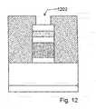
- the methodemploys a planarizing process to form a planarized dielectric surface 1102 as illustrated in FIG. 11 . This may be accomplished by a chemical mechanical polishing process, or a non isotropic chemical etch, for example, a blanket etch of the second dielectric material in a specific embodiment. As shown, a portion 1104 of the second dielectric material is maintained overlying a top region of the switching element in a specific embodiment.
- the methodincludes forming a first opening region 1202 in a portion of the second dielectric material to expose a portion of the top region of the switching element as shown in FIG. 12 . The first opening region is formed by using a second patterning and etching process in a specific embodiment.
- the first opening regionhas a first dimension in a specific embodiment.
- the etching processmay be a dry etch, such as a fluorine-based etching using CF 4 , SF 6 , or NF 3 , as the etching gas.
- a suitable wet etching techniquesuch as a HF-based etching may also be used depending on the embodiment.
- laser ablationmay be used to selectively remove the silicon oxide material overlying the switching material to form the first opening region.
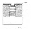
- the methodincludes forming a third dielectric material 1302 overlying the second dielectric layer including the first opening region as shown in FIG. 13 .
- the third dielectric materialis conformably formed overlying the second dielectric layer and the first opening region in a specific embodiment.
- the third dielectric materialcan be silicon nitride in a specific embodiment.
- Other suitable dielectric materialssuch as silicon oxide or a dielectric stack (for example, a silicon oxide on silicon nitride on silicon oxide stack, commonly known as ONO) may also be used depending on the embodiment.
- the methodsubjects the third dielectric material to a nonconformal or an anisotropic etching process to remove a portion of the third dielectric material to form a second opening region 1402 .
- the anisotropic etching processforms a side wall structure 1404 overlying the side region of the first opening region and a bottom region.
- the bottom regionincludes an exposed portion of the switching material in a specific embodiment. This etch is commonly used in semiconductor processing, and is known as a “sidewall spacer” etch.
- the exposed portionhas a second dimension, which is less than the first dimension.
- the methodforms a conductive material 1502 overlying at least the bottom region and the side wall structure.
- the conductive materialcan substantially fills the second opening region and in contact with the switching material in a specific embodiment.
- the conductive materialcan be conformably formed overlying the second opening region including the bottom region and the side wall structure depending on the deposition conditions.
- the conductive materialis in contact with the switching element, as shown.
- the conductive materialcan be a silver material.
- the silver materialcan be deposited using a physical deposition process such as sputtering or evaporation.
- the silver materialmay also be formed using a chemical deposition process such as chemical vapor deposition, electrochemical such as electroplating or electroless plating, or a combination depending on the application.
- the methodincludes forming a top barrier material 1602 overlying at least the conductive material and a top wiring material 1604 overlying the top barrier material as illustrated in FIG. 16 in a specific embodiment.
- the top barrier materialcan be a top adhesion material in a specific embodiment.
- the top barrier materialcan be titanium, titanium nitride, tantalum or tantalum nitride, tungsten, or tungsten nitride, or any suitable barrier material depending on the embodiment.
- top barrier layer 1602can be formed using a chemical deposition such as atomic layer deposition, chemical vapor deposition, and others, or a physical deposition such as sputtering, depending on the application.
- Top barrier material 1602can protect the conductive material, for example, the silver material from oxidation in a specific embodiment.
- Top barrier materialcan also be a diffusion barrier between the conductive material and the top wiring material in a specific embodiment.
- the top wiring materialcan be aluminum, tungsten, copper, or others.
- the top wiring structure materialmay be deposited using techniques such as physical vapor deposition process, for example, sputtering, evaporation, and others.
- the top wiring materialmay also be deposited using chemical deposition such as chemical vapor deposition, electrochemically including electroplating and electrodeless deposition depending on the embodiment.
- the methodsubjects a stack of material comprising the top wiring material, the top barrier material, and the contact material to a third pattern and etch process to from a top wiring structure.
- the conductive materialis in contact with the switching element.
- the top wiring structureis configured spatially at an angle to the bottom wiring structure to form a cross bar structure in a specific embodiment.
- the top wiring structureis configured spatially orthogonal to the bottom wiring structure.
- the switching elementis disposed in an intersection region of the top electrode structure and the bottom electrode structure.
- the stack of materialcan comprise of aluminum, titanium nitride, and silver, while silver is in contact with the amorphous silicon material.
- the above sequence of stepsprovides a method of forming a first array of memory cells for a vertically stacked device according to an embodiment of the present invention.
- the methodforms a fourth dielectric material 1702 overlying the top wiring structure of first array of memory cells.
- the fourth dielectric material 1702further fills in any gaps between the top interconnect wires.
- two memory cellsare illustrated in the first array of memory cells.
- the first array of memory cellscan have an X by Y array arranged in a crossbar configuration, where X and Y are integers and X>1, and Y>1.
- fourth dielectric material 1702can be silicon oxide, silicon nitride, or a dielectric stack with alternating dielectric materials, depending on the application.
- fourth dielectric material 1702forms a thickness 1704 overlying the first array of memory cells.
- the fourth dielectric materialis subjected to a planarizing process to form a planarized surface region.
- the methodforms a second array of memory cells overlying the planarized fourth dielectric material as shown in FIG. 18 .
- the second array of memory cellsincludes a plurality of memory cells.
- Each of the plurality of memory cellsincludes at least a second top electrode, a second bottom electrode, and a switching element sandwiched between the second top electrode and the second bottom electrode in a specific embodiment.
- the second top electrodeextends in a direction parallel to the first top electrode in a specific embodiment.
- the second bottom electrode and the second top electrodeare spatially arranged at an angle, and preferably orthogonal to each other in a crossbar configuration.
- the methodthan repeats the above steps of forming a memory array and dielectric material stack to form a vertically stacked memory device.
- each of the memory cells in an arraycan have an incipient diode to prevent program and read disturbs when selecting a device in an interconnecting array.
- the CMOS circuitry for programming the memory devicesis beneath the layers of memory cell arrays. Therefore, the CMOS devices do not occupy additional area on the substrate. Vertical stacking as illustrated in FIG. 8 allows for a high density device and a small die size.
- the methodcan form a plurality of via structures 1706 in a portion of the first dielectric material to connect the first array of memory cells with respective read, write, or erase circuitry provided by respective transistor devices on the semiconductor substrate.
- Via structure 1706may connect the first top wiring structure or the first bottom wiring layer.
- the via structureconnects to the first top wire layer.
- the via structurecan be formed using a pattern and etch process to form an interconnect structure.
- the methodincludes depositing an adhesion layer conformally formed overlying the via opening and an interconnect metal material overlying the adhesion layer to fill the plurality of via openings.
- the adhesion layercan be titanium, titanium nitride or tungsten nitride depending on the embodiment.
- the interconnect metal materialcan be tungsten, aluminum, copper or other suitable material.
- a metal planarizing processmay be performed to remove the metal interconnect material from the dielectric surface in a specific embodiment.
- the viamay be filled and metal deposited on top of the oxide 1704 . This metal may be patterned and etched to form the bottom wire layer for the next layer of memory array.
- the via structurecan be formed in an end region of each of the top wiring structure or the bottom wiring structure.
Landscapes
- Engineering & Computer Science (AREA)
- Manufacturing & Machinery (AREA)
- Semiconductor Memories (AREA)
Abstract
Description
Claims (20)
Priority Applications (4)
| Application Number | Priority Date | Filing Date | Title |
|---|---|---|---|
| US12/861,650US8492195B2 (en) | 2010-08-23 | 2010-08-23 | Method for forming stackable non-volatile resistive switching memory devices |
| US13/679,976US8648327B2 (en) | 2010-08-23 | 2012-11-16 | Stackable non-volatile resistive switching memory devices |
| US14/175,062US9035276B2 (en) | 2010-08-23 | 2014-02-07 | Stackable non-volatile resistive switching memory device |
| US14/715,159US9412789B1 (en) | 2010-08-23 | 2015-05-18 | Stackable non-volatile resistive switching memory device and method of fabricating the same |
Applications Claiming Priority (1)
| Application Number | Priority Date | Filing Date | Title |
|---|---|---|---|
| US12/861,650US8492195B2 (en) | 2010-08-23 | 2010-08-23 | Method for forming stackable non-volatile resistive switching memory devices |
Related Child Applications (1)
| Application Number | Title | Priority Date | Filing Date |
|---|---|---|---|
| US13/679,976DivisionUS8648327B2 (en) | 2010-08-23 | 2012-11-16 | Stackable non-volatile resistive switching memory devices |
Publications (2)
| Publication Number | Publication Date |
|---|---|
| US20120043621A1 US20120043621A1 (en) | 2012-02-23 |
| US8492195B2true US8492195B2 (en) | 2013-07-23 |
Family
ID=45593391
Family Applications (4)
| Application Number | Title | Priority Date | Filing Date |
|---|---|---|---|
| US12/861,650ActiveUS8492195B2 (en) | 2010-08-23 | 2010-08-23 | Method for forming stackable non-volatile resistive switching memory devices |
| US13/679,976ActiveUS8648327B2 (en) | 2010-08-23 | 2012-11-16 | Stackable non-volatile resistive switching memory devices |
| US14/175,062ActiveUS9035276B2 (en) | 2010-08-23 | 2014-02-07 | Stackable non-volatile resistive switching memory device |
| US14/715,159Expired - Fee RelatedUS9412789B1 (en) | 2010-08-23 | 2015-05-18 | Stackable non-volatile resistive switching memory device and method of fabricating the same |
Family Applications After (3)
| Application Number | Title | Priority Date | Filing Date |
|---|---|---|---|
| US13/679,976ActiveUS8648327B2 (en) | 2010-08-23 | 2012-11-16 | Stackable non-volatile resistive switching memory devices |
| US14/175,062ActiveUS9035276B2 (en) | 2010-08-23 | 2014-02-07 | Stackable non-volatile resistive switching memory device |
| US14/715,159Expired - Fee RelatedUS9412789B1 (en) | 2010-08-23 | 2015-05-18 | Stackable non-volatile resistive switching memory device and method of fabricating the same |
Country Status (1)
| Country | Link |
|---|---|
| US (4) | US8492195B2 (en) |
Cited By (1)
| Publication number | Priority date | Publication date | Assignee | Title |
|---|---|---|---|---|
| US20190164597A1 (en)* | 2017-11-29 | 2019-05-30 | International Business Machines Corporation | Synaptic crossbar memory array |
Families Citing this family (60)
| Publication number | Priority date | Publication date | Assignee | Title |
|---|---|---|---|---|
| US9601692B1 (en) | 2010-07-13 | 2017-03-21 | Crossbar, Inc. | Hetero-switching layer in a RRAM device and method |
| US9012307B2 (en) | 2010-07-13 | 2015-04-21 | Crossbar, Inc. | Two terminal resistive switching device structure and method of fabricating |
| US8946046B1 (en) | 2012-05-02 | 2015-02-03 | Crossbar, Inc. | Guided path for forming a conductive filament in RRAM |
| US9570678B1 (en) | 2010-06-08 | 2017-02-14 | Crossbar, Inc. | Resistive RAM with preferental filament formation region and methods |
| CN103081093B (en) | 2010-06-11 | 2015-06-03 | 科洛斯巴股份有限公司 | Pillar structure and method of memory device |
| US8374018B2 (en) | 2010-07-09 | 2013-02-12 | Crossbar, Inc. | Resistive memory using SiGe material |
| US8168506B2 (en) | 2010-07-13 | 2012-05-01 | Crossbar, Inc. | On/off ratio for non-volatile memory device and method |
| US8947908B2 (en) | 2010-11-04 | 2015-02-03 | Crossbar, Inc. | Hetero-switching layer in a RRAM device and method |
| US8569172B1 (en) | 2012-08-14 | 2013-10-29 | Crossbar, Inc. | Noble metal/non-noble metal electrode for RRAM applications |
| US8884261B2 (en) | 2010-08-23 | 2014-11-11 | Crossbar, Inc. | Device switching using layered device structure |
| US8841196B1 (en) | 2010-09-29 | 2014-09-23 | Crossbar, Inc. | Selective deposition of silver for non-volatile memory device fabrication |
| US8889521B1 (en) | 2012-09-14 | 2014-11-18 | Crossbar, Inc. | Method for silver deposition for a non-volatile memory device |
| US9401475B1 (en) | 2010-08-23 | 2016-07-26 | Crossbar, Inc. | Method for silver deposition for a non-volatile memory device |
| US8492195B2 (en) | 2010-08-23 | 2013-07-23 | Crossbar, Inc. | Method for forming stackable non-volatile resistive switching memory devices |
| US8558212B2 (en) | 2010-09-29 | 2013-10-15 | Crossbar, Inc. | Conductive path in switching material in a resistive random access memory device and control |
| US8391049B2 (en) | 2010-09-29 | 2013-03-05 | Crossbar, Inc. | Resistor structure for a non-volatile memory device and method |
| US8502185B2 (en) | 2011-05-31 | 2013-08-06 | Crossbar, Inc. | Switching device having a non-linear element |
| USRE46335E1 (en) | 2010-11-04 | 2017-03-07 | Crossbar, Inc. | Switching device having a non-linear element |
| US8258020B2 (en) | 2010-11-04 | 2012-09-04 | Crossbar Inc. | Interconnects for stacked non-volatile memory device and method |
| US8930174B2 (en) | 2010-12-28 | 2015-01-06 | Crossbar, Inc. | Modeling technique for resistive random access memory (RRAM) cells |
| US8791010B1 (en) | 2010-12-31 | 2014-07-29 | Crossbar, Inc. | Silver interconnects for stacked non-volatile memory device and method |
| US9153623B1 (en) | 2010-12-31 | 2015-10-06 | Crossbar, Inc. | Thin film transistor steering element for a non-volatile memory device |
| US8815696B1 (en) | 2010-12-31 | 2014-08-26 | Crossbar, Inc. | Disturb-resistant non-volatile memory device using via-fill and etchback technique |
| US9620206B2 (en) | 2011-05-31 | 2017-04-11 | Crossbar, Inc. | Memory array architecture with two-terminal memory cells |
| US8619459B1 (en) | 2011-06-23 | 2013-12-31 | Crossbar, Inc. | High operating speed resistive random access memory |
| US9564587B1 (en) | 2011-06-30 | 2017-02-07 | Crossbar, Inc. | Three-dimensional two-terminal memory with enhanced electric field and segmented interconnects |
| US8946669B1 (en) | 2012-04-05 | 2015-02-03 | Crossbar, Inc. | Resistive memory device and fabrication methods |
| US9166163B2 (en) | 2011-06-30 | 2015-10-20 | Crossbar, Inc. | Sub-oxide interface layer for two-terminal memory |
| US9627443B2 (en) | 2011-06-30 | 2017-04-18 | Crossbar, Inc. | Three-dimensional oblique two-terminal memory with enhanced electric field |
| US9252191B2 (en) | 2011-07-22 | 2016-02-02 | Crossbar, Inc. | Seed layer for a p+ silicon germanium material for a non-volatile memory device and method |
| US9729155B2 (en) | 2011-07-29 | 2017-08-08 | Crossbar, Inc. | Field programmable gate array utilizing two-terminal non-volatile memory |
| US10056907B1 (en) | 2011-07-29 | 2018-08-21 | Crossbar, Inc. | Field programmable gate array utilizing two-terminal non-volatile memory |
| US8674724B2 (en) | 2011-07-29 | 2014-03-18 | Crossbar, Inc. | Field programmable gate array utilizing two-terminal non-volatile memory |
| US9087576B1 (en) | 2012-03-29 | 2015-07-21 | Crossbar, Inc. | Low temperature fabrication method for a three-dimensional memory device and structure |
| US9685608B2 (en) | 2012-04-13 | 2017-06-20 | Crossbar, Inc. | Reduced diffusion in metal electrode for two-terminal memory |
| US8658476B1 (en) | 2012-04-20 | 2014-02-25 | Crossbar, Inc. | Low temperature P+ polycrystalline silicon material for non-volatile memory device |
| US8796658B1 (en) | 2012-05-07 | 2014-08-05 | Crossbar, Inc. | Filamentary based non-volatile resistive memory device and method |
| US8765566B2 (en) | 2012-05-10 | 2014-07-01 | Crossbar, Inc. | Line and space architecture for a non-volatile memory device |
| US9070859B1 (en) | 2012-05-25 | 2015-06-30 | Crossbar, Inc. | Low temperature deposition method for polycrystalline silicon material for a non-volatile memory device |
| US9583701B1 (en) | 2012-08-14 | 2017-02-28 | Crossbar, Inc. | Methods for fabricating resistive memory device switching material using ion implantation |
| US9741765B1 (en) | 2012-08-14 | 2017-08-22 | Crossbar, Inc. | Monolithically integrated resistive memory using integrated-circuit foundry compatible processes |
| US8946673B1 (en) | 2012-08-24 | 2015-02-03 | Crossbar, Inc. | Resistive switching device structure with improved data retention for non-volatile memory device and method |
| US9680094B2 (en)* | 2012-08-30 | 2017-06-13 | Kabushiki Kaisha Toshiba | Memory device and method for manufacturing the same |
| US9312483B2 (en) | 2012-09-24 | 2016-04-12 | Crossbar, Inc. | Electrode structure for a non-volatile memory device and method |
| US9576616B2 (en) | 2012-10-10 | 2017-02-21 | Crossbar, Inc. | Non-volatile memory with overwrite capability and low write amplification |
| US11068620B2 (en) | 2012-11-09 | 2021-07-20 | Crossbar, Inc. | Secure circuit integrated with memory layer |
| US8982647B2 (en) | 2012-11-14 | 2015-03-17 | Crossbar, Inc. | Resistive random access memory equalization and sensing |
| US9412790B1 (en) | 2012-12-04 | 2016-08-09 | Crossbar, Inc. | Scalable RRAM device architecture for a non-volatile memory device and method |
| US9406379B2 (en) | 2013-01-03 | 2016-08-02 | Crossbar, Inc. | Resistive random access memory with non-linear current-voltage relationship |
| US9324942B1 (en) | 2013-01-31 | 2016-04-26 | Crossbar, Inc. | Resistive memory cell with solid state diode |
| US9112145B1 (en) | 2013-01-31 | 2015-08-18 | Crossbar, Inc. | Rectified switching of two-terminal memory via real time filament formation |
| US8934280B1 (en) | 2013-02-06 | 2015-01-13 | Crossbar, Inc. | Capacitive discharge programming for two-terminal memory cells |
| KR102114202B1 (en) | 2013-11-25 | 2020-05-26 | 삼성전자주식회사 | Non volatile memory device and method of forming the same |
| US10290801B2 (en) | 2014-02-07 | 2019-05-14 | Crossbar, Inc. | Scalable silicon based resistive memory device |
| US10832127B2 (en) | 2015-11-30 | 2020-11-10 | Samsung Electronics Co., Ltd. | Three-dimensional integration of neurosynaptic chips |
| FR3066038B1 (en)* | 2017-05-05 | 2020-01-24 | Stmicroelectronics (Crolles 2) Sas | PHASE CHANGE MEMORY |
| CN111293138A (en)* | 2018-12-07 | 2020-06-16 | 中国科学院上海微系统与信息技术研究所 | Three-dimensional MRAM storage structure and fabrication method thereof |
| KR102832683B1 (en) | 2020-07-09 | 2025-07-14 | 삼성전자주식회사 | Variable resistance memory device |
| US11258023B1 (en)* | 2020-08-05 | 2022-02-22 | Nantero, Inc. | Resistive change elements using passivating interface gaps and methods for making same |
| US20240389486A1 (en)* | 2023-05-15 | 2024-11-21 | Taiwan Semiconductor Manufacturing Company Limited | Capacitor circuit providing self-adjusting capacitance and methods for forming the same |
Citations (134)
| Publication number | Priority date | Publication date | Assignee | Title |
|---|---|---|---|---|
| US680652A (en) | 1897-11-08 | 1901-08-13 | Leonard L Elden | Circuit-breaker. |
| US4433468A (en) | 1980-03-26 | 1984-02-28 | Nippon Electric Co., Ltd. | Method for making semiconductor device having improved thermal stress characteristics |
| US4684972A (en) | 1981-08-07 | 1987-08-04 | The British Petroleum Company, P.L.C. | Non-volatile amorphous semiconductor memory device utilizing a forming voltage |
| US4741601A (en) | 1984-10-08 | 1988-05-03 | Nec Corporation | Non-linear device for driving liquid crystal display |
| US5242855A (en) | 1991-09-30 | 1993-09-07 | Nec Corporation | Method of fabricating a polycrystalline silicon film having a reduced resistivity |
| US5278085A (en) | 1992-08-11 | 1994-01-11 | Micron Semiconductor, Inc. | Single mask process for forming both n-type and p-type gates in a polycrystalline silicon layer during the formation of a semiconductor device |
| US5315131A (en) | 1990-11-22 | 1994-05-24 | Matsushita Electric Industrial Co., Ltd. | Electrically reprogrammable nonvolatile memory device |
| US5335219A (en) | 1991-01-18 | 1994-08-02 | Ovshinsky Stanford R | Homogeneous composition of microcrystalline semiconductor material, semiconductor devices and directly overwritable memory elements fabricated therefrom, and arrays fabricated from the memory elements |
| US5360981A (en) | 1989-05-11 | 1994-11-01 | British Telecommunications Public Limited Company | Amorphous silicon memory |
| US5457649A (en) | 1994-08-26 | 1995-10-10 | Microchip Technology, Inc. | Semiconductor memory device and write-once, read-only semiconductor memory array using amorphous-silicon and method therefor |
| US5538564A (en) | 1994-03-18 | 1996-07-23 | Regents Of The University Of California | Three dimensional amorphous silicon/microcrystalline silicon solar cells |
| US5541869A (en) | 1991-10-22 | 1996-07-30 | British Telecommunications, Plc | Resistive memory element |
| US5594363A (en) | 1995-04-07 | 1997-01-14 | Zycad Corporation | Logic cell and routing architecture in a field programmable gate array |
| US5614756A (en) | 1990-04-12 | 1997-03-25 | Actel Corporation | Metal-to-metal antifuse with conductive |
| US5751012A (en) | 1995-06-07 | 1998-05-12 | Micron Technology, Inc. | Polysilicon pillar diode for use in a non-volatile memory cell |
| US5840608A (en) | 1996-11-22 | 1998-11-24 | United Microelectronics Corporation | High density ROM and a method of making the same |
| US5970332A (en) | 1995-03-28 | 1999-10-19 | U.S. Philips Corporation | Method of manufacturing a semiconductor device with a BiCMOS circuit |
| US5998244A (en) | 1996-08-22 | 1999-12-07 | Micron Technology, Inc. | Memory cell incorporating a chalcogenide element and method of making same |
| US6128214A (en) | 1999-03-29 | 2000-10-03 | Hewlett-Packard | Molecular wire crossbar memory |
| US6143642A (en) | 1997-12-22 | 2000-11-07 | Vlsi Technology, Inc. | Programmable semiconductor structures and methods for making the same |
| US6259116B1 (en) | 1997-10-22 | 2001-07-10 | U.S. Philips Corporation | Multiple memory element semiconductor memory devices |
| US6291836B1 (en) | 1996-06-05 | 2001-09-18 | U. S. Philips Corporation | Method of operating a programmable, non-volatile memory device |
| US6436765B1 (en) | 2001-02-09 | 2002-08-20 | United Microelectronics Corp. | Method of fabricating a trenched flash memory cell |
| US6436818B1 (en) | 1997-02-19 | 2002-08-20 | Micron Technology, Inc. | Semiconductor structure having a doped conductive layer |
| US6492694B2 (en) | 1998-02-27 | 2002-12-10 | Micron Technology, Inc. | Highly conductive composite polysilicon gate for CMOS integrated circuits |
| US20040026682A1 (en) | 2002-06-17 | 2004-02-12 | Hai Jiang | Nano-dot memory and fabricating same |
| US6768157B2 (en) | 2001-08-13 | 2004-07-27 | Advanced Micro Devices, Inc. | Memory device |
| US6815286B2 (en) | 2001-08-13 | 2004-11-09 | Advanced Micro Devices, Inc. | Memory device |
| US6838720B2 (en) | 2001-08-13 | 2005-01-04 | Advanced Micro Devices, Inc. | Memory device with active passive layers |
| US20050020510A1 (en) | 2002-08-29 | 2005-01-27 | Benedict Dale L. | D-mannose contraceptives |
| US20050029587A1 (en) | 1995-06-07 | 2005-02-10 | Harshfield Steven T. | Method and apparatus for forming an integrated circuit electrode having a reduced contact area |
| US6858482B2 (en) | 2002-04-10 | 2005-02-22 | Micron Technology, Inc. | Method of manufacture of programmable switching circuits and memory cells employing a glass layer |
| US6858481B2 (en) | 2001-08-13 | 2005-02-22 | Advanced Micro Devices, Inc. | Memory device with active and passive layers |
| US6864127B2 (en) | 1997-04-25 | 2005-03-08 | Semiconductor Energy Laboratory Co., Ltd. | Semiconductor device and method of fabricating the same |
| US6927430B2 (en) | 2001-06-28 | 2005-08-09 | Sharp Laboratories Of America, Inc. | Shared bit line cross-point memory array incorporating P/N junctions |
| US6939787B2 (en) | 1999-12-28 | 2005-09-06 | Fujitsu Limited | Method for fabricating semiconductor device having gate electrode with polymetal structure of polycrystalline silicon film and metal film |
| US6946719B2 (en) | 2003-12-03 | 2005-09-20 | Matrix Semiconductor, Inc | Semiconductor device including junction diode contacting contact-antifuse unit comprising silicide |
| US7020006B2 (en) | 2002-08-02 | 2006-03-28 | Unity Semiconductor Corporation | Discharge of conductive array lines in fast memory |
| US7023093B2 (en) | 2002-10-24 | 2006-04-04 | International Business Machines Corporation | Very low effective dielectric constant interconnect Structures and methods for fabricating the same |
| US7102150B2 (en) | 2001-05-11 | 2006-09-05 | Harshfield Steven T | PCRAM memory cell and method of making same |
| US7122853B1 (en) | 2004-08-17 | 2006-10-17 | Fasl, Inc. | Method to improve yield and simplify operation of polymer memory cells |
| US20070008773A1 (en) | 2005-07-11 | 2007-01-11 | Matrix Semiconductor, Inc. | Nonvolatile memory cell comprising switchable resistor and transistor |
| US20070015348A1 (en) | 2005-07-18 | 2007-01-18 | Sharp Laboratories Of America, Inc. | Crosspoint resistor memory device with back-to-back Schottky diodes |
| US7187577B1 (en) | 2005-11-23 | 2007-03-06 | Grandis, Inc. | Method and system for providing current balanced writing for memory cells and magnetic devices |
| US20070087508A1 (en) | 2003-12-03 | 2007-04-19 | Herner S B | Method for making a p-i-n diode crystallized adjacent to a silicide in series with a dielectric antifuse |
| US20070105390A1 (en) | 2005-11-09 | 2007-05-10 | Oh Travis B | Oxygen depleted etching process |
| US20070105284A1 (en) | 2003-12-03 | 2007-05-10 | Herner S B | Method for forming a memory cell comprising a semiconductor junction diode crystallized adjacent to a silicide |
| US7221599B1 (en) | 2004-11-01 | 2007-05-22 | Spansion, Llc | Polymer memory cell operation |
| US7238607B2 (en) | 2002-12-19 | 2007-07-03 | Sandisk 3D Llc | Method to minimize formation of recess at surface planarized by chemical mechanical planarization |
| US20070205510A1 (en) | 2006-03-03 | 2007-09-06 | Lavoie Adrien R | Noble metal barrier layers |
| US7289353B2 (en) | 2004-08-17 | 2007-10-30 | Spansion, Llc | Systems and methods for adjusting programming thresholds of polymer memory cells |
| US20070290186A1 (en) | 2006-05-04 | 2007-12-20 | El Mostafa Bourim | Non-volatile variable resistance memory device and method of fabricating the same |
| US20080002481A1 (en) | 2002-12-20 | 2008-01-03 | Dietmar Gogl | Integrated Circuit, Method of Operating an Integrated Circuit, Method of Manufacturing an Integrated Circuit, Memory Module, Stackable Memory Module |
| US20080006907A1 (en) | 2006-07-06 | 2008-01-10 | Samsung Electronics Co., Ltd | Non-volatile memory device including a variable resistance material |
| US20080048164A1 (en) | 2006-07-11 | 2008-02-28 | Matsushita Electric Industrial Co., Ltd. | Electro-resistance element, method of manufacturing the same and electro-resistance memory using the same |
| US20080090337A1 (en) | 2006-10-03 | 2008-04-17 | Williams R Stanley | Electrically actuated switch |
| US20080089110A1 (en) | 2006-10-16 | 2008-04-17 | Warren Robinett | Crossbar-memory systems and methods for writing to and reading from crossbar memory junctions of crossbar-memory systems |
| US7365411B2 (en) | 2004-08-12 | 2008-04-29 | Micron Technology, Inc. | Resistance variable memory with temperature tolerant materials |
| US20080106926A1 (en) | 2006-11-08 | 2008-05-08 | Symetrix Corporation | Non-volatile resistance switching memories and methods of making same |
| US20080106925A1 (en) | 2006-11-08 | 2008-05-08 | Symetrix Corporation | Correlated electron memory |
| US7405418B2 (en)* | 2004-02-17 | 2008-07-29 | Infineon Technologies Ag | Memory device electrode with a surface structure |
| US20080206931A1 (en) | 2002-07-26 | 2008-08-28 | Laurent Breuil | Nonvolatile memory element and production method thereof and storage memory arrangement |
| US7474000B2 (en) | 2003-12-05 | 2009-01-06 | Sandisk 3D Llc | High density contact to relaxed geometry layers |
| US20090014707A1 (en) | 2006-10-20 | 2009-01-15 | Wei Lu | Non-volatile solid state resistive switching devices |
| US20090052226A1 (en) | 2007-08-24 | 2009-02-26 | Samsung Electronics Co., Ltd | Resistive random access memory device |
| US7521705B2 (en) | 2005-08-15 | 2009-04-21 | Micron Technology, Inc. | Reproducible resistance variable insulating memory devices having a shaped bottom electrode |
| US7534625B2 (en) | 2004-09-24 | 2009-05-19 | Karpov Ilya V | Phase change memory with damascene memory element |
| US7550380B2 (en) | 2004-11-03 | 2009-06-23 | Micron Technology, Inc. | Electroless plating of metal caps for chalcogenide-based memory devices |
| US20090231910A1 (en) | 2008-03-11 | 2009-09-17 | Micron Technology, Inc. | Non-volatile memory with resistive access component |
| US20090250787A1 (en) | 2008-04-07 | 2009-10-08 | Toshie Kutsunai | Semiconductor storage device and manufacturing method of the same |
| US20090256130A1 (en) | 2008-04-11 | 2009-10-15 | Sandisk 3D Llc | Memory cell that employs a selectively fabricated carbon nano-tube reversible resistance-switching element, and methods of forming the same |
| US7606059B2 (en) | 2003-03-18 | 2009-10-20 | Kabushiki Kaisha Toshiba | Three-dimensional programmable resistance memory device with a read/write circuit stacked under a memory cell array |
| US7615439B1 (en) | 2008-09-29 | 2009-11-10 | Sandisk Corporation | Damascene process for carbon memory element with MIIM diode |
| US20090298224A1 (en)* | 2002-12-13 | 2009-12-03 | Lowrey Tyler A | Memory and Access Device and Method Therefor |
| US20090321789A1 (en) | 2008-06-30 | 2009-12-31 | Sandisk 3D Llc | Triangle two dimensional complementary patterning of pillars |
| US20100012914A1 (en) | 2008-07-18 | 2010-01-21 | Sandisk 3D Llc | Carbon-based resistivity-switching materials and methods of forming the same |
| US20100019310A1 (en) | 2008-07-25 | 2010-01-28 | Kabushiki Kaisha Toshiba | Semiconductor memory device |
| US20100032638A1 (en) | 2008-08-07 | 2010-02-11 | Sandisk 3D Llc | Memory cell that includes a carbon-based memory element and methods of forming the same |
| US20100084625A1 (en) | 2008-10-02 | 2010-04-08 | Guy Wicker | Memory Device |
| US20100085798A1 (en) | 2008-10-08 | 2010-04-08 | The Regents Of The University Of Michigan | Silicon-based nanoscale resistive device with adjustable resistance |
| US20100090192A1 (en) | 2006-08-31 | 2010-04-15 | Nxp, B.V. | Method for controlled formation of the resistive switching material in a resistive switching device and device obtained thereof |
| US20100101290A1 (en) | 2008-10-24 | 2010-04-29 | Antonio Bertolotto | Method for the production of an agent for treatment of agricultural soils |
| US20100102290A1 (en) | 2008-10-20 | 2010-04-29 | The Regents Of The University Of Michigan | Silicon based nanoscale crossbar memory |
| US7728318B2 (en) | 2006-11-16 | 2010-06-01 | Sandisk Corporation | Nonvolatile phase change memory cell having a reduced contact area |
| US7729158B2 (en)* | 2003-04-03 | 2010-06-01 | Kabushiki Kaisha Toshiba | Resistance change memory device |
| US20100157710A1 (en) | 2008-12-19 | 2010-06-24 | Unity Semiconductor Corporation | Array Operation Using A Schottky Diode As a Non-Ohmic Isolation Device |
| US20100176368A1 (en)* | 2009-01-14 | 2010-07-15 | Ko Nikka | Method of manufacturing semiconductor memory device, and semiconductor memory device |
| US7772581B2 (en) | 2006-09-11 | 2010-08-10 | Macronix International Co., Ltd. | Memory device having wide area phase change element and small electrode contact area |
| US7786464B2 (en) | 2007-11-20 | 2010-08-31 | Infineon Technologies Ag | Integrated circuit having dielectric layer including nanocrystals |
| US7786589B2 (en) | 2006-12-06 | 2010-08-31 | Kabushiki Kaisha Toshiba | Semiconductor device and method for manufacturing semiconductor device |
| US20100219510A1 (en) | 2008-06-30 | 2010-09-02 | Sandisk 3D Llc | Method for fabricating high density pillar structures by double patterning using positive photoresist |
| US7824956B2 (en) | 2007-06-29 | 2010-11-02 | Sandisk 3D Llc | Memory cell that employs a selectively grown reversible resistance-switching element and methods of forming the same |
| US7829875B2 (en) | 2006-03-31 | 2010-11-09 | Sandisk 3D Llc | Nonvolatile rewritable memory cell comprising a resistivity-switching oxide or nitride and an antifuse |
| US7835170B2 (en) | 2005-05-09 | 2010-11-16 | Nantero, Inc. | Memory elements and cross point switches and arrays of same using nonvolatile nanotube blocks |
| US20100321095A1 (en)* | 2008-06-10 | 2010-12-23 | Takumi Mikawa | Semiconductor device, manufacturing method of semiconductor device, semiconductor chip and system |
| US7859884B2 (en) | 2005-01-19 | 2010-12-28 | Sandisk 3D Llc | Structure and method for biasing phase change memory array for reliable writing |
| US7875871B2 (en) | 2006-03-31 | 2011-01-25 | Sandisk 3D Llc | Heterojunction device comprising a semiconductor and a resistivity-switching oxide or nitride |
| US7881097B2 (en) | 2006-12-26 | 2011-02-01 | Sony Corporation | Storage element and memory |
| US7898838B2 (en) | 2008-10-31 | 2011-03-01 | Seagate Technology Llc | Resistive sense memory calibration for self-reference read method |
| US7897953B2 (en) | 2008-01-16 | 2011-03-01 | Micron Technology, Inc. | Multi-level programmable PCRAM memory |
| US7920412B2 (en) | 2006-09-29 | 2011-04-05 | Kabushiki Kaisha Toshiba | Magnetic random access memory and method of manufacturing the same |
| US7924138B2 (en) | 2007-03-01 | 2011-04-12 | Fujitsu Limited | Semiconductor device and manufacturing method of the same |
| US20110133149A1 (en) | 2009-12-04 | 2011-06-09 | Sonehara Takeshi | Resistance change memory and manufacturing method thereof |
| US7968419B2 (en) | 2005-07-18 | 2011-06-28 | Sharp Laboratories Of America, Inc. | Back-to-back metal/semiconductor/metal (MSM) Schottky diode |
| US20110155991A1 (en) | 2009-12-29 | 2011-06-30 | Industrial Technology Research Institute | Resistive memory device and fabricating method thereof |
| US20110198557A1 (en) | 2008-02-07 | 2011-08-18 | International Business Machines Corporation | Method for fabrication of crystalline diodes for resistive memories |
| US8004882B2 (en) | 2004-06-04 | 2011-08-23 | Micron Technology, Inc. | Spintronic devices with integrated transistors |
| US20110212616A1 (en) | 2010-02-26 | 2011-09-01 | Robert Seidel | Metallization system of a semiconductor device comprising rounded interconnects formed by hard mask rounding |
| US8018760B2 (en) | 2006-12-28 | 2011-09-13 | Panasonic Corporation | Resistance variable element and resistance variable memory apparatus |
| US20110227028A1 (en) | 2010-03-16 | 2011-09-22 | Deepak Chandra Sekar | Bottom electrodes for use with metal oxide resistivity switching layers |
| US8045364B2 (en) | 2009-12-18 | 2011-10-25 | Unity Semiconductor Corporation | Non-volatile memory device ion barrier |
| US8054674B2 (en) | 2007-05-10 | 2011-11-08 | Sharp Kabushiki Kaisha | Variable resistive element, manufacturing method for same, and non-volatile semiconductor memory device |
| US20110284814A1 (en) | 2010-05-24 | 2011-11-24 | Guobiao Zhang | Large Bit-Per-Cell Three-Dimensional Mask-Programmable Read-Only Memory |
| US8067815B2 (en) | 2008-12-11 | 2011-11-29 | Macronix International Co., Lt.d. | Aluminum copper oxide based memory devices and methods for manufacture |
| US20110317470A1 (en)* | 2010-06-24 | 2011-12-29 | The Regents Of The University Of Michigan | Rectification element and method for resistive switching for non volatile memory device |
| US8088688B1 (en) | 2010-11-05 | 2012-01-03 | Crossbar, Inc. | p+ polysilicon material on aluminum for non-volatile memory device and method |
| US20120008366A1 (en) | 2010-07-09 | 2012-01-12 | Crossbar, Inc. | RESTIVE MEMORY USING SiGe MATERIAL |
| US8097874B2 (en) | 2008-10-30 | 2012-01-17 | Seagate Technology Llc | Programmable resistive memory cell with sacrificial metal |
| US20120015506A1 (en) | 2010-07-13 | 2012-01-19 | Crossbar, Inc. | Two terminal resistive switching device structure and method of fabricating |
| US20120012806A1 (en) | 2010-07-13 | 2012-01-19 | Crossbar, Inc. | Improved on/off ratio for non-volatile memory device and method |
| US20120025161A1 (en) | 2008-02-27 | 2012-02-02 | Manuj Rathor | Diode and resistive memory device structures |
| US20120033479A1 (en) | 2010-08-06 | 2012-02-09 | Lsi Corporation | Modification of logic by morphological manipulation of a semiconductor resistive element |
| US20120043654A1 (en) | 2010-08-19 | 2012-02-23 | Taiwan Semiconductor Manufacturing Company, Ltd. | Mechanisms for forming copper pillar bumps using patterned anodes |
| US20120043519A1 (en) | 2010-08-23 | 2012-02-23 | Crossbar, Inc. | Device switching using layered device structure |
| US8144498B2 (en) | 2007-05-09 | 2012-03-27 | Intermolecular, Inc. | Resistive-switching nonvolatile memory elements |
| US8143092B2 (en) | 2008-03-10 | 2012-03-27 | Pragati Kumar | Methods for forming resistive switching memory elements by heating deposited layers |
| US20120104351A1 (en) | 2010-07-01 | 2012-05-03 | Zhiqiang Wei | Non-volatile memory cell, non-volatile memory cell array, and method of manufacturing the same |
| US8183553B2 (en) | 2009-04-10 | 2012-05-22 | Intermolecular, Inc. | Resistive switching memory element including doped silicon electrode |
| US20120145984A1 (en) | 2010-12-13 | 2012-06-14 | Peter Rabkin | Punch-through diode |
| US20120155146A1 (en) | 2010-12-20 | 2012-06-21 | Yoshihiro Ueda | Resistance-change memory |
| US8207064B2 (en) | 2009-09-17 | 2012-06-26 | Sandisk 3D Llc | 3D polysilicon diode with low contact resistance and method for forming same |
| US8233308B2 (en) | 2007-06-29 | 2012-07-31 | Sandisk 3D Llc | Memory cell that employs a selectively deposited reversible resistance-switching element and methods of forming the same |
| US20120235112A1 (en) | 2010-11-30 | 2012-09-20 | Huo Zongliang | Resistive switching memory and method for manufacturing the same |
| US8394670B2 (en) | 2011-05-31 | 2013-03-12 | Crossbar, Inc. | Vertical diodes for non-volatile memory device |
Family Cites Families (130)
| Publication number | Priority date | Publication date | Assignee | Title |
|---|---|---|---|---|
| JPH02181160A (en) | 1989-01-04 | 1990-07-13 | Fuji Xerox Co Ltd | Electrophotographic sensitive body |
| JPH0590224A (en) | 1991-01-22 | 1993-04-09 | Toshiba Corp | Method for manufacturing semiconductor device |
| KR960005765A (en) | 1994-07-14 | 1996-02-23 | 모리시다 요이치 | Electroless plating bath and wiring forming method of semiconductor device used for wiring formation of semiconductor device |
| DE69510337T2 (en) | 1994-12-22 | 1999-12-16 | Koninklijke Philips Electronics N.V., Eindhoven | SEMICONDUCTOR MEMORY ARRANGEMENTS AND PRODUCTION METHOD |
| JP4034380B2 (en) | 1996-10-31 | 2008-01-16 | 株式会社東芝 | Image encoding / decoding method and apparatus |
| US6180998B1 (en) | 1998-03-30 | 2001-01-30 | Lsi Logic Corporation | DRAM with built-in noise protection |
| JP2000012787A (en) | 1998-06-10 | 2000-01-14 | Lucent Technol Inc | Integrated circuit device and method for forming resistance elements used in integrated circuit |
| US6603883B1 (en) | 1998-09-08 | 2003-08-05 | Canon Kabushiki Kaisha | Image processing apparatus including an image data encoder having at least two scalability modes and method therefor |
| JP2000124195A (en) | 1998-10-14 | 2000-04-28 | Tokyo Electron Ltd | Surface treatment method and device |
| US7157314B2 (en) | 1998-11-16 | 2007-01-02 | Sandisk Corporation | Vertically stacked field programmable nonvolatile memory and method of fabrication |
| US6288435B1 (en) | 1999-12-28 | 2001-09-11 | Xerox Corporation | Continuous amorphous silicon layer sensors using doped poly-silicon back contact |
| US6563156B2 (en) | 2001-03-15 | 2003-05-13 | Micron Technology, Inc. | Memory elements and methods for making same |
| KR100821456B1 (en) | 2000-08-14 | 2008-04-11 | 샌디스크 쓰리디 엘엘씨 | Dense array and charge storage device and manufacturing method thereof |
| US6627530B2 (en) | 2000-12-22 | 2003-09-30 | Matrix Semiconductor, Inc. | Patterning three dimensional structures |
| US6806526B2 (en) | 2001-08-13 | 2004-10-19 | Advanced Micro Devices, Inc. | Memory device |
| US7109056B2 (en) | 2001-09-20 | 2006-09-19 | Micron Technology, Inc. | Electro-and electroless plating of metal in the manufacture of PCRAM devices |
| WO2003034498A1 (en) | 2001-10-16 | 2003-04-24 | Midwest Research Institute | Stacked switchable element and diode combination |
| US20030141565A1 (en) | 2002-01-28 | 2003-07-31 | Fumihiko Hirose | Diode |
| JP3948292B2 (en) | 2002-02-01 | 2007-07-25 | 株式会社日立製作所 | Semiconductor memory device and manufacturing method thereof |
| US7087919B2 (en) | 2002-02-20 | 2006-08-08 | Micron Technology, Inc. | Layered resistance variable memory device and method of fabrication |
| US6643213B2 (en) | 2002-03-12 | 2003-11-04 | Hewlett-Packard Development Company, L.P. | Write pulse circuit for a magnetic memory |
| US6870755B2 (en) | 2002-08-02 | 2005-03-22 | Unity Semiconductor Corporation | Re-writable memory with non-linear memory element |
| US6867996B2 (en) | 2002-08-29 | 2005-03-15 | Micron Technology, Inc. | Single-polarity programmable resistance-variable memory element |
| US6848012B2 (en) | 2002-09-27 | 2005-01-25 | Broadcom Corporation | Method and system for an adaptive multimode media queue |
| US6873015B2 (en) | 2002-10-02 | 2005-03-29 | Micron Technology, Inc. | Semiconductor constructions comprising three-dimensional thin film transistor devices and resistors |
| US6821879B2 (en) | 2002-10-30 | 2004-11-23 | Xerox Corporation | Copper interconnect by immersion/electroless plating in dual damascene process |
| US8637366B2 (en) | 2002-12-19 | 2014-01-28 | Sandisk 3D Llc | Nonvolatile memory cell without a dielectric antifuse having high- and low-impedance states |
| US7800932B2 (en) | 2005-09-28 | 2010-09-21 | Sandisk 3D Llc | Memory cell comprising switchable semiconductor memory element with trimmable resistance |
| JP2004319587A (en) | 2003-04-11 | 2004-11-11 | Sharp Corp | Memory cell, memory device, and memory cell manufacturing method |
| EP1489622B1 (en) | 2003-06-16 | 2007-08-15 | STMicroelectronics S.r.l. | Writing circuit for a phase change memory device |
| JP2005109236A (en) | 2003-09-30 | 2005-04-21 | Toshiba Corp | Nonvolatile semiconductor memory device and manufacturing method thereof |
| US7136300B2 (en) | 2003-10-06 | 2006-11-14 | Hewlett-Packard Development Company, Lp. | Magnetic memory device including groups of series-connected memory elements |
| EP2270795A3 (en) | 2003-11-10 | 2015-03-18 | Panasonic Corporation | Recording medium, playback apparatus, program, playback method, system integrated circuit |
| US7139198B2 (en) | 2004-01-27 | 2006-11-21 | Sandisk Corporation | Efficient verification for coarse/fine programming of non-volatile memory |
| US20050175099A1 (en) | 2004-02-06 | 2005-08-11 | Nokia Corporation | Transcoder and associated system, method and computer program product for low-complexity reduced resolution transcoding |
| JP2005277066A (en)* | 2004-03-24 | 2005-10-06 | Seiko Epson Corp | Ferroelectric memory device and manufacturing method thereof |
| US7084691B2 (en) | 2004-07-21 | 2006-08-01 | Sharp Laboratories Of America, Inc. | Mono-polarity switchable PCMO resistor trimmer |
| US7405465B2 (en) | 2004-09-29 | 2008-07-29 | Sandisk 3D Llc | Deposited semiconductor structure to minimize n-type dopant diffusion and method of making |
| US7749805B2 (en) | 2005-03-10 | 2010-07-06 | Qimonda Ag | Method for manufacturing an integrated circuit including an electrolyte material layer |
| US7323349B2 (en) | 2005-05-02 | 2008-01-29 | Sharp Laboratories Of America, Inc. | Self-aligned cross point resistor memory array |
| JP2006344746A (en) | 2005-06-08 | 2006-12-21 | Toshiba Corp | Nonvolatile semiconductor memory device and manufacturing method thereof |
| US7303971B2 (en) | 2005-07-18 | 2007-12-04 | Sharp Laboratories Of America, Inc. | MSM binary switch memory device |
| KR100630437B1 (en) | 2005-08-31 | 2006-10-02 | 삼성전자주식회사 | Nonvolatile Organic Resistance Memory Device and Manufacturing Method Thereof |
| US7324363B2 (en) | 2005-12-12 | 2008-01-29 | Synopsys, Inc. | SPICE optimized for arrays |
| WO2007116749A1 (en)* | 2006-03-30 | 2007-10-18 | Matsushita Electric Industrial Co., Ltd. | Nonvolatile memory element and its manufacturing method |
| JP2007281208A (en) | 2006-04-07 | 2007-10-25 | Matsushita Electric Ind Co Ltd | Multilayer variable resistance element array, variable resistance device, multilayer nonvolatile memory element array, and nonvolatile memory device |
| JP4297136B2 (en) | 2006-06-07 | 2009-07-15 | ソニー株式会社 | Storage device |
| US7626518B2 (en) | 2006-06-08 | 2009-12-01 | Via Technologies, Inc. | Decoding systems and methods in computational core of programmable graphics processing unit |
| KR101159075B1 (en) | 2006-06-27 | 2012-06-25 | 삼성전자주식회사 | Variable resistance random access memory device comprising n+ interfacial layer |
| US7719001B2 (en) | 2006-06-28 | 2010-05-18 | Semiconductor Energy Laboratory Co., Ltd | Semiconductor device with metal oxides and an organic compound |
| US7499355B2 (en) | 2006-07-31 | 2009-03-03 | Sandisk 3D Llc | High bandwidth one time field-programmable memory |
| JP4869006B2 (en) | 2006-09-27 | 2012-02-01 | 株式会社東芝 | Method for controlling semiconductor memory device |
| KR100782496B1 (en) | 2006-11-09 | 2007-12-05 | 삼성전자주식회사 | Method for manufacturing semiconductor device having self-aligned cell diode and method for manufacturing phase change memory device using same |
| JP5232159B2 (en) | 2006-11-09 | 2013-07-10 | セイジ・エレクトロクロミクス,インコーポレイテッド | Method of making an ion-switching device without an independent lithiation step |
| JP4088324B1 (en) | 2006-12-08 | 2008-05-21 | シャープ株式会社 | Nonvolatile semiconductor memory device |
| EP1933563A1 (en) | 2006-12-14 | 2008-06-18 | Thomson Licensing | Method and apparatus for encoding and/or decoding bit depth scalable video data using adaptive enhancement layer residual prediction |
| US7972897B2 (en) | 2007-02-05 | 2011-07-05 | Intermolecular, Inc. | Methods for forming resistive switching memory elements |
| US8265136B2 (en) | 2007-02-20 | 2012-09-11 | Vixs Systems, Inc. | Motion refinement engine for use in video encoding in accordance with a plurality of sub-pixel resolutions and methods for use therewith |
| KR100852233B1 (en) | 2007-02-21 | 2008-08-13 | 삼성전자주식회사 | Formation method of vertical diode and manufacturing method of phase change memory device using same |
| US7382647B1 (en) | 2007-02-27 | 2008-06-03 | International Business Machines Corporation | Rectifying element for a crosspoint based memory array architecture |
| US20080205179A1 (en) | 2007-02-28 | 2008-08-28 | Qimonda Ag | Integrated circuit having a memory array |
| US7629198B2 (en) | 2007-03-05 | 2009-12-08 | Intermolecular, Inc. | Methods for forming nonvolatile memory elements with resistive-switching metal oxides |
| US8231998B2 (en) | 2007-03-30 | 2012-07-31 | The Regents Of The University Of Michigan | Deposited microarchitectured battery and manufacturing method |
| US7984776B2 (en) | 2007-03-30 | 2011-07-26 | The Regents Of The University Of Michigan | Energy storage and control system for a vehicle electrified drivetrain |
| US7800094B2 (en) | 2007-06-11 | 2010-09-21 | Macronix International Co., Ltd. | Resistance memory with tungsten compound and manufacturing |
| US7855119B2 (en) | 2007-06-15 | 2010-12-21 | Sandisk 3D Llc | Method for forming polycrystalline thin film bipolar transistors |
| US8145002B2 (en) | 2007-06-28 | 2012-03-27 | Mitsubishi Electric Corporation | Image encoding device and image encoding method |
| TW200915543A (en) | 2007-06-29 | 2009-04-01 | Sandisk 3D Llc | Memory cell that employs a selectively grown reversible resistance-switching element and methods of forming the same |
| US7846785B2 (en) | 2007-06-29 | 2010-12-07 | Sandisk 3D Llc | Memory cell that employs a selectively deposited reversible resistance-switching element and methods of forming the same |
| US7566643B2 (en) | 2007-07-23 | 2009-07-28 | Ovonyx, Inc. | Liquid phase deposition of contacts in programmable resistance and switching devices |
| US9000408B2 (en) | 2007-10-12 | 2015-04-07 | Ovonyx, Inc. | Memory device with low reset current |
| US7718990B2 (en) | 2007-12-04 | 2010-05-18 | Ovonyx, Inc. | Active material devices with containment layer |
| US7706169B2 (en) | 2007-12-27 | 2010-04-27 | Sandisk 3D Llc | Large capacity one-time programmable memory cell using metal oxides |
| US8343813B2 (en)* | 2009-04-10 | 2013-01-01 | Intermolecular, Inc. | Resistive-switching memory elements having improved switching characteristics |
| US7960216B2 (en) | 2008-05-10 | 2011-06-14 | Intermolecular, Inc. | Confinement techniques for non-volatile resistive-switching memories |
| US7830698B2 (en) | 2008-04-11 | 2010-11-09 | Sandisk 3D Llc | Multilevel nonvolatile memory device containing a carbon storage material and methods of making and using same |
| JP2009267219A (en) | 2008-04-28 | 2009-11-12 | Hitachi Ltd | Semiconductor memory device and manufacturing method thereof |
| WO2009155359A1 (en) | 2008-06-20 | 2009-12-23 | Nantero, Inc. | Nram arrays with nanotube blocks, nanotube traces, and nanotube planes and methods of making same |
| US7932506B2 (en) | 2008-07-22 | 2011-04-26 | Macronix International Co., Ltd. | Fully self-aligned pore-type memory cell having diode access device |
| JP5342189B2 (en) | 2008-08-06 | 2013-11-13 | 株式会社日立製作所 | Nonvolatile memory device and manufacturing method thereof |
| TW201009954A (en) | 2008-08-19 | 2010-03-01 | Chunghwa Picture Tubes Ltd | Thin film transistor, pixel structure and fabrication methods thereof |
| WO2010026654A1 (en) | 2008-09-05 | 2010-03-11 | 株式会社 東芝 | Memory device |
| US7858468B2 (en) | 2008-10-30 | 2010-12-28 | Micron Technology, Inc. | Memory devices and formation methods |
| US7855923B2 (en) | 2008-10-31 | 2010-12-21 | Seagate Technology Llc | Write current compensation using word line boosting circuitry |
| US7978496B2 (en) | 2008-12-18 | 2011-07-12 | Sandisk 3D Llc | Method of programming a nonvolatile memory device containing a carbon storage material |
| EP2202816B1 (en)* | 2008-12-24 | 2012-06-20 | Imec | Method for manufacturing a resistive switching memory device |
| TW201025588A (en) | 2008-12-30 | 2010-07-01 | Ind Tech Res Inst | Phase-change memory devices and methods for fabricating the same |
| US8623697B2 (en) | 2008-12-31 | 2014-01-07 | Micron Technology, Inc. | Avoiding degradation of chalcogenide material during definition of multilayer stack structure |
| KR20100082604A (en)* | 2009-01-09 | 2010-07-19 | 삼성전자주식회사 | Variable resistive memory device and method of forming thereof |
| US8021897B2 (en) | 2009-02-19 | 2011-09-20 | Micron Technology, Inc. | Methods of fabricating a cross point memory array |
| JP5044586B2 (en) | 2009-02-24 | 2012-10-10 | 株式会社東芝 | Semiconductor memory device |
| US8183121B2 (en)* | 2009-03-31 | 2012-05-22 | Sandisk 3D Llc | Carbon-based films, and methods of forming the same, having dielectric filler material and exhibiting reduced thermal resistance |
| WO2010137323A1 (en) | 2009-05-29 | 2010-12-02 | 三菱電機株式会社 | Video encoder, video decoder, video encoding method, and video decoding method |
| US8227783B2 (en) | 2009-07-13 | 2012-07-24 | Seagate Technology Llc | Non-volatile resistive sense memory with praseodymium calcium manganese oxide |
| US8274130B2 (en) | 2009-10-20 | 2012-09-25 | Sandisk 3D Llc | Punch-through diode steering element |
| WO2011064801A1 (en) | 2009-11-30 | 2011-06-03 | Andrea Redaelli | Memory including a low thermal budget selector switch on a variable resistance memory cell |
| US8298887B2 (en) | 2009-12-03 | 2012-10-30 | Applied Materials, Inc. | High mobility monolithic p-i-n diodes |
| US8385100B2 (en) | 2009-12-08 | 2013-02-26 | Intel Corporation | Energy-efficient set write of phase change memory with switch |
| US8213243B2 (en)* | 2009-12-15 | 2012-07-03 | Sandisk 3D Llc | Program cycle skip |
| JP5732827B2 (en) | 2010-02-09 | 2015-06-10 | ソニー株式会社 | Storage element, storage device, and operation method of storage device |
| US8848430B2 (en) | 2010-02-23 | 2014-09-30 | Sandisk 3D Llc | Step soft program for reversible resistivity-switching elements |
| US8237146B2 (en) | 2010-02-24 | 2012-08-07 | Sandisk 3D Llc | Memory cell with silicon-containing carbon switching layer and methods for forming the same |
| WO2011133138A1 (en) | 2010-04-19 | 2011-10-27 | Hewlett-Packard Development Company, L.P. | Nanoscale switching devices with partially oxidized electrodes |
| US8441835B2 (en) | 2010-06-11 | 2013-05-14 | Crossbar, Inc. | Interface control for improved switching in RRAM |
| CN103081093B (en) | 2010-06-11 | 2015-06-03 | 科洛斯巴股份有限公司 | Pillar structure and method of memory device |
| US8274812B2 (en) | 2010-06-14 | 2012-09-25 | Crossbar, Inc. | Write and erase scheme for resistive memory device |
| US9508425B2 (en) | 2010-06-24 | 2016-11-29 | The Regents Of The University Of Michigan | Nanoscale metal oxide resistive switching element |
| US20120007035A1 (en) | 2010-07-12 | 2012-01-12 | Crossbar, Inc. | Intrinsic Programming Current Control for a RRAM |
| US8467227B1 (en) | 2010-11-04 | 2013-06-18 | Crossbar, Inc. | Hetero resistive switching material layer in RRAM device and method |
| US8492195B2 (en) | 2010-08-23 | 2013-07-23 | Crossbar, Inc. | Method for forming stackable non-volatile resistive switching memory devices |
| US8404553B2 (en) | 2010-08-23 | 2013-03-26 | Crossbar, Inc. | Disturb-resistant non-volatile memory device and method |
| US8723154B2 (en) | 2010-09-29 | 2014-05-13 | Crossbar, Inc. | Integration of an amorphous silicon resistive switching device |
| US8558212B2 (en) | 2010-09-29 | 2013-10-15 | Crossbar, Inc. | Conductive path in switching material in a resistive random access memory device and control |
| US8315079B2 (en) | 2010-10-07 | 2012-11-20 | Crossbar, Inc. | Circuit for concurrent read operation and method therefor |
| US8389971B2 (en) | 2010-10-14 | 2013-03-05 | Sandisk 3D Llc | Memory cells having storage elements that share material layers with steering elements and methods of forming the same |
| WO2012052968A1 (en) | 2010-10-20 | 2012-04-26 | Nokia Corporation | Method and device for video coding and decoding |
| US8187945B2 (en) | 2010-10-27 | 2012-05-29 | Crossbar, Inc. | Method for obtaining smooth, continuous silver film |
| US8258020B2 (en) | 2010-11-04 | 2012-09-04 | Crossbar Inc. | Interconnects for stacked non-volatile memory device and method |
| CN102064739B (en) | 2010-11-28 | 2013-10-30 | 吴世永 | Driving mechanism for paving light-emitting plate of solar power supply device at night |
| CA2722993A1 (en) | 2010-12-01 | 2012-06-01 | Ecole De Technologie Superieure | Multiframe and multislice parallel video encoding system with simultaneous predicted frame encoding |
| KR101157105B1 (en) | 2011-02-14 | 2012-06-22 | 동국대학교 산학협력단 | Nonvolatile memory device using the resistive switching of graphene oxide and the fabrication method thereof |
| US8320160B2 (en) | 2011-03-18 | 2012-11-27 | Crossbar, Inc. | NAND architecture having a resistive memory cell connected to a control gate of a field-effect transistor |
| JP2012199336A (en) | 2011-03-18 | 2012-10-18 | Sony Corp | Memory element and memory device |
| JP5812330B2 (en) | 2011-03-31 | 2015-11-11 | 日本電産株式会社 | Motor and disk drive device |
| US8450710B2 (en) | 2011-05-27 | 2013-05-28 | Crossbar, Inc. | Low temperature p+ silicon junction material for a non-volatile memory device |
| US8525290B2 (en) | 2011-06-24 | 2013-09-03 | Macronix International Co., Ltd. | Method of forming memory cell access device |
| US9252191B2 (en) | 2011-07-22 | 2016-02-02 | Crossbar, Inc. | Seed layer for a p+ silicon germanium material for a non-volatile memory device and method |
| US9685608B2 (en)* | 2012-04-13 | 2017-06-20 | Crossbar, Inc. | Reduced diffusion in metal electrode for two-terminal memory |
| US8658476B1 (en) | 2012-04-20 | 2014-02-25 | Crossbar, Inc. | Low temperature P+ polycrystalline silicon material for non-volatile memory device |
| US9472756B2 (en) | 2012-09-07 | 2016-10-18 | Kabushiki Kaisha Toshiba | Nonvolatile memory device |
- 2010
- 2010-08-23USUS12/861,650patent/US8492195B2/enactiveActive
- 2012
- 2012-11-16USUS13/679,976patent/US8648327B2/enactiveActive
- 2014
- 2014-02-07USUS14/175,062patent/US9035276B2/enactiveActive
- 2015
- 2015-05-18USUS14/715,159patent/US9412789B1/ennot_activeExpired - Fee Related
Patent Citations (147)
| Publication number | Priority date | Publication date | Assignee | Title |
|---|---|---|---|---|
| US680652A (en) | 1897-11-08 | 1901-08-13 | Leonard L Elden | Circuit-breaker. |
| US4433468A (en) | 1980-03-26 | 1984-02-28 | Nippon Electric Co., Ltd. | Method for making semiconductor device having improved thermal stress characteristics |
| US4684972A (en) | 1981-08-07 | 1987-08-04 | The British Petroleum Company, P.L.C. | Non-volatile amorphous semiconductor memory device utilizing a forming voltage |
| US4741601A (en) | 1984-10-08 | 1988-05-03 | Nec Corporation | Non-linear device for driving liquid crystal display |
| US5360981A (en) | 1989-05-11 | 1994-11-01 | British Telecommunications Public Limited Company | Amorphous silicon memory |
| US5614756A (en) | 1990-04-12 | 1997-03-25 | Actel Corporation | Metal-to-metal antifuse with conductive |
| US5315131A (en) | 1990-11-22 | 1994-05-24 | Matsushita Electric Industrial Co., Ltd. | Electrically reprogrammable nonvolatile memory device |
| US5335219A (en) | 1991-01-18 | 1994-08-02 | Ovshinsky Stanford R | Homogeneous composition of microcrystalline semiconductor material, semiconductor devices and directly overwritable memory elements fabricated therefrom, and arrays fabricated from the memory elements |
| US5242855A (en) | 1991-09-30 | 1993-09-07 | Nec Corporation | Method of fabricating a polycrystalline silicon film having a reduced resistivity |
| US5541869A (en) | 1991-10-22 | 1996-07-30 | British Telecommunications, Plc | Resistive memory element |
| US5278085A (en) | 1992-08-11 | 1994-01-11 | Micron Semiconductor, Inc. | Single mask process for forming both n-type and p-type gates in a polycrystalline silicon layer during the formation of a semiconductor device |
| US5538564A (en) | 1994-03-18 | 1996-07-23 | Regents Of The University Of California | Three dimensional amorphous silicon/microcrystalline silicon solar cells |
| US5714416A (en) | 1994-08-26 | 1998-02-03 | Microchip Technology Incorporated | Semiconductor memory device and write-once, read-only semiconductor memory array using amorphous-silicon and method therefor |
| US5457649A (en) | 1994-08-26 | 1995-10-10 | Microchip Technology, Inc. | Semiconductor memory device and write-once, read-only semiconductor memory array using amorphous-silicon and method therefor |
| US5970332A (en) | 1995-03-28 | 1999-10-19 | U.S. Philips Corporation | Method of manufacturing a semiconductor device with a BiCMOS circuit |
| US5594363A (en) | 1995-04-07 | 1997-01-14 | Zycad Corporation | Logic cell and routing architecture in a field programmable gate array |
| US20050029587A1 (en) | 1995-06-07 | 2005-02-10 | Harshfield Steven T. | Method and apparatus for forming an integrated circuit electrode having a reduced contact area |
| US5751012A (en) | 1995-06-07 | 1998-05-12 | Micron Technology, Inc. | Polysilicon pillar diode for use in a non-volatile memory cell |
| US6291836B1 (en) | 1996-06-05 | 2001-09-18 | U. S. Philips Corporation | Method of operating a programmable, non-volatile memory device |
| US5998244A (en) | 1996-08-22 | 1999-12-07 | Micron Technology, Inc. | Memory cell incorporating a chalcogenide element and method of making same |
| US5840608A (en) | 1996-11-22 | 1998-11-24 | United Microelectronics Corporation | High density ROM and a method of making the same |
| US6436818B1 (en) | 1997-02-19 | 2002-08-20 | Micron Technology, Inc. | Semiconductor structure having a doped conductive layer |
| US6864127B2 (en) | 1997-04-25 | 2005-03-08 | Semiconductor Energy Laboratory Co., Ltd. | Semiconductor device and method of fabricating the same |
| US6259116B1 (en) | 1997-10-22 | 2001-07-10 | U.S. Philips Corporation | Multiple memory element semiconductor memory devices |
| US6143642A (en) | 1997-12-22 | 2000-11-07 | Vlsi Technology, Inc. | Programmable semiconductor structures and methods for making the same |
| US6492694B2 (en) | 1998-02-27 | 2002-12-10 | Micron Technology, Inc. | Highly conductive composite polysilicon gate for CMOS integrated circuits |
| US6128214A (en) | 1999-03-29 | 2000-10-03 | Hewlett-Packard | Molecular wire crossbar memory |
| US6939787B2 (en) | 1999-12-28 | 2005-09-06 | Fujitsu Limited | Method for fabricating semiconductor device having gate electrode with polymetal structure of polycrystalline silicon film and metal film |
| US6436765B1 (en) | 2001-02-09 | 2002-08-20 | United Microelectronics Corp. | Method of fabricating a trenched flash memory cell |
| US7102150B2 (en) | 2001-05-11 | 2006-09-05 | Harshfield Steven T | PCRAM memory cell and method of making same |
| US6927430B2 (en) | 2001-06-28 | 2005-08-09 | Sharp Laboratories Of America, Inc. | Shared bit line cross-point memory array incorporating P/N junctions |
| US6838720B2 (en) | 2001-08-13 | 2005-01-04 | Advanced Micro Devices, Inc. | Memory device with active passive layers |
| US6858481B2 (en) | 2001-08-13 | 2005-02-22 | Advanced Micro Devices, Inc. | Memory device with active and passive layers |
| US6864522B2 (en) | 2001-08-13 | 2005-03-08 | Advanced Micro Devices, Inc. | Memory device |
| US6815286B2 (en) | 2001-08-13 | 2004-11-09 | Advanced Micro Devices, Inc. | Memory device |
| US7254053B2 (en) | 2001-08-13 | 2007-08-07 | Advanced Micro Devices, Inc. | Active programming and operation of a memory device |
| US7026702B2 (en) | 2001-08-13 | 2006-04-11 | Advanced Micro Devices, Inc. | Memory device |
| US6768157B2 (en) | 2001-08-13 | 2004-07-27 | Advanced Micro Devices, Inc. | Memory device |
| US6858482B2 (en) | 2002-04-10 | 2005-02-22 | Micron Technology, Inc. | Method of manufacture of programmable switching circuits and memory cells employing a glass layer |
| US7479650B2 (en) | 2002-04-10 | 2009-01-20 | Micron Technology, Inc. | Method of manufacture of programmable conductor memory |
| US20040026682A1 (en) | 2002-06-17 | 2004-02-12 | Hai Jiang | Nano-dot memory and fabricating same |
| US20080206931A1 (en) | 2002-07-26 | 2008-08-28 | Laurent Breuil | Nonvolatile memory element and production method thereof and storage memory arrangement |
| US7020006B2 (en) | 2002-08-02 | 2006-03-28 | Unity Semiconductor Corporation | Discharge of conductive array lines in fast memory |
| US20050020510A1 (en) | 2002-08-29 | 2005-01-27 | Benedict Dale L. | D-mannose contraceptives |
| US7023093B2 (en) | 2002-10-24 | 2006-04-04 | International Business Machines Corporation | Very low effective dielectric constant interconnect Structures and methods for fabricating the same |
| US20090298224A1 (en)* | 2002-12-13 | 2009-12-03 | Lowrey Tyler A | Memory and Access Device and Method Therefor |
| US7238607B2 (en) | 2002-12-19 | 2007-07-03 | Sandisk 3D Llc | Method to minimize formation of recess at surface planarized by chemical mechanical planarization |
| US20080002481A1 (en) | 2002-12-20 | 2008-01-03 | Dietmar Gogl | Integrated Circuit, Method of Operating an Integrated Circuit, Method of Manufacturing an Integrated Circuit, Memory Module, Stackable Memory Module |
| US7433253B2 (en) | 2002-12-20 | 2008-10-07 | Qimonda Ag | Integrated circuit, method of operating an integrated circuit, method of manufacturing an integrated circuit, memory module, stackable memory module |
| US7606059B2 (en) | 2003-03-18 | 2009-10-20 | Kabushiki Kaisha Toshiba | Three-dimensional programmable resistance memory device with a read/write circuit stacked under a memory cell array |
| US7729158B2 (en)* | 2003-04-03 | 2010-06-01 | Kabushiki Kaisha Toshiba | Resistance change memory device |
| US6946719B2 (en) | 2003-12-03 | 2005-09-20 | Matrix Semiconductor, Inc | Semiconductor device including junction diode contacting contact-antifuse unit comprising silicide |
| US20070105284A1 (en) | 2003-12-03 | 2007-05-10 | Herner S B | Method for forming a memory cell comprising a semiconductor junction diode crystallized adjacent to a silicide |
| US20070087508A1 (en) | 2003-12-03 | 2007-04-19 | Herner S B | Method for making a p-i-n diode crystallized adjacent to a silicide in series with a dielectric antifuse |
| US7474000B2 (en) | 2003-12-05 | 2009-01-06 | Sandisk 3D Llc | High density contact to relaxed geometry layers |
| US7405418B2 (en)* | 2004-02-17 | 2008-07-29 | Infineon Technologies Ag | Memory device electrode with a surface structure |
| US8004882B2 (en) | 2004-06-04 | 2011-08-23 | Micron Technology, Inc. | Spintronic devices with integrated transistors |
| US8164948B2 (en) | 2004-06-04 | 2012-04-24 | Micron Technology, Inc. | Spintronic devices with integrated transistors |
| US7365411B2 (en) | 2004-08-12 | 2008-04-29 | Micron Technology, Inc. | Resistance variable memory with temperature tolerant materials |
| US7122853B1 (en) | 2004-08-17 | 2006-10-17 | Fasl, Inc. | Method to improve yield and simplify operation of polymer memory cells |
| US7289353B2 (en) | 2004-08-17 | 2007-10-30 | Spansion, Llc | Systems and methods for adjusting programming thresholds of polymer memory cells |
| US7534625B2 (en) | 2004-09-24 | 2009-05-19 | Karpov Ilya V | Phase change memory with damascene memory element |
| US7221599B1 (en) | 2004-11-01 | 2007-05-22 | Spansion, Llc | Polymer memory cell operation |
| US7550380B2 (en) | 2004-11-03 | 2009-06-23 | Micron Technology, Inc. | Electroless plating of metal caps for chalcogenide-based memory devices |
| US8102698B2 (en) | 2005-01-19 | 2012-01-24 | Sandisk 3D Llc | Structure and method for biasing phase change memory array for reliable writing |
| US7859884B2 (en) | 2005-01-19 | 2010-12-28 | Sandisk 3D Llc | Structure and method for biasing phase change memory array for reliable writing |
| US7835170B2 (en) | 2005-05-09 | 2010-11-16 | Nantero, Inc. | Memory elements and cross point switches and arrays of same using nonvolatile nanotube blocks |
| US20070008773A1 (en) | 2005-07-11 | 2007-01-11 | Matrix Semiconductor, Inc. | Nonvolatile memory cell comprising switchable resistor and transistor |
| US20070015348A1 (en) | 2005-07-18 | 2007-01-18 | Sharp Laboratories Of America, Inc. | Crosspoint resistor memory device with back-to-back Schottky diodes |
| US7968419B2 (en) | 2005-07-18 | 2011-06-28 | Sharp Laboratories Of America, Inc. | Back-to-back metal/semiconductor/metal (MSM) Schottky diode |
| US7521705B2 (en) | 2005-08-15 | 2009-04-21 | Micron Technology, Inc. | Reproducible resistance variable insulating memory devices having a shaped bottom electrode |
| US20070105390A1 (en) | 2005-11-09 | 2007-05-10 | Oh Travis B | Oxygen depleted etching process |
| US7187577B1 (en) | 2005-11-23 | 2007-03-06 | Grandis, Inc. | Method and system for providing current balanced writing for memory cells and magnetic devices |
| US20070205510A1 (en) | 2006-03-03 | 2007-09-06 | Lavoie Adrien R | Noble metal barrier layers |
| US7829875B2 (en) | 2006-03-31 | 2010-11-09 | Sandisk 3D Llc | Nonvolatile rewritable memory cell comprising a resistivity-switching oxide or nitride and an antifuse |
| US7875871B2 (en) | 2006-03-31 | 2011-01-25 | Sandisk 3D Llc | Heterojunction device comprising a semiconductor and a resistivity-switching oxide or nitride |
| US8227787B2 (en) | 2006-03-31 | 2012-07-24 | Sandisk 3D Llc | Heterojunction device comprising a semiconductor and a resistivity-switching oxide or nitride |
| US20070290186A1 (en) | 2006-05-04 | 2007-12-20 | El Mostafa Bourim | Non-volatile variable resistance memory device and method of fabricating the same |
| US20080006907A1 (en) | 2006-07-06 | 2008-01-10 | Samsung Electronics Co., Ltd | Non-volatile memory device including a variable resistance material |
| US20080048164A1 (en) | 2006-07-11 | 2008-02-28 | Matsushita Electric Industrial Co., Ltd. | Electro-resistance element, method of manufacturing the same and electro-resistance memory using the same |
| US20100090192A1 (en) | 2006-08-31 | 2010-04-15 | Nxp, B.V. | Method for controlled formation of the resistive switching material in a resistive switching device and device obtained thereof |
| US7772581B2 (en) | 2006-09-11 | 2010-08-10 | Macronix International Co., Ltd. | Memory device having wide area phase change element and small electrode contact area |
| US7920412B2 (en) | 2006-09-29 | 2011-04-05 | Kabushiki Kaisha Toshiba | Magnetic random access memory and method of manufacturing the same |
| US20080090337A1 (en) | 2006-10-03 | 2008-04-17 | Williams R Stanley | Electrically actuated switch |
| US20080089110A1 (en) | 2006-10-16 | 2008-04-17 | Warren Robinett | Crossbar-memory systems and methods for writing to and reading from crossbar memory junctions of crossbar-memory systems |
| US20090014707A1 (en) | 2006-10-20 | 2009-01-15 | Wei Lu | Non-volatile solid state resistive switching devices |
| US7778063B2 (en) | 2006-11-08 | 2010-08-17 | Symetrix Corporation | Non-volatile resistance switching memories and methods of making same |
| US20080106925A1 (en) | 2006-11-08 | 2008-05-08 | Symetrix Corporation | Correlated electron memory |
| US20080106926A1 (en) | 2006-11-08 | 2008-05-08 | Symetrix Corporation | Non-volatile resistance switching memories and methods of making same |
| US7728318B2 (en) | 2006-11-16 | 2010-06-01 | Sandisk Corporation | Nonvolatile phase change memory cell having a reduced contact area |
| US7786589B2 (en) | 2006-12-06 | 2010-08-31 | Kabushiki Kaisha Toshiba | Semiconductor device and method for manufacturing semiconductor device |
| US7881097B2 (en) | 2006-12-26 | 2011-02-01 | Sony Corporation | Storage element and memory |
| US8018760B2 (en) | 2006-12-28 | 2011-09-13 | Panasonic Corporation | Resistance variable element and resistance variable memory apparatus |
| US7924138B2 (en) | 2007-03-01 | 2011-04-12 | Fujitsu Limited | Semiconductor device and manufacturing method of the same |
| US8144498B2 (en) | 2007-05-09 | 2012-03-27 | Intermolecular, Inc. | Resistive-switching nonvolatile memory elements |
| US8054674B2 (en) | 2007-05-10 | 2011-11-08 | Sharp Kabushiki Kaisha | Variable resistive element, manufacturing method for same, and non-volatile semiconductor memory device |
| US8233308B2 (en) | 2007-06-29 | 2012-07-31 | Sandisk 3D Llc | Memory cell that employs a selectively deposited reversible resistance-switching element and methods of forming the same |
| US7824956B2 (en) | 2007-06-29 | 2010-11-02 | Sandisk 3D Llc | Memory cell that employs a selectively grown reversible resistance-switching element and methods of forming the same |
| US20090052226A1 (en) | 2007-08-24 | 2009-02-26 | Samsung Electronics Co., Ltd | Resistive random access memory device |
| US7786464B2 (en) | 2007-11-20 | 2010-08-31 | Infineon Technologies Ag | Integrated circuit having dielectric layer including nanocrystals |
| US7897953B2 (en) | 2008-01-16 | 2011-03-01 | Micron Technology, Inc. | Multi-level programmable PCRAM memory |
| US20110198557A1 (en) | 2008-02-07 | 2011-08-18 | International Business Machines Corporation | Method for fabrication of crystalline diodes for resistive memories |
| US20120025161A1 (en) | 2008-02-27 | 2012-02-02 | Manuj Rathor | Diode and resistive memory device structures |
| US8143092B2 (en) | 2008-03-10 | 2012-03-27 | Pragati Kumar | Methods for forming resistive switching memory elements by heating deposited layers |
| US20090231910A1 (en) | 2008-03-11 | 2009-09-17 | Micron Technology, Inc. | Non-volatile memory with resistive access component |
| US20090250787A1 (en) | 2008-04-07 | 2009-10-08 | Toshie Kutsunai | Semiconductor storage device and manufacturing method of the same |
| US20090256130A1 (en) | 2008-04-11 | 2009-10-15 | Sandisk 3D Llc | Memory cell that employs a selectively fabricated carbon nano-tube reversible resistance-switching element, and methods of forming the same |
| US20100321095A1 (en)* | 2008-06-10 | 2010-12-23 | Takumi Mikawa | Semiconductor device, manufacturing method of semiconductor device, semiconductor chip and system |
| US20090321789A1 (en) | 2008-06-30 | 2009-12-31 | Sandisk 3D Llc | Triangle two dimensional complementary patterning of pillars |
| US20100219510A1 (en) | 2008-06-30 | 2010-09-02 | Sandisk 3D Llc | Method for fabricating high density pillar structures by double patterning using positive photoresist |
| US20100012914A1 (en) | 2008-07-18 | 2010-01-21 | Sandisk 3D Llc | Carbon-based resistivity-switching materials and methods of forming the same |
| US20100019310A1 (en) | 2008-07-25 | 2010-01-28 | Kabushiki Kaisha Toshiba | Semiconductor memory device |
| US20100032638A1 (en) | 2008-08-07 | 2010-02-11 | Sandisk 3D Llc | Memory cell that includes a carbon-based memory element and methods of forming the same |
| US7615439B1 (en) | 2008-09-29 | 2009-11-10 | Sandisk Corporation | Damascene process for carbon memory element with MIIM diode |
| US20100084625A1 (en) | 2008-10-02 | 2010-04-08 | Guy Wicker | Memory Device |
| US20100085798A1 (en) | 2008-10-08 | 2010-04-08 | The Regents Of The University Of Michigan | Silicon-based nanoscale resistive device with adjustable resistance |
| US20100102290A1 (en) | 2008-10-20 | 2010-04-29 | The Regents Of The University Of Michigan | Silicon based nanoscale crossbar memory |
| US8071972B2 (en) | 2008-10-20 | 2011-12-06 | The Regents Of The University Of Michigan | Silicon based nanoscale crossbar memory |
| US20100101290A1 (en) | 2008-10-24 | 2010-04-29 | Antonio Bertolotto | Method for the production of an agent for treatment of agricultural soils |
| US8097874B2 (en) | 2008-10-30 | 2012-01-17 | Seagate Technology Llc | Programmable resistive memory cell with sacrificial metal |
| US7898838B2 (en) | 2008-10-31 | 2011-03-01 | Seagate Technology Llc | Resistive sense memory calibration for self-reference read method |
| US8067815B2 (en) | 2008-12-11 | 2011-11-29 | Macronix International Co., Lt.d. | Aluminum copper oxide based memory devices and methods for manufacture |
| US20100157710A1 (en) | 2008-12-19 | 2010-06-24 | Unity Semiconductor Corporation | Array Operation Using A Schottky Diode As a Non-Ohmic Isolation Device |
| US20100176368A1 (en)* | 2009-01-14 | 2010-07-15 | Ko Nikka | Method of manufacturing semiconductor memory device, and semiconductor memory device |
| US8183553B2 (en) | 2009-04-10 | 2012-05-22 | Intermolecular, Inc. | Resistive switching memory element including doped silicon electrode |
| US8207064B2 (en) | 2009-09-17 | 2012-06-26 | Sandisk 3D Llc | 3D polysilicon diode with low contact resistance and method for forming same |
| US20110133149A1 (en) | 2009-12-04 | 2011-06-09 | Sonehara Takeshi | Resistance change memory and manufacturing method thereof |
| US8045364B2 (en) | 2009-12-18 | 2011-10-25 | Unity Semiconductor Corporation | Non-volatile memory device ion barrier |
| US20110155991A1 (en) | 2009-12-29 | 2011-06-30 | Industrial Technology Research Institute | Resistive memory device and fabricating method thereof |
| US20110212616A1 (en) | 2010-02-26 | 2011-09-01 | Robert Seidel | Metallization system of a semiconductor device comprising rounded interconnects formed by hard mask rounding |
| US20110227028A1 (en) | 2010-03-16 | 2011-09-22 | Deepak Chandra Sekar | Bottom electrodes for use with metal oxide resistivity switching layers |
| US20110284814A1 (en) | 2010-05-24 | 2011-11-24 | Guobiao Zhang | Large Bit-Per-Cell Three-Dimensional Mask-Programmable Read-Only Memory |
| US20110317470A1 (en)* | 2010-06-24 | 2011-12-29 | The Regents Of The University Of Michigan | Rectification element and method for resistive switching for non volatile memory device |
| US20120104351A1 (en) | 2010-07-01 | 2012-05-03 | Zhiqiang Wei | Non-volatile memory cell, non-volatile memory cell array, and method of manufacturing the same |
| US20120008366A1 (en) | 2010-07-09 | 2012-01-12 | Crossbar, Inc. | RESTIVE MEMORY USING SiGe MATERIAL |
| US8374018B2 (en) | 2010-07-09 | 2013-02-12 | Crossbar, Inc. | Resistive memory using SiGe material |
| US8168506B2 (en) | 2010-07-13 | 2012-05-01 | Crossbar, Inc. | On/off ratio for non-volatile memory device and method |
| US20120012806A1 (en) | 2010-07-13 | 2012-01-19 | Crossbar, Inc. | Improved on/off ratio for non-volatile memory device and method |
| US20120015506A1 (en) | 2010-07-13 | 2012-01-19 | Crossbar, Inc. | Two terminal resistive switching device structure and method of fabricating |
| US20120033479A1 (en) | 2010-08-06 | 2012-02-09 | Lsi Corporation | Modification of logic by morphological manipulation of a semiconductor resistive element |
| US20120043654A1 (en) | 2010-08-19 | 2012-02-23 | Taiwan Semiconductor Manufacturing Company, Ltd. | Mechanisms for forming copper pillar bumps using patterned anodes |
| US20120043519A1 (en) | 2010-08-23 | 2012-02-23 | Crossbar, Inc. | Device switching using layered device structure |
| US8088688B1 (en) | 2010-11-05 | 2012-01-03 | Crossbar, Inc. | p+ polysilicon material on aluminum for non-volatile memory device and method |
| US20120235112A1 (en) | 2010-11-30 | 2012-09-20 | Huo Zongliang | Resistive switching memory and method for manufacturing the same |
| US20120145984A1 (en) | 2010-12-13 | 2012-06-14 | Peter Rabkin | Punch-through diode |
| US20120155146A1 (en) | 2010-12-20 | 2012-06-21 | Yoshihiro Ueda | Resistance-change memory |
| US8394670B2 (en) | 2011-05-31 | 2013-03-12 | Crossbar, Inc. | Vertical diodes for non-volatile memory device |
Non-Patent Citations (112)
| Title |
|---|
| A. Avila et al., "Switching in coplanar amorphous hydrogenated silicon devices", SolidState Electronics, 2000, pp. 17-27, vol. 44, Elsevier Science Ltd. |
| A. E. Owen et al., "Electronic Switching in Amorphous Silicon Devices: Properties of the Conducting Filament", Proceedings of 5th International Conference on Solid-State and.Integrated Circuit Technology, IEEE, 1998, pp. 830-833. |
| A. E. Owen et al., "Switching in amorphous devices", Int. J. Electronics, 1992, pp. 897-906, vol. 73, No. 5, Taylor and Francis Ltd. |
| A. J. Holmes et al., "Design of Analogue Synapse Circuits using Non-Volatile a-Si:H Memory Devices", pp. 351-354. |
| A. Moopenn et al., "Programmable Synaptic Devices for Electronic Neural Nets", Control and Computers, 1990, pp. 37-41, vol. 18 No. 2. |
| A.E. Owen et al., "Memory Switching in Amorphous Silicon Devices", Journal of Non-Crystalline Solids 59 & 60, 1983, pp. 1273-1280, North Holland Publishing Company/Physical Society of Japan. |
| A.E. Owen et al., "New amorphous-silicon electrically programmable nonvolatile switching device", Solid-State and Electron Devices, IEEE Proceedings, Apr. 1982, pp. 51-54, vol. 129, Pt. I., No. 2. |
| Advisory Action for U.S. Appl. No. 12/385,704 dated Jun. 8, 2012. |
| Alexandra Stikeman, "Polymer Memory-The plastic path to better data storage", Technology Review, www.technologyreview.com, Sep. 2002, pp. 31. |
| André Dehon, "Array-Based Architecture for FET-Based, Nanoscale Electronics", IEEE Transactions on Nanotechnology, Mar. 2003, pp. 23-32, vol. 2, No. 1, IEEE. |
| C. P. Collier et al., "Electronically Configurable Molecular-Based Logic Gates", Science Jul. 16, 1999, pp. 391-395, vol. 285, No. 5426, American Association for the Advancement of Science. |
| Corrected Notice of Allowance for U.S. Appl. No. 12/861,666 dated Jan. 11, 2013. |
| D. A. Muller et al., "The Electronic structure at the atomic scale of ultrathin gate oxides", Nature, Jun. 24, 1999, pp. 758-761, vol. 399. |
| European Search Report for Application No. EP 09 81 9890.6 of Mar. 27, 2012,. |
| European Search Report for Application No. EP 1100 5207.3 of Oct. 12, 2011. |
| Ex parte Quayle Action for U.S. Appl. No. 12/826,653 dated May 8, 2012. |
| Gerhard Müller et al., "Status and Outlook of Emerging Nonvolatile Memory Technologies", IEEE, 2004, pp. 567-570. |
| Hao-Chih Yuan et al., "Silicon Solar Cells with Front Hetero-Contact and Aluminum Alloy Back Junction", NREL Conference Paper CP-520-42566, 33rd IEEE Photovoltaic Specialists Conference, May 11-16, 2008, National Renewable Energy Laboratory, San Diego, California. |
| Herb Goronkin et al., "High-Performance Emerging Solid-State Memory Technologies", MRS Bulletin, www.mrs.org/publications/bulletin, Nov. 2004, pp. 805-813. |
| Herve Marand et al., MESc. 5025 lecture notes: Chapter 7. Diffusion, University of Vermont, http://www.files.chem.vt.edu/chem-dept/marand/MEScchap6-1c.pdf. |
| International Search Report and Written Opinion for PCT/US2011/046035 filed on Jul. 29, 2011. |
| International Search Report for PCT/US2009/060023 filed on Oct. 8, 2009. |
| International Search Report for PCT/US2009/061249 filed on Oct. 20, 2009. |
| International Search Report for PCT/US2011/040090 filed on Jun. 10, 2011. |
| International Search Report for PCT/US2011/045124 filed on Jul. 22, 2011. |
| J. Campbell Scott, "Is There an Immortal Memory?", www.sciencemag.org, Apr. 2, 2004, pp. 62-63, vol. 304 No. 5667, American Association for the Advancement of Science. |
| J. Del Alamo et al., "Operating Limits of Al-Alloyed High-Low Junctions for BSF Solar Cells", Solid-State Electronics, 1981, pp. 415-420, vol. 24, Pergamon Press Ltd., Great Britain. |
| J. Hajto et al., "Analogue memory and ballistic electron effects in metal-amorphous silicon structures", Philosophical Magazine B, 1991, pp. 349-369, vol. 63 No. 1, Taylor & Francis Ltd. |
| J. Hajto et al., "Analogue memory and ballistic electron effects in metal-amorphous-Semiconductor Thin Films", Chapter 14, pp. 640-701. |
| J. Hajto et al., "The Programmability of Amorphous Silicon Analogue Memory Elements", Mat. Res. Soc. Symp. Proc., 1990, pp. 405-410, vol. 192, Materials Research Society. |
| J. Hu, et al., "AC Characteristics of Cr/p+a-Si:H/V Analog Switching Devices", IEEE Transactions on Electron Devices, Sep. 2000, pp. 1751-1757, vol. 47 No. 9, IEEE. |
| J. Suñé et al., "Nondestructive multiple breakdown events in very thin SiO2 films", Applied Physics Letters, 1989, pp. 128-130, vol. 55. |
| Jang Wook Choi, "Bistable [2]Rotaxane Based Molecular Electronics: Fundamentals and Applications", Dissertation, Chapter 3, <http://resolver.caltech.edu/CaltechETD:etd-05242007-194737> 2007, pp. 79-120, California Institute of Technology, Pasadena. |
| Jang Wook Choi, "Bistable [2]Rotaxane Based Molecular Electronics: Fundamentals and Applications", Dissertation, Chapter 3, 2007, pp. 79-120, California Institute of Technology, Pasadena. |
| Jian Hu et al., "Area-Dependent Switching in Thin Film-Silicon Devices", Materials Research Society, Mal. Res. Soc. Symp Proc., 2003, pp. A18.3.1-A18.3.6, vol. 762. |
| Jian Hu et al., "Switching and filament formation in hot-wire CVD p-type a-Si:H devices", Thin Solid Films, Science Direct, www.sciencedirect.com, 2003, pp. 249-252, vol. 430, Elsevier Science B.V. |
| K. Terabe et al., "Quantized conductance atomic switch", Nature, www.nature.com/nature, Jan. 6, 2005, pp. 47-50, vol. 433, Nature Publishing Group. |
| Kuk-Hwan Kim et al., "Nanoscale resistive memory with intrinsic diode characteristics and long endurance," Applied Physics Letters, 2010, pp. 053106-1-053106-3, vol. 96, American Institute of Physics. |
| M. J. Rose et al., "Amorphous Silicon Analogue Memory Devices", Journal of Non-Crystalline Solids, 1989, pp. 168-170, vol. 115, Elsevier Science Publishers B.V., North-Holland. |
| M. Jafar et al., "Switching in amorphous-silicon devices", Physical Review B, May 15, 1994, pp. 611-615, vol. 49, No. 19, The American Physical Society. |
| Michael Kund et al., "Conductive bridging Ram (CBRAM): An emerging non-volatile memory technology scalable to sub 20nm", IEEE, 2005. |
| Notice of Allowance for U.S. Appl. No. 12/582,086 dated Oct. 21, 2011. |
| Notice of Allowance for U.S. Appl. No. 12/814,410 dated Jan. 8, 2013. |
| Notice of Allowance for U.S. Appl. No. 12/833,898 dated May 30, 2012. |
| Notice of Allowance for U.S. Appl. No. 12/835,699 dated Feburary 6, 2012. |
| Notice of Allowance for U.S. Appl. No. 12/861,666 dated Nov. 14, 2012. |
| Notice of Allowance for U.S. Appl. No. 12/894,087 dated Oct. 25, 2012. |
| Notice of Allowance for U.S. Appl. No. 12/894,098, dated Mar. 15, 2013. |
| Notice of Allowance for U.S. Appl. No. 12/939,824 dated Jul. 24, 2012. |
| Notice of Allowance for U.S. Appl. No. 12/939,824 dated May 11, 2012. |
| Notice of Allowance for U.S. Appl. No. 12/940,920 dated Oct. 5, 2011. |
| Notice of Allowance for U.S. Appl. No. 13/149,807 dated Oct. 29, 2012. |
| Notice of Allowance for U.S. Appl. No. 13/158,231 dated Apr. 17, 2012. |
| Notice of Allowance for U.S. Appl. No. 13/290,024 dated Nov. 28, 2012. |
| Notice of Allowance for U.S. Appl. No. 13/532,019 dated Nov. 14, 2012. |
| Notice of Allowance for U.S. Appl. No. 13/748,490, dated Apr. 9, 2013. |
| Office Action for European Patent Application 11 005 207.3 dated Aug. 8, 2012. |
| Office Action for U.S. Appl. No. 11/875,541 dated Jul. 22, 2010. |
| Office Action for U.S. Appl. No. 11/875,541 dated Jun. 8, 2012. |
| Office Action for U.S. Appl. No. 11/875,541 dated Mar. 30, 2011. |
| Office Action for U.S. Appl. No. 11/875,541 dated Oct. 5, 2011. |
| Office Action for U.S. Appl. No. 12/385,704 dated Sep. 21, 2011. |
| Office Action for U.S. Appl. No. 12/582,086 dated Apr. 19, 2011. |
| Office Action for U.S. Appl. No. 12/582,086 dated Sep. 6, 2011. |
| Office Action for U.S. Appl. No. 12/814,410 dated Apr. 17, 2012. |
| Office Action for U.S. Appl. No. 12/833,898 dated Apr. 5, 2012. |
| Office Action for U.S. Appl. No. 12/835,699 dated Aug. 24, 2011. |
| Office Action for U.S. Appl. No. 12/835,704 dated Mar. 1, 2012. |
| Office Action for U.S. Appl. No. 12/861,432 dated Mar. 29, 2013. |
| Office Action for U.S. Appl. No. 12/894,098 dated Aug. 1, 2012. |
| Office Action for U.S. Appl. No. 13/149,653 dated Apr. 25, 2012. |
| Office Action for U.S. Appl. No. 13/149,653 dated Nov. 20, 2012. |
| Office Action for U.S. Appl. No. 13/156,232, dated Nov. 26, 2012. |
| Office Action for U.S. Appl. No. 13/314,513 dated Mar. 27, 2012. |
| Office Action for U.S. Appl. No. 13/417,135 dated Oct. 9, 2012. |
| Office Action for U.S. Appl. No. 13/465,188, dated Mar. 19, 2013. |
| Office Action for U.S. Appl. No. 13/725,331, dated May 20, 2013. |
| Office Action of U.S. Appl. No. 13/436,714 dated Dec. 7, 2012. |
| P.G. Le Comber, "Present and Future Applications of Amorphous Silicon and Its Alloys", Journal of Non-Crystalline Solids, 1989, pp. 1-13, vol. 115, Elsevier Science Publishers B.V., North-Holland. |
| P.G. Lecomber et al., "The Switching Mechanism in Amorphous Silicon Junctions", Journal of Non-Crystalline Solids, 1985, pp. 1373-1382, vol. 77 & 78, Elsevier Science Publishers B.V., North Holland Physics Publishing Division, North-Holland, Amsterdam. |
| Peng-Heng Chang et al., "Aluminum spiking at contact windows in Al/Ti-W/Si", Appl. Phys. Lett., Jan. 25, 1988, pp. 272-274, vol. 52 No. 4, American Institute of Physics. |
| Rainer Waser et al., "Nanoionics-based resistive switching memories", Nature Materials, Nov. 2007, pp. 833-835, vol. 6, Nature Publishing Group. |
| S. Hudgens et al., "Overview of Phase-Change Chalcogenide Nonvolatile Memory Technology", MRS Bulletin, www.mrs.org/publications/bulletin, Nov. 2004, pp. 829-832. |
| S. K. Dey, "Electrothermal model of switching in amorphous silicon films", J. Vac. Sci. Technol., Jan./Feb. 1980, pp. 445-448, vol. 17, No. 1, American Vacuum Society. |
| S. Zankovych et al., "Nanoimprint Lithography: challenges and prospects", Nanotechnology, 2001, pp. 95-95, vol. 12, Institute of Physics Publishing. |
| S.H. Lee et al., "Full Integration and Cell Characteristics for 64Mb Nonvolatile PRAM", 2004 Symposium on VLSI Technology Digest of Technical Papers, IEEE, 2004, pp. 20-21. |
| Shong Yin, "Solution Processed Silver Sulfide Thin Films for Filament Memory Applications", Technical Report No. UCB/EECS-2010-166, http://www.eecs.berkeley.edu/Pubs/TechRpts/2010/EECS-2010-166.html, Dec. 17, 2010, Electrical Engineering and Computer Sciences, University of California at Berkeley. |
| Shubhra Gangopadhyay et al., "Memory Switching in Sputtered Hydrogenated Amorphous Silicon (a-Si:H)", Japanese Journal of Applied Physics, Short Notes, 1985, pp. 1363-1364, vol. 24 No. 10. |
| Stephen Y. Chou et al., "Imprint Lithography With 25-Nanometer Resolution", Science, Apr. 5, 1996, pp. 85-87, vol. 272, American Association for the Advancement of Science. |
| Sung Hyun Jo et al., "Ag/a-Si:H/c-Si Resistive Switching Nonvolatile Memory Devices", Nanotechnology Materials and Devices Conference, IEEE, 2006, pp. 116-117, vol. 1. |
| Sung Hyun Jo et al., "CMOS Compatible Nanoscale Nonvolatile Resistance Switching Memory", Nano Letters, 2008, pp. 392-397, vol. 8, No. 2. |
| Sung Hyun Jo et al., "Experimental, Modeling and Simulation Studies of Nanoscale Resistance Switching Devices", 9th Conference on Nanotechnology, IEEE, 2009, pp. 493-495. |
| Sung Hyun Jo et al., "High-Density Crossbar Arrays Based on a Si Memristive System", Nano Letters, 2009, pp. 870-874, vol. 9, No. 2, American Chemical Society Publications. |
| Sung Hyun Jo et al., "High-Density Crossbar Arrays Based on a Si Memristive System", Supporting Information, 2009, pp. 1-4. |
| Sung Hyun Jo et al., "Nanoscale Memristor Device as Synapse in Neuromorphic Systems", Nano Letters, pubs.acs.org/NanoLett, pp. A-E, American Chemical Society Publications. |
| Sung Hyun Jo et al., "Nonvolatile Resistive Switching Devices Based on Nanoscale Metal/Amorphous Silicon/Crystalline Silicon Junctions", Mater. Res. Soc. Symp. Proc., 2007, vol. 997, Materials Research Society. |
| Sung Hyun Jo et al., "Programmable Resistance Switching in Nanoscale Two-Terminal Devices", Nano Letters, 2009, pp. 496-500, vol. 9 No. 1, American Chemical Society Publications. |
| Sung Hyun Jo et al., "Programmable Resistance Switching in Nanoscale Two-Terminal Devices," Supporting Information, pp. 1-4. |
| Sung Hyun Jo et al., "Si Memristive Devices Applied to Memory and Neuromorphic Circuits", Proceedings of 2010 IEEE International Symposium on Circuits and Systems, 2010, pp. 13-16. |
| Sung Hyun Jo et al., "Si-Based Two-Terminal Resistive Switching Nonvolatile Memory", IEEE, 2008. |
| Sung Hyun Jo, "Nanoscale Memristive Devices for Memory and Logic Applications", Ph. D dissertation, University of Michigan, 2010. |
| Sung-Hyun Jo et al., "A Silicon-Based Crossbar Ultra-High-Density Non-Volatile Memory", SSEL Annual Report 2007. |
| Supplemental Notice of Allowance for U.S. Appl. No. 12/894,087 dated Jan. 11, 2013. |
| W. Den Boer, "Threshold switching in hydrogenated amorphous silicon", Appl. Phys. Letter, 1982, pp. 812-813, vol. 40, American Institute of Physics. |
| Wei Lu et al., "Nanoelectronics from the bottom up", Nature Materials, www.nature.com/naturematerials, Nov. 2007, pp. 841-850, vol. 6, Nature Publishing Group. |
| Wei Lu et al., "Supporting Information", 2008. |
| Written Opinion of the International Searching Authority for PCT/US2009/060023 filed on Oct. 8, 2009. |
| Written Opinion of the International Searching Authority for PCT/US2009/061249 filed on Oct. 20, 2009. |
| Written Opinion of the International Searching Authority for PCT/US2011/040090 filed on Jun. 10, 2011. |
| Written Opinion of the International Searching Authority for PCT/US2011/045124 filed on Jul. 22, 2011. |
| Yajie Dong et al., "Si/a-Si Core/Shell Nanowires as Nonvolatile Crossbar Switches", Nano Letters, Jan. 2008, pp. 386-391, vol. 8 No. 2, American Chemical Society. |
| Yong Chen et al., "Nanoscale molecular-switch crossbar circuits", Nanotechnology, 2003, pp. 462-468, vol. 14, Institute of Physics Publishing Ltd. |
Cited By (2)
| Publication number | Priority date | Publication date | Assignee | Title |
|---|---|---|---|---|
| US20190164597A1 (en)* | 2017-11-29 | 2019-05-30 | International Business Machines Corporation | Synaptic crossbar memory array |
| US10658030B2 (en)* | 2017-11-29 | 2020-05-19 | International Business Machines Corporation | Synaptic crossbar memory array |
Also Published As
| Publication number | Publication date |
|---|---|
| US20140217353A1 (en) | 2014-08-07 |
| US8648327B2 (en) | 2014-02-11 |
| US20120043621A1 (en) | 2012-02-23 |
| US9035276B2 (en) | 2015-05-19 |
| US20130075689A1 (en) | 2013-03-28 |
| US9412789B1 (en) | 2016-08-09 |
Similar Documents
| Publication | Publication Date | Title |
|---|---|---|
| US8492195B2 (en) | Method for forming stackable non-volatile resistive switching memory devices | |
| US8659003B2 (en) | Disturb-resistant non-volatile memory device and method | |
| US8399307B2 (en) | Interconnects for stacked non-volatile memory device and method | |
| US9012307B2 (en) | Two terminal resistive switching device structure and method of fabricating | |
| US8993397B2 (en) | Pillar structure for memory device and method | |
| US9755143B2 (en) | On/off ratio for nonvolatile memory device and method | |
| US8426306B1 (en) | Three dimension programmable resistive random accessed memory array with shared bitline and method | |
| US9831289B2 (en) | Disturb-resistant non-volatile memory device using via-fill and etchback technique | |
| US8791010B1 (en) | Silver interconnects for stacked non-volatile memory device and method | |
| US8765566B2 (en) | Line and space architecture for a non-volatile memory device | |
| US20120309188A1 (en) | Method to improve adhesion for a silver filled oxide via for a non-volatile memory device |
Legal Events
| Date | Code | Title | Description |
|---|---|---|---|
| AS | Assignment | Owner name:CROSSBAR, INC., CALIFORNIA Free format text:ASSIGNMENT OF ASSIGNORS INTEREST;ASSIGNOR:HERNER, SCOTT BRAD;REEL/FRAME:025190/0698 Effective date:20101021 | |
| STCF | Information on status: patent grant | Free format text:PATENTED CASE | |
| FEPP | Fee payment procedure | Free format text:PAYOR NUMBER ASSIGNED (ORIGINAL EVENT CODE: ASPN); ENTITY STATUS OF PATENT OWNER: LARGE ENTITY Free format text:PAYER NUMBER DE-ASSIGNED (ORIGINAL EVENT CODE: RMPN); ENTITY STATUS OF PATENT OWNER: LARGE ENTITY | |
| FEPP | Fee payment procedure | Free format text:PAT HOLDER NO LONGER CLAIMS SMALL ENTITY STATUS, ENTITY STATUS SET TO UNDISCOUNTED (ORIGINAL EVENT CODE: STOL); ENTITY STATUS OF PATENT OWNER: LARGE ENTITY | |
| FPAY | Fee payment | Year of fee payment:4 | |
| MAFP | Maintenance fee payment | Free format text:PAYMENT OF MAINTENANCE FEE, 8TH YEAR, LARGE ENTITY (ORIGINAL EVENT CODE: M1552); ENTITY STATUS OF PATENT OWNER: LARGE ENTITY Year of fee payment:8 | |
| AS | Assignment | Owner name:INNOSTAR SEMICONDUCTOR (SHANGHAI) CO., LTD, CHINA Free format text:ASSIGNMENT OF ASSIGNORS INTEREST;ASSIGNOR:CROSSBAR, INC.;REEL/FRAME:059547/0048 Effective date:20220301 | |
| MAFP | Maintenance fee payment | Free format text:PAYMENT OF MAINTENANCE FEE, 12TH YEAR, LARGE ENTITY (ORIGINAL EVENT CODE: M1553); ENTITY STATUS OF PATENT OWNER: LARGE ENTITY Year of fee payment:12 |