US8487444B2 - Three-dimensional system-in-package architecture - Google Patents
Three-dimensional system-in-package architectureDownload PDFInfo
- Publication number
- US8487444B2 US8487444B2US12/631,346US63134609AUS8487444B2US 8487444 B2US8487444 B2US 8487444B2US 63134609 AUS63134609 AUS 63134609AUS 8487444 B2US8487444 B2US 8487444B2
- Authority
- US
- United States
- Prior art keywords
- substrate
- semiconductor die
- die
- conductive
- tsvs
- Prior art date
- Legal status (The legal status is an assumption and is not a legal conclusion. Google has not performed a legal analysis and makes no representation as to the accuracy of the status listed.)
- Active, expires
Links
Images


Classifications
- H—ELECTRICITY
- H01—ELECTRIC ELEMENTS
- H01L—SEMICONDUCTOR DEVICES NOT COVERED BY CLASS H10
- H01L21/00—Processes or apparatus adapted for the manufacture or treatment of semiconductor or solid state devices or of parts thereof
- H01L21/70—Manufacture or treatment of devices consisting of a plurality of solid state components formed in or on a common substrate or of parts thereof; Manufacture of integrated circuit devices or of parts thereof
- H01L21/71—Manufacture of specific parts of devices defined in group H01L21/70
- H01L21/768—Applying interconnections to be used for carrying current between separate components within a device comprising conductors and dielectrics
- H01L21/76898—Applying interconnections to be used for carrying current between separate components within a device comprising conductors and dielectrics formed through a semiconductor substrate
- H—ELECTRICITY
- H01—ELECTRIC ELEMENTS
- H01L—SEMICONDUCTOR DEVICES NOT COVERED BY CLASS H10
- H01L23/00—Details of semiconductor or other solid state devices
- H01L23/48—Arrangements for conducting electric current to or from the solid state body in operation, e.g. leads, terminal arrangements ; Selection of materials therefor
- H01L23/481—Internal lead connections, e.g. via connections, feedthrough structures
- H—ELECTRICITY
- H01—ELECTRIC ELEMENTS
- H01L—SEMICONDUCTOR DEVICES NOT COVERED BY CLASS H10
- H01L24/00—Arrangements for connecting or disconnecting semiconductor or solid-state bodies; Methods or apparatus related thereto
- H01L24/01—Means for bonding being attached to, or being formed on, the surface to be connected, e.g. chip-to-package, die-attach, "first-level" interconnects; Manufacturing methods related thereto
- H01L24/10—Bump connectors ; Manufacturing methods related thereto
- H01L24/11—Manufacturing methods
- H—ELECTRICITY
- H01—ELECTRIC ELEMENTS
- H01L—SEMICONDUCTOR DEVICES NOT COVERED BY CLASS H10
- H01L25/00—Assemblies consisting of a plurality of semiconductor or other solid state devices
- H01L25/03—Assemblies consisting of a plurality of semiconductor or other solid state devices all the devices being of a type provided for in a single subclass of subclasses H10B, H10D, H10F, H10H, H10K or H10N, e.g. assemblies of rectifier diodes
- H01L25/04—Assemblies consisting of a plurality of semiconductor or other solid state devices all the devices being of a type provided for in a single subclass of subclasses H10B, H10D, H10F, H10H, H10K or H10N, e.g. assemblies of rectifier diodes the devices not having separate containers
- H01L25/065—Assemblies consisting of a plurality of semiconductor or other solid state devices all the devices being of a type provided for in a single subclass of subclasses H10B, H10D, H10F, H10H, H10K or H10N, e.g. assemblies of rectifier diodes the devices not having separate containers the devices being of a type provided for in group H10D89/00
- H01L25/0657—Stacked arrangements of devices
- H—ELECTRICITY
- H01—ELECTRIC ELEMENTS
- H01L—SEMICONDUCTOR DEVICES NOT COVERED BY CLASS H10
- H01L25/00—Assemblies consisting of a plurality of semiconductor or other solid state devices
- H01L25/50—Multistep manufacturing processes of assemblies consisting of devices, the devices being individual devices of subclass H10D or integrated devices of class H10
- H—ELECTRICITY
- H01—ELECTRIC ELEMENTS
- H01L—SEMICONDUCTOR DEVICES NOT COVERED BY CLASS H10
- H01L2224/00—Indexing scheme for arrangements for connecting or disconnecting semiconductor or solid-state bodies and methods related thereto as covered by H01L24/00
- H01L2224/01—Means for bonding being attached to, or being formed on, the surface to be connected, e.g. chip-to-package, die-attach, "first-level" interconnects; Manufacturing methods related thereto
- H01L2224/02—Bonding areas; Manufacturing methods related thereto
- H01L2224/04—Structure, shape, material or disposition of the bonding areas prior to the connecting process
- H01L2224/0401—Bonding areas specifically adapted for bump connectors, e.g. under bump metallisation [UBM]
- H—ELECTRICITY
- H01—ELECTRIC ELEMENTS
- H01L—SEMICONDUCTOR DEVICES NOT COVERED BY CLASS H10
- H01L2224/00—Indexing scheme for arrangements for connecting or disconnecting semiconductor or solid-state bodies and methods related thereto as covered by H01L24/00
- H01L2224/01—Means for bonding being attached to, or being formed on, the surface to be connected, e.g. chip-to-package, die-attach, "first-level" interconnects; Manufacturing methods related thereto
- H01L2224/02—Bonding areas; Manufacturing methods related thereto
- H01L2224/04—Structure, shape, material or disposition of the bonding areas prior to the connecting process
- H01L2224/05—Structure, shape, material or disposition of the bonding areas prior to the connecting process of an individual bonding area
- H01L2224/0554—External layer
- H01L2224/0556—Disposition
- H01L2224/0557—Disposition the external layer being disposed on a via connection of the semiconductor or solid-state body
- H—ELECTRICITY
- H01—ELECTRIC ELEMENTS
- H01L—SEMICONDUCTOR DEVICES NOT COVERED BY CLASS H10
- H01L2224/00—Indexing scheme for arrangements for connecting or disconnecting semiconductor or solid-state bodies and methods related thereto as covered by H01L24/00
- H01L2224/01—Means for bonding being attached to, or being formed on, the surface to be connected, e.g. chip-to-package, die-attach, "first-level" interconnects; Manufacturing methods related thereto
- H01L2224/10—Bump connectors; Manufacturing methods related thereto
- H01L2224/12—Structure, shape, material or disposition of the bump connectors prior to the connecting process
- H01L2224/13—Structure, shape, material or disposition of the bump connectors prior to the connecting process of an individual bump connector
- H01L2224/13001—Core members of the bump connector
- H01L2224/1302—Disposition
- H01L2224/13025—Disposition the bump connector being disposed on a via connection of the semiconductor or solid-state body
- H—ELECTRICITY
- H01—ELECTRIC ELEMENTS
- H01L—SEMICONDUCTOR DEVICES NOT COVERED BY CLASS H10
- H01L2224/00—Indexing scheme for arrangements for connecting or disconnecting semiconductor or solid-state bodies and methods related thereto as covered by H01L24/00
- H01L2224/01—Means for bonding being attached to, or being formed on, the surface to be connected, e.g. chip-to-package, die-attach, "first-level" interconnects; Manufacturing methods related thereto
- H01L2224/10—Bump connectors; Manufacturing methods related thereto
- H01L2224/12—Structure, shape, material or disposition of the bump connectors prior to the connecting process
- H01L2224/13—Structure, shape, material or disposition of the bump connectors prior to the connecting process of an individual bump connector
- H01L2224/13001—Core members of the bump connector
- H01L2224/13099—Material
- H01L2224/131—Material with a principal constituent of the material being a metal or a metalloid, e.g. boron [B], silicon [Si], germanium [Ge], arsenic [As], antimony [Sb], tellurium [Te] and polonium [Po], and alloys thereof
- H01L2224/13117—Material with a principal constituent of the material being a metal or a metalloid, e.g. boron [B], silicon [Si], germanium [Ge], arsenic [As], antimony [Sb], tellurium [Te] and polonium [Po], and alloys thereof the principal constituent melting at a temperature of greater than or equal to 400°C and less than 950°C
- H01L2224/13124—Aluminium [Al] as principal constituent
- H—ELECTRICITY
- H01—ELECTRIC ELEMENTS
- H01L—SEMICONDUCTOR DEVICES NOT COVERED BY CLASS H10
- H01L2224/00—Indexing scheme for arrangements for connecting or disconnecting semiconductor or solid-state bodies and methods related thereto as covered by H01L24/00
- H01L2224/01—Means for bonding being attached to, or being formed on, the surface to be connected, e.g. chip-to-package, die-attach, "first-level" interconnects; Manufacturing methods related thereto
- H01L2224/10—Bump connectors; Manufacturing methods related thereto
- H01L2224/12—Structure, shape, material or disposition of the bump connectors prior to the connecting process
- H01L2224/13—Structure, shape, material or disposition of the bump connectors prior to the connecting process of an individual bump connector
- H01L2224/13001—Core members of the bump connector
- H01L2224/13099—Material
- H01L2224/131—Material with a principal constituent of the material being a metal or a metalloid, e.g. boron [B], silicon [Si], germanium [Ge], arsenic [As], antimony [Sb], tellurium [Te] and polonium [Po], and alloys thereof
- H01L2224/13138—Material with a principal constituent of the material being a metal or a metalloid, e.g. boron [B], silicon [Si], germanium [Ge], arsenic [As], antimony [Sb], tellurium [Te] and polonium [Po], and alloys thereof the principal constituent melting at a temperature of greater than or equal to 950°C and less than 1550°C
- H01L2224/13147—Copper [Cu] as principal constituent
- H—ELECTRICITY
- H01—ELECTRIC ELEMENTS
- H01L—SEMICONDUCTOR DEVICES NOT COVERED BY CLASS H10
- H01L2224/00—Indexing scheme for arrangements for connecting or disconnecting semiconductor or solid-state bodies and methods related thereto as covered by H01L24/00
- H01L2224/01—Means for bonding being attached to, or being formed on, the surface to be connected, e.g. chip-to-package, die-attach, "first-level" interconnects; Manufacturing methods related thereto
- H01L2224/10—Bump connectors; Manufacturing methods related thereto
- H01L2224/12—Structure, shape, material or disposition of the bump connectors prior to the connecting process
- H01L2224/13—Structure, shape, material or disposition of the bump connectors prior to the connecting process of an individual bump connector
- H01L2224/13001—Core members of the bump connector
- H01L2224/13099—Material
- H01L2224/131—Material with a principal constituent of the material being a metal or a metalloid, e.g. boron [B], silicon [Si], germanium [Ge], arsenic [As], antimony [Sb], tellurium [Te] and polonium [Po], and alloys thereof
- H01L2224/13138—Material with a principal constituent of the material being a metal or a metalloid, e.g. boron [B], silicon [Si], germanium [Ge], arsenic [As], antimony [Sb], tellurium [Te] and polonium [Po], and alloys thereof the principal constituent melting at a temperature of greater than or equal to 950°C and less than 1550°C
- H01L2224/13155—Nickel [Ni] as principal constituent
- H—ELECTRICITY
- H01—ELECTRIC ELEMENTS
- H01L—SEMICONDUCTOR DEVICES NOT COVERED BY CLASS H10
- H01L2224/00—Indexing scheme for arrangements for connecting or disconnecting semiconductor or solid-state bodies and methods related thereto as covered by H01L24/00
- H01L2224/01—Means for bonding being attached to, or being formed on, the surface to be connected, e.g. chip-to-package, die-attach, "first-level" interconnects; Manufacturing methods related thereto
- H01L2224/10—Bump connectors; Manufacturing methods related thereto
- H01L2224/15—Structure, shape, material or disposition of the bump connectors after the connecting process
- H01L2224/16—Structure, shape, material or disposition of the bump connectors after the connecting process of an individual bump connector
- H—ELECTRICITY
- H01—ELECTRIC ELEMENTS
- H01L—SEMICONDUCTOR DEVICES NOT COVERED BY CLASS H10
- H01L2225/00—Details relating to assemblies covered by the group H01L25/00 but not provided for in its subgroups
- H01L2225/03—All the devices being of a type provided for in the same main group of the same subclass of class H10, e.g. assemblies of rectifier diodes
- H01L2225/04—All the devices being of a type provided for in the same main group of the same subclass of class H10, e.g. assemblies of rectifier diodes the devices not having separate containers
- H01L2225/065—All the devices being of a type provided for in the same main group of the same subclass of class H10
- H01L2225/06503—Stacked arrangements of devices
- H01L2225/06541—Conductive via connections through the device, e.g. vertical interconnects, through silicon via [TSV]
- H—ELECTRICITY
- H01—ELECTRIC ELEMENTS
- H01L—SEMICONDUCTOR DEVICES NOT COVERED BY CLASS H10
- H01L24/00—Arrangements for connecting or disconnecting semiconductor or solid-state bodies; Methods or apparatus related thereto
- H01L24/01—Means for bonding being attached to, or being formed on, the surface to be connected, e.g. chip-to-package, die-attach, "first-level" interconnects; Manufacturing methods related thereto
- H01L24/10—Bump connectors ; Manufacturing methods related thereto
- H01L24/12—Structure, shape, material or disposition of the bump connectors prior to the connecting process
- H01L24/13—Structure, shape, material or disposition of the bump connectors prior to the connecting process of an individual bump connector
- H—ELECTRICITY
- H01—ELECTRIC ELEMENTS
- H01L—SEMICONDUCTOR DEVICES NOT COVERED BY CLASS H10
- H01L24/00—Arrangements for connecting or disconnecting semiconductor or solid-state bodies; Methods or apparatus related thereto
- H01L24/01—Means for bonding being attached to, or being formed on, the surface to be connected, e.g. chip-to-package, die-attach, "first-level" interconnects; Manufacturing methods related thereto
- H01L24/10—Bump connectors ; Manufacturing methods related thereto
- H01L24/15—Structure, shape, material or disposition of the bump connectors after the connecting process
- H01L24/16—Structure, shape, material or disposition of the bump connectors after the connecting process of an individual bump connector
- H—ELECTRICITY
- H01—ELECTRIC ELEMENTS
- H01L—SEMICONDUCTOR DEVICES NOT COVERED BY CLASS H10
- H01L24/00—Arrangements for connecting or disconnecting semiconductor or solid-state bodies; Methods or apparatus related thereto
- H01L24/01—Means for bonding being attached to, or being formed on, the surface to be connected, e.g. chip-to-package, die-attach, "first-level" interconnects; Manufacturing methods related thereto
- H01L24/10—Bump connectors ; Manufacturing methods related thereto
- H01L24/15—Structure, shape, material or disposition of the bump connectors after the connecting process
- H01L24/17—Structure, shape, material or disposition of the bump connectors after the connecting process of a plurality of bump connectors
- H—ELECTRICITY
- H01—ELECTRIC ELEMENTS
- H01L—SEMICONDUCTOR DEVICES NOT COVERED BY CLASS H10
- H01L2924/00—Indexing scheme for arrangements or methods for connecting or disconnecting semiconductor or solid-state bodies as covered by H01L24/00
- H01L2924/0001—Technical content checked by a classifier
- H01L2924/00013—Fully indexed content
- H—ELECTRICITY
- H01—ELECTRIC ELEMENTS
- H01L—SEMICONDUCTOR DEVICES NOT COVERED BY CLASS H10
- H01L2924/00—Indexing scheme for arrangements or methods for connecting or disconnecting semiconductor or solid-state bodies as covered by H01L24/00
- H01L2924/0001—Technical content checked by a classifier
- H01L2924/00014—Technical content checked by a classifier the subject-matter covered by the group, the symbol of which is combined with the symbol of this group, being disclosed without further technical details
- H—ELECTRICITY
- H01—ELECTRIC ELEMENTS
- H01L—SEMICONDUCTOR DEVICES NOT COVERED BY CLASS H10
- H01L2924/00—Indexing scheme for arrangements or methods for connecting or disconnecting semiconductor or solid-state bodies as covered by H01L24/00
- H01L2924/0001—Technical content checked by a classifier
- H01L2924/0002—Not covered by any one of groups H01L24/00, H01L24/00 and H01L2224/00
- H—ELECTRICITY
- H01—ELECTRIC ELEMENTS
- H01L—SEMICONDUCTOR DEVICES NOT COVERED BY CLASS H10
- H01L2924/00—Indexing scheme for arrangements or methods for connecting or disconnecting semiconductor or solid-state bodies as covered by H01L24/00
- H01L2924/01—Chemical elements
- H01L2924/01006—Carbon [C]
- H—ELECTRICITY
- H01—ELECTRIC ELEMENTS
- H01L—SEMICONDUCTOR DEVICES NOT COVERED BY CLASS H10
- H01L2924/00—Indexing scheme for arrangements or methods for connecting or disconnecting semiconductor or solid-state bodies as covered by H01L24/00
- H01L2924/01—Chemical elements
- H01L2924/01013—Aluminum [Al]
- H—ELECTRICITY
- H01—ELECTRIC ELEMENTS
- H01L—SEMICONDUCTOR DEVICES NOT COVERED BY CLASS H10
- H01L2924/00—Indexing scheme for arrangements or methods for connecting or disconnecting semiconductor or solid-state bodies as covered by H01L24/00
- H01L2924/01—Chemical elements
- H01L2924/01019—Potassium [K]
- H—ELECTRICITY
- H01—ELECTRIC ELEMENTS
- H01L—SEMICONDUCTOR DEVICES NOT COVERED BY CLASS H10
- H01L2924/00—Indexing scheme for arrangements or methods for connecting or disconnecting semiconductor or solid-state bodies as covered by H01L24/00
- H01L2924/01—Chemical elements
- H01L2924/01022—Titanium [Ti]
- H—ELECTRICITY
- H01—ELECTRIC ELEMENTS
- H01L—SEMICONDUCTOR DEVICES NOT COVERED BY CLASS H10
- H01L2924/00—Indexing scheme for arrangements or methods for connecting or disconnecting semiconductor or solid-state bodies as covered by H01L24/00
- H01L2924/01—Chemical elements
- H01L2924/01029—Copper [Cu]
- H—ELECTRICITY
- H01—ELECTRIC ELEMENTS
- H01L—SEMICONDUCTOR DEVICES NOT COVERED BY CLASS H10
- H01L2924/00—Indexing scheme for arrangements or methods for connecting or disconnecting semiconductor or solid-state bodies as covered by H01L24/00
- H01L2924/01—Chemical elements
- H01L2924/0103—Zinc [Zn]
- H—ELECTRICITY
- H01—ELECTRIC ELEMENTS
- H01L—SEMICONDUCTOR DEVICES NOT COVERED BY CLASS H10
- H01L2924/00—Indexing scheme for arrangements or methods for connecting or disconnecting semiconductor or solid-state bodies as covered by H01L24/00
- H01L2924/01—Chemical elements
- H01L2924/01032—Germanium [Ge]
- H—ELECTRICITY
- H01—ELECTRIC ELEMENTS
- H01L—SEMICONDUCTOR DEVICES NOT COVERED BY CLASS H10
- H01L2924/00—Indexing scheme for arrangements or methods for connecting or disconnecting semiconductor or solid-state bodies as covered by H01L24/00
- H01L2924/01—Chemical elements
- H01L2924/01033—Arsenic [As]
- H—ELECTRICITY
- H01—ELECTRIC ELEMENTS
- H01L—SEMICONDUCTOR DEVICES NOT COVERED BY CLASS H10
- H01L2924/00—Indexing scheme for arrangements or methods for connecting or disconnecting semiconductor or solid-state bodies as covered by H01L24/00
- H01L2924/01—Chemical elements
- H01L2924/01047—Silver [Ag]
- H—ELECTRICITY
- H01—ELECTRIC ELEMENTS
- H01L—SEMICONDUCTOR DEVICES NOT COVERED BY CLASS H10
- H01L2924/00—Indexing scheme for arrangements or methods for connecting or disconnecting semiconductor or solid-state bodies as covered by H01L24/00
- H01L2924/01—Chemical elements
- H01L2924/01073—Tantalum [Ta]
- H—ELECTRICITY
- H01—ELECTRIC ELEMENTS
- H01L—SEMICONDUCTOR DEVICES NOT COVERED BY CLASS H10
- H01L2924/00—Indexing scheme for arrangements or methods for connecting or disconnecting semiconductor or solid-state bodies as covered by H01L24/00
- H01L2924/01—Chemical elements
- H01L2924/01075—Rhenium [Re]
- H—ELECTRICITY
- H01—ELECTRIC ELEMENTS
- H01L—SEMICONDUCTOR DEVICES NOT COVERED BY CLASS H10
- H01L2924/00—Indexing scheme for arrangements or methods for connecting or disconnecting semiconductor or solid-state bodies as covered by H01L24/00
- H01L2924/01—Chemical elements
- H01L2924/01078—Platinum [Pt]
- H—ELECTRICITY
- H01—ELECTRIC ELEMENTS
- H01L—SEMICONDUCTOR DEVICES NOT COVERED BY CLASS H10
- H01L2924/00—Indexing scheme for arrangements or methods for connecting or disconnecting semiconductor or solid-state bodies as covered by H01L24/00
- H01L2924/01—Chemical elements
- H01L2924/01079—Gold [Au]
- H—ELECTRICITY
- H01—ELECTRIC ELEMENTS
- H01L—SEMICONDUCTOR DEVICES NOT COVERED BY CLASS H10
- H01L2924/00—Indexing scheme for arrangements or methods for connecting or disconnecting semiconductor or solid-state bodies as covered by H01L24/00
- H01L2924/01—Chemical elements
- H01L2924/01082—Lead [Pb]
- H—ELECTRICITY
- H01—ELECTRIC ELEMENTS
- H01L—SEMICONDUCTOR DEVICES NOT COVERED BY CLASS H10
- H01L2924/00—Indexing scheme for arrangements or methods for connecting or disconnecting semiconductor or solid-state bodies as covered by H01L24/00
- H01L2924/013—Alloys
- H01L2924/014—Solder alloys
- H—ELECTRICITY
- H01—ELECTRIC ELEMENTS
- H01L—SEMICONDUCTOR DEVICES NOT COVERED BY CLASS H10
- H01L2924/00—Indexing scheme for arrangements or methods for connecting or disconnecting semiconductor or solid-state bodies as covered by H01L24/00
- H01L2924/049—Nitrides composed of metals from groups of the periodic table
- H01L2924/0494—4th Group
- H01L2924/04941—TiN
- H—ELECTRICITY
- H01—ELECTRIC ELEMENTS
- H01L—SEMICONDUCTOR DEVICES NOT COVERED BY CLASS H10
- H01L2924/00—Indexing scheme for arrangements or methods for connecting or disconnecting semiconductor or solid-state bodies as covered by H01L24/00
- H01L2924/19—Details of hybrid assemblies other than the semiconductor or other solid state devices to be connected
- H01L2924/1901—Structure
- H01L2924/1904—Component type
- H01L2924/19041—Component type being a capacitor
- H—ELECTRICITY
- H01—ELECTRIC ELEMENTS
- H01L—SEMICONDUCTOR DEVICES NOT COVERED BY CLASS H10
- H01L2924/00—Indexing scheme for arrangements or methods for connecting or disconnecting semiconductor or solid-state bodies as covered by H01L24/00
- H01L2924/19—Details of hybrid assemblies other than the semiconductor or other solid state devices to be connected
- H01L2924/1901—Structure
- H01L2924/1904—Component type
- H01L2924/19042—Component type being an inductor
- H—ELECTRICITY
- H01—ELECTRIC ELEMENTS
- H01L—SEMICONDUCTOR DEVICES NOT COVERED BY CLASS H10
- H01L2924/00—Indexing scheme for arrangements or methods for connecting or disconnecting semiconductor or solid-state bodies as covered by H01L24/00
- H01L2924/19—Details of hybrid assemblies other than the semiconductor or other solid state devices to be connected
- H01L2924/1901—Structure
- H01L2924/1904—Component type
- H01L2924/19043—Component type being a resistor
Definitions
- the present inventionrelates generally to a system and method for connecting semiconductor devices and, more particularly, to a system and method for using via-first through-silicon vias (TSVs) and via-last TSVs to connect dies in a System in Package (SiP) configuration.
- TSVsvia-first through-silicon vias
- SiPSystem in Package
- TSVsthrough-silicon vias
- SiPSystem-in-Package
- One method of forming these TSVsis known as a via-first method, in which the TSV is formed through the substrate prior to the formation of the semiconductor die's metallization layers, and the TSV is electrically connected to a metallization layer close to the substrate.
- a connectionwhile maintaining a low resistance path for connections to the active devices located on the substrate, such a connection actually increases the resistance of any feedthrough connections (e.g., for supplying power to another die), which must also include the resistance of the metallization layers through which the electricity must pass to get to the other side of the die.
- a via-last methodmay be used.
- the metallization layersare formed over the substrate first, and the TSV is formed to extend through both the substrate and the metallization layers.
- This approachallows for a straight path through the die without the added resistance from the metallization layers.
- reducing the resistance from one side of the die to the other side (and to other dies)such a TSV also increases the resistance to the active devices on the die in which it is located, as any electrical signal would have to travel all the way through the semiconductor die along the via-last TSV and then, additionally, travel back through the metallization layers in order to reach the active devices.
- TSVsthrough-silicon vias
- SiPSystem in Package
- a semiconductor devicecomprises a substrate with a first side and a second side opposite the first side and a first conductive region located over the first side of the substrate.
- a first conductive viaextends from the second side of the substrate to the first conductive region without extending through the first conductive region, and a second conductive via extends from the second side of the substrate through the first conductive region.
- a semiconductor devicecomprises a first semiconductor die comprising a first substrate and a first metallization region, the first substrate comprising a first side and a second side.
- a first conductive viaextends from the second side of the first substrate to the first side of the first substrate and terminates at the first metallization region.
- a second conductive viaextends through the first semiconductor die.
- a method of manufacturing a semiconductor devicecomprises providing a first substrate and forming a first conductive via through the first substrate. A first conductive region is formed over the first substrate, and a second conductive via is formed through both the first substrate and the first conductive region.
- An advantage of an embodiment of the present inventionis that it provides a low resistive path for adjacent die connections through a via-first TSV while also providing a feedthrough channel for multiple die connections through a via-last TSV. By providing different TSVs depending upon the precise usage of the TSV, the overall resistance of the interconnects may be reduced.
- FIG. 1illustrates the beginning steps in forming a via-first through-silicon via (TSV) in accordance with an embodiment of the present invention
- FIG. 2illustrates a back end of line process in accordance with an embodiment of the present invention
- FIG. 3illustrates the beginning steps in forming via-last TSVs in accordance with an embodiment of the present invention
- FIG. 4illustrates a thinning of the wafer in accordance with an embodiment of the present invention.
- FIG. 5illustrates connecting multiple dies with a hybrid structure of via-first and via-last TSVs in accordance with an embodiment of the present invention.
- the present inventionwill be described with respect to embodiments of the present invention in a specific context, namely a three dimensional System-in-Package (SiP) architecture with a hybrid structure of via-first through-silicon vias (TSVs) and via-last TSVs.
- SiPSystem-in-Package
- TSVsvia-first through-silicon vias
- TSVsvia-last TSVs
- the inventionmay also be applied, however, to other types of electrical connections.
- a substrate 101 with active devices 102 and an interlayer dielectric (ILD) 104the substrate having a first side 105 , a second side 107 opposite the first side 105 , and a via-first TSV via 103 formed therein.
- the substrate 101may comprise bulk silicon, doped or undoped, or an active layer of a silicon-on-insulator (SOI) substrate.
- SOI substratecomprises a layer of a semiconductor material such as silicon, germanium, silicon germanium, SOI, silicon germanium-on-insulator (SGOI), or combinations thereof.
- Other substrates that may be usedinclude multi-layered substrates, gradient substrates, or hybrid orientation substrates.
- the active devices 102are represented on FIG. 1 as two transistors. However, as one of skill in the art will recognize, a wide variety of active devices such as capacitors, resistors, inductors, high-k metal gate devices, and the like may be used to generate the desired structural and functional requirements of the design.
- the active devices 102may be formed using any suitable methods either within or on the surface of the substrate 101 .
- the ILD 104is formed over the substrate 101 and active devices 102 by chemical vapor deposition, sputtering, or any other method known and used in the art for forming an ILD 104 .
- the ILD 104typically may have a planarized surface and may be comprised of silicon oxide, although other materials, such as high-k materials, could alternatively be utilized.
- the ILD 104may be formed so as to impart a strain to the substrate 101 within the active devices 102 , which will increase the overall performance of the active devices 102 , as is known in the art.
- the via-first TSV via 103may be formed by initially applying and developing a suitable photoresist (not shown), and then etching the ILD 104 and substrate 101 to form an opening.
- the opening at this stageis formed so as to extend into the substrate 101 at least further than the active devices 102 , and to a depth at least greater than the eventual desired thickness of the finished substrate 101 . Accordingly, while the depth is dependent upon the overall design of the first substrate 101 , the depth may be between about 1 ⁇ m and about 700 ⁇ m below the surface of the substrate 101 , such as about 50 ⁇ m.
- the openingalso may be formed to have a diameter of between about 1 ⁇ m and about 100 ⁇ m, such as about 6 ⁇ m.
- the openingmay be filled with a barrier layer and a conductive material to form the via-first TSV via 103 .
- the barrier layermay comprise a conductive material such as titanium nitride, although other materials, such as tantalum nitride, titanium, a dielectric, or the like may alternatively be utilized.
- the barrier layermay be formed using a CVD process, such as PECVD. However, other alternative processes, such as sputtering or metal organic chemical vapor deposition (MOCVD), may alternatively be used.
- the barrier layeris formed so as to contour to the underlying shape of the opening for the via-first TSV via 103 .
- the conductive materialmay comprise copper, although other suitable materials such as aluminum, alloys, doped polysilicon, combinations thereof, and the like, may alternatively be utilized.
- the conductive materialmay be formed by depositing a seed layer and then electroplating copper onto the seed layer, filling and overfilling the opening for the via-first TSV via 103 . Once the opening for the via-first TSV via 103 has been filled, excess barrier layer and excess conductive material outside of the opening for the via-first TSV via 103 is removed through a grinding process such as chemical mechanical polishing (CMP), although any suitable removal process may be used.
- CMPchemical mechanical polishing
- FIG. 2illustrates the formation of metallization layers 201 over the ILD 104 , the substrate 101 , and the via-first TSV via 103 .
- the metallization layers 201are formed over the substrate 101 , the active devices 102 , the ILD 104 , and the via-first TSV via 103 , and are designed to connect the various active devices 102 to form functional circuitry.
- the metallization layers 201are formed of alternating layers of dielectric and conductive material and may be formed through any suitable process (such as deposition, damascene, dual damascene, etc.). In an embodiment, there are at least four layers of metallization separated from the substrate 101 by the ILD 104 , but the precise number of metallization layers 201 is dependent at least in part upon the overall design of the semiconductor die.
- Contact pads 203may be formed within the upper layer of the metallization layers 201 in order to provide a connection from the circuitry (including the active devices 102 and the metallization layers 201 ) to other devices (such as other semiconductor dies as described below with respect to FIG. 5 ).
- the contact pads 203may comprise aluminum, and may be formed by conformally depositing a layer of aluminum so as to contact a connection from lower layers of the metallization layers 201 . Once the layer of aluminum has been deposited, a photoresist may then be formed over the layer, and the layer of aluminum is then etched to form the contact pads 203 .
- FIG. 3illustrates the formation of via-last TSV vias 301 .
- the via-last TSV vias 301may be formed by applying and developing a suitable photoresist (not shown), and then etching the metallization layers 201 , the ILD 104 and at least a portion of the substrate 101 .
- the via-last TSV vias 301are formed, similar to the via-first TSV via 103 , so as to extend into the substrate 101 at least further than the active devices 102 , and also to a depth greater than the eventual desired height of the substrate 101 .
- the depth of the via-last TSV vias 301 from the surface of the substrate 101is dependent upon the overall design of the device, the depth may be between about 1 ⁇ m and about 700 ⁇ m, such as about 50 ⁇ m. Further, the via-last TSV vias 301 may have a diameter of between about 1 ⁇ m and about 100 ⁇ m, such as about 6 ⁇ m.
- via-last contact padsmay also be formed over the via-last TSV vias 301 in order to provide for an exterior connection to other devices.
- the via-last contact padsmay formed in a similar manner and from similar materials as the contact pads 203 described above with respect to FIG. 2 .
- any suitable material and method to form the via-last contact padsmay alternatively be utilized.
- FIG. 4illustrates a thinning of the substrate 101 in order to expose the via-first TSV via 103 and the via-last TSV vias 301 to form a via-first TSV 401 and via-last TSVs 403 .
- portions of the second side 107 of the substrate 101are removed to expose the conductive material located within the via-first TSV via 103 and the via-last TSV vias 301 .
- the removalmay be performed with a grinding process such as a chemical mechanical polish (CMP), although other suitable processes, such as etching, may alternatively be used.
- CMPchemical mechanical polish
- the above described methods of forming the via-first TSV 401 and the via-last TSVs 403are merely one illustrative embodiment, and are not intended to limit the present invention to just these methods.
- Other suitable methodsmay alternatively be utilized.
- the openings for the via-first TSV via 103 and the via-last TSV via 301may be filled with dielectric material until after the thinning of the second side 107 of the substrate 101 , at which point the dielectric material may be removed and replaced with conductive material.
- This embodiment, and any other suitable embodimentmay alternatively be used to form the via-first TSV 401 and the via-last TSVs 403 .
- a cleaning etchmay be performed. This cleaning etch is intended to clean and polish the substrate 101 after the CMP. Additionally, this cleaning etch also helps release stresses that may have formed during the CMP process of grinding the substrate 101 .
- the cleaning etchmay use HNO 3 , although other suitable etchants may alternatively be used.
- a conductive layer 405may be formed on the second side 107 of the substrate 101 in electrical contact with the via-first TSV 401 and the via-last TSVs 403 .
- the conductive layer 405may comprise aluminum, and may be formed through a sputter deposition process. However, other materials, such as nickel or copper, and other formation processes, such as electroplating or electroless plating, may alternatively be used.
- the conductive layer 405may be formed with a thickness of between about 1 ⁇ m and about 3 ⁇ m, such as about 2 ⁇ m.
- the formation of the conductive layer 405may be followed by an Electroless Nickel Gold (ENIG) process to form an ENIG layer 407 opposite the conductive layer 405 from the substrate 101 .
- ENIGElectroless Nickel Gold
- the ENIG processprovides for a uniform metal surface finish for the formation of contacts from the substrate 101 to other devices (described below with respect to FIG. 5 ).
- the ENIG processmay comprise cleaning the conductive layer 405 , immersing the substrate 101 in a zincate activation solution, electrolessly plating nickel onto the conductive layer 405 , and electrolessly plating gold onto the nickel.
- the ENIG layer 407may be formed to a thickness of between about 2 ⁇ m and about 4 ⁇ m, such as about 3 ⁇ m. Once formed, the conductive layer 405 and the ENIG layer 407 are patterned by a suitable photolithographic process and unwanted material is removed through a suitable etching process as illustrated by FIG. 4 .
- the conductive layer 405 and ENIG layer 407 described aboveare merely one potential process that may be used along the thinned second side 107 of the substrate 101 .
- the second side 107 of the substrate 101may be recessed such that the via-first TSV 401 and the via-last TSVs 403 extend away from the surface of the second side 107 of the substrate 101 .
- a passivation layermay be formed in order to protect the via-first TSVs 401 or the via-last TSVs 403 , or a redistribution layer or other types of suitable interconnects may alternatively be formed on the second side 107 of the substrate 101 .
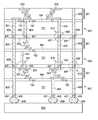
- FIG. 5illustrates an embodiment of the present invention in which a first die 501 formed using the process described above with respect to FIGS. 1-4 is integrated within a SiP architecture along with a packaging substrate 503 , a second die 505 , and a third die 507 .
- the packaging substrate 503provides I/O, power and ground connectivity to the via-first TSVs 401 and the via-last TSVs 403 through contact bumps 509 .
- the packaging substrate 503may be a printed circuit board (PCB), IC package, or any other substrate that may be mounted while also transmitting signals, power and ground to the first die 501 , second die 505 , and third die 507 .
- PCBprinted circuit board
- the contact bumps 509may comprise a material such as tin, or other suitable materials, such as silver, lead-free tin, or copper.
- the contact bumps 509may be formed by initially forming a layer of tin through such commonly used methods such as evaporation, electroplating, printing, solder transfer, ball placement, etc., to a thickness of about 100 ⁇ m. Once a layer of tin has been formed on the structure, a reflow may be performed in order to shape the material into the desired bump shapes.
- the second die 505 and the third die 507may also be formed similarly to the first die 501 as described above with reference to FIG. 1-4 .
- both the second die 505 and the third die 507may comprise both via-first TSVs 401 , via-last TSVs 403 , and contact pads 203 .
- the via-first TSVs 401are located so as to provide connectivity to either a contact pad 203 (as illustrated by the first circled area 511 ) or else a via-last TSV 403 (as illustrated by the second circled area 513 ) of an adjacent die. Additionally, the via-last TSVs 403 are located so as to provide connectivity to either a contact pad 203 (as illustrated by the third circled area 515 ) or else another via-last TSV 403 (as illustrated by the fourth circled area 517 ).
- any suitable combination of dies(with any number of via-first TSVs 401 and via-last TSVs 403 supplying power and signal paths, including none), may be utilized while remaining within the scope of the present invention, and all of these combinations are fully intended to be included within the scope of the present invention.
- redistribution layers or interposers(not shown) may be formed or placed to ensure the proper alignment of connections (e.g., conductive layer 405 and ENIG layer 407 ) between the first die 501 , the second die 505 , and the third die 507 .
- via-first TSVs 401 and via-last TSVs 403By using a combination of via-first TSVs 401 and via-last TSVs 403 , the advantages of both via-first TSVs 401 and via-last TSVs 403 may be utilized to provide a low resistive path for adjacent die connections through a via-first TSV 401 while also providing a feedthrough channel for multiple die connections through a via-last TSV 403 . By providing an appropriate TSV depending upon the precise usage of the TSV, the overall resistance of the interconnects may be reduced.
- Ris the resistance of the metallization layers in each die
- R′is the resistance of the via-first TSVs in each die
- R′′is the resistance of the via-last TSVs in each die
- the resistive path to one of the active devices 102 on the third die 507would be the resistance of a via-first TSV 401 in the third die 507 along with the resistances of the two via-last TSVs 403 that extend through the first die 501 and the second die 505 .
Landscapes
- Engineering & Computer Science (AREA)
- Microelectronics & Electronic Packaging (AREA)
- Power Engineering (AREA)
- Computer Hardware Design (AREA)
- Physics & Mathematics (AREA)
- Condensed Matter Physics & Semiconductors (AREA)
- General Physics & Mathematics (AREA)
- Manufacturing & Machinery (AREA)
- Internal Circuitry In Semiconductor Integrated Circuit Devices (AREA)
Abstract
Description
This application claims the benefit of U.S. Provisional Patent Application Ser. No. 61/158,260, filed on Mar. 6, 2009, and entitled “Three-Dimensional System-in-Package Architecture,” which application is incorporated herein by reference.
The present invention relates generally to a system and method for connecting semiconductor devices and, more particularly, to a system and method for using via-first through-silicon vias (TSVs) and via-last TSVs to connect dies in a System in Package (SiP) configuration.
Generally, through-silicon vias (TSVs) have been used to form electrical connections within System-in-Package (SiP) architectures to connect multiple semiconductor dies through the semiconductor die substrates. One method of forming these TSVs is known as a via-first method, in which the TSV is formed through the substrate prior to the formation of the semiconductor die's metallization layers, and the TSV is electrically connected to a metallization layer close to the substrate. However, while maintaining a low resistance path for connections to the active devices located on the substrate, such a connection actually increases the resistance of any feedthrough connections (e.g., for supplying power to another die), which must also include the resistance of the metallization layers through which the electricity must pass to get to the other side of the die.
To reduce this feedthrough resistance, another approach known as a via-last method may be used. In this method the metallization layers are formed over the substrate first, and the TSV is formed to extend through both the substrate and the metallization layers. This approach allows for a straight path through the die without the added resistance from the metallization layers. However, while reducing the resistance from one side of the die to the other side (and to other dies), such a TSV also increases the resistance to the active devices on the die in which it is located, as any electrical signal would have to travel all the way through the semiconductor die along the via-last TSV and then, additionally, travel back through the metallization layers in order to reach the active devices.
Therefore, what is needed is a system that can reduce the feedthrough resistance without increasing the resistance for connections to the active devices.
These and other problems are generally solved or circumvented, and technical advantages are generally achieved, by embodiments of the present invention which provide for a hybrid structure of through-silicon vias (TSVs) in a System in Package (SiP) architecture.
In accordance with an embodiment of the present invention, a semiconductor device comprises a substrate with a first side and a second side opposite the first side and a first conductive region located over the first side of the substrate. A first conductive via extends from the second side of the substrate to the first conductive region without extending through the first conductive region, and a second conductive via extends from the second side of the substrate through the first conductive region.
In accordance with another embodiment of the present invention, a semiconductor device comprises a first semiconductor die comprising a first substrate and a first metallization region, the first substrate comprising a first side and a second side. A first conductive via extends from the second side of the first substrate to the first side of the first substrate and terminates at the first metallization region. A second conductive via extends through the first semiconductor die.
In accordance with yet another embodiment of the present invention, a method of manufacturing a semiconductor device comprises providing a first substrate and forming a first conductive via through the first substrate. A first conductive region is formed over the first substrate, and a second conductive via is formed through both the first substrate and the first conductive region.
An advantage of an embodiment of the present invention is that it provides a low resistive path for adjacent die connections through a via-first TSV while also providing a feedthrough channel for multiple die connections through a via-last TSV. By providing different TSVs depending upon the precise usage of the TSV, the overall resistance of the interconnects may be reduced.
For a more complete understanding of the present invention, and the advantages thereof, reference is now made to the following descriptions taken in conjunction with the accompanying drawings, in which:
Corresponding numerals and symbols in the different figures generally refer to corresponding parts unless otherwise indicated. The figures are drawn to clearly illustrate the relevant aspects of the embodiments and are not necessarily drawn to scale.
The making and using of embodiments of the present invention are discussed in detail below. It should be appreciated, however, that the present invention provides many applicable inventive concepts that can be embodied in a wide variety of specific contexts. The specific embodiments discussed are merely illustrative of specific ways to make and use the invention, and do not limit the scope of the invention.
The present invention will be described with respect to embodiments of the present invention in a specific context, namely a three dimensional System-in-Package (SiP) architecture with a hybrid structure of via-first through-silicon vias (TSVs) and via-last TSVs. The invention may also be applied, however, to other types of electrical connections.
With reference now toFIG. 1 , there is shown asubstrate 101 withactive devices 102 and an interlayer dielectric (ILD)104, the substrate having afirst side 105, asecond side 107 opposite thefirst side 105, and a via-first TSV via103 formed therein. Thesubstrate 101 may comprise bulk silicon, doped or undoped, or an active layer of a silicon-on-insulator (SOI) substrate. Generally, an SOI substrate comprises a layer of a semiconductor material such as silicon, germanium, silicon germanium, SOI, silicon germanium-on-insulator (SGOI), or combinations thereof. Other substrates that may be used include multi-layered substrates, gradient substrates, or hybrid orientation substrates.
Theactive devices 102 are represented onFIG. 1 as two transistors. However, as one of skill in the art will recognize, a wide variety of active devices such as capacitors, resistors, inductors, high-k metal gate devices, and the like may be used to generate the desired structural and functional requirements of the design. Theactive devices 102 may be formed using any suitable methods either within or on the surface of thesubstrate 101.
The ILD104 is formed over thesubstrate 101 andactive devices 102 by chemical vapor deposition, sputtering, or any other method known and used in the art for forming anILD 104. The ILD104 typically may have a planarized surface and may be comprised of silicon oxide, although other materials, such as high-k materials, could alternatively be utilized. Optionally, the ILD104 may be formed so as to impart a strain to thesubstrate 101 within theactive devices 102, which will increase the overall performance of theactive devices 102, as is known in the art.
The via-first TSV via103 may be formed by initially applying and developing a suitable photoresist (not shown), and then etching the ILD104 andsubstrate 101 to form an opening. The opening at this stage is formed so as to extend into thesubstrate 101 at least further than theactive devices 102, and to a depth at least greater than the eventual desired thickness of the finishedsubstrate 101. Accordingly, while the depth is dependent upon the overall design of thefirst substrate 101, the depth may be between about 1 μm and about 700 μm below the surface of thesubstrate 101, such as about 50 μm. The opening also may be formed to have a diameter of between about 1 μm and about 100 μm, such as about 6 μm.
Once the opening has been formed, the opening may be filled with a barrier layer and a conductive material to form the via-first TSV via103. The barrier layer may comprise a conductive material such as titanium nitride, although other materials, such as tantalum nitride, titanium, a dielectric, or the like may alternatively be utilized. The barrier layer may be formed using a CVD process, such as PECVD. However, other alternative processes, such as sputtering or metal organic chemical vapor deposition (MOCVD), may alternatively be used. The barrier layer is formed so as to contour to the underlying shape of the opening for the via-first TSV via103.
The conductive material may comprise copper, although other suitable materials such as aluminum, alloys, doped polysilicon, combinations thereof, and the like, may alternatively be utilized. The conductive material may be formed by depositing a seed layer and then electroplating copper onto the seed layer, filling and overfilling the opening for the via-first TSV via103. Once the opening for the via-first TSV via103 has been filled, excess barrier layer and excess conductive material outside of the opening for the via-first TSV via103 is removed through a grinding process such as chemical mechanical polishing (CMP), although any suitable removal process may be used.
Contactpads 203 may be formed within the upper layer of the metallization layers201 in order to provide a connection from the circuitry (including theactive devices 102 and the metallization layers201) to other devices (such as other semiconductor dies as described below with respect toFIG. 5 ). Thecontact pads 203 may comprise aluminum, and may be formed by conformally depositing a layer of aluminum so as to contact a connection from lower layers of the metallization layers201. Once the layer of aluminum has been deposited, a photoresist may then be formed over the layer, and the layer of aluminum is then etched to form thecontact pads 203.
Optionally, via-last contact pads (not shown) may also be formed over the via-last TSV vias301 in order to provide for an exterior connection to other devices. The via-last contact pads may formed in a similar manner and from similar materials as thecontact pads 203 described above with respect toFIG. 2 . However, any suitable material and method to form the via-last contact pads may alternatively be utilized.
However, as one of ordinary skill in the art will recognize, the above described methods of forming the via-first TSV 401 and the via-last TSVs 403 are merely one illustrative embodiment, and are not intended to limit the present invention to just these methods. Other suitable methods may alternatively be utilized. For example, the openings for the via-first TSV via103 and the via-last TSV via301 may be filled with dielectric material until after the thinning of thesecond side 107 of thesubstrate 101, at which point the dielectric material may be removed and replaced with conductive material. This embodiment, and any other suitable embodiment, may alternatively be used to form the via-first TSV 401 and the via-last TSVs 403.
After the removal of a portion of thesecond side 107 of thesubstrate 101, a cleaning etch may be performed. This cleaning etch is intended to clean and polish thesubstrate 101 after the CMP. Additionally, this cleaning etch also helps release stresses that may have formed during the CMP process of grinding thesubstrate 101. The cleaning etch may use HNO3, although other suitable etchants may alternatively be used.
Furthermore, after a cleaning process to remove any remaining polishing residue such as copper oxide, aconductive layer 405 may be formed on thesecond side 107 of thesubstrate 101 in electrical contact with the via-first TSV 401 and the via-last TSVs 403. Theconductive layer 405 may comprise aluminum, and may be formed through a sputter deposition process. However, other materials, such as nickel or copper, and other formation processes, such as electroplating or electroless plating, may alternatively be used. Theconductive layer 405 may be formed with a thickness of between about 1 μm and about 3 μm, such as about 2 μm.
The formation of theconductive layer 405 may be followed by an Electroless Nickel Gold (ENIG) process to form anENIG layer 407 opposite theconductive layer 405 from thesubstrate 101. The ENIG process provides for a uniform metal surface finish for the formation of contacts from thesubstrate 101 to other devices (described below with respect toFIG. 5 ). The ENIG process may comprise cleaning theconductive layer 405, immersing thesubstrate 101 in a zincate activation solution, electrolessly plating nickel onto theconductive layer 405, and electrolessly plating gold onto the nickel. TheENIG layer 407 may be formed to a thickness of between about 2 μm and about 4 μm, such as about 3 μm. Once formed, theconductive layer 405 and theENIG layer 407 are patterned by a suitable photolithographic process and unwanted material is removed through a suitable etching process as illustrated byFIG. 4 .
It should be noted that theconductive layer 405 andENIG layer 407 described above are merely one potential process that may be used along the thinnedsecond side 107 of thesubstrate 101. Alternatively, thesecond side 107 of thesubstrate 101 may be recessed such that the via-first TSV 401 and the via-last TSVs 403 extend away from the surface of thesecond side 107 of thesubstrate 101. Additionally, a passivation layer may be formed in order to protect the via-first TSVs 401 or the via-last TSVs 403, or a redistribution layer or other types of suitable interconnects may alternatively be formed on thesecond side 107 of thesubstrate 101.
The contact bumps509 may comprise a material such as tin, or other suitable materials, such as silver, lead-free tin, or copper. In an embodiment in which the contact bumps509 are tin solder bumps, the contact bumps509 may be formed by initially forming a layer of tin through such commonly used methods such as evaporation, electroplating, printing, solder transfer, ball placement, etc., to a thickness of about 100 μm. Once a layer of tin has been formed on the structure, a reflow may be performed in order to shape the material into the desired bump shapes.
Thesecond die 505 and thethird die 507 may also be formed similarly to thefirst die 501 as described above with reference toFIG. 1-4 . For example, in this embodiment both thesecond die 505 and thethird die 507 may comprise both via-first TSVs 401, via-last TSVs 403, andcontact pads 203. Further, while the exact number, placement, and location of the via-first TSVs 401 and the via-last TSVs 403 will necessarily be dependent at least in part upon the overall design of the SiP, the via-first TSVs 401 are located so as to provide connectivity to either a contact pad203 (as illustrated by the first circled area511) or else a via-last TSV403 (as illustrated by the second circled area513) of an adjacent die. Additionally, the via-last TSVs 403 are located so as to provide connectivity to either a contact pad203 (as illustrated by the third circled area515) or else another via-last TSV403 (as illustrated by the fourth circled area517).
However, as one of ordinary skill in the art will recognize, there are many combinations that may be used to interconnect any number of suitable dies, and the above described embodiment is not intended to limit the present invention. Any suitable combination of dies (with any number of via-first TSVs 401 and via-last TSVs 403 supplying power and signal paths, including none), may be utilized while remaining within the scope of the present invention, and all of these combinations are fully intended to be included within the scope of the present invention. Additionally, redistribution layers or interposers (not shown) may be formed or placed to ensure the proper alignment of connections (e.g.,conductive layer 405 and ENIG layer407) between thefirst die 501, thesecond die 505, and thethird die 507.
By using a combination of via-first TSVs 401 and via-last TSVs 403, the advantages of both via-first TSVs 401 and via-last TSVs 403 may be utilized to provide a low resistive path for adjacent die connections through a via-first TSV 401 while also providing a feedthrough channel for multiple die connections through a via-last TSV 403. By providing an appropriate TSV depending upon the precise usage of the TSV, the overall resistance of the interconnects may be reduced.
For example, the resistance of an interconnect path between thepackaging substrate 503 to one of theactive devices 102 within thethird die 507 of an SiP such as the one illustrated inFIG. 5 containing both via-first TSVs 401 and via-last TSVs 403 may be calculated by Equation 1:
Interconnect Resistance=R′+(n−1)R″ (1)
Where: n is the number of dies
Interconnect Resistance=R′+(n−1)R″ (1)
Where: n is the number of dies
R is the resistance of the metallization layers in each die
R′ is the resistance of the via-first TSVs in each die
R″ is the resistance of the via-last TSVs in each die
In other words, the resistive path to one of theactive devices 102 on thethird die 507 would be the resistance of a via-first TSV 401 in thethird die 507 along with the resistances of the two via-last TSVs 403 that extend through thefirst die 501 and thesecond die 505.
This provides for a more cost effective solution for 3D SiP architecture than the standard prior art architectures that provide for connections to one of theactive devices 102 on thethird die 507 through either via-first TSVs 401 or via-last TSVs 403 only. In the case of only via-first TSVs 401, to get to anactive device 102 on thethird die 507, the resistive path would comprise the resistances of the via-first TSV 401 of thefirst die 501, themetallization layer 201 of thefirst die 501, the via-first TSV 401 of thesecond die 505, themetallization layer 201 of thesecond die 505, and the via-first TSV 401 of thethird die 507, as summarized in Equation 2:
Via-First TSV Resistance=(n−1)R+nR′ (2)
In the case of only via-last TSVs 403, the resistive path to get to one of theactive devices 102 on thethird die 507 would comprise the resistance through the via-last TSVs 403 of each of thefirst die 501, thesecond die 505, and thethird die 507, along with the resistance of themetallization layer 201 of thethird die 507, as summarized in Equation 3:
Via-Last TSV Resistance=(R+nR″ (3)
Via-First TSV Resistance=(n−1)R+nR′ (2)
In the case of only via-
Via-Last TSV Resistance=(R+nR″ (3)
Although the present invention and its advantages have been described in detail, it should be understood that various changes, substitutions and alterations can be made herein without departing from the spirit and scope of the invention as defined by the appended claims. For example, different combinations of via-first TSVs and via-last TSVs may be used in order to connect separate dies together. As another example, any number of methods used to form the via-first TSVs and via-last TSVs may alternatively be utilized.
Moreover, the scope of the present application is not intended to be limited to the particular embodiments of the process, machine, manufacture, composition of matter, means, methods and steps described in the specification. As one of ordinary skill in the art will readily appreciate from the disclosure of the present invention, processes, machines, manufacture, compositions of matter, means, methods, or steps, presently existing or later to be developed, that perform substantially the same function or achieve substantially the same result as the corresponding embodiments described herein may be utilized according to the present invention. Accordingly, the appended claims are intended to include within their scope such processes, machines, manufacture, compositions of matter, means, methods, or steps.
Claims (13)
1. A semiconductor device comprising:
a first substrate of a semiconductor die;
a first plurality of dielectric layers over a first side of the first substrate;
a first via extending through the first substrate and one or more of the first plurality of dielectric layers, the first via terminating in contact with a metal line of the semiconductor die; and
a second via extending through the first substrate and two or more of the first plurality of dielectric layers, the second via extending through more of the first plurality of dielectric layers than the first via and having a first end terminating at a first side of the semiconductor die and a second end terminating at a second side of the semiconductor die.
2. The semiconductor device ofclaim 1 , wherein the first via extends through only one of the first plurality of dielectric layers.
3. The semiconductor device ofclaim 1 , further comprising:
an active device located on the first substrate; and
a plurality of metallization layers over the active device, wherein a first metallization layer closest to the first substrate electrically connects the first via to the active device.
4. The semiconductor device ofclaim 3 , further comprising a conductive layer on an opposite side of the first substrate than the active device, the conductive layer in electrical contact with the first via.
5. The semiconductor device ofclaim 1 , wherein the second via extends through each of the first plurality of dielectric layers.
6. The semiconductor device ofclaim 1 , further comprising:
a second substrate;
a second plurality of dielectric layers;
a third via extending through the second substrate and one or more of the second plurality of dielectric layers; and
a fourth via extending through the second substrate and two or more of the second plurality of dielectric layers, the fourth via extending through more of the second plurality of dielectric layers than the third via, wherein the fourth via is electrically connected to the second via.
7. The semiconductor device ofclaim 6 , wherein the third via is electrically connected to the first via through metallization layers located within the first plurality of dielectric layers.
8. A semiconductor device comprising:
a first semiconductor die comprising a first substrate;
a first conductive via extending through the first semiconductor die but not extending beyond the semiconductor die; and
a second conductive via extending partially through the first semiconductor die, the second conductive via extending through the first substrate and having a first end in physical contact with a conductive portion of a metallization layer of the semiconductor die, the metallization layer being electrically connected to both an active device of the first semiconductor die and a contact pad of the first semiconductor die, the contact pad being on a same side of the first semiconductor die as the active device.
9. The semiconductor device ofclaim 8 , further comprising a plurality of dielectric layers over the first substrate, wherein the second conductive via extends through a single dielectric layer located adjacent to the first substrate.
10. The semiconductor device ofclaim 8 , further comprising an active device on the first substrate, wherein the active device is electrically connected to the second conductive via through the metallization layer.
11. The semiconductor device ofclaim 10 , wherein the first conductive via is surrounded by dielectric material through the semiconductor die.
12. The semiconductor device ofclaim 8 , further comprising:
a second semiconductor die comprising a second substrate;
a third conductive via extending through the second semiconductor die, wherein the third conductive via is electrically connected to the second conductive via; and
a fourth conductive via extending less than through the second semiconductor die, the fourth conductive via extending through the second substrate.
13. The semiconductor device ofclaim 12 , wherein the third conductive via is electrically connected to the second conductive via through metallization layers located over the substrate in the first semiconductor die.
Priority Applications (6)
| Application Number | Priority Date | Filing Date | Title |
|---|---|---|---|
| US12/631,346US8487444B2 (en) | 2009-03-06 | 2009-12-04 | Three-dimensional system-in-package architecture |
| TW99105432ATWI416693B (en) | 2009-03-06 | 2010-02-25 | Semiconductor devices and fabrication methods thereof |
| KR1020100018037AKR20100100629A (en) | 2009-03-06 | 2010-02-26 | Three-dimensional system-in-package architecture |
| CN2010101302157ACN101840912B (en) | 2009-03-06 | 2010-03-05 | Semiconductor device and manufacturing method thereof |
| JP2010049223AJP2010219526A (en) | 2009-03-06 | 2010-03-05 | Semiconductor device, and manufacturing method of semiconductor device |
| US13/864,112US9099540B2 (en) | 2009-03-06 | 2013-04-16 | Three-dimensional system-in-package architecture |
Applications Claiming Priority (2)
| Application Number | Priority Date | Filing Date | Title |
|---|---|---|---|
| US15826009P | 2009-03-06 | 2009-03-06 | |
| US12/631,346US8487444B2 (en) | 2009-03-06 | 2009-12-04 | Three-dimensional system-in-package architecture |
Related Child Applications (1)
| Application Number | Title | Priority Date | Filing Date |
|---|---|---|---|
| US13/864,112DivisionUS9099540B2 (en) | 2009-03-06 | 2013-04-16 | Three-dimensional system-in-package architecture |
Publications (2)
| Publication Number | Publication Date |
|---|---|
| US20100225002A1 US20100225002A1 (en) | 2010-09-09 |
| US8487444B2true US8487444B2 (en) | 2013-07-16 |
Family
ID=42677503
Family Applications (2)
| Application Number | Title | Priority Date | Filing Date |
|---|---|---|---|
| US12/631,346Active2030-04-19US8487444B2 (en) | 2009-03-06 | 2009-12-04 | Three-dimensional system-in-package architecture |
| US13/864,112ActiveUS9099540B2 (en) | 2009-03-06 | 2013-04-16 | Three-dimensional system-in-package architecture |
Family Applications After (1)
| Application Number | Title | Priority Date | Filing Date |
|---|---|---|---|
| US13/864,112ActiveUS9099540B2 (en) | 2009-03-06 | 2013-04-16 | Three-dimensional system-in-package architecture |
Country Status (5)
| Country | Link |
|---|---|
| US (2) | US8487444B2 (en) |
| JP (1) | JP2010219526A (en) |
| KR (1) | KR20100100629A (en) |
| CN (1) | CN101840912B (en) |
| TW (1) | TWI416693B (en) |
Cited By (31)
| Publication number | Priority date | Publication date | Assignee | Title |
|---|---|---|---|---|
| US20100171203A1 (en)* | 2009-01-07 | 2010-07-08 | Taiwan Semiconductor Manufacturing Company | Robust TSV structure |
| US20110108947A1 (en)* | 2009-11-12 | 2011-05-12 | Guzek John S | Microelectronic device and method of manufacturing same |
| US20120206954A1 (en)* | 2011-02-15 | 2012-08-16 | Renesas Electronics Corporation | Semiconductor device and electronic device |
| US20130285236A1 (en)* | 2009-03-26 | 2013-10-31 | Stats Chippac, Ltd. | Semiconductor Device and Method of Forming a Thin Wafer Without a Carrier |
| US9309106B2 (en) | 2013-07-08 | 2016-04-12 | Motion Engine Inc. | 3D MEMS device and method of manufacturing |
| US9780075B2 (en) | 2014-08-11 | 2017-10-03 | Massachusetts Institute Of Technology | Interconnect structures for assembly of multi-layer semiconductor devices |
| US9786633B2 (en) | 2014-04-23 | 2017-10-10 | Massachusetts Institute Of Technology | Interconnect structures for fine pitch assembly of semiconductor structures and related techniques |
| US9812429B2 (en) | 2014-11-05 | 2017-11-07 | Massachusetts Institute Of Technology | Interconnect structures for assembly of multi-layer semiconductor devices |
| US9905535B2 (en) | 2014-11-21 | 2018-02-27 | Samsung Electronics Co., Ltd. | Semiconductor packages and fabrication method thereof |
| WO2018056965A1 (en)* | 2016-09-21 | 2018-03-29 | Massachusetts Institute Of Technology | Multi-layer semiconductor structure and methods for fabricating multi-layer semiconductor structures |
| US20180218973A1 (en)* | 2015-09-25 | 2018-08-02 | Intel Corporation | Metal on both sides with power distributed through the silicon |
| US10121754B2 (en) | 2015-11-05 | 2018-11-06 | Massachusetts Institute Of Technology | Interconnect structures and methods for fabricating interconnect structures |
| US10134972B2 (en) | 2015-07-23 | 2018-11-20 | Massachusetts Institute Of Technology | Qubit and coupler circuit structures and coupling techniques |
| US10214414B2 (en) | 2014-01-09 | 2019-02-26 | Motion Engine, Inc. | Integrated MEMS system |
| US10242968B2 (en) | 2015-11-05 | 2019-03-26 | Massachusetts Institute Of Technology | Interconnect structure and semiconductor structures for assembly of cryogenic electronic packages |
| US10273147B2 (en) | 2013-07-08 | 2019-04-30 | Motion Engine Inc. | MEMS components and method of wafer-level manufacturing thereof |
| US10325873B2 (en)* | 2017-07-21 | 2019-06-18 | United Microelectronics Corp. | Chip-stack structure |
| US10381541B2 (en) | 2016-10-11 | 2019-08-13 | Massachusetts Institute Of Technology | Cryogenic electronic packages and methods for fabricating cryogenic electronic packages |
| US10407299B2 (en) | 2015-01-15 | 2019-09-10 | Motion Engine Inc. | 3D MEMS device with hermetic cavity |
| US10658424B2 (en) | 2015-07-23 | 2020-05-19 | Massachusetts Institute Of Technology | Superconducting integrated circuit |
| US20200241071A1 (en)* | 2019-01-25 | 2020-07-30 | Texas Instruments Incorporated | In-wafer reliability testing |
| US10769546B1 (en) | 2015-04-27 | 2020-09-08 | Rigetti & Co, Inc. | Microwave integrated quantum circuits with cap wafer and methods for making the same |
| US10768065B2 (en) | 2014-04-10 | 2020-09-08 | Mei Micro, Inc. | MEMS pressure sensor |
| US11287486B2 (en) | 2014-12-09 | 2022-03-29 | Motion Engine, Inc. | 3D MEMS magnetometer and associated methods |
| US20220310485A1 (en)* | 2021-03-24 | 2022-09-29 | Samsung Electronics Co., Ltd. | Semiconductor device including through via structure |
| US20220336326A1 (en)* | 2021-04-16 | 2022-10-20 | Samsung Electronics Co., Ltd. | Semiconductor chip and semiconductor package including same |
| US11674803B2 (en) | 2014-06-02 | 2023-06-13 | Motion Engine, Inc. | Multi-mass MEMS motion sensor |
| US11770982B1 (en) | 2017-06-19 | 2023-09-26 | Rigetti & Co, Llc | Microwave integrated quantum circuits with cap wafers and their methods of manufacture |
| US11804419B2 (en) | 2020-07-31 | 2023-10-31 | Samsung Electronics Co., Ltd. | Semiconductor device |
| US11852481B2 (en) | 2013-08-02 | 2023-12-26 | Motion Engine Inc. | MEMS motion sensor and method of manufacturing |
| US12001772B2 (en) | 2021-09-24 | 2024-06-04 | International Business Machines Corporation | Ultra-short-height standard cell architecture |
Families Citing this family (246)
| Publication number | Priority date | Publication date | Assignee | Title |
|---|---|---|---|---|
| US9064717B2 (en)* | 2008-09-26 | 2015-06-23 | International Business Machines Corporation | Lock and key through-via method for wafer level 3D integration and structures produced thereby |
| US8487444B2 (en) | 2009-03-06 | 2013-07-16 | Taiwan Semiconductor Manufacturing Company, Ltd. | Three-dimensional system-in-package architecture |
| US8362482B2 (en) | 2009-04-14 | 2013-01-29 | Monolithic 3D Inc. | Semiconductor device and structure |
| US7964916B2 (en)* | 2009-04-14 | 2011-06-21 | Monolithic 3D Inc. | Method for fabrication of a semiconductor device and structure |
| US9577642B2 (en) | 2009-04-14 | 2017-02-21 | Monolithic 3D Inc. | Method to form a 3D semiconductor device |
| US8669778B1 (en) | 2009-04-14 | 2014-03-11 | Monolithic 3D Inc. | Method for design and manufacturing of a 3D semiconductor device |
| US8058137B1 (en) | 2009-04-14 | 2011-11-15 | Monolithic 3D Inc. | Method for fabrication of a semiconductor device and structure |
| US8395191B2 (en) | 2009-10-12 | 2013-03-12 | Monolithic 3D Inc. | Semiconductor device and structure |
| US9509313B2 (en) | 2009-04-14 | 2016-11-29 | Monolithic 3D Inc. | 3D semiconductor device |
| US8367470B2 (en)* | 2009-08-07 | 2013-02-05 | Stats Chippac, Ltd. | Semiconductor device and method of forming cavity in build-up interconnect structure for short signal path between die |
| US10043781B2 (en) | 2009-10-12 | 2018-08-07 | Monolithic 3D Inc. | 3D semiconductor device and structure |
| US12027518B1 (en) | 2009-10-12 | 2024-07-02 | Monolithic 3D Inc. | 3D semiconductor devices and structures with metal layers |
| US11374118B2 (en) | 2009-10-12 | 2022-06-28 | Monolithic 3D Inc. | Method to form a 3D integrated circuit |
| US10157909B2 (en) | 2009-10-12 | 2018-12-18 | Monolithic 3D Inc. | 3D semiconductor device and structure |
| US11018133B2 (en) | 2009-10-12 | 2021-05-25 | Monolithic 3D Inc. | 3D integrated circuit |
| US11984445B2 (en) | 2009-10-12 | 2024-05-14 | Monolithic 3D Inc. | 3D semiconductor devices and structures with metal layers |
| US10354995B2 (en) | 2009-10-12 | 2019-07-16 | Monolithic 3D Inc. | Semiconductor memory device and structure |
| US10388863B2 (en) | 2009-10-12 | 2019-08-20 | Monolithic 3D Inc. | 3D memory device and structure |
| US9892972B2 (en)* | 2009-10-12 | 2018-02-13 | Monolithic 3D Inc. | 3D semiconductor device and structure |
| US10366970B2 (en) | 2009-10-12 | 2019-07-30 | Monolithic 3D Inc. | 3D semiconductor device and structure |
| US10910364B2 (en) | 2009-10-12 | 2021-02-02 | Monolitaic 3D Inc. | 3D semiconductor device |
| US9099424B1 (en) | 2012-08-10 | 2015-08-04 | Monolithic 3D Inc. | Semiconductor system, device and structure with heat removal |
| US9099526B2 (en) | 2010-02-16 | 2015-08-04 | Monolithic 3D Inc. | Integrated circuit device and structure |
| US8026521B1 (en) | 2010-10-11 | 2011-09-27 | Monolithic 3D Inc. | Semiconductor device and structure |
| US8143712B2 (en)* | 2010-07-15 | 2012-03-27 | Nanya Technology Corp. | Die package structure |
| US9219005B2 (en) | 2011-06-28 | 2015-12-22 | Monolithic 3D Inc. | Semiconductor system and device |
| US9953925B2 (en) | 2011-06-28 | 2018-04-24 | Monolithic 3D Inc. | Semiconductor system and device |
| US10217667B2 (en) | 2011-06-28 | 2019-02-26 | Monolithic 3D Inc. | 3D semiconductor device, fabrication method and system |
| KR20120012602A (en)* | 2010-08-02 | 2012-02-10 | 삼성전자주식회사 | Semiconductor device, manufacturing method thereof and manufacturing method of semiconductor package |
| KR101190682B1 (en) | 2010-09-30 | 2012-10-12 | 에스케이하이닉스 주식회사 | Three dimensional stacked semiconductor integrated circuit |
| US12362219B2 (en) | 2010-11-18 | 2025-07-15 | Monolithic 3D Inc. | 3D semiconductor memory device and structure |
| US10497713B2 (en) | 2010-11-18 | 2019-12-03 | Monolithic 3D Inc. | 3D semiconductor memory device and structure |
| US8273610B2 (en) | 2010-11-18 | 2012-09-25 | Monolithic 3D Inc. | Method of constructing a semiconductor device and structure |
| US8163581B1 (en) | 2010-10-13 | 2012-04-24 | Monolith IC 3D | Semiconductor and optoelectronic devices |
| US11482440B2 (en) | 2010-12-16 | 2022-10-25 | Monolithic 3D Inc. | 3D semiconductor device and structure with a built-in test circuit for repairing faulty circuits |
| US10896931B1 (en) | 2010-10-11 | 2021-01-19 | Monolithic 3D Inc. | 3D semiconductor device and structure |
| US11257867B1 (en) | 2010-10-11 | 2022-02-22 | Monolithic 3D Inc. | 3D semiconductor device and structure with oxide bonds |
| US11024673B1 (en) | 2010-10-11 | 2021-06-01 | Monolithic 3D Inc. | 3D semiconductor device and structure |
| US11158674B2 (en) | 2010-10-11 | 2021-10-26 | Monolithic 3D Inc. | Method to produce a 3D semiconductor device and structure |
| US11600667B1 (en) | 2010-10-11 | 2023-03-07 | Monolithic 3D Inc. | Method to produce 3D semiconductor devices and structures with memory |
| US11018191B1 (en) | 2010-10-11 | 2021-05-25 | Monolithic 3D Inc. | 3D semiconductor device and structure |
| US11469271B2 (en) | 2010-10-11 | 2022-10-11 | Monolithic 3D Inc. | Method to produce 3D semiconductor devices and structures with memory |
| US11315980B1 (en) | 2010-10-11 | 2022-04-26 | Monolithic 3D Inc. | 3D semiconductor device and structure with transistors |
| US11227897B2 (en) | 2010-10-11 | 2022-01-18 | Monolithic 3D Inc. | Method for producing a 3D semiconductor memory device and structure |
| US10290682B2 (en) | 2010-10-11 | 2019-05-14 | Monolithic 3D Inc. | 3D IC semiconductor device and structure with stacked memory |
| US10833108B2 (en) | 2010-10-13 | 2020-11-10 | Monolithic 3D Inc. | 3D microdisplay device and structure |
| US11163112B2 (en) | 2010-10-13 | 2021-11-02 | Monolithic 3D Inc. | Multilevel semiconductor device and structure with electromagnetic modulators |
| US11404466B2 (en) | 2010-10-13 | 2022-08-02 | Monolithic 3D Inc. | Multilevel semiconductor device and structure with image sensors |
| US12360310B2 (en) | 2010-10-13 | 2025-07-15 | Monolithic 3D Inc. | Multilevel semiconductor device and structure with oxide bonding |
| US11133344B2 (en) | 2010-10-13 | 2021-09-28 | Monolithic 3D Inc. | Multilevel semiconductor device and structure with image sensors |
| US10998374B1 (en) | 2010-10-13 | 2021-05-04 | Monolithic 3D Inc. | Multilevel semiconductor device and structure |
| US11605663B2 (en) | 2010-10-13 | 2023-03-14 | Monolithic 3D Inc. | Multilevel semiconductor device and structure with image sensors and wafer bonding |
| US11437368B2 (en) | 2010-10-13 | 2022-09-06 | Monolithic 3D Inc. | Multilevel semiconductor device and structure with oxide bonding |
| US10978501B1 (en) | 2010-10-13 | 2021-04-13 | Monolithic 3D Inc. | Multilevel semiconductor device and structure with waveguides |
| US9197804B1 (en) | 2011-10-14 | 2015-11-24 | Monolithic 3D Inc. | Semiconductor and optoelectronic devices |
| US12094892B2 (en) | 2010-10-13 | 2024-09-17 | Monolithic 3D Inc. | 3D micro display device and structure |
| US11164898B2 (en) | 2010-10-13 | 2021-11-02 | Monolithic 3D Inc. | Multilevel semiconductor device and structure |
| US10679977B2 (en) | 2010-10-13 | 2020-06-09 | Monolithic 3D Inc. | 3D microdisplay device and structure |
| US11063071B1 (en) | 2010-10-13 | 2021-07-13 | Monolithic 3D Inc. | Multilevel semiconductor device and structure with waveguides |
| US12080743B2 (en) | 2010-10-13 | 2024-09-03 | Monolithic 3D Inc. | Multilevel semiconductor device and structure with image sensors and wafer bonding |
| US11327227B2 (en) | 2010-10-13 | 2022-05-10 | Monolithic 3D Inc. | Multilevel semiconductor device and structure with electromagnetic modulators |
| US10943934B2 (en) | 2010-10-13 | 2021-03-09 | Monolithic 3D Inc. | Multilevel semiconductor device and structure |
| US11929372B2 (en) | 2010-10-13 | 2024-03-12 | Monolithic 3D Inc. | Multilevel semiconductor device and structure with image sensors and wafer bonding |
| US11984438B2 (en) | 2010-10-13 | 2024-05-14 | Monolithic 3D Inc. | Multilevel semiconductor device and structure with oxide bonding |
| US11855100B2 (en) | 2010-10-13 | 2023-12-26 | Monolithic 3D Inc. | Multilevel semiconductor device and structure with oxide bonding |
| US11869915B2 (en) | 2010-10-13 | 2024-01-09 | Monolithic 3D Inc. | Multilevel semiconductor device and structure with image sensors and wafer bonding |
| US11694922B2 (en) | 2010-10-13 | 2023-07-04 | Monolithic 3D Inc. | Multilevel semiconductor device and structure with oxide bonding |
| US11855114B2 (en) | 2010-10-13 | 2023-12-26 | Monolithic 3D Inc. | Multilevel semiconductor device and structure with image sensors and wafer bonding |
| US11043523B1 (en) | 2010-10-13 | 2021-06-22 | Monolithic 3D Inc. | Multilevel semiconductor device and structure with image sensors |
| KR101690487B1 (en)* | 2010-11-08 | 2016-12-28 | 삼성전자주식회사 | Semiconductor device and fabrication method thereof |
| US11923230B1 (en) | 2010-11-18 | 2024-03-05 | Monolithic 3D Inc. | 3D semiconductor device and structure with bonding |
| US11610802B2 (en) | 2010-11-18 | 2023-03-21 | Monolithic 3D Inc. | Method for producing a 3D semiconductor device and structure with single crystal transistors and metal gate electrodes |
| US11004719B1 (en) | 2010-11-18 | 2021-05-11 | Monolithic 3D Inc. | Methods for producing a 3D semiconductor memory device and structure |
| US11164770B1 (en) | 2010-11-18 | 2021-11-02 | Monolithic 3D Inc. | Method for producing a 3D semiconductor memory device and structure |
| US12100611B2 (en) | 2010-11-18 | 2024-09-24 | Monolithic 3D Inc. | Methods for producing a 3D semiconductor device and structure with memory cells and multiple metal layers |
| US12068187B2 (en) | 2010-11-18 | 2024-08-20 | Monolithic 3D Inc. | 3D semiconductor device and structure with bonding and DRAM memory cells |
| US11569117B2 (en) | 2010-11-18 | 2023-01-31 | Monolithic 3D Inc. | 3D semiconductor device and structure with single-crystal layers |
| US11482439B2 (en) | 2010-11-18 | 2022-10-25 | Monolithic 3D Inc. | Methods for producing a 3D semiconductor memory device comprising charge trap junction-less transistors |
| US11615977B2 (en) | 2010-11-18 | 2023-03-28 | Monolithic 3D Inc. | 3D semiconductor memory device and structure |
| US11107721B2 (en) | 2010-11-18 | 2021-08-31 | Monolithic 3D Inc. | 3D semiconductor device and structure with NAND logic |
| US11018042B1 (en) | 2010-11-18 | 2021-05-25 | Monolithic 3D Inc. | 3D semiconductor memory device and structure |
| US11862503B2 (en) | 2010-11-18 | 2024-01-02 | Monolithic 3D Inc. | Method for producing a 3D semiconductor device and structure with memory cells and multiple metal layers |
| US11804396B2 (en) | 2010-11-18 | 2023-10-31 | Monolithic 3D Inc. | Methods for producing a 3D semiconductor device and structure with memory cells and multiple metal layers |
| US11211279B2 (en) | 2010-11-18 | 2021-12-28 | Monolithic 3D Inc. | Method for processing a 3D integrated circuit and structure |
| US12136562B2 (en) | 2010-11-18 | 2024-11-05 | Monolithic 3D Inc. | 3D semiconductor device and structure with single-crystal layers |
| US11521888B2 (en) | 2010-11-18 | 2022-12-06 | Monolithic 3D Inc. | 3D semiconductor device and structure with high-k metal gate transistors |
| US11094576B1 (en) | 2010-11-18 | 2021-08-17 | Monolithic 3D Inc. | Methods for producing a 3D semiconductor memory device and structure |
| US11495484B2 (en) | 2010-11-18 | 2022-11-08 | Monolithic 3D Inc. | 3D semiconductor devices and structures with at least two single-crystal layers |
| US12243765B2 (en) | 2010-11-18 | 2025-03-04 | Monolithic 3D Inc. | 3D semiconductor device and structure with metal layers and memory cells |
| US11443971B2 (en) | 2010-11-18 | 2022-09-13 | Monolithic 3D Inc. | 3D semiconductor device and structure with memory |
| US11854857B1 (en) | 2010-11-18 | 2023-12-26 | Monolithic 3D Inc. | Methods for producing a 3D semiconductor device and structure with memory cells and multiple metal layers |
| US11735462B2 (en) | 2010-11-18 | 2023-08-22 | Monolithic 3D Inc. | 3D semiconductor device and structure with single-crystal layers |
| US11355381B2 (en) | 2010-11-18 | 2022-06-07 | Monolithic 3D Inc. | 3D semiconductor memory device and structure |
| US12154817B1 (en) | 2010-11-18 | 2024-11-26 | Monolithic 3D Inc. | Methods for producing a 3D semiconductor memory device and structure |
| US12125737B1 (en) | 2010-11-18 | 2024-10-22 | Monolithic 3D Inc. | 3D semiconductor device and structure with metal layers and memory cells |
| US11508605B2 (en) | 2010-11-18 | 2022-11-22 | Monolithic 3D Inc. | 3D semiconductor memory device and structure |
| US11031275B2 (en) | 2010-11-18 | 2021-06-08 | Monolithic 3D Inc. | 3D semiconductor device and structure with memory |
| US11355380B2 (en) | 2010-11-18 | 2022-06-07 | Monolithic 3D Inc. | Methods for producing 3D semiconductor memory device and structure utilizing alignment marks |
| US11121021B2 (en) | 2010-11-18 | 2021-09-14 | Monolithic 3D Inc. | 3D semiconductor device and structure |
| US12033884B2 (en) | 2010-11-18 | 2024-07-09 | Monolithic 3D Inc. | Methods for producing a 3D semiconductor device and structure with memory cells and multiple metal layers |
| US11784082B2 (en) | 2010-11-18 | 2023-10-10 | Monolithic 3D Inc. | 3D semiconductor device and structure with bonding |
| US12144190B2 (en) | 2010-11-18 | 2024-11-12 | Monolithic 3D Inc. | 3D semiconductor device and structure with bonding and memory cells preliminary class |
| US11482438B2 (en) | 2010-11-18 | 2022-10-25 | Monolithic 3D Inc. | Methods for producing a 3D semiconductor memory device and structure |
| US12272586B2 (en) | 2010-11-18 | 2025-04-08 | Monolithic 3D Inc. | 3D semiconductor memory device and structure with memory and metal layers |
| US11901210B2 (en) | 2010-11-18 | 2024-02-13 | Monolithic 3D Inc. | 3D semiconductor device and structure with memory |
| FR2969592B1 (en)* | 2010-12-23 | 2013-02-08 | Commissariat Energie Atomique | DEVICE FOR CONNECTING NANO-OBJECTS TO EXTERNAL ELECTRICAL SYSTEMS, AND METHOD FOR MANUFACTURING THE DEVICE |
| KR101209458B1 (en) | 2010-12-24 | 2012-12-07 | 한국과학기술원 | Semiconductor chip, method of manufacturing semiconductor chip and semiconductor module using the same |
| CN102543729B (en) | 2010-12-31 | 2014-03-12 | 中芯国际集成电路制造(上海)有限公司 | Forming method of capacitor and capacitor structure thereof |
| WO2012123839A1 (en) | 2011-03-11 | 2012-09-20 | Basf Se | Method for forming through-base wafer vias |
| TWI467695B (en)* | 2011-03-24 | 2015-01-01 | Sony Corp | Semiconductor device and method for manufacturing same |
| JP2012221998A (en) | 2011-04-04 | 2012-11-12 | Toshiba Corp | Semiconductor device and manufacturing method of the same |
| US10388568B2 (en) | 2011-06-28 | 2019-08-20 | Monolithic 3D Inc. | 3D semiconductor device and system |
| US8617925B2 (en)* | 2011-08-09 | 2013-12-31 | Soitec | Methods of forming bonded semiconductor structures in 3D integration processes using recoverable substrates, and bonded semiconductor structures formed by such methods |
| US8687399B2 (en) | 2011-10-02 | 2014-04-01 | Monolithic 3D Inc. | Semiconductor device and structure |
| CN103875072A (en)* | 2011-10-17 | 2014-06-18 | 松下电器产业株式会社 | Integrated circuit, multi-core processor device and method for manufacturing integrated circuit |
| US9142510B2 (en) | 2011-10-28 | 2015-09-22 | Intel Corporation | 3D interconnect structure comprising through-silicon vias combined with fine pitch backside metal redistribution lines fabricated using a dual damascene type approach |
| KR101620767B1 (en) | 2011-10-28 | 2016-05-12 | 인텔 코포레이션 | 3d interconnect structure comprising fine pitch single damascene backside metal redistribution lines combined with through-silicon vias |
| US9362267B2 (en)* | 2012-03-15 | 2016-06-07 | Infineon Technologies Americas Corp. | Group III-V and group IV composite switch |
| US11735501B1 (en) | 2012-04-09 | 2023-08-22 | Monolithic 3D Inc. | 3D semiconductor device and structure with metal layers and a connective path |
| US11881443B2 (en) | 2012-04-09 | 2024-01-23 | Monolithic 3D Inc. | 3D semiconductor device and structure with metal layers and a connective path |
| US11164811B2 (en) | 2012-04-09 | 2021-11-02 | Monolithic 3D Inc. | 3D semiconductor device with isolation layers and oxide-to-oxide bonding |
| US11594473B2 (en) | 2012-04-09 | 2023-02-28 | Monolithic 3D Inc. | 3D semiconductor device and structure with metal layers and a connective path |
| US11616004B1 (en) | 2012-04-09 | 2023-03-28 | Monolithic 3D Inc. | 3D semiconductor device and structure with metal layers and a connective path |
| US8557632B1 (en) | 2012-04-09 | 2013-10-15 | Monolithic 3D Inc. | Method for fabrication of a semiconductor device and structure |
| US11694944B1 (en) | 2012-04-09 | 2023-07-04 | Monolithic 3D Inc. | 3D semiconductor device and structure with metal layers and a connective path |
| US11410912B2 (en) | 2012-04-09 | 2022-08-09 | Monolithic 3D Inc. | 3D semiconductor device with vias and isolation layers |
| US11476181B1 (en) | 2012-04-09 | 2022-10-18 | Monolithic 3D Inc. | 3D semiconductor device and structure with metal layers |
| US11088050B2 (en) | 2012-04-09 | 2021-08-10 | Monolithic 3D Inc. | 3D semiconductor device with isolation layers |
| US10600888B2 (en) | 2012-04-09 | 2020-03-24 | Monolithic 3D Inc. | 3D semiconductor device |
| US9443783B2 (en)* | 2012-06-27 | 2016-09-13 | Taiwan Semiconductor Manufacturing Company, Ltd. | 3DIC stacking device and method of manufacture |
| US9817928B2 (en) | 2012-08-31 | 2017-11-14 | Synopsys, Inc. | Latch-up suppression and substrate noise coupling reduction through a substrate back-tie for 3D integrated circuits |
| US9190346B2 (en) | 2012-08-31 | 2015-11-17 | Synopsys, Inc. | Latch-up suppression and substrate noise coupling reduction through a substrate back-tie for 3D integrated circuits |
| KR101419601B1 (en) | 2012-11-20 | 2014-07-16 | 앰코 테크놀로지 코리아 주식회사 | Semiconductor device using epoxy molding compound wafer support system and fabricating method thereof |
| US8933564B2 (en) | 2012-12-21 | 2015-01-13 | Intel Corporation | Landing structure for through-silicon via |
| US11018116B2 (en) | 2012-12-22 | 2021-05-25 | Monolithic 3D Inc. | Method to form a 3D semiconductor device and structure |
| US8674470B1 (en) | 2012-12-22 | 2014-03-18 | Monolithic 3D Inc. | Semiconductor device and structure |
| US11309292B2 (en) | 2012-12-22 | 2022-04-19 | Monolithic 3D Inc. | 3D semiconductor device and structure with metal layers |
| US11217565B2 (en) | 2012-12-22 | 2022-01-04 | Monolithic 3D Inc. | Method to form a 3D semiconductor device and structure |
| US11961827B1 (en) | 2012-12-22 | 2024-04-16 | Monolithic 3D Inc. | 3D semiconductor device and structure with metal layers |
| US11784169B2 (en) | 2012-12-22 | 2023-10-10 | Monolithic 3D Inc. | 3D semiconductor device and structure with metal layers |
| US12051674B2 (en) | 2012-12-22 | 2024-07-30 | Monolithic 3D Inc. | 3D semiconductor device and structure with metal layers |
| US11063024B1 (en) | 2012-12-22 | 2021-07-13 | Monlithic 3D Inc. | Method to form a 3D semiconductor device and structure |
| US11967583B2 (en) | 2012-12-22 | 2024-04-23 | Monolithic 3D Inc. | 3D semiconductor device and structure with metal layers |
| US11916045B2 (en) | 2012-12-22 | 2024-02-27 | Monolithic 3D Inc. | 3D semiconductor device and structure with metal layers |
| US11087995B1 (en) | 2012-12-29 | 2021-08-10 | Monolithic 3D Inc. | 3D semiconductor device and structure |
| US11430668B2 (en) | 2012-12-29 | 2022-08-30 | Monolithic 3D Inc. | 3D semiconductor device and structure with bonding |
| US12249538B2 (en) | 2012-12-29 | 2025-03-11 | Monolithic 3D Inc. | 3D semiconductor device and structure including power distribution grids |
| US10903089B1 (en) | 2012-12-29 | 2021-01-26 | Monolithic 3D Inc. | 3D semiconductor device and structure |
| US10600657B2 (en) | 2012-12-29 | 2020-03-24 | Monolithic 3D Inc | 3D semiconductor device and structure |
| US9385058B1 (en) | 2012-12-29 | 2016-07-05 | Monolithic 3D Inc. | Semiconductor device and structure |
| US10892169B2 (en) | 2012-12-29 | 2021-01-12 | Monolithic 3D Inc. | 3D semiconductor device and structure |
| US11177140B2 (en) | 2012-12-29 | 2021-11-16 | Monolithic 3D Inc. | 3D semiconductor device and structure |
| US10115663B2 (en) | 2012-12-29 | 2018-10-30 | Monolithic 3D Inc. | 3D semiconductor device and structure |
| US11004694B1 (en) | 2012-12-29 | 2021-05-11 | Monolithic 3D Inc. | 3D semiconductor device and structure |
| US9871034B1 (en) | 2012-12-29 | 2018-01-16 | Monolithic 3D Inc. | Semiconductor device and structure |
| US11430667B2 (en) | 2012-12-29 | 2022-08-30 | Monolithic 3D Inc. | 3D semiconductor device and structure with bonding |
| US10651054B2 (en) | 2012-12-29 | 2020-05-12 | Monolithic 3D Inc. | 3D semiconductor device and structure |
| US9245790B2 (en)* | 2013-01-23 | 2016-01-26 | GlobalFoundries, Inc. | Integrated circuits and methods of forming the same with multiple embedded interconnect connection to same through-semiconductor via |
| CN103165561B (en)* | 2013-02-28 | 2015-09-23 | 江阴长电先进封装有限公司 | A kind of encapsulating structure of silicon substrate pinboard |
| US12094965B2 (en) | 2013-03-11 | 2024-09-17 | Monolithic 3D Inc. | 3D semiconductor device and structure with metal layers and memory cells |
| US8902663B1 (en) | 2013-03-11 | 2014-12-02 | Monolithic 3D Inc. | Method of maintaining a memory state |
| US10325651B2 (en) | 2013-03-11 | 2019-06-18 | Monolithic 3D Inc. | 3D semiconductor device with stacked memory |
| US11869965B2 (en) | 2013-03-11 | 2024-01-09 | Monolithic 3D Inc. | 3D semiconductor device and structure with metal layers and memory cells |
| US11935949B1 (en) | 2013-03-11 | 2024-03-19 | Monolithic 3D Inc. | 3D semiconductor device and structure with metal layers and memory cells |
| US11398569B2 (en) | 2013-03-12 | 2022-07-26 | Monolithic 3D Inc. | 3D semiconductor device and structure |
| US12100646B2 (en) | 2013-03-12 | 2024-09-24 | Monolithic 3D Inc. | 3D semiconductor device and structure with metal layers |
| US10840239B2 (en) | 2014-08-26 | 2020-11-17 | Monolithic 3D Inc. | 3D semiconductor device and structure |
| US8994404B1 (en) | 2013-03-12 | 2015-03-31 | Monolithic 3D Inc. | Semiconductor device and structure |
| US11088130B2 (en) | 2014-01-28 | 2021-08-10 | Monolithic 3D Inc. | 3D semiconductor device and structure |
| US11923374B2 (en) | 2013-03-12 | 2024-03-05 | Monolithic 3D Inc. | 3D semiconductor device and structure with metal layers |
| US9117749B1 (en) | 2013-03-15 | 2015-08-25 | Monolithic 3D Inc. | Semiconductor device and structure |
| US10224279B2 (en) | 2013-03-15 | 2019-03-05 | Monolithic 3D Inc. | Semiconductor device and structure |
| US11720736B2 (en) | 2013-04-15 | 2023-08-08 | Monolithic 3D Inc. | Automation methods for 3D integrated circuits and devices |
| US11341309B1 (en) | 2013-04-15 | 2022-05-24 | Monolithic 3D Inc. | Automation for monolithic 3D devices |
| US9021414B1 (en) | 2013-04-15 | 2015-04-28 | Monolithic 3D Inc. | Automation for monolithic 3D devices |
| US11030371B2 (en) | 2013-04-15 | 2021-06-08 | Monolithic 3D Inc. | Automation for monolithic 3D devices |
| US11487928B2 (en) | 2013-04-15 | 2022-11-01 | Monolithic 3D Inc. | Automation for monolithic 3D devices |
| US11574109B1 (en) | 2013-04-15 | 2023-02-07 | Monolithic 3D Inc | Automation methods for 3D integrated circuits and devices |
| US11270055B1 (en) | 2013-04-15 | 2022-03-08 | Monolithic 3D Inc. | Automation for monolithic 3D devices |
| KR102077153B1 (en) | 2013-06-21 | 2020-02-14 | 삼성전자주식회사 | Semiconductor packages having through electrodes and methods for fabricating the same |
| US20160225694A1 (en)* | 2013-06-27 | 2016-08-04 | Hans-Joachim Barth | High conductivity high frequency via for electronic systems |
| KR102151177B1 (en) | 2013-07-25 | 2020-09-02 | 삼성전자 주식회사 | Integrated circuit device having through silicon via structure and method of manufacturing the same |
| JP2015076502A (en) | 2013-10-09 | 2015-04-20 | ソニー株式会社 | Semiconductor device and method of manufacturing the same, and electronic apparatus |
| KR102094473B1 (en) | 2013-10-15 | 2020-03-27 | 삼성전자주식회사 | Integrated circuit device having through-silicon via structure and method of manufacturing the same |
| US9443758B2 (en)* | 2013-12-11 | 2016-09-13 | Taiwan Semiconductor Manufacturing Co., Ltd. | Connecting techniques for stacked CMOS devices |
| US9543229B2 (en)* | 2013-12-27 | 2017-01-10 | International Business Machines Corporation | Combination of TSV and back side wiring in 3D integration |
| US9252105B2 (en)* | 2014-01-15 | 2016-02-02 | Nanya Technology Corporation | Chip package |
| US11107808B1 (en) | 2014-01-28 | 2021-08-31 | Monolithic 3D Inc. | 3D semiconductor device and structure |
| US11031394B1 (en) | 2014-01-28 | 2021-06-08 | Monolithic 3D Inc. | 3D semiconductor device and structure |
| US12094829B2 (en) | 2014-01-28 | 2024-09-17 | Monolithic 3D Inc. | 3D semiconductor device and structure |
| US10297586B2 (en) | 2015-03-09 | 2019-05-21 | Monolithic 3D Inc. | Methods for processing a 3D semiconductor device |
| US9449914B2 (en)* | 2014-07-17 | 2016-09-20 | Taiwan Semiconductor Manufacturing Company, Ltd. | Stacked integrated circuits with redistribution lines |
| EP3198637B1 (en)* | 2014-09-26 | 2019-06-26 | Intel Corporation | Integrated circuit die having backside passive components and methods associated therewith |
| CN107004672B (en)* | 2014-12-18 | 2020-06-16 | 索尼公司 | Semiconductor device, manufacturing method, and electronic equipment |
| US9397073B1 (en) | 2015-03-23 | 2016-07-19 | Globalfoundries Inc. | Method of using a back-end-of-line connection structure to distribute current envenly among multiple TSVs in a series for delivery to a top die |
| US11056468B1 (en) | 2015-04-19 | 2021-07-06 | Monolithic 3D Inc. | 3D semiconductor device and structure |
| US11011507B1 (en) | 2015-04-19 | 2021-05-18 | Monolithic 3D Inc. | 3D semiconductor device and structure |
| US10825779B2 (en) | 2015-04-19 | 2020-11-03 | Monolithic 3D Inc. | 3D semiconductor device and structure |
| US10381328B2 (en) | 2015-04-19 | 2019-08-13 | Monolithic 3D Inc. | Semiconductor device and structure |
| US11956952B2 (en) | 2015-08-23 | 2024-04-09 | Monolithic 3D Inc. | Semiconductor memory device and structure |
| US11114427B2 (en) | 2015-11-07 | 2021-09-07 | Monolithic 3D Inc. | 3D semiconductor processor and memory device and structure |
| US11937422B2 (en) | 2015-11-07 | 2024-03-19 | Monolithic 3D Inc. | Semiconductor memory device and structure |
| US11978731B2 (en) | 2015-09-21 | 2024-05-07 | Monolithic 3D Inc. | Method to produce a multi-level semiconductor memory device and structure |
| US12178055B2 (en) | 2015-09-21 | 2024-12-24 | Monolithic 3D Inc. | 3D semiconductor memory devices and structures |
| CN108401468A (en) | 2015-09-21 | 2018-08-14 | 莫诺利特斯3D有限公司 | 3D semiconductor devices and structures |
| US12100658B2 (en) | 2015-09-21 | 2024-09-24 | Monolithic 3D Inc. | Method to produce a 3D multilayer semiconductor device and structure |
| US12250830B2 (en) | 2015-09-21 | 2025-03-11 | Monolithic 3D Inc. | 3D semiconductor memory devices and structures |
| US10522225B1 (en) | 2015-10-02 | 2019-12-31 | Monolithic 3D Inc. | Semiconductor device with non-volatile memory |
| US10418369B2 (en) | 2015-10-24 | 2019-09-17 | Monolithic 3D Inc. | Multi-level semiconductor memory device and structure |
| US12120880B1 (en) | 2015-10-24 | 2024-10-15 | Monolithic 3D Inc. | 3D semiconductor device and structure with logic and memory |
| US11114464B2 (en) | 2015-10-24 | 2021-09-07 | Monolithic 3D Inc. | 3D semiconductor device and structure |
| US10847540B2 (en) | 2015-10-24 | 2020-11-24 | Monolithic 3D Inc. | 3D semiconductor memory device and structure |
| US12219769B2 (en) | 2015-10-24 | 2025-02-04 | Monolithic 3D Inc. | 3D semiconductor device and structure with logic and memory |
| US11296115B1 (en) | 2015-10-24 | 2022-04-05 | Monolithic 3D Inc. | 3D semiconductor device and structure |
| US12035531B2 (en) | 2015-10-24 | 2024-07-09 | Monolithic 3D Inc. | 3D semiconductor device and structure with logic and memory |
| US11991884B1 (en) | 2015-10-24 | 2024-05-21 | Monolithic 3D Inc. | 3D semiconductor device and structure with logic and memory |
| US12016181B2 (en) | 2015-10-24 | 2024-06-18 | Monolithic 3D Inc. | 3D semiconductor device and structure with logic and memory |
| KR102473664B1 (en)* | 2016-01-19 | 2022-12-02 | 삼성전자주식회사 | Multi-Stacked Device Having a TSV Structure |
| CN107039372B (en)* | 2016-02-04 | 2019-05-28 | 中芯国际集成电路制造(上海)有限公司 | Semiconductor structure and forming method thereof |
| KR102487532B1 (en)* | 2016-04-28 | 2023-01-12 | 에스케이하이닉스 주식회사 | Semiconductor chip and stacked semiconductor chip using the same |
| US10163771B2 (en)* | 2016-08-08 | 2018-12-25 | Qualcomm Incorporated | Interposer device including at least one transistor and at least one through-substrate via |
| US11711928B2 (en) | 2016-10-10 | 2023-07-25 | Monolithic 3D Inc. | 3D memory devices and structures with control circuits |
| US11812620B2 (en) | 2016-10-10 | 2023-11-07 | Monolithic 3D Inc. | 3D DRAM memory devices and structures with control circuits |
| US11251149B2 (en) | 2016-10-10 | 2022-02-15 | Monolithic 3D Inc. | 3D memory device and structure |
| US11329059B1 (en) | 2016-10-10 | 2022-05-10 | Monolithic 3D Inc. | 3D memory devices and structures with thinned single crystal substrates |
| US11869591B2 (en) | 2016-10-10 | 2024-01-09 | Monolithic 3D Inc. | 3D memory devices and structures with control circuits |
| US11930648B1 (en) | 2016-10-10 | 2024-03-12 | Monolithic 3D Inc. | 3D memory devices and structures with metal layers |
| US12225704B2 (en) | 2016-10-10 | 2025-02-11 | Monolithic 3D Inc. | 3D memory devices and structures with memory arrays and metal layers |
| US11041211B2 (en)* | 2018-02-22 | 2021-06-22 | Xilinx, Inc. | Power distribution for active-on-active die stack with reduced resistance |
| US10515920B2 (en)* | 2018-04-09 | 2019-12-24 | Google Llc | High bandwidth memory package for high performance processors |
| US10692799B2 (en)* | 2018-06-01 | 2020-06-23 | Innolux Corporation | Semiconductor electronic device |
| JP7150632B2 (en)* | 2019-02-13 | 2022-10-11 | キオクシア株式会社 | Semiconductor device manufacturing method |
| US11094683B2 (en)* | 2019-03-26 | 2021-08-17 | International Business Machines Corporation | Bonded nanofluidic device chip stacks |
| CN111769089B (en)* | 2019-04-02 | 2025-02-25 | 长鑫存储技术有限公司 | Semiconductor structure and method for manufacturing the same |
| US10892016B1 (en) | 2019-04-08 | 2021-01-12 | Monolithic 3D Inc. | 3D memory semiconductor devices and structures |
| US11763864B2 (en) | 2019-04-08 | 2023-09-19 | Monolithic 3D Inc. | 3D memory semiconductor devices and structures with bit-line pillars |
| US11296106B2 (en) | 2019-04-08 | 2022-04-05 | Monolithic 3D Inc. | 3D memory semiconductor devices and structures |
| US11018156B2 (en) | 2019-04-08 | 2021-05-25 | Monolithic 3D Inc. | 3D memory semiconductor devices and structures |
| US11158652B1 (en) | 2019-04-08 | 2021-10-26 | Monolithic 3D Inc. | 3D memory semiconductor devices and structures |
| KR102605619B1 (en)* | 2019-07-17 | 2023-11-23 | 삼성전자주식회사 | Semiconductor device comprising through substrate vias and method for manufacturing the same |
| US11749629B2 (en)* | 2020-12-10 | 2023-09-05 | Advanced Micro Devices, Inc. | High-speed die connections using a conductive insert |
| US11869874B2 (en)* | 2020-12-14 | 2024-01-09 | Advanced Micro Devices, Inc. | Stacked die circuit routing system and method |
| US12205997B2 (en)* | 2021-03-12 | 2025-01-21 | Taiwan Semiconductor Manufacturing Co., Ltd. | Integrated circuit including backside conductive vias |
| US11705384B2 (en)* | 2021-03-31 | 2023-07-18 | Taiwan Semiconductor Manufacturing Co., Ltd. | Through vias of semiconductor structure and method of forming thereof |
| US20240079434A1 (en)* | 2022-09-06 | 2024-03-07 | Taiwan Semiconductor Manufacturing Company, Ltd. | Bonding structures for stacked image sensor |
| US20240222262A1 (en)* | 2023-01-04 | 2024-07-04 | Taiwan Semiconductor Manufacturing Company Ltd. | Semiconductor structure and forming method thereof |
Citations (35)
| Publication number | Priority date | Publication date | Assignee | Title |
|---|---|---|---|---|
| US5391917A (en) | 1993-05-10 | 1995-02-21 | International Business Machines Corporation | Multiprocessor module packaging |
| US5399898A (en)* | 1992-07-17 | 1995-03-21 | Lsi Logic Corporation | Multi-chip semiconductor arrangements using flip chip dies |
| US5510298A (en) | 1991-09-12 | 1996-04-23 | Texas Instruments Incorporated | Method of interconnect in an integrated circuit |
| US5767001A (en) | 1993-05-05 | 1998-06-16 | Siemens Aktiengesellschaft | Process for producing semiconductor components between which contact is made vertically |
| US5998292A (en) | 1997-11-12 | 1999-12-07 | International Business Machines Corporation | Method for making three dimensional circuit integration |
| US6184060B1 (en) | 1996-10-29 | 2001-02-06 | Trusi Technologies Llc | Integrated circuits and methods for their fabrication |
| US6322903B1 (en) | 1999-12-06 | 2001-11-27 | Tru-Si Technologies, Inc. | Package of integrated circuits and vertical integration |
| US20020109236A1 (en)* | 2001-02-09 | 2002-08-15 | Samsung Electronics Co., Ltd. | Three-dimensional multi-chip package having chip selection pads and manufacturing method thereof |
| US6448168B1 (en) | 1997-09-30 | 2002-09-10 | Intel Corporation | Method for distributing a clock on the silicon backside of an integrated circuit |
| US6465892B1 (en) | 1999-04-13 | 2002-10-15 | Oki Electric Industry Co., Ltd. | Interconnect structure for stacked semiconductor device |
| JP2003017558A (en) | 2001-06-28 | 2003-01-17 | Fujitsu Ltd | Semiconductor device and method of manufacturing the same |
| JP2003023067A (en) | 2001-07-09 | 2003-01-24 | Tokyo Electron Ltd | Formation method for via metal layer and via metal layer formed substrate |
| US6538333B2 (en) | 2000-06-16 | 2003-03-25 | Chartered Semiconductor Manufacturing Ltd. | Three dimensional IC package module |
| US6599778B2 (en) | 2001-12-19 | 2003-07-29 | International Business Machines Corporation | Chip and wafer integration process using vertical connections |
| US6664129B2 (en) | 1996-10-29 | 2003-12-16 | Tri-Si Technologies, Inc. | Integrated circuits and methods for their fabrication |
| US6800930B2 (en) | 2002-07-31 | 2004-10-05 | Micron Technology, Inc. | Semiconductor dice having back side redistribution layer accessed using through-silicon vias, and assemblies |
| US6841883B1 (en) | 2003-03-31 | 2005-01-11 | Micron Technology, Inc. | Multi-dice chip scale semiconductor components and wafer level methods of fabrication |
| US6924551B2 (en) | 2003-05-28 | 2005-08-02 | Intel Corporation | Through silicon via, folded flex microelectronic package |
| US6962872B2 (en) | 2002-12-09 | 2005-11-08 | International Business Machines Corporation | High density chip carrier with integrated passive devices |
| US7049170B2 (en) | 2003-12-17 | 2006-05-23 | Tru-Si Technologies, Inc. | Integrated circuits and packaging substrates with cavities, and attachment methods including insertion of protruding contact pads into cavities |
| US7060601B2 (en) | 2003-12-17 | 2006-06-13 | Tru-Si Technologies, Inc. | Packaging substrates for integrated circuits and soldering methods |
| US7071546B2 (en) | 2002-01-16 | 2006-07-04 | Alfred E. Mann Foundation For Scientific Research | Space-saving packaging of electronic circuits |
| US7111149B2 (en) | 2003-07-07 | 2006-09-19 | Intel Corporation | Method and apparatus for generating a device ID for stacked devices |
| US7122912B2 (en) | 2004-01-28 | 2006-10-17 | Nec Electronics Corporation | Chip and multi-chip semiconductor device using thereof and method for manufacturing same |
| US7157787B2 (en) | 2002-02-20 | 2007-01-02 | Intel Corporation | Process of vertically stacking multiple wafers supporting different active integrated circuit (IC) devices |
| JP2007059769A (en) | 2005-08-26 | 2007-03-08 | Honda Motor Co Ltd | Semiconductor device manufacturing method, semiconductor device, and wafer |
| US7193308B2 (en) | 2003-09-26 | 2007-03-20 | Seiko Epson Corporation | Intermediate chip module, semiconductor device, circuit board, and electronic device |
| US7262495B2 (en) | 2004-10-07 | 2007-08-28 | Hewlett-Packard Development Company, L.P. | 3D interconnect with protruding contacts |
| JP2007250561A (en) | 2004-04-12 | 2007-09-27 | Japan Science & Technology Agency | Semiconductor element and semiconductor system |
| US7297574B2 (en) | 2005-06-17 | 2007-11-20 | Infineon Technologies Ag | Multi-chip device and method for producing a multi-chip device |
| US7335972B2 (en) | 2003-11-13 | 2008-02-26 | Sandia Corporation | Heterogeneously integrated microsystem-on-a-chip |
| TW200901343A (en) | 2007-06-27 | 2009-01-01 | Taiwan Semiconductor Mfg | Stacked integrated circuit and semiconductor component |
| US7663232B2 (en)* | 2006-03-07 | 2010-02-16 | Micron Technology, Inc. | Elongated fasteners for securing together electronic components and substrates, semiconductor device assemblies including such fasteners, and accompanying systems |
| US8030113B2 (en)* | 2009-01-12 | 2011-10-04 | International Business Machines Corporation | Thermoelectric 3D cooling |
| US8247323B2 (en)* | 2005-10-07 | 2012-08-21 | Fujitsu Semiconductor Limited | Semiconductor device |
Family Cites Families (7)
| Publication number | Priority date | Publication date | Assignee | Title |
|---|---|---|---|---|
| JP2002100727A (en)* | 2000-09-12 | 2002-04-05 | Nokia Mobile Phones Ltd | Semiconductor device and electronic device |
| JP3870704B2 (en)* | 2001-03-14 | 2007-01-24 | 松下電器産業株式会社 | Semiconductor device |
| US20020163072A1 (en)* | 2001-05-01 | 2002-11-07 | Subhash Gupta | Method for bonding wafers to produce stacked integrated circuits |
| CN1227729C (en)* | 2002-02-05 | 2005-11-16 | 台湾积体电路制造股份有限公司 | Method for manufacturing integrated circuit chips |
| TWI285419B (en)* | 2005-10-26 | 2007-08-11 | Ind Tech Res Inst | Wafer-to-wafer stacking with supporting pedestals |
| CN100517623C (en)* | 2006-12-05 | 2009-07-22 | 中芯国际集成电路制造(上海)有限公司 | Chip bonding method and its structure |
| US8487444B2 (en) | 2009-03-06 | 2013-07-16 | Taiwan Semiconductor Manufacturing Company, Ltd. | Three-dimensional system-in-package architecture |
- 2009
- 2009-12-04USUS12/631,346patent/US8487444B2/enactiveActive
- 2010
- 2010-02-25TWTW99105432Apatent/TWI416693B/enactive
- 2010-02-26KRKR1020100018037Apatent/KR20100100629A/ennot_activeCeased
- 2010-03-05JPJP2010049223Apatent/JP2010219526A/enactivePending
- 2010-03-05CNCN2010101302157Apatent/CN101840912B/enactiveActive
- 2013
- 2013-04-16USUS13/864,112patent/US9099540B2/enactiveActive
Patent Citations (48)
| Publication number | Priority date | Publication date | Assignee | Title |
|---|---|---|---|---|
| US5510298A (en) | 1991-09-12 | 1996-04-23 | Texas Instruments Incorporated | Method of interconnect in an integrated circuit |
| US5399898A (en)* | 1992-07-17 | 1995-03-21 | Lsi Logic Corporation | Multi-chip semiconductor arrangements using flip chip dies |
| US5767001A (en) | 1993-05-05 | 1998-06-16 | Siemens Aktiengesellschaft | Process for producing semiconductor components between which contact is made vertically |
| US5391917A (en) | 1993-05-10 | 1995-02-21 | International Business Machines Corporation | Multiprocessor module packaging |
| US6184060B1 (en) | 1996-10-29 | 2001-02-06 | Trusi Technologies Llc | Integrated circuits and methods for their fabrication |
| US6740582B2 (en) | 1996-10-29 | 2004-05-25 | Tru-Si Technologies, Inc. | Integrated circuits and methods for their fabrication |
| US6664129B2 (en) | 1996-10-29 | 2003-12-16 | Tri-Si Technologies, Inc. | Integrated circuits and methods for their fabrication |
| US6639303B2 (en) | 1996-10-29 | 2003-10-28 | Tru-Si Technolgies, Inc. | Integrated circuits and methods for their fabrication |
| US6882030B2 (en) | 1996-10-29 | 2005-04-19 | Tru-Si Technologies, Inc. | Integrated circuit structures with a conductor formed in a through hole in a semiconductor substrate and protruding from a surface of the substrate |
| US6448168B1 (en) | 1997-09-30 | 2002-09-10 | Intel Corporation | Method for distributing a clock on the silicon backside of an integrated circuit |
| US5998292A (en) | 1997-11-12 | 1999-12-07 | International Business Machines Corporation | Method for making three dimensional circuit integration |
| US6472293B2 (en) | 1999-04-13 | 2002-10-29 | Oki Electric Industry Co., Ltd. | Method for manufacturing an interconnect structure for stacked semiconductor device |
| US6465892B1 (en) | 1999-04-13 | 2002-10-15 | Oki Electric Industry Co., Ltd. | Interconnect structure for stacked semiconductor device |
| US6693361B1 (en) | 1999-12-06 | 2004-02-17 | Tru-Si Technologies, Inc. | Packaging of integrated circuits and vertical integration |
| US6322903B1 (en) | 1999-12-06 | 2001-11-27 | Tru-Si Technologies, Inc. | Package of integrated circuits and vertical integration |
| US6538333B2 (en) | 2000-06-16 | 2003-03-25 | Chartered Semiconductor Manufacturing Ltd. | Three dimensional IC package module |
| US20020109236A1 (en)* | 2001-02-09 | 2002-08-15 | Samsung Electronics Co., Ltd. | Three-dimensional multi-chip package having chip selection pads and manufacturing method thereof |
| JP2003017558A (en) | 2001-06-28 | 2003-01-17 | Fujitsu Ltd | Semiconductor device and method of manufacturing the same |
| US6707157B2 (en) | 2001-06-28 | 2004-03-16 | Fujitsu Limited | Three dimensional semiconductor integrated circuit device having a piercing electrode |
| JP2003023067A (en) | 2001-07-09 | 2003-01-24 | Tokyo Electron Ltd | Formation method for via metal layer and via metal layer formed substrate |
| US20030178389A1 (en) | 2001-07-09 | 2003-09-25 | Mitsuhiro Yuasa | Method of forming via metal layers and via metal layer-formed substrate |
| US6599778B2 (en) | 2001-12-19 | 2003-07-29 | International Business Machines Corporation | Chip and wafer integration process using vertical connections |
| US7071546B2 (en) | 2002-01-16 | 2006-07-04 | Alfred E. Mann Foundation For Scientific Research | Space-saving packaging of electronic circuits |
| US7157787B2 (en) | 2002-02-20 | 2007-01-02 | Intel Corporation | Process of vertically stacking multiple wafers supporting different active integrated circuit (IC) devices |
| US6800930B2 (en) | 2002-07-31 | 2004-10-05 | Micron Technology, Inc. | Semiconductor dice having back side redistribution layer accessed using through-silicon vias, and assemblies |
| US6962867B2 (en) | 2002-07-31 | 2005-11-08 | Microntechnology, Inc. | Methods of fabrication of semiconductor dice having back side redistribution layer accessed using through-silicon vias and assemblies thereof |
| US7355273B2 (en) | 2002-07-31 | 2008-04-08 | Micron Technology, Inc. | Semiconductor dice having back side redistribution layer accessed using through-silicon vias, methods |
| US6962872B2 (en) | 2002-12-09 | 2005-11-08 | International Business Machines Corporation | High density chip carrier with integrated passive devices |
| US7030481B2 (en) | 2002-12-09 | 2006-04-18 | Internation Business Machines Corporation | High density chip carrier with integrated passive devices |
| US6841883B1 (en) | 2003-03-31 | 2005-01-11 | Micron Technology, Inc. | Multi-dice chip scale semiconductor components and wafer level methods of fabrication |
| US6924551B2 (en) | 2003-05-28 | 2005-08-02 | Intel Corporation | Through silicon via, folded flex microelectronic package |
| US7111149B2 (en) | 2003-07-07 | 2006-09-19 | Intel Corporation | Method and apparatus for generating a device ID for stacked devices |
| US7193308B2 (en) | 2003-09-26 | 2007-03-20 | Seiko Epson Corporation | Intermediate chip module, semiconductor device, circuit board, and electronic device |
| US7335972B2 (en) | 2003-11-13 | 2008-02-26 | Sandia Corporation | Heterogeneously integrated microsystem-on-a-chip |
| US7060601B2 (en) | 2003-12-17 | 2006-06-13 | Tru-Si Technologies, Inc. | Packaging substrates for integrated circuits and soldering methods |
| US7049170B2 (en) | 2003-12-17 | 2006-05-23 | Tru-Si Technologies, Inc. | Integrated circuits and packaging substrates with cavities, and attachment methods including insertion of protruding contact pads into cavities |
| US7122912B2 (en) | 2004-01-28 | 2006-10-17 | Nec Electronics Corporation | Chip and multi-chip semiconductor device using thereof and method for manufacturing same |
| JP2007250561A (en) | 2004-04-12 | 2007-09-27 | Japan Science & Technology Agency | Semiconductor element and semiconductor system |
| US7262495B2 (en) | 2004-10-07 | 2007-08-28 | Hewlett-Packard Development Company, L.P. | 3D interconnect with protruding contacts |
| US7297574B2 (en) | 2005-06-17 | 2007-11-20 | Infineon Technologies Ag | Multi-chip device and method for producing a multi-chip device |
| JP2007059769A (en) | 2005-08-26 | 2007-03-08 | Honda Motor Co Ltd | Semiconductor device manufacturing method, semiconductor device, and wafer |
| US20090160050A1 (en)* | 2005-08-26 | 2009-06-25 | Honda Motor Co., Ltd. | Semiconductor device manufacturing method, semiconductor device and wafer |
| US8049296B2 (en) | 2005-08-26 | 2011-11-01 | Honda Motor Co., Ltd. | Semiconductor wafer |
| US8247323B2 (en)* | 2005-10-07 | 2012-08-21 | Fujitsu Semiconductor Limited | Semiconductor device |
| US7663232B2 (en)* | 2006-03-07 | 2010-02-16 | Micron Technology, Inc. | Elongated fasteners for securing together electronic components and substrates, semiconductor device assemblies including such fasteners, and accompanying systems |
| TW200901343A (en) | 2007-06-27 | 2009-01-01 | Taiwan Semiconductor Mfg | Stacked integrated circuit and semiconductor component |
| US7939941B2 (en) | 2007-06-27 | 2011-05-10 | Taiwan Semiconductor Manufacturing Company, Ltd. | Formation of through via before contact processing |
| US8030113B2 (en)* | 2009-01-12 | 2011-10-04 | International Business Machines Corporation | Thermoelectric 3D cooling |
Non-Patent Citations (1)
| Title |
|---|
| Japanese Office Action regarding Japanese Patent Application No. 2010-049223, dated Oct. 30, 2012, 10 pages. |
Cited By (54)
| Publication number | Priority date | Publication date | Assignee | Title |
|---|---|---|---|---|
| US8749027B2 (en)* | 2009-01-07 | 2014-06-10 | Taiwan Semiconductor Manufacturing Company, Ltd. | Robust TSV structure |
| US20100171203A1 (en)* | 2009-01-07 | 2010-07-08 | Taiwan Semiconductor Manufacturing Company | Robust TSV structure |
| US9842775B2 (en) | 2009-03-26 | 2017-12-12 | STATS ChipPAC Pte. Ltd. | Semiconductor device and method of forming a thin wafer without a carrier |
| US20130285236A1 (en)* | 2009-03-26 | 2013-10-31 | Stats Chippac, Ltd. | Semiconductor Device and Method of Forming a Thin Wafer Without a Carrier |
| US9443762B2 (en)* | 2009-03-26 | 2016-09-13 | STATS ChipPAC Pte. Ltd. | Semiconductor device and method of forming a thin wafer without a carrier |
| US20110108947A1 (en)* | 2009-11-12 | 2011-05-12 | Guzek John S | Microelectronic device and method of manufacturing same |
| US9999129B2 (en)* | 2009-11-12 | 2018-06-12 | Intel Corporation | Microelectronic device and method of manufacturing same |
| US20120206954A1 (en)* | 2011-02-15 | 2012-08-16 | Renesas Electronics Corporation | Semiconductor device and electronic device |
| US9390766B2 (en)* | 2011-02-15 | 2016-07-12 | Renesas Electronics Corporation | Semiconductor device and electronic device |
| US9309106B2 (en) | 2013-07-08 | 2016-04-12 | Motion Engine Inc. | 3D MEMS device and method of manufacturing |
| US10273147B2 (en) | 2013-07-08 | 2019-04-30 | Motion Engine Inc. | MEMS components and method of wafer-level manufacturing thereof |
| US11852481B2 (en) | 2013-08-02 | 2023-12-26 | Motion Engine Inc. | MEMS motion sensor and method of manufacturing |
| US10214414B2 (en) | 2014-01-09 | 2019-02-26 | Motion Engine, Inc. | Integrated MEMS system |
| US11579033B2 (en) | 2014-04-10 | 2023-02-14 | Mei Micro, Inc. | MEMS pressure sensor |
| US10768065B2 (en) | 2014-04-10 | 2020-09-08 | Mei Micro, Inc. | MEMS pressure sensor |
| US9786633B2 (en) | 2014-04-23 | 2017-10-10 | Massachusetts Institute Of Technology | Interconnect structures for fine pitch assembly of semiconductor structures and related techniques |
| US11674803B2 (en) | 2014-06-02 | 2023-06-13 | Motion Engine, Inc. | Multi-mass MEMS motion sensor |
| US9780075B2 (en) | 2014-08-11 | 2017-10-03 | Massachusetts Institute Of Technology | Interconnect structures for assembly of multi-layer semiconductor devices |
| US10418350B2 (en) | 2014-08-11 | 2019-09-17 | Massachusetts Institute Of Technology | Semiconductor structures for assembly in multi-layer semiconductor devices including at least one semiconductor structure |
| US10229897B2 (en) | 2014-08-11 | 2019-03-12 | Massachusetts Institute Of Technology | Multi-layer semiconductor structure and methods for fabricating multi-layer semiconductor structures |
| US10079224B2 (en) | 2014-08-11 | 2018-09-18 | Massachusetts Institute Of Technology | Interconnect structures for assembly of semiconductor structures including at least one integrated circuit structure |
| US9881904B2 (en) | 2014-11-05 | 2018-01-30 | Massachusetts Institute Of Technology | Multi-layer semiconductor devices fabricated using a combination of substrate and via structures and fabrication techniques |
| US9812429B2 (en) | 2014-11-05 | 2017-11-07 | Massachusetts Institute Of Technology | Interconnect structures for assembly of multi-layer semiconductor devices |
| US9905535B2 (en) | 2014-11-21 | 2018-02-27 | Samsung Electronics Co., Ltd. | Semiconductor packages and fabrication method thereof |
| US11287486B2 (en) | 2014-12-09 | 2022-03-29 | Motion Engine, Inc. | 3D MEMS magnetometer and associated methods |
| US10407299B2 (en) | 2015-01-15 | 2019-09-10 | Motion Engine Inc. | 3D MEMS device with hermetic cavity |
| US11574230B1 (en) | 2015-04-27 | 2023-02-07 | Rigetti & Co, Llc | Microwave integrated quantum circuits with vias and methods for making the same |
| US10769546B1 (en) | 2015-04-27 | 2020-09-08 | Rigetti & Co, Inc. | Microwave integrated quantum circuits with cap wafer and methods for making the same |
| US10658424B2 (en) | 2015-07-23 | 2020-05-19 | Massachusetts Institute Of Technology | Superconducting integrated circuit |
| US10134972B2 (en) | 2015-07-23 | 2018-11-20 | Massachusetts Institute Of Technology | Qubit and coupler circuit structures and coupling techniques |
| US10892215B2 (en)* | 2015-09-25 | 2021-01-12 | Intel Corporation | Metal on both sides with power distributed through the silicon |
| US10325840B2 (en)* | 2015-09-25 | 2019-06-18 | Intel Corporation | Metal on both sides with power distributed through the silicon |
| US20190267316A1 (en)* | 2015-09-25 | 2019-08-29 | Intel Corporation | Metal on both sides with power distributed through the silicon |
| US20180218973A1 (en)* | 2015-09-25 | 2018-08-02 | Intel Corporation | Metal on both sides with power distributed through the silicon |
| US10199553B1 (en) | 2015-11-05 | 2019-02-05 | Massachusetts Institute Of Technology | Shielded through via structures and methods for fabricating shielded through via structures |
| US10242968B2 (en) | 2015-11-05 | 2019-03-26 | Massachusetts Institute Of Technology | Interconnect structure and semiconductor structures for assembly of cryogenic electronic packages |
| US10396269B2 (en) | 2015-11-05 | 2019-08-27 | Massachusetts Institute Of Technology | Interconnect structures for assembly of semiconductor structures including superconducting integrated circuits |
| US10121754B2 (en) | 2015-11-05 | 2018-11-06 | Massachusetts Institute Of Technology | Interconnect structures and methods for fabricating interconnect structures |
| WO2018056965A1 (en)* | 2016-09-21 | 2018-03-29 | Massachusetts Institute Of Technology | Multi-layer semiconductor structure and methods for fabricating multi-layer semiconductor structures |
| US10586909B2 (en) | 2016-10-11 | 2020-03-10 | Massachusetts Institute Of Technology | Cryogenic electronic packages and assemblies |
| US10381541B2 (en) | 2016-10-11 | 2019-08-13 | Massachusetts Institute Of Technology | Cryogenic electronic packages and methods for fabricating cryogenic electronic packages |
| US12207569B1 (en) | 2017-06-19 | 2025-01-21 | Rigetti & Co, Llc | Microwave integrated quantum circuits with cap wafers and their methods of manufacture |
| US11770982B1 (en) | 2017-06-19 | 2023-09-26 | Rigetti & Co, Llc | Microwave integrated quantum circuits with cap wafers and their methods of manufacture |
| US20190259725A1 (en)* | 2017-07-21 | 2019-08-22 | United Microelectronics Corp. | Manufacturing method of die-stack structure |
| US10325873B2 (en)* | 2017-07-21 | 2019-06-18 | United Microelectronics Corp. | Chip-stack structure |
| US20200241071A1 (en)* | 2019-01-25 | 2020-07-30 | Texas Instruments Incorporated | In-wafer reliability testing |
| US11543453B2 (en)* | 2019-01-25 | 2023-01-03 | Texas Instruments Incorporated | In-wafer reliability testing |
| US11804419B2 (en) | 2020-07-31 | 2023-10-31 | Samsung Electronics Co., Ltd. | Semiconductor device |
| US11749586B2 (en)* | 2021-03-24 | 2023-09-05 | Samsung Electronics Co., Ltd. | Semiconductor device including through via structure |
| US12046538B2 (en)* | 2021-03-24 | 2024-07-23 | Samsung Electronics Co., Ltd. | Semiconductor device including through via structure |
| US20220310485A1 (en)* | 2021-03-24 | 2022-09-29 | Samsung Electronics Co., Ltd. | Semiconductor device including through via structure |
| US20220336326A1 (en)* | 2021-04-16 | 2022-10-20 | Samsung Electronics Co., Ltd. | Semiconductor chip and semiconductor package including same |
| US12107034B2 (en)* | 2021-04-16 | 2024-10-01 | Samsung Electronics Co., Ltd. | Semiconductor chip and semiconductor package including same |
| US12001772B2 (en) | 2021-09-24 | 2024-06-04 | International Business Machines Corporation | Ultra-short-height standard cell architecture |
Also Published As
| Publication number | Publication date |
|---|---|
| US9099540B2 (en) | 2015-08-04 |
| TW201034157A (en) | 2010-09-16 |
| CN101840912B (en) | 2013-11-13 |
| CN101840912A (en) | 2010-09-22 |
| TWI416693B (en) | 2013-11-21 |
| JP2010219526A (en) | 2010-09-30 |
| US20100225002A1 (en) | 2010-09-09 |
| KR20100100629A (en) | 2010-09-15 |
| US20130230985A1 (en) | 2013-09-05 |
Similar Documents
| Publication | Publication Date | Title |
|---|---|---|
| US8487444B2 (en) | Three-dimensional system-in-package architecture | |
| US12387996B2 (en) | Through-substrate vias with improved connections | |
| US9978708B2 (en) | Wafer backside interconnect structure connected to TSVs | |
| US9997497B2 (en) | Through silicon via structure | |
| US9559003B2 (en) | Three-dimensional semiconductor architecture | |
| US8835313B2 (en) | Interconnect barrier structure and method | |
| US8174124B2 (en) | Dummy pattern in wafer backside routing | |
| US20210305146A1 (en) | Chip-on-wafer structure with chiplet interposer | |
| US8754531B2 (en) | Through-silicon via with a non-continuous dielectric layer |
Legal Events
| Date | Code | Title | Description |
|---|---|---|---|
| AS | Assignment | Owner name:TAIWAN SEMICONDUCTOR MANUFACTURING COMPANY, LTD., Free format text:ASSIGNMENT OF ASSIGNORS INTEREST;ASSIGNORS:LAW, OSCAR M.K.;WU, KUO H.;SIGNING DATES FROM 20090310 TO 20090311;REEL/FRAME:023609/0155 | |
| STCF | Information on status: patent grant | Free format text:PATENTED CASE | |
| FPAY | Fee payment | Year of fee payment:4 | |
| MAFP | Maintenance fee payment | Free format text:PAYMENT OF MAINTENANCE FEE, 8TH YEAR, LARGE ENTITY (ORIGINAL EVENT CODE: M1552); ENTITY STATUS OF PATENT OWNER: LARGE ENTITY Year of fee payment:8 | |
| MAFP | Maintenance fee payment | Free format text:PAYMENT OF MAINTENANCE FEE, 12TH YEAR, LARGE ENTITY (ORIGINAL EVENT CODE: M1553); ENTITY STATUS OF PATENT OWNER: LARGE ENTITY Year of fee payment:12 |