US8487193B2 - Conductive plate - Google Patents
Conductive plateDownload PDFInfo
- Publication number
- US8487193B2 US8487193B2US12/826,710US82671010AUS8487193B2US 8487193 B2US8487193 B2US 8487193B2US 82671010 AUS82671010 AUS 82671010AUS 8487193 B2US8487193 B2US 8487193B2
- Authority
- US
- United States
- Prior art keywords
- conductive
- conductive films
- nanounits
- substrate
- conductive plate
- Prior art date
- Legal status (The legal status is an assumption and is not a legal conclusion. Google has not performed a legal analysis and makes no representation as to the accuracy of the status listed.)
- Expired - Fee Related, expires
Links
Images


Classifications
- H—ELECTRICITY
- H05—ELECTRIC TECHNIQUES NOT OTHERWISE PROVIDED FOR
- H05K—PRINTED CIRCUITS; CASINGS OR CONSTRUCTIONAL DETAILS OF ELECTRIC APPARATUS; MANUFACTURE OF ASSEMBLAGES OF ELECTRICAL COMPONENTS
- H05K1/00—Printed circuits
- H05K1/02—Details
- H05K1/09—Use of materials for the conductive, e.g. metallic pattern
- G—PHYSICS
- G02—OPTICS
- G02F—OPTICAL DEVICES OR ARRANGEMENTS FOR THE CONTROL OF LIGHT BY MODIFICATION OF THE OPTICAL PROPERTIES OF THE MEDIA OF THE ELEMENTS INVOLVED THEREIN; NON-LINEAR OPTICS; FREQUENCY-CHANGING OF LIGHT; OPTICAL LOGIC ELEMENTS; OPTICAL ANALOGUE/DIGITAL CONVERTERS
- G02F1/00—Devices or arrangements for the control of the intensity, colour, phase, polarisation or direction of light arriving from an independent light source, e.g. switching, gating or modulating; Non-linear optics
- G02F1/01—Devices or arrangements for the control of the intensity, colour, phase, polarisation or direction of light arriving from an independent light source, e.g. switching, gating or modulating; Non-linear optics for the control of the intensity, phase, polarisation or colour
- G02F1/13—Devices or arrangements for the control of the intensity, colour, phase, polarisation or direction of light arriving from an independent light source, e.g. switching, gating or modulating; Non-linear optics for the control of the intensity, phase, polarisation or colour based on liquid crystals, e.g. single liquid crystal display cells
- G02F1/133—Constructional arrangements; Operation of liquid crystal cells; Circuit arrangements
- G02F1/1333—Constructional arrangements; Manufacturing methods
- G02F1/1343—Electrodes
- G02F1/13439—Electrodes characterised by their electrical, optical, physical properties; materials therefor; method of making
- G—PHYSICS
- G02—OPTICS
- G02F—OPTICAL DEVICES OR ARRANGEMENTS FOR THE CONTROL OF LIGHT BY MODIFICATION OF THE OPTICAL PROPERTIES OF THE MEDIA OF THE ELEMENTS INVOLVED THEREIN; NON-LINEAR OPTICS; FREQUENCY-CHANGING OF LIGHT; OPTICAL LOGIC ELEMENTS; OPTICAL ANALOGUE/DIGITAL CONVERTERS
- G02F2202/00—Materials and properties
- G02F2202/36—Micro- or nanomaterials
- H—ELECTRICITY
- H05—ELECTRIC TECHNIQUES NOT OTHERWISE PROVIDED FOR
- H05K—PRINTED CIRCUITS; CASINGS OR CONSTRUCTIONAL DETAILS OF ELECTRIC APPARATUS; MANUFACTURE OF ASSEMBLAGES OF ELECTRICAL COMPONENTS
- H05K2201/00—Indexing scheme relating to printed circuits covered by H05K1/00
- H05K2201/01—Dielectrics
- H05K2201/0104—Properties and characteristics in general
- H05K2201/0108—Transparent
- H—ELECTRICITY
- H05—ELECTRIC TECHNIQUES NOT OTHERWISE PROVIDED FOR
- H05K—PRINTED CIRCUITS; CASINGS OR CONSTRUCTIONAL DETAILS OF ELECTRIC APPARATUS; MANUFACTURE OF ASSEMBLAGES OF ELECTRICAL COMPONENTS
- H05K2201/00—Indexing scheme relating to printed circuits covered by H05K1/00
- H05K2201/02—Fillers; Particles; Fibers; Reinforcement materials
- H05K2201/0203—Fillers and particles
- H05K2201/0242—Shape of an individual particle
- H05K2201/026—Nanotubes or nanowires
- H—ELECTRICITY
- H05—ELECTRIC TECHNIQUES NOT OTHERWISE PROVIDED FOR
- H05K—PRINTED CIRCUITS; CASINGS OR CONSTRUCTIONAL DETAILS OF ELECTRIC APPARATUS; MANUFACTURE OF ASSEMBLAGES OF ELECTRICAL COMPONENTS
- H05K2201/00—Indexing scheme relating to printed circuits covered by H05K1/00
- H05K2201/03—Conductive materials
- H05K2201/032—Materials
- H05K2201/0323—Carbon
- H—ELECTRICITY
- H05—ELECTRIC TECHNIQUES NOT OTHERWISE PROVIDED FOR
- H05K—PRINTED CIRCUITS; CASINGS OR CONSTRUCTIONAL DETAILS OF ELECTRIC APPARATUS; MANUFACTURE OF ASSEMBLAGES OF ELECTRICAL COMPONENTS
- H05K3/00—Apparatus or processes for manufacturing printed circuits
- H05K3/02—Apparatus or processes for manufacturing printed circuits in which the conductive material is applied to the surface of the insulating support and is thereafter removed from such areas of the surface which are not intended for current conducting or shielding
- H05K3/027—Apparatus or processes for manufacturing printed circuits in which the conductive material is applied to the surface of the insulating support and is thereafter removed from such areas of the surface which are not intended for current conducting or shielding the conductive material being removed by irradiation, e.g. by photons, alpha or beta particles
Definitions
- the present disclosurerelates to a conductive plate, and more particularly to a conductive plate including a plurality of light-transmissible conductive films of a nanomaterial on a substrate.
- Conventional conductive plates for a display panelnormally include a transparent substrate and a transparent conductive film of indium tin oxide (ITO) formed on the substrate.
- ITOindium tin oxide
- the ITO filmexhibits excellent transparency; however, formation of an ITO film on a large size substrate is difficult.
- the surface resistivity of a large size ITO filmis relatively large, which is unfavorable to manufacture large size display panels.
- a conductive platethat comprises: a substrate; an adhesive; and a conductive layer attached to the substrate through the adhesive.
- the conductive layerincludes a plurality of conductive films, each of which includes a plurality of nanounits.
- a conductive plate for a display panelthat comprises: a substrate; and a light-transmissible conductive layer attached to the substrate.
- the conductive layerincludes a plurality of light-transmissible conductive films, each of which includes a plurality of nanounits.
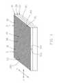
- FIG. 1is a perspective view of the first exemplary embodiment of a conductive plate of the present disclosure.
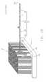
- FIGS. 2A and 2Bare perspective views to illustrate consecutive steps of how a conductive film for the conductive plate of the first exemplary embodiment can be prepared.
- FIG. 2Cis a schematic side view of the conductive film for the conductive plate of the first exemplary embodiment.
- FIG. 2Dis a schematic top view of the conductive film for the conductive plate of the first exemplary embodiment.
- FIG. 3is a perspective view of the second exemplary embodiment of a conductive plate of the present disclosure.
- FIG. 4is a perspective view of the third exemplary embodiment of a conductive plate of the present disclosure.
- the first exemplary embodiment of a conductive plate of the present disclosure for a display panelincludes a substrate 10 and a light-transmissible conductive layer 30 attached to an upper surface 105 of the substrate 10 through an adhesive 20 .
- the conductive layer 30includes a plurality of light-transmissible conductive films 3 , each of which includes a plurality of nanounits 21 .
- the substrate 10can be made of a transparent material, such as glass and a transparent polymeric material.
- the polymeric materialinclude but are not limited to polymethylmethacrylate (PMMA) board, polyethylene terephthalate (PET) board, and polycarbonate (PC) board.
- the substrate 10can also be made of an opaque material, such as metal substrates, semiconductor substrates, printed circuit boards, colored plastic boards, and plastic boards coated with a color layer.
- each of the conductive films 3is made of a nanomaterial and includes strings 31 formed by interconnecting the nanounits 21 (see FIGS. 2A to 2D ).
- the conductive film 3exhibits electric anisotropy (i.e., the conductive film 3 exhibits different resistivities in different directions).
- the nanounits 21 of each of the strings 31are connected in series to one another along a first direction (X) in an end-to-end manner.
- the nanounits 21may be nanotube bundles, nanotubes (anisotropic in shape), or nanoparticles (isotropic in shape).
- the interconnected nanounits 21are carbon nanotube bundles.
- the strings 31 of the nanounits 21extend along the first direction (X) (see FIG.
- the conductive film 3has a much higher conductivity or a much lower resistivity in the first direction (X) than that in the second direction (Y). As illustrated in FIGS.
- the conductive film 3is prepared by forming a cluster 2 of the nanounits 21 on a supporting substrate 4 through chemical vapor deposition techniques, laser vaporization vapor deposition techniques, arc discharge vaporization vapor deposition techniques, followed by removing the nanounits 21 in a pulling manner from the supporting substrate 4 to make them interconnected to form the strings 31 of the nanounits 21 and subsequently stretching the strings 31 of the nanounits 21 along the first direction (X) to form each conductive film 3 .
- the nanounits 21 of each string 31 of each conductive film 3are interconnected through Van der Waals' interaction.
- the adhesive 20depends on the type of curing to be used in bonding the conductive layer 30 to the substrate 10 .
- the adhesive 200is a light curable adhesive (such as an ultraviolet glue)
- the adhesive 200is cured by irradiation with a light having a specified wavelength range
- the adhesive 200is a heat curable adhesive
- the adhesive 200is cured over an elevated temperature
- the adhesive 200is a light-heat curable adhesive
- the adhesive 200is cured by irradiation with the light having a specified wavelength range over an elevated temperature.
- the adhesive 20can also be selected from conductive adhesives, such as a conductive polymer adhesive.
- each of the conductive films 3is adhesively bonded to the upper surface 105 of the substrate 10 through the adhesive 20 .
- the adhesive 20can be applied to the upper surface 105 of the substrate 10 through spin coating, screen printing or liquid drop coating techniques.
- Each of the conductive films 3has first and second end portions 35 , 36 that are opposite to each other in a film-extension direction (U).
- Each of the first and second end portions 35 , 36has an end face 351 , 361 .
- the conductive films 3are arranged on the substrate 10 in a such manner that the strings 31 of all the conductive films 3 substantially extend along the first direction (X) which is different from the film-extension direction (U) (for instance, the first direction (X) and the film-extension direction (U) are transverse to each other) and that the conductive films 3 are distributed along the film-extension direction (U) and are connected in series to one another in an end-to-end manner. That is, the end face 351 of the first end portion 35 of each of the conductive films 3 is connected to the end face 361 of the second end portion 36 of an adjacent one of the conductive films 3 , thereby permitting the conductive film 3 to have a large area and facilitating manufacture of a large size display panel.
- Each of the conductive films 3can be patterned through laser techniques so as to remove an undesired portion of the conductive film 3 and so as to improve the light transmissibility and/or the electric anisotropy (the surface resistivity ratio of the first direction (X) to the second direction (Y)) of the conductive film 3 before the conductive film 3 is attached to the substrate 10 .
- the patterningcan be conducted by moving a laser beam (not shown) above the conductive film 3 along either the first direction (X) or the second direction (Y) or along a predetermined path.
- FIG. 3illustrates the second exemplary embodiment of a conductive plate of the present disclosure.
- the conductive plate of the second exemplary embodimentdiffers from the previous exemplary embodiment in that the conductive films 3 are arranged on the substrate 10 in such a manner that the first end portion 35 of each of the conductive films 3 is stacked on and is attached to the second end portion 36 of an adjacent one of the conductive films 3 .
- the arrangement of the conductive films 3 in this exemplary embodimentaims to overcome a potential problem of the first exemplary embodiment that the connection between the end face 351 of the first end portion 35 of each of the conductive films 3 and the end face 361 of the second end portion 36 of an adjacent one of the conductive films 3 is likely to be ruined due to undesired shrinking of the conductive films 3 (note that each conductive film 3 is formed through a stretching process).
- the stacking of the first and second end portions 35 , 36can result in a decrease in the light transmissibility at the overlapping area.
- first and second end portions 35 , 36 of each of the conductive films 3is removed than that of the remainder of the conductive film 3 through the laser treatment so as to alleviate the adverse effect on the light transmissibility at the stacked first and second end portions 35 , 36 .
- FIG. 4illustrates the third exemplary embodiment of a conductive plate of the present disclosure.
- the conductive plate of the third exemplary embodimentdiffers from the previous exemplary embodiments in that the conductive films 3 are adhesively stacked one another to form into a stack that defines the conductive layer 30 .
- the stackis attached to the surface 105 of the substrate 10 through the adhesive 20 .
- the conductive films 3may also be attached to one another through the adhesive 20 .
- the strings 31 of all the conductive films 3substantially extend along the same direction (X). The surface resistivity of the conductive layer 30 thus formed can be reduced, thereby increasing the maximum transmission current value of the conductive layer 30 .
Landscapes
- Engineering & Computer Science (AREA)
- Microelectronics & Electronic Packaging (AREA)
- Laminated Bodies (AREA)
- Devices For Indicating Variable Information By Combining Individual Elements (AREA)
- Non-Insulated Conductors (AREA)
Abstract
Description
Claims (5)
Applications Claiming Priority (2)
| Application Number | Priority Date | Filing Date | Title |
|---|---|---|---|
| CN2009103050938ACN101989469A (en) | 2009-07-31 | 2009-07-31 | Current-conducting plate |
| CN200910305093.8 | 2009-07-31 |
Publications (2)
| Publication Number | Publication Date |
|---|---|
| US20110024166A1 US20110024166A1 (en) | 2011-02-03 |
| US8487193B2true US8487193B2 (en) | 2013-07-16 |
Family
ID=43525928
Family Applications (1)
| Application Number | Title | Priority Date | Filing Date |
|---|---|---|---|
| US12/826,710Expired - Fee RelatedUS8487193B2 (en) | 2009-07-31 | 2010-06-30 | Conductive plate |
Country Status (2)
| Country | Link |
|---|---|
| US (1) | US8487193B2 (en) |
| CN (1) | CN101989469A (en) |
Families Citing this family (14)
| Publication number | Priority date | Publication date | Assignee | Title |
|---|---|---|---|---|
| US10543662B2 (en) | 2012-02-08 | 2020-01-28 | Corning Incorporated | Device modified substrate article and methods for making |
| US9340443B2 (en) | 2012-12-13 | 2016-05-17 | Corning Incorporated | Bulk annealing of glass sheets |
| TWI617437B (en) | 2012-12-13 | 2018-03-11 | 康寧公司 | Facilitated processing for controlling bonding between sheet and carrier |
| US10014177B2 (en) | 2012-12-13 | 2018-07-03 | Corning Incorporated | Methods for processing electronic devices |
| US10086584B2 (en) | 2012-12-13 | 2018-10-02 | Corning Incorporated | Glass articles and methods for controlled bonding of glass sheets with carriers |
| US10510576B2 (en) | 2013-10-14 | 2019-12-17 | Corning Incorporated | Carrier-bonding methods and articles for semiconductor and interposer processing |
| CN106132688B (en) | 2014-01-27 | 2020-07-14 | 康宁股份有限公司 | Article and method for controlled bonding of a sheet to a carrier |
| EP3129221A1 (en) | 2014-04-09 | 2017-02-15 | Corning Incorporated | Device modified substrate article and methods for making |
| EP3297824A1 (en) | 2015-05-19 | 2018-03-28 | Corning Incorporated | Articles and methods for bonding sheets with carriers |
| KR102524620B1 (en) | 2015-06-26 | 2023-04-21 | 코닝 인코포레이티드 | Methods and articles including sheets and carriers |
| TW201825623A (en) | 2016-08-30 | 2018-07-16 | 美商康寧公司 | Peptide plasma polymer for sheet bonding |
| TWI821867B (en) | 2016-08-31 | 2023-11-11 | 美商康寧公司 | Articles of controllably bonded sheets and methods for making same |
| JP7260523B2 (en) | 2017-08-18 | 2023-04-18 | コーニング インコーポレイテッド | Temporary binding using polycationic polymers |
| US11331692B2 (en) | 2017-12-15 | 2022-05-17 | Corning Incorporated | Methods for treating a substrate and method for making articles comprising bonded sheets |
Citations (9)
| Publication number | Priority date | Publication date | Assignee | Title |
|---|---|---|---|---|
| US20040047038A1 (en)* | 2002-09-10 | 2004-03-11 | Kai-Li Jiang | Optical polarizer and method for fabricating such optical polarizer |
| US20040051432A1 (en)* | 2002-09-16 | 2004-03-18 | Jiang Kaili | Light filament formed from carbon nanotubes and method for making same |
| US20040053780A1 (en)* | 2002-09-16 | 2004-03-18 | Jiang Kaili | Method for fabricating carbon nanotube yarn |
| US20050209392A1 (en) | 2003-12-17 | 2005-09-22 | Jiazhong Luo | Polymer binders for flexible and transparent conductive coatings containing carbon nanotubes |
| WO2007015710A2 (en) | 2004-11-09 | 2007-02-08 | Board Of Regents, The University Of Texas System | The fabrication and application of nanofiber ribbons and sheets and twisted and non-twisted nanofiber yarns |
| US20070296897A1 (en)* | 2006-06-23 | 2007-12-27 | Tsinghua University | Liquid crystal cell assembly for liquid crystal display |
| US20080245548A1 (en)* | 2007-04-06 | 2008-10-09 | Tsinghua University | Conductive tape and method for making the same |
| US20090101488A1 (en)* | 2007-10-23 | 2009-04-23 | Tsinghua University | Touch panel |
| US20100233472A1 (en)* | 2008-02-01 | 2010-09-16 | Tsinghua University | Carbon nanotube composite film |
- 2009
- 2009-07-31CNCN2009103050938Apatent/CN101989469A/enactivePending
- 2010
- 2010-06-30USUS12/826,710patent/US8487193B2/ennot_activeExpired - Fee Related
Patent Citations (10)
| Publication number | Priority date | Publication date | Assignee | Title |
|---|---|---|---|---|
| US20040047038A1 (en)* | 2002-09-10 | 2004-03-11 | Kai-Li Jiang | Optical polarizer and method for fabricating such optical polarizer |
| US20040051432A1 (en)* | 2002-09-16 | 2004-03-18 | Jiang Kaili | Light filament formed from carbon nanotubes and method for making same |
| US20040053780A1 (en)* | 2002-09-16 | 2004-03-18 | Jiang Kaili | Method for fabricating carbon nanotube yarn |
| US20050209392A1 (en) | 2003-12-17 | 2005-09-22 | Jiazhong Luo | Polymer binders for flexible and transparent conductive coatings containing carbon nanotubes |
| WO2007015710A2 (en) | 2004-11-09 | 2007-02-08 | Board Of Regents, The University Of Texas System | The fabrication and application of nanofiber ribbons and sheets and twisted and non-twisted nanofiber yarns |
| US20070296897A1 (en)* | 2006-06-23 | 2007-12-27 | Tsinghua University | Liquid crystal cell assembly for liquid crystal display |
| US20080245548A1 (en)* | 2007-04-06 | 2008-10-09 | Tsinghua University | Conductive tape and method for making the same |
| US20090101488A1 (en)* | 2007-10-23 | 2009-04-23 | Tsinghua University | Touch panel |
| US20100233472A1 (en)* | 2008-02-01 | 2010-09-16 | Tsinghua University | Carbon nanotube composite film |
| US8012585B2 (en)* | 2008-02-01 | 2011-09-06 | Tsinghua University | Carbon nanotube composite film |
Also Published As
| Publication number | Publication date |
|---|---|
| CN101989469A (en) | 2011-03-23 |
| US20110024166A1 (en) | 2011-02-03 |
Similar Documents
| Publication | Publication Date | Title |
|---|---|---|
| US8487193B2 (en) | Conductive plate | |
| US10643503B2 (en) | Motherboard and manufacturing method thereof, cover plate and manufacturing method thereof, and display device | |
| US8623224B2 (en) | Method for making patterned conductive element | |
| US20130092426A1 (en) | Anisotropic conductive film and fabrication method thereof | |
| US20110005815A1 (en) | Conductive plate and touch panel including the same | |
| TW201737440A (en) | Touch panel and junction structure of touch panel and flexible printed circuit board | |
| US10932364B2 (en) | Transparent conductive film | |
| JP2013122745A (en) | Touch panel and manufacturing method thereof | |
| CN103971788B (en) | Transparent conductive body and preparation method thereof | |
| US20170285780A1 (en) | Touch sensor and method for preparing the same | |
| CN111295723B (en) | Embedded transparent electrode substrate and its manufacturing method | |
| KR20200021425A (en) | Embedded electrode substrate for transparent light emitting device display and method for manufacturing thereof | |
| CN103559944A (en) | Foldable Conductive Films and Displays | |
| US9075489B2 (en) | Method for making touch panel | |
| KR101555080B1 (en) | Touch sensor intergrated with a polarizer and display device comprising the same | |
| US8454787B2 (en) | Method for making patterned conductive element | |
| US20140024155A1 (en) | Method for making liquid crystal display module | |
| US20110005819A1 (en) | Conductive plate and method for making the same | |
| CN104238855B (en) | Touching display screen | |
| US20150060251A1 (en) | Touch panel and method for making the same | |
| JP2003231202A (en) | Barrier film and conductive barrier film | |
| US20150059970A1 (en) | Method for making touch panel | |
| US20140024280A1 (en) | Method for making liquid crystal display module | |
| JP2014232375A (en) | Sensor sheet and method for manufacturing the same | |
| US20150059971A1 (en) | Method for making touch panel |
Legal Events
| Date | Code | Title | Description |
|---|---|---|---|
| AS | Assignment | Owner name:CHIMEI INNOLUX CORPORATION, TAIWAN Free format text:ASSIGNMENT OF ASSIGNORS INTEREST;ASSIGNORS:CHANG, CHIH-CHIEH;WU, JEAH-SHENG;CHAO, CHIH-HAN;REEL/FRAME:024613/0940 Effective date:20100628 | |
| STCF | Information on status: patent grant | Free format text:PATENTED CASE | |
| AS | Assignment | Owner name:INNOLUX CORPORATION, TAIWAN Free format text:CHANGE OF NAME;ASSIGNOR:CHIMEI INNOLUX CORPORATION;REEL/FRAME:032672/0813 Effective date:20121219 | |
| FPAY | Fee payment | Year of fee payment:4 | |
| MAFP | Maintenance fee payment | Free format text:PAYMENT OF MAINTENANCE FEE, 8TH YEAR, LARGE ENTITY (ORIGINAL EVENT CODE: M1552); ENTITY STATUS OF PATENT OWNER: LARGE ENTITY Year of fee payment:8 | |
| FEPP | Fee payment procedure | Free format text:MAINTENANCE FEE REMINDER MAILED (ORIGINAL EVENT CODE: REM.); ENTITY STATUS OF PATENT OWNER: LARGE ENTITY | |
| LAPS | Lapse for failure to pay maintenance fees | Free format text:PATENT EXPIRED FOR FAILURE TO PAY MAINTENANCE FEES (ORIGINAL EVENT CODE: EXP.); ENTITY STATUS OF PATENT OWNER: LARGE ENTITY | |
| STCH | Information on status: patent discontinuation | Free format text:PATENT EXPIRED DUE TO NONPAYMENT OF MAINTENANCE FEES UNDER 37 CFR 1.362 | |
| FP | Lapsed due to failure to pay maintenance fee | Effective date:20250716 |