US8486285B2 - Damascene write poles produced via full film plating - Google Patents
Damascene write poles produced via full film platingDownload PDFInfo
- Publication number
- US8486285B2 US8486285B2US12/544,998US54499809AUS8486285B2US 8486285 B2US8486285 B2US 8486285B2US 54499809 AUS54499809 AUS 54499809AUS 8486285 B2US8486285 B2US 8486285B2
- Authority
- US
- United States
- Prior art keywords
- layer
- over
- wafer
- magnetic material
- forming
- Prior art date
- Legal status (The legal status is an assumption and is not a legal conclusion. Google has not performed a legal analysis and makes no representation as to the accuracy of the status listed.)
- Expired - Fee Related, expires
Links
- 238000007747platingMethods0.000titleclaimsabstractdescription14
- 239000000696magnetic materialSubstances0.000claimsabstractdescription54
- 238000000034methodMethods0.000claimsabstractdescription49
- 239000000463materialSubstances0.000claimsabstractdescription47
- 239000000758substrateSubstances0.000claimsabstractdescription32
- 238000003801millingMethods0.000claimsabstractdescription23
- 238000005530etchingMethods0.000claimsabstractdescription21
- 238000005498polishingMethods0.000claimsabstractdescription12
- 229920002120photoresistant polymerPolymers0.000claimsdescription13
- PNEYBMLMFCGWSK-UHFFFAOYSA-Naluminium oxideInorganic materials[O-2].[O-2].[O-2].[Al+3].[Al+3]PNEYBMLMFCGWSK-UHFFFAOYSA-N0.000claimsdescription12
- 229910017107AlOxInorganic materials0.000claimsdescription4
- 238000010884ion-beam techniqueMethods0.000claimsdescription4
- OKTJSMMVPCPJKN-UHFFFAOYSA-NCarbonChemical compound[C]OKTJSMMVPCPJKN-UHFFFAOYSA-N0.000claimsdescription2
- 229910003321CoFeInorganic materials0.000claimsdescription2
- 229910001030Iron–nickel alloyInorganic materials0.000claimsdescription2
- 229910052799carbonInorganic materials0.000claimsdescription2
- 239000000126substanceSubstances0.000claimsdescription2
- 238000004519manufacturing processMethods0.000description6
- 238000001020plasma etchingMethods0.000description5
- 238000000231atomic layer depositionMethods0.000description4
- 230000015572biosynthetic processEffects0.000description4
- 239000011651chromiumSubstances0.000description4
- 238000001000micrographMethods0.000description4
- 229910052593corundumInorganic materials0.000description3
- 238000007373indentationMethods0.000description3
- 229910001845yogo sapphireInorganic materials0.000description3
- VYZAMTAEIAYCRO-UHFFFAOYSA-NChromiumChemical compound[Cr]VYZAMTAEIAYCRO-UHFFFAOYSA-N0.000description2
- 229910052804chromiumInorganic materials0.000description2
- 238000012986modificationMethods0.000description2
- 230000004048modificationEffects0.000description2
- 229910052715tantalumInorganic materials0.000description2
- GUVRBAGPIYLISA-UHFFFAOYSA-Ntantalum atomChemical compound[Ta]GUVRBAGPIYLISA-UHFFFAOYSA-N0.000description2
- KJTLSVCANCCWHF-UHFFFAOYSA-NRutheniumChemical compound[Ru]KJTLSVCANCCWHF-UHFFFAOYSA-N0.000description1
- 239000000654additiveSubstances0.000description1
- 230000000996additive effectEffects0.000description1
- 230000001939inductive effectEffects0.000description1
- 230000002829reductive effectEffects0.000description1
- 229910052707rutheniumInorganic materials0.000description1
Images


Classifications
- G—PHYSICS
- G11—INFORMATION STORAGE
- G11B—INFORMATION STORAGE BASED ON RELATIVE MOVEMENT BETWEEN RECORD CARRIER AND TRANSDUCER
- G11B5/00—Recording by magnetisation or demagnetisation of a record carrier; Reproducing by magnetic means; Record carriers therefor
- G11B5/84—Processes or apparatus specially adapted for manufacturing record carriers
- G11B5/855—Coating only part of a support with a magnetic layer
- Y—GENERAL TAGGING OF NEW TECHNOLOGICAL DEVELOPMENTS; GENERAL TAGGING OF CROSS-SECTIONAL TECHNOLOGIES SPANNING OVER SEVERAL SECTIONS OF THE IPC; TECHNICAL SUBJECTS COVERED BY FORMER USPC CROSS-REFERENCE ART COLLECTIONS [XRACs] AND DIGESTS
- Y10—TECHNICAL SUBJECTS COVERED BY FORMER USPC
- Y10T—TECHNICAL SUBJECTS COVERED BY FORMER US CLASSIFICATION
- Y10T29/00—Metal working
- Y10T29/49—Method of mechanical manufacture
- Y10T29/49002—Electrical device making
- Y10T29/4902—Electromagnet, transformer or inductor
- Y10T29/49021—Magnetic recording reproducing transducer [e.g., tape head, core, etc.]
- Y10T29/49032—Fabricating head structure or component thereof
- Y10T29/49048—Machining magnetic material [e.g., grinding, etching, polishing]
Definitions
- the present inventiongenerally relates to hard disk drives and, in particular, relates to producing damascene write poles via full film plating.
- Hard disk drivesinclude one or more rigid disks, which are coated with a magnetic recording medium in which data can be stored. Hard disk drives further include read and write heads for interacting with the data in the magnetic recording medium.
- the write headincludes an inductive element for generating a magnetic field that aligns the magnetic moments of domains in the magnetic recording medium to represent bits of data.
- Magnetic recording techniquesinclude both longitudinal and perpendicular recording.
- Perpendicular magnetic recording (“PMR”)is a form of magnetic recording in which the magnetic moments representing bits of data are oriented perpendicularly to the surface of the magnetic recording medium, as opposed to longitudinally along a track thereof. PMR enjoys a number of advantages over longitudinal recording, such as significantly higher areal density recording capability.
- Write poles with a trapezoidal cross-sectional shape at the air bearing surface (“ABS”)are used to provide improved writing performance in PMR heads.
- ABSair bearing surface
- the manufacture of write poles with this trapezoidal cross-sectional shapepresents a number of difficulties, however.
- One approach to manufacturing such polesinvolves a reductive process of milling poles from a layer of magnetic material. Due to the complex three-dimensional shapes called for in next-generation hard disk drives, however, this process can be extraordinarily difficult and prone to low yields.
- Another approach to manufacturing these polesinvolves an additive process, in which damascene trenches are formed in an insulating substrate layer and filled with a magnetic material.
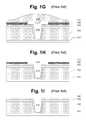
- FIGS. 1A-1IOne such approach to forming a write pole is illustrated in FIGS. 1A-1I .
- a patterned mask 103 of tantalum (Ta)is provided over a substrate 102 of alumina (Al 2 O 3 ) disposed on a lower substrate 101 of chromium (Cr).
- Patterned mask 103has an opening 104 over a region of substrate 102 where a damascene trench will be formed.
- RIEreactive ion etching
- one or more layers of aluminamay be disposed via atomic layer deposition (ALD) over the structure of FIG. 1B to provide a narrower damascene trench 107 , as is illustrated in FIG. 1C .
- ALDatomic layer deposition
- a layer of photoresist 108is applied over the structure of FIG. 1C to open an area 109 over damascene trench 107 .
- a high moment magnetic material 110such as CoNiFe or the like, is then plated to fill the trench pattern formed by the foregoing photoresist process, as is illustrated in FIG. 1E .
- the photoresistis then stripped from the structure to create an open area on the field surrounding magnetic material 110 , and a stop layer 111 , such as diamond-like carbon (DLC), is deposited over the field area, as is illustrated in FIG. 1F .
- the stop layerallows a chemical mechanical polishing (CMP) operation to be used to remove excess magnetic material extending above the desired trailing edge of the write pole, as will be illustrated in greater detail below.
- CMPchemical mechanical polishing
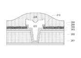
- FIG. 1Fanother layer 112 of Al 2 O 3 is provided over the structure of FIG. 1F , as is illustrated in FIG. 1G .
- the structureis subjected to the CMP process to planarize the surface on the top of stop layer 111 , as is illustrated in FIG. 1H .
- the thickness and track width of write pole 113are well preserved by stopping the CMP process within the thickness of stop layer 111 , but where the stop layer has a gap 114 surrounding write pole 113 , however, dishing in the trailing edge of write pole 113 may occur.
- the remaining material from stop layer 111is removed by another RIE process, as is illustrated in FIG. 1I .
- the use of photoresist to define a frame for plating the magnetic materialmay leave undesirable photoresist residue within the damascene trench and along the side walls of the write poles thus formed. Any photoresist residue can result in poor pole integrity and finishing, and may even result in device failure.
- Various embodiments of the present inventionsolve the foregoing problems by providing methods for forming write poles that use a full-film plating of magnetic material to avoid surrounding a write pole with photoresist residue. Moreover, a full-film ion beam etch is used to remove excess magnetic material from the field area after full-film plating, greatly simplifying the pole formation process. A sacrificial buffer layer is provided between the full-film plated magnetic material and a CMP stop layer, such that the ion beam etching or milling used to remove the excess magnetic material does not reach the CMP stop layer and impact its effectiveness.
- a method for forming a write polecomprises the step of forming a stop layer over a substrate layer of a wafer, the stop layer having an opening above a damascene trench in the substrate layer.
- the methodfurther comprises the step of forming a buffer layer over the stop layer, the buffer layer having an opening above the opening of the stop layer.
- the methodfurther comprises the steps of plating a layer of magnetic material over the wafer, disposing a first sacrificial material over a region of the magnetic material above the damascene trench, and performing a etching or milling operation over the wafer to remove the magnetic material not covered by the first sacrificial material and to remove the first sacrificial material.
- the methodfurther comprises the steps of disposing a second sacrificial material over the wafer, and performing a polishing operation over the wafer to remove the region of the magnetic material above the damascene trench, to remove the second sacrificial material, and to remove the buffer layer.
- a method for forming a plurality of write polescomprises the step of forming a stop layer over a substrate layer of a wafer, the stop layer having a first plurality of openings above a corresponding plurality of damascene trenches in the substrate layer.
- the methodfurther comprises the step of forming a buffer layer over the stop layer, the buffer layer having a second plurality of openings above corresponding ones of the first plurality of openings of the stop layer.
- the methodfurther comprises the steps of plating a layer of magnetic material over the wafer, disposing a first sacrificial material over a plurality of regions of the magnetic material above corresponding ones of the plurality of damascene trenches, and performing a milling or etching operation over the wafer to remove the magnetic material not covered by the first sacrificial material and to remove the first sacrificial material.
- the methodfurther comprises the steps of disposing a second sacrificial material over the wafer and performing a polishing operation over the wafer to remove the plurality of regions of the magnetic material above the corresponding ones of the plurality of damascene trenches, to remove the second sacrificial material, and to remove the buffer layer.
- FIGS. 1A-1Iillustrate structures formed after various steps in the formation of a write pole
- FIGS. 2A-2Iillustrate structures formed after various steps in the formation of a write pole in accordance with one aspect of the subject disclosure
- FIG. 3is a scanning electron microscope image of a partially-formed write pole after excess magnetic material has been removed by a milling or etching operation in accordance with one aspect of the subject disclosure
- FIG. 4is a scanning electron microscope image of a write pole formed in accordance with one aspect of the subject disclosure
- FIG. 5is a flow chart illustrating a method for forming a write pole in accordance with one aspect of the subject disclosure.
- FIG. 6is a flow chart illustrating a method for forming a plurality of write poles in accordance with one aspect of the subject disclosure.
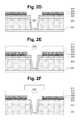
- FIGS. 2A-2Iillustrate structures formed after various steps in the formation of a write pole in accordance with one aspect of the subject disclosure.
- a patterned mask 203 of tantalum (Ta) or the likeis provided over a substrate 202 of alumina (Al 2 O 3 ) disposed on a lower substrate 201 of chromium (Cr) or the like.
- Patterned mask 203has an opening 204 over a region of substrate 202 where a damascene trench will be formed.
- RIEreactive ion etching
- one or more layers of aluminamay be disposed via atomic layer deposition (ALD) over the structure of FIG. 2B to provide a narrower damascene trench 207 , as is illustrated in FIG. 2C .
- ALDatomic layer deposition
- a CMP stop layer 208 of DLC or the likeis provided over layer 206 .
- the material of CMP stop layer 208may be selected such that a CMP selectivity (i.e., a relative rate of material removal) between the magnetic material and the stop layer material is greater than 300:1.
- a sacrificial buffer layer 209 of AlO x(where x is a positive integer) is provided over CMP stop layer 208 to protect CMP stop layer 208 from a subsequent milling or etching operation, as is set forth in greater detail below.
- a seed layer 210 of ruthenium (Ru) or the likeis provided over the wafer and a layer of high moment magnetic material 211 , of CoNiFe, CoFe, NiFe or the like, is plated over the wafer above seed layer 210 .
- an indentation 212may be formed in the region above damascene trench 207 thus filled by magnetic material.
- This indentation 212may assist in aligning the application of a region of photoresist 213 as illustrated in greater detail with respect to FIG. 2F , below. Moreover, this indentation may allow for a subsequent CMP operation to more quickly remove the excess magnetic material from above the desired trailing edge of the write pole than would be possible if the excess material had a planar upper surface.
- photoresist 213serves as a mask to protect the region of magnetic material 211 covered thereby, such that a subsequent ion beam etching (IBE) or milling operation will not remove the magnetic material from the region immediately surrounding (and filling) the damascene trench. This is illustrated in greater detail with respect to FIG. 2G , in which the post-milling structure is illustrated.
- the full-film IBE or milling operationremoves most of photoresist material 213 , the excess magnetic material and the seed layer material surrounding the pole region, but removes only part of the sacrificial buffer layer 209 of AlO x .
- Buffer layer 209has thereby served its purpose of protecting CMP stop layer 208 from being damaged by the milling or etching operation, ensuring that CMP stop layer will be able to provide a readily-detectable end-point for a subsequent CMP operation, as is set forth in greater detail below.
- the small protrusion of magnetic material 211 left after the etching or milling operationallow for shorter polishing times and higher planarization efficiency. Any residue from photoresist material 213 not removed by the full-film IBE or milling operation may be removed via lift-off at this time.
- FIG. 3a scanning electron microscope image of a partially-formed write pole is illustrated in cross-section after the excess magnetic material has been removed by a milling or etching operation in accordance with one aspect of the subject disclosure.
- a portion of the AlO x bufferremains intact, protecting the CMP stop layer of DLC from the etching or milling operation.
- a sacrificial layer 214 of alumina or the likeis disposed over the wafer, covering magnetic material 211 and providing a more uniform surface for a CMP operation.
- the CMP operationis performed, removing this sacrificial layer 214 , the remaining buffer layer 209 , and the excess magnetic material to form write pole 213 .
- the CMP operationstops when the stop layer 208 is detected (e.g., when the polishing removal rate slows upon encountering the DLC).
- the remaining seed layer 210 of Rumay be used in a subsequent local CMP operation (as opposed to the foregoing global or wafer-wide CMP operation) as a per-write pole stop layer.
- FIG. 4is a scanning electron microscope image of a write pole formed in accordance with one aspect of the subject disclosure. As can be seen with reference to FIG. 4 , the write pole experiences minimal dishing, and is free from the photoresist residue which can contaminate write poles produced with a framed plating approach.
- FIG. 5is a flow chart illustrating a method for forming a write pole in accordance with one aspect of the subject disclosure.
- the methodbegins with step 501 , in which a patterned mask layer is formed over a substrate layer of a wafer.
- step 502a region of the substrate layer exposed by the patterned mask layer is etched to form a damascene trench in the substrate layer.
- step 503a layer of alumina is disposed over the wafer to adjust a width of the damascene trench.
- a stop layeris formed over the substrate, the stop layer having an opening above the damascene trench.
- a buffer layeris formed over the stop layer, the buffer layer having an opening above the opening of the stop layer.
- a seed layeris disposed over the wafer, and in step 507 , a layer of magnetic material is plated over the wafer.
- a first sacrificial materialis disposed over a region of the magnetic material above the damascene trench.
- a milling or etching operationis performed over the wafer to remove the magnetic material not covered by the first sacrificial material and to remove the first sacrificial material.
- step 510a second sacrificial material is disposed over the wafer, and in step 511 , a polishing operation is performed over the wafer to remove the region of the magnetic material above the damascene trench, to remove the second sacrificial material, and to remove the buffer layer.
- FIG. 6is a flow chart illustrating a method for forming a plurality of write poles in accordance with one aspect of the subject disclosure.
- the methodbegins with step 601 , in which a stop layer is formed over a substrate layer of a wafer, the stop layer having a first plurality of openings above a corresponding plurality of damascene trenches in the substrate layer.
- a buffer layeris formed over the stop layer, the buffer layer having a second plurality of openings above corresponding ones of the first plurality of openings of the stop layer.
- a seed layeris disposed over the wafer, and in step 604 , a layer of magnetic material is plated over the wafer.
- a first sacrificial materialis disposed over a plurality of regions of the magnetic material above corresponding ones of the plurality of damascene trenches.
- step 606a milling or etching operation is performed over the wafer to remove the magnetic material not covered by the first sacrificial material and to remove the first sacrificial material.
- step 607a second sacrificial material is disposed over the wafer.
- step 608a polishing operation is performed over the wafer to remove the plurality of regions of the magnetic material above the corresponding ones of the plurality of damascene trenches, to remove the second sacrificial material, and to remove the buffer layer.
Landscapes
- Magnetic Heads (AREA)
Abstract
Description
Claims (18)
Priority Applications (3)
| Application Number | Priority Date | Filing Date | Title |
|---|---|---|---|
| US12/544,998US8486285B2 (en) | 2009-08-20 | 2009-08-20 | Damascene write poles produced via full film plating |
| CN201010260525.0ACN101996641B (en) | 2009-08-20 | 2010-08-20 | A kind ofly form the write method of pole, the method forming multiple write pole and magnetic recording device |
| HK11104369.2AHK1150254B (en) | 2009-08-20 | 2011-05-03 | A method of forming a write pole, method of forming a plurality of write poles, and magnetic recording device |
Applications Claiming Priority (1)
| Application Number | Priority Date | Filing Date | Title |
|---|---|---|---|
| US12/544,998US8486285B2 (en) | 2009-08-20 | 2009-08-20 | Damascene write poles produced via full film plating |
Publications (2)
| Publication Number | Publication Date |
|---|---|
| US20110042349A1 US20110042349A1 (en) | 2011-02-24 |
| US8486285B2true US8486285B2 (en) | 2013-07-16 |
Family
ID=43604479
Family Applications (1)
| Application Number | Title | Priority Date | Filing Date |
|---|---|---|---|
| US12/544,998Expired - Fee RelatedUS8486285B2 (en) | 2009-08-20 | 2009-08-20 | Damascene write poles produced via full film plating |
Country Status (2)
| Country | Link |
|---|---|
| US (1) | US8486285B2 (en) |
| CN (1) | CN101996641B (en) |
Cited By (132)
| Publication number | Priority date | Publication date | Assignee | Title |
|---|---|---|---|---|
| US8830628B1 (en) | 2009-02-23 | 2014-09-09 | Western Digital (Fremont), Llc | Method and system for providing a perpendicular magnetic recording head |
| US8879207B1 (en) | 2011-12-20 | 2014-11-04 | Western Digital (Fremont), Llc | Method for providing a side shield for a magnetic recording transducer using an air bridge |
| US8883017B1 (en) | 2013-03-12 | 2014-11-11 | Western Digital (Fremont), Llc | Method and system for providing a read transducer having seamless interfaces |
| US8917581B1 (en) | 2013-12-18 | 2014-12-23 | Western Digital Technologies, Inc. | Self-anneal process for a near field transducer and chimney in a hard disk drive assembly |
| US8923102B1 (en) | 2013-07-16 | 2014-12-30 | Western Digital (Fremont), Llc | Optical grating coupling for interferometric waveguides in heat assisted magnetic recording heads |
| US8947985B1 (en) | 2013-07-16 | 2015-02-03 | Western Digital (Fremont), Llc | Heat assisted magnetic recording transducers having a recessed pole |
| US8953422B1 (en) | 2014-06-10 | 2015-02-10 | Western Digital (Fremont), Llc | Near field transducer using dielectric waveguide core with fine ridge feature |
| US8958272B1 (en) | 2014-06-10 | 2015-02-17 | Western Digital (Fremont), Llc | Interfering near field transducer for energy assisted magnetic recording |
| US8971160B1 (en) | 2013-12-19 | 2015-03-03 | Western Digital (Fremont), Llc | Near field transducer with high refractive index pin for heat assisted magnetic recording |
| US8970988B1 (en) | 2013-12-31 | 2015-03-03 | Western Digital (Fremont), Llc | Electric gaps and method for making electric gaps for multiple sensor arrays |
| US8976635B1 (en) | 2014-06-10 | 2015-03-10 | Western Digital (Fremont), Llc | Near field transducer driven by a transverse electric waveguide for energy assisted magnetic recording |
| US8982508B1 (en) | 2011-10-31 | 2015-03-17 | Western Digital (Fremont), Llc | Method for providing a side shield for a magnetic recording transducer |
| US8980109B1 (en) | 2012-12-11 | 2015-03-17 | Western Digital (Fremont), Llc | Method for providing a magnetic recording transducer using a combined main pole and side shield CMP for a wraparound shield scheme |
| US8988825B1 (en) | 2014-02-28 | 2015-03-24 | Western Digital (Fremont, LLC | Method for fabricating a magnetic writer having half-side shields |
| US8988812B1 (en) | 2013-11-27 | 2015-03-24 | Western Digital (Fremont), Llc | Multi-sensor array configuration for a two-dimensional magnetic recording (TDMR) operation |
| US8984740B1 (en) | 2012-11-30 | 2015-03-24 | Western Digital (Fremont), Llc | Process for providing a magnetic recording transducer having a smooth magnetic seed layer |
| US8993217B1 (en) | 2013-04-04 | 2015-03-31 | Western Digital (Fremont), Llc | Double exposure technique for high resolution disk imaging |
| US8995087B1 (en) | 2006-11-29 | 2015-03-31 | Western Digital (Fremont), Llc | Perpendicular magnetic recording write head having a wrap around shield |
| US8997832B1 (en) | 2010-11-23 | 2015-04-07 | Western Digital (Fremont), Llc | Method of fabricating micrometer scale components |
| US9001628B1 (en) | 2013-12-16 | 2015-04-07 | Western Digital (Fremont), Llc | Assistant waveguides for evaluating main waveguide coupling efficiency and diode laser alignment tolerances for hard disk |
| US9001467B1 (en) | 2014-03-05 | 2015-04-07 | Western Digital (Fremont), Llc | Method for fabricating side shields in a magnetic writer |
| US9007879B1 (en) | 2014-06-10 | 2015-04-14 | Western Digital (Fremont), Llc | Interfering near field transducer having a wide metal bar feature for energy assisted magnetic recording |
| US9007719B1 (en) | 2013-10-23 | 2015-04-14 | Western Digital (Fremont), Llc | Systems and methods for using double mask techniques to achieve very small features |
| US9007725B1 (en) | 2014-10-07 | 2015-04-14 | Western Digital (Fremont), Llc | Sensor with positive coupling between dual ferromagnetic free layer laminates |
| US9013836B1 (en) | 2013-04-02 | 2015-04-21 | Western Digital (Fremont), Llc | Method and system for providing an antiferromagnetically coupled return pole |
| US9042051B2 (en) | 2013-08-15 | 2015-05-26 | Western Digital (Fremont), Llc | Gradient write gap for perpendicular magnetic recording writer |
| US9042058B1 (en) | 2013-10-17 | 2015-05-26 | Western Digital Technologies, Inc. | Shield designed for middle shields in a multiple sensor array |
| US9042208B1 (en) | 2013-03-11 | 2015-05-26 | Western Digital Technologies, Inc. | Disk drive measuring fly height by applying a bias voltage to an electrically insulated write component of a head |
| US9042057B1 (en) | 2013-01-09 | 2015-05-26 | Western Digital (Fremont), Llc | Methods for providing magnetic storage elements with high magneto-resistance using Heusler alloys |
| US9042052B1 (en) | 2014-06-23 | 2015-05-26 | Western Digital (Fremont), Llc | Magnetic writer having a partially shunted coil |
| US9053735B1 (en) | 2014-06-20 | 2015-06-09 | Western Digital (Fremont), Llc | Method for fabricating a magnetic writer using a full-film metal planarization |
| US9064527B1 (en) | 2013-04-12 | 2015-06-23 | Western Digital (Fremont), Llc | High order tapered waveguide for use in a heat assisted magnetic recording head |
| US9065043B1 (en) | 2012-06-29 | 2015-06-23 | Western Digital (Fremont), Llc | Tunnel magnetoresistance read head with narrow shield-to-shield spacing |
| US9064528B1 (en) | 2013-05-17 | 2015-06-23 | Western Digital Technologies, Inc. | Interferometric waveguide usable in shingled heat assisted magnetic recording in the absence of a near-field transducer |
| US9064507B1 (en) | 2009-07-31 | 2015-06-23 | Western Digital (Fremont), Llc | Magnetic etch-stop layer for magnetoresistive read heads |
| US9070381B1 (en) | 2013-04-12 | 2015-06-30 | Western Digital (Fremont), Llc | Magnetic recording read transducer having a laminated free layer |
| US9082423B1 (en) | 2013-12-18 | 2015-07-14 | Western Digital (Fremont), Llc | Magnetic recording write transducer having an improved trailing surface profile |
| US9087527B1 (en) | 2014-10-28 | 2015-07-21 | Western Digital (Fremont), Llc | Apparatus and method for middle shield connection in magnetic recording transducers |
| US9087534B1 (en) | 2011-12-20 | 2015-07-21 | Western Digital (Fremont), Llc | Method and system for providing a read transducer having soft and hard magnetic bias structures |
| US9093639B2 (en) | 2012-02-21 | 2015-07-28 | Western Digital (Fremont), Llc | Methods for manufacturing a magnetoresistive structure utilizing heating and cooling |
| US9104107B1 (en) | 2013-04-03 | 2015-08-11 | Western Digital (Fremont), Llc | DUV photoresist process |
| US9111558B1 (en) | 2014-03-14 | 2015-08-18 | Western Digital (Fremont), Llc | System and method of diffractive focusing of light in a waveguide |
| US9111550B1 (en) | 2014-12-04 | 2015-08-18 | Western Digital (Fremont), Llc | Write transducer having a magnetic buffer layer spaced between a side shield and a write pole by non-magnetic layers |
| US9111564B1 (en) | 2013-04-02 | 2015-08-18 | Western Digital (Fremont), Llc | Magnetic recording writer having a main pole with multiple flare angles |
| US9123358B1 (en) | 2012-06-11 | 2015-09-01 | Western Digital (Fremont), Llc | Conformal high moment side shield seed layer for perpendicular magnetic recording writer |
| US9123374B1 (en) | 2015-02-12 | 2015-09-01 | Western Digital (Fremont), Llc | Heat assisted magnetic recording writer having an integrated polarization rotation plate |
| US9123359B1 (en) | 2010-12-22 | 2015-09-01 | Western Digital (Fremont), Llc | Magnetic recording transducer with sputtered antiferromagnetic coupling trilayer between plated ferromagnetic shields and method of fabrication |
| US9123362B1 (en) | 2011-03-22 | 2015-09-01 | Western Digital (Fremont), Llc | Methods for assembling an electrically assisted magnetic recording (EAMR) head |
| US9135937B1 (en) | 2014-05-09 | 2015-09-15 | Western Digital (Fremont), Llc | Current modulation on laser diode for energy assisted magnetic recording transducer |
| US9135930B1 (en) | 2014-03-06 | 2015-09-15 | Western Digital (Fremont), Llc | Method for fabricating a magnetic write pole using vacuum deposition |
| US9142233B1 (en) | 2014-02-28 | 2015-09-22 | Western Digital (Fremont), Llc | Heat assisted magnetic recording writer having a recessed pole |
| US9147408B1 (en) | 2013-12-19 | 2015-09-29 | Western Digital (Fremont), Llc | Heated AFM layer deposition and cooling process for TMR magnetic recording sensor with high pinning field |
| US9147404B1 (en) | 2015-03-31 | 2015-09-29 | Western Digital (Fremont), Llc | Method and system for providing a read transducer having a dual free layer |
| US9153255B1 (en) | 2014-03-05 | 2015-10-06 | Western Digital (Fremont), Llc | Method for fabricating a magnetic writer having an asymmetric gap and shields |
| US9183854B2 (en) | 2014-02-24 | 2015-11-10 | Western Digital (Fremont), Llc | Method to make interferometric taper waveguide for HAMR light delivery |
| US9190085B1 (en) | 2014-03-12 | 2015-11-17 | Western Digital (Fremont), Llc | Waveguide with reflective grating for localized energy intensity |
| US9190079B1 (en) | 2014-09-22 | 2015-11-17 | Western Digital (Fremont), Llc | Magnetic write pole having engineered radius of curvature and chisel angle profiles |
| US9194692B1 (en) | 2013-12-06 | 2015-11-24 | Western Digital (Fremont), Llc | Systems and methods for using white light interferometry to measure undercut of a bi-layer structure |
| US9202480B2 (en) | 2009-10-14 | 2015-12-01 | Western Digital (Fremont), LLC. | Double patterning hard mask for damascene perpendicular magnetic recording (PMR) writer |
| US9202493B1 (en) | 2014-02-28 | 2015-12-01 | Western Digital (Fremont), Llc | Method of making an ultra-sharp tip mode converter for a HAMR head |
| US9213322B1 (en) | 2012-08-16 | 2015-12-15 | Western Digital (Fremont), Llc | Methods for providing run to run process control using a dynamic tuner |
| US9214172B2 (en) | 2013-10-23 | 2015-12-15 | Western Digital (Fremont), Llc | Method of manufacturing a magnetic read head |
| US9214169B1 (en) | 2014-06-20 | 2015-12-15 | Western Digital (Fremont), Llc | Magnetic recording read transducer having a laminated free layer |
| US9214165B1 (en) | 2014-12-18 | 2015-12-15 | Western Digital (Fremont), Llc | Magnetic writer having a gradient in saturation magnetization of the shields |
| US9230565B1 (en) | 2014-06-24 | 2016-01-05 | Western Digital (Fremont), Llc | Magnetic shield for magnetic recording head |
| US9236560B1 (en) | 2014-12-08 | 2016-01-12 | Western Digital (Fremont), Llc | Spin transfer torque tunneling magnetoresistive device having a laminated free layer with perpendicular magnetic anisotropy |
| US9245545B1 (en) | 2013-04-12 | 2016-01-26 | Wester Digital (Fremont), Llc | Short yoke length coils for magnetic heads in disk drives |
| US9245543B1 (en) | 2010-06-25 | 2016-01-26 | Western Digital (Fremont), Llc | Method for providing an energy assisted magnetic recording head having a laser integrally mounted to the slider |
| US9245562B1 (en) | 2015-03-30 | 2016-01-26 | Western Digital (Fremont), Llc | Magnetic recording writer with a composite main pole |
| US9251813B1 (en) | 2009-04-19 | 2016-02-02 | Western Digital (Fremont), Llc | Method of making a magnetic recording head |
| US9263067B1 (en) | 2013-05-29 | 2016-02-16 | Western Digital (Fremont), Llc | Process for making PMR writer with constant side wall angle |
| US9263071B1 (en) | 2015-03-31 | 2016-02-16 | Western Digital (Fremont), Llc | Flat NFT for heat assisted magnetic recording |
| US9269382B1 (en) | 2012-06-29 | 2016-02-23 | Western Digital (Fremont), Llc | Method and system for providing a read transducer having improved pinning of the pinned layer at higher recording densities |
| US9275657B1 (en) | 2013-08-14 | 2016-03-01 | Western Digital (Fremont), Llc | Process for making PMR writer with non-conformal side gaps |
| US9280990B1 (en) | 2013-12-11 | 2016-03-08 | Western Digital (Fremont), Llc | Method for fabricating a magnetic writer using multiple etches |
| US9287494B1 (en) | 2013-06-28 | 2016-03-15 | Western Digital (Fremont), Llc | Magnetic tunnel junction (MTJ) with a magnesium oxide tunnel barrier |
| US9286919B1 (en) | 2014-12-17 | 2016-03-15 | Western Digital (Fremont), Llc | Magnetic writer having a dual side gap |
| US9286917B1 (en) | 2015-04-30 | 2016-03-15 | Seagate Technology Llc | Write pole formed with evaporation deposition |
| US9305583B1 (en) | 2014-02-18 | 2016-04-05 | Western Digital (Fremont), Llc | Method for fabricating a magnetic writer using multiple etches of damascene materials |
| US9312064B1 (en) | 2015-03-02 | 2016-04-12 | Western Digital (Fremont), Llc | Method to fabricate a magnetic head including ion milling of read gap using dual layer hard mask |
| US9318130B1 (en) | 2013-07-02 | 2016-04-19 | Western Digital (Fremont), Llc | Method to fabricate tunneling magnetic recording heads with extended pinned layer |
| US9336814B1 (en) | 2013-03-12 | 2016-05-10 | Western Digital (Fremont), Llc | Inverse tapered waveguide for use in a heat assisted magnetic recording head |
| US9343086B1 (en) | 2013-09-11 | 2016-05-17 | Western Digital (Fremont), Llc | Magnetic recording write transducer having an improved sidewall angle profile |
| US9343098B1 (en) | 2013-08-23 | 2016-05-17 | Western Digital (Fremont), Llc | Method for providing a heat assisted magnetic recording transducer having protective pads |
| US9343087B1 (en) | 2014-12-21 | 2016-05-17 | Western Digital (Fremont), Llc | Method for fabricating a magnetic writer having half shields |
| US9349394B1 (en) | 2013-10-18 | 2016-05-24 | Western Digital (Fremont), Llc | Method for fabricating a magnetic writer having a gradient side gap |
| US9349392B1 (en) | 2012-05-24 | 2016-05-24 | Western Digital (Fremont), Llc | Methods for improving adhesion on dielectric substrates |
| US9361914B1 (en) | 2014-06-18 | 2016-06-07 | Western Digital (Fremont), Llc | Magnetic sensor with thin capping layer |
| US9361913B1 (en) | 2013-06-03 | 2016-06-07 | Western Digital (Fremont), Llc | Recording read heads with a multi-layer AFM layer methods and apparatuses |
| US9368134B1 (en) | 2010-12-16 | 2016-06-14 | Western Digital (Fremont), Llc | Method and system for providing an antiferromagnetically coupled writer |
| US9384765B1 (en) | 2015-09-24 | 2016-07-05 | Western Digital (Fremont), Llc | Method and system for providing a HAMR writer having improved optical efficiency |
| US9384763B1 (en) | 2015-03-26 | 2016-07-05 | Western Digital (Fremont), Llc | Dual free layer magnetic reader having a rear bias structure including a soft bias layer |
| US9396743B1 (en) | 2014-02-28 | 2016-07-19 | Western Digital (Fremont), Llc | Systems and methods for controlling soft bias thickness for tunnel magnetoresistance readers |
| US9396742B1 (en) | 2012-11-30 | 2016-07-19 | Western Digital (Fremont), Llc | Magnetoresistive sensor for a magnetic storage system read head, and fabrication method thereof |
| US9406331B1 (en) | 2013-06-17 | 2016-08-02 | Western Digital (Fremont), Llc | Method for making ultra-narrow read sensor and read transducer device resulting therefrom |
| US9424866B1 (en) | 2015-09-24 | 2016-08-23 | Western Digital (Fremont), Llc | Heat assisted magnetic recording write apparatus having a dielectric gap |
| US9431039B1 (en) | 2013-05-21 | 2016-08-30 | Western Digital (Fremont), Llc | Multiple sensor array usable in two-dimensional magnetic recording |
| US9431047B1 (en) | 2013-05-01 | 2016-08-30 | Western Digital (Fremont), Llc | Method for providing an improved AFM reader shield |
| US9431038B1 (en) | 2015-06-29 | 2016-08-30 | Western Digital (Fremont), Llc | Method for fabricating a magnetic write pole having an improved sidewall angle profile |
| US9431032B1 (en) | 2013-08-14 | 2016-08-30 | Western Digital (Fremont), Llc | Electrical connection arrangement for a multiple sensor array usable in two-dimensional magnetic recording |
| US9431031B1 (en) | 2015-03-24 | 2016-08-30 | Western Digital (Fremont), Llc | System and method for magnetic transducers having multiple sensors and AFC shields |
| US9437251B1 (en) | 2014-12-22 | 2016-09-06 | Western Digital (Fremont), Llc | Apparatus and method having TDMR reader to reader shunts |
| US9441938B1 (en) | 2013-10-08 | 2016-09-13 | Western Digital (Fremont), Llc | Test structures for measuring near field transducer disc length |
| US9443541B1 (en) | 2015-03-24 | 2016-09-13 | Western Digital (Fremont), Llc | Magnetic writer having a gradient in saturation magnetization of the shields and return pole |
| US9449621B1 (en) | 2015-03-26 | 2016-09-20 | Western Digital (Fremont), Llc | Dual free layer magnetic reader having a rear bias structure having a high aspect ratio |
| US9449625B1 (en) | 2014-12-24 | 2016-09-20 | Western Digital (Fremont), Llc | Heat assisted magnetic recording head having a plurality of diffusion barrier layers |
| US9472216B1 (en) | 2015-09-23 | 2016-10-18 | Western Digital (Fremont), Llc | Differential dual free layer magnetic reader |
| US9484051B1 (en) | 2015-11-09 | 2016-11-01 | The Provost, Fellows, Foundation Scholars and the other members of Board, of the College of the Holy and Undivided Trinity of Queen Elizabeth near Dublin | Method and system for reducing undesirable reflections in a HAMR write apparatus |
| US9508372B1 (en) | 2015-06-03 | 2016-11-29 | Western Digital (Fremont), Llc | Shingle magnetic writer having a low sidewall angle pole |
| US9508363B1 (en) | 2014-06-17 | 2016-11-29 | Western Digital (Fremont), Llc | Method for fabricating a magnetic write pole having a leading edge bevel |
| US9508365B1 (en) | 2015-06-24 | 2016-11-29 | Western Digital (Fremont), LLC. | Magnetic reader having a crystal decoupling structure |
| US9530443B1 (en) | 2015-06-25 | 2016-12-27 | Western Digital (Fremont), Llc | Method for fabricating a magnetic recording device having a high aspect ratio structure |
| US9564150B1 (en) | 2015-11-24 | 2017-02-07 | Western Digital (Fremont), Llc | Magnetic read apparatus having an improved read sensor isolation circuit |
| US9595273B1 (en) | 2015-09-30 | 2017-03-14 | Western Digital (Fremont), Llc | Shingle magnetic writer having nonconformal shields |
| US9646639B2 (en) | 2015-06-26 | 2017-05-09 | Western Digital (Fremont), Llc | Heat assisted magnetic recording writer having integrated polarization rotation waveguides |
| US9666214B1 (en) | 2015-09-23 | 2017-05-30 | Western Digital (Fremont), Llc | Free layer magnetic reader that may have a reduced shield-to-shield spacing |
| US9721595B1 (en) | 2014-12-04 | 2017-08-01 | Western Digital (Fremont), Llc | Method for providing a storage device |
| US9740805B1 (en) | 2015-12-01 | 2017-08-22 | Western Digital (Fremont), Llc | Method and system for detecting hotspots for photolithographically-defined devices |
| US9741366B1 (en) | 2014-12-18 | 2017-08-22 | Western Digital (Fremont), Llc | Method for fabricating a magnetic writer having a gradient in saturation magnetization of the shields |
| US9754611B1 (en) | 2015-11-30 | 2017-09-05 | Western Digital (Fremont), Llc | Magnetic recording write apparatus having a stepped conformal trailing shield |
| US9767831B1 (en) | 2015-12-01 | 2017-09-19 | Western Digital (Fremont), Llc | Magnetic writer having convex trailing surface pole and conformal write gap |
| US9786301B1 (en) | 2014-12-02 | 2017-10-10 | Western Digital (Fremont), Llc | Apparatuses and methods for providing thin shields in a multiple sensor array |
| US9799351B1 (en) | 2015-11-30 | 2017-10-24 | Western Digital (Fremont), Llc | Short yoke length writer having assist coils |
| US9812155B1 (en) | 2015-11-23 | 2017-11-07 | Western Digital (Fremont), Llc | Method and system for fabricating high junction angle read sensors |
| US9842615B1 (en) | 2015-06-26 | 2017-12-12 | Western Digital (Fremont), Llc | Magnetic reader having a nonmagnetic insertion layer for the pinning layer |
| US9858951B1 (en) | 2015-12-01 | 2018-01-02 | Western Digital (Fremont), Llc | Method for providing a multilayer AFM layer in a read sensor |
| US9881638B1 (en) | 2014-12-17 | 2018-01-30 | Western Digital (Fremont), Llc | Method for providing a near-field transducer (NFT) for a heat assisted magnetic recording (HAMR) device |
| US9934811B1 (en) | 2014-03-07 | 2018-04-03 | Western Digital (Fremont), Llc | Methods for controlling stray fields of magnetic features using magneto-elastic anisotropy |
| US9953670B1 (en) | 2015-11-10 | 2018-04-24 | Western Digital (Fremont), Llc | Method and system for providing a HAMR writer including a multi-mode interference device |
| US10037770B1 (en) | 2015-11-12 | 2018-07-31 | Western Digital (Fremont), Llc | Method for providing a magnetic recording write apparatus having a seamless pole |
| US10074387B1 (en) | 2014-12-21 | 2018-09-11 | Western Digital (Fremont), Llc | Method and system for providing a read transducer having symmetric antiferromagnetically coupled shields |
| US20220085285A1 (en)* | 2018-12-21 | 2022-03-17 | Commissariat à l'énergie atomique et aux énergies alternatives | Method for manufacturing a spintronic device comprising a thick active magnetic layer |
Families Citing this family (8)
| Publication number | Priority date | Publication date | Assignee | Title |
|---|---|---|---|---|
| US8542463B2 (en)* | 2011-06-10 | 2013-09-24 | Headway Technologies, Inc. | Non-uniform write gap perpendicular writer for shingle writing |
| US20130004736A1 (en)* | 2011-06-30 | 2013-01-03 | Seagate Technology, Llc | Method of protecting patterned magnetic materials of a stack |
| US8508886B2 (en) | 2011-09-28 | 2013-08-13 | HGST Netherlands B.V. | Use of magnetic material for RIE stop layer during damascene main pole formation |
| US8771847B2 (en) | 2011-10-14 | 2014-07-08 | Seagate Technology | Reader stop-layers |
| US8670213B1 (en) | 2012-03-16 | 2014-03-11 | Western Digital (Fremont), Llc | Methods for tunable plating seed step coverage |
| US8988824B1 (en) | 2013-12-23 | 2015-03-24 | HGST Netherlands B.V. | Method for manufacturing a magnetic write pole with a consistent bevel angle |
| US10438617B2 (en) | 2016-12-05 | 2019-10-08 | Western Digital Technologies, Inc. | Heat assisted magnetic data recording head with heat sink |
| US10360932B2 (en)* | 2016-12-05 | 2019-07-23 | Western Digital Technologies, Inc. | Heat assisted magnetic data recording head with heat sink |
Citations (81)
| Publication number | Priority date | Publication date | Assignee | Title |
|---|---|---|---|---|
| US4274022A (en) | 1978-06-16 | 1981-06-16 | Siemens Aktiengesellschaft | Evacuating device for generating an insulating vacuum around the superconducting winding of a rotor |
| US4404609A (en) | 1981-10-30 | 1983-09-13 | International Business Machines Corporation | Thin film inductive transducer for perpendicular recording |
| US4523372A (en)* | 1984-05-07 | 1985-06-18 | Motorola, Inc. | Process for fabricating semiconductor device |
| US4546398A (en) | 1981-07-03 | 1985-10-08 | Fujitsu Limited | Perpendicular magnetic recording and reproducing head |
| US4636897A (en) | 1982-10-15 | 1987-01-13 | Hitachi, Ltd. | Perpendicular magnetic recording and reproducing thin film head |
| US4646429A (en) | 1982-10-20 | 1987-03-03 | Fuji Photo Film Co., Ltd. | Method of making magnetic head |
| US4779463A (en) | 1987-01-13 | 1988-10-25 | Systron Donner Corporation | Servo accelerometer |
| US4855854A (en) | 1987-02-09 | 1989-08-08 | Sumitomo Special Metal Co., Ltd. | Thin-film magnetic head |
| US4943882A (en) | 1987-02-09 | 1990-07-24 | Toshiaki Wada | Thin-film, perpendicular magnetic recording and reproducing head |
| US5027247A (en) | 1987-10-29 | 1991-06-25 | Fuji Photo Film Co., Ltd. | Film magnetic head for high frequency recording |
| US5181151A (en) | 1990-04-19 | 1993-01-19 | Sumitomo Special Metals Co., Ltd. | Thin-film perpendicular magnetic recording and reproducing head having thin magnetic shield film on side surfaces |
| US5225953A (en) | 1989-11-09 | 1993-07-06 | Sumitomo Special Metal Co., Ltd. | Magnetic thin film head of a single magnetic pole for perpendicular recording and reproduction |
| US5393233A (en) | 1993-07-14 | 1995-02-28 | United Microelectronics Corporation | Process for fabricating double poly high density buried bit line mask ROM |
| US5404635A (en)* | 1992-05-21 | 1995-04-11 | Das Devices, Inc. | Method of making a narrow track thin film head |
| US6063711A (en) | 1998-04-28 | 2000-05-16 | Taiwan Semiconductor Manufacturing Company | High selectivity etching stop layer for damascene process |
| US6072672A (en) | 1997-05-06 | 2000-06-06 | International Business Machines Corporation | Write head with notched P1 and minimum overmilled P1 and P2 |
| US6093656A (en)* | 1998-02-26 | 2000-07-25 | Vlsi Technology, Inc. | Method of minimizing dishing during chemical mechanical polishing of semiconductor metals for making a semiconductor device |
| US6211090B1 (en) | 2000-03-21 | 2001-04-03 | Motorola, Inc. | Method of fabricating flux concentrating layer for use with magnetoresistive random access memories |
| US6261918B1 (en) | 1999-10-04 | 2001-07-17 | Conexant Systems, Inc. | Method for creating and preserving alignment marks for aligning mask layers in integrated circuit manufacture |
| US20010008501A1 (en) | 1997-10-01 | 2001-07-19 | Takehiko Sekine | Magnetic field generator for magneto-optics memory apparatus with reduced magnetic field reversal time |
| US6292329B1 (en) | 1997-10-02 | 2001-09-18 | Sony Corporation | Thin film single magnetic head |
| US20010027604A1 (en)* | 1999-07-23 | 2001-10-11 | Bin Huang | Dual mask process for making second pole piece layer of multiple write heads with high resolution narrow track width second pole tip |
| US20010035357A1 (en) | 2000-04-21 | 2001-11-01 | Tdk Corporation | Method of forming magnetic layer pattern and method of manufacturing thin film magnetic head |
| US6315839B1 (en) | 1998-10-21 | 2001-11-13 | International Business Machines Corporation | Method of making a keeper layer for a spin valve sensor with low intrinsic anisotropy field |
| US20020006013A1 (en) | 2000-07-13 | 2002-01-17 | Alps Electric Co., Ltd. | Thin-film magnetic head for perpendicular magnetic recording having main magnetic pole layer on flat surface |
| US20020012195A1 (en) | 2000-02-15 | 2002-01-31 | Ashok Lahiri | Method for shaping pole pieces of magnetic heads by chemical mechanical polishing |
| US20020012196A1 (en) | 1998-02-19 | 2002-01-31 | Rikuro Obara | Hard disk drive device |
| US6353995B1 (en) | 1998-12-11 | 2002-03-12 | Tdk Corporation | Thin film mangetic head and method of manufacturing same |
| US6391757B1 (en) | 2001-06-06 | 2002-05-21 | United Microelectronics Corp. | Dual damascene process |
| US6433970B1 (en) | 1999-06-07 | 2002-08-13 | Read-Rite Corporation | Structure and method for redeposition free thin film CPP read sensor fabrication |
| US20020151254A1 (en) | 2001-03-29 | 2002-10-17 | Saldana Miguel Angel | Apparatus and methods for aligning a surface of an active retainer ring with a wafer surface for chemical mechanical polishing |
| US6475062B1 (en) | 1998-12-28 | 2002-11-05 | Tdk Corporation | Film thickness measuring method, polishing method, fabrication method of thin film magnetic head and substrate for forming the thin film magnetic head |
| US20020191336A1 (en) | 2001-06-18 | 2002-12-19 | International Business Machines Corporation | Method of making magnetic head having narrow pole tip and fine pitch coil |
| US20020190382A1 (en) | 2001-06-15 | 2002-12-19 | Mitsubishi Denki Kabushiki Kaisha | Semiconductor device having dummy patterns for metal cmp |
| US6501619B1 (en) | 2000-04-27 | 2002-12-31 | Shipley Company, L.L.C. | Inductive magnetic recording head having inclined magnetic read/write pole and method of making same |
| US6504675B1 (en) | 2000-01-12 | 2003-01-07 | Seagate Technology Llc | Perpendicular magnetic recording heads with write pole shaped to reduce skew effects during writing |
| US6513228B1 (en) | 2000-01-05 | 2003-02-04 | Seagate Technology Llc | Method for forming a perpendicular recording read/write head |
| US6564445B1 (en) | 1999-03-29 | 2003-05-20 | Kabushiki Kaisha Toshiba | Magnetic head manufacturing method |
| US20030117749A1 (en) | 2001-12-20 | 2003-06-26 | Shukh Alexander M. | Perpendicular read/write head for use in a disc drive storage system |
| US6587314B1 (en) | 2000-05-16 | 2003-07-01 | International Business Machines Corporation | Enhanced silicon and ceramic magnetoresistive read/write head and a method for producing the same |
| US20030203510A1 (en) | 2002-04-30 | 2003-10-30 | Max Hineman | Protective layers for MRAM devices |
| US20030219984A1 (en)* | 2002-04-03 | 2003-11-27 | Chentsau Ying | Method of etching a magnetic material |
| US20040001283A1 (en) | 2000-08-14 | 2004-01-01 | Fontana Robert E. | Planar magnetic head and fabrication method therefor |
| US20040008446A1 (en) | 2002-07-11 | 2004-01-15 | Markus Schmidt | Surface planarization processes for the fabrication of magnetic heads and semiconductor devices |
| US20040008451A1 (en) | 2002-07-11 | 2004-01-15 | Seagate Technology Llc | Magnetic transducers with reduced thermal pole-tip protrusion/recession |
| US20040032692A1 (en) | 2002-08-19 | 2004-02-19 | Alps Electric Co., Ltd. | Thin-film magnetic head for perpendicular magnetic recording |
| US6743642B2 (en) | 2002-11-06 | 2004-06-01 | International Business Machines Corporation | Bilayer CMP process to improve surface roughness of magnetic stack in MRAM technology |
| US6757141B2 (en) | 2002-01-18 | 2004-06-29 | Hitachi Global Storage Technologies Netherlands B.V. | Perpendicular recording write head with a ferromagnetic shaping layer |
| US20040150912A1 (en) | 2003-01-22 | 2004-08-05 | Yoshiaki Kawato | Thin film perpendicular magnetic recording head, their fabrication process and magnetic disk drive using it |
| US20040161576A1 (en) | 2003-02-14 | 2004-08-19 | Hiroyuki Yoshimura | Method of manufacturing master disc for magnetic transfer, a master disc thereof, and a master disc formed thereby |
| US6807027B2 (en) | 2002-04-03 | 2004-10-19 | Seagate Technology Llc | Ruthenium as non-magnetic seedlayer for electrodeposition |
| US6809899B1 (en) | 2001-08-20 | 2004-10-26 | Western Digital (Fremont), Inc. | Magnetic heads for perpendicular recording with trapezoidal pole tips |
| US6808442B1 (en) | 2001-12-20 | 2004-10-26 | Lam Research Corporation | Apparatus for removal/remaining thickness profile manipulation |
| US20040252415A1 (en) | 2003-06-11 | 2004-12-16 | Seagate Technology Llc | Magnetic head for perpendicular recording with suppressed side writing and erasing |
| US6836957B2 (en) | 2000-12-26 | 2005-01-04 | Alps Electric Co., Ltd. | Method for making perpendicular magnetic recording head having inverted trapezoidal main magnetic pole layer |
| US20050011064A1 (en) | 2002-05-28 | 2005-01-20 | Lee Edward Hin Pong | Method of providing protection to the pole piece of a magnetic head during its manufacture with use of a selectively etchable material |
| US20050024779A1 (en) | 2003-07-30 | 2005-02-03 | Hitachi Global Storage Technologies, Inc. | Method of making a perpendicular recording magnetic head pole tip with an etchable adhesion CMP stop layer |
| US20050068671A1 (en) | 2003-09-29 | 2005-03-31 | Yimin Hsu | Magnetic transducer for perpendicular magnetic recording with single pole write head with trailing shield |
| US6875371B1 (en)* | 1998-06-22 | 2005-04-05 | Micron Technology, Inc. | Etchant with selectivity for doped silicon dioxide over undoped silicon dioxide and silicon nitride, processes which employ the etchant, and structures formed thereby |
| US6876519B1 (en) | 1999-09-20 | 2005-04-05 | Seagate Technology Llc | Magnetic recording head including background magnetic field generator |
| US6949833B2 (en)* | 2002-08-08 | 2005-09-27 | Seagate Technology Llc | Combined atomic layer deposition and damascene processing for definition of narrow trenches |
| US6952867B2 (en) | 2000-12-26 | 2005-10-11 | Alps Electric Co., Ltd. | Method for manufacturing perpendicular magnetic recording head having inverted trapezoidal main magnetic pole layer |
| US6962771B1 (en) | 2000-10-13 | 2005-11-08 | Taiwan Semiconductor Manufacturing Company, Ltd. | Dual damascene process |
| US20060044681A1 (en) | 2004-08-31 | 2006-03-02 | Quang Le | Write pole and method of manufacturing the same |
| US7029376B1 (en) | 2005-02-28 | 2006-04-18 | Hitachi Global Storage Technologies Netherlands B.V. | Process of fabricating write pole in magnetic recording head using rhodium CMP stop layer |
| US20060139802A1 (en) | 2004-12-28 | 2006-06-29 | Headway Technologies, Inc. | Method of manufacturing magnetic head, and magnetic head sub-structure |
| US20060168603A1 (en) | 2005-01-24 | 2006-07-27 | Tsutomu Goto | Disc changer having disc discharge mechanism |
| US20060289034A1 (en)* | 2003-12-31 | 2006-12-28 | Small Robert J | Compositions containing free radical quenchers |
| US7206166B2 (en) | 2002-08-29 | 2007-04-17 | Tdk Corporation | Thin film magnetic head and method of manufacturing the same |
| US7227720B2 (en) | 2004-06-21 | 2007-06-05 | Headway Technologies, Inc. | Magnetic head for perpendicular magnetic recording and method of manufacturing same |
| US7248434B2 (en)* | 2004-03-10 | 2007-07-24 | Hitachi Global Storage Technologies Netherlands B.V. | Planarized perpendicular pole tip system and method for manufacturing the same |
| US7288487B1 (en) | 2004-12-01 | 2007-10-30 | Spansion Llc | Metal/oxide etch after polish to prevent bridging between adjacent features of a semiconductor structure |
| US7296339B1 (en) | 2004-09-08 | 2007-11-20 | Western Digital (Fremont), Llc | Method for manufacturing a perpendicular magnetic recording head |
| US20080080233A1 (en) | 2006-09-29 | 2008-04-03 | Keiji Hosotani | Magnetic random access memory and method of manufacturing the same |
| US7370405B2 (en) | 2001-07-24 | 2008-05-13 | Hitachi Global Storage Technologies Japan, Ltd. | Fabrication method of a high gradient-field recording head for perpendicular magnetic recording |
| US20080148301A1 (en) | 2004-04-14 | 2008-06-19 | Matsushita Electric Industrial Co., Ltd., | Disk Apparatus |
| US20080184278A1 (en) | 2007-01-26 | 2008-07-31 | David Leigh | Optical disc device having two optomechanical mechanisms |
| US20080316644A1 (en) | 2007-06-21 | 2008-12-25 | Headway Technologies, Inc. | PMR with improved writability and process controllability by double layer patterning |
| US7508627B1 (en) | 2006-03-03 | 2009-03-24 | Western Digital (Fremont), Llc | Method and system for providing perpendicular magnetic recording transducers |
| US7518824B2 (en) | 2005-03-07 | 2009-04-14 | Headway Technologies, Inc. | Magnetic head for perpendicular magnetic recording that has a pole layer having a shape for easy forming, reducing track width and improved writing characteristics |
| US7552523B1 (en)* | 2005-07-01 | 2009-06-30 | Western Digital (Fremont), Llc | Method for manufacturing a perpendicular magnetic recording transducer |
Family Cites Families (3)
| Publication number | Priority date | Publication date | Assignee | Title |
|---|---|---|---|---|
| US7444740B1 (en)* | 2005-01-31 | 2008-11-04 | Western Digital (Fremont), Llc | Damascene process for fabricating poles in recording heads |
| US7721415B2 (en)* | 2006-04-19 | 2010-05-25 | Headway Technologies, Inc | Method of manufacturing a thin-film magnetic head |
| JP2008123600A (en)* | 2006-11-10 | 2008-05-29 | Shinka Jitsugyo Kk | Perpendicular magnetic recording head, manufacturing method thereof, and magnetic recording device |
- 2009
- 2009-08-20USUS12/544,998patent/US8486285B2/ennot_activeExpired - Fee Related
- 2010
- 2010-08-20CNCN201010260525.0Apatent/CN101996641B/ennot_activeExpired - Fee Related
Patent Citations (92)
| Publication number | Priority date | Publication date | Assignee | Title |
|---|---|---|---|---|
| US4274022A (en) | 1978-06-16 | 1981-06-16 | Siemens Aktiengesellschaft | Evacuating device for generating an insulating vacuum around the superconducting winding of a rotor |
| US4546398A (en) | 1981-07-03 | 1985-10-08 | Fujitsu Limited | Perpendicular magnetic recording and reproducing head |
| US4404609A (en) | 1981-10-30 | 1983-09-13 | International Business Machines Corporation | Thin film inductive transducer for perpendicular recording |
| US4636897A (en) | 1982-10-15 | 1987-01-13 | Hitachi, Ltd. | Perpendicular magnetic recording and reproducing thin film head |
| US4646429A (en) | 1982-10-20 | 1987-03-03 | Fuji Photo Film Co., Ltd. | Method of making magnetic head |
| US4523372A (en)* | 1984-05-07 | 1985-06-18 | Motorola, Inc. | Process for fabricating semiconductor device |
| US4779463A (en) | 1987-01-13 | 1988-10-25 | Systron Donner Corporation | Servo accelerometer |
| US4855854A (en) | 1987-02-09 | 1989-08-08 | Sumitomo Special Metal Co., Ltd. | Thin-film magnetic head |
| US4943882A (en) | 1987-02-09 | 1990-07-24 | Toshiaki Wada | Thin-film, perpendicular magnetic recording and reproducing head |
| US5027247A (en) | 1987-10-29 | 1991-06-25 | Fuji Photo Film Co., Ltd. | Film magnetic head for high frequency recording |
| US5225953A (en) | 1989-11-09 | 1993-07-06 | Sumitomo Special Metal Co., Ltd. | Magnetic thin film head of a single magnetic pole for perpendicular recording and reproduction |
| US5181151A (en) | 1990-04-19 | 1993-01-19 | Sumitomo Special Metals Co., Ltd. | Thin-film perpendicular magnetic recording and reproducing head having thin magnetic shield film on side surfaces |
| US5404635A (en)* | 1992-05-21 | 1995-04-11 | Das Devices, Inc. | Method of making a narrow track thin film head |
| US5578857A (en) | 1993-07-14 | 1996-11-26 | United Microelectronics Corporation | Double poly high density buried bit line mask ROM |
| US5393233A (en) | 1993-07-14 | 1995-02-28 | United Microelectronics Corporation | Process for fabricating double poly high density buried bit line mask ROM |
| US6072672A (en) | 1997-05-06 | 2000-06-06 | International Business Machines Corporation | Write head with notched P1 and minimum overmilled P1 and P2 |
| US20010008501A1 (en) | 1997-10-01 | 2001-07-19 | Takehiko Sekine | Magnetic field generator for magneto-optics memory apparatus with reduced magnetic field reversal time |
| US6292329B1 (en) | 1997-10-02 | 2001-09-18 | Sony Corporation | Thin film single magnetic head |
| US20020012196A1 (en) | 1998-02-19 | 2002-01-31 | Rikuro Obara | Hard disk drive device |
| US6093656A (en)* | 1998-02-26 | 2000-07-25 | Vlsi Technology, Inc. | Method of minimizing dishing during chemical mechanical polishing of semiconductor metals for making a semiconductor device |
| US6063711A (en) | 1998-04-28 | 2000-05-16 | Taiwan Semiconductor Manufacturing Company | High selectivity etching stop layer for damascene process |
| US6875371B1 (en)* | 1998-06-22 | 2005-04-05 | Micron Technology, Inc. | Etchant with selectivity for doped silicon dioxide over undoped silicon dioxide and silicon nitride, processes which employ the etchant, and structures formed thereby |
| US6315839B1 (en) | 1998-10-21 | 2001-11-13 | International Business Machines Corporation | Method of making a keeper layer for a spin valve sensor with low intrinsic anisotropy field |
| US6353995B1 (en) | 1998-12-11 | 2002-03-12 | Tdk Corporation | Thin film mangetic head and method of manufacturing same |
| US6475062B1 (en) | 1998-12-28 | 2002-11-05 | Tdk Corporation | Film thickness measuring method, polishing method, fabrication method of thin film magnetic head and substrate for forming the thin film magnetic head |
| US6564445B1 (en) | 1999-03-29 | 2003-05-20 | Kabushiki Kaisha Toshiba | Magnetic head manufacturing method |
| US6433970B1 (en) | 1999-06-07 | 2002-08-13 | Read-Rite Corporation | Structure and method for redeposition free thin film CPP read sensor fabrication |
| US6833979B1 (en) | 1999-06-07 | 2004-12-21 | Western Digital (Fremont), Inc. | Structure and method for redeposition free thin film CPP read sensor fabrication |
| US20010027604A1 (en)* | 1999-07-23 | 2001-10-11 | Bin Huang | Dual mask process for making second pole piece layer of multiple write heads with high resolution narrow track width second pole tip |
| US6876519B1 (en) | 1999-09-20 | 2005-04-05 | Seagate Technology Llc | Magnetic recording head including background magnetic field generator |
| US6261918B1 (en) | 1999-10-04 | 2001-07-17 | Conexant Systems, Inc. | Method for creating and preserving alignment marks for aligning mask layers in integrated circuit manufacture |
| US20030039064A1 (en) | 2000-01-05 | 2003-02-27 | Sakhrat Khizroev | Write head for perpendicular recording |
| US6876518B2 (en) | 2000-01-05 | 2005-04-05 | Seagate Technology Llc | Perpendicular magnetic recording head |
| US6513228B1 (en) | 2000-01-05 | 2003-02-04 | Seagate Technology Llc | Method for forming a perpendicular recording read/write head |
| US6504675B1 (en) | 2000-01-12 | 2003-01-07 | Seagate Technology Llc | Perpendicular magnetic recording heads with write pole shaped to reduce skew effects during writing |
| US20020012195A1 (en) | 2000-02-15 | 2002-01-31 | Ashok Lahiri | Method for shaping pole pieces of magnetic heads by chemical mechanical polishing |
| US6211090B1 (en) | 2000-03-21 | 2001-04-03 | Motorola, Inc. | Method of fabricating flux concentrating layer for use with magnetoresistive random access memories |
| US20010035357A1 (en) | 2000-04-21 | 2001-11-01 | Tdk Corporation | Method of forming magnetic layer pattern and method of manufacturing thin film magnetic head |
| US6501619B1 (en) | 2000-04-27 | 2002-12-31 | Shipley Company, L.L.C. | Inductive magnetic recording head having inclined magnetic read/write pole and method of making same |
| US6587314B1 (en) | 2000-05-16 | 2003-07-01 | International Business Machines Corporation | Enhanced silicon and ceramic magnetoresistive read/write head and a method for producing the same |
| US6751054B2 (en) | 2000-07-13 | 2004-06-15 | Alps Electric Co., Ltd. | Thin-film magnetic head for perpendicular magnetic recording having main magnetic pole layer on flat surface |
| US20020006013A1 (en) | 2000-07-13 | 2002-01-17 | Alps Electric Co., Ltd. | Thin-film magnetic head for perpendicular magnetic recording having main magnetic pole layer on flat surface |
| US20040001283A1 (en) | 2000-08-14 | 2004-01-01 | Fontana Robert E. | Planar magnetic head and fabrication method therefor |
| US6962771B1 (en) | 2000-10-13 | 2005-11-08 | Taiwan Semiconductor Manufacturing Company, Ltd. | Dual damascene process |
| US6836957B2 (en) | 2000-12-26 | 2005-01-04 | Alps Electric Co., Ltd. | Method for making perpendicular magnetic recording head having inverted trapezoidal main magnetic pole layer |
| US6952867B2 (en) | 2000-12-26 | 2005-10-11 | Alps Electric Co., Ltd. | Method for manufacturing perpendicular magnetic recording head having inverted trapezoidal main magnetic pole layer |
| US20040102138A1 (en) | 2001-03-29 | 2004-05-27 | Lam Research Corporation | Methods for aligning a surface of an active retainer ring with a wafer surface for chemical mechanical polishing |
| US6843707B2 (en) | 2001-03-29 | 2005-01-18 | Lam Research Corporation | Methods for aligning a surface of an active retainer ring with a wafer surface for chemical mechanical polishing |
| US20020151254A1 (en) | 2001-03-29 | 2002-10-17 | Saldana Miguel Angel | Apparatus and methods for aligning a surface of an active retainer ring with a wafer surface for chemical mechanical polishing |
| US6709322B2 (en) | 2001-03-29 | 2004-03-23 | Lam Research Corporation | Apparatus for aligning a surface of an active retainer ring with a wafer surface for chemical mechanical polishing |
| US6391757B1 (en) | 2001-06-06 | 2002-05-21 | United Microelectronics Corp. | Dual damascene process |
| US20030071263A1 (en) | 2001-06-15 | 2003-04-17 | Mitsubishi Denki Kabushiki Kaisha | Semiconductor device having dummy patterns for metal CMP |
| US6522007B2 (en) | 2001-06-15 | 2003-02-18 | Mitsubishi Denki Kabushiki Kaisha | Semiconductor device having dummy patterns for metal CMP |
| US20020190382A1 (en) | 2001-06-15 | 2002-12-19 | Mitsubishi Denki Kabushiki Kaisha | Semiconductor device having dummy patterns for metal cmp |
| US6784548B2 (en) | 2001-06-15 | 2004-08-31 | Renesas Technology Corp. | Semiconductor device having dummy patterns for metal CMP |
| US20020191336A1 (en) | 2001-06-18 | 2002-12-19 | International Business Machines Corporation | Method of making magnetic head having narrow pole tip and fine pitch coil |
| US7370405B2 (en) | 2001-07-24 | 2008-05-13 | Hitachi Global Storage Technologies Japan, Ltd. | Fabrication method of a high gradient-field recording head for perpendicular magnetic recording |
| US6809899B1 (en) | 2001-08-20 | 2004-10-26 | Western Digital (Fremont), Inc. | Magnetic heads for perpendicular recording with trapezoidal pole tips |
| US20030117749A1 (en) | 2001-12-20 | 2003-06-26 | Shukh Alexander M. | Perpendicular read/write head for use in a disc drive storage system |
| US6808442B1 (en) | 2001-12-20 | 2004-10-26 | Lam Research Corporation | Apparatus for removal/remaining thickness profile manipulation |
| US6757141B2 (en) | 2002-01-18 | 2004-06-29 | Hitachi Global Storage Technologies Netherlands B.V. | Perpendicular recording write head with a ferromagnetic shaping layer |
| US20030219984A1 (en)* | 2002-04-03 | 2003-11-27 | Chentsau Ying | Method of etching a magnetic material |
| US6807027B2 (en) | 2002-04-03 | 2004-10-19 | Seagate Technology Llc | Ruthenium as non-magnetic seedlayer for electrodeposition |
| US20030203510A1 (en) | 2002-04-30 | 2003-10-30 | Max Hineman | Protective layers for MRAM devices |
| US20050011064A1 (en) | 2002-05-28 | 2005-01-20 | Lee Edward Hin Pong | Method of providing protection to the pole piece of a magnetic head during its manufacture with use of a selectively etchable material |
| US20040008451A1 (en) | 2002-07-11 | 2004-01-15 | Seagate Technology Llc | Magnetic transducers with reduced thermal pole-tip protrusion/recession |
| US20040008446A1 (en) | 2002-07-11 | 2004-01-15 | Markus Schmidt | Surface planarization processes for the fabrication of magnetic heads and semiconductor devices |
| US6949833B2 (en)* | 2002-08-08 | 2005-09-27 | Seagate Technology Llc | Combined atomic layer deposition and damascene processing for definition of narrow trenches |
| US20040032692A1 (en) | 2002-08-19 | 2004-02-19 | Alps Electric Co., Ltd. | Thin-film magnetic head for perpendicular magnetic recording |
| US7206166B2 (en) | 2002-08-29 | 2007-04-17 | Tdk Corporation | Thin film magnetic head and method of manufacturing the same |
| US6743642B2 (en) | 2002-11-06 | 2004-06-01 | International Business Machines Corporation | Bilayer CMP process to improve surface roughness of magnetic stack in MRAM technology |
| US20040150912A1 (en) | 2003-01-22 | 2004-08-05 | Yoshiaki Kawato | Thin film perpendicular magnetic recording head, their fabrication process and magnetic disk drive using it |
| US20040161576A1 (en) | 2003-02-14 | 2004-08-19 | Hiroyuki Yoshimura | Method of manufacturing master disc for magnetic transfer, a master disc thereof, and a master disc formed thereby |
| US20040252415A1 (en) | 2003-06-11 | 2004-12-16 | Seagate Technology Llc | Magnetic head for perpendicular recording with suppressed side writing and erasing |
| US20050024779A1 (en) | 2003-07-30 | 2005-02-03 | Hitachi Global Storage Technologies, Inc. | Method of making a perpendicular recording magnetic head pole tip with an etchable adhesion CMP stop layer |
| US20050068671A1 (en) | 2003-09-29 | 2005-03-31 | Yimin Hsu | Magnetic transducer for perpendicular magnetic recording with single pole write head with trailing shield |
| US20060289034A1 (en)* | 2003-12-31 | 2006-12-28 | Small Robert J | Compositions containing free radical quenchers |
| US7248434B2 (en)* | 2004-03-10 | 2007-07-24 | Hitachi Global Storage Technologies Netherlands B.V. | Planarized perpendicular pole tip system and method for manufacturing the same |
| US20080148301A1 (en) | 2004-04-14 | 2008-06-19 | Matsushita Electric Industrial Co., Ltd., | Disk Apparatus |
| US7227720B2 (en) | 2004-06-21 | 2007-06-05 | Headway Technologies, Inc. | Magnetic head for perpendicular magnetic recording and method of manufacturing same |
| US20060044681A1 (en) | 2004-08-31 | 2006-03-02 | Quang Le | Write pole and method of manufacturing the same |
| US7296339B1 (en) | 2004-09-08 | 2007-11-20 | Western Digital (Fremont), Llc | Method for manufacturing a perpendicular magnetic recording head |
| US7288487B1 (en) | 2004-12-01 | 2007-10-30 | Spansion Llc | Metal/oxide etch after polish to prevent bridging between adjacent features of a semiconductor structure |
| US20060139802A1 (en) | 2004-12-28 | 2006-06-29 | Headway Technologies, Inc. | Method of manufacturing magnetic head, and magnetic head sub-structure |
| US20060168603A1 (en) | 2005-01-24 | 2006-07-27 | Tsutomu Goto | Disc changer having disc discharge mechanism |
| US7029376B1 (en) | 2005-02-28 | 2006-04-18 | Hitachi Global Storage Technologies Netherlands B.V. | Process of fabricating write pole in magnetic recording head using rhodium CMP stop layer |
| US7518824B2 (en) | 2005-03-07 | 2009-04-14 | Headway Technologies, Inc. | Magnetic head for perpendicular magnetic recording that has a pole layer having a shape for easy forming, reducing track width and improved writing characteristics |
| US7552523B1 (en)* | 2005-07-01 | 2009-06-30 | Western Digital (Fremont), Llc | Method for manufacturing a perpendicular magnetic recording transducer |
| US7508627B1 (en) | 2006-03-03 | 2009-03-24 | Western Digital (Fremont), Llc | Method and system for providing perpendicular magnetic recording transducers |
| US20080080233A1 (en) | 2006-09-29 | 2008-04-03 | Keiji Hosotani | Magnetic random access memory and method of manufacturing the same |
| US20080184278A1 (en) | 2007-01-26 | 2008-07-31 | David Leigh | Optical disc device having two optomechanical mechanisms |
| US20080316644A1 (en) | 2007-06-21 | 2008-12-25 | Headway Technologies, Inc. | PMR with improved writability and process controllability by double layer patterning |
Cited By (149)
| Publication number | Priority date | Publication date | Assignee | Title |
|---|---|---|---|---|
| US8995087B1 (en) | 2006-11-29 | 2015-03-31 | Western Digital (Fremont), Llc | Perpendicular magnetic recording write head having a wrap around shield |
| US8830628B1 (en) | 2009-02-23 | 2014-09-09 | Western Digital (Fremont), Llc | Method and system for providing a perpendicular magnetic recording head |
| US9251813B1 (en) | 2009-04-19 | 2016-02-02 | Western Digital (Fremont), Llc | Method of making a magnetic recording head |
| US9064507B1 (en) | 2009-07-31 | 2015-06-23 | Western Digital (Fremont), Llc | Magnetic etch-stop layer for magnetoresistive read heads |
| US9202480B2 (en) | 2009-10-14 | 2015-12-01 | Western Digital (Fremont), LLC. | Double patterning hard mask for damascene perpendicular magnetic recording (PMR) writer |
| US9245543B1 (en) | 2010-06-25 | 2016-01-26 | Western Digital (Fremont), Llc | Method for providing an energy assisted magnetic recording head having a laser integrally mounted to the slider |
| US9672847B2 (en) | 2010-11-23 | 2017-06-06 | Western Digital (Fremont), Llc | Micrometer scale components |
| US9159345B1 (en) | 2010-11-23 | 2015-10-13 | Western Digital (Fremont), Llc | Micrometer scale components |
| US8997832B1 (en) | 2010-11-23 | 2015-04-07 | Western Digital (Fremont), Llc | Method of fabricating micrometer scale components |
| US9368134B1 (en) | 2010-12-16 | 2016-06-14 | Western Digital (Fremont), Llc | Method and system for providing an antiferromagnetically coupled writer |
| US9123359B1 (en) | 2010-12-22 | 2015-09-01 | Western Digital (Fremont), Llc | Magnetic recording transducer with sputtered antiferromagnetic coupling trilayer between plated ferromagnetic shields and method of fabrication |
| US9123362B1 (en) | 2011-03-22 | 2015-09-01 | Western Digital (Fremont), Llc | Methods for assembling an electrically assisted magnetic recording (EAMR) head |
| US8982508B1 (en) | 2011-10-31 | 2015-03-17 | Western Digital (Fremont), Llc | Method for providing a side shield for a magnetic recording transducer |
| US8879207B1 (en) | 2011-12-20 | 2014-11-04 | Western Digital (Fremont), Llc | Method for providing a side shield for a magnetic recording transducer using an air bridge |
| US9087534B1 (en) | 2011-12-20 | 2015-07-21 | Western Digital (Fremont), Llc | Method and system for providing a read transducer having soft and hard magnetic bias structures |
| US9093639B2 (en) | 2012-02-21 | 2015-07-28 | Western Digital (Fremont), Llc | Methods for manufacturing a magnetoresistive structure utilizing heating and cooling |
| US9349392B1 (en) | 2012-05-24 | 2016-05-24 | Western Digital (Fremont), Llc | Methods for improving adhesion on dielectric substrates |
| US9940950B2 (en) | 2012-05-24 | 2018-04-10 | Western Digital (Fremont), Llc | Methods for improving adhesion on dielectric substrates |
| US9123358B1 (en) | 2012-06-11 | 2015-09-01 | Western Digital (Fremont), Llc | Conformal high moment side shield seed layer for perpendicular magnetic recording writer |
| US9065043B1 (en) | 2012-06-29 | 2015-06-23 | Western Digital (Fremont), Llc | Tunnel magnetoresistance read head with narrow shield-to-shield spacing |
| US9269382B1 (en) | 2012-06-29 | 2016-02-23 | Western Digital (Fremont), Llc | Method and system for providing a read transducer having improved pinning of the pinned layer at higher recording densities |
| US9412400B2 (en) | 2012-06-29 | 2016-08-09 | Western Digital (Fremont), Llc | Tunnel magnetoresistance read head with narrow shield-to-shield spacing |
| US9213322B1 (en) | 2012-08-16 | 2015-12-15 | Western Digital (Fremont), Llc | Methods for providing run to run process control using a dynamic tuner |
| US9396742B1 (en) | 2012-11-30 | 2016-07-19 | Western Digital (Fremont), Llc | Magnetoresistive sensor for a magnetic storage system read head, and fabrication method thereof |
| US8984740B1 (en) | 2012-11-30 | 2015-03-24 | Western Digital (Fremont), Llc | Process for providing a magnetic recording transducer having a smooth magnetic seed layer |
| US8980109B1 (en) | 2012-12-11 | 2015-03-17 | Western Digital (Fremont), Llc | Method for providing a magnetic recording transducer using a combined main pole and side shield CMP for a wraparound shield scheme |
| US9042057B1 (en) | 2013-01-09 | 2015-05-26 | Western Digital (Fremont), Llc | Methods for providing magnetic storage elements with high magneto-resistance using Heusler alloys |
| US9042208B1 (en) | 2013-03-11 | 2015-05-26 | Western Digital Technologies, Inc. | Disk drive measuring fly height by applying a bias voltage to an electrically insulated write component of a head |
| US9336814B1 (en) | 2013-03-12 | 2016-05-10 | Western Digital (Fremont), Llc | Inverse tapered waveguide for use in a heat assisted magnetic recording head |
| US8883017B1 (en) | 2013-03-12 | 2014-11-11 | Western Digital (Fremont), Llc | Method and system for providing a read transducer having seamless interfaces |
| US9013836B1 (en) | 2013-04-02 | 2015-04-21 | Western Digital (Fremont), Llc | Method and system for providing an antiferromagnetically coupled return pole |
| US9111564B1 (en) | 2013-04-02 | 2015-08-18 | Western Digital (Fremont), Llc | Magnetic recording writer having a main pole with multiple flare angles |
| US9104107B1 (en) | 2013-04-03 | 2015-08-11 | Western Digital (Fremont), Llc | DUV photoresist process |
| US8993217B1 (en) | 2013-04-04 | 2015-03-31 | Western Digital (Fremont), Llc | Double exposure technique for high resolution disk imaging |
| US9070381B1 (en) | 2013-04-12 | 2015-06-30 | Western Digital (Fremont), Llc | Magnetic recording read transducer having a laminated free layer |
| US9064527B1 (en) | 2013-04-12 | 2015-06-23 | Western Digital (Fremont), Llc | High order tapered waveguide for use in a heat assisted magnetic recording head |
| US9245545B1 (en) | 2013-04-12 | 2016-01-26 | Wester Digital (Fremont), Llc | Short yoke length coils for magnetic heads in disk drives |
| US9431047B1 (en) | 2013-05-01 | 2016-08-30 | Western Digital (Fremont), Llc | Method for providing an improved AFM reader shield |
| US9064528B1 (en) | 2013-05-17 | 2015-06-23 | Western Digital Technologies, Inc. | Interferometric waveguide usable in shingled heat assisted magnetic recording in the absence of a near-field transducer |
| US9431039B1 (en) | 2013-05-21 | 2016-08-30 | Western Digital (Fremont), Llc | Multiple sensor array usable in two-dimensional magnetic recording |
| US9263067B1 (en) | 2013-05-29 | 2016-02-16 | Western Digital (Fremont), Llc | Process for making PMR writer with constant side wall angle |
| US9361913B1 (en) | 2013-06-03 | 2016-06-07 | Western Digital (Fremont), Llc | Recording read heads with a multi-layer AFM layer methods and apparatuses |
| US9406331B1 (en) | 2013-06-17 | 2016-08-02 | Western Digital (Fremont), Llc | Method for making ultra-narrow read sensor and read transducer device resulting therefrom |
| US9287494B1 (en) | 2013-06-28 | 2016-03-15 | Western Digital (Fremont), Llc | Magnetic tunnel junction (MTJ) with a magnesium oxide tunnel barrier |
| US9318130B1 (en) | 2013-07-02 | 2016-04-19 | Western Digital (Fremont), Llc | Method to fabricate tunneling magnetic recording heads with extended pinned layer |
| US8923102B1 (en) | 2013-07-16 | 2014-12-30 | Western Digital (Fremont), Llc | Optical grating coupling for interferometric waveguides in heat assisted magnetic recording heads |
| US8947985B1 (en) | 2013-07-16 | 2015-02-03 | Western Digital (Fremont), Llc | Heat assisted magnetic recording transducers having a recessed pole |
| US9275657B1 (en) | 2013-08-14 | 2016-03-01 | Western Digital (Fremont), Llc | Process for making PMR writer with non-conformal side gaps |
| US9431032B1 (en) | 2013-08-14 | 2016-08-30 | Western Digital (Fremont), Llc | Electrical connection arrangement for a multiple sensor array usable in two-dimensional magnetic recording |
| US9042051B2 (en) | 2013-08-15 | 2015-05-26 | Western Digital (Fremont), Llc | Gradient write gap for perpendicular magnetic recording writer |
| US9343098B1 (en) | 2013-08-23 | 2016-05-17 | Western Digital (Fremont), Llc | Method for providing a heat assisted magnetic recording transducer having protective pads |
| US9343086B1 (en) | 2013-09-11 | 2016-05-17 | Western Digital (Fremont), Llc | Magnetic recording write transducer having an improved sidewall angle profile |
| US9441938B1 (en) | 2013-10-08 | 2016-09-13 | Western Digital (Fremont), Llc | Test structures for measuring near field transducer disc length |
| US9042058B1 (en) | 2013-10-17 | 2015-05-26 | Western Digital Technologies, Inc. | Shield designed for middle shields in a multiple sensor array |
| US9349394B1 (en) | 2013-10-18 | 2016-05-24 | Western Digital (Fremont), Llc | Method for fabricating a magnetic writer having a gradient side gap |
| US9830936B2 (en) | 2013-10-23 | 2017-11-28 | Western Digital (Fremont), Llc | Magnetic read head with antiferromagentic layer |
| US9007719B1 (en) | 2013-10-23 | 2015-04-14 | Western Digital (Fremont), Llc | Systems and methods for using double mask techniques to achieve very small features |
| US9214172B2 (en) | 2013-10-23 | 2015-12-15 | Western Digital (Fremont), Llc | Method of manufacturing a magnetic read head |
| US8988812B1 (en) | 2013-11-27 | 2015-03-24 | Western Digital (Fremont), Llc | Multi-sensor array configuration for a two-dimensional magnetic recording (TDMR) operation |
| US9194692B1 (en) | 2013-12-06 | 2015-11-24 | Western Digital (Fremont), Llc | Systems and methods for using white light interferometry to measure undercut of a bi-layer structure |
| US9280990B1 (en) | 2013-12-11 | 2016-03-08 | Western Digital (Fremont), Llc | Method for fabricating a magnetic writer using multiple etches |
| US9001628B1 (en) | 2013-12-16 | 2015-04-07 | Western Digital (Fremont), Llc | Assistant waveguides for evaluating main waveguide coupling efficiency and diode laser alignment tolerances for hard disk |
| US9082423B1 (en) | 2013-12-18 | 2015-07-14 | Western Digital (Fremont), Llc | Magnetic recording write transducer having an improved trailing surface profile |
| US8917581B1 (en) | 2013-12-18 | 2014-12-23 | Western Digital Technologies, Inc. | Self-anneal process for a near field transducer and chimney in a hard disk drive assembly |
| US8971160B1 (en) | 2013-12-19 | 2015-03-03 | Western Digital (Fremont), Llc | Near field transducer with high refractive index pin for heat assisted magnetic recording |
| US9147408B1 (en) | 2013-12-19 | 2015-09-29 | Western Digital (Fremont), Llc | Heated AFM layer deposition and cooling process for TMR magnetic recording sensor with high pinning field |
| US8970988B1 (en) | 2013-12-31 | 2015-03-03 | Western Digital (Fremont), Llc | Electric gaps and method for making electric gaps for multiple sensor arrays |
| US9305583B1 (en) | 2014-02-18 | 2016-04-05 | Western Digital (Fremont), Llc | Method for fabricating a magnetic writer using multiple etches of damascene materials |
| US9183854B2 (en) | 2014-02-24 | 2015-11-10 | Western Digital (Fremont), Llc | Method to make interferometric taper waveguide for HAMR light delivery |
| US9202493B1 (en) | 2014-02-28 | 2015-12-01 | Western Digital (Fremont), Llc | Method of making an ultra-sharp tip mode converter for a HAMR head |
| US8988825B1 (en) | 2014-02-28 | 2015-03-24 | Western Digital (Fremont, LLC | Method for fabricating a magnetic writer having half-side shields |
| US9396743B1 (en) | 2014-02-28 | 2016-07-19 | Western Digital (Fremont), Llc | Systems and methods for controlling soft bias thickness for tunnel magnetoresistance readers |
| US9142233B1 (en) | 2014-02-28 | 2015-09-22 | Western Digital (Fremont), Llc | Heat assisted magnetic recording writer having a recessed pole |
| US9153255B1 (en) | 2014-03-05 | 2015-10-06 | Western Digital (Fremont), Llc | Method for fabricating a magnetic writer having an asymmetric gap and shields |
| US9001467B1 (en) | 2014-03-05 | 2015-04-07 | Western Digital (Fremont), Llc | Method for fabricating side shields in a magnetic writer |
| US9349393B2 (en) | 2014-03-05 | 2016-05-24 | Western Digital (Fremont), Llc | Magnetic writer having an asymmetric gap and shields |
| US9135930B1 (en) | 2014-03-06 | 2015-09-15 | Western Digital (Fremont), Llc | Method for fabricating a magnetic write pole using vacuum deposition |
| US9934811B1 (en) | 2014-03-07 | 2018-04-03 | Western Digital (Fremont), Llc | Methods for controlling stray fields of magnetic features using magneto-elastic anisotropy |
| US9495984B2 (en) | 2014-03-12 | 2016-11-15 | Western Digital (Fremont), Llc | Waveguide with reflective grating for localized energy intensity |
| US9190085B1 (en) | 2014-03-12 | 2015-11-17 | Western Digital (Fremont), Llc | Waveguide with reflective grating for localized energy intensity |
| US9111558B1 (en) | 2014-03-14 | 2015-08-18 | Western Digital (Fremont), Llc | System and method of diffractive focusing of light in a waveguide |
| US9135937B1 (en) | 2014-05-09 | 2015-09-15 | Western Digital (Fremont), Llc | Current modulation on laser diode for energy assisted magnetic recording transducer |
| US9007879B1 (en) | 2014-06-10 | 2015-04-14 | Western Digital (Fremont), Llc | Interfering near field transducer having a wide metal bar feature for energy assisted magnetic recording |
| US8953422B1 (en) | 2014-06-10 | 2015-02-10 | Western Digital (Fremont), Llc | Near field transducer using dielectric waveguide core with fine ridge feature |
| US9159346B1 (en) | 2014-06-10 | 2015-10-13 | Western Digital (Fremont), Llc | Near field transducer using dielectric waveguide core with fine ridge feature |
| US8976635B1 (en) | 2014-06-10 | 2015-03-10 | Western Digital (Fremont), Llc | Near field transducer driven by a transverse electric waveguide for energy assisted magnetic recording |
| US8958272B1 (en) | 2014-06-10 | 2015-02-17 | Western Digital (Fremont), Llc | Interfering near field transducer for energy assisted magnetic recording |
| US9311952B2 (en) | 2014-06-10 | 2016-04-12 | Western Digital (Fremont), Llc | Interfering near field transducer for energy assisted magnetic recording |
| US9508363B1 (en) | 2014-06-17 | 2016-11-29 | Western Digital (Fremont), Llc | Method for fabricating a magnetic write pole having a leading edge bevel |
| US9361914B1 (en) | 2014-06-18 | 2016-06-07 | Western Digital (Fremont), Llc | Magnetic sensor with thin capping layer |
| US9214169B1 (en) | 2014-06-20 | 2015-12-15 | Western Digital (Fremont), Llc | Magnetic recording read transducer having a laminated free layer |
| US9053735B1 (en) | 2014-06-20 | 2015-06-09 | Western Digital (Fremont), Llc | Method for fabricating a magnetic writer using a full-film metal planarization |
| US9042052B1 (en) | 2014-06-23 | 2015-05-26 | Western Digital (Fremont), Llc | Magnetic writer having a partially shunted coil |
| US9230565B1 (en) | 2014-06-24 | 2016-01-05 | Western Digital (Fremont), Llc | Magnetic shield for magnetic recording head |
| US9190079B1 (en) | 2014-09-22 | 2015-11-17 | Western Digital (Fremont), Llc | Magnetic write pole having engineered radius of curvature and chisel angle profiles |
| US9007725B1 (en) | 2014-10-07 | 2015-04-14 | Western Digital (Fremont), Llc | Sensor with positive coupling between dual ferromagnetic free layer laminates |
| US9087527B1 (en) | 2014-10-28 | 2015-07-21 | Western Digital (Fremont), Llc | Apparatus and method for middle shield connection in magnetic recording transducers |
| US9786301B1 (en) | 2014-12-02 | 2017-10-10 | Western Digital (Fremont), Llc | Apparatuses and methods for providing thin shields in a multiple sensor array |
| US9111550B1 (en) | 2014-12-04 | 2015-08-18 | Western Digital (Fremont), Llc | Write transducer having a magnetic buffer layer spaced between a side shield and a write pole by non-magnetic layers |
| US9721595B1 (en) | 2014-12-04 | 2017-08-01 | Western Digital (Fremont), Llc | Method for providing a storage device |
| US9705072B2 (en) | 2014-12-08 | 2017-07-11 | Western Digital (Fremont), Llc | Spin transfer torque tunneling magnetoresistive device having a laminated free layer with perpendicular magnetic anisotropy |
| US9236560B1 (en) | 2014-12-08 | 2016-01-12 | Western Digital (Fremont), Llc | Spin transfer torque tunneling magnetoresistive device having a laminated free layer with perpendicular magnetic anisotropy |
| US10553241B2 (en) | 2014-12-17 | 2020-02-04 | Western Digital Technologies, Inc. | Near-field transducer (NFT) for a heat assisted magnetic recording (HAMR) device |
| US9286919B1 (en) | 2014-12-17 | 2016-03-15 | Western Digital (Fremont), Llc | Magnetic writer having a dual side gap |
| US9881638B1 (en) | 2014-12-17 | 2018-01-30 | Western Digital (Fremont), Llc | Method for providing a near-field transducer (NFT) for a heat assisted magnetic recording (HAMR) device |
| US9741366B1 (en) | 2014-12-18 | 2017-08-22 | Western Digital (Fremont), Llc | Method for fabricating a magnetic writer having a gradient in saturation magnetization of the shields |
| US9214165B1 (en) | 2014-12-18 | 2015-12-15 | Western Digital (Fremont), Llc | Magnetic writer having a gradient in saturation magnetization of the shields |
| US10074387B1 (en) | 2014-12-21 | 2018-09-11 | Western Digital (Fremont), Llc | Method and system for providing a read transducer having symmetric antiferromagnetically coupled shields |
| US9343087B1 (en) | 2014-12-21 | 2016-05-17 | Western Digital (Fremont), Llc | Method for fabricating a magnetic writer having half shields |
| US9437251B1 (en) | 2014-12-22 | 2016-09-06 | Western Digital (Fremont), Llc | Apparatus and method having TDMR reader to reader shunts |
| US9449625B1 (en) | 2014-12-24 | 2016-09-20 | Western Digital (Fremont), Llc | Heat assisted magnetic recording head having a plurality of diffusion barrier layers |
| US9123374B1 (en) | 2015-02-12 | 2015-09-01 | Western Digital (Fremont), Llc | Heat assisted magnetic recording writer having an integrated polarization rotation plate |
| US9312064B1 (en) | 2015-03-02 | 2016-04-12 | Western Digital (Fremont), Llc | Method to fabricate a magnetic head including ion milling of read gap using dual layer hard mask |
| US9431031B1 (en) | 2015-03-24 | 2016-08-30 | Western Digital (Fremont), Llc | System and method for magnetic transducers having multiple sensors and AFC shields |
| US9443541B1 (en) | 2015-03-24 | 2016-09-13 | Western Digital (Fremont), Llc | Magnetic writer having a gradient in saturation magnetization of the shields and return pole |
| US9754613B2 (en) | 2015-03-24 | 2017-09-05 | Western Digital (Fremont), Llc | Method for AFC shields for multiple sensor magnetic transducers and magnetic transducers having multiple sensors and AFC shields |
| US9449621B1 (en) | 2015-03-26 | 2016-09-20 | Western Digital (Fremont), Llc | Dual free layer magnetic reader having a rear bias structure having a high aspect ratio |
| US9922672B1 (en) | 2015-03-26 | 2018-03-20 | Western Digital (Fremont), Llc | Dual free layer magnetic reader having a rear bias structure having a high aspect ratio |
| US9384763B1 (en) | 2015-03-26 | 2016-07-05 | Western Digital (Fremont), Llc | Dual free layer magnetic reader having a rear bias structure including a soft bias layer |
| US9245562B1 (en) | 2015-03-30 | 2016-01-26 | Western Digital (Fremont), Llc | Magnetic recording writer with a composite main pole |
| US9147404B1 (en) | 2015-03-31 | 2015-09-29 | Western Digital (Fremont), Llc | Method and system for providing a read transducer having a dual free layer |
| US9263071B1 (en) | 2015-03-31 | 2016-02-16 | Western Digital (Fremont), Llc | Flat NFT for heat assisted magnetic recording |
| US9286917B1 (en) | 2015-04-30 | 2016-03-15 | Seagate Technology Llc | Write pole formed with evaporation deposition |
| US9508372B1 (en) | 2015-06-03 | 2016-11-29 | Western Digital (Fremont), Llc | Shingle magnetic writer having a low sidewall angle pole |
| US9508365B1 (en) | 2015-06-24 | 2016-11-29 | Western Digital (Fremont), LLC. | Magnetic reader having a crystal decoupling structure |
| US9530443B1 (en) | 2015-06-25 | 2016-12-27 | Western Digital (Fremont), Llc | Method for fabricating a magnetic recording device having a high aspect ratio structure |
| US9646639B2 (en) | 2015-06-26 | 2017-05-09 | Western Digital (Fremont), Llc | Heat assisted magnetic recording writer having integrated polarization rotation waveguides |
| US10242700B2 (en) | 2015-06-26 | 2019-03-26 | Western Digital (Fremont), Llc | Magnetic reader having a nonmagnetic insertion layer for the pinning layer |
| US9842615B1 (en) | 2015-06-26 | 2017-12-12 | Western Digital (Fremont), Llc | Magnetic reader having a nonmagnetic insertion layer for the pinning layer |
| US9431038B1 (en) | 2015-06-29 | 2016-08-30 | Western Digital (Fremont), Llc | Method for fabricating a magnetic write pole having an improved sidewall angle profile |
| US9666214B1 (en) | 2015-09-23 | 2017-05-30 | Western Digital (Fremont), Llc | Free layer magnetic reader that may have a reduced shield-to-shield spacing |
| US9472216B1 (en) | 2015-09-23 | 2016-10-18 | Western Digital (Fremont), Llc | Differential dual free layer magnetic reader |
| US9424866B1 (en) | 2015-09-24 | 2016-08-23 | Western Digital (Fremont), Llc | Heat assisted magnetic recording write apparatus having a dielectric gap |
| US9384765B1 (en) | 2015-09-24 | 2016-07-05 | Western Digital (Fremont), Llc | Method and system for providing a HAMR writer having improved optical efficiency |
| US9595273B1 (en) | 2015-09-30 | 2017-03-14 | Western Digital (Fremont), Llc | Shingle magnetic writer having nonconformal shields |
| US9484051B1 (en) | 2015-11-09 | 2016-11-01 | The Provost, Fellows, Foundation Scholars and the other members of Board, of the College of the Holy and Undivided Trinity of Queen Elizabeth near Dublin | Method and system for reducing undesirable reflections in a HAMR write apparatus |
| US9953670B1 (en) | 2015-11-10 | 2018-04-24 | Western Digital (Fremont), Llc | Method and system for providing a HAMR writer including a multi-mode interference device |
| US10381029B2 (en) | 2015-11-10 | 2019-08-13 | Western Digital (Fremont), Llc | Method and system for providing a HAMR writer including a multi-mode interference device |
| US10037770B1 (en) | 2015-11-12 | 2018-07-31 | Western Digital (Fremont), Llc | Method for providing a magnetic recording write apparatus having a seamless pole |
| US9812155B1 (en) | 2015-11-23 | 2017-11-07 | Western Digital (Fremont), Llc | Method and system for fabricating high junction angle read sensors |
| US9564150B1 (en) | 2015-11-24 | 2017-02-07 | Western Digital (Fremont), Llc | Magnetic read apparatus having an improved read sensor isolation circuit |
| US10121495B2 (en) | 2015-11-30 | 2018-11-06 | Western Digital (Fremont), Llc | Magnetic recording write apparatus having a stepped conformal trailing shield |
| US9799351B1 (en) | 2015-11-30 | 2017-10-24 | Western Digital (Fremont), Llc | Short yoke length writer having assist coils |
| US9754611B1 (en) | 2015-11-30 | 2017-09-05 | Western Digital (Fremont), Llc | Magnetic recording write apparatus having a stepped conformal trailing shield |
| US9767831B1 (en) | 2015-12-01 | 2017-09-19 | Western Digital (Fremont), Llc | Magnetic writer having convex trailing surface pole and conformal write gap |
| US9740805B1 (en) | 2015-12-01 | 2017-08-22 | Western Digital (Fremont), Llc | Method and system for detecting hotspots for photolithographically-defined devices |
| US9997177B2 (en) | 2015-12-01 | 2018-06-12 | Western Digital (Fremont), Llc | Magnetic writer having convex trailing surface pole and conformal write gap |
| US9858951B1 (en) | 2015-12-01 | 2018-01-02 | Western Digital (Fremont), Llc | Method for providing a multilayer AFM layer in a read sensor |
| US20220085285A1 (en)* | 2018-12-21 | 2022-03-17 | Commissariat à l'énergie atomique et aux énergies alternatives | Method for manufacturing a spintronic device comprising a thick active magnetic layer |
Also Published As
| Publication number | Publication date |
|---|---|
| CN101996641B (en) | 2016-02-10 |
| US20110042349A1 (en) | 2011-02-24 |
| HK1150254A1 (en) | 2011-11-11 |
| CN101996641A (en) | 2011-03-30 |
Similar Documents
| Publication | Publication Date | Title |
|---|---|---|
| US8486285B2 (en) | Damascene write poles produced via full film plating | |
| US8879207B1 (en) | Method for providing a side shield for a magnetic recording transducer using an air bridge | |
| US8262918B1 (en) | Methods of producing damascene main pole for perpendicular magnetic recording head | |
| US8231796B1 (en) | Method and system for providing a magnetic recording transducer having side shields | |
| US8760807B1 (en) | Method for providing a wraparound shield for a magnetic recording transducer using a damascene process | |
| US8254060B1 (en) | Straight top main pole for PMR bevel writer | |
| US8576517B1 (en) | Magnetic recording transducer having side shields between the coils and the air-bearing surface | |
| US8419954B1 (en) | Method for providing a side shield for a magnetic recording transducer | |
| US8277669B1 (en) | Method and system for providing a perpendicular magnetic recording pole having a leading edge bevel | |
| US8146236B1 (en) | Method for providing a perpendicular magnetic recording (PMR) transducer | |
| US8628672B1 (en) | Process for manufacturing a perpendicular magnetic recording writer pole with nonmagnetic bevel | |
| US8125732B2 (en) | Tapered PMR write pole with straight side wall portion | |
| US7978431B2 (en) | Method to make a perpendicular magnetic recording head with a bottom side shield | |
| US7186348B2 (en) | Method for fabricating a pole tip in a magnetic transducer | |
| US20140175050A1 (en) | Method for providing a magnetic recording transducer including a wraparound shield and a rectangular pole | |
| JP2009146504A (en) | Manufacturing method of magnetic head | |
| US8980109B1 (en) | Method for providing a magnetic recording transducer using a combined main pole and side shield CMP for a wraparound shield scheme | |
| US9349393B2 (en) | Magnetic writer having an asymmetric gap and shields | |
| US20160171992A1 (en) | Process for making pmr writer with non-conformal side gaps | |
| US8914969B1 (en) | Method for providing a monolithic shield for a magnetic recording transducer | |
| US9640204B2 (en) | Magnetic recording head front shield formation | |
| US9346672B1 (en) | Methods for fabricating damascene write poles using ruthenium hard masks | |
| JP2009099184A (en) | Perpendicular magnetic recording head and manufacturing method thereof | |
| HK1150254B (en) | A method of forming a write pole, method of forming a plurality of write poles, and magnetic recording device | |
| US9741366B1 (en) | Method for fabricating a magnetic writer having a gradient in saturation magnetization of the shields |
Legal Events
| Date | Code | Title | Description |
|---|---|---|---|
| AS | Assignment | Owner name:WESTERN DIGITAL (FREMONT), LLC, CALIFORNIA Free format text:ASSIGNMENT OF ASSIGNORS INTEREST;ASSIGNORS:ZHOU, RONGHUI;JIANG, MING;XIANG, XIAOHAI;AND OTHERS;SIGNING DATES FROM 20090902 TO 20090903;REEL/FRAME:023328/0480 | |
| AS | Assignment | Owner name:JPMORGAN CHASE BANK, N.A., AS COLLATERAL AGENT, IL Free format text:SECURITY AGREEMENT;ASSIGNOR:WESTERN DIGITAL (FREMONT), LLC;REEL/FRAME:038710/0845 Effective date:20160512 Owner name:U.S. BANK NATIONAL ASSOCIATION, AS COLLATERAL AGEN Free format text:SECURITY AGREEMENT;ASSIGNOR:WESTERN DIGITAL (FREMONT), LLC;REEL/FRAME:038744/0675 Effective date:20160512 Owner name:JPMORGAN CHASE BANK, N.A., AS COLLATERAL AGENT, IL Free format text:SECURITY AGREEMENT;ASSIGNOR:WESTERN DIGITAL (FREMONT), LLC;REEL/FRAME:038744/0755 Effective date:20160512 | |
| REMI | Maintenance fee reminder mailed | ||
| LAPS | Lapse for failure to pay maintenance fees | ||
| STCH | Information on status: patent discontinuation | Free format text:PATENT EXPIRED DUE TO NONPAYMENT OF MAINTENANCE FEES UNDER 37 CFR 1.362 | |
| FP | Lapsed due to failure to pay maintenance fee | Effective date:20170716 | |
| AS | Assignment | Owner name:WESTERN DIGITAL (FREMONT), LLC, CALIFORNIA Free format text:RELEASE BY SECURED PARTY;ASSIGNOR:U.S. BANK NATIONAL ASSOCIATION, AS COLLATERAL AGENT;REEL/FRAME:045501/0158 Effective date:20180227 | |
| AS | Assignment | Owner name:WESTERN DIGITAL TECHNOLOGIES, INC., CALIFORNIA Free format text:ASSIGNMENT OF ASSIGNORS INTEREST;ASSIGNOR:WESTERN DIGITAL (FREMONT), LLC;REEL/FRAME:050450/0582 Effective date:20190508 | |
| AS | Assignment | Owner name:WESTERN DIGITAL TECHNOLOGIES, INC., CALIFORNIA Free format text:RELEASE OF SECURITY INTEREST AT REEL 038710 FRAME 0845;ASSIGNOR:JPMORGAN CHASE BANK, N.A.;REEL/FRAME:058965/0445 Effective date:20220203 Owner name:WESTERN DIGITAL (FREMONT), LLC, CALIFORNIA Free format text:RELEASE OF SECURITY INTEREST AT REEL 038710 FRAME 0845;ASSIGNOR:JPMORGAN CHASE BANK, N.A.;REEL/FRAME:058965/0445 Effective date:20220203 |