US8483291B2 - Analog to digital converter with increased sub-range resolution - Google Patents
Analog to digital converter with increased sub-range resolutionDownload PDFInfo
- Publication number
- US8483291B2 US8483291B2US13/246,308US201113246308AUS8483291B2US 8483291 B2US8483291 B2US 8483291B2US 201113246308 AUS201113246308 AUS 201113246308AUS 8483291 B2US8483291 B2US 8483291B2
- Authority
- US
- United States
- Prior art keywords
- range
- sub
- adc
- analog
- full
- Prior art date
- Legal status (The legal status is an assumption and is not a legal conclusion. Google has not performed a legal analysis and makes no representation as to the accuracy of the status listed.)
- Active
Links
- 238000004891communicationMethods0.000claimsabstractdescription190
- 238000000034methodMethods0.000claimsabstractdescription29
- 238000013139quantizationMethods0.000claimsabstractdescription21
- 230000008569processEffects0.000claimsabstractdescription13
- 238000012545processingMethods0.000claimsdescription21
- 238000005070samplingMethods0.000claimsdescription7
- 238000010586diagramMethods0.000description15
- 230000008878couplingEffects0.000description10
- 238000010168coupling processMethods0.000description10
- 238000005859coupling reactionMethods0.000description10
- 230000006870functionEffects0.000description8
- 230000008901benefitEffects0.000description5
- 230000001413cellular effectEffects0.000description5
- 239000011159matrix materialSubstances0.000description4
- 229920000954PolyglycolidePolymers0.000description3
- 238000006243chemical reactionMethods0.000description3
- 230000005611electricityEffects0.000description3
- 230000003287optical effectEffects0.000description3
- 235000010409propane-1,2-diol alginateNutrition0.000description3
- 238000012937correctionMethods0.000description2
- 238000009434installationMethods0.000description2
- 230000009286beneficial effectEffects0.000description1
- 230000010267cellular communicationEffects0.000description1
- 239000002131composite materialSubstances0.000description1
- 238000005516engineering processMethods0.000description1
- 230000002349favourable effectEffects0.000description1
- 238000012986modificationMethods0.000description1
- 230000004048modificationEffects0.000description1
- 238000012544monitoring processMethods0.000description1
Images


Classifications
- H—ELECTRICITY
- H03—ELECTRONIC CIRCUITRY
- H03M—CODING; DECODING; CODE CONVERSION IN GENERAL
- H03M1/00—Analogue/digital conversion; Digital/analogue conversion
- H03M1/12—Analogue/digital converters
- H03M1/124—Sampling or signal conditioning arrangements specially adapted for A/D converters
- H—ELECTRICITY
- H04—ELECTRIC COMMUNICATION TECHNIQUE
- H04L—TRANSMISSION OF DIGITAL INFORMATION, e.g. TELEGRAPHIC COMMUNICATION
- H04L25/00—Baseband systems
- H04L25/02—Details ; arrangements for supplying electrical power along data transmission lines
- H—ELECTRICITY
- H04—ELECTRIC COMMUNICATION TECHNIQUE
- H04W—WIRELESS COMMUNICATION NETWORKS
- H04W36/00—Hand-off or reselection arrangements
- H04W36/14—Reselecting a network or an air interface
- H04W36/144—Reselecting a network or an air interface over a different radio air interface technology
- H—ELECTRICITY
- H04—ELECTRIC COMMUNICATION TECHNIQUE
- H04W—WIRELESS COMMUNICATION NETWORKS
- H04W36/00—Hand-off or reselection arrangements
- H04W36/14—Reselecting a network or an air interface
- H04W36/144—Reselecting a network or an air interface over a different radio air interface technology
- H04W36/1446—Reselecting a network or an air interface over a different radio air interface technology wherein at least one of the networks is unlicensed
- H—ELECTRICITY
- H04—ELECTRIC COMMUNICATION TECHNIQUE
- H04W—WIRELESS COMMUNICATION NETWORKS
- H04W76/00—Connection management
- H04W76/10—Connection setup
- H04W76/15—Setup of multiple wireless link connections
- H04W76/16—Involving different core network technologies, e.g. a packet-switched [PS] bearer in combination with a circuit-switched [CS] bearer
Definitions
- the present inventionrelates to communication devices and in particular, analog to digital converters used in communication devices.
- Communication systemsare known to support wireless and wire lined communications between wireless and/or wire lined communication devices. Communication systems range from national and/or international cellular telephone systems to the Internet to point-to-point in-home wireless networks. Each type of communication system is constructed, and hence operates, in accordance with one or more communication standards.
- Wireless communication systemsinclude Wireless Local Area Networks, Wireless Personal Area Networks, cellular communication systems, satellite communication systems, 60 GHz standards, Near Field Communications, and Infrared Communications, among others.
- Wired communication systemsinclude Wide Area Networks, Local Area Networks, the Internet, and the World Wide Web, among others.
- Powerline communicationis a technology that encodes data in a signal and transmits the signal on existing electricity powerlines in a band of frequencies that are not used for supplying electricity. Accordingly, PLC leverages the ubiquity of existing electricity networks to provide extensive network coverage. Furthermore, since PLC enables data to be accessed from conventional power-outlets, no new wiring needs to be installed in a building (or different parts of a building). Accordingly, PLC offers the additional advantage of reduced installation costs. Communications within the household or within other premises may also be serviced other communication techniques as well.
- All communication devicesinclude similar components, including an Analog Front End (AFE) and a Digital Front End (DFE).
- AFEAnalog Front End
- DFEDigital Front End
- the AFEprocesses analog communication signals and couples the analog communication signals to and from an antenna, media, etc.
- the DFEprocesses digital communication signals and interfaces with host processing circuitry.
- Analog to Digital Converters (ADCs) and Digital to Analog Converters (DACs)inter couple the DFE and the AFE and convert the communication signals between an analog format and a digital format.
- ADCsare required to sample analog communication signals across wide frequency bands to produce corresponding digital communication signals. This is increasingly difficult to achieve with a single ADC, so to address this problem, one solution is to combine the use of multiple individual ADCs that sample the analog communication signals in a time divided manner and then combine the multiple digitized signals produced by the multiple individual ADCs. Time synchronization of the multiple individual ADCs is highly susceptible to timing and phase errors, which grows more problematic with wider frequency band servicing. In wide-band environments such as in PLC communications, timing and phase error correction circuits that are required for correcting the timing and phase errors occupy about the same area as that of the core ADC elements.
- timing and phase error correction circuitsproduce heat, consume power, and increase the size of the Integrated Circuit in which they reside. Further, while this time divided ADC structure may provide benefits in some communication devices, e.g., Coaxial tuners, it is less beneficial for other communication devices, e.g., PLC devices.
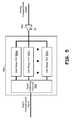
- FIG. 1is a system diagram illustrating various communication devices that include therein an Analog to Digital Converter (ADC) constructed and operating according to one or more embodiments of the present invention
- ADCAnalog to Digital Converter
- FIG. 2is a block diagram illustrating a Powerline Communication (PLC) device constructed according to one or more embodiments of the present invention
- FIG. 3illustrates a communication device having a configurable architecture and that includes at least one ADC constructed and operating according to one or more embodiments of the present invention
- FIG. 4is a block diagram illustrating a communication interface having an ADC constructed and operating according to one or more embodiments of the present invention
- FIG. 5is a block diagram illustrating an ADC constructed and operated according to one or more embodiments of the present invention.
- FIG. 6Ais a graph illustrating a full range of an analog communication signal operated on by an ADC constructed according to the present invention
- FIG. 6Bis a graph illustrating a full range of an analog communication signal operated on by an ADC constructed according to the present invention but with differing sub-range ADC span than that of FIG. 6A ;
- FIG. 7is a flowchart illustrating operations of an ADC constructed and operating according to one or more embodiments of the present invention.
- FIG. 8is a block diagram illustrating an ADC constructed according to another embodiment of the present invention that includes sub-range adjustment
- FIG. 9is a flowchart illustrating operations according to another embodiment of the present invention.
- FIG. 10is a block diagram illustrating an ADC constructed and operated according to one or more embodiments of the present invention.
- FIG. 11is a flowchart illustrating operations according to another embodiment of the present invention for ADC calibration.
- FIG. 1is a system diagram illustrating various communication devices that include therein an Analog to Digital Converter (ADC) constructed and operating according to one or more embodiments of the present invention.
- the communication devices of FIG. 1include an ADC that operates upon one or more communication signals.
- the ADC of the present inventionmay also operate upon signals other than communication signals.
- the communication devices illustrated in FIG. 1include a handheld communication device 102 , a wireless router 104 , a wired router 106 , a set top box/video player/audio-video device 108 , laptop computer 110 , desktop computer 112 , or a base station 114 .
- Other devices than those shownmay also include an ADC constructed and operating according to the present invention.
- the handheld device 102may be a cellular telephone that communicates with a cellular network via one or more radio interfaces, a Personal Data Assistant, a handheld data terminal, or another hand held device.
- the handheld device 102may also service Wireless Local Area Network (WLAN) communications, Wireless Personal Area Network (WPAN) communications, Global Positioning System (GPS) operations, 60 GHz operations, infrared operations, and/or other communications operations.
- the wireless router 104includes both a wireless interface and a wired interface.
- the wireless router 104communicates wirelessly with a number of serviced client devices and may communicate with a remote device via a wired link.
- the wired linkmay be a cable modem communication link, an optical communication link, a Local Area Network (LAN) communication link or another communication link.
- the router 106routes communication signals via its ports among a plurality of remote devices.
- the set top box 108services home entertainment, streaming media, and/other communications within a home or premises.
- the set top box 108may stream content to televisions, multi-media systems, and/or other audio video devices.
- the laptop computer 110may include a cellular, WLAN, or WPAN communication link that services communications between the laptop computer 110 and one or more remote devices.
- the desktop computer 112may include a wired communication link and/or one more wireless communication links that service communications of the desktop computer 112 .
- Base station 114services a plurality of wirelessly coupled cellular telephones or Wireless Wide Area Network (WWAN) terminals within its service coverage area.
- WWANWireless Wide Area Network
- Each of the devices 102 - 114 illustrated in FIG. 1includes an ADC constructed and operated according to one or more embodiments of the present invention.
- the ADCis operable to receive analog communication signals and to convert the analog communication signals to digital communication signals.
- the ADC of the present inventionis operable to receive non-communication analog signals and to convert the analog signals to digital signals.
- FIG. 2is a block diagram illustrating a Powerline Communication (PLC) device constructed according to one or more other embodiments of the present invention.
- the PLC device 200supports PLC operations according to one or more PLC communication standards.
- the PLC device 200may be permanently installed within a home or other premises.
- the PLC deviceis mobile and services powerline communications when plugged into a wall plug and when one or more devices is available for paired communication via the wall plug.
- the PLC device 200includes a PLC interface 206 that includes a power plug interface 208 , an Analog Front End (AFE) 210 , and a Digital Front End (DFE) 212 .
- AFEAnalog Front End
- DFEDigital Front End
- the AFE 210includes analog signal processing elements while the DFE 212 includes digital signal processing elements.
- At least one Analog to Digital Converter (ADC) and at least one Digital to Analog Converter (DAC)service analog to digital and digital to analog signal conversion operations, respectively.
- ADC of the PLC interface 206is constructed and operates according to one or more embodiments of the present invention.
- the PLC device 200also includes one or more other communication interfaces, including a WWAN interface 214 , e.g., a WiMAX interface, a WLAN interface 216 , e.g., an 802.11x interface, a WPAN interface 218 , e.g., a Bluetooth interface, a 60 GHz interface 220 (millimeter wave interface), a LAN interface 222 , e.g., an Ethernet interface, a cable interface 224 , e.g.
- a WWAN interface 214e.g., a WiMAX interface
- WLAN interface 216e.g., an 802.11x interface
- WPAN interface 218e.g., a Bluetooth interface
- 60 GHz interface 220millimeter wave interface
- a LAN interface 222e.g., an Ethernet interface
- cable interface 224e.g.
- MoCAMultimedia over Coax Alliance
- optical interface 226an optical interface 226 , a Near Field Communication (NFC) I/F 228 , an Infra-Red I/F 230 , and/or an RF Tag I/F 232 .
- NFCNear Field Communication
- Infra-Red I/F 230an RF Tag I/F 232 .
- the PLC device 200may bridge communications between a power plug and one or more devices, e.g., between the power plug and a desktop computer, a laptop computer, a touchpad computer, an appliance, a television, another entertainment system device, etc., via the PLC interface 206 and one or more of the other communication interfaces 214 , 216 , 218 , 220 , 222 , 224 , 226 , 228 , 230 , and/or 232 .
- the processing module 202may include one or more of a system processor, a digital signal processor, a processing module, dedicated hardware, an application specific integrated circuit (ASIC), or other circuitry that is capable of executing software instructions and for processing data.
- the processing module 202is operable to support Medium Access Control (MAC) management, communications bridging management, and other management of the communications circuitry of the PLC device 200 .
- the memory 204may be RAM, ROM, FLASH RAM, FLASH ROM, optical memory, magnetic memory, or other types of memory that is capable of storing data and/or instructions in allowing processing circuitry to access same.
- Each of the communication interfaces of the PLC device 200 of FIG. 2may include an ADC constructed and operating according to one or more embodiments of the present invention.
- the AFE 210 or DFE 212 of the PLC interface 206 of the PLC communication device 200will include an ADC that converts communication signals between an analog format and a digital format.
- each of the other communication interfaces 214 - 232may also include an ADC constructed and operating according to one or more embodiments of the present invention. The manner in which the ADC of the present invention operates upon communication signals will be described further herein with reference to the subsequent FIGs.
- FIG. 3illustrates a communication device having a configurable architecture and that includes at least one ADC constructed and operating according to one or more embodiments of the present invention.
- the PLC device 300includes a processing module 302 and memory 304 that may have a structure similar or same as like named components of FIG. 2 .
- the PLC device 300further includes a DFE 306 and an AFE 308 that may have a structure similar or same as like named components of FIG. 2 .
- the PLC device 300further includes a switch matrix 310 that intercouples the AFE 308 to a PLC I/F 312 , a LAN I/F 314 , a MoCA I/F 316 , and a Wireless I/F 318 .
- the PLC device 300 or communication device 300 of FIG. 3includes one or more ADCs constructed and operating according to the present invention to convert an analog signal to a digital signal.
- the ADCwould be present in either the DFE 306 or AFE 308 to link the two components together via analog to digital signal conversion.
- the ADC of the present inventionwould service communication signals received by each of the particular media coupled to the PLC device 300 .
- an analog communication signal coupled to the powerline media at power plugis received via the power plug interface 312 and relayed to AFE 308 via switch matrix 310 .
- the ADC of the present inventionAfter processing of the analog communication signal by AFE 308 , the ADC of the present invention would convert the analog communication signal to a digital communication signal.
- an analog communication signalcould be linked by LAN interface 314 from Ethernet cabling via switch matrix 310 to AFE 308 .
- This communication signal that is an Ethernet type signalwould be processed by AFE 308 and converted to a digital communication signal by the ADC operating according to present invention.
- communication signals received via MoCA interface 316 or wireless interface 318may be coupled by switch matrix 310 to AFE 308 for further processing and then subsequent conversion by a DFE constructed and operating according to the present invention to convert the analog communication signal to a digital communication signal.
- FIG. 4is a block diagram illustrating a communication interface having an ADC constructed and operating according to one or more embodiments of the present invention.
- the communication interface 400is generically shown to include an analog front end 402 that receives analog signals from and transmits analog communication signals to a media/antenna/infrared interface, or another coupling element.
- the analog front end 402processes incoming analog communication signals and also processes outgoing analog communication signals prior to coupling the outgoing analog communication signals to the media.
- the digital front end 408processes digital communication signals both incoming and outgoing.
- the DFE 408couples to host processing circuitry and services the communications needs of the host processing circuitry.
- a digital to analog converter (DAC) 406receives outgoing digital signals from the DFE 408 , converts the outgoing digital signals to outgoing analog signals, and couples the outgoing analog signals to the AFE 402 .
- ADC 404receives analog communication signals from the AFE 402 and converts the analog communication signals to digital communication signals and couples the digital communication signals to the DFE 408 .
- the ADC 404 of the communications interface 400 of FIG. 4is constructed and operates according to one or more embodiments of the present invention as will be more fully described herein with reference to FIG. 5 through FIG. 9 .
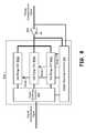
- FIG. 5is a block diagram illustrating an ADC constructed and operated according to one or more embodiments of the present invention.
- the ADC 500includes a plurality of sub-range ADCs 502 a , 502 b , and 502 n .
- Each of the sub-range ADCs 502 a , 502 b , and 502 nmeasures an analog communication signal across at least one respective sub-range of a full range serviced by the ADC 500 .
- the plurality of sub-rangesextend across the full range with a central sub-range ADC, e.g. ADC 502 b , having a smaller quantization step size and, resultantly, greater quantization accuracy than at least one other sub-range ADC, e.g.
- the ADC 500further includes signal combining circuitry 504 that is operable to process outputs of the plurality of sub-range ADCs 502 a , 502 b , and 502 n to create a digital communication signal.
- the ADC 500 of FIG. 5may be included with a communication device that also has a processing module, memory, and a communication interface.
- the ADC 500 of FIG. 5links an AFE and a DFE of the communication device.
- the AFEproduces an analog communication signal to the ADC and the DFE receives the digital communication signal from the ADC.
- the AFEcouples to an antenna, a physical media, or to another interface and processes an incoming signal to produce the analog communication signal.
- the DFEfurther processes the digital communication signal received from the ADC 500 and produces data therefrom and couples such data for output.
- the DACor other components of a communication interface according to various aspects of prior art.
- a central sub-range of the ADC 500 of FIG. 5may correspond to an expected range of the analog communication signal.
- the central sub-rangemay correspond to approximately a middle quarter of the full range.
- a first sub-rangemay extend from an upper portion of the central sub-range to an upper portion of the full range and a second sub-range extends from a lower portion of the central sub-range to a lower portion of the full range.
- the AFE that includes the ADC 500may include a programmable gain amplifier (PGA) 506 that is responsive to a gain input and operable to gain adjust the analog communication signal.
- Gain control circuitryis operable to produce the gain input to the PGA 506 so that the analog communication signal will fall within the expected range.
- the central sub-range ADC 502 bhas greater quantization accuracy by virtue of having a smaller quantization step size than at least one other sub-range ADC, 502 a , or 502 n .
- central sub-range ADC 502 bhas at least one more bit of resolution than sub-range ADCs 502 a and 502 n .
- the central sub range ADC 502 bhas a smaller quantization step size and a greater quantization accuracy than the outer sub-range ADCs 502 a and 502 n.
- the central sub-rangeis narrower than the total range covered by the outer sub-range(s).
- the central sub-range ADChas the same bit resolution as does the sub-range ADC(s) corresponding to the outer sub-range(s).
- the central sub-range ADC 502 bhas a smaller quantization step size and a greater quantization accuracy than the sub-range ADCs 502 a and 502 n covering the outer sub-ranges because its central sub-range is narrower than the outer sub-ranges.
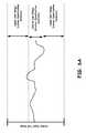
- the ADC 500 of FIG. 5may be implemented to perform sampling consistently with either FIG. 6A or FIG. 6B .
- FIG. 6Ais a graph illustrating a full range of an analog communication signal operated on by an ADC constructed according to the present invention.
- the analog communication signalprimarily resides within a central sub-range serviced by a central sub-range ADC that has greater quantization accuracy (smaller quantization step sizes) than the upper sub-range lower sub-range ADCs that service corresponding upper and lower sub-ranges.
- quantization accuracysmall quantization step sizes
- the discernibility inaccuracy of measuring the analog communication signalis greater.
- a digital communication signalis output from an ADC of the present invention with full range but will have greater resolution and resultantly a greater bandwidth of digital communication signal that provides higher performance for subsequent processing.
- a wide band communication signalis sampled by the ADC. It is important to have a wide bandwidth representation of this analog communication signal so as to not lose information, e.g. due to higher order modulations employed and a great number of tones in an OFDM front end, for example.
- the greater bit density of the central sub-rangeallows the ADC of the present invention to have a wide bandwidth and still a full range representation of the digital communication signal without the timing errors that are prevalent in prior art ADCs.
- FIG. 6Bis a graph illustrating a full range of an analog communication signal operated on by an ADC constructed according to the present invention.
- the analog communication signalprimarily resides within a central sub-range serviced by a central sub-range ADC.
- a single sub-range ADCsamples across all of the full range and its output is used when the signal does not reside within the central sub-range ADC.
- an ADCincludes two sub-range ADCs.
- a central sub-range ADCspans the central 1 ⁇ 4 of the full range and the other sub-range ADC covers the full range (two sub-ranges that do not correspond to the central sub-range).
- ADCs 502 a (full range) and 502 b (central sub-range)may be 6-bit converters (with 64 unique quantization levels) with the central-range ADC 502 b corresponding to 1 ⁇ 4 of the full range and ADC 502 a corresponding to the full range.
- the central sub-range ADC 502 bcovers 1 ⁇ 4 of the range that ADC 502 a covers, its step size and quantization accuracy is effectively 4 times greater than that of ADC 502 b .
- the ADC 500 output(digital communication signal) is an 8-bit digital signal for the central range while only being a 6-bit digital signal outside of the central range. Such is the case because the two most significant bits of an 8 bit output for the central range are known and constant.
- the ADC 500 outputis, effectively, the output of the ADC 502 b when the communication signal resides within the central sub-range and is the output of the ADC 502 a when the communication signal resides outside of the central sub-range.
- the impulse noise eventcauses the analog communication signal to be in one or more of the outer sub-ranges of the full range (corresponding to sub-range ADC with lower resolution) but not to clip the output of the ADC (composite of sub-range ADCs), meaning the outcome of the impulse noise event is a slight momentary loss of accuracy and but not clipped, which is a much preferable operating condition.
- the PGAmay be calibrated for normal operation without clipping caused by the impulse noise event, resulting implementing resistance to impulse noise events.
- FIG. 7is a flowchart illustrating operations 700 of an ADC constructed and operating according to one or more embodiments of the present invention.
- Operations 700commence with calibrating a programmable gain amplifier (PGA) for expected analog communication signal range (Step 702 ).
- PGAprogrammable gain amplifier
- a PGA 506is to be calibrated so that saturation will not occur across the full range of the ADC and so that the communication signal primarily resides within the central sub-range.
- DC offsetmay also be included in the calibration of the PGA as well as gain at Step 702 .
- the gain of the PGA and DC offsetmay be two separate settings for the PGA to ensure that the ADC operates as efficiently as possible to produce as accurate of a representation of the analog communication signal within the digital communication signal as possible.
- Step 704operation 700 continues with the sub-range ADCs sampling the analog communication signal (Step 704 ).
- the ADCsamples the communication signal using a plurality of sub-range ADCs with each sub-range ADC measuring the analog communication signal across a respective sub-range of the full range.
- the plurality of sub-rangesextends across the full range with a central sub-range ADC having greater quantization accuracy (smaller quantization step size) than at least one other sub-range ADC.
- Step 706produces a plurality of ADC outputs from the plurality of sub-range ADCs.
- Operationproceeds at Step 708 where signal combining circuitry produces the digital communication signal from the plurality of outputs of the plurality of sub-range ADCs.
- FIG. 8is a block diagram illustrating an ADC constructed according to another embodiment of the present invention that includes sub-range adjustment.
- the ADC 800includes sub-range ADCs 802 a , 802 b , and, optionally, 802 c .
- Each of the sub-range ADCs 802 a , 802 b , and 802 csamples the communication signal across a respective sub-range of the full range of the analog communication signal.
- the analog communication signalis operated upon by PGA 806 prior to providing the analog communication signal to each of the sub-range ADCs 802 a , 802 b , and 802 c .
- the outputs of the sub-range ADCs 802 a , 802 b , and 802 care received by signal combining circuitry 804 that produces a digital communication signal based upon such outputs.
- the sub-ranges serviced by the plurality of sub-range ADCs 802 a , 802 b , and 802 care adjusted over time based upon the expected characteristics of the analog communication signal.
- the range of the analog communication signalmay vary over time such that the central range may be adjusted to be wider or narrower.
- the ADC 800may do a better job of sampling the analog communication signal to produce the digital communication signal.
- FIG. 9is a flowchart illustrating operations according to another embodiment of the present invention.
- Operations 900commence with the ADC determining a number of sub-range ADCs to employ for sampling (Step 902 ).
- Operation 900continues with calibrating the PGA for expected analog communication signal range (Step 904 ).
- the operationthen proceeds to selecting the particular sub-range ADCs to be used for signal sampling (Step 906 ).
- Step 908a particular signal range to be sampled by each sub-range ADC is selected (Step 908 ).
- the ADCsamples an analog signal using the enabled sub-range ADCs (Step 910 ). Sampling will continue until it is determined to re-provision the sub-range ADCs at Step 912 , where reprovisioning will cause operation to return to Step 902 .
- FIG. 10is a block diagram illustrating an ADC constructed and operated according to one or more embodiments of the present invention.
- the ADC 1000includes a plurality of sub-range ADCs 1002 a , 1002 b , and, optionally, 1002 c .
- Each of the sub-range ADCs 1002 a , 1002 b , and 1002 cmeasures an analog communication signal across a respective sub-range of a full range serviced by the ADC 1000 .
- the plurality of sub-rangesextend across the full range with a central sub-range ADC, e.g. ADC 1002 b , having a greater quantization step size and, resultantly, quantization accuracy than at least one other sub-range ADC, e.g.
- the ADC 1000further includes signal combining circuitry 1004 that is operable to process outputs of the plurality of sub-range ADCs 1002 a , 1002 b , and 1002 c to create a digital communication signal.
- the ADC 1000 of FIG. 10is similar in construct and operation to the ADC 500 of FIG. 5 , except that each sub-range ADCs 1002 a , 1002 b , and 1002 c of FIG. 10 each include respective PGAs 1006 a , 1006 b , and 1006 c . Further, the ADC 1000 includes calibration circuitry 1008 operable to calibrate the ADC 100 by providing gain settings to each of the PGAs 1006 a , 1006 b , and 1006 c . The ADC 1000 of FIG. 10 may also include the range adjustment features of the ADC 800 of FIG. 8 in some embodiments. The gain settings Ga, Gb, and Gc provided to sub-range ADCs 1002 a , 1002 b , and 1002 c may include both gain and DC offset components.
- FIG. 11is a flowchart illustrating operations according to another embodiment of the present invention for ADC calibration.
- ADC of the present inventionmatching the gain and offset of each sub-range ADC exactly to a desired level must be performed to maintain accuracy, i.e., how does the central sub-range ADC sample exactly 1 ⁇ 4 of the full range (corresponding to another sub-range ADC in some embodiments), for example.
- cross-rangingis employed for such calibration operations.
- Cross-rangingtakes advantage of the fact that the analog communication signal may, at any time, be in the range of multiple sub-range ADCs.
- the analog communication signalis being quantized by more than one ADC at the same time, e.g., valid digital samples are produced by multiple sub-range ADCs simultaneously. In theory these two results should be identical. If not, it points to gain or offset error in one of the sub-range ADCs.
- the idea hereis that the over-ranging sections of the signal can be used to calibrate the sub-range ADCs while the ADC is fully operating.
- Operations 1100commence with monitoring the outputs of the sub-range ADCs (Step 1102 ). Upon measuring the outputs of the sub-range ADCs, operations include determining whether the outputs of two of the sub-range ADCs overlap (Step 1102 ). If the outputs do not overlap, operations return to Step 1102 . However, if the outputs of two of the sub-range ADCs overlap as determined at Step 1104 it is next determined whether the outputs of the two sub-range ADCs match (Step 1106 ). Determining whether the outputs of the two sub-range ADCs match is determined within a selected tolerance.
- the methodincludes adjusting the gain/DC offset of one or more PGAs of the ADC and/or adjusting one or both of the sub-range ADCs. From Step 1108 operation returns to Step 1102 .
- circuitand “circuitry” as used herein may refer to an independent circuit or to a portion of a multifunctional circuit that performs multiple underlying functions.
- processing circuitrymay be implemented as a single chip processor or as a plurality of processing chips.
- a first circuit and a second circuitmay be combined in one embodiment into a single circuit or, in another embodiment, operate independently perhaps in separate chips.
- chiprefers to an integrated circuit. Circuits and circuitry may comprise general or specific purpose hardware, or may comprise such hardware and associated software such as firmware or object code.
- the terms “substantially” and “approximately”provides an industry-accepted tolerance for its corresponding term and/or relativity between items. Such an industry-accepted tolerance ranges from less than one percent to fifty percent and corresponds to, but is not limited to, component values, integrated circuit process variations, temperature variations, rise and fall times, and/or thermal noise. Such relativity between items ranges from a difference of a few percent to magnitude differences.
- the term(s) “coupled to” and/or “coupling” and/orincludes direct coupling between items and/or indirect coupling between items via an intervening item (e.g., an item includes, but is not limited to, a component, an element, a circuit, and/or a module) where, for indirect coupling, the intervening item does not modify the information of a signal but may adjust its current level, voltage level, and/or power level.
- an intervening iteme.g., an item includes, but is not limited to, a component, an element, a circuit, and/or a module
Landscapes
- Engineering & Computer Science (AREA)
- Computer Networks & Wireless Communication (AREA)
- Signal Processing (AREA)
- Theoretical Computer Science (AREA)
- Power Engineering (AREA)
- Cable Transmission Systems, Equalization Of Radio And Reduction Of Echo (AREA)
- Analogue/Digital Conversion (AREA)
- Small-Scale Networks (AREA)
- Mobile Radio Communication Systems (AREA)
- Selective Calling Equipment (AREA)
Abstract
Description
Claims (23)
Priority Applications (2)
| Application Number | Priority Date | Filing Date | Title |
|---|---|---|---|
| US13/246,308US8483291B2 (en) | 2011-06-30 | 2011-09-27 | Analog to digital converter with increased sub-range resolution |
| US13/925,239US8711952B2 (en) | 2011-06-30 | 2013-06-24 | Analog to digital converter with increased sub-range resolution |
Applications Claiming Priority (2)
| Application Number | Priority Date | Filing Date | Title |
|---|---|---|---|
| US201161503060P | 2011-06-30 | 2011-06-30 | |
| US13/246,308US8483291B2 (en) | 2011-06-30 | 2011-09-27 | Analog to digital converter with increased sub-range resolution |
Related Child Applications (1)
| Application Number | Title | Priority Date | Filing Date |
|---|---|---|---|
| US13/925,239ContinuationUS8711952B2 (en) | 2011-06-30 | 2013-06-24 | Analog to digital converter with increased sub-range resolution |
Publications (2)
| Publication Number | Publication Date |
|---|---|
| US20130003873A1 US20130003873A1 (en) | 2013-01-03 |
| US8483291B2true US8483291B2 (en) | 2013-07-09 |
Family
ID=47390618
Family Applications (9)
| Application Number | Title | Priority Date | Filing Date |
|---|---|---|---|
| US13/246,308ActiveUS8483291B2 (en) | 2011-06-30 | 2011-09-27 | Analog to digital converter with increased sub-range resolution |
| US13/246,585AbandonedUS20130003875A1 (en) | 2011-06-30 | 2011-09-27 | Powerline communication device with multiple plc interface(s) |
| US13/329,474AbandonedUS20130003876A1 (en) | 2011-06-30 | 2011-12-19 | Breaker box powerline communication device |
| US13/431,034AbandonedUS20130003696A1 (en) | 2011-06-30 | 2012-03-27 | Device handing over communication session from wireless communication to powerline communication |
| US13/432,144Active2032-05-23US9065465B2 (en) | 2011-06-30 | 2012-03-28 | PLC/wireless device coordinated wireless transmissions |
| US13/436,170ActiveUS8711951B2 (en) | 2011-06-30 | 2012-03-30 | Powerline communication device with load characterization functionality |
| US13/434,908ActiveUS8750392B2 (en) | 2011-06-30 | 2012-03-30 | PLC device supporting MIMO operations |
| US13/477,424Expired - Fee RelatedUS8837606B2 (en) | 2011-06-30 | 2012-05-22 | Powerline communication device noise timing based operations |
| US13/925,239ActiveUS8711952B2 (en) | 2011-06-30 | 2013-06-24 | Analog to digital converter with increased sub-range resolution |
Family Applications After (8)
| Application Number | Title | Priority Date | Filing Date |
|---|---|---|---|
| US13/246,585AbandonedUS20130003875A1 (en) | 2011-06-30 | 2011-09-27 | Powerline communication device with multiple plc interface(s) |
| US13/329,474AbandonedUS20130003876A1 (en) | 2011-06-30 | 2011-12-19 | Breaker box powerline communication device |
| US13/431,034AbandonedUS20130003696A1 (en) | 2011-06-30 | 2012-03-27 | Device handing over communication session from wireless communication to powerline communication |
| US13/432,144Active2032-05-23US9065465B2 (en) | 2011-06-30 | 2012-03-28 | PLC/wireless device coordinated wireless transmissions |
| US13/436,170ActiveUS8711951B2 (en) | 2011-06-30 | 2012-03-30 | Powerline communication device with load characterization functionality |
| US13/434,908ActiveUS8750392B2 (en) | 2011-06-30 | 2012-03-30 | PLC device supporting MIMO operations |
| US13/477,424Expired - Fee RelatedUS8837606B2 (en) | 2011-06-30 | 2012-05-22 | Powerline communication device noise timing based operations |
| US13/925,239ActiveUS8711952B2 (en) | 2011-06-30 | 2013-06-24 | Analog to digital converter with increased sub-range resolution |
Country Status (1)
| Country | Link |
|---|---|
| US (9) | US8483291B2 (en) |
Cited By (2)
| Publication number | Priority date | Publication date | Assignee | Title |
|---|---|---|---|---|
| US8711952B2 (en)* | 2011-06-30 | 2014-04-29 | Broadcom Corporation | Analog to digital converter with increased sub-range resolution |
| US9654134B2 (en) | 2015-02-16 | 2017-05-16 | Sound Devices Llc | High dynamic range analog-to-digital conversion with selective regression based data repair |
Families Citing this family (202)
| Publication number | Priority date | Publication date | Assignee | Title |
|---|---|---|---|---|
| US20130051220A1 (en)* | 2011-08-22 | 2013-02-28 | Igor Ryshakov | Method and Apparatus for Quick-Switch Fault Tolerant Backup Channel |
| JP6019950B2 (en)* | 2011-09-13 | 2016-11-02 | ソニー株式会社 | Power supply apparatus and method, and program |
| US9160410B2 (en)* | 2011-10-31 | 2015-10-13 | Texas Instruments Incorporated | Coexistence method by requesting access to the channel |
| US8787283B2 (en)* | 2011-11-21 | 2014-07-22 | Maxlinear, Inc. | Method and system for providing reduced bandwidth acquisition latency |
| US8767554B2 (en)* | 2011-11-21 | 2014-07-01 | Maxlinear, Inc. | Method and system for optimizing bandwidth utilization in an in-home network |
| TW201328193A (en)* | 2011-12-23 | 2013-07-01 | Hon Hai Prec Ind Co Ltd | Conversion device for devices with COM interface |
| US9755852B2 (en)* | 2012-05-11 | 2017-09-05 | Fsr Inc. | Power over ethernet to USB adapter |
| US9480014B2 (en)* | 2012-06-01 | 2016-10-25 | Qualcomm Incorporated | Device configuration in a hybrid communication network |
| US9378073B2 (en) | 2012-08-14 | 2016-06-28 | International Business Machines Corporation | Remote procedure call for a distributed system |
| US10135492B2 (en)* | 2012-11-07 | 2018-11-20 | Texas Instruments Incorporated | Compatible communication between devices using different communication protocols |
| US9113347B2 (en) | 2012-12-05 | 2015-08-18 | At&T Intellectual Property I, Lp | Backhaul link for distributed antenna system |
| US10009065B2 (en) | 2012-12-05 | 2018-06-26 | At&T Intellectual Property I, L.P. | Backhaul link for distributed antenna system |
| US9008073B1 (en)* | 2012-12-07 | 2015-04-14 | Maxim Integrated Products, Inc. | Routing for power line communication systems |
| US20140192679A1 (en)* | 2013-01-08 | 2014-07-10 | Tatung Company | Convergent Network Node with the Automatic Reconfiguration Capability |
| CN104113488A (en)* | 2013-04-16 | 2014-10-22 | 中兴通讯股份有限公司 | Interface switching method and interface switching device |
| US20140355610A1 (en)* | 2013-05-31 | 2014-12-04 | Qualcomm Incorporated | Switched power line communication |
| US9999038B2 (en) | 2013-05-31 | 2018-06-12 | At&T Intellectual Property I, L.P. | Remote distributed antenna system |
| US9525524B2 (en) | 2013-05-31 | 2016-12-20 | At&T Intellectual Property I, L.P. | Remote distributed antenna system |
| CN104378266A (en)* | 2013-08-16 | 2015-02-25 | 中兴通讯股份有限公司 | Communication method and system for home network and PLC device |
| CN103631363B (en)* | 2013-09-22 | 2017-05-10 | 深圳市联和安业科技有限公司 | Automobile data interface expanding device and method for achieving data interaction |
| KR102102706B1 (en)* | 2013-10-01 | 2020-05-29 | 삼성전자주식회사 | Receiver of NFC device and NFC device |
| US8897697B1 (en) | 2013-11-06 | 2014-11-25 | At&T Intellectual Property I, Lp | Millimeter-wave surface-wave communications |
| CN104144200A (en)* | 2013-12-09 | 2014-11-12 | 腾讯科技(深圳)有限公司 | Communication methods, communication side and user side for internet of things |
| US9209902B2 (en) | 2013-12-10 | 2015-12-08 | At&T Intellectual Property I, L.P. | Quasi-optical coupler |
| US9137004B2 (en)* | 2013-12-12 | 2015-09-15 | Qualcomm Incorporated | Neighbor network channel reuse with MIMO capable stations |
| DE102013114563A1 (en)* | 2013-12-19 | 2015-06-25 | Valeo Schalter Und Sensoren Gmbh | A method for performing a parking operation of a motor vehicle in a transverse parking space, parking assistance system and motor vehicle |
| US9247435B2 (en)* | 2014-01-15 | 2016-01-26 | Qualcomm Incorporated | Null beamforming in a communication network |
| CN105323080B (en)* | 2014-06-09 | 2019-08-16 | 中兴通讯股份有限公司 | A kind of link backup, power supply backup method, apparatus and system |
| JP6421504B2 (en)* | 2014-07-28 | 2018-11-14 | ソニー株式会社 | Image processing apparatus and image processing method |
| DE102014012318B4 (en)* | 2014-08-19 | 2019-05-09 | Audi Ag | A method for predicting a consumption of a motor vehicle, motor vehicle and computer program |
| KR101827754B1 (en)* | 2014-08-25 | 2018-03-22 | 원 미디어, 엘엘씨 | Method for dynamic configuration of a flexible orthogonal frequency division multiplexing phy transport data frame preamble |
| US9692101B2 (en) | 2014-08-26 | 2017-06-27 | At&T Intellectual Property I, L.P. | Guided wave couplers for coupling electromagnetic waves between a waveguide surface and a surface of a wire |
| US9768833B2 (en) | 2014-09-15 | 2017-09-19 | At&T Intellectual Property I, L.P. | Method and apparatus for sensing a condition in a transmission medium of electromagnetic waves |
| US10063280B2 (en) | 2014-09-17 | 2018-08-28 | At&T Intellectual Property I, L.P. | Monitoring and mitigating conditions in a communication network |
| US9628854B2 (en) | 2014-09-29 | 2017-04-18 | At&T Intellectual Property I, L.P. | Method and apparatus for distributing content in a communication network |
| US9615269B2 (en) | 2014-10-02 | 2017-04-04 | At&T Intellectual Property I, L.P. | Method and apparatus that provides fault tolerance in a communication network |
| US9685992B2 (en)* | 2014-10-03 | 2017-06-20 | At&T Intellectual Property I, L.P. | Circuit panel network and methods thereof |
| US9503189B2 (en) | 2014-10-10 | 2016-11-22 | At&T Intellectual Property I, L.P. | Method and apparatus for arranging communication sessions in a communication system |
| US9762289B2 (en) | 2014-10-14 | 2017-09-12 | At&T Intellectual Property I, L.P. | Method and apparatus for transmitting or receiving signals in a transportation system |
| US9973299B2 (en) | 2014-10-14 | 2018-05-15 | At&T Intellectual Property I, L.P. | Method and apparatus for adjusting a mode of communication in a communication network |
| US9520945B2 (en) | 2014-10-21 | 2016-12-13 | At&T Intellectual Property I, L.P. | Apparatus for providing communication services and methods thereof |
| US9312919B1 (en) | 2014-10-21 | 2016-04-12 | At&T Intellectual Property I, Lp | Transmission device with impairment compensation and methods for use therewith |
| US9627768B2 (en) | 2014-10-21 | 2017-04-18 | At&T Intellectual Property I, L.P. | Guided-wave transmission device with non-fundamental mode propagation and methods for use therewith |
| US9653770B2 (en) | 2014-10-21 | 2017-05-16 | At&T Intellectual Property I, L.P. | Guided wave coupler, coupling module and methods for use therewith |
| US9577306B2 (en) | 2014-10-21 | 2017-02-21 | At&T Intellectual Property I, L.P. | Guided-wave transmission device and methods for use therewith |
| US9780834B2 (en) | 2014-10-21 | 2017-10-03 | At&T Intellectual Property I, L.P. | Method and apparatus for transmitting electromagnetic waves |
| US9769020B2 (en) | 2014-10-21 | 2017-09-19 | At&T Intellectual Property I, L.P. | Method and apparatus for responding to events affecting communications in a communication network |
| US9564947B2 (en) | 2014-10-21 | 2017-02-07 | At&T Intellectual Property I, L.P. | Guided-wave transmission device with diversity and methods for use therewith |
| US9461706B1 (en) | 2015-07-31 | 2016-10-04 | At&T Intellectual Property I, Lp | Method and apparatus for exchanging communication signals |
| US9544006B2 (en) | 2014-11-20 | 2017-01-10 | At&T Intellectual Property I, L.P. | Transmission device with mode division multiplexing and methods for use therewith |
| US10009067B2 (en) | 2014-12-04 | 2018-06-26 | At&T Intellectual Property I, L.P. | Method and apparatus for configuring a communication interface |
| US9997819B2 (en) | 2015-06-09 | 2018-06-12 | At&T Intellectual Property I, L.P. | Transmission medium and method for facilitating propagation of electromagnetic waves via a core |
| US10243784B2 (en) | 2014-11-20 | 2019-03-26 | At&T Intellectual Property I, L.P. | System for generating topology information and methods thereof |
| US9800327B2 (en) | 2014-11-20 | 2017-10-24 | At&T Intellectual Property I, L.P. | Apparatus for controlling operations of a communication device and methods thereof |
| US9954287B2 (en) | 2014-11-20 | 2018-04-24 | At&T Intellectual Property I, L.P. | Apparatus for converting wireless signals and electromagnetic waves and methods thereof |
| US9742462B2 (en) | 2014-12-04 | 2017-08-22 | At&T Intellectual Property I, L.P. | Transmission medium and communication interfaces and methods for use therewith |
| US9680670B2 (en) | 2014-11-20 | 2017-06-13 | At&T Intellectual Property I, L.P. | Transmission device with channel equalization and control and methods for use therewith |
| US10340573B2 (en) | 2016-10-26 | 2019-07-02 | At&T Intellectual Property I, L.P. | Launcher with cylindrical coupling device and methods for use therewith |
| US9654173B2 (en) | 2014-11-20 | 2017-05-16 | At&T Intellectual Property I, L.P. | Apparatus for powering a communication device and methods thereof |
| US10144036B2 (en) | 2015-01-30 | 2018-12-04 | At&T Intellectual Property I, L.P. | Method and apparatus for mitigating interference affecting a propagation of electromagnetic waves guided by a transmission medium |
| US9876570B2 (en) | 2015-02-20 | 2018-01-23 | At&T Intellectual Property I, Lp | Guided-wave transmission device with non-fundamental mode propagation and methods for use therewith |
| CN110661590B (en) | 2015-03-09 | 2021-04-20 | 第一媒体有限责任公司 | System Discovery and Signaling |
| US9749013B2 (en) | 2015-03-17 | 2017-08-29 | At&T Intellectual Property I, L.P. | Method and apparatus for reducing attenuation of electromagnetic waves guided by a transmission medium |
| US10224981B2 (en) | 2015-04-24 | 2019-03-05 | At&T Intellectual Property I, Lp | Passive electrical coupling device and methods for use therewith |
| US9705561B2 (en) | 2015-04-24 | 2017-07-11 | At&T Intellectual Property I, L.P. | Directional coupling device and methods for use therewith |
| US9793954B2 (en) | 2015-04-28 | 2017-10-17 | At&T Intellectual Property I, L.P. | Magnetic coupling device and methods for use therewith |
| US9871282B2 (en) | 2015-05-14 | 2018-01-16 | At&T Intellectual Property I, L.P. | At least one transmission medium having a dielectric surface that is covered at least in part by a second dielectric |
| US9748626B2 (en) | 2015-05-14 | 2017-08-29 | At&T Intellectual Property I, L.P. | Plurality of cables having different cross-sectional shapes which are bundled together to form a transmission medium |
| US9490869B1 (en) | 2015-05-14 | 2016-11-08 | At&T Intellectual Property I, L.P. | Transmission medium having multiple cores and methods for use therewith |
| US10650940B2 (en) | 2015-05-15 | 2020-05-12 | At&T Intellectual Property I, L.P. | Transmission medium having a conductive material and methods for use therewith |
| US10679767B2 (en) | 2015-05-15 | 2020-06-09 | At&T Intellectual Property I, L.P. | Transmission medium having a conductive material and methods for use therewith |
| US9917341B2 (en) | 2015-05-27 | 2018-03-13 | At&T Intellectual Property I, L.P. | Apparatus and method for launching electromagnetic waves and for modifying radial dimensions of the propagating electromagnetic waves |
| US9912381B2 (en) | 2015-06-03 | 2018-03-06 | At&T Intellectual Property I, Lp | Network termination and methods for use therewith |
| US10154493B2 (en) | 2015-06-03 | 2018-12-11 | At&T Intellectual Property I, L.P. | Network termination and methods for use therewith |
| US10103801B2 (en) | 2015-06-03 | 2018-10-16 | At&T Intellectual Property I, L.P. | Host node device and methods for use therewith |
| US10812174B2 (en) | 2015-06-03 | 2020-10-20 | At&T Intellectual Property I, L.P. | Client node device and methods for use therewith |
| US9866309B2 (en) | 2015-06-03 | 2018-01-09 | At&T Intellectual Property I, Lp | Host node device and methods for use therewith |
| US10348391B2 (en) | 2015-06-03 | 2019-07-09 | At&T Intellectual Property I, L.P. | Client node device with frequency conversion and methods for use therewith |
| US9913139B2 (en) | 2015-06-09 | 2018-03-06 | At&T Intellectual Property I, L.P. | Signal fingerprinting for authentication of communicating devices |
| US10142086B2 (en) | 2015-06-11 | 2018-11-27 | At&T Intellectual Property I, L.P. | Repeater and methods for use therewith |
| US9608692B2 (en) | 2015-06-11 | 2017-03-28 | At&T Intellectual Property I, L.P. | Repeater and methods for use therewith |
| US9820146B2 (en) | 2015-06-12 | 2017-11-14 | At&T Intellectual Property I, L.P. | Method and apparatus for authentication and identity management of communicating devices |
| US9667317B2 (en) | 2015-06-15 | 2017-05-30 | At&T Intellectual Property I, L.P. | Method and apparatus for providing security using network traffic adjustments |
| US9640850B2 (en) | 2015-06-25 | 2017-05-02 | At&T Intellectual Property I, L.P. | Methods and apparatus for inducing a non-fundamental wave mode on a transmission medium |
| US9509415B1 (en) | 2015-06-25 | 2016-11-29 | At&T Intellectual Property I, L.P. | Methods and apparatus for inducing a fundamental wave mode on a transmission medium |
| US9865911B2 (en) | 2015-06-25 | 2018-01-09 | At&T Intellectual Property I, L.P. | Waveguide system for slot radiating first electromagnetic waves that are combined into a non-fundamental wave mode second electromagnetic wave on a transmission medium |
| US10170840B2 (en) | 2015-07-14 | 2019-01-01 | At&T Intellectual Property I, L.P. | Apparatus and methods for sending or receiving electromagnetic signals |
| US10044409B2 (en) | 2015-07-14 | 2018-08-07 | At&T Intellectual Property I, L.P. | Transmission medium and methods for use therewith |
| US10033107B2 (en) | 2015-07-14 | 2018-07-24 | At&T Intellectual Property I, L.P. | Method and apparatus for coupling an antenna to a device |
| US10033108B2 (en) | 2015-07-14 | 2018-07-24 | At&T Intellectual Property I, L.P. | Apparatus and methods for generating an electromagnetic wave having a wave mode that mitigates interference |
| US9853342B2 (en) | 2015-07-14 | 2017-12-26 | At&T Intellectual Property I, L.P. | Dielectric transmission medium connector and methods for use therewith |
| US9882257B2 (en) | 2015-07-14 | 2018-01-30 | At&T Intellectual Property I, L.P. | Method and apparatus for launching a wave mode that mitigates interference |
| US10148016B2 (en) | 2015-07-14 | 2018-12-04 | At&T Intellectual Property I, L.P. | Apparatus and methods for communicating utilizing an antenna array |
| US9836957B2 (en) | 2015-07-14 | 2017-12-05 | At&T Intellectual Property I, L.P. | Method and apparatus for communicating with premises equipment |
| US9847566B2 (en) | 2015-07-14 | 2017-12-19 | At&T Intellectual Property I, L.P. | Method and apparatus for adjusting a field of a signal to mitigate interference |
| US10341142B2 (en) | 2015-07-14 | 2019-07-02 | At&T Intellectual Property I, L.P. | Apparatus and methods for generating non-interfering electromagnetic waves on an uninsulated conductor |
| US9722318B2 (en) | 2015-07-14 | 2017-08-01 | At&T Intellectual Property I, L.P. | Method and apparatus for coupling an antenna to a device |
| US10320586B2 (en) | 2015-07-14 | 2019-06-11 | At&T Intellectual Property I, L.P. | Apparatus and methods for generating non-interfering electromagnetic waves on an insulated transmission medium |
| US9628116B2 (en) | 2015-07-14 | 2017-04-18 | At&T Intellectual Property I, L.P. | Apparatus and methods for transmitting wireless signals |
| US10205655B2 (en) | 2015-07-14 | 2019-02-12 | At&T Intellectual Property I, L.P. | Apparatus and methods for communicating utilizing an antenna array and multiple communication paths |
| US10090606B2 (en) | 2015-07-15 | 2018-10-02 | At&T Intellectual Property I, L.P. | Antenna system with dielectric array and methods for use therewith |
| US9793951B2 (en) | 2015-07-15 | 2017-10-17 | At&T Intellectual Property I, L.P. | Method and apparatus for launching a wave mode that mitigates interference |
| US9608740B2 (en) | 2015-07-15 | 2017-03-28 | At&T Intellectual Property I, L.P. | Method and apparatus for launching a wave mode that mitigates interference |
| US10784670B2 (en) | 2015-07-23 | 2020-09-22 | At&T Intellectual Property I, L.P. | Antenna support for aligning an antenna |
| US9871283B2 (en) | 2015-07-23 | 2018-01-16 | At&T Intellectual Property I, Lp | Transmission medium having a dielectric core comprised of plural members connected by a ball and socket configuration |
| US9912027B2 (en) | 2015-07-23 | 2018-03-06 | At&T Intellectual Property I, L.P. | Method and apparatus for exchanging communication signals |
| US9948333B2 (en) | 2015-07-23 | 2018-04-17 | At&T Intellectual Property I, L.P. | Method and apparatus for wireless communications to mitigate interference |
| US9749053B2 (en) | 2015-07-23 | 2017-08-29 | At&T Intellectual Property I, L.P. | Node device, repeater and methods for use therewith |
| US9735833B2 (en) | 2015-07-31 | 2017-08-15 | At&T Intellectual Property I, L.P. | Method and apparatus for communications management in a neighborhood network |
| US10020587B2 (en) | 2015-07-31 | 2018-07-10 | At&T Intellectual Property I, L.P. | Radial antenna and methods for use therewith |
| US9967173B2 (en) | 2015-07-31 | 2018-05-08 | At&T Intellectual Property I, L.P. | Method and apparatus for authentication and identity management of communicating devices |
| US9904535B2 (en) | 2015-09-14 | 2018-02-27 | At&T Intellectual Property I, L.P. | Method and apparatus for distributing software |
| US9705571B2 (en) | 2015-09-16 | 2017-07-11 | At&T Intellectual Property I, L.P. | Method and apparatus for use with a radio distributed antenna system |
| US10051629B2 (en) | 2015-09-16 | 2018-08-14 | At&T Intellectual Property I, L.P. | Method and apparatus for use with a radio distributed antenna system having an in-band reference signal |
| US10136434B2 (en) | 2015-09-16 | 2018-11-20 | At&T Intellectual Property I, L.P. | Method and apparatus for use with a radio distributed antenna system having an ultra-wideband control channel |
| US10079661B2 (en) | 2015-09-16 | 2018-09-18 | At&T Intellectual Property I, L.P. | Method and apparatus for use with a radio distributed antenna system having a clock reference |
| US10009063B2 (en) | 2015-09-16 | 2018-06-26 | At&T Intellectual Property I, L.P. | Method and apparatus for use with a radio distributed antenna system having an out-of-band reference signal |
| US10009901B2 (en) | 2015-09-16 | 2018-06-26 | At&T Intellectual Property I, L.P. | Method, apparatus, and computer-readable storage medium for managing utilization of wireless resources between base stations |
| US9769128B2 (en) | 2015-09-28 | 2017-09-19 | At&T Intellectual Property I, L.P. | Method and apparatus for encryption of communications over a network |
| US9729197B2 (en) | 2015-10-01 | 2017-08-08 | At&T Intellectual Property I, L.P. | Method and apparatus for communicating network management traffic over a network |
| US9882277B2 (en) | 2015-10-02 | 2018-01-30 | At&T Intellectual Property I, Lp | Communication device and antenna assembly with actuated gimbal mount |
| US9876264B2 (en) | 2015-10-02 | 2018-01-23 | At&T Intellectual Property I, Lp | Communication system, guided wave switch and methods for use therewith |
| US10074890B2 (en) | 2015-10-02 | 2018-09-11 | At&T Intellectual Property I, L.P. | Communication device and antenna with integrated light assembly |
| US10051483B2 (en) | 2015-10-16 | 2018-08-14 | At&T Intellectual Property I, L.P. | Method and apparatus for directing wireless signals |
| US10355367B2 (en) | 2015-10-16 | 2019-07-16 | At&T Intellectual Property I, L.P. | Antenna structure for exchanging wireless signals |
| US10665942B2 (en) | 2015-10-16 | 2020-05-26 | At&T Intellectual Property I, L.P. | Method and apparatus for adjusting wireless communications |
| US20170126421A1 (en) | 2015-10-29 | 2017-05-04 | Not for Radio, LLC | Fixture data over powerline network |
| JP6791238B2 (en)* | 2016-02-22 | 2020-11-25 | コニカミノルタ株式会社 | Portable radiation imaging device |
| JP6546867B2 (en)* | 2016-03-10 | 2019-07-17 | 東京エレクトロン株式会社 | How to adjust the processing process |
| KR20170106862A (en)* | 2016-03-14 | 2017-09-22 | 삼성전자주식회사 | Method for synchronizing data and electronic apparatus and system implementing the same |
| US9912419B1 (en) | 2016-08-24 | 2018-03-06 | At&T Intellectual Property I, L.P. | Method and apparatus for managing a fault in a distributed antenna system |
| US9860075B1 (en) | 2016-08-26 | 2018-01-02 | At&T Intellectual Property I, L.P. | Method and communication node for broadband distribution |
| US10291311B2 (en) | 2016-09-09 | 2019-05-14 | At&T Intellectual Property I, L.P. | Method and apparatus for mitigating a fault in a distributed antenna system |
| US11032819B2 (en) | 2016-09-15 | 2021-06-08 | At&T Intellectual Property I, L.P. | Method and apparatus for use with a radio distributed antenna system having a control channel reference signal |
| US10135146B2 (en) | 2016-10-18 | 2018-11-20 | At&T Intellectual Property I, L.P. | Apparatus and methods for launching guided waves via circuits |
| US10135147B2 (en) | 2016-10-18 | 2018-11-20 | At&T Intellectual Property I, L.P. | Apparatus and methods for launching guided waves via an antenna |
| US10340600B2 (en) | 2016-10-18 | 2019-07-02 | At&T Intellectual Property I, L.P. | Apparatus and methods for launching guided waves via plural waveguide systems |
| US9991580B2 (en) | 2016-10-21 | 2018-06-05 | At&T Intellectual Property I, L.P. | Launcher and coupling system for guided wave mode cancellation |
| US10811767B2 (en) | 2016-10-21 | 2020-10-20 | At&T Intellectual Property I, L.P. | System and dielectric antenna with convex dielectric radome |
| US9876605B1 (en) | 2016-10-21 | 2018-01-23 | At&T Intellectual Property I, L.P. | Launcher and coupling system to support desired guided wave mode |
| US10374316B2 (en) | 2016-10-21 | 2019-08-06 | At&T Intellectual Property I, L.P. | System and dielectric antenna with non-uniform dielectric |
| US10312567B2 (en) | 2016-10-26 | 2019-06-04 | At&T Intellectual Property I, L.P. | Launcher with planar strip antenna and methods for use therewith |
| US10224634B2 (en) | 2016-11-03 | 2019-03-05 | At&T Intellectual Property I, L.P. | Methods and apparatus for adjusting an operational characteristic of an antenna |
| US10225025B2 (en) | 2016-11-03 | 2019-03-05 | At&T Intellectual Property I, L.P. | Method and apparatus for detecting a fault in a communication system |
| US10291334B2 (en) | 2016-11-03 | 2019-05-14 | At&T Intellectual Property I, L.P. | System for detecting a fault in a communication system |
| US10498044B2 (en) | 2016-11-03 | 2019-12-03 | At&T Intellectual Property I, L.P. | Apparatus for configuring a surface of an antenna |
| US10340601B2 (en) | 2016-11-23 | 2019-07-02 | At&T Intellectual Property I, L.P. | Multi-antenna system and methods for use therewith |
| US10340603B2 (en) | 2016-11-23 | 2019-07-02 | At&T Intellectual Property I, L.P. | Antenna system having shielded structural configurations for assembly |
| US10090594B2 (en) | 2016-11-23 | 2018-10-02 | At&T Intellectual Property I, L.P. | Antenna system having structural configurations for assembly |
| US10535928B2 (en) | 2016-11-23 | 2020-01-14 | At&T Intellectual Property I, L.P. | Antenna system and methods for use therewith |
| US10178445B2 (en) | 2016-11-23 | 2019-01-08 | At&T Intellectual Property I, L.P. | Methods, devices, and systems for load balancing between a plurality of waveguides |
| US10361489B2 (en) | 2016-12-01 | 2019-07-23 | At&T Intellectual Property I, L.P. | Dielectric dish antenna system and methods for use therewith |
| US10305190B2 (en) | 2016-12-01 | 2019-05-28 | At&T Intellectual Property I, L.P. | Reflecting dielectric antenna system and methods for use therewith |
| US10694379B2 (en) | 2016-12-06 | 2020-06-23 | At&T Intellectual Property I, L.P. | Waveguide system with device-based authentication and methods for use therewith |
| US10382976B2 (en) | 2016-12-06 | 2019-08-13 | At&T Intellectual Property I, L.P. | Method and apparatus for managing wireless communications based on communication paths and network device positions |
| US10326494B2 (en) | 2016-12-06 | 2019-06-18 | At&T Intellectual Property I, L.P. | Apparatus for measurement de-embedding and methods for use therewith |
| US10020844B2 (en) | 2016-12-06 | 2018-07-10 | T&T Intellectual Property I, L.P. | Method and apparatus for broadcast communication via guided waves |
| US9927517B1 (en) | 2016-12-06 | 2018-03-27 | At&T Intellectual Property I, L.P. | Apparatus and methods for sensing rainfall |
| US10439675B2 (en) | 2016-12-06 | 2019-10-08 | At&T Intellectual Property I, L.P. | Method and apparatus for repeating guided wave communication signals |
| US10819035B2 (en) | 2016-12-06 | 2020-10-27 | At&T Intellectual Property I, L.P. | Launcher with helical antenna and methods for use therewith |
| US10727599B2 (en) | 2016-12-06 | 2020-07-28 | At&T Intellectual Property I, L.P. | Launcher with slot antenna and methods for use therewith |
| US10135145B2 (en) | 2016-12-06 | 2018-11-20 | At&T Intellectual Property I, L.P. | Apparatus and methods for generating an electromagnetic wave along a transmission medium |
| US10755542B2 (en) | 2016-12-06 | 2020-08-25 | At&T Intellectual Property I, L.P. | Method and apparatus for surveillance via guided wave communication |
| US10637149B2 (en) | 2016-12-06 | 2020-04-28 | At&T Intellectual Property I, L.P. | Injection molded dielectric antenna and methods for use therewith |
| US10243270B2 (en) | 2016-12-07 | 2019-03-26 | At&T Intellectual Property I, L.P. | Beam adaptive multi-feed dielectric antenna system and methods for use therewith |
| US10446936B2 (en) | 2016-12-07 | 2019-10-15 | At&T Intellectual Property I, L.P. | Multi-feed dielectric antenna system and methods for use therewith |
| US10359749B2 (en) | 2016-12-07 | 2019-07-23 | At&T Intellectual Property I, L.P. | Method and apparatus for utilities management via guided wave communication |
| US10168695B2 (en) | 2016-12-07 | 2019-01-01 | At&T Intellectual Property I, L.P. | Method and apparatus for controlling an unmanned aircraft |
| US10139820B2 (en) | 2016-12-07 | 2018-11-27 | At&T Intellectual Property I, L.P. | Method and apparatus for deploying equipment of a communication system |
| US10389029B2 (en) | 2016-12-07 | 2019-08-20 | At&T Intellectual Property I, L.P. | Multi-feed dielectric antenna system with core selection and methods for use therewith |
| US10547348B2 (en) | 2016-12-07 | 2020-01-28 | At&T Intellectual Property I, L.P. | Method and apparatus for switching transmission mediums in a communication system |
| US9893795B1 (en) | 2016-12-07 | 2018-02-13 | At&T Intellectual Property I, Lp | Method and repeater for broadband distribution |
| US10027397B2 (en) | 2016-12-07 | 2018-07-17 | At&T Intellectual Property I, L.P. | Distributed antenna system and methods for use therewith |
| US10916969B2 (en) | 2016-12-08 | 2021-02-09 | At&T Intellectual Property I, L.P. | Method and apparatus for providing power using an inductive coupling |
| US10389037B2 (en) | 2016-12-08 | 2019-08-20 | At&T Intellectual Property I, L.P. | Apparatus and methods for selecting sections of an antenna array and use therewith |
| US10326689B2 (en) | 2016-12-08 | 2019-06-18 | At&T Intellectual Property I, L.P. | Method and system for providing alternative communication paths |
| US10601494B2 (en) | 2016-12-08 | 2020-03-24 | At&T Intellectual Property I, L.P. | Dual-band communication device and method for use therewith |
| US10938108B2 (en) | 2016-12-08 | 2021-03-02 | At&T Intellectual Property I, L.P. | Frequency selective multi-feed dielectric antenna system and methods for use therewith |
| US10530505B2 (en) | 2016-12-08 | 2020-01-07 | At&T Intellectual Property I, L.P. | Apparatus and methods for launching electromagnetic waves along a transmission medium |
| US9911020B1 (en) | 2016-12-08 | 2018-03-06 | At&T Intellectual Property I, L.P. | Method and apparatus for tracking via a radio frequency identification device |
| US10411356B2 (en) | 2016-12-08 | 2019-09-10 | At&T Intellectual Property I, L.P. | Apparatus and methods for selectively targeting communication devices with an antenna array |
| US10069535B2 (en) | 2016-12-08 | 2018-09-04 | At&T Intellectual Property I, L.P. | Apparatus and methods for launching electromagnetic waves having a certain electric field structure |
| US9998870B1 (en) | 2016-12-08 | 2018-06-12 | At&T Intellectual Property I, L.P. | Method and apparatus for proximity sensing |
| US10777873B2 (en) | 2016-12-08 | 2020-09-15 | At&T Intellectual Property I, L.P. | Method and apparatus for mounting network devices |
| US10103422B2 (en) | 2016-12-08 | 2018-10-16 | At&T Intellectual Property I, L.P. | Method and apparatus for mounting network devices |
| US10264586B2 (en) | 2016-12-09 | 2019-04-16 | At&T Mobility Ii Llc | Cloud-based packet controller and methods for use therewith |
| US10340983B2 (en) | 2016-12-09 | 2019-07-02 | At&T Intellectual Property I, L.P. | Method and apparatus for surveying remote sites via guided wave communications |
| US9838896B1 (en) | 2016-12-09 | 2017-12-05 | At&T Intellectual Property I, L.P. | Method and apparatus for assessing network coverage |
| US10312953B2 (en) | 2016-12-26 | 2019-06-04 | Industrial Technology Research Institute | Orthogonal frequency division multiplexing receiver with low-resolution analog to digital converter and electronic device thereof |
| KR20180098059A (en)* | 2017-02-24 | 2018-09-03 | 엘지전자 주식회사 | Mobile terminal |
| US9973940B1 (en) | 2017-02-27 | 2018-05-15 | At&T Intellectual Property I, L.P. | Apparatus and methods for dynamic impedance matching of a guided wave launcher |
| US10298293B2 (en) | 2017-03-13 | 2019-05-21 | At&T Intellectual Property I, L.P. | Apparatus of communication utilizing wireless network devices |
| US10103780B1 (en)* | 2017-03-31 | 2018-10-16 | GM Global Technology Operations LLC | Dual mode communication over automotive power lines |
| EP3404886A1 (en)* | 2017-05-15 | 2018-11-21 | IMEC vzw | Network stack for a plurality of physical communication interfaces |
| US10554235B2 (en)* | 2017-11-06 | 2020-02-04 | At&T Intellectual Property I, L.P. | Multi-input multi-output guided wave system and methods for use therewith |
| US10292111B1 (en)* | 2018-03-14 | 2019-05-14 | Corning Optical Communications LLC | Gain control circuit supporting dynamic gain control in a remote unit in a wireless distribution system (WDS) |
| CN108390700B (en)* | 2018-04-17 | 2024-05-14 | 东莞市慧眼数字技术有限公司 | Coupling device for feeding detection signal into high-voltage carrier wave |
| CN112602291B (en)* | 2018-08-27 | 2022-04-05 | 华为技术有限公司 | Communication device, system and method thereof |
| US20200145824A1 (en)* | 2018-11-05 | 2020-05-07 | Comcast Cable Communications, Llc | Localized Multi-Factor Network Authentication |
| IL263929A (en)* | 2018-12-24 | 2020-06-30 | S G A Innovations Ltd | Systems, devices, and methods for detecting and/or preventing communication over power lines |
| US10763918B1 (en) | 2019-06-10 | 2020-09-01 | Baker Hughes, A Ge Company, Llc | Time synchronization of bottom hole assembly components via powerline communication |
| CN113660691B (en)* | 2021-10-19 | 2022-03-11 | 国网江西省电力有限公司经济技术研究院 | Medium-voltage MIMO-PLC access terminal state monitoring device |
Citations (4)
| Publication number | Priority date | Publication date | Assignee | Title |
|---|---|---|---|---|
| US5250948A (en)* | 1991-12-19 | 1993-10-05 | Eastman Kodak Company | High level resolution enhancement for dual-range A/D conversion |
| US6285309B1 (en)* | 1999-09-14 | 2001-09-04 | Texas Instruments Incorporated | Nested pipelined analog-to-digital converter |
| US20070024484A1 (en)* | 2005-07-29 | 2007-02-01 | Song Liu | Reference voltage pre-charge in a multi-step sub-ranging analog-to-digital converter |
| US20100066583A1 (en)* | 2008-09-16 | 2010-03-18 | Electronics And Telecommunications Research Institute | Multi-stage successive approximation register analog-todigital converter and analog-to-digital converting method using the same |
Family Cites Families (48)
| Publication number | Priority date | Publication date | Assignee | Title |
|---|---|---|---|---|
| DE2402127C3 (en)* | 1974-01-17 | 1978-04-06 | Pluess-Staufer Ag, Oftringen (Schweiz) | Device for measuring the haze of surfaces |
| WO2001084806A2 (en)* | 2000-05-02 | 2001-11-08 | Phonex Broadband Corporation | Method and system for adapting a telephone line modem for use on the power line |
| US6870515B2 (en)* | 2000-12-28 | 2005-03-22 | Nortel Networks Limited | MIMO wireless communication system |
| US7194528B1 (en)* | 2001-05-18 | 2007-03-20 | Current Grid, Llc | Method and apparatus for processing inbound data within a powerline based communication system |
| JP4075461B2 (en)* | 2001-11-27 | 2008-04-16 | ソニー株式会社 | Communication system, communication terminal, and communication method |
| BR0306849A (en)* | 2002-01-09 | 2004-11-09 | Geir Monsen Vavik | Transponder, wireless and wire-based transponder system, and use of at least one transponder and transponder system |
| WO2003063380A2 (en)* | 2002-01-24 | 2003-07-31 | Matsushita Electric Industrial Co., Ltd. | Method of and system for power line carrier communications |
| US7308103B2 (en)* | 2003-05-08 | 2007-12-11 | Current Technologies, Llc | Power line communication device and method of using the same |
| US20050085259A1 (en)* | 2003-10-15 | 2005-04-21 | Conner W. S. | Technique to coordinate wireless network over a power line or other wired back channel |
| US20050181839A1 (en)* | 2004-02-17 | 2005-08-18 | Nokia Corporation | Devices and methods for simultaneous battery charging and data transmission in a mobile terminal |
| US7269403B1 (en)* | 2004-06-03 | 2007-09-11 | Miao George J | Dual-mode wireless and wired power line communications |
| US7675979B1 (en)* | 2004-07-20 | 2010-03-09 | Marvell International Ltd. | Methods, algorithms, software, circuits, architectures, and systems for improved communications over cyclostationary channels |
| US8290498B2 (en)* | 2004-07-28 | 2012-10-16 | Broadcom Corporation | Mobile handoff through multi-network simulcasting |
| US20060267788A1 (en)* | 2005-01-21 | 2006-11-30 | Delany George B | Method and apparatus for illuminating a wall plate |
| EP1770870B1 (en)* | 2005-10-03 | 2019-04-03 | Avago Technologies International Sales Pte. Limited | Powerline communication device and method |
| US20070076666A1 (en)* | 2005-10-03 | 2007-04-05 | Riveiro Juan C | Multi-Wideband Communications over Power Lines |
| WO2008032225A2 (en)* | 2006-03-21 | 2008-03-20 | Ranco Incorporated Of Delaware | Refrigeration monitor unit |
| US7929940B1 (en)* | 2006-04-18 | 2011-04-19 | Nextel Communications Inc. | System and method for transmitting wireless digital service signals via power transmission lines |
| JP5061111B2 (en)* | 2006-09-15 | 2012-10-31 | パナソニック株式会社 | Speech coding apparatus and speech coding method |
| GB2443234B8 (en)* | 2006-10-24 | 2009-01-28 | Innovision Res & Tech Plc | Near field RF communicators and near field RF communications enabled devices |
| US8489344B2 (en)* | 2007-02-09 | 2013-07-16 | Adaptive Spectrum And Signal Alignment, Inc. | Home network system augmentation with remote guidance and local set up and monitoring |
| JP2008270999A (en)* | 2007-04-18 | 2008-11-06 | Sony Corp | Communicating system and communication equipment |
| US8352768B2 (en)* | 2007-04-27 | 2013-01-08 | At&T Intellectual Property I, L.P. | Controlling power states of a peripheral device in response to user proximity |
| WO2008135982A2 (en)* | 2007-05-02 | 2008-11-13 | Coppergate Communications Ltd. | Multiple input, multiple output (mimo) communication system over in-premises wires |
| JP4922848B2 (en)* | 2007-06-28 | 2012-04-25 | オリンパス株式会社 | Portable terminal device and network connection control method |
| EP2019496B1 (en)* | 2007-07-23 | 2017-06-07 | Sony Corporation | Method for transmitting a signal between a transmitter and a receiver in a power line network, transmitter, receiver, power line communication modem and powerline communication system |
| US8325710B2 (en)* | 2007-08-09 | 2012-12-04 | Phybridge Inc. | Inline power system and method for network communications |
| EP3065303B1 (en)* | 2007-08-22 | 2019-01-02 | Sony Corporation | Method for transmitting a signal via a power line network, transmitter, receiver, power line communication modem and power line communication system |
| JP5328662B2 (en)* | 2007-10-02 | 2013-10-30 | パナソニック株式会社 | Electronic apparatus and image processing apparatus |
| JP4450061B2 (en)* | 2007-12-06 | 2010-04-14 | ソニー株式会社 | COMMUNICATION CONTROL METHOD, COMMUNICATION DEVICE, AND COMMUNICATION SYSTEM |
| US7791523B2 (en)* | 2008-10-28 | 2010-09-07 | Agere Systems, Inc. | Two-step sub-ranging analog-to-digital converter and method for performing two-step sub-ranging in an analog-to-digital converter |
| US20100111199A1 (en)* | 2008-11-06 | 2010-05-06 | Manu Sharma | Device and Method for Communicating over Power Lines |
| JP5278035B2 (en)* | 2009-02-25 | 2013-09-04 | ソニー株式会社 | COMMUNICATION DEVICE AND COMMUNICATION METHOD, COMPUTER PROGRAM, AND COMMUNICATION SYSTEM |
| JP2010212804A (en)* | 2009-03-06 | 2010-09-24 | Sony Corp | Communication device and communication method, computer program, and communication system |
| US8213868B2 (en)* | 2009-04-17 | 2012-07-03 | Lingna Holdings Pte., Llc | Exploiting multiple antennas for spectrum sensing in cognitive radio networks |
| TWI562554B (en)* | 2009-12-30 | 2016-12-11 | Sony Corp | Communications system and device using beamforming |
| EP2343856B1 (en)* | 2010-01-11 | 2018-12-19 | Lantiq Beteiligungs-GmbH & Co.KG | Dynamic multicode home networking modem device |
| US8675651B2 (en)* | 2010-01-18 | 2014-03-18 | Qualcomm Incorporated | Coexistence mechanism for non-compatible powerline communication devices |
| JP5526833B2 (en)* | 2010-02-05 | 2014-06-18 | ソニー株式会社 | Wireless power transmission device |
| BR112012021961A2 (en)* | 2010-03-01 | 2016-06-07 | Abb Research Ltd | wireless communication between two temporarily connected devices |
| JP4989745B2 (en)* | 2010-03-29 | 2012-08-01 | 株式会社バッファロー | Apparatus, method, and program for relaying communication |
| JP4977229B2 (en)* | 2010-03-30 | 2012-07-18 | 株式会社バッファロー | Apparatus, method, and program for relaying communication |
| US20110286152A1 (en)* | 2010-05-07 | 2011-11-24 | Automated Media Services, Inc. | Mechanical and electrical system for powering shelf-edge electronic displays in a retail environment |
| JP5204811B2 (en)* | 2010-07-30 | 2013-06-05 | 株式会社バッファロー | COMMUNICATION DEVICE FOR RADIO COMMUNICATION, RADIO COMMUNICATION SYSTEM, AND METHOD FOR RADIO COMMUNICATION |
| JP2012049602A (en)* | 2010-08-24 | 2012-03-08 | Buffalo Inc | Connection apparatus, and method for use in connection apparatus |
| JP2012073743A (en)* | 2010-09-28 | 2012-04-12 | Buffalo Inc | Communication device, server system, program |
| US8947257B2 (en)* | 2011-03-09 | 2015-02-03 | General Electric Company | Systems, methods, and apparatuses for reducing network congestion in a smart utility meter system |
| US8483291B2 (en)* | 2011-06-30 | 2013-07-09 | Broadcom Corporation | Analog to digital converter with increased sub-range resolution |
- 2011
- 2011-09-27USUS13/246,308patent/US8483291B2/enactiveActive
- 2011-09-27USUS13/246,585patent/US20130003875A1/ennot_activeAbandoned
- 2011-12-19USUS13/329,474patent/US20130003876A1/ennot_activeAbandoned
- 2012
- 2012-03-27USUS13/431,034patent/US20130003696A1/ennot_activeAbandoned
- 2012-03-28USUS13/432,144patent/US9065465B2/enactiveActive
- 2012-03-30USUS13/436,170patent/US8711951B2/enactiveActive
- 2012-03-30USUS13/434,908patent/US8750392B2/enactiveActive
- 2012-05-22USUS13/477,424patent/US8837606B2/ennot_activeExpired - Fee Related
- 2013
- 2013-06-24USUS13/925,239patent/US8711952B2/enactiveActive
Patent Citations (4)
| Publication number | Priority date | Publication date | Assignee | Title |
|---|---|---|---|---|
| US5250948A (en)* | 1991-12-19 | 1993-10-05 | Eastman Kodak Company | High level resolution enhancement for dual-range A/D conversion |
| US6285309B1 (en)* | 1999-09-14 | 2001-09-04 | Texas Instruments Incorporated | Nested pipelined analog-to-digital converter |
| US20070024484A1 (en)* | 2005-07-29 | 2007-02-01 | Song Liu | Reference voltage pre-charge in a multi-step sub-ranging analog-to-digital converter |
| US20100066583A1 (en)* | 2008-09-16 | 2010-03-18 | Electronics And Telecommunications Research Institute | Multi-stage successive approximation register analog-todigital converter and analog-to-digital converting method using the same |
Cited By (2)
| Publication number | Priority date | Publication date | Assignee | Title |
|---|---|---|---|---|
| US8711952B2 (en)* | 2011-06-30 | 2014-04-29 | Broadcom Corporation | Analog to digital converter with increased sub-range resolution |
| US9654134B2 (en) | 2015-02-16 | 2017-05-16 | Sound Devices Llc | High dynamic range analog-to-digital conversion with selective regression based data repair |
Also Published As
| Publication number | Publication date |
|---|---|
| US20130003877A1 (en) | 2013-01-03 |
| US8750392B2 (en) | 2014-06-10 |
| US8711952B2 (en) | 2014-04-29 |
| US8837606B2 (en) | 2014-09-16 |
| US9065465B2 (en) | 2015-06-23 |
| US8711951B2 (en) | 2014-04-29 |
| US20130007311A1 (en) | 2013-01-03 |
| US20130279609A1 (en) | 2013-10-24 |
| US20130003878A1 (en) | 2013-01-03 |
| US20130003873A1 (en) | 2013-01-03 |
| US20130003696A1 (en) | 2013-01-03 |
| US20130003876A1 (en) | 2013-01-03 |
| US20130003879A1 (en) | 2013-01-03 |
| US20130003875A1 (en) | 2013-01-03 |
Similar Documents
| Publication | Publication Date | Title |
|---|---|---|
| US8483291B2 (en) | Analog to digital converter with increased sub-range resolution | |
| US8754800B2 (en) | Methods and arrangements for high-speed analog-to-digital conversion | |
| TW535367B (en) | A calibrated dc compensation system for a wireless communication device configured in a zero intermediate frequency architecture | |
| TW529274B (en) | Packet acquisition and channel tracking for a wireless communication device configured in a zero intermediate frequency architecture | |
| US8310387B2 (en) | Sampling method for time-interleaved data converters in frequency-multiplexed communications systems | |
| US8565692B2 (en) | System and method for providing a versatile RF and analog front-end for wireless and wired networks | |
| JP5189837B2 (en) | Analog-digital converter, communication device using the same, and wireless transceiver | |
| US20140350872A1 (en) | Transmit power measurement apparatus having programmable filter device that is set at least based on frequency response of transmit power detection path and related transmit power measurement method thereof | |
| CN103236865B (en) | There is the split type microwave backhaul architecture of smart outdoor unit | |
| US20180102784A1 (en) | Method and system for gain control for time-interleaved analog-to-digital convertor (adc) | |
| US20070147488A1 (en) | Apparatus and method for communication between a digital unit and a remote RF unit in a broadband wireless communication system | |
| CN103098404A (en) | Method and apparatus for real time multiplexing with receiver and antenna array elements | |
| US9685970B1 (en) | Analog-to-digital converting system and converting method | |
| CN102301606A (en) | Method And Apparatus For Digitally Equalizing A Signal In A Distributed Antenna System | |
| EP2158683A1 (en) | Method and system for a configurable communication integrated circuit and/or chipset | |
| US7965215B2 (en) | Method and system for variable resolution data conversion in a receiver | |
| CN110460342B (en) | Gain compensation method | |
| US11539371B1 (en) | Digital-to-analog converter (DAC) calibration using error DACs | |
| CN101345540B (en) | Radio receiver circuit, radio transceiver circuit and calibration method thereof | |
| CN114826261B (en) | System and method for adaptive error cancellation of digital/analog conversion | |
| US20090154575A1 (en) | Method and system for adc calibration in ofdm systems | |
| TW202423057A (en) | Phase tracking and correction architecture | |
| US11770129B2 (en) | Pipelined analog-to-digital conversion | |
| US7049882B2 (en) | Transmitter IF section and method enabling IF output signal amplitude that is less sensitive to process, voltage, and temperature | |
| Madhow | MultiGigabit millimeter wave communication: System concepts and challenges |
Legal Events
| Date | Code | Title | Description |
|---|---|---|---|
| AS | Assignment | Owner name:BROADCOM CORPORATION, CALIFORNIA Free format text:ASSIGNMENT OF ASSIGNORS INTEREST;ASSIGNORS:FINDLATER, KEITH;DANESH, SEYED AA;HURWITZ, JONATHAN EPHRAIM DAVID;SIGNING DATES FROM 20110923 TO 20110927;REEL/FRAME:026979/0348 | |
| FEPP | Fee payment procedure | Free format text:PAYOR NUMBER ASSIGNED (ORIGINAL EVENT CODE: ASPN); ENTITY STATUS OF PATENT OWNER: LARGE ENTITY | |
| STCF | Information on status: patent grant | Free format text:PATENTED CASE | |
| AS | Assignment | Owner name:BANK OF AMERICA, N.A., AS COLLATERAL AGENT, NORTH CAROLINA Free format text:PATENT SECURITY AGREEMENT;ASSIGNOR:BROADCOM CORPORATION;REEL/FRAME:037806/0001 Effective date:20160201 Owner name:BANK OF AMERICA, N.A., AS COLLATERAL AGENT, NORTH Free format text:PATENT SECURITY AGREEMENT;ASSIGNOR:BROADCOM CORPORATION;REEL/FRAME:037806/0001 Effective date:20160201 | |
| FPAY | Fee payment | Year of fee payment:4 | |
| AS | Assignment | Owner name:AVAGO TECHNOLOGIES GENERAL IP (SINGAPORE) PTE. LTD., SINGAPORE Free format text:ASSIGNMENT OF ASSIGNORS INTEREST;ASSIGNOR:BROADCOM CORPORATION;REEL/FRAME:041706/0001 Effective date:20170120 Owner name:AVAGO TECHNOLOGIES GENERAL IP (SINGAPORE) PTE. LTD Free format text:ASSIGNMENT OF ASSIGNORS INTEREST;ASSIGNOR:BROADCOM CORPORATION;REEL/FRAME:041706/0001 Effective date:20170120 | |
| AS | Assignment | Owner name:BROADCOM CORPORATION, CALIFORNIA Free format text:TERMINATION AND RELEASE OF SECURITY INTEREST IN PATENTS;ASSIGNOR:BANK OF AMERICA, N.A., AS COLLATERAL AGENT;REEL/FRAME:041712/0001 Effective date:20170119 | |
| AS | Assignment | Owner name:AVAGO TECHNOLOGIES INTERNATIONAL SALES PTE. LIMITE Free format text:MERGER;ASSIGNOR:AVAGO TECHNOLOGIES GENERAL IP (SINGAPORE) PTE. LTD.;REEL/FRAME:047230/0133 Effective date:20180509 | |
| AS | Assignment | Owner name:AVAGO TECHNOLOGIES INTERNATIONAL SALES PTE. LIMITE Free format text:CORRECTIVE ASSIGNMENT TO CORRECT THE EFFECTIVE DATE OF MERGER TO 09/05/2018 PREVIOUSLY RECORDED AT REEL: 047230 FRAME: 0133. ASSIGNOR(S) HEREBY CONFIRMS THE MERGER;ASSIGNOR:AVAGO TECHNOLOGIES GENERAL IP (SINGAPORE) PTE. LTD.;REEL/FRAME:047630/0456 Effective date:20180905 | |
| MAFP | Maintenance fee payment | Free format text:PAYMENT OF MAINTENANCE FEE, 8TH YEAR, LARGE ENTITY (ORIGINAL EVENT CODE: M1552); ENTITY STATUS OF PATENT OWNER: LARGE ENTITY Year of fee payment:8 | |
| MAFP | Maintenance fee payment | Free format text:PAYMENT OF MAINTENANCE FEE, 12TH YEAR, LARGE ENTITY (ORIGINAL EVENT CODE: M1553); ENTITY STATUS OF PATENT OWNER: LARGE ENTITY Year of fee payment:12 |