US8482375B2 - Sputter deposition of cermet resistor films with low temperature coefficient of resistance - Google Patents
Sputter deposition of cermet resistor films with low temperature coefficient of resistanceDownload PDFInfo
- Publication number
- US8482375B2 US8482375B2US12/786,238US78623810AUS8482375B2US 8482375 B2US8482375 B2US 8482375B2US 78623810 AUS78623810 AUS 78623810AUS 8482375 B2US8482375 B2US 8482375B2
- Authority
- US
- United States
- Prior art keywords
- anneal
- cermet
- films
- resistance
- ambient
- Prior art date
- Legal status (The legal status is an assumption and is not a legal conclusion. Google has not performed a legal analysis and makes no representation as to the accuracy of the status listed.)
- Active, expires
Links
Images


Classifications
- H—ELECTRICITY
- H01—ELECTRIC ELEMENTS
- H01C—RESISTORS
- H01C17/00—Apparatus or processes specially adapted for manufacturing resistors
- H01C17/06—Apparatus or processes specially adapted for manufacturing resistors adapted for coating resistive material on a base
- H01C17/075—Apparatus or processes specially adapted for manufacturing resistors adapted for coating resistive material on a base by thin film techniques
- H01C17/12—Apparatus or processes specially adapted for manufacturing resistors adapted for coating resistive material on a base by thin film techniques by sputtering
- H—ELECTRICITY
- H01—ELECTRIC ELEMENTS
- H01C—RESISTORS
- H01C17/00—Apparatus or processes specially adapted for manufacturing resistors
- H01C17/06—Apparatus or processes specially adapted for manufacturing resistors adapted for coating resistive material on a base
- H01C17/075—Apparatus or processes specially adapted for manufacturing resistors adapted for coating resistive material on a base by thin film techniques
- H—ELECTRICITY
- H01—ELECTRIC ELEMENTS
- H01C—RESISTORS
- H01C7/00—Non-adjustable resistors formed as one or more layers or coatings; Non-adjustable resistors made from powdered conducting material or powdered semi-conducting material with or without insulating material
- H01C7/006—Thin film resistors
- H—ELECTRICITY
- H01—ELECTRIC ELEMENTS
- H01C—RESISTORS
- H01C7/00—Non-adjustable resistors formed as one or more layers or coatings; Non-adjustable resistors made from powdered conducting material or powdered semi-conducting material with or without insulating material
- H01C7/06—Non-adjustable resistors formed as one or more layers or coatings; Non-adjustable resistors made from powdered conducting material or powdered semi-conducting material with or without insulating material including means to minimise changes in resistance with changes in temperature
- Y—GENERAL TAGGING OF NEW TECHNOLOGICAL DEVELOPMENTS; GENERAL TAGGING OF CROSS-SECTIONAL TECHNOLOGIES SPANNING OVER SEVERAL SECTIONS OF THE IPC; TECHNICAL SUBJECTS COVERED BY FORMER USPC CROSS-REFERENCE ART COLLECTIONS [XRACs] AND DIGESTS
- Y10—TECHNICAL SUBJECTS COVERED BY FORMER USPC
- Y10T—TECHNICAL SUBJECTS COVERED BY FORMER US CLASSIFICATION
- Y10T29/00—Metal working
- Y10T29/49—Method of mechanical manufacture
- Y10T29/49002—Electrical device making
- Y10T29/49082—Resistor making
- Y10T29/49099—Coating resistive material on a base
Definitions
- Sputter deposited thin-film resistors having low temperature coefficient of resistanceare required for the production of passive electronic components and various types of integrated circuits (ICs).
- Metal and alloy thin filmssuch as Ta, NiCr, and CuNi are widely employed for relatively low value resistors with sheet resistance in the range of 20-200 ⁇ / ⁇ (ohms per square).
- Metal silicide filmssuch as WSi x and CrSi 2 provide higher values of resistance to a few kilo-ohms per square but their TCR is too high to be employed in precision circuitry.
- Cermet materialscomprising solid solutions of metal particles in a ceramic (dielectric or semiconductor) matrix can exhibit electrical conduction by electron tunneling between the metal particles, and thus offer a wide range of resistances based on the amount of metal particles.
- the mechanism which control or alter the thermostability of cermet resistorsis not completely understood. It has been observed that various semiconducting oxides exert an influence on the temperature response of resistivity of cermet resistors so as to make them more thermally stable. For example, TCR of these cermet films is also dependent on the compositions, and thus current thin film cermet resistors have resistance and TCR coupled through their compositions, with optimization for resistance can lead to a specific composition that is detrimental to TCR, and vice versa.
- TCRresistance or TCR for a cermet resistor
- high resistances up to 20 k ⁇ / ⁇can be obtained in cermet films having a low percentage of metal particles, but these cermet films are often accompanied with high negative values of TCR, for example, TCR ranging from ⁇ 1500 to 500 ppm/° C. for a range of resistance values from 0.001 to 0.1 ⁇ -cm.
- cermet films with low TCRe.g., close to zero ppm/° C.
- these cermet filmshave a certain range of resistances, typically less than few hundreds ⁇ / ⁇ ).
- Geometry approachcan be used to increase film resistance, such as reducing the resistor film thickness or increasing the resistor path length.
- the geometry of the thin film resistorscan have limitations, such as size constraints and fabrication problems such as stability and uniformity of the film properties.
- the present inventiondiscloses methods and apparatuses for thin film resistors with optimized resistance and TCR value.
- the present inventiondecouples resistance from TCR properties in a cermet thin film resistor fabrication process, so that desired values for both characteristics can be achieved.
- desired resistance value of a cermet resistorcan be achieved through composition optimization, and desired TCR value of the cermet resistor can be achieved though an anneal sequence.
- the present inventiondiscloses an anneal sequence to adjust TCR of cermet thin film resistors toward near zero values.
- the anneal sequencecomprises a plurality of anneal processes sandwiching passivation processes. For example, after forming cermet thin film resistors having optimized compositions, the cermet resistors are first annealed at a high temperature for a short time, followed by a passivation at a lower temperature and a longer process time, and followed by a second anneal. Additional passivation/anneal sequence can be performed.
- the cermet materialsare chromium-silicon compounds, such as Cr—Si—O, CrSi 2 —Cr—SiC, and Si—SiC—CrB 2 .
- the anneal processis performed in reduced pressure of non-oxidation ambient at temperature between 400-500 C for less than 5 minutes.
- the passivation processis performed in oxygen- and nitrogen-containing ambient at temperature less than 100 C for less than 24 hours.
- High resistance cermet filmse.g., >1000 ⁇ / ⁇
- near zero TCRe.g., between ⁇ 50 to 0 ppm/° C.
- FIG. 1shows an exemplary flowchart according to an embodiment of the present invention.
- FIG. 2shows another exemplary flowchart according to an embodiment of the present invention.
- FIG. 3shows another exemplary flowchart according to an embodiment of the present invention.
- FIG. 4shows another exemplary flowchart according to an embodiment of the present invention.
- FIG. 5shows a cross section of an exemplary dc magnetron.
- FIG. 6shows an exemplary cluster tool with positions for degas, preheat, and sputter deposition.
- FIG. 7shows the changes that can occur in sheet resistivity as Si x Cr y films deposited at room temperature are cycled from 20° C. to 120° C. to 20° C. without post-deposition treatment;
- FIG. 8shows the variation in sheet resistance versus the exposure time to air at ambient conditions for 7 nm thick SiCr films sputter deposited without post-deposition annealing in vacuum
- FIG. 9shows the variation in sheet resistance versus the exposure time to air at ambient conditions for 7 nm thick Si x Cr y films sputter deposited with post-deposition annealing in vacuum
- FIG. 10shows the variation in sheet resistance for a sputter deposited Si x Cr y film versus the temperature during resistance measurement showing the low positive value of TCR that can be achieved using the inventive technique
- the present inventiondiscloses methods to fabricate thin film resistors with targeted resistance and TCR (temperature coefficient of resistance) values, together with thin film resistors fabricated from the methods.
- the method according to an embodiment of the present inventioncomprises a sequence of process steps that are used to adjust the resistor thin film properties to achieve thermally stable resistors with the desired values.
- thin cermet filmsare deposited on substrates using a dc magnetron. During sputter deposition in the dc magnetron, the films are exposed to an elevated temperature with an applied RF bias to the substrate. After the sputter deposition in the dc magnetron, the films are exposed to an annealing sequence to produce a thermally stable thin film resistor with the targeted TCR and resistance values.
- the film properties of the cermet filmsare dependent on the ratio of the percentage of semiconductor phase material to the percentage of metal phase material in the composite. A high percentage of metal particles in cermet films can decrease their resistance, where a low percentage of metal particles (or a high percentage of ceramic matrix) can increase their resistance.
- the same ratioalso affects the TCR of the films, since TCR values may be roughly controlled by varying the concentration of the metal and semiconductor phases in the cermet films. For example, a high percentage of metal particles in cermet films can lead to an increase in positive TCR. And a low percentage of metal particles can lead to an increase in negative TCR.
- thin resistor films with low TCR⁇ 50 ppm/° C.
- the metal componentcontributes to a positive TCR and the semiconductor and dielectric components contribute to a negative TCR, and thus certain combinations of these constituents can produce resistors with TCRs close to zero ppm/° C.
- composite silicon-chromium films containing approximately 27 atomic % Crhave been reported to have the lowest TCR of the Si—Cr types of resistors. Further reduction of the TCR to a near zero ppm/° C. level can be achieved when appropriate target mixes are used, for example, through optimization of the sputter technique and the process parameters.
- resistance and TCR values for a cermet resistorare coupled through the compositions of metal and ceramic.
- Compositions and deposition conditionscan be optimized to achieve near zero TCR for certain known ranges of resistances. Outside these resistance ranges, the TCR values are either more positive or negative.
- currently sputtering processes using a target composition of 48% CrSi 2 /27% Cr/25% SiCcan be used to produce high resistance cermet resistor films with negative TCR values between ⁇ 50 to ⁇ 100 ppm/° C. Further reductions of TCR values for these high resistance thin cermet films have been difficult to achieve through optimization of the target composition and process parameter optimization, and have not been reported.
- Advanced high-precision and high-performance analog ICsrequire thin-film resistors having higher resistance and simultaneously low TCR.
- the resistance valuesare increased in cermet thin film resistors by increasing the percentage of the ceramic (e.g., dielectric or semiconductor) phases of the materials in the cermet material.
- thistypically results in an unacceptable shift in the TCR to negative values (e.g., the resistance increasingly decreases with increasing temperatures).
- the present inventiondiscloses a fabrication of thin resistor films with high resistance and TCR values close to zero ppm/° C.
- the present inventionprovides an effective sputtering and post deposition treatment methodology that enables further reduction in the TCR to near zero ppm/C while simultaneously providing high values of resistance.
- the present inventiondiscloses a method for producing thin film resistors with a range of film properties in which the TCR can be varied from a negative value to a positive value.
- the methodincludes deposition processes and post-deposition treatments to produce thin films with, for example, high resistance and near zero TCR (for example, in the range of +/ ⁇ 10 ppm/° C.) without the need to change or adjust the sputter target composition.
- the present inventiondiscloses silicon-chromium based cermet resistors and methods to fabricate silicon-chromium based cermet films for thin film resistors used in advanced high-precision and high-performance analog integrated circuits.
- the present inventiondiscloses a method to fabricate a cermet resistor by decoupling the resistance from the thermal stability properties.
- the resistanceis achieved by optimizing the compositions and deposition properties, while the thermal stability is achieved by a post deposition anneal sequence.
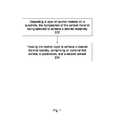
- FIG. 1illustrates an exemplary process to fabricate a thin film cermet resistor according to an embodiment of the present invention.
- Operation 202deposits a layer of cermet material on a substrate with the composition of the cermet material selected to achieve a desired resistivity.
- the cermet layeris deposited by sputtering deposition, for example, by a dc magnetron.
- the sputter depositioncan be performed in reduced pressure (e.g., vacuum or low pressure of mTorr or less), using argon.
- the deposition temperaturecan be less than 400 C, and preferably between 250 and 350 C.
- An optional RF biascan be applied during the sputter deposition, for example, to improve the cermet film quality.
- operation 204treats the deposited cermet layer to achieve a desired thermal stability with the treatment comprising an anneal sequence comprising an optional first anneal, a passivation and a second anneal.
- the anneal processesare performed at high temperature, such as between 400 to 450 C, and preferably higher than 300 C.
- the anneal processesare also performed for a short time, for example, in 5 minutes of less, and preferably between 1 to 2 minutes.
- the anneal processesare also performed in reduced pressure, such as in vacuum ambient.
- the first annealcan performed in-situ with the deposition process, for example, by performing a sequence of deposition/anneal without breaking vacuum or exposing the deposited film to atmospheric ambient.
- the first anneal processcan be performed in the same chamber as the deposition process, after completing the deposition.
- the substratecan be transferred from the deposition chamber to an anneal chamber without exposing to atmospheric ambient, for example, transferred in a cluster tool.
- the first annealcan be optional, for example, by embedding the anneal process with the deposition process.
- the deposition processcan be tailored so that the deposited film can undergo annealing at the same time.
- the passivation processcan be performed at lower temperature and longer time than the anneal processes.
- the passivationis performed at room temperature or at any temperature less than 100 C.
- the passivation timecan be less than 48 hours, and preferably between 3 and 24 hours.
- the passivationcan be performed in oxygen- and/or nitrogen-containing ambient, such as atmospheric ambient.
- the passivationcan be performed in atmospheric pressure, in reduced pressure or in pressure higher than atmospheric pressure.
- accelerate passivationcan be performed to reduce the process time, for example, to be less than 12 hours. For example, higher pressure can be used to accelerate the passivation process.
- the present inventiondiscloses process conditions for film formation with desired resistance and TCR values, comprising an anneal sequence of first anneal, passivation, and second anneal.
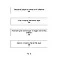
- FIG. 2illustrates an exemplary process for fabricating a thin cermet film according to an embodiment of the present invention.
- Operation 22deposits a cermet layer on a substrate, for example, by a sputtering process.
- Operation 24anneals the deposited cermet layer a first time, such as in vacuum for less than 2 minutes at temperature less than 450 C.
- Operation 26passivates the annealed cermet layer in oxygen-containing ambient at low temperature, such as in air at room temperature and atmospheric pressure for less than 24 hours.
- Operation 28annealed the passivated cermet layer for a second time.
- the conditions for the anneal and the passivation processescan vary from the above described conditions, in order to achieve a thermal stable thin cermet layer, characterized by minimum changes in resistance as function of time or temperature.
- the anneal sequenceis repeated until reaching a desired thermal stability.
- the anneal sequencecan be repeated to reduce the passivation time.
- FIG. 3illustrates a repeated sequence of a cermet layer according to an embodiment of the present invention. After depositing a layer of cermet on a substrate (operation 32 ) with an optional first anneal process (operation 34 ), the cermet layer is then passivated (operation 36 ) and annealed a second time (operation 38 ). The passivation and second anneal is repeated (operation 39 ) until the process is completed, for example, by reaching a desired thermal stability or by saturating the anneal sequence.
- the present inventiondiscloses process conditions for film formation with high resistance and low TCR.
- the present inventiondiscloses a method containing a sequence of process steps that are used to adjust the resistor film properties to achieve thermally stable thin film resistors with targeted resistance and TCR values.
- the resistor filmcomprises cermet materials comprising metal particles embedded in a ceramic matrix, such as dielectric or semiconductor matrix.
- the cermet materialscomprise chromium-silicon compounds, such as Cr—Si—O, CrSi 2 —Cr—SiC, and Si—SiC—CrB 2 .
- cermet resistorsare based on mixture of oxide, boride, or carbide materials.
- the metallic elements usedare chromium, nickel, molybdenum, and cobalt.
- thin filmsare deposited on thermally oxidized silicon wafers using a dc magnetron.
- the filmsare exposed to an elevated temperature, such as less than 450° C., or between 250 to 350° C., with an applied RF bias to the substrate.
- an elevated temperaturesuch as less than 450° C., or between 250 to 350° C.
- a degas step or a pre-heat stepcan be utilized to improve film properties and to improve the repeatability of the process, among other potential benefits.
- the filmsare exposed to an annealing sequence to produce a thermally stable thin film resistor with the targeted TCR and resistance values.
- FIG. 4illustrates an exemplary process of fabricating a thin resistor film according to an embodiment of the present invention.
- the illustrated processcomprises an optimized dc sputter process consisting of a substrate degas step, a sputter deposition step at a temperature 350° C., a dc power level of 300 W, an rf bias power of 50 W, and a double anneal in vacuum at a temperature of 450° C. with an intermediate exposure to atmosphere for preferably 3-24 hours, produces 2.5-4 nm thick CrSi 2 —Cr—SiC cermet films with resistances ranging from 1800 to 1200 ⁇ / ⁇ and TCRs from ⁇ 50 to ⁇ 0 ppm/° C., respectively.
- the exemplary processcomprises an optional degas step 40 , an optional preheat step 41 , a sputter deposition step 42 , a first anneal step 44 , a passivation step 46 , and a second anneal step 48 .
- Degas step 40is commonly implemented prior to a sputter deposition process to remove water vapor, hydrocarbons, and other contaminants from the surface of a wafer that might otherwise have a detrimental effect on the quality of the sputtered film.
- the degas processtypically consists of an exposure to high intensity lamps that provide exposure to heat and light in a vacuum environment that cause the contaminants to desorb from the wafer surface.
- Rf power applied to the substrate in a plasma environmentcan also be used to produce a clean surface prior to sputter deposition step 42 .
- Degas process step 40can be performed in the same chamber within which the sputter process is performed or can be performed in another module or location on the sputter system.
- Preheat step 41is commonly employed to raise the temperature of the wafer for sputter processes that require a substrate to be at elevated temperatures during a subsequent sputter deposition step 42 .
- This stepcan be performed within the same position in which the sputter deposition step is to be performed or elsewhere on the sputter system.
- the sequence of degas and preheat stepscan be in any order (e.g., degas before preheat or preheat before degas) or can be combined together in a single step (e.g., an exposure to high temperature in vacuum ambient that both degas and preheat the substrate at the same time).
- the thin filmsare deposited with an applied rf substrate bias during deposition in the dc magnetron to achieve low TCR values.
- the rf bias poweris typically less than 100 W, and preferably between 30 and 70 W. Films deposited with rf substrate bias generally have lower sheet resistance and higher thermal stability compared to films that are deposited without substrate bias.
- the thin filmsare exposed to a first anneal 44 in vacuum at high temperature, preferably between 400-450° C. for approximately 1-2 minutes.
- This annealis preferably done before exposure of the substrate to ambient conditions and preferably immediately following the sputter deposition, either in the same chamber that was used to deposit the film, or in a second chamber, load lock, or annealing location contained within a clustered arrangement of process and transport modules.
- the anneal processis performed in non-oxygen ambient and at reduced pressure.
- the thin filmsare then exposed to a passivation process 48 , for example, at atmospheric conditions, preferably for 1 to 48 hours and more preferably from 3 to 24 hours.
- the thin filmsare exposed to a second annealing step 48 at high temperature, preferably in vacuum, and preferably between 400-450° C., for 1-2 minutes.
- the anneal treatmentcan change the crystal structure of the deposited thin films, with the adsorbed foreign elements removed, thus stabilizing the cermet film structure.
- Anneal in non-oxidation ambientcan decrease the resistivity of the cermet film using high temperature.
- Anneal in oxygen ambientcan increase the resistivity of the cermet film due to oxidation, such as oxidization of the metal film elements.
- the oxidation effectcan be small.
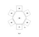
- the sputter deposition process 42can be performed in a sputter deposition module such as the S-Gun magnetron 100 shown in FIG. 5 .
- the S-Gunhas two independently controlled conical targets 114 , 116 mounted concentrically with a central anode 112 .
- Each target 114 , 116is powered by a dc power supply 122 , 124 . Power distribution between the inner and the outer targets enables deposition of highly uniform films onto stationary substrates.
- An additional rf power 126may be applied to the wafer holder 106 , igniting an rf plasma discharge in the wafer vicinity, which generates a negative self-bias potential on the substrate thus creating low energy ion bombardment during the film growth.
- the substrateBefore, during, and/or after deposition, the substrate may be heated to temperatures of up to 500° C. by infrared radiant heater 102 in the S-Gun process module.
- Sputter gastypically argon or a mixture of argon and a reactive gas such as oxygen or nitrogen, if required
- Base vacuum in the process module pumped by turbomolecular pumps and cryopumpsis typically in the range of 1 ⁇ 10 ⁇ 8 to 5 ⁇ 10 ⁇ 7 Torr.
- degas step 40consists of a substrate heating step in the range of 300-500° C. in vacuum for typical times of between 30 to 120 seconds, and preferably at 450° C. for 60 seconds.
- an optional preheat step 41is performed in the preferred embodiment in the same module as subsequent sputter deposition step 42 .
- Preheat step 41is typically implemented to raise the temperature of the wafer so that the temperature of the substrate prior to starting the plasma discharge to enable sputter deposition step 42 is in the range of 300-400° C. and preferably at 350° C.
- the poweris applied to the sputter targets to initiate the discharge and proceed with the sputter deposition onto the substrate.
- the substrateis biased by applying a power source to the substrate or to the substrate support to provide ion bombardment during the deposition process step 42 .
- the first anneal 43is done under vacuum immediately following sputter deposition step 42 .
- the anneal stepcan be done in the same module as the sputter deposition step or in a separate module or position within the cluster module 150 .
- the temperature of the waferreaches 400-500° C. for 1-5 minutes and preferably 450° C. for 1-2 minutes.
- passivation step 44consisting of an exposure to an environment containing oxygen and nitrogen as a precursor to final anneal step 45 , to produce resistive properties in the thin sputter deposited cermet films that are thermally stable.
- passivation process 44is an exposure to air at ambient atmospheric conditions for 3-48 hours and preferably for 24 hours.
- Other embodimentsinclude exposure to air within a module on the vacuum chamber or exposure to oxygen, nitrogen, a gas mixture of nitrogen and oxygen, or a gas mixture that contains oxygen and nitrogen and other gases, the net result of which produces the same effective stabilization of the resistive film properties as is produced upon exposure to air at atmospheric conditions.
- oxygen containing gasessuch as NO 2 , NO, CO, CO 2 , ozone, H 2 O vapor, and others
- inert gasessuch as argon, helium, neon, xenon, or other inert gases, can also be added.
- gases that do not deleteriously affect the process of producing thermally stable resistive filmscan be added to the gas mixture.
- a second anneal step 45follows passivation 44 .
- second anneal 45is performed under vacuum.
- the second anneal step 45can be done on the same module as the sputter deposition step, in a separate module or position within the cluster module 150 on which sputter deposition step 42 was accomplished, a module not connected to the system used for prior steps, or any other system or combination of systems that are necessary to raise the temperature of the substrate to the required anneal temperature to produce thermal stability of the resistive properties of the sputter deposited films.
- typical substrate temperaturesare in the range of 400-500° C. for 1-5 minutes and preferably 450° C. for 1-2 minutes.
- the actual anneal temperaturecan vary depending on factors such as the starting film composition and ultimate target for the TCR. Changes to the anneal temperature and anneal time can be made that produce the same result of thermally stable resistive film properties using the inventive process sequence and would remain within the spirit of the invention. Additionally, the second anneal step could be split into multiple steps to produce similar results of thermally stable resistive film properties from sputter deposited Si x Cr y films.
- Control Si x Cr y films deposited at ambient temperature using sputter deposition step 42results in non-uniform sheet resistance across the substrate upon which the sputtered films are deposited.
- the resistance of these sputtered filmswill gradually increase upon exposure to air at ambient conditions and these sputter deposited films have been found to exhibit changes in resistance when cycled through temperatures in the range of 20 to 120° C.
- Observations of irreversible variation in the measured resistances, as shown in FIG. 7indicates that deposited films are not thermally stable.
- the resistive properties of the filmschange when exposed to temperatures above ambient room temperature (20-30° C.) and that these changes in resistive properties do not return to the original state when the temperatures are returned to ambient.
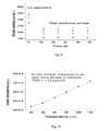
- FIG. 7shows that for an initial sheet resistance of 553.5 ohms/ ⁇ , an increase to a sheet resistance of 555.5 ohms/ ⁇ is observed after cycling the wafer from 20 C to 120° C. and then back to 20° C.
- FIG. 8shows the time dependent resistance of the sputter deposited films upon atmospheric ambient exposure, which illustrates the lack of thermal stability of the sputter depositing Si x Cr y films without the present anneal sequence.
- the sheet resistanceis shown to increase over time for Si x Cr y films deposited at 350° C. for durations up to 50 hours. These data show that deposition at 350° C. is not sufficient to produce Si x Cr y films with thermally stable film properties.
- the average sheet resistance for the films used to collect the data shown in FIG. 8was found to be approximately the same as the films deposited at ambient temperature but the standard deviation for these films deposited at 350° C. was found to be favorably reduced from ⁇ 3% to ⁇ 1%.
- the non-uniformity of the film sheet resistance across the wafer for these testswas measured with an automatic four-point probe.
- the inventive processprovides a method for producing thermal stability in the resistive properties of the Si x Cr y films and reducing or eliminating the variation in film properties observed upon temperature cycling of the thin Si x Cr y films.
- FIG. 9shows the time dependent resistance of the deposited cermet films including the post deposition treatments upon atmospheric ambient exposure, which shows the thermally stable Si x Cr y films.
- the Si x Cr y filmswere fabricated as follows:
- Second anneal step 45450° C. for 120 sec in vacuum
- the sheet resistance measurements from films that were fabricated with and without the post deposition steps 43 , 44 , and 45show that the resistive film properties remain stable for the 50 hour duration of the testing.
- the sheet resistance values for the as-deposited filmsare shown for comparison.
- the addition of post deposition annealing steps 43 , 44 , and 45 in the preferred embodimentensures stabilization of the film resistance which did not change during further storage.
- FIG. 9illustrates an improvement of deposited films after treated with an anneal sequence.
- the observed changes in sheet resistance between the as-deposited films and the films after post deposition steps 43 , 44 , and 45were found to vary with film thickness, but all films exhibited improved thermally stable resistive film properties. It is believed that further optimizations can bring additional improvements to the thermal stability properties.
- TCRthin films with low TCR values
- Metal contactswere deposited over the sputter deposited Si x Cr y films to produce structures for determining the film resistance.
- the TCRwas determined by taking measurements of the resistance using a multimeter at various substrate temperatures from 20° C. to 120° C.
- T 020° C.
- R 0the resistance measured at 20° C.
- T120° C.
- Ris the resistance at 120° C.
- FIG. 10illustrates the resistance measured as a function of temperatures where TCR is calculated to be 14 ppm/° C.
- the resistors or the method of forming the resistors by this inventionare not limited to a reactive sputtering method, but other conventional methods such as chemical vapor deposition (CVD) method, a reactive evaporation method utilizing an electron beam and a plasma ion reactive sputtering method are also applicable.
- the resistor materialsare not limited to cermet materials, but can be applicable for other resistive materials.
- the method by this inventionis not limited to ICs but applicable to other discrete resistors such as a resistor network formed on a ceramic substrate and a discrete film resistor for hybrid circuits.
Landscapes
- Engineering & Computer Science (AREA)
- Microelectronics & Electronic Packaging (AREA)
- Manufacturing & Machinery (AREA)
- Physics & Mathematics (AREA)
- Electromagnetism (AREA)
- Apparatuses And Processes For Manufacturing Resistors (AREA)
- Physical Vapour Deposition (AREA)
Abstract
Description
Claims (20)
Priority Applications (1)
| Application Number | Priority Date | Filing Date | Title |
|---|---|---|---|
| US12/786,238US8482375B2 (en) | 2009-05-24 | 2010-05-24 | Sputter deposition of cermet resistor films with low temperature coefficient of resistance |
Applications Claiming Priority (2)
| Application Number | Priority Date | Filing Date | Title |
|---|---|---|---|
| US18088409P | 2009-05-24 | 2009-05-24 | |
| US12/786,238US8482375B2 (en) | 2009-05-24 | 2010-05-24 | Sputter deposition of cermet resistor films with low temperature coefficient of resistance |
Publications (2)
| Publication Number | Publication Date |
|---|---|
| US20100301989A1 US20100301989A1 (en) | 2010-12-02 |
| US8482375B2true US8482375B2 (en) | 2013-07-09 |
Family
ID=48742831
Family Applications (1)
| Application Number | Title | Priority Date | Filing Date |
|---|---|---|---|
| US12/786,238Active2031-02-19US8482375B2 (en) | 2009-05-24 | 2010-05-24 | Sputter deposition of cermet resistor films with low temperature coefficient of resistance |
Country Status (1)
| Country | Link |
|---|---|
| US (1) | US8482375B2 (en) |
Cited By (1)
| Publication number | Priority date | Publication date | Assignee | Title |
|---|---|---|---|---|
| US20190071767A1 (en)* | 2016-05-16 | 2019-03-07 | Ulvac, Inc. | Method of forming internal stress control film |
Families Citing this family (4)
| Publication number | Priority date | Publication date | Assignee | Title |
|---|---|---|---|---|
| US9963777B2 (en)* | 2012-10-08 | 2018-05-08 | Analog Devices, Inc. | Methods of forming a thin film resistor |
| US20150206798A1 (en)* | 2014-01-17 | 2015-07-23 | Taiwan Semiconductor Manufacturing Company, Ltd. | Interconnect Structure And Method of Forming |
| DE102017114228B4 (en)* | 2017-06-27 | 2021-05-20 | Tdk Electronics Ag | Sheet resistor and thin film sensor |
| CN110132445B (en)* | 2019-04-02 | 2020-10-13 | 上海交通大学 | Negative temperature coefficient resistance type deep low temperature sensor and preparation method thereof |
Citations (77)
| Publication number | Priority date | Publication date | Assignee | Title |
|---|---|---|---|---|
| US3650940A (en) | 1968-02-24 | 1972-03-21 | Siemens Ag | Device for limiting the power supply upon short-circuit between workpiece and tool in electrolytic metal forming machine |
| US3856647A (en) | 1973-05-15 | 1974-12-24 | Ibm | Multi-layer control or stress in thin films |
| US3879278A (en)* | 1970-07-06 | 1975-04-22 | Airco Inc | Composite cermet thin films |
| US4007063A (en) | 1974-08-21 | 1977-02-08 | Toshitaka Yasuda | Heat treating method for metal film resistor |
| US4010312A (en) | 1975-01-23 | 1977-03-01 | Rca Corporation | High resistance cermet film and method of making the same |
| EP0010971A2 (en) | 1978-11-02 | 1980-05-14 | Ford Motor Company Limited | Deposition process |
| US4298804A (en) | 1978-10-13 | 1981-11-03 | U.S. Philips Corporation | Neutron generator having a target |
| GB2106714A (en) | 1981-09-25 | 1983-04-13 | Avx Corp | Ceramic capacitor and method of making the same |
| US4404077A (en) | 1981-04-07 | 1983-09-13 | Fournier Paul R | Integrated sputtering apparatus and method |
| US4427524A (en) | 1982-05-21 | 1984-01-24 | U.S. Philips Corporation | Magnetron cathode sputtering system |
| US4486287A (en) | 1984-02-06 | 1984-12-04 | Fournier Paul R | Cross-field diode sputtering target assembly |
| US4547279A (en) | 1982-10-22 | 1985-10-15 | Hitachi, Ltd. | Sputtering apparatus |
| US4572776A (en) | 1983-12-05 | 1986-02-25 | Leybold-Heraeus Gmbh | Magnetron cathode for sputtering ferromagnetic targets |
| US4595482A (en) | 1984-05-17 | 1986-06-17 | Varian Associates, Inc. | Apparatus for and the method of controlling magnetron sputter device having separate confining magnetic fields to separate targets subject to separate discharges |
| US4619865A (en) | 1984-07-02 | 1986-10-28 | Energy Conversion Devices, Inc. | Multilayer coating and method |
| US4661228A (en) | 1984-05-17 | 1987-04-28 | Varian Associates, Inc. | Apparatus and method for manufacturing planarized aluminum films |
| EP0227438A2 (en) | 1985-12-19 | 1987-07-01 | Varian Associates, Inc. | Magnetron sputter device having separate confining magnetic fields to separate targets and magnetically enhanced R.F. bias |
| JPS63317671A (en) | 1987-06-19 | 1988-12-26 | Shinku Kikai Kogyo Kk | Method and device for sputtering |
| JPH01116068A (en) | 1987-10-28 | 1989-05-09 | Hitachi Ltd | bias sputtering equipment |
| EP0334564A2 (en) | 1988-03-21 | 1989-09-27 | Eaton Corporation | Penning type cathode for sputter coating |
| US4923584A (en) | 1988-10-31 | 1990-05-08 | Eaton Corporation | Sealing apparatus for a vacuum processing system |
| US4946546A (en) | 1987-12-23 | 1990-08-07 | U.S. Philips Corporation | Method of metallizing a substrate of silica, quartz, glass or sapphire |
| US4946576A (en) | 1985-06-12 | 1990-08-07 | Leybold Aktiengesellschaft | Apparatus for the application of thin layers to a substrate |
| JPH02225662A (en) | 1989-02-27 | 1990-09-07 | Tokuda Seisakusho Ltd | sputtering equipment |
| US5096536A (en) | 1990-06-12 | 1992-03-17 | Micron Technology, Inc. | Method and apparatus useful in the plasma etching of semiconductor materials |
| DE4127262C1 (en) | 1991-08-17 | 1992-06-04 | Forschungsges Elektronenstrahl | Sputtering equipment for coating large substrates with (non)ferromagnetic material - consisting of two sub-targets electrically isolated and cooling plates whose gap in between is that in region of pole units |
| US5133850A (en) | 1990-12-31 | 1992-07-28 | Leybold Aktiengesellschaft | Sputtering cathode for coating substrates in cathode sputtering apparatus |
| US5174880A (en) | 1991-08-05 | 1992-12-29 | Hmt Technology Corporation | Magnetron sputter gun target assembly with distributed magnetic field |
| US5266178A (en) | 1991-10-31 | 1993-11-30 | Leybold Aktiengesellschaft | Sputtering cathode |
| US5345534A (en) | 1993-03-29 | 1994-09-06 | Texas Instruments Incorporated | Semiconductor wafer heater with infrared lamp module with light blocking means |
| US5415757A (en) | 1991-11-26 | 1995-05-16 | Leybold Aktiengesellschaft | Apparatus for coating a substrate with electrically nonconductive coatings |
| US5507930A (en) | 1992-03-20 | 1996-04-16 | Komag, Incorporated | Method of sputtering a carbon protective film on a magnetic disk by superimposing an AC voltage on a DC bias voltage |
| US5558749A (en) | 1994-07-08 | 1996-09-24 | Matsushita Electric Industrial Co., Ltd. | Magnetron sputtering apparatus and method |
| US5597459A (en) | 1995-02-08 | 1997-01-28 | Nobler Technologies, Inc. | Magnetron cathode sputtering method and apparatus |
| US5879519A (en) | 1988-02-08 | 1999-03-09 | Optical Coating Laboratory, Inc. | Geometries and configurations for magnetron sputtering apparatus |
| US5882399A (en) | 1997-08-23 | 1999-03-16 | Applied Materials, Inc. | Method of forming a barrier layer which enables a consistently highly oriented crystalline structure in a metallic interconnect |
| US5897753A (en) | 1997-05-28 | 1999-04-27 | Advanced Energy Industries, Inc. | Continuous deposition of insulating material using multiple anodes alternated between positive and negative voltages |
| US5925225A (en) | 1997-03-27 | 1999-07-20 | Applied Materials, Inc. | Method of producing smooth titanium nitride films having low resistivity |
| RU2135634C1 (en) | 1998-06-15 | 1999-08-27 | Санкт-Петербургский государственный технический университет | Method and device for magnetron sputtering |
| JPH11307479A (en) | 1998-04-24 | 1999-11-05 | Anelva Corp | High temperature reflow sputtering method and high temperature reflow sputtering apparatus |
| US6081014A (en) | 1998-11-06 | 2000-06-27 | National Semiconductor Corporation | Silicon carbide chrome thin-film resistor |
| US6130170A (en) | 1997-10-30 | 2000-10-10 | International Business Machines Corporation | Process improvements for titanium-tungsten etching in the presence of electroplated C4's |
| EP1046727A2 (en) | 1999-04-23 | 2000-10-25 | Nippon Sheet Glass Co. Ltd. | Method of film deposition on substrate surface and substrate produced by the method |
| US6154119A (en)* | 1998-06-29 | 2000-11-28 | The Regents Of The University Of California | TI--CR--AL--O thin film resistors |
| US6171922B1 (en) | 1993-09-01 | 2001-01-09 | National Semiconductor Corporation | SiCr thin film resistors having improved temperature coefficients of resistance and sheet resistance |
| WO2001029278A1 (en) | 1999-10-15 | 2001-04-26 | Advanced Energy Industries, Inc. | Method and apparatus for substrate biasing in multiple electrode sputtering systems |
| US6294444B1 (en) | 1998-07-21 | 2001-09-25 | Fuji Electric Co., Ltd. | Method for manufacturing silicon carbide semiconductor device |
| WO2001084619A2 (en) | 2000-05-04 | 2001-11-08 | Applied Materials, Inc. | Method of depositing low stress films |
| US6342448B1 (en) | 2000-05-31 | 2002-01-29 | Taiwan Semiconductor Manufacturing Company | Method of fabricating barrier adhesion to low-k dielectric layers in a copper damascene process |
| JP2002033325A (en) | 2000-07-13 | 2002-01-31 | Shin Etsu Handotai Co Ltd | Silicon wafer manufacturing method |
| US6352627B2 (en) | 1997-04-14 | 2002-03-05 | Cemecon-Ceramic Metal Coatings | Method and device for PVD coating |
| US6375810B2 (en) | 1997-08-07 | 2002-04-23 | Applied Materials, Inc. | Plasma vapor deposition with coil sputtering |
| US6399411B1 (en) | 1996-12-17 | 2002-06-04 | Canon Kabushiki Kaisha | Method for forming non-single-crystal semiconductor thin film, and method for producing photovoltaic device |
| US20020075131A1 (en) | 2000-05-18 | 2002-06-20 | Coates Karen L. | Cermet thin film resistors |
| US6420863B1 (en) | 1998-10-22 | 2002-07-16 | Fraunhofer-Gesellschaft zur Förderung der angewandten Forschung e.V | Method for monitoring alternating current discharge on a double electrode and apparatus |
| US20020093101A1 (en) | 2000-06-22 | 2002-07-18 | Subramoney Iyer | Method of metallization using a nickel-vanadium layer |
| US6482681B1 (en) | 2000-05-05 | 2002-11-19 | International Rectifier Corporation | Hydrogen implant for buffer zone of punch-through non epi IGBT |
| US6488823B1 (en) | 1997-05-27 | 2002-12-03 | Applied Materials, Inc. | Stress tunable tantalum and tantalum nitride films |
| US20030017628A1 (en) | 2001-07-18 | 2003-01-23 | Applied Materials, Inc. | Monitoring process for oxide removal |
| US20030068898A1 (en) | 2001-10-10 | 2003-04-10 | Chun-Hung Lee | Dry etching method for manufacturing processes of semiconductor devices |
| US20030109198A1 (en) | 2000-08-30 | 2003-06-12 | Whonchee Lee | Methods and apparatus for electrically detecting characteristics of a microelectronic substrate and/or polishing medium |
| US20030132524A1 (en) | 2002-01-16 | 2003-07-17 | Felmetsger Valery V. | Permanent adherence of the back end of a wafer to an electrical component or sub-assembly |
| US20030205460A1 (en) | 2002-04-12 | 2003-11-06 | Buda Paul R. | Apparatus and method for arc detection |
| US6720261B1 (en) | 1999-06-02 | 2004-04-13 | Agere Systems Inc. | Method and system for eliminating extrusions in semiconductor vias |
| US20040163952A1 (en) | 2003-02-21 | 2004-08-26 | Yury Oshmyansky | Magnetron with adjustable target positioning |
| US20040168637A1 (en) | 2000-04-10 | 2004-09-02 | Gorokhovsky Vladimir I. | Filtered cathodic arc deposition method and apparatus |
| US6806173B1 (en) | 1999-02-26 | 2004-10-19 | Robert Bosch Gmbh | Method for producing highly doped semiconductor components |
| US20040231972A1 (en) | 2003-05-23 | 2004-11-25 | Laptev Pavel N. | Reactive sputtering of silicon nitride films by RF supported DC magnetron |
| US6824653B2 (en) | 2003-02-21 | 2004-11-30 | Agilent Technologies, Inc | Magnetron with controlled DC power |
| US20040253828A1 (en) | 2003-06-16 | 2004-12-16 | Takeshi Ozawa | Fabrication method of semiconductor integrated circuit device |
| US6863987B2 (en) | 2000-02-23 | 2005-03-08 | Nippon Steel Corporation | Titanium resistant to discoloration in atmospheric environment and process of production of same |
| US20070046927A1 (en) | 2005-08-31 | 2007-03-01 | Applied Materials, Inc. | Integrated metrology tools for monitoring and controlling large area substrate processing chambers |
| US20070080611A1 (en) | 2005-10-12 | 2007-04-12 | Ube Industries, Ltd. | Aluminum nitride thin film, composite film containing the same and piezoelectric thin film resonator using the same |
| US20070235810A1 (en) | 2006-04-07 | 2007-10-11 | Delgado Eladio C | Power semiconductor module and fabrication method |
| US20080083611A1 (en) | 2006-10-06 | 2008-04-10 | Tegal Corporation | High-adhesive backside metallization |
| US20090246385A1 (en) | 2008-03-25 | 2009-10-01 | Tegal Corporation | Control of crystal orientation and stress in sputter deposited thin films |
| US20090242392A1 (en) | 2008-03-25 | 2009-10-01 | Tegal Corporation | Stress adjustment in reactive sputtering |
Family Cites Families (1)
| Publication number | Priority date | Publication date | Assignee | Title |
|---|---|---|---|---|
| US6120261A (en)* | 1998-08-25 | 2000-09-19 | Saudi Arabian Oil Company | Electric submersible pump with hollow drive shaft |
- 2010
- 2010-05-24USUS12/786,238patent/US8482375B2/enactiveActive
Patent Citations (82)
| Publication number | Priority date | Publication date | Assignee | Title |
|---|---|---|---|---|
| US3650940A (en) | 1968-02-24 | 1972-03-21 | Siemens Ag | Device for limiting the power supply upon short-circuit between workpiece and tool in electrolytic metal forming machine |
| US3879278A (en)* | 1970-07-06 | 1975-04-22 | Airco Inc | Composite cermet thin films |
| US3856647A (en) | 1973-05-15 | 1974-12-24 | Ibm | Multi-layer control or stress in thin films |
| US4007063A (en) | 1974-08-21 | 1977-02-08 | Toshitaka Yasuda | Heat treating method for metal film resistor |
| US4010312A (en) | 1975-01-23 | 1977-03-01 | Rca Corporation | High resistance cermet film and method of making the same |
| US4298804A (en) | 1978-10-13 | 1981-11-03 | U.S. Philips Corporation | Neutron generator having a target |
| EP0010971A2 (en) | 1978-11-02 | 1980-05-14 | Ford Motor Company Limited | Deposition process |
| US4404077A (en) | 1981-04-07 | 1983-09-13 | Fournier Paul R | Integrated sputtering apparatus and method |
| GB2106714A (en) | 1981-09-25 | 1983-04-13 | Avx Corp | Ceramic capacitor and method of making the same |
| US4427524A (en) | 1982-05-21 | 1984-01-24 | U.S. Philips Corporation | Magnetron cathode sputtering system |
| US4547279A (en) | 1982-10-22 | 1985-10-15 | Hitachi, Ltd. | Sputtering apparatus |
| US4572776A (en) | 1983-12-05 | 1986-02-25 | Leybold-Heraeus Gmbh | Magnetron cathode for sputtering ferromagnetic targets |
| US4486287A (en) | 1984-02-06 | 1984-12-04 | Fournier Paul R | Cross-field diode sputtering target assembly |
| US4595482A (en) | 1984-05-17 | 1986-06-17 | Varian Associates, Inc. | Apparatus for and the method of controlling magnetron sputter device having separate confining magnetic fields to separate targets subject to separate discharges |
| US4661228A (en) | 1984-05-17 | 1987-04-28 | Varian Associates, Inc. | Apparatus and method for manufacturing planarized aluminum films |
| US4619865A (en) | 1984-07-02 | 1986-10-28 | Energy Conversion Devices, Inc. | Multilayer coating and method |
| US4946576A (en) | 1985-06-12 | 1990-08-07 | Leybold Aktiengesellschaft | Apparatus for the application of thin layers to a substrate |
| EP0227438A2 (en) | 1985-12-19 | 1987-07-01 | Varian Associates, Inc. | Magnetron sputter device having separate confining magnetic fields to separate targets and magnetically enhanced R.F. bias |
| JPS63317671A (en) | 1987-06-19 | 1988-12-26 | Shinku Kikai Kogyo Kk | Method and device for sputtering |
| JPH01116068A (en) | 1987-10-28 | 1989-05-09 | Hitachi Ltd | bias sputtering equipment |
| US4946546A (en) | 1987-12-23 | 1990-08-07 | U.S. Philips Corporation | Method of metallizing a substrate of silica, quartz, glass or sapphire |
| US5879519A (en) | 1988-02-08 | 1999-03-09 | Optical Coating Laboratory, Inc. | Geometries and configurations for magnetron sputtering apparatus |
| EP0334564A2 (en) | 1988-03-21 | 1989-09-27 | Eaton Corporation | Penning type cathode for sputter coating |
| US4923584A (en) | 1988-10-31 | 1990-05-08 | Eaton Corporation | Sealing apparatus for a vacuum processing system |
| JPH02225662A (en) | 1989-02-27 | 1990-09-07 | Tokuda Seisakusho Ltd | sputtering equipment |
| US5096536A (en) | 1990-06-12 | 1992-03-17 | Micron Technology, Inc. | Method and apparatus useful in the plasma etching of semiconductor materials |
| US5133850A (en) | 1990-12-31 | 1992-07-28 | Leybold Aktiengesellschaft | Sputtering cathode for coating substrates in cathode sputtering apparatus |
| US5174880A (en) | 1991-08-05 | 1992-12-29 | Hmt Technology Corporation | Magnetron sputter gun target assembly with distributed magnetic field |
| DE4127262C1 (en) | 1991-08-17 | 1992-06-04 | Forschungsges Elektronenstrahl | Sputtering equipment for coating large substrates with (non)ferromagnetic material - consisting of two sub-targets electrically isolated and cooling plates whose gap in between is that in region of pole units |
| US5266178A (en) | 1991-10-31 | 1993-11-30 | Leybold Aktiengesellschaft | Sputtering cathode |
| US5415757A (en) | 1991-11-26 | 1995-05-16 | Leybold Aktiengesellschaft | Apparatus for coating a substrate with electrically nonconductive coatings |
| US5507930A (en) | 1992-03-20 | 1996-04-16 | Komag, Incorporated | Method of sputtering a carbon protective film on a magnetic disk by superimposing an AC voltage on a DC bias voltage |
| US5345534A (en) | 1993-03-29 | 1994-09-06 | Texas Instruments Incorporated | Semiconductor wafer heater with infrared lamp module with light blocking means |
| US6171922B1 (en) | 1993-09-01 | 2001-01-09 | National Semiconductor Corporation | SiCr thin film resistors having improved temperature coefficients of resistance and sheet resistance |
| US5558749A (en) | 1994-07-08 | 1996-09-24 | Matsushita Electric Industrial Co., Ltd. | Magnetron sputtering apparatus and method |
| US5597459A (en) | 1995-02-08 | 1997-01-28 | Nobler Technologies, Inc. | Magnetron cathode sputtering method and apparatus |
| US6399411B1 (en) | 1996-12-17 | 2002-06-04 | Canon Kabushiki Kaisha | Method for forming non-single-crystal semiconductor thin film, and method for producing photovoltaic device |
| US5925225A (en) | 1997-03-27 | 1999-07-20 | Applied Materials, Inc. | Method of producing smooth titanium nitride films having low resistivity |
| US6352627B2 (en) | 1997-04-14 | 2002-03-05 | Cemecon-Ceramic Metal Coatings | Method and device for PVD coating |
| US6488823B1 (en) | 1997-05-27 | 2002-12-03 | Applied Materials, Inc. | Stress tunable tantalum and tantalum nitride films |
| US5897753A (en) | 1997-05-28 | 1999-04-27 | Advanced Energy Industries, Inc. | Continuous deposition of insulating material using multiple anodes alternated between positive and negative voltages |
| US6375810B2 (en) | 1997-08-07 | 2002-04-23 | Applied Materials, Inc. | Plasma vapor deposition with coil sputtering |
| US5882399A (en) | 1997-08-23 | 1999-03-16 | Applied Materials, Inc. | Method of forming a barrier layer which enables a consistently highly oriented crystalline structure in a metallic interconnect |
| US6130170A (en) | 1997-10-30 | 2000-10-10 | International Business Machines Corporation | Process improvements for titanium-tungsten etching in the presence of electroplated C4's |
| JPH11307479A (en) | 1998-04-24 | 1999-11-05 | Anelva Corp | High temperature reflow sputtering method and high temperature reflow sputtering apparatus |
| RU2135634C1 (en) | 1998-06-15 | 1999-08-27 | Санкт-Петербургский государственный технический университет | Method and device for magnetron sputtering |
| US6154119A (en)* | 1998-06-29 | 2000-11-28 | The Regents Of The University Of California | TI--CR--AL--O thin film resistors |
| US6294444B1 (en) | 1998-07-21 | 2001-09-25 | Fuji Electric Co., Ltd. | Method for manufacturing silicon carbide semiconductor device |
| US6420863B1 (en) | 1998-10-22 | 2002-07-16 | Fraunhofer-Gesellschaft zur Förderung der angewandten Forschung e.V | Method for monitoring alternating current discharge on a double electrode and apparatus |
| US6081014A (en) | 1998-11-06 | 2000-06-27 | National Semiconductor Corporation | Silicon carbide chrome thin-film resistor |
| US6806173B1 (en) | 1999-02-26 | 2004-10-19 | Robert Bosch Gmbh | Method for producing highly doped semiconductor components |
| JP2001003166A (en) | 1999-04-23 | 2001-01-09 | Nippon Sheet Glass Co Ltd | Method for coating surface of substrate with coating film and substrate by using the method |
| EP1046727A2 (en) | 1999-04-23 | 2000-10-25 | Nippon Sheet Glass Co. Ltd. | Method of film deposition on substrate surface and substrate produced by the method |
| US6720261B1 (en) | 1999-06-02 | 2004-04-13 | Agere Systems Inc. | Method and system for eliminating extrusions in semiconductor vias |
| WO2001029278A1 (en) | 1999-10-15 | 2001-04-26 | Advanced Energy Industries, Inc. | Method and apparatus for substrate biasing in multiple electrode sputtering systems |
| US6863987B2 (en) | 2000-02-23 | 2005-03-08 | Nippon Steel Corporation | Titanium resistant to discoloration in atmospheric environment and process of production of same |
| US20040168637A1 (en) | 2000-04-10 | 2004-09-02 | Gorokhovsky Vladimir I. | Filtered cathodic arc deposition method and apparatus |
| WO2001084619A2 (en) | 2000-05-04 | 2001-11-08 | Applied Materials, Inc. | Method of depositing low stress films |
| US6482681B1 (en) | 2000-05-05 | 2002-11-19 | International Rectifier Corporation | Hydrogen implant for buffer zone of punch-through non epi IGBT |
| US20020075131A1 (en) | 2000-05-18 | 2002-06-20 | Coates Karen L. | Cermet thin film resistors |
| US6342448B1 (en) | 2000-05-31 | 2002-01-29 | Taiwan Semiconductor Manufacturing Company | Method of fabricating barrier adhesion to low-k dielectric layers in a copper damascene process |
| US20020093101A1 (en) | 2000-06-22 | 2002-07-18 | Subramoney Iyer | Method of metallization using a nickel-vanadium layer |
| JP2002033325A (en) | 2000-07-13 | 2002-01-31 | Shin Etsu Handotai Co Ltd | Silicon wafer manufacturing method |
| EP1306896A1 (en) | 2000-07-13 | 2003-05-02 | Shin-Etsu Handotai Co., Ltd | Method for manufacturing silicon wafer |
| US20030109198A1 (en) | 2000-08-30 | 2003-06-12 | Whonchee Lee | Methods and apparatus for electrically detecting characteristics of a microelectronic substrate and/or polishing medium |
| US20030017628A1 (en) | 2001-07-18 | 2003-01-23 | Applied Materials, Inc. | Monitoring process for oxide removal |
| US20030068898A1 (en) | 2001-10-10 | 2003-04-10 | Chun-Hung Lee | Dry etching method for manufacturing processes of semiconductor devices |
| US20030132524A1 (en) | 2002-01-16 | 2003-07-17 | Felmetsger Valery V. | Permanent adherence of the back end of a wafer to an electrical component or sub-assembly |
| US20030205460A1 (en) | 2002-04-12 | 2003-11-06 | Buda Paul R. | Apparatus and method for arc detection |
| US20040163952A1 (en) | 2003-02-21 | 2004-08-26 | Yury Oshmyansky | Magnetron with adjustable target positioning |
| US6824653B2 (en) | 2003-02-21 | 2004-11-30 | Agilent Technologies, Inc | Magnetron with controlled DC power |
| US7179350B2 (en) | 2003-05-23 | 2007-02-20 | Tegal Corporation | Reactive sputtering of silicon nitride films by RF supported DC magnetron |
| WO2004107411A2 (en) | 2003-05-23 | 2004-12-09 | Sputtered Films, Inc. | Deposition apparatus and method |
| US20040231972A1 (en) | 2003-05-23 | 2004-11-25 | Laptev Pavel N. | Reactive sputtering of silicon nitride films by RF supported DC magnetron |
| US20040253828A1 (en) | 2003-06-16 | 2004-12-16 | Takeshi Ozawa | Fabrication method of semiconductor integrated circuit device |
| US20070046927A1 (en) | 2005-08-31 | 2007-03-01 | Applied Materials, Inc. | Integrated metrology tools for monitoring and controlling large area substrate processing chambers |
| US20070080611A1 (en) | 2005-10-12 | 2007-04-12 | Ube Industries, Ltd. | Aluminum nitride thin film, composite film containing the same and piezoelectric thin film resonator using the same |
| US20070235810A1 (en) | 2006-04-07 | 2007-10-11 | Delgado Eladio C | Power semiconductor module and fabrication method |
| US20080083611A1 (en) | 2006-10-06 | 2008-04-10 | Tegal Corporation | High-adhesive backside metallization |
| US20090246385A1 (en) | 2008-03-25 | 2009-10-01 | Tegal Corporation | Control of crystal orientation and stress in sputter deposited thin films |
| US20090242392A1 (en) | 2008-03-25 | 2009-10-01 | Tegal Corporation | Stress adjustment in reactive sputtering |
| US20090242388A1 (en) | 2008-03-25 | 2009-10-01 | Tegal Corporation | Stress adjustment in reactive sputtering |
Non-Patent Citations (48)
| Title |
|---|
| Alami et al., "Ion-Assisted Physical Vapor Deposition for Enhanced Film Properties on Nonflat Surfaces", J. Vac. Sci. Technol. A 23(2), Mar./Apr. 2005, 278-280. |
| Beach, "Design of Low-Temperature Thermal Chemical Vapor Deposition Processes", IBM J. REs. Develop., Nov. 1990, vol. 34, No. 6. |
| Blachman, "Stress and Resistivity Control in Sputtered Molybdenum Films and Comparison with Sputtered Gold", Metallurgical Transactions, 2, 1971, 699-709. |
| Chiu et al., "The Control of Film Stress Using Ionised Magnetron Sputter Deposition", Thin Solid Films, 343-344-(1999) 39-42. |
| Dubois et al, "Stress and Piezoelectric Properties of Aluminum Snitide Thin Films Deposited onto Metal Electrodes by Pulsed Direct Current Reactive Sputtering", Journal of Applied Physics, vol. 89, No. 11, 6389-6395. |
| Este et al., "Stress Control in Reactively Sputtered AlN and TiN Films", J. Vac. Sci. Technol. A5 (4), Jul./Aug. 1987, 1892-1897. |
| Felmetsger, "Design, operation mode, and stress control capability of S-Gun magnetron for AC reactive sputtering." Surface & Coating Technology 204 (2009) 840-844, 840-844. |
| Felmetsger, "High-adhesive back side metallization of ultrathin wafers." J. Vac. Sci. Technology B 25(3), May/Jun. 2007, 881-885. |
| Felmetsger, "Stress Control in Multi-Layer Backside Metallization on Thinned Wafers", Oct. 1999, Sputtered Films, Inc., pp. 1-15. |
| Felmetsger, "Tailoring Sputtered Cr Films on Large Wafers", 1999, Sputtered Films, Inc., pp. 1-8. |
| Final Office Action for U.S. Appl. No. 09/949,181 dated Nov. 15, 2002. |
| Final Office Action for U.S. Appl. No. 10/051,886 dated Apr. 20, 2004. |
| Final Office Action for U.S. Appl. No. 10/051,886 dated Jan. 24, 2006. |
| Final Office Action for U.S. Appl. No. 11/863,046 dated Apr. 6, 2012. |
| Final Office Action for U.S. Appl. No. 11/863,046 dated Mar. 10, 2011. |
| Final Office Action for U.S. Appl. No. 12/411,301 dated Apr. 24, 2012. |
| Final Office Action for U.S. Appl. No. 12/411,357 dated Mar. 29, 2012. |
| Final Office Action for U.S. Appl. No. 12/411,369 dated Mar. 14, 2012. |
| International Preliminary Report on Patentability for international application No. PCT/US2007/080237, dated Apr. 7, 2009. |
| Iriarte et al, "Influence of Deposition Parameters on the Stress of Magnetron Sputter-Deposited AlN Thin Films on Si(100) Substrates", J. Mater. Res., vol. 18, No. 2, 2003, 423-432. |
| Ko et al., "Microstructure Analyses of the Titanium Films Formed by the Ionized Sputtering Process", Thin Solid Films 340, (1999), 13-17. |
| Lundqvist N., Aberg J., Nygren S., Bjormander C, Zhang S. Effects fo substrate bias and temperature during titanium sputter-depostion on the phase formation in TiSi2. Microelectronics Engineering 60 (2002) 211-220. |
| Naik et al, "Low Temperature Deposition of Highly Textured AlN Film by Direct Current Magnetron Sputtering for Application in Thin Film Resonators", J. Electrochem. Soc., 146, 691-696, 1999. |
| Non-Final Office Action for U.S. Appl. No. 09/949,181 dated Jan. 27, 2004. |
| Non-Final office Action for U.S. Appl. No. 09/949,181 dated Jul. 24, 2002. |
| Non-Final Office Action for U.S. Appl. No. 09/949,181 dated Mar. 18, 2002. |
| Non-Final Office Action for U.S. Appl. No. 10/051,886 dated Aug. 23, 2005. |
| Non-Final Office Action for U.S. Appl. No. 10/051,886 dated Jun. 29, 2006. |
| Non-Final Office Action for U.S. Appl. No. 10/051,886 dated Mar. 4, 2003. |
| Non-Final Office Action for U.S. Appl. No. 10/051,886 dated Nov. 17, 2004. |
| Non-Final Office Action for U.S. Appl. No. 10/051,886 dated Oct. 20, 2003. |
| Non-Final Office Action for U.S. Appl. No. 10/371,463 dated May 6, 2004. |
| Non-Final Office Action for U.S. Appl. No. 10/446,005 dated Apr. 21, 2006. |
| Non-Final Office Action for U.S. Appl. No. 11/863,046 dated Nov. 4, 2011. |
| Non-Final Office Action for U.S. Appl. No. 11/863,046 dated Oct. 11, 2012. |
| Non-Final Office Action for U.S. Appl. No. 11/863,046 dated Sep. 24, 2010. |
| Non-Final Office Action for U.S. Appl. No. 12/411,301 dated Dec. 11, 2012. |
| Non-Final Office Action for U.S. Appl. No. 12/411,301 dated Oct. 27, 2011. |
| Non-Final Office Action for U.S. Appl. No. 12/411,357 dated Nov. 9, 2011. |
| Non-Final Office Action for U.S. Appl. No. 12/411,357 dated Oct. 4, 2012. |
| Non-Final Office Action for U.S. Appl. No. 12/411,369 dated Jul. 19, 2012. |
| Non-Final Office Action for U.S. Appl. No. 12/411,369 dated Nov. 4, 2011. |
| Non-Final Office Action for U.S. Appl. No. 12/786,238 dated Jul. 24, 2012. |
| Oshmyansky et al, "Sputtering Process for Bulk Acoustic Wave Filters", Semiconductor Int., Mar. 2003. |
| Sricharoenchai P, Panich N, Visuttipitukul P, Wangyao. Effect of Substrate Temperature, Biasing and Sputter Cleaning on the Structure and Properties of Nanostructured TiB2 Coatings on High Speed Steel. Materials Transactions, vol. 51, No. 2 (2010), 246-252. |
| Thornton, "The Microstructure of Sputter-Deposited Coatings", J. Vac. Sci. Technol. A4 (6), Nov./Dec. 1986, 3059-3065. |
| Windischmann, "Intrinsic Stress in Sputter-Deposited Thin Films", Critical Reviews in Solid State and Materials Sciences, 17:6, 547-596., 1992. |
| Winidschmann, "Intrinsic Strerss in Sputtered Thin Films", J. Vac. Sci. Technol. A9 (4), Jul./Aug. 1991, 2431-2436. |
Cited By (2)
| Publication number | Priority date | Publication date | Assignee | Title |
|---|---|---|---|---|
| US20190071767A1 (en)* | 2016-05-16 | 2019-03-07 | Ulvac, Inc. | Method of forming internal stress control film |
| US10975465B2 (en)* | 2016-05-16 | 2021-04-13 | Ulvac, Inc. | Method of forming internal stress control film |
Also Published As
| Publication number | Publication date |
|---|---|
| US20100301989A1 (en) | 2010-12-02 |
Similar Documents
| Publication | Publication Date | Title |
|---|---|---|
| EP0082183B1 (en) | Thin film resistor material and method | |
| US8482375B2 (en) | Sputter deposition of cermet resistor films with low temperature coefficient of resistance | |
| JPH05507115A (en) | Method and structure for forming alpha Ta in thin film form | |
| US4591821A (en) | Chromium-silicon-nitrogen thin film resistor and apparatus | |
| CN103714927B (en) | The method for forming thin film resistor | |
| JP2002517084A (en) | Resistor having low temperature coefficient of resistance and method of manufacturing the same | |
| JPS5955001A (en) | Resistor | |
| US6217722B1 (en) | Process for producing Ti-Cr-Al-O thin film resistors | |
| US5585776A (en) | Thin film resistors comprising ruthenium oxide | |
| TW202316451A (en) | Resistor material, resistor element and method of manufacturing resistor element | |
| Nachrodt et al. | Ti/Ni (80%) Cr (20%) thin-film resistor with a nearly zero temperature coefficient of resistance for integration in a standard CMOS process | |
| KR0161376B1 (en) | Metal wiring forming method and sputtering apparatus used therein | |
| Tong et al. | Temperature dependence of resistance in reactively sputtered RuO~ 2 thin films | |
| JP4380586B2 (en) | Thin film resistor and manufacturing method thereof | |
| Cho et al. | Preparation of Cr–Si multilayer structures for thin film heater applications | |
| US20030183897A1 (en) | Metal oxide temperature monitor | |
| US20090308859A1 (en) | Ceramic heater and method of manufacturing the same | |
| Birkett et al. | Structural and electrical properties of CuAlMo thin films prepared by magnetron sputtering | |
| Nowicki et al. | Comparison of the Properties of Molybdenum Silicide Films Deposited by D‐C Magnetron and RF Diode Co‐Deposition | |
| JPH05175157A (en) | Method for forming titanium compound film | |
| EP2100313B1 (en) | High resistivity thin film composition and fabrication method | |
| US7276777B2 (en) | Thin film resistor and method of making the same | |
| Thiel et al. | TCR control of Ni/Cr resistors | |
| Gottlieb et al. | Temperature dependence of resistivity for TiN and ti-si-N films | |
| JPH06275409A (en) | Method of manufacturing thin film resistance element |
Legal Events
| Date | Code | Title | Description |
|---|---|---|---|
| AS | Assignment | Owner name:OEM GROUP, INC., ARIZONA Free format text:ASSIGNMENT OF ASSIGNORS INTEREST;ASSIGNOR:FELMETSGER, VALERY;REEL/FRAME:024460/0508 Effective date:20100524 | |
| STCF | Information on status: patent grant | Free format text:PATENTED CASE | |
| AS | Assignment | Owner name:OEM GROUP, LLC, ARIZONA Free format text:CHANGE OF NAME;ASSIGNOR:OEM GROUP, INC.;REEL/FRAME:038083/0231 Effective date:20160309 | |
| AS | Assignment | Owner name:THL CORPORATE FINANCE, INC., AS COLLATERAL AGENT, Free format text:SECURITY INTEREST;ASSIGNOR:OEM GROUP, LLC;REEL/FRAME:038355/0078 Effective date:20160316 | |
| FPAY | Fee payment | Year of fee payment:4 | |
| FEPP | Fee payment procedure | Free format text:7.5 YR SURCHARGE - LATE PMT W/IN 6 MO, SMALL ENTITY (ORIGINAL EVENT CODE: M2555); ENTITY STATUS OF PATENT OWNER: SMALL ENTITY | |
| MAFP | Maintenance fee payment | Free format text:PAYMENT OF MAINTENANCE FEE, 8TH YR, SMALL ENTITY (ORIGINAL EVENT CODE: M2552); ENTITY STATUS OF PATENT OWNER: SMALL ENTITY Year of fee payment:8 | |
| MAFP | Maintenance fee payment | Free format text:PAYMENT OF MAINTENANCE FEE, 12TH YR, SMALL ENTITY (ORIGINAL EVENT CODE: M2553); ENTITY STATUS OF PATENT OWNER: SMALL ENTITY Year of fee payment:12 |