US8481385B2 - Methods of fabricating a memory device - Google Patents
Methods of fabricating a memory deviceDownload PDFInfo
- Publication number
- US8481385B2 US8481385B2US13/469,513US201213469513AUS8481385B2US 8481385 B2US8481385 B2US 8481385B2US 201213469513 AUS201213469513 AUS 201213469513AUS 8481385 B2US8481385 B2US 8481385B2
- Authority
- US
- United States
- Prior art keywords
- source
- forming
- memory device
- gate
- drain region
- Prior art date
- Legal status (The legal status is an assumption and is not a legal conclusion. Google has not performed a legal analysis and makes no representation as to the accuracy of the status listed.)
- Expired - Lifetime
Links
Images


Classifications
- H—ELECTRICITY
- H10—SEMICONDUCTOR DEVICES; ELECTRIC SOLID-STATE DEVICES NOT OTHERWISE PROVIDED FOR
- H10D—INORGANIC ELECTRIC SEMICONDUCTOR DEVICES
- H10D84/00—Integrated devices formed in or on semiconductor substrates that comprise only semiconducting layers, e.g. on Si wafers or on GaAs-on-Si wafers
- H10D84/01—Manufacture or treatment
- H10D84/0123—Integrating together multiple components covered by H10D12/00 or H10D30/00, e.g. integrating multiple IGBTs
- H10D84/0126—Integrating together multiple components covered by H10D12/00 or H10D30/00, e.g. integrating multiple IGBTs the components including insulated gates, e.g. IGFETs
- H10D84/016—Integrating together multiple components covered by H10D12/00 or H10D30/00, e.g. integrating multiple IGBTs the components including insulated gates, e.g. IGFETs the components including vertical IGFETs
- H—ELECTRICITY
- H10—SEMICONDUCTOR DEVICES; ELECTRIC SOLID-STATE DEVICES NOT OTHERWISE PROVIDED FOR
- H10B—ELECTRONIC MEMORY DEVICES
- H10B12/00—Dynamic random access memory [DRAM] devices
- H10B12/01—Manufacture or treatment
- H10B12/02—Manufacture or treatment for one transistor one-capacitor [1T-1C] memory cells
- H10B12/05—Making the transistor
- H10B12/053—Making the transistor the transistor being at least partially in a trench in the substrate
- H—ELECTRICITY
- H10—SEMICONDUCTOR DEVICES; ELECTRIC SOLID-STATE DEVICES NOT OTHERWISE PROVIDED FOR
- H10D—INORGANIC ELECTRIC SEMICONDUCTOR DEVICES
- H10D84/00—Integrated devices formed in or on semiconductor substrates that comprise only semiconducting layers, e.g. on Si wafers or on GaAs-on-Si wafers
- H10D84/01—Manufacture or treatment
- H10D84/02—Manufacture or treatment characterised by using material-based technologies
- H10D84/03—Manufacture or treatment characterised by using material-based technologies using Group IV technology, e.g. silicon technology or silicon-carbide [SiC] technology
- H10D84/038—Manufacture or treatment characterised by using material-based technologies using Group IV technology, e.g. silicon technology or silicon-carbide [SiC] technology using silicon technology, e.g. SiGe
- H—ELECTRICITY
- H10—SEMICONDUCTOR DEVICES; ELECTRIC SOLID-STATE DEVICES NOT OTHERWISE PROVIDED FOR
- H10B—ELECTRONIC MEMORY DEVICES
- H10B12/00—Dynamic random access memory [DRAM] devices
- H10B12/30—DRAM devices comprising one-transistor - one-capacitor [1T-1C] memory cells
- H10B12/31—DRAM devices comprising one-transistor - one-capacitor [1T-1C] memory cells having a storage electrode stacked over the transistor
- H10B12/318—DRAM devices comprising one-transistor - one-capacitor [1T-1C] memory cells having a storage electrode stacked over the transistor the storage electrode having multiple segments
- H—ELECTRICITY
- H10—SEMICONDUCTOR DEVICES; ELECTRIC SOLID-STATE DEVICES NOT OTHERWISE PROVIDED FOR
- H10B—ELECTRONIC MEMORY DEVICES
- H10B12/00—Dynamic random access memory [DRAM] devices
- H10B12/30—DRAM devices comprising one-transistor - one-capacitor [1T-1C] memory cells
- H10B12/34—DRAM devices comprising one-transistor - one-capacitor [1T-1C] memory cells the transistor being at least partially in a trench in the substrate
- H—ELECTRICITY
- H10—SEMICONDUCTOR DEVICES; ELECTRIC SOLID-STATE DEVICES NOT OTHERWISE PROVIDED FOR
- H10B—ELECTRONIC MEMORY DEVICES
- H10B12/00—Dynamic random access memory [DRAM] devices
- H10B12/30—DRAM devices comprising one-transistor - one-capacitor [1T-1C] memory cells
- H10B12/48—Data lines or contacts therefor
- H10B12/485—Bit line contacts
Definitions
- This inventionrelates to microelectronic devices and related fabrication methods. More particularly, this invention relates to a memory device having a digit line that is directly coupled to a transistor source.
- DRAMDynamic Random Access Memory
- RAMsemiconductor Random Access Memory
- a DRAM celltypically comprises a charge storage capacitor (or cell capacitor) coupled to an access device, such as a Metal-Oxide-Semiconductor Field Effect Transistor (MOSFET, or simply FET).
- MOSFETMetal-Oxide-Semiconductor Field Effect Transistor
- These access devicesfunctions to apply or remove charge on the capacitor, thus affecting a logical state defined by the stored charge.
- the amount of charge stored on the capacitoris determined by the electrode (or storage node) area and the interelectrode spacing.
- the conditions of DRAM operationsuch as operating voltage, leakage rate and refresh rate, will generally mandate that a certain minimum charge be stored by the capacitor.
- FETsare widely used in integrated circuit devices including logic, memory and/or microprocessor devices that are used in consumer and/or industrial applications. As the integration density of integrated circuit FETs continues to increase, it may be desirable to continue to shrink the dimensions of the FETs.
- features of integrated circuit FETsmay be formed on a microelectronic substrate, such as silicon semiconductor substrate, using photolithography and etching. As the minimum feature size is reduced, conventional fabrication techniques must also evolve in order to accurately fabricate the reduced size features.
- fabrication of memory devicesmay be improved by reducing the number of processing steps involved in the fabrication process.
- improved transistor and charge storage devicesmay also decrease the manufacturing complexity, while maintaining or increasing the accuracy of the manufacturing process.
- a memory devicecomprising a vertical transistor includes a digit line that is directly coupled to the source regions of each memory cell.
- an electrical plugis deposited on an upper surface of the source regions and the digit line is electrically coupled to the electrical plug.
- a memory devicecomprising a vertical transistor includes gate regions that are recessed from an upper portion of a silicon substrate. With the gate regions recessed from the silicon substrate, the gate regions are spaced further from the source/drain regions and then in prior art vertical transistors and, accordingly, cross capacitance between the gate regions and the source/drain regions is reduced. By reducing cross capacitance between the gate region and the source/drain regions, the improved memory device design may increase accuracy of the memory device. Exemplary methods for fabricating a memory device having a recessed gate region are described below with respect to the figures.
- a memory devicecomprises a semiconductor substrate having a first surface, a recessed gate formed in the substrate and defining a first and second lateral sides, a first source/drain region formed on the first surface of the semiconductor substrate adjacent the first lateral side of the recessed gate, a second source/drain region formed on the first surface of the semiconductor substrate adjacent the second lateral side of the recessed gate, wherein application of a voltage to the recessed gate results in formation of a conductive channel between the first and second source/drain regions along a path that is recessed into the semiconductor substrate, a charge storage device formed above the semiconductor substrate, wherein the charge storage device is electrically coupled to the first source/drain region, and a conductive data line interposed between the charge storage device and the first surface of the semiconductor substrate wherein the conductive data line comprises a first portion that extends at a first height above the first surface of the semiconductor substrate and a second portion that extends downward from the first portion to electrically contact the second source/drain region, and wherein the first and second portions
- a method of fabricating a memory devicecomprises forming a semiconductor substrate having a first surface, forming a recessed gate in the substrate, wherein the recessed gate defines a first and second lateral sides, forming a first source/drain region on the first surface of the semiconductor substrate adjacent a first lateral side of the recessed gate, forming a second source/drain region on the first surface of the semiconductor substrate adjacent a second lateral side of the recessed gate, wherein application of a voltage to the gate results in the formation of a conductive channel between the first and second source/drain regions along a path that is recessed into the semiconductor substrate, forming a conductive data line between the charge storage device and the first surface of the semiconductor substrate, wherein the conductive data line comprises a first portion that extends a first height above the first surface of the semiconductor substrate and a second portion that extends downward from the first portion to electrically contact the second source/drain region, and wherein the first and second portions are formed of the same material, and forming a charge storage
- a memory devicecomprises a semiconductor substrate, a vertically extending gate region recessed in the substrate, a source region positioned on a first side of the gate, the source region being formed at least partially in the semiconductor substrate, a drain region positioned on a second side of the gate, wherein the second side is opposite the first side, and a digit line contact directly electrically connected to the source region and directly electrically connected to a digit line contact of the memory device.
- a memory devicecomprises a source region, a drain region, a gate region separating the source and drain regions, and means for directly electrically coupling a digit line electrode of the memory device to the source region.
- a memory arraycomprises a plurality of memory cells.
- the arraycomprises a semiconductor substrate having a first surface, a plurality of recessed gates formed in the substrate, each defining respective first and second lateral sides, a plurality of first source/drain regions formed on the first surface of the semiconductor substrate adjacent respective first lateral sides of each recessed gate, a plurality of second source/drain regions formed on the first surface of the semiconductor substrate adjacent respective second lateral sides of each recessed gate, wherein application of a voltage to each gate results in the formation of a conductive channel between the respective first and second source/drain regions on either side of the gate along a path that is recessed into the semiconductor substrate, a plurality of charge storage devices formed above the semiconductor substrate, wherein the charge storage devices are electrically coupled to respective first source/drain regions, and a plurality of conductive data lines interposed between each the charge storage devices and the first surface of the semiconductor substrate.
- the conductive data lineseach comprise a first portion that extends at a first height
- a memory devicecomprises a semiconductor substrate having a first surface, a recessed gate that is formed in the substrate so as to be spaced a first distance from the first surface, wherein the recessed gate defines a first and second lateral sides, a first source/drain region formed on the first surface of the semiconductor substrate adjacent a first lateral side of the recessed gate, a second source/drain region formed on the first surface of the semiconductor substrate adjacent a second lateral side of the recessed gate wherein the application of voltage to the gate results in the formation of a conductive channel between the first and second source/drain regions along a path that is recessed into the semiconductor substrate and wherein the first distance is selected such that the gate structure is substantially located below the first and second source/drain regions so as to reduce the cross-capacitance between the gate and the first and second source/drain regions, a charge storage device formed above the semiconductor substrate wherein the charge storage device is electrically coupled to the first source/drain region, and a conductive data line interposed between the charge storage device
- a memory devicecomprises a semiconductor substrate having a top surface, an active area positioned on a first side of the gate, the active area being formed in the semiconductor substrate, and a vertically extending gate positioned proximate the active area, wherein a top surface of the gate is elevationally below the top surface of the semiconductor substrate.
- FIG. 1is a top view of a portion of a memory device at an initial processing stage.
- FIG. 2is a cross-sectional view taken a long line 2 - 2 of FIG. 1 .
- FIG. 3is a top view of the memory device illustrated in FIG. 1 at a subsequent processing stage.
- FIG. 4is a cross-sectional view of the memory device illustrated in FIG. 1 at a subsequent processing stage.
- FIG. 5is a top view of the memory device 10 at a processing stage subsequent to that of FIG. 3 .
- FIG. 6is a cross-sectional view of the memory device 10 at a processing stage subsequent to that of FIG. 4 .
- FIG. 7is a top view of the memory device 10 rotated 90° from the embodiment illustrated in FIG. 5 .
- FIG. 8is a cross-sectional view of the memory device 10 rotated 90° from the embodiment illustrated in FIG. 6 .
- FIG. 9is a top view of the memory device 10 at a processing stage subsequent to that of FIG. 5 .
- FIG. 10is a cross-sectional view of the memory device 10 at a processing stage subsequent to that of FIG. 6 .
- FIG. 11is a top view of the memory device 10 rotated 90° from the embodiment illustrated in FIG. 9 .
- FIG. 12is a cross-sectional view of the memory device 10 rotated 90° from the embodiment illustrated in FIG. 10 .
- FIG. 13is a top view of the memory device 10 at a processing stage subsequent to that of FIG. 9 .
- FIG. 14is a cross-sectional view of the memory device 10 at a processing stage subsequent to that of FIG. 10 .
- FIG. 15is a top view of the memory device 10 rotated 90° from the embodiment illustrated in FIG. 13 .
- FIG. 16is a cross-sectional view of the memory device 10 rotated 90° from the embodiment illustrated in FIG. 14 .
- FIG. 17is a top view of the memory device 10 at a processing stage subsequent to that of FIG. 13 .
- FIG. 18is a cross-sectional view of the memory device 10 at a processing stage subsequent to that of FIG. 14 .
- FIG. 19is a top view of the memory device 10 rotated 90° from the embodiment illustrated in FIG. 17 .
- FIG. 20is a cross-sectional view of the memory device 10 rotated 90° from the embodiment illustrated in FIG. 18 .
- FIG. 21is a top view of the memory device 10 at a processing stage subsequent to that of FIG. 17 .
- FIG. 22is a cross-sectional view of the memory device 10 at a processing stage subsequent to that of FIG. 18 .
- FIG. 23is a top view of the memory device 10 rotated 90° from the embodiment illustrated in FIG. 21 .
- FIG. 24is a cross-sectional view of the memory device 10 rotated 90° from the embodiment illustrated in FIG. 22 .
- FIG. 25is a top view of the memory device 10 at a processing stage subsequent to that of FIG. 21 .
- FIG. 26is a cross-sectional view of the memory device 10 at a processing stage subsequent to that of FIG. 22 .
- FIG. 27is a top view of the memory device 10 rotated 90° from the embodiment illustrated in FIG. 25 .
- FIG. 28is a cross-sectional view of the memory device 10 rotated 90° from the embodiment illustrated in FIG. 26 .
- FIG. 29is a top view of the memory device 10 at a processing stage subsequent to that of FIG. 25 .
- FIG. 30is a cross-sectional view of the memory device 10 at a processing stage subsequent to that of FIG. 26 .
- FIG. 31is a top view of the memory device 10 rotated 90° from the embodiment illustrated in FIG. 29 .
- FIG. 32is a cross-sectional view of the memory device 10 rotated 90° from the embodiment illustrated in FIG. 30 .
- FIG. 33is a top view of the memory device 10 at a processing stage subsequent to that of FIG. 29 .
- FIG. 34is a cross-sectional view of the memory device 10 at a processing stage subsequent to that of FIG. 30 .
- FIG. 35is a top view of the memory device 10 rotated 90° from the embodiment illustrated in FIG. 33 .
- FIG. 36is a cross-sectional view of the memory device 10 rotated 90° from the embodiment illustrated in FIG. 34 .
- FIG. 37is a top view of the memory device 10 at a processing stage subsequent to that of FIG. 33 .
- FIG. 38is a cross-sectional view of the memory device 10 at a processing stage subsequent to that of FIG. 34 .
- FIG. 39is a top view of the memory device 10 rotated 90° from the embodiment illustrated in FIG. 37 .
- FIG. 40is a cross-sectional view of the memory device 10 rotated 90° from the embodiment illustrated in FIG. 38 .
- FIG. 41is a top view of the memory device 10 at a processing stage subsequent to that of FIG. 37 .
- FIG. 42is a cross-sectional view of the memory device 10 at a processing stage subsequent to that of FIG. 38 .
- FIG. 43is a top view of the memory device 10 rotated 90° from the embodiment illustrated in FIG. 41 .
- FIG. 44is a cross-sectional view of the memory device 10 rotated 90° from the embodiment illustrated in FIG. 42 .
- FIG. 45is a top view of the memory device 10 at a processing stage subsequent to that of FIG. 41 .
- FIG. 46is a cross-sectional view of the memory device 10 at a processing stage subsequent to that of FIG. 42 .
- FIG. 47is a top view of the memory device 10 rotated 90° from the embodiment illustrated in FIG. 45 .
- FIG. 48is a cross-sectional view of the memory device 10 rotated 90° from the embodiment illustrated in FIG. 46 .
- FIG. 49is a cross-sectional view of the memory device 10 (at the same orientation as FIG. 46 ) at a subsequent processing stage.
- FIG. 50is a cross-sectional view of the memory device 10 (at the same orientation as FIG. 48 ) at a subsequent processing stage.
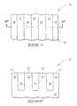
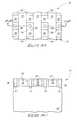
- FIGS. 1 and 2illustrate a semiconductor substrate 12 having shallow trench isolation (STI) regions 14 .
- FIG. 1is a top view of a portion of a memory device 10 at an initial processing stage, wherein the memory device 10 includes the substrate 12 patterned with STI regions 14 and pillars 16 .
- the STI regions 14 and pillars 16alternate in the substrate 12 .
- FIG. 2is a cross-sectional view taken a long line 2 - 2 of FIG. 1 .
- the STI regions 14form pillars 16 in the substrate 12 .
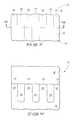
- FIGS. 3 and 4are top and cross-sectional views, respectively, of the memory device 10 at processing stage subsequent to the embodiment illustrated in FIGS. 1 and 2 .
- a nitride layer 18has been deposited on the upper services of the pillars 16 and STI regions 14 .
- the dashed lines in FIG. 3indicate surfaces that are not visible from the top view.
- the pillars 16 and STI regions 14are not visible from the top view illustrated in FIG. 3 , due to the deposition of nitride layer 18 on top of these surfaces.
- the nitride layer 18has a thickness in the range of about 2000 to 3000 Angstroms. In other embodiments, however, the thickness of the nitride layer 18 may be adjusted according to various design parameters.
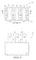
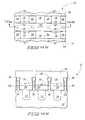
- FIGS. 5-8are views of the memory device 10 at a processing stage subsequent to that of FIGS. 3 and 4 . More particularly, FIGS. 5 and 6 are top and cross-sectional views, respectively, and FIGS. 7 and 8 are top and cross-sectional views, respectively, rotated 90° from the embodiments illustrated in FIGS. 5 and 6 .
- the nitride layer 18has been patterned and etched to form trenches 20 in the nitride layer 18 .
- the trenches 20extend to an upper surface 22 of the substrate 12 .
- the trenches 20also expose isolation region portions 24 of the STI regions 14 . As illustrated in FIGS.
- the nitride layer 18is now patterned so that nitride runners (designated with numeral 18 ) extend vertically from the substrate 12 and are generally separated by the trenches 20 and are parallel to one another.
- nitride runnersdesignated with numeral 18
- the upper surface portions 22 of the substrate 12are generally surrounded by the isolation region portions 24 and the nitride runners 18 .
- the upper surface portions 22are generally shaped as squares.
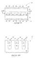
- FIGS. 9-12are views of the memory device 10 at a processing step subsequent to that of FIGS. 5-8 . More particularly, FIGS. 9 and 10 are top and cross-sectional views, respectively, of the memory device 10 and FIGS. 11 and 12 are top and cross-sectional views, respectively, of the memory device 10 rotated 90° from the embodiments illustrated in FIGS. 9 and 10 .
- isolation region portions 24FIG. 6
- the isolation region portions 24are etched using a reactive ion etch (RIE) process to selectively etch material 14 relative to the nitride runners 18 .
- RIEreactive ion etch
- the etch processexposes sidewalls 27 of the substrate 12 which were originally covered by an insulative material deposited in the STI regions 14 .
- the recessed surfaces 26are in the range of about 500 to 1500 Angstroms below the upper surface portions 22 of the substrate 12 . In another embodiment, the recessed surfaces 26 are in the range of about 800 to 1200 Angstroms below the upper surface portions 22 of the substrate 12 . In other embodiments, the recessed surfaces 26 may extend other distances below the upper surface portions 22 .
- etching processfor example, residual oxide on the sidewalls 27 and upper surface portions 22 is removed.
- a wet hydrofluoric (HF) etchis used to remove these residual oxides.
- HFwet hydrofluoric
- other clean etchesmay be used in order to achieve similar results.
- FIGS. 13-16are views of the memory device 10 at a processing step subsequent to that of FIGS. 9-12 . More particularly, FIGS. 13 and 14 are top and cross-sectional views, respectively, of the memory device 10 and FIGS. 15 and 16 are top and cross-sectional views, respectively, of the memory device 10 rotated 90° from the embodiments illustrated in FIGS. 13 and 14 . As illustrated in FIGS. 14 and 16 , for example, a nitride liner 28 has been deposited on the upper surface 22 of the substrate 12 , the recessed surfaces 26 , and the sidewalls 27 . In one embodiment, the nitride liner 28 has a thickness in the range of about 30 to 100 Angstroms.
- a sacrificial layer 30such as a spin-on-glass (SOG), for example, is deposited in the trenches 20 ( FIG. 12 ) between the nitride runners 18 .
- the sacrificial layermay comprise other materials, such as borophosphorous silica glass (BPSG) and/or TEOS.
- the sacrificial layer 30is etched so that the sacrificial layer 30 is planar with the nitride runners 18 .
- the sacrificial layer 30is removed using a chemical mechanical polishing (CMP) process; however other etching processes may be used in order to adjust a height of the sacrificial layer 30 .
- CMPchemical mechanical polishing
- FIGS. 17-20are views of the memory device 10 at a processing step subsequent to that of FIGS. 13-16 . More particularly, FIGS. 17 and 18 are top and cross-sectional views, respectively, of the memory device 10 and FIGS. 19 and 20 are top and cross-sectional views, respectively, of the memory device 10 rotated 90° from the embodiments illustrated in FIGS. 17 and 18 . As illustrated in FIG. 18 , for example, a portion of the sacrificial layer 30 is selectively etched to form opening 31 and to expose the nitride liner 28 over upper surface portions 22 of substrate 12 . The sacrificial layer 30 is selectively etched so that columns 30 remain extending upward above the STI regions 14 . As shown in FIG.
- the exposed portions of the nitride liner 28 on the upper surface portions 22are removed to expose the upper surface portions 22 of the silicon substrate 12 between the columns 30 .
- a selective nitride etchis used to etch the nitride liner 28 from the upper surface portions 22 of the substrate 12 .
- openings 31extend to expose the upper surface portions 22 .
- the exposed upper surface portions 22function as active areas for the memory device 10 .
- FIGS. 21-24are views of the memory device 10 at a processing step subsequent to that of FIGS. 17-20 . More particularly, FIGS. 21 and 22 are top and cross-sectional views, respectively, of the memory device 10 and FIGS. 23 and 24 are top and cross-sectional views, respectively, of the memory device 10 rotated 90° from the embodiments illustrated in FIGS. 21 and 22 . As illustrated in FIGS. 21-24 , insulative spacers 34 have been formed on either side of the sacrificial layer 30 (e.g., FIG. 22 ) and the nitride runners 18 (e.g., FIG. 24 ). In one embodiment, the insulative spacers 34 comprise Tetraethyl Orthosilicate (TEOS).
- TEOSTetraethyl Orthosilicate
- a layer of insulative materialis deposited over the silicon substrate 12 in order to fill the openings 31 ( FIG. 18 ).
- the insulative materialis then anisotropically etched to form the sacrificial insulative spacers 34 .
- a reactive ion etchis used to remove portions of the insulative material, leaving only about 200 to 500 Angstroms of material surrounding the nitride runners 18 and the sacrificial layer 30 .
- the etching of the insulative materialleaves a generally cylindrical openings 32 that expose a smaller surface area of the upper surface portion 22 .
- the insulative spacers 34improve the critical dimensions possible for subsequently formed structures that are formed over or upon upper surface portions 22 of the silicon substrate 12 .
- FIGS. 25-28are views of the memory device 10 at a processing step subsequent to that of FIGS. 21-24 . More particularly, FIGS. 25 and 26 are top and cross-sectional views, respectively, of the memory device 10 and FIGS. 27 and 28 are top and cross-sectional views, respectively, of the memory device 10 rotated 90° from the embodiments illustrated in FIGS. 25 and 26 . As illustrated in FIG. 26 , for example, an additional nitride material 33 is deposited inside the spacers 34 forming nitride plugs 38 that fill the openings 32 ( FIG. 22 ).
- Nitride 33may be formed by depositing a nitride material in the cylindrical openings 32 and then selectively etching (not shown) the nitride material to form nitride plugs 38 inside the sacrificial insulative spacers 34 .
- the nitride plugs 38will have a thickness in the range of about 500 to 1200 Angstroms between the spacers 34 after such selective etching (not shown in FIGS. 25-28 ).
- FIGS. 29-32are views of the memory device 10 at a processing step subsequent to that of FIGS. 25-28 . More particularly, FIGS. 29 and 30 are top and cross-sectional views, respectively, of the memory device 10 and FIGS. 31 and 32 are top and cross-sectional views, respectively, of the memory device 10 rotated 90° from the embodiments illustrated in FIGS. 29 and 30 .
- nitride plugs 38extend upward from the exposed upper surface portions 22 of the silicon substrate 12 in the cylindrical openings.
- upper surfaces of the nitride material 33 of plugs 38 ( FIG. 28 ), nitride runners 18 , and insulative spacers 34are removed using a blanket nitride etch or CMP in order to form the separated nitride plugs 38 from formally interconnected material 33 ( FIGS. 25-28 ).
- the nitride plugs 38are elevationally level with, or below, upper surfaces 47 of the nitride runners 18 .
- FIGS. 33-36are views of the memory device 10 at a processing step subsequent to that of FIGS. 29-32 . More particularly, FIGS. 33 and 34 are top and cross-sectional views, respectively, of the memory device 10 and FIGS. 35 and 36 are top and cross-sectional views, respectively, of the memory device 10 rotated 90° from the embodiments illustrated in FIGS. 33 and 34 . As illustrated in FIGS. 34 and 36 , for example, the sacrificial layers 30 and the insulative spacers 34 (shown in FIG. 30 , for example) have been removed.
- the sacrificial layer 30 and insulative spacers 34are entirely removed using an etching process, such as a diluted hydrofluoric acid etch and/or a buffered oxide etch. In other embodiments, other materials may be used to selectively etch the sacrificial layer 30 and the insulative spacers 34 .
- the selective etchstops etching at nitride and silicon materials, such as the nitride liner 28 , nitride runners 18 , and upper surface portions 22 of silicon substrate 12 . As shown in FIG. 34 , the selective etching forms openings 42 that are defined by nitride liner 28 and nitride runners 18 .
- FIGS. 37-40are views of the memory device 10 at a processing step subsequent to that of FIGS. 33-36 . More particularly, FIGS. 37 and 38 are top and cross-sectional views, respectively, of the memory device 10 and FIGS. 39 and 40 are top and cross-sectional views, respectively, of the memory device 10 rotated 90° from the embodiments illustrated in FIGS. 37 and 38 .
- FIGS. 37-40At the processing stage illustrated in FIGS. 37-40 , at least a portion of the nitride liner 28 , the upper surface portions 22 of substrate 12 , and the STI region 14 are removed using one or more etching processes.
- portions of the nitride plugs 38are also etched when the nitride liner 28 , and substrate 12 , and STI region 14 are etched as described above. Accordingly, in this embodiment, the height of the nitride plugs 38 is decreased due to this etching. After this etching is complete, an insulative film 52 is deposited on the exposed surfaces of the silicon substrate 12 . After completion of these processing steps, which are discussed in further detail below, a channel 21 is created in the silicon substrate 12 , wherein a length of the channel is determined by the depth of the etching.
- a dry/wet nitride punch etchusing, for example, H 3 PO 4 solution, has been used to remove the nitride liner 28 ( FIG. 34 ) from over the STI region 14 , the sidewall of silicon substrate 12 and the upper surface portions 22 of silicon substrate 12 .
- a selective dry etchis used to remove portions of the upper surface portions 22 adjacent the nitride plugs 38 .
- the selective dry etchmay also remove portions of the STI region 14 , while leaving portions of the silicon substrate 12 directly below the nitride plugs 38 .
- the portions of the silicon substrate 12 that remain below the nitride plugs 38are hereinafter referred to as silicon support structures 46 .
- the support structures 46are generally annular or cylindrical shaped, similar to the nitride plugs 38 which extend above the silicon support structures 46 . As illustrated in FIG. 38 , for example, the selective etching enlarges openings 42 ( FIG. 34 ) to form enlarged openings 44 .
- the enlarged openings 44are defined by the silicon support structures 46 , an upper surface 48 of the silicon substrate 12 , and an upper surface 50 of the STI regions 14 .
- the etching processwill remove slightly more of the silicon substrate 12 than the STI region 14 .
- the upper surface 48 of the silicon substrate 12is slightly below the upper surface 50 of the STI regions 14 .
- an insulative film 52is grown over the exposed portions of the silicon substrate 12 and the silicon support structures 46 .
- the insulative film 52comprises an oxide, such as silicon dioxide. Referring to FIG. 38 , for example, the insulative film 52 can be seen covering the side walls of the nitride plugs 38 and the silicon support structures 46 , as well as the upper surface 48 of the silicon substrate 12 .
- the insulative filmserves as a gate oxide dielectric for transistors.
- An exemplary method of forming the dielectricmay include CVD deposition of a low K material on the exposed silicon surfaces of the upper surface 48 of the silicon substrate 12 , the silicon support structures 46 , and the side walls of the nitride plugs 38 .
- the silicon support structures 46serve as a portion of a channel for transistors of the memory device 10 . Accordingly, the length of the silicon support structures 46 defines a vertical length of the transistor channel 21 . In the embodiments illustrated in FIGS. 37-40 , because the transistor channel 21 extends perpendicularly to the orientation of substrate 12 , the transistor channel 21 defines a channel of a vertical transistor.
- FIGS. 41-44are views of the memory device 10 at a processing step subsequent to that of FIGS. 37-40 . More particularly, FIGS. 41 and 42 are top and cross-sectional views, respectively, of the memory device 10 and FIGS. 43 and 44 are top and cross-sectional views, respectively, of the memory device 10 rotated 90° from the embodiments illustrated in FIGS. 41 and 42 .
- diffusion regions 41have been formed below the nitride plugs 38 and transistor gates 54 have been formed over the insulative film 52 .
- the transistor gates 54comprise word lines of the memory device 10 , such as a DRAM.
- an implant methodmay be used to transfer a conductivity dopant through the nitride plugs 38 to the silicon substrate 12 directly beneath the nitride plugs 38 .
- an angle implant methodmay be used to form the diffusion regions 41 .
- Arsenic or Phosphorousmay be implanted in the substrate 12 , below the nitride plugs 38 , angled from within the openings 44 ( FIG. 38 ).
- Any suitable doping methodmay be used to create the diffusion regions 41 .
- the diffusion regions 41are configured to serve as source/drain regions of a transistor device. More generally, the diffusion regions 41 may be used as electrical contacts between charge storage devices, such as capacitors, and other components of a transistor and/or a memory device.
- a conductive material 54such as polysilicon, is deposited on the insulative film 52 and the STI region 14 .
- portions of the deposited conductive materialmay be removed by a polishing process, such as CMP, to an elevation below the silicon nitride plugs 38 .
- CMPpolishing process
- FIG. 42illustrates the upper surfaces 55 of the transistor gate 54 about 1000 Angstroms below the upper surfaces 39 of the silicon nitride plugs 38 .
- the transistor gates 54are recessed from the silicon substrate so that the gate regions are spaced further from the source/drain regions of the transistor devices in the memory 10 .
- the transistor gates 54are recessed below an upper surface of the substrate 12 .
- the transistor gates 54are recessed about 500 Angstroms, or in the range of about 250 to 1,000 Angstroms, below an upper surface of the substrate 12 . Accordingly, cross capacitance between the gate regions and the source/drain regions may be reduced, thus improving the accuracy of the memory device.
- FIGS. 45-48are views of the memory device 10 at a processing step subsequent to that of FIGS. 40-44 . More particularly, FIGS. 45 and 46 are top and cross-sectional views, respectively, of the memory device 10 and FIGS. 47 and 48 are top and cross-sectional views, respectively, of the memory device 10 rotated 90° from the embodiments illustrated in FIGS. 45 and 46 .
- an insulative material 56has been deposited atop the transistor gates 54 ( FIGS. 45 and 46 , for example).
- a conductivity dopantis implanted into the exposed surfaces of the silicon substrate 12 in order to form diffusion regions 59 , which may be transistor sources or drains ( FIGS. 47 and 48 , for example).
- the insulative material 56comprises spin-on-glass (SOG) and TEOS layers. Outermost portions of the insulative layer 56 may be removed by CMP or other planar etching methods to expose nitride runners 18 . Next, the nitride runners 18 are patterned and selectively etched to form opening 62 that extend through portions of the nitride runners 18 down to upper surface portions 58 of substrate 12 .
- a conductivity implantis performed to provide a conductivity dopant into upper surface portions 58 of substrate 12 in order to form active areas 59 .
- the active areas 59comprise source/drain regions of devices such as, for example, transistors.
- FIGS. 49 and 50are views of the memory device 10 at a processing step subsequent to that of FIGS. 45-48 . More particularly, FIGS. 49 and 50 are cross-sectional views, respectively, of the memory device 10 , where FIG. 49 is at the same orientation as FIG. 46 and FIG. 50 is at the same orientation as FIG. 48 .
- FIGS. 49 and 50illustrate transistors electrically coupled to charge storage devices. For example, exemplary transistor 69 is electrically coupled to exemplary capacitor 80 ( FIG. 50 ). The transistor 69 and capacitor 80 combine to form an exemplary memory cell 103 .
- a FET transistortypically comprises a gate, a gate dielectric, a source and drain, and a channel.
- the transistor 69comprises gate 54 , gate dielectric 52 , source/drain regions 41 and 59 , and channel 21 .
- FIG. 50illustrates arrows in the channel 21 which indicate current flow between the source/drain region 59 and the source/drain region 41 .
- activation of the transistor 69establishes a conductivity channel 21 from source/drain region 59 to source/drain region 41 .
- the source/drain region 59comprises a transistor source and the source/drain region 41 comprises a transistor drain.
- the source/drain region 59comprises a transistor drain and the source/drain region 41 comprises a transistor source.
- FIGS. 45-48Several process steps may be performed in order to transform the partially complete memory device 10 illustrated in FIGS. 45-48 to the memory device 100 illustrated in FIGS. 49 and 50 .
- Conductive materialsuch as polysilicon, for example, may then be deposited, forming an electrical contact 102 that couples with the capacitor 80 , for example.
- the transistor 69includes intermediate structures that insulate portions of the transistor 69 from the capacitor 80 .
- the transistor 69comprises a nitride cap 106 and insulative spacers 110 that are formed over the digit line 104 .
- a silicon dioxide layer 108may also be deposited on the nitride caps 106 .
- the capacitor 80comprises a capacitor dielectric 73 over a storage node 72 and a top cell plate 74 over the capacitor dielectric 73 .
- a dielectric plug 63is deposited above the transistor gates 54 and the active areas 59 .
- the dielectric plug 63comprises an oxide material, such as silicon dioxide, for example.
- the dielectric plug 63may then be patterned and etched to form contact holes that expose middle portions of the active areas 59 .
- Metal stackscomprising polysilicon and/or silicide layers, for example, may then be deposited in the contact holes in order to form digit lines 104 .
- the dielectric plug 63moves the digit line 104 conductor away from the silicon support structures 46 .
- the digit lines 104directly contact the active areas 59 so that a conductive plug is not necessary to electrically couple the digit lines 104 with the active areas 59 .
- Such conductive plugsare commonly formed in prior art transistors using epitaxial processes. By removing the need for an additional epitaxial process, the manufacturing defect rate may be decreased.
Landscapes
- Engineering & Computer Science (AREA)
- Manufacturing & Machinery (AREA)
- Semiconductor Memories (AREA)
Abstract
Description
Claims (12)
Priority Applications (2)
| Application Number | Priority Date | Filing Date | Title |
|---|---|---|---|
| US13/469,513US8481385B2 (en) | 2005-08-31 | 2012-05-11 | Methods of fabricating a memory device |
| US13/781,862US8546215B2 (en) | 2005-08-31 | 2013-03-01 | Methods of fabricating a memory device |
Applications Claiming Priority (3)
| Application Number | Priority Date | Filing Date | Title |
|---|---|---|---|
| US11/218,184US7696567B2 (en) | 2005-08-31 | 2005-08-31 | Semiconductor memory device |
| US12/703,502US8222105B2 (en) | 2005-08-31 | 2010-02-10 | Methods of fabricating a memory device |
| US13/469,513US8481385B2 (en) | 2005-08-31 | 2012-05-11 | Methods of fabricating a memory device |
Related Parent Applications (1)
| Application Number | Title | Priority Date | Filing Date |
|---|---|---|---|
| US12/703,502ContinuationUS8222105B2 (en) | 2005-08-31 | 2010-02-10 | Methods of fabricating a memory device |
Related Child Applications (1)
| Application Number | Title | Priority Date | Filing Date |
|---|---|---|---|
| US13/781,862ContinuationUS8546215B2 (en) | 2005-08-31 | 2013-03-01 | Methods of fabricating a memory device |
Publications (2)
| Publication Number | Publication Date |
|---|---|
| US20120231592A1 US20120231592A1 (en) | 2012-09-13 |
| US8481385B2true US8481385B2 (en) | 2013-07-09 |
Family
ID=37829252
Family Applications (4)
| Application Number | Title | Priority Date | Filing Date |
|---|---|---|---|
| US11/218,184Active2027-01-26US7696567B2 (en) | 2005-08-31 | 2005-08-31 | Semiconductor memory device |
| US12/703,502Expired - LifetimeUS8222105B2 (en) | 2005-08-31 | 2010-02-10 | Methods of fabricating a memory device |
| US13/469,513Expired - LifetimeUS8481385B2 (en) | 2005-08-31 | 2012-05-11 | Methods of fabricating a memory device |
| US13/781,862Expired - LifetimeUS8546215B2 (en) | 2005-08-31 | 2013-03-01 | Methods of fabricating a memory device |
Family Applications Before (2)
| Application Number | Title | Priority Date | Filing Date |
|---|---|---|---|
| US11/218,184Active2027-01-26US7696567B2 (en) | 2005-08-31 | 2005-08-31 | Semiconductor memory device |
| US12/703,502Expired - LifetimeUS8222105B2 (en) | 2005-08-31 | 2010-02-10 | Methods of fabricating a memory device |
Family Applications After (1)
| Application Number | Title | Priority Date | Filing Date |
|---|---|---|---|
| US13/781,862Expired - LifetimeUS8546215B2 (en) | 2005-08-31 | 2013-03-01 | Methods of fabricating a memory device |
Country Status (1)
| Country | Link |
|---|---|
| US (4) | US7696567B2 (en) |
Cited By (1)
| Publication number | Priority date | Publication date | Assignee | Title |
|---|---|---|---|---|
| US10818800B2 (en) | 2017-12-22 | 2020-10-27 | Nanya Technology Corporation | Semiconductor structure and method for preparing the same |
Families Citing this family (26)
| Publication number | Priority date | Publication date | Assignee | Title |
|---|---|---|---|---|
| US7547945B2 (en)* | 2004-09-01 | 2009-06-16 | Micron Technology, Inc. | Transistor devices, transistor structures and semiconductor constructions |
| US7384849B2 (en) | 2005-03-25 | 2008-06-10 | Micron Technology, Inc. | Methods of forming recessed access devices associated with semiconductor constructions |
| US7282401B2 (en) | 2005-07-08 | 2007-10-16 | Micron Technology, Inc. | Method and apparatus for a self-aligned recessed access device (RAD) transistor gate |
| US7867851B2 (en) | 2005-08-30 | 2011-01-11 | Micron Technology, Inc. | Methods of forming field effect transistors on substrates |
| US7700441B2 (en)* | 2006-02-02 | 2010-04-20 | Micron Technology, Inc. | Methods of forming field effect transistors, methods of forming field effect transistor gates, methods of forming integrated circuitry comprising a transistor gate array and circuitry peripheral to the gate array, and methods of forming integrated circuitry comprising a transistor gate array including first gates and second grounded isolation gates |
| US7602001B2 (en) | 2006-07-17 | 2009-10-13 | Micron Technology, Inc. | Capacitorless one transistor DRAM cell, integrated circuitry comprising an array of capacitorless one transistor DRAM cells, and method of forming lines of capacitorless one transistor DRAM cells |
| US7772632B2 (en)* | 2006-08-21 | 2010-08-10 | Micron Technology, Inc. | Memory arrays and methods of fabricating memory arrays |
| US7589995B2 (en)* | 2006-09-07 | 2009-09-15 | Micron Technology, Inc. | One-transistor memory cell with bias gate |
| US7858471B2 (en) | 2006-09-13 | 2010-12-28 | Micron Technology, Inc. | Methods of fabricating an access transistor for an integrated circuit device, methods of fabricating periphery transistors and access transistors, and methods of fabricating an access device comprising access transistors in an access circuitry region and peripheral transistors in a peripheral circuitry region spaced from the access circuitry region |
| US7923373B2 (en) | 2007-06-04 | 2011-04-12 | Micron Technology, Inc. | Pitch multiplication using self-assembling materials |
| KR101432619B1 (en)* | 2008-07-07 | 2014-08-21 | 삼성전자주식회사 | Semiconductor device and manufacturing method thereof |
| US8692310B2 (en) | 2009-02-09 | 2014-04-08 | Spansion Llc | Gate fringing effect based channel formation for semiconductor device |
| JP2010219326A (en)* | 2009-03-17 | 2010-09-30 | Elpida Memory Inc | Semiconductor memory device and method of manufacturing the same |
| KR101140051B1 (en)* | 2010-07-01 | 2012-05-02 | 에스케이하이닉스 주식회사 | Semiconductor device and method for forming the same |
| US8750040B2 (en) | 2011-01-21 | 2014-06-10 | Micron Technology, Inc. | Memory devices having source lines directly coupled to body regions and methods |
| US9401363B2 (en)* | 2011-08-23 | 2016-07-26 | Micron Technology, Inc. | Vertical transistor devices, memory arrays, and methods of forming vertical transistor devices |
| US8907396B2 (en) | 2012-01-04 | 2014-12-09 | Micron Technology, Inc | Source/drain zones with a delectric plug over an isolation region between active regions and methods |
| US9064745B2 (en) | 2012-08-29 | 2015-06-23 | International Business Machines Corporation | Sublithographic width finFET employing solid phase epitaxy |
| KR102001417B1 (en) | 2012-10-23 | 2019-07-19 | 삼성전자주식회사 | Semiconductor device |
| US9570447B2 (en)* | 2013-01-23 | 2017-02-14 | Longitude Semiconductor S.A.R.L. | Semiconductor device and production method therefor |
| KR102707534B1 (en) | 2016-12-02 | 2024-09-20 | 삼성전자주식회사 | Semiconductor memory device |
| US10446606B2 (en) | 2017-07-19 | 2019-10-15 | International Business Machines Corporation | Back-side memory element with local memory select transistor |
| US11049864B2 (en)* | 2019-05-17 | 2021-06-29 | Micron Technology, Inc. | Apparatuses including capacitor structures, and related memory devices, electronic systems, and methods |
| US11177266B2 (en) | 2019-08-26 | 2021-11-16 | Micron Technology, Inc. | Array of capacitors, an array of memory cells, a method of forming an array of capacitors, and a method of forming an array of memory cells |
| US11557593B2 (en) | 2020-11-30 | 2023-01-17 | Micron Technology, Inc. | Array of memory cells, methods used in forming an array of memory cells, methods used in forming an array of vertical transistors, and methods used in forming an array of capacitors |
| US11355531B1 (en) | 2020-11-30 | 2022-06-07 | Micron Technology, Inc. | Array of capacitors, an array of memory cells, method used in forming an array of memory cells, methods used in forming an array of capacitors, and methods used in forming a plurality of horizontally-spaced conductive lines |
Citations (368)
| Publication number | Priority date | Publication date | Assignee | Title |
|---|---|---|---|---|
| US3731287A (en) | 1971-07-02 | 1973-05-01 | Gen Instrument Corp | Single device memory system having shift register output characteristics |
| US3732287A (en) | 1969-09-09 | 1973-05-08 | Basf Ag | Bismonocarboxylic esters of 3-formylbutanediol-1,2 |
| US3941629A (en) | 1974-04-11 | 1976-03-02 | General Motors Corporation | Diaphragm formation on silicon substrate |
| US4139442A (en) | 1977-09-13 | 1979-02-13 | International Business Machines Corporation | Reactive ion etching method for producing deep dielectric isolation in silicon |
| US4234362A (en) | 1978-11-03 | 1980-11-18 | International Business Machines Corporation | Method for forming an insulator between layers of conductive material |
| US4333964A (en) | 1980-09-15 | 1982-06-08 | General Electric Company | Method of making integrated circuits |
| US4419809A (en) | 1981-12-30 | 1983-12-13 | International Business Machines Corporation | Fabrication process of sub-micrometer channel length MOSFETs |
| US4432132A (en) | 1981-12-07 | 1984-02-21 | Bell Telephone Laboratories, Incorporated | Formation of sidewall oxide layers by reactive oxygen ion etching to define submicron features |
| US4470062A (en) | 1979-08-31 | 1984-09-04 | Hitachi, Ltd. | Semiconductor device having isolation regions |
| US4472459A (en) | 1983-10-24 | 1984-09-18 | Rca Corporation | Local oxidation of silicon substrate using LPCVD silicon nitride |
| US4502914A (en) | 1982-11-13 | 1985-03-05 | International Business Machines Corporation | Method of making structures with dimensions in the sub-micrometer range |
| US4508757A (en) | 1982-12-20 | 1985-04-02 | International Business Machines Corporation | Method of manufacturing a minimum bird's beak recessed oxide isolation structure |
| US4551910A (en) | 1984-11-27 | 1985-11-12 | Intel Corporation | MOS Isolation processing |
| US4570325A (en) | 1983-12-16 | 1986-02-18 | Kabushiki Kaisha Toshiba | Manufacturing a field oxide region for a semiconductor device |
| US4615762A (en) | 1985-04-30 | 1986-10-07 | Rca Corporation | Method for thinning silicon |
| US4630356A (en) | 1985-09-19 | 1986-12-23 | International Business Machines Corporation | Method of forming recessed oxide isolation with reduced steepness of the birds' neck |
| US4648937A (en) | 1985-10-30 | 1987-03-10 | International Business Machines Corporation | Method of preventing asymmetric etching of lines in sub-micrometer range sidewall images transfer |
| EP0227303A2 (en) | 1985-11-25 | 1987-07-01 | Plessey Overseas Limited | Method of manufacturing semiconductor devices having side-wall isolation |
| US4716131A (en) | 1983-11-28 | 1987-12-29 | Nec Corporation | Method of manufacturing semiconductor device having polycrystalline silicon layer with metal silicide film |
| US4746630A (en) | 1986-09-17 | 1988-05-24 | Hewlett-Packard Company | Method for producing recessed field oxide with improved sidewall characteristics |
| US4776922A (en) | 1987-10-30 | 1988-10-11 | International Business Machines Corporation | Formation of variable-width sidewall structures |
| US4789560A (en) | 1986-01-08 | 1988-12-06 | Advanced Micro Devices, Inc. | Diffusion stop method for forming silicon oxide during the fabrication of IC devices |
| US4838991A (en) | 1987-10-30 | 1989-06-13 | International Business Machines Corporation | Process for defining organic sidewall structures |
| US4903344A (en) | 1987-07-07 | 1990-02-20 | Oki Electric Industry Co., Ltd. | Semiconductor memory device with staggered sense amplifiers |
| US4959325A (en) | 1989-02-24 | 1990-09-25 | Micron Technology, Inc. | Reduction of electric field effect in the bird's beak region of a DRAM cell following expansion of active region through local encroachment reduction |
| US4965221A (en) | 1989-03-15 | 1990-10-23 | Micron Technology, Inc. | Spacer isolation method for minimizing parasitic sidewall capacitance and creating fully recessed field oxide regions |
| US4983544A (en) | 1986-10-20 | 1991-01-08 | International Business Machines Corporation | Silicide bridge contact process |
| US5013680A (en) | 1990-07-18 | 1991-05-07 | Micron Technology, Inc. | Process for fabricating a DRAM array having feature widths that transcend the resolution limit of available photolithography |
| US5041898A (en) | 1987-09-08 | 1991-08-20 | Mitsubishi Denki Kabushiki Kaisha | Interconnection layer formed on embedded dielectric and method for manufacturing the same |
| US5047117A (en) | 1990-09-26 | 1991-09-10 | Micron Technology, Inc. | Method of forming a narrow self-aligned, annular opening in a masking layer |
| US5053105A (en) | 1990-07-19 | 1991-10-01 | Micron Technology, Inc. | Process for creating an etch mask suitable for deep plasma etches employing self-aligned silicidation of a metal layer masked with a silicon dioxide template |
| US5057449A (en) | 1990-03-26 | 1991-10-15 | Micron Technology, Inc. | Process for creating two thicknesses of gate oxide within a dynamic random access memory |
| US5087586A (en) | 1991-07-03 | 1992-02-11 | Micron Technology, Inc. | Process for creating fully-recessed field isolation regions by oxidizing a selectively-grown epitaxial silicon layer |
| US5117027A (en) | 1990-10-31 | 1992-05-26 | Huls Aktiengesellschaft | Process for the preparation of organosilanes containing methacryloyloxy or acryloyloxy groups |
| US5122848A (en) | 1991-04-08 | 1992-06-16 | Micron Technology, Inc. | Insulated-gate vertical field-effect transistor with high current drive and minimum overlap capacitance |
| US5128274A (en) | 1989-08-01 | 1992-07-07 | Matsushita Electric Industrial Co., Ltd. | Method for producing a semiconductor device having a LOCOS insulating film with at least two different thickness |
| US5149669A (en) | 1987-03-06 | 1992-09-22 | Seiko Instruments Inc. | Method of forming an isolation region in a semiconductor device |
| EP0491408A3 (en) | 1990-11-20 | 1992-10-28 | Consorzio Per La Ricerca Sulla Microelettronica Nel Mezzogiorno | Process for making planarized sub-micrometric trenches in integrated circuits |
| US5177027A (en) | 1990-08-17 | 1993-01-05 | Micron Technology, Inc. | Process for fabricating, on the edge of a silicon mesa, a MOSFET which has a spacer-shaped gate and a right-angled channel path |
| US5210046A (en) | 1989-12-22 | 1993-05-11 | Scs-Thomas Microelectronics S.R.L. | Method of fabricating eprom device with metallic source connections |
| US5250450A (en) | 1991-04-08 | 1993-10-05 | Micron Technology, Inc. | Insulated-gate vertical field-effect transistor with high current drive and minimum overlap capacitance |
| US5252504A (en) | 1988-05-02 | 1993-10-12 | Micron Technology, Inc. | Reverse polysilicon CMOS fabrication |
| US5260229A (en) | 1991-08-30 | 1993-11-09 | Sgs-Thomson Microelectronics, Inc. | Method of forming isolated regions of oxide |
| US5295092A (en) | 1992-01-21 | 1994-03-15 | Sharp Kabushiki Kaisha | Semiconductor read only memory |
| US5305252A (en) | 1990-07-06 | 1994-04-19 | Nec Corporation | Semiconductor memory device having memory cell matrix obliquely arranged with respect to bit lines |
| DE4236609A1 (en) | 1992-10-29 | 1994-05-05 | Siemens Ag | Method for forming a structure in the surface of a substrate - with an auxiliary structure laterally bounding an initial masking structure, followed by selective removal of masking structure using the auxiliary structure as an etching mask |
| US5316966A (en) | 1990-09-28 | 1994-05-31 | U.S. Philips Corporation | Method of providing mask alignment marks |
| US5319753A (en) | 1992-09-29 | 1994-06-07 | Zilog, Inc. | Queued interrupt mechanism with supplementary command/status/message information |
| US5328810A (en) | 1990-05-07 | 1994-07-12 | Micron Technology, Inc. | Method for reducing, by a factor or 2-N, the minimum masking pitch of a photolithographic process |
| US5330879A (en) | 1992-07-16 | 1994-07-19 | Micron Technology, Inc. | Method for fabrication of close-tolerance lines and sharp emission tips on a semiconductor wafer |
| US5334548A (en) | 1988-06-01 | 1994-08-02 | Texas Instruments Incorporated | High performance composed pillar dRAM cell |
| US5358894A (en) | 1992-02-06 | 1994-10-25 | Micron Technology, Inc. | Oxidation enhancement in narrow masked field regions of a semiconductor wafer |
| US5409563A (en) | 1993-02-26 | 1995-04-25 | Micron Technology, Inc. | Method for etching high aspect ratio features |
| US5414287A (en) | 1994-04-25 | 1995-05-09 | United Microelectronics Corporation | Process for high density split-gate memory cell for flash or EPROM |
| US5416350A (en) | 1993-03-15 | 1995-05-16 | Kabushiki Kaisha Toshiba | Semiconductor device with vertical transistors connected in series between bit lines |
| US5438016A (en) | 1994-03-02 | 1995-08-01 | Micron Semiconductor, Inc. | Method of semiconductor device isolation employing polysilicon layer for field oxide formation |
| US5457067A (en) | 1993-10-14 | 1995-10-10 | Goldstar Electron Co., Ltd. | Process for formation of an isolating layer for a semiconductor device |
| US5458999A (en) | 1993-06-24 | 1995-10-17 | Szabo; Gabor | Interferometric phase shifting method for high resolution microlithography |
| US5466632A (en) | 1994-05-26 | 1995-11-14 | United Microelectronics Corp. | Field oxide with curvilinear boundaries and method of producing the same |
| US5468675A (en) | 1993-05-26 | 1995-11-21 | Rohm Co., Ltd. | Method for manufacturing a device separation region for semiconductor device |
| US5497017A (en) | 1995-01-26 | 1996-03-05 | Micron Technology, Inc. | Dynamic random access memory array having a cross-point layout, tungsten digit lines buried in the substrate, and vertical access transistors |
| US5502320A (en) | 1993-03-15 | 1996-03-26 | Kabushiki Kaisha Toshiba | Dynamic random access memory (DRAM) semiconductor device |
| US5514885A (en) | 1986-10-09 | 1996-05-07 | Myrick; James J. | SOI methods and apparatus |
| US5539229A (en) | 1994-12-28 | 1996-07-23 | International Business Machines Corporation | MOSFET with raised STI isolation self-aligned to the gate stack |
| US5563012A (en) | 1994-06-30 | 1996-10-08 | International Business Machines Corporation | Multi mask method for selective mask feature enhancement |
| US5569620A (en) | 1992-09-03 | 1996-10-29 | Harris Corporation | Bonded wafer processing with metal silicidation |
| US5583065A (en) | 1994-11-23 | 1996-12-10 | Sony Corporation | Method of making a MOS semiconductor device |
| US5596759A (en) | 1989-11-03 | 1997-01-21 | Compaq Computer Corporation | Method for initializing a multiple processor computer system using a common ROM |
| US5604159A (en) | 1994-01-31 | 1997-02-18 | Motorola, Inc. | Method of making a contact structure |
| US5607874A (en) | 1996-02-02 | 1997-03-04 | Taiwan Semiconductor Manufacturing Company, Ltd. | Method for fabricating a DRAM cell with a T shaped storage capacitor |
| US5638318A (en) | 1995-09-11 | 1997-06-10 | Micron Technology, Inc. | Ferroelectric memory using ferroelectric reference cells |
| US5670794A (en) | 1994-10-07 | 1997-09-23 | Micron Technology, Inc. | Thin film transistors |
| US5675164A (en) | 1995-06-07 | 1997-10-07 | International Business Machines Corporation | High performance multi-mesa field effect transistor |
| US5677865A (en) | 1995-09-11 | 1997-10-14 | Micron Technology, Inc. | Ferroelectric memory using reference charge circuit |
| US5680344A (en) | 1995-09-11 | 1997-10-21 | Micron Technology, Inc. | Circuit and method of operating a ferrolectric memory in a DRAM mode |
| US5679591A (en) | 1996-12-16 | 1997-10-21 | Taiwan Semiconductor Manufacturing Company, Ltd | Method of making raised-bitline contactless trenched flash memory cell |
| US5700733A (en) | 1995-06-27 | 1997-12-23 | Micron Technology, Inc. | Semiconductor processing methods of forming field oxide regions on a semiconductor substrate |
| US5705321A (en) | 1993-09-30 | 1998-01-06 | The University Of New Mexico | Method for manufacture of quantum sized periodic structures in Si materials |
| US5747377A (en) | 1996-09-06 | 1998-05-05 | Powerchip Semiconductor Corp. | Process for forming shallow trench isolation |
| US5748519A (en) | 1996-12-13 | 1998-05-05 | Motorola, Inc. | Method of selecting a memory cell in a magnetic random access memory device |
| US5753546A (en) | 1995-06-30 | 1998-05-19 | Hyundai Electronics Industries Co., Ltd. | Method for fabricating metal oxide field effect transistors |
| US5756395A (en) | 1995-08-18 | 1998-05-26 | Lsi Logic Corporation | Process for forming metal interconnect structures for use with integrated circuit devices to form integrated circuit structures |
| US5780349A (en) | 1997-02-20 | 1998-07-14 | National Semiconductor Corporation | Self-aligned MOSFET gate/source/drain salicide formation |
| US5789306A (en) | 1996-04-18 | 1998-08-04 | Micron Technology, Inc. | Dual-masked field isolation |
| US5789269A (en) | 1995-07-11 | 1998-08-04 | Advanced Micro Devices, Inc. | Field implant for semiconductor device |
| US5789320A (en) | 1996-04-23 | 1998-08-04 | International Business Machines Corporation | Plating of noble metal electrodes for DRAM and FRAM |
| US5795830A (en) | 1995-06-06 | 1998-08-18 | International Business Machines Corporation | Reducing pitch with continuously adjustable line and space dimensions |
| US5804458A (en) | 1996-12-16 | 1998-09-08 | Motorola, Inc. | Method of fabricating spaced apart submicron magnetic memory cells |
| US5821600A (en) | 1994-12-20 | 1998-10-13 | Stmicroelectronics, Inc. | Isolation by active transistors with grounded gates |
| US5834359A (en) | 1997-08-29 | 1998-11-10 | Vanguard International Semiconductor Corporation | Method of forming an isolation region in a semiconductor substrate |
| US5841611A (en) | 1994-05-02 | 1998-11-24 | Matsushita Electric Industrial Co., Ltd. | Magnetoresistance effect device and magnetoresistance effect type head, memory device, and amplifying device using the same |
| US5861328A (en) | 1996-10-07 | 1999-01-19 | Motorola, Inc. | Method of fabricating GMR devices |
| US5864496A (en) | 1997-09-29 | 1999-01-26 | Siemens Aktiengesellschaft | High density semiconductor memory having diagonal bit lines and dual word lines |
| US5892708A (en) | 1992-09-24 | 1999-04-06 | Nonvolatile Electronics, Incorporated | Magnetoresistive memory using large fraction of memory cell films for data storage |
| US5895273A (en) | 1997-06-27 | 1999-04-20 | International Business Machines Corporation | Silicon sidewall etching |
| US5895238A (en) | 1996-12-12 | 1999-04-20 | Nec Corporation | Doping technique for MOS devices |
| US5899727A (en) | 1996-05-02 | 1999-05-04 | Advanced Micro Devices, Inc. | Method of making a semiconductor isolation region bounded by a trench and covered with an oxide to improve planarization |
| US5902690A (en) | 1997-02-25 | 1999-05-11 | Motorola, Inc. | Stray magnetic shielding for a non-volatile MRAM |
| US5905285A (en) | 1996-09-12 | 1999-05-18 | Advanced Micro Devices, Inc. | Ultra short trench transistors and process for making same |
| US5907170A (en) | 1997-10-06 | 1999-05-25 | Micron Technology, Inc. | Circuit and method for an open bit line memory cell with a vertical transistor and trench plate trench capacitor |
| US5909618A (en) | 1997-07-08 | 1999-06-01 | Micron Technology, Inc. | Method of making memory cell with vertical transistor and buried word and body lines |
| US5917745A (en) | 1997-09-18 | 1999-06-29 | Fujitsu Limited | Semiconductor memory device |
| US5917749A (en) | 1997-05-23 | 1999-06-29 | Motorola, Inc. | MRAM cell requiring low switching field |
| US5956267A (en) | 1997-12-18 | 1999-09-21 | Honeywell Inc | Self-aligned wordline keeper and method of manufacture therefor |
| US5963469A (en) | 1998-02-24 | 1999-10-05 | Micron Technology, Inc. | Vertical bipolar read access for low voltage memory cell |
| US5963803A (en) | 1998-02-02 | 1999-10-05 | Advanced Micro Devices, Inc. | Method of making N-channel and P-channel IGFETs with different gate thicknesses and spacer widths |
| US5977579A (en) | 1998-12-03 | 1999-11-02 | Micron Technology, Inc. | Trench dram cell with vertical device and buried word lines |
| US5998256A (en) | 1996-11-01 | 1999-12-07 | Micron Technology, Inc. | Semiconductor processing methods of forming devices on a substrate, forming device arrays on a substrate, forming conductive lines on a substrate, and forming capacitor arrays on a substrate, and integrated circuitry |
| US6004862A (en) | 1998-01-20 | 1999-12-21 | Advanced Micro Devices, Inc. | Core array and periphery isolation technique |
| US6005800A (en) | 1998-11-23 | 1999-12-21 | International Business Machines Corporation | Magnetic memory array with paired asymmetric memory cells for improved write margin |
| US6008106A (en) | 1997-07-15 | 1999-12-28 | Mosel Vitelic Inc. | Micro-trench oxidation by using rough oxide mask for field isolation |
| US6010946A (en) | 1996-08-21 | 2000-01-04 | Nec Corporation | Semiconductor device with isolation insulating film tapered and method of manufacturing the same |
| US6042998A (en) | 1993-09-30 | 2000-03-28 | The University Of New Mexico | Method and apparatus for extending spatial frequencies in photolithography images |
| US6049106A (en) | 1999-01-14 | 2000-04-11 | Micron Technology, Inc. | Large grain single crystal vertical thin film polysilicon MOSFETs |
| US6057573A (en) | 1998-05-27 | 2000-05-02 | Vanguard International Semiconductor Corporation | Design for high density memory with relaxed metal pitch |
| US6063688A (en) | 1997-09-29 | 2000-05-16 | Intel Corporation | Fabrication of deep submicron structures and quantum wire transistors using hard-mask transistor width definition |
| US6066869A (en) | 1997-10-06 | 2000-05-23 | Micron Technology, Inc. | Circuit and method for a folded bit line memory cell with vertical transistor and trench capacitor |
| US6066191A (en) | 1997-05-21 | 2000-05-23 | Kabushiki Kaisha Toyota Chuo Kenkyusho | Hard molybdenum alloy, wear resistant alloy and method for manufacturing the same |
| US6071789A (en) | 1998-11-10 | 2000-06-06 | Vanguard International Semiconductor Corporation | Method for simultaneously fabricating a DRAM capacitor and metal interconnections |
| US6072209A (en) | 1997-07-08 | 2000-06-06 | Micro Technology, Inc. | Four F2 folded bit line DRAM cell structure having buried bit and word lines |
| US6077745A (en) | 1997-01-22 | 2000-06-20 | International Business Machines Corporation | Self-aligned diffused source vertical transistors with stack capacitors in a 4F-square memory cell array |
| DE19928781C1 (en) | 1999-06-23 | 2000-07-06 | Siemens Ag | DRAM cell array has deep word line trenches for increasing transistor channel length and has no fixed potential word lines separating adjacent memory cells |
| US6097065A (en) | 1998-03-30 | 2000-08-01 | Micron Technology, Inc. | Circuits and methods for dual-gated transistors |
| US6104633A (en) | 1998-02-10 | 2000-08-15 | International Business Machines Corporation | Intentional asymmetry imposed during fabrication and/or access of magnetic tunnel junction devices |
| US6104068A (en) | 1998-09-01 | 2000-08-15 | Micron Technology, Inc. | Structure and method for improved signal processing |
| US6121148A (en) | 1998-02-17 | 2000-09-19 | National Semiconductor Corporation | Semiconductor device trench isolation structure with polysilicon bias voltage contact |
| US6134139A (en) | 1999-07-28 | 2000-10-17 | Hewlett-Packard | Magnetic memory structure with improved half-select margin |
| US6141204A (en) | 1996-01-03 | 2000-10-31 | Micron Technology, Inc. | Capacitor constructions and semiconductor processing method of forming capacitor constructions |
| US6147405A (en) | 1998-02-19 | 2000-11-14 | Micron Technology, Inc. | Asymmetric, double-sided self-aligned silicide and method of forming the same |
| US6150211A (en) | 1996-12-11 | 2000-11-21 | Micron Technology, Inc. | Methods of forming storage capacitors in integrated circuitry memory cells and integrated circuitry |
| US6150687A (en) | 1997-07-08 | 2000-11-21 | Micron Technology, Inc. | Memory cell having a vertical transistor with buried source/drain and dual gates |
| US6150688A (en) | 1994-05-26 | 2000-11-21 | Mitsubishi Denki Kabushiki Kaisha | Semiconductor device and method of manufacturing the same |
| US6157064A (en) | 1997-12-15 | 2000-12-05 | Taiwan Semiconductor Manufacturing Company Ltd. | Method and a deep sub-micron field effect transistor structure for suppressing short channel effects |
| EP1061592A2 (en) | 1999-06-17 | 2000-12-20 | Matsushita Electric Industrial Co., Ltd. | Magneto-resistance effect element, and its use as memory element |
| US6165833A (en) | 1997-12-19 | 2000-12-26 | Micron Technology, Inc. | Semiconductor processing method of forming a capacitor |
| US6172391B1 (en) | 1997-08-27 | 2001-01-09 | Siemens Aktiengesellschaft | DRAM cell arrangement and method for the manufacture thereof |
| US6174780B1 (en) | 1996-04-08 | 2001-01-16 | Micron Technology, Inc. | Method of preparing integrated circuit devices containing isolated dielectric material |
| US6175146B1 (en) | 1997-03-13 | 2001-01-16 | Micron Technology, Inc. | Semiconductor processing methods of forming integrated circuitry memory devices, methods of forming capacitor containers, methods of making electrical connection to circuit nodes and related integrated circuitry |
| US6191470B1 (en) | 1997-07-08 | 2001-02-20 | Micron Technology, Inc. | Semiconductor-on-insulator memory cell with buried word and body lines |
| US6211044B1 (en) | 1999-04-12 | 2001-04-03 | Advanced Micro Devices | Process for fabricating a semiconductor device component using a selective silicidation reaction |
| US6229169B1 (en) | 1997-12-17 | 2001-05-08 | Infineon Technologies Ag | Memory cell configuration, method for fabricating it and methods for operating it |
| US6236590B1 (en) | 2000-07-21 | 2001-05-22 | Hewlett-Packard Company | Optimal write conductors layout for improved performance in MRAM |
| US6238976B1 (en) | 1997-07-08 | 2001-05-29 | Micron Technology, Inc. | Method for forming high density flash memory |
| US6246083B1 (en) | 1998-02-24 | 2001-06-12 | Micron Technology, Inc. | Vertical gain cell and array for a dynamic random access memory |
| US20010005631A1 (en) | 1999-12-14 | 2001-06-28 | Jin-Won Kim | Method for manufacturing an electrode of a capacitor |
| US6265742B1 (en) | 1998-03-04 | 2001-07-24 | Siemens Aktiengesellschaft | Memory cell structure and fabrication |
| US6271080B1 (en) | 1999-12-16 | 2001-08-07 | International Business Machines Corporation | Structure and method for planar MOSFET DRAM cell free of wordline gate conductor to storage trench overlay sensitivity |
| US6274905B1 (en) | 1999-06-30 | 2001-08-14 | Fairchild Semiconductor Corporation | Trench structure substantially filled with high-conductivity material |
| US6282113B1 (en) | 1999-09-29 | 2001-08-28 | International Business Machines Corporation | Four F-squared gapless dual layer bitline DRAM array architecture |
| US20010019870A1 (en) | 1997-04-25 | 2001-09-06 | Noble Wendell P. | Semiconductor processing methods of forming integrated circuitry, forming conductive lines, forming a conductive grid, forming a conductive network, forming an electrical interconnection to a node location forming an electrical interconnection with a transistor source/drain region, and integrated circuitry |
| US6288454B1 (en) | 1999-05-13 | 2001-09-11 | Lsi Logic Corporation | Semiconductor wafer having a layer-to-layer alignment mark and method for fabricating the same |
| US6291334B1 (en) | 1997-12-19 | 2001-09-18 | Applied Materials, Inc. | Etch stop layer for dual damascene process |
| US6297554B1 (en) | 2000-03-10 | 2001-10-02 | United Microelectronics Corp. | Dual damascene interconnect structure with reduced parasitic capacitance |
| US6306727B1 (en) | 1997-08-18 | 2001-10-23 | Micron Technology, Inc. | Advanced isolation process for large memory arrays |
| US6316309B1 (en) | 1998-06-09 | 2001-11-13 | Steven John Holmes | Method of forming self-isolated and self-aligned 4F-square vertical FET-trench DRAM cells |
| US6320222B1 (en) | 1998-09-01 | 2001-11-20 | Micron Technology, Inc. | Structure and method for reducing threshold voltage variations due to dopant fluctuations |
| US20020000608A1 (en) | 2000-06-02 | 2002-01-03 | Hirofumi Harada | Vertical MOS transistor and a method of manufacturing the same |
| US20020005590A1 (en) | 1996-01-26 | 2002-01-17 | Brent Keeth | Digit line architecture for dynamic memory |
| US6348380B1 (en) | 2000-08-25 | 2002-02-19 | Micron Technology, Inc. | Use of dilute steam ambient for improvement of flash devices |
| US20020024081A1 (en) | 2000-08-27 | 2002-02-28 | Achim Gratz | Vertical non-volatile semiconductor memory cell and method for manufaturing the memory cell |
| US20020028541A1 (en) | 2000-08-14 | 2002-03-07 | Lee Thomas H. | Dense arrays and charge storage devices, and methods for making same |
| US20020030214A1 (en) | 2000-09-11 | 2002-03-14 | Fumio Horiguchi | Semiconductor device and method for manufacturing the same |
| US6362057B1 (en) | 1999-10-26 | 2002-03-26 | Motorola, Inc. | Method for forming a semiconductor device |
| US20020038886A1 (en) | 1999-03-31 | 2002-04-04 | Mo Brian Sze-Ki | Method of forming trench transistor with self-aligned source |
| US6368950B1 (en) | 2000-12-12 | 2002-04-09 | Advanced Micro Devices, Inc. | Silicide gate transistors |
| US20020042198A1 (en) | 2000-09-20 | 2002-04-11 | Bjarni Bjarnason | Method in etching of a substrate |
| US20020045308A1 (en) | 1996-11-01 | 2002-04-18 | Werner Juengling | Semiconductor processing methods of forming a plurality of capacitors on a substrate, bit line contacts and method of forming bit line contacts |
| US6377070B1 (en) | 2001-02-09 | 2002-04-23 | Micron Technology, Inc. | In-service programmable logic arrays with ultra thin vertical body transistors |
| US6383907B1 (en) | 1999-09-08 | 2002-05-07 | Sony Corporation | Process for fabricating a semiconductor device |
| US6391782B1 (en) | 2000-06-20 | 2002-05-21 | Advanced Micro Devices, Inc. | Process for forming multiple active lines and gate-all-around MOSFET |
| US20020061639A1 (en) | 2000-10-02 | 2002-05-23 | Kazuichiroh Itonaga | Semiconductor device and method for manufacturing the same |
| US6396096B1 (en) | 2000-06-21 | 2002-05-28 | International Business Machines Corporation | Design layout for a dense memory cell structure |
| US20020063110A1 (en) | 2000-11-30 | 2002-05-30 | Cantell Marc W. | Etching of hard masks |
| US6404056B1 (en) | 1994-01-20 | 2002-06-11 | Mitsubishi Denki Kabushiki Kaisha | Semiconductor integrated circuit |
| US6424001B1 (en) | 2001-02-09 | 2002-07-23 | Micron Technology, Inc. | Flash memory with ultra thin vertical body transistors |
| US6424561B1 (en) | 2000-07-18 | 2002-07-23 | Micron Technology, Inc. | MRAM architecture using offset bits for increased write selectivity |
| US6423474B1 (en) | 2000-03-21 | 2002-07-23 | Micron Technology, Inc. | Use of DARC and BARC in flash memory processing |
| US20020106772A1 (en) | 1998-10-15 | 2002-08-08 | Washington State University Research Foundation | Geranyl diphosphate synthase large subunit, and methods of use |
| US6440801B1 (en) | 1997-01-22 | 2002-08-27 | International Business Machines Corporation | Structure for folded architecture pillar memory cell |
| US20020123216A1 (en) | 2001-03-05 | 2002-09-05 | Natsuki Yokoyama | Method of manufacturing semiconductor device |
| US20020121673A1 (en) | 2000-08-31 | 2002-09-05 | Keiji Jono | Methods of forming an isolation trench in a semiconductor, methods of forming an isolation trench in a surface of a silicon wafer, methods of forming an isolation trench-isolated transistor, trench-isolated transistor, trench isolation structures formed in a semiconductor, memory cells and DRAMs |
| US6448601B1 (en) | 2001-02-09 | 2002-09-10 | Micron Technology, Inc. | Memory address and decode circuits with ultra thin body transistors |
| US20020125536A1 (en) | 1997-04-04 | 2002-09-12 | Nippon Steel Corporation | Semiconductor device and a method of manufacturing the same |
| US20020127810A1 (en) | 2000-05-29 | 2002-09-12 | Fujitsu Limited | Semiconductor device and method for fabricating the same |
| US20020130348A1 (en) | 2001-03-16 | 2002-09-19 | Tran Luan C. | 6F2 dram array, a dram array formed on a semiconductive substrate, a method of forming memory cells in a 6F2 dram array and a method of isolating a single row of memory cells in a 6F2 dram array |
| US20020130686A1 (en) | 2001-03-14 | 2002-09-19 | Micron Technology, Inc. | CMOS gate array with vertical transistors |
| US6455372B1 (en) | 2000-08-14 | 2002-09-24 | Micron Technology, Inc. | Nucleation for improved flash erase characteristics |
| US20020135029A1 (en) | 2001-03-23 | 2002-09-26 | Er-Xuan Ping | Method for forming raised structures by controlled selective epitaxial growth of facet using spacer |
| US6459119B1 (en) | 1998-06-09 | 2002-10-01 | Macronix International Co., Ltd. | Contact array structure for buried type transistor |
| US6458662B1 (en) | 2001-04-04 | 2002-10-01 | Advanced Micro Devices, Inc. | Method of fabricating a semiconductor device having an asymmetrical dual-gate silicon-germanium (SiGe) channel MOSFET and a device thereby formed |
| US6475874B2 (en) | 2000-12-07 | 2002-11-05 | Advanced Micro Devices, Inc. | Damascene NiSi metal gate high-k transistor |
| US6475894B1 (en) | 2002-01-18 | 2002-11-05 | Nanya Technology Corporation | Process for fabricating a floating gate of a flash memory in a self-aligned manner |
| US6475869B1 (en) | 2001-02-26 | 2002-11-05 | Advanced Micro Devices, Inc. | Method of forming a double gate transistor having an epitaxial silicon/germanium channel region |
| WO2002099864A1 (en) | 2001-05-31 | 2002-12-12 | Infineon Technologies, Ag | Method for removing polysilane from a semiconductor without stripping |
| US6496034B2 (en) | 2001-02-09 | 2002-12-17 | Micron Technology, Inc. | Programmable logic arrays with ultra thin body transistors |
| US6498062B2 (en) | 2001-04-27 | 2002-12-24 | Micron Technology, Inc. | DRAM access transistor |
| US20030001290A1 (en) | 2001-06-29 | 2003-01-02 | Kabushiki Kaisha Toshiba | Semiconductor memory device and method for manufacturing the same |
| US20030006410A1 (en) | 2000-03-01 | 2003-01-09 | Brian Doyle | Quantum wire gate device and method of making same |
| US20030015757A1 (en) | 2001-07-19 | 2003-01-23 | Takashi Ohsawa | Semiconductor memory device |
| US6514884B2 (en) | 1998-02-06 | 2003-02-04 | Semiconductor Process Laboratory Co., Ltd. | Method for reforming base surface, method for manufacturing semiconductor device and equipment for manufacturing the same |
| US6522584B1 (en) | 2001-08-02 | 2003-02-18 | Micron Technology, Inc. | Programming methods for multi-level flash EEPROMs |
| US20030040186A1 (en) | 1999-03-23 | 2003-02-27 | Micron Technology, Inc. | Methods of forming materials over uneven surface topologies, and methods of forming insulative materials over and between conductive lines |
| US20030044722A1 (en) | 2001-08-28 | 2003-03-06 | Yi-Yu Hsu | Process for improving critical dimension uniformity |
| US20030042542A1 (en) | 1996-04-26 | 2003-03-06 | Shigeto Maegawa | Semiconductor device having a thin film transistor and manufacturing method thereof |
| US6531727B2 (en) | 2001-02-09 | 2003-03-11 | Micron Technology, Inc. | Open bit line DRAM with ultra thin body transistors |
| US6534243B1 (en) | 2000-10-23 | 2003-03-18 | Advanced Micro Devices, Inc. | Chemical feature doubling process |
| US6537870B1 (en) | 2000-09-29 | 2003-03-25 | Infineon Technologies Ag | Method of forming an integrated circuit comprising a self aligned trench |
| US6548396B2 (en) | 1998-07-23 | 2003-04-15 | Applied Materials, Inc. | Method of producing an interconnect structure for an integrated circuit |
| US6551878B2 (en) | 1998-09-03 | 2003-04-22 | Micron Technology, Inc. | Mini flash process and circuit |
| US20030077855A1 (en) | 2001-10-24 | 2003-04-24 | Abbott Todd R. | Integrated circuitry and method of forming local interconnects |
| US6559491B2 (en) | 2001-02-09 | 2003-05-06 | Micron Technology, Inc. | Folded bit line DRAM with ultra thin body transistors |
| US6559017B1 (en) | 2002-06-13 | 2003-05-06 | Advanced Micro Devices, Inc. | Method of using amorphous carbon as spacer material in a disposable spacer process |
| US20030085422A1 (en) | 2001-09-05 | 2003-05-08 | International Rectifier Corp. | Trench fet with self aligned source and contact |
| US6566682B2 (en) | 2001-02-09 | 2003-05-20 | Micron Technology, Inc. | Programmable memory address and decode circuits with ultra thin vertical body transistors |
| US6566280B1 (en) | 2002-08-26 | 2003-05-20 | Intel Corporation | Forming polymer features on a substrate |
| US6573030B1 (en) | 2000-02-17 | 2003-06-03 | Applied Materials, Inc. | Method for depositing an amorphous carbon layer |
| US20030119307A1 (en) | 2001-12-26 | 2003-06-26 | Applied Materials, Inc. | Method of forming a dual damascene structure |
| US20030127426A1 (en) | 2002-01-07 | 2003-07-10 | Macronix International Co., Ltd. | Method for pitch reduction |
| US20030132480A1 (en) | 2002-01-16 | 2003-07-17 | Duc Chau | Self-aligned trench mosfets and methods for making the same |
| US6602779B1 (en) | 2002-05-13 | 2003-08-05 | Taiwan Semiconductor Manufacturing Co., Ltd | Method for forming low dielectric constant damascene structure while employing carbon doped silicon oxide planarizing stop layer |
| US20030157436A1 (en) | 2002-02-20 | 2003-08-21 | Dirk Manger | Method for forming a hard mask in a layer on a planar device |
| US6627933B2 (en) | 2001-04-12 | 2003-09-30 | Micron Technology, Inc. | Method of forming minimally spaced word lines |
| US6632741B1 (en) | 2000-07-19 | 2003-10-14 | International Business Machines Corporation | Self-trimming method on looped patterns |
| EP1357433A2 (en) | 2002-04-23 | 2003-10-29 | Hewlett-Packard Company | Method of fabricating sub-lithographic sized line and space patterns |
| US6641985B2 (en) | 1998-10-29 | 2003-11-04 | Canon Kabushiki Kaisha | Method for making element |
| US20030207584A1 (en) | 2002-05-01 | 2003-11-06 | Swaminathan Sivakumar | Patterning tighter and looser pitch geometries |
| US20030207207A1 (en) | 2002-05-03 | 2003-11-06 | Weimin Li | Method of fabricating a semiconductor multilevel interconnect structure |
| US6645806B2 (en) | 2001-08-07 | 2003-11-11 | Micron Technology, Inc. | Methods of forming DRAMS, methods of forming access transistors for DRAM devices, and methods of forming transistor source/drain regions |
| US6646303B2 (en) | 2000-10-17 | 2003-11-11 | Hitachi, Ltd. | Nonvolatile semiconductor memory device and a method of manufacturing the same |
| US20030227072A1 (en) | 2002-06-10 | 2003-12-11 | Leonard Forbes | Output prediction logic circuits with ultra-thin vertical transistors and methods of formation |
| US20030230234A1 (en) | 2002-06-14 | 2003-12-18 | Dong-Seok Nam | Method of forming fine patterns of semiconductor device |
| US6667237B1 (en) | 2000-10-12 | 2003-12-23 | Vram Technologies, Llc | Method and apparatus for patterning fine dimensions |
| US20030234414A1 (en) | 2002-06-21 | 2003-12-25 | Brown Kris K. | Memory cell and method for forming the same |
| US6670642B2 (en) | 2002-01-22 | 2003-12-30 | Renesas Technology Corporation. | Semiconductor memory device using vertical-channel transistors |
| WO2004001799A2 (en) | 2002-06-20 | 2003-12-31 | Applied Materials, Inc. | Method for fabricating a gate structure of a field effect transistor |
| US20040000534A1 (en) | 2002-06-28 | 2004-01-01 | Infineon Technologies North America Corp. | Hardmask of amorphous carbon-hydrogen (a-C:H) layers with tunable etch resistivity |
| US20040002203A1 (en) | 2002-07-01 | 2004-01-01 | International Business Machines Corporation | Method of making sub-lithographic features |
| US6673684B1 (en) | 2002-07-31 | 2004-01-06 | Advanced Micro Devices, Inc. | Use of diamond as a hard mask material |
| US20040018738A1 (en) | 2002-07-22 | 2004-01-29 | Wei Liu | Method for fabricating a notch gate structure of a field effect transistor |
| US6686274B1 (en) | 1998-09-22 | 2004-02-03 | Renesas Technology Corporation | Semiconductor device having cobalt silicide film in which diffusion of cobalt atoms is inhibited and its production process |
| US6686245B1 (en) | 2002-12-20 | 2004-02-03 | Motorola, Inc. | Vertical MOSFET with asymmetric gate structure |
| US20040023475A1 (en) | 2002-07-31 | 2004-02-05 | Advanced Micro Devices, Inc. | Method for reducing pattern deformation and photoresist poisoning in semiconductor device fabrication |
| US20040023502A1 (en) | 2002-08-02 | 2004-02-05 | Applied Materials Inc. | Undoped and fluorinated amorphous carbon film as pattern mask for metal etch |
| US6689695B1 (en) | 2002-06-28 | 2004-02-10 | Taiwan Semiconductor Manufacturing Company | Multi-purpose composite mask for dual damascene patterning |
| US6693026B2 (en) | 2000-08-01 | 2004-02-17 | Hynix Semiconductor Inc. | Semiconductor device and method for fabricating the same |
| US6696746B1 (en) | 1998-04-29 | 2004-02-24 | Micron Technology, Inc. | Buried conductors |
| US20040036095A1 (en) | 2002-08-26 | 2004-02-26 | International Business Machines Corporation | DRAM cell with enhanced SER immunity |
| US6699763B2 (en) | 1998-07-15 | 2004-03-02 | Texas Instruments Incorporated | Disposable spacer technology for reduced cost CMOS processing |
| US20040041189A1 (en) | 2002-08-29 | 2004-03-04 | Voshell Thomas W. | Random access memory device utilizing a vertically oriented select transistor |
| US6706571B1 (en) | 2002-10-22 | 2004-03-16 | Advanced Micro Devices, Inc. | Method for forming multiple structures in a semiconductor device |
| US6707092B2 (en) | 2001-07-16 | 2004-03-16 | Masayoshi Sasaki | Semiconductor memory having longitudinal cell structure |
| US20040053475A1 (en) | 2002-09-18 | 2004-03-18 | Gian Sharma | Method for forming a sublithographic opening in a semiconductor process |
| US6709807B2 (en) | 1999-12-02 | 2004-03-23 | Axcelis Technologies, Inc. | Process for reducing edge roughness in patterned photoresist |
| WO2004032246A1 (en) | 2002-09-30 | 2004-04-15 | Advanced Micro Devices, Inc. | Finfet having improved carrier mobility and method of its formation |
| US20040070007A1 (en) | 2000-11-22 | 2004-04-15 | Zhibo Zhang | Vertical field effect transistors including conformal monocrystalline silicon layer on trench sidewall |
| US20040079456A1 (en) | 2002-07-02 | 2004-04-29 | Onlin Corporation | Copper alloy containing cobalt, nickel and silicon |
| US20040079988A1 (en) | 2002-10-28 | 2004-04-29 | Sandisk Corporation | Flash memory cell arrays having dual control gates per memory cell charge storage element |
| WO2004038807A1 (en) | 2002-09-30 | 2004-05-06 | Advanced Micro Devices, Inc. | Mosfets incorporating nickel germanosilicided gate and methods of their formation |
| US6734482B1 (en) | 2002-11-15 | 2004-05-11 | Micron Technology, Inc. | Trench buried bit line memory devices |
| US6734107B2 (en) | 2002-06-12 | 2004-05-11 | Macronix International Co., Ltd. | Pitch reduction in semiconductor fabrication |
| US6734484B2 (en) | 2002-08-26 | 2004-05-11 | Intellignet Sources Development Corp. | Vertical transistor DRAM structure and its manufacturing methods |
| US6734063B2 (en) | 2002-07-22 | 2004-05-11 | Infineon Technologies Ag | Non-volatile memory cell and fabrication method |
| US6744094B2 (en) | 2001-08-24 | 2004-06-01 | Micron Technology Inc. | Floating gate transistor with horizontal gate layers stacked next to vertical body |
| US20040106257A1 (en) | 2002-04-12 | 2004-06-03 | Matsushita Electric Industrial Co., Ltd. | Method for fabricating semiconductor device |
| US6768663B2 (en) | 1998-09-28 | 2004-07-27 | Texas Instruments Incorporated | Semiconductor device array having dense memory cell array and hierarchical bit line scheme |
| US6773998B1 (en) | 2003-05-20 | 2004-08-10 | Advanced Micro Devices, Inc. | Modified film stack and patterning strategy for stress compensation and prevention of pattern distortion in amorphous carbon gate patterning |
| US6777725B2 (en) | 2002-06-14 | 2004-08-17 | Ingentix Gmbh & Co. Kg | NROM memory circuit with recessed bitline |
| US6781212B1 (en) | 1998-08-31 | 2004-08-24 | Micron Technology, Inc | Selectively doped trench device isolation |
| US6794699B2 (en) | 2002-08-29 | 2004-09-21 | Micron Technology Inc | Annular gate and technique for fabricating an annular gate |
| US6794710B2 (en) | 2002-06-12 | 2004-09-21 | Powerchip Semiconductor Corp. | Split-gate flash memory structure and method of manufacture |
| US6798009B2 (en) | 1997-10-06 | 2004-09-28 | Micron Technology, Inc. | Circuit and method for an open bit line memory cell with a vertical transistor and trench plate trench capacitor |
| US6800930B2 (en) | 2002-07-31 | 2004-10-05 | Micron Technology, Inc. | Semiconductor dice having back side redistribution layer accessed using through-silicon vias, and assemblies |
| US6801056B2 (en) | 2001-02-15 | 2004-10-05 | Micron Technology, Inc. | Monotonic dynamic-static pseudo-NMOS logic circuit |
| US20040195613A1 (en) | 2001-06-30 | 2004-10-07 | Hynix Semiconductor Inc. | Semiconductor memory device capable of preventing oxidation of plug and method for fabricating the same |
| US6808979B1 (en) | 2003-04-29 | 2004-10-26 | Nanya Technology Corporation | Method for forming vertical transistor and trench capacitor |
| US6811954B1 (en) | 2000-02-25 | 2004-11-02 | Renesas Technology Corp. | Semiconductor integrated circuit device and method of manufacturing the same, and method of manufacturing masks |
| US20040217391A1 (en) | 2003-04-29 | 2004-11-04 | Micron Technology, Inc. | Localized strained semiconductor on insulator |
| US20040235255A1 (en) | 2003-05-21 | 2004-11-25 | Renesas Technology Corp. | Method of manufacturing semiconductor device capable of suppressing impurity concentration reduction in doped channel region arising from formation of gate insulating film |
| US6825529B2 (en) | 2002-12-12 | 2004-11-30 | International Business Machines Corporation | Stress inducing spacers |
| US6825129B2 (en) | 2001-06-12 | 2004-11-30 | Hynix Semiconductor Inc. | Method for manufacturing memory device |
| US6835988B2 (en) | 2001-09-21 | 2004-12-28 | Renesas Technology Corp. | Semiconductor device having channel cut layers provided at different depths |
| US20050001232A1 (en) | 2003-07-02 | 2005-01-06 | Micron Technology, Inc. | High-performance one-transistor memory cell |
| US6844591B1 (en) | 2003-09-17 | 2005-01-18 | Micron Technology, Inc. | Method of forming DRAM access transistors |
| US20050017156A1 (en) | 2001-03-29 | 2005-01-27 | Gsi Lumonics Corporation | High-speed, precision, laser-based method and system for processing material of one or more targets within a field |
| WO2005010973A1 (en) | 2003-07-18 | 2005-02-03 | Forschungszentrum Jülich GmbH | Method for the self-adjusted reduction in size of structures |
| US20050037584A1 (en) | 2003-08-15 | 2005-02-17 | Abbott Todd R. | Methods of forming a transistor with an integrated metal silicide gate electrode |
| US20050045965A1 (en) | 2003-08-29 | 2005-03-03 | Taiwan Semiconductor Manufacturing Co., Ltd. | Device having multiple silicide types and a method for its fabrication |
| US20050046048A1 (en) | 2003-09-01 | 2005-03-03 | Yun Cheol-Ju | Self-aligned buried contact pair and method of forming the same |
| US6867116B1 (en) | 2003-11-10 | 2005-03-15 | Macronix International Co., Ltd. | Fabrication method of sub-resolution pitch for integrated circuits |
| US20050059242A1 (en) | 2003-09-15 | 2005-03-17 | International Business Machines Corporation | Reduction of silicide formation temperature on SiGe containing substrates |
| US6875703B1 (en) | 2004-01-20 | 2005-04-05 | International Business Machines Corporation | Method for forming quadruple density sidewall image transfer (SIT) structures |
| US20050074949A1 (en) | 2003-10-01 | 2005-04-07 | Dongbu Electronics Co., Ltd. | Semiconductor device and a method for fabricating the semiconductor device |
| WO2005034215A1 (en) | 2003-09-30 | 2005-04-14 | Infineon Technologies Ag | Method for the production of a hard mask and hard mask arrangement |
| US20050079721A1 (en) | 1994-08-15 | 2005-04-14 | Buerger Walter Richard | Vertically wired integrated circuit and method of fabrication |
| US6882006B2 (en) | 1993-05-12 | 2005-04-19 | Renesas Technology Corp. | Semiconductor device and method of manufacturing the same |
| US6893972B2 (en) | 2001-08-31 | 2005-05-17 | Infineon Technologies Ag | Process for sidewall amplification of resist structures and for the production of structures having reduced structure size |
| US6908800B1 (en) | 1999-06-04 | 2005-06-21 | Texas Instruments Incorporated | Tunable sidewall spacer process for CMOS integrated circuits |
| US20050145913A1 (en) | 2004-01-06 | 2005-07-07 | Kabushiki Kaisha Toshiba | Semiconductor memory device with cap structure and method of manufacturing the same |
| US20050148136A1 (en) | 2003-12-29 | 2005-07-07 | Brask Justin K. | Cmos device with metal and silicide gate electrodes and a method for making it |
| US20050156208A1 (en) | 2003-09-30 | 2005-07-21 | Taiwan Semiconductor Manufacturing Company, Ltd. | Device having multiple silicide types and a method for its fabrication |
| US20050164454A1 (en) | 2004-01-27 | 2005-07-28 | Micron Technology, Inc. | Selective epitaxy vertical integrated circuit components and methods |
| US20050164443A1 (en) | 2000-05-18 | 2005-07-28 | Youngmin Kim | Tunable sidewall spacer process for CMOS integrated circuits |
| US20050184348A1 (en) | 2004-02-19 | 2005-08-25 | Jae-Man Youn | Semiconductor device gate structure and method of forming the same |
| US6936507B2 (en) | 2002-08-15 | 2005-08-30 | Micron Technology, Inc. | Method of forming field effect transistors |
| US6946709B2 (en) | 2003-12-02 | 2005-09-20 | International Business Machines Corporation | Complementary transistors having different source and drain extension spacing controlled by different spacer sizes |
| US20050207264A1 (en) | 1999-04-26 | 2005-09-22 | Taiwan Semiconductor Manufacturing Company | Method to increase coupling ratio of source to floating gate in split-gate flash |
| US6955961B1 (en) | 2004-05-27 | 2005-10-18 | Macronix International Co., Ltd. | Method for defining a minimum pitch in an integrated circuit beyond photolithographic resolution |
| US6964895B2 (en) | 2002-03-11 | 2005-11-15 | Monolithic System Technology, Inc. | Method of fabricating vertical one-transistor floating-body DRAM cell in bulk CMOS process with electrically isolated charge storage region |
| US6964916B2 (en) | 2003-06-06 | 2005-11-15 | Taiwan Semiconductor Manufacturing Co., Ltd. | Image sensor fabrication method and structure |
| US20050272259A1 (en) | 2004-06-08 | 2005-12-08 | Macronix International Co., Ltd. | Method of pitch dimension shrinkage |
| US20050277249A1 (en) | 2004-05-26 | 2005-12-15 | Werner Juengling | Methods for forming semiconductor structures |
| US20060011996A1 (en) | 2004-07-16 | 2006-01-19 | Chii-Ming Wu | Semiconductor structure including silicide regions and method of making same |
| US20060017088A1 (en) | 2004-07-20 | 2006-01-26 | Abbott Todd R | DRAM layout with vertical FETS and method of formation |
| US20060019488A1 (en) | 2004-07-23 | 2006-01-26 | Jhon-Jhy Liaw | Method of forming a static random access memory with a buried local interconnect |
| US20060028859A1 (en) | 2002-11-12 | 2006-02-09 | Micron Technology, Inc. | 6F2 3-Transistor DRAM gain cell |
| US20060033678A1 (en) | 2004-01-26 | 2006-02-16 | Applied Materials, Inc. | Integrated electroless deposition system |
| US20060043449A1 (en) | 2004-09-01 | 2006-03-02 | Tang Sanh D | Semiconductor constructions and transistors, and methods of forming semiconductor constructions and transistors |
| US20060043450A1 (en) | 2004-09-02 | 2006-03-02 | Tang Sanh D | Vertical transistors |
| US20060043473A1 (en) | 2004-09-01 | 2006-03-02 | Eppich Anton P | Memory cell, array, device and system with overlapping buried digit line and active area and method for forming same |
| US20060046422A1 (en) | 2004-08-31 | 2006-03-02 | Micron Technology, Inc. | Methods for increasing photo alignment margins |
| US20060046407A1 (en) | 2004-09-01 | 2006-03-02 | Werner Juengling | DRAM cells with vertical transistors |
| US20060046484A1 (en) | 2004-09-02 | 2006-03-02 | Abatchev Mirzafer K | Method for integrated circuit fabrication using pitch multiplication |
| US20060046201A1 (en) | 2004-09-02 | 2006-03-02 | Sandhu Gurtej S | Method to align mask patterns |
| US20060046200A1 (en) | 2004-09-01 | 2006-03-02 | Abatchev Mirzafer K | Mask material conversion |
| US7015124B1 (en) | 2003-04-28 | 2006-03-21 | Advanced Micro Devices, Inc. | Use of amorphous carbon for gate patterning |
| US20060073613A1 (en) | 2004-09-29 | 2006-04-06 | Sanjeev Aggarwal | Ferroelectric memory cells and methods for fabricating ferroelectric memory cells and ferroelectric capacitors thereof |
| US20060083996A1 (en) | 2004-10-11 | 2006-04-20 | Ho-Chul Kim | Apparatus for exposing a substrate, photomask and modified illuminating system of the apparatus, and method of forming a pattern on a substrate using the apparatus |
| US20060094180A1 (en) | 2004-11-02 | 2006-05-04 | Intel Corporation | Method for making a semiconductor device with a high-k gate dielectric layer and a silicide gate electrode |
| US20060099793A1 (en) | 2004-10-21 | 2006-05-11 | International Business Machines Corporation | Contact for dual liner product |
| US7049702B2 (en) | 2003-08-14 | 2006-05-23 | Taiwan Semiconductor Manufacturing Co., Ltd. | Damascene structure at semiconductor substrate level |
| US20060157795A1 (en) | 2005-01-19 | 2006-07-20 | International Business Machines Corporation | Structure and method to optimize strain in cmosfets |
| US20060172540A1 (en) | 2005-02-03 | 2006-08-03 | Jeffrey Marks | Reduction of feature critical dimensions using multiple masks |
| US7091566B2 (en) | 2003-11-20 | 2006-08-15 | International Business Machines Corp. | Dual gate FinFet |
| US7105089B2 (en) | 2003-03-13 | 2006-09-12 | 3M Innovative Properties Company | Liquid—liquid extraction system and method |
| US7109544B2 (en) | 2003-02-14 | 2006-09-19 | Infineon Technologies Ag | Architecture for vertical transistor cells and transistor-controlled memory cells |
| US20060211260A1 (en) | 2005-03-15 | 2006-09-21 | Luan Tran | Pitch reduced patterns relative to photolithography features |
| US7112815B2 (en) | 2004-02-25 | 2006-09-26 | Micron Technology, Inc. | Multi-layer memory arrays |
| US20060216923A1 (en) | 2005-03-28 | 2006-09-28 | Tran Luan C | Integrated circuit fabrication |
| US7118960B2 (en) | 2000-08-31 | 2006-10-10 | Micron Technology, Inc. | Selective polysilicon stud growth |
| US7122425B2 (en) | 2004-08-24 | 2006-10-17 | Micron Technology, Inc. | Methods of forming semiconductor constructions |
| US20060231900A1 (en) | 2005-04-19 | 2006-10-19 | Ji-Young Lee | Semiconductor device having fine contacts and method of fabricating the same |
| US20060246217A1 (en) | 2005-03-18 | 2006-11-02 | Weidman Timothy W | Electroless deposition process on a silicide contact |
| US20060250593A1 (en) | 2004-06-10 | 2006-11-09 | Nikon Corporation | Exposure apparatus and device fabricating method |
| US20060252264A1 (en) | 2005-05-06 | 2006-11-09 | Nec Electronics Corporation | Semiconductor device and manufacturing method thereof |
| US20060263699A1 (en) | 2005-05-23 | 2006-11-23 | Mirzafer Abatchev | Methods for forming arrays of a small, closely spaced features |
| US20060267075A1 (en) | 2005-05-26 | 2006-11-30 | Micron Technology, Inc. | Multi-state memory cell |
| US20060273456A1 (en) | 2005-06-02 | 2006-12-07 | Micron Technology, Inc., A Corporation | Multiple spacer steps for pitch multiplication |
| US20060281266A1 (en) | 2005-06-09 | 2006-12-14 | Wells David H | Method and apparatus for adjusting feature size and position |
| US20060278911A1 (en) | 2005-06-14 | 2006-12-14 | Eppich Anton P | Relaxed-pitch method of aligning active area to digit line |
| US20070026672A1 (en) | 2005-07-29 | 2007-02-01 | Micron Technology, Inc. | Pitch doubled circuit layout |
| US7183164B2 (en) | 2004-12-13 | 2007-02-27 | Micron Technology, Inc. | Methods of reducing floating body effect |
| US20070048674A1 (en) | 2005-09-01 | 2007-03-01 | Wells David H | Methods for forming arrays of small, closely spaced features |
| US20070045712A1 (en) | 2005-09-01 | 2007-03-01 | Haller Gordon A | Memory cell layout and process flow |
| US20070050748A1 (en) | 2005-08-30 | 2007-03-01 | Micron Technology, Inc., A Corporation | Method and algorithm for random half pitched interconnect layout with constant spacing |
| US20070049011A1 (en) | 2005-09-01 | 2007-03-01 | Micron Technology, Inc., A Corporation | Method of forming isolated features using pitch multiplication |
| US20070049032A1 (en) | 2005-09-01 | 2007-03-01 | Mirzafer Abatchev | Protective coating for planarization |
| US20070049030A1 (en) | 2005-09-01 | 2007-03-01 | Sandhu Gurtej S | Pitch multiplication spacers and methods of forming the same |
| US20070049035A1 (en) | 2005-08-31 | 2007-03-01 | Tran Luan C | Method of forming pitch multipled contacts |
| US20070049040A1 (en) | 2005-03-15 | 2007-03-01 | Micron Technology, Inc., A Corporation | Multiple deposition for integration of spacers in pitch multiplication process |
| US7208379B2 (en) | 2004-11-29 | 2007-04-24 | Texas Instruments Incorporated | Pitch multiplication process |
| US7214629B1 (en) | 2004-11-16 | 2007-05-08 | Xilinx, Inc. | Strain-silicon CMOS with dual-stressed film |
| US20070145450A1 (en) | 2005-12-28 | 2007-06-28 | Fei Wang | DRAM cell design with folded digitline sense amplifier |
| US7238580B2 (en) | 2005-01-26 | 2007-07-03 | Freescale Semiconductor, Inc. | Semiconductor fabrication process employing stress inducing source drain structures with graded impurity concentration |
| US7262089B2 (en) | 2004-03-11 | 2007-08-28 | Micron Technology, Inc. | Methods of forming semiconductor structures |
| US20070215960A1 (en) | 2004-03-19 | 2007-09-20 | The Regents Of The University Of California | Methods for Fabrication of Positional and Compositionally Controlled Nanostructures on Substrate |
| US7371627B1 (en) | 2005-05-13 | 2008-05-13 | Micron Technology, Inc. | Memory array with ultra-thin etched pillar surround gate access transistors and buried data/bit lines |
| JP4130630B2 (en) | 2001-09-19 | 2008-08-06 | シー.アディガ カイヤーニ | Method and apparatus for producing, extracting and delivering mist with ultrafine droplets |
| JP4162528B2 (en) | 2003-03-31 | 2008-10-08 | 富士フイルム株式会社 | Master for lithographic printing plate |
Family Cites Families (6)
| Publication number | Priority date | Publication date | Assignee | Title |
|---|---|---|---|---|
| US5195092A (en)* | 1987-08-04 | 1993-03-16 | Telaction Corporation | Interactive multimedia presentation & communication system |
| DD280851A1 (en) | 1989-03-27 | 1990-07-18 | Dresden Forschzentr Mikroelek | METHOD OF MAKING TRENCH MEMORY CELLS |
| DE19519160C1 (en)* | 1995-05-24 | 1996-09-12 | Siemens Ag | DRAM cell arrangement having packing density required for specified memory |
| US6014633A (en)* | 1997-09-24 | 2000-01-11 | Deroyal Business Systems, L.L.C. | Method for the analysis and standardization of bills of resources |
| JP4216483B2 (en) | 2001-02-15 | 2009-01-28 | 株式会社東芝 | Semiconductor memory device |
| US6475867B1 (en) | 2001-04-02 | 2002-11-05 | Advanced Micro Devices, Inc. | Method of forming integrated circuit features by oxidation of titanium hard mask |
- 2005
- 2005-08-31USUS11/218,184patent/US7696567B2/enactiveActive
- 2010
- 2010-02-10USUS12/703,502patent/US8222105B2/ennot_activeExpired - Lifetime
- 2012
- 2012-05-11USUS13/469,513patent/US8481385B2/ennot_activeExpired - Lifetime
- 2013
- 2013-03-01USUS13/781,862patent/US8546215B2/ennot_activeExpired - Lifetime
Patent Citations (430)
| Publication number | Priority date | Publication date | Assignee | Title |
|---|---|---|---|---|
| US3732287A (en) | 1969-09-09 | 1973-05-08 | Basf Ag | Bismonocarboxylic esters of 3-formylbutanediol-1,2 |
| US3731287A (en) | 1971-07-02 | 1973-05-01 | Gen Instrument Corp | Single device memory system having shift register output characteristics |
| US3941629A (en) | 1974-04-11 | 1976-03-02 | General Motors Corporation | Diaphragm formation on silicon substrate |
| US4139442A (en) | 1977-09-13 | 1979-02-13 | International Business Machines Corporation | Reactive ion etching method for producing deep dielectric isolation in silicon |
| US4234362A (en) | 1978-11-03 | 1980-11-18 | International Business Machines Corporation | Method for forming an insulator between layers of conductive material |
| US4470062A (en) | 1979-08-31 | 1984-09-04 | Hitachi, Ltd. | Semiconductor device having isolation regions |
| US4333964A (en) | 1980-09-15 | 1982-06-08 | General Electric Company | Method of making integrated circuits |
| US4432132A (en) | 1981-12-07 | 1984-02-21 | Bell Telephone Laboratories, Incorporated | Formation of sidewall oxide layers by reactive oxygen ion etching to define submicron features |
| US4419809A (en) | 1981-12-30 | 1983-12-13 | International Business Machines Corporation | Fabrication process of sub-micrometer channel length MOSFETs |
| US4502914A (en) | 1982-11-13 | 1985-03-05 | International Business Machines Corporation | Method of making structures with dimensions in the sub-micrometer range |
| US4508757A (en) | 1982-12-20 | 1985-04-02 | International Business Machines Corporation | Method of manufacturing a minimum bird's beak recessed oxide isolation structure |
| US4472459A (en) | 1983-10-24 | 1984-09-18 | Rca Corporation | Local oxidation of silicon substrate using LPCVD silicon nitride |
| US4716131A (en) | 1983-11-28 | 1987-12-29 | Nec Corporation | Method of manufacturing semiconductor device having polycrystalline silicon layer with metal silicide film |
| US4570325A (en) | 1983-12-16 | 1986-02-18 | Kabushiki Kaisha Toshiba | Manufacturing a field oxide region for a semiconductor device |
| US4551910A (en) | 1984-11-27 | 1985-11-12 | Intel Corporation | MOS Isolation processing |
| US4615762A (en) | 1985-04-30 | 1986-10-07 | Rca Corporation | Method for thinning silicon |
| US4630356A (en) | 1985-09-19 | 1986-12-23 | International Business Machines Corporation | Method of forming recessed oxide isolation with reduced steepness of the birds' neck |
| US4648937A (en) | 1985-10-30 | 1987-03-10 | International Business Machines Corporation | Method of preventing asymmetric etching of lines in sub-micrometer range sidewall images transfer |
| EP0227303A2 (en) | 1985-11-25 | 1987-07-01 | Plessey Overseas Limited | Method of manufacturing semiconductor devices having side-wall isolation |
| US4789560A (en) | 1986-01-08 | 1988-12-06 | Advanced Micro Devices, Inc. | Diffusion stop method for forming silicon oxide during the fabrication of IC devices |
| US4746630A (en) | 1986-09-17 | 1988-05-24 | Hewlett-Packard Company | Method for producing recessed field oxide with improved sidewall characteristics |
| US5514885A (en) | 1986-10-09 | 1996-05-07 | Myrick; James J. | SOI methods and apparatus |
| US4983544A (en) | 1986-10-20 | 1991-01-08 | International Business Machines Corporation | Silicide bridge contact process |
| US5149669A (en) | 1987-03-06 | 1992-09-22 | Seiko Instruments Inc. | Method of forming an isolation region in a semiconductor device |
| US4903344A (en) | 1987-07-07 | 1990-02-20 | Oki Electric Industry Co., Ltd. | Semiconductor memory device with staggered sense amplifiers |
| US5041898A (en) | 1987-09-08 | 1991-08-20 | Mitsubishi Denki Kabushiki Kaisha | Interconnection layer formed on embedded dielectric and method for manufacturing the same |
| US4776922A (en) | 1987-10-30 | 1988-10-11 | International Business Machines Corporation | Formation of variable-width sidewall structures |
| US4838991A (en) | 1987-10-30 | 1989-06-13 | International Business Machines Corporation | Process for defining organic sidewall structures |
| US5252504A (en) | 1988-05-02 | 1993-10-12 | Micron Technology, Inc. | Reverse polysilicon CMOS fabrication |
| US5334548A (en) | 1988-06-01 | 1994-08-02 | Texas Instruments Incorporated | High performance composed pillar dRAM cell |
| US4959325A (en) | 1989-02-24 | 1990-09-25 | Micron Technology, Inc. | Reduction of electric field effect in the bird's beak region of a DRAM cell following expansion of active region through local encroachment reduction |
| US4965221A (en) | 1989-03-15 | 1990-10-23 | Micron Technology, Inc. | Spacer isolation method for minimizing parasitic sidewall capacitance and creating fully recessed field oxide regions |
| US5128274A (en) | 1989-08-01 | 1992-07-07 | Matsushita Electric Industrial Co., Ltd. | Method for producing a semiconductor device having a LOCOS insulating film with at least two different thickness |
| US5596759A (en) | 1989-11-03 | 1997-01-21 | Compaq Computer Corporation | Method for initializing a multiple processor computer system using a common ROM |
| US5210046A (en) | 1989-12-22 | 1993-05-11 | Scs-Thomas Microelectronics S.R.L. | Method of fabricating eprom device with metallic source connections |
| US5057449A (en) | 1990-03-26 | 1991-10-15 | Micron Technology, Inc. | Process for creating two thicknesses of gate oxide within a dynamic random access memory |
| US5328810A (en) | 1990-05-07 | 1994-07-12 | Micron Technology, Inc. | Method for reducing, by a factor or 2-N, the minimum masking pitch of a photolithographic process |
| US5305252A (en) | 1990-07-06 | 1994-04-19 | Nec Corporation | Semiconductor memory device having memory cell matrix obliquely arranged with respect to bit lines |
| US5013680A (en) | 1990-07-18 | 1991-05-07 | Micron Technology, Inc. | Process for fabricating a DRAM array having feature widths that transcend the resolution limit of available photolithography |
| US5053105A (en) | 1990-07-19 | 1991-10-01 | Micron Technology, Inc. | Process for creating an etch mask suitable for deep plasma etches employing self-aligned silicidation of a metal layer masked with a silicon dioxide template |
| US5177027A (en) | 1990-08-17 | 1993-01-05 | Micron Technology, Inc. | Process for fabricating, on the edge of a silicon mesa, a MOSFET which has a spacer-shaped gate and a right-angled channel path |
| US5047117A (en) | 1990-09-26 | 1991-09-10 | Micron Technology, Inc. | Method of forming a narrow self-aligned, annular opening in a masking layer |
| US5316966A (en) | 1990-09-28 | 1994-05-31 | U.S. Philips Corporation | Method of providing mask alignment marks |
| US5117027A (en) | 1990-10-31 | 1992-05-26 | Huls Aktiengesellschaft | Process for the preparation of organosilanes containing methacryloyloxy or acryloyloxy groups |
| EP0491408A3 (en) | 1990-11-20 | 1992-10-28 | Consorzio Per La Ricerca Sulla Microelettronica Nel Mezzogiorno | Process for making planarized sub-micrometric trenches in integrated circuits |
| US5122848A (en) | 1991-04-08 | 1992-06-16 | Micron Technology, Inc. | Insulated-gate vertical field-effect transistor with high current drive and minimum overlap capacitance |
| US5250450A (en) | 1991-04-08 | 1993-10-05 | Micron Technology, Inc. | Insulated-gate vertical field-effect transistor with high current drive and minimum overlap capacitance |
| US5087586A (en) | 1991-07-03 | 1992-02-11 | Micron Technology, Inc. | Process for creating fully-recessed field isolation regions by oxidizing a selectively-grown epitaxial silicon layer |
| US5260229A (en) | 1991-08-30 | 1993-11-09 | Sgs-Thomson Microelectronics, Inc. | Method of forming isolated regions of oxide |
| US5295092A (en) | 1992-01-21 | 1994-03-15 | Sharp Kabushiki Kaisha | Semiconductor read only memory |
| US5358894A (en) | 1992-02-06 | 1994-10-25 | Micron Technology, Inc. | Oxidation enhancement in narrow masked field regions of a semiconductor wafer |
| US5330879A (en) | 1992-07-16 | 1994-07-19 | Micron Technology, Inc. | Method for fabrication of close-tolerance lines and sharp emission tips on a semiconductor wafer |
| US5569620A (en) | 1992-09-03 | 1996-10-29 | Harris Corporation | Bonded wafer processing with metal silicidation |
| US5892708A (en) | 1992-09-24 | 1999-04-06 | Nonvolatile Electronics, Incorporated | Magnetoresistive memory using large fraction of memory cell films for data storage |
| US5319753A (en) | 1992-09-29 | 1994-06-07 | Zilog, Inc. | Queued interrupt mechanism with supplementary command/status/message information |
| DE4236609A1 (en) | 1992-10-29 | 1994-05-05 | Siemens Ag | Method for forming a structure in the surface of a substrate - with an auxiliary structure laterally bounding an initial masking structure, followed by selective removal of masking structure using the auxiliary structure as an etching mask |
| US5409563A (en) | 1993-02-26 | 1995-04-25 | Micron Technology, Inc. | Method for etching high aspect ratio features |
| US5416350A (en) | 1993-03-15 | 1995-05-16 | Kabushiki Kaisha Toshiba | Semiconductor device with vertical transistors connected in series between bit lines |
| US5502320A (en) | 1993-03-15 | 1996-03-26 | Kabushiki Kaisha Toshiba | Dynamic random access memory (DRAM) semiconductor device |
| DE4408764C2 (en) | 1993-03-15 | 1998-04-30 | Toshiba Kawasaki Kk | Semiconductor memory device |
| US6882006B2 (en) | 1993-05-12 | 2005-04-19 | Renesas Technology Corp. | Semiconductor device and method of manufacturing the same |
| US5468675A (en) | 1993-05-26 | 1995-11-21 | Rohm Co., Ltd. | Method for manufacturing a device separation region for semiconductor device |
| US5458999A (en) | 1993-06-24 | 1995-10-17 | Szabo; Gabor | Interferometric phase shifting method for high resolution microlithography |
| US6042998A (en) | 1993-09-30 | 2000-03-28 | The University Of New Mexico | Method and apparatus for extending spatial frequencies in photolithography images |
| US5705321A (en) | 1993-09-30 | 1998-01-06 | The University Of New Mexico | Method for manufacture of quantum sized periodic structures in Si materials |
| US5457067A (en) | 1993-10-14 | 1995-10-10 | Goldstar Electron Co., Ltd. | Process for formation of an isolating layer for a semiconductor device |
| US6404056B1 (en) | 1994-01-20 | 2002-06-11 | Mitsubishi Denki Kabushiki Kaisha | Semiconductor integrated circuit |
| US5604159A (en) | 1994-01-31 | 1997-02-18 | Motorola, Inc. | Method of making a contact structure |
| US5438016A (en) | 1994-03-02 | 1995-08-01 | Micron Semiconductor, Inc. | Method of semiconductor device isolation employing polysilicon layer for field oxide formation |
| US5414287A (en) | 1994-04-25 | 1995-05-09 | United Microelectronics Corporation | Process for high density split-gate memory cell for flash or EPROM |
| US6111782A (en) | 1994-05-02 | 2000-08-29 | Matsushita Electric Industrial Co., Ltd. | Magnetoresistance effect device, and magnetoresistance effect type head, memory device, and amplifying device using the same |
| EP0681338B1 (en) | 1994-05-02 | 2004-10-13 | Matsushita Electric Industrial Co., Ltd. | Magnetoresistance effect device and magnetoresistance effect type head, memory device, and amplifying device using the same |
| US5841611A (en) | 1994-05-02 | 1998-11-24 | Matsushita Electric Industrial Co., Ltd. | Magnetoresistance effect device and magnetoresistance effect type head, memory device, and amplifying device using the same |
| US6005798A (en) | 1994-05-02 | 1999-12-21 | Matsushita Electric Industrial Co., Ltd. | Magnetoresistance effect device, and magnetoresistance effect type head, memory device, and amplifying device using the same |
| US5466632A (en) | 1994-05-26 | 1995-11-14 | United Microelectronics Corp. | Field oxide with curvilinear boundaries and method of producing the same |
| US6150688A (en) | 1994-05-26 | 2000-11-21 | Mitsubishi Denki Kabushiki Kaisha | Semiconductor device and method of manufacturing the same |
| US5563012A (en) | 1994-06-30 | 1996-10-08 | International Business Machines Corporation | Multi mask method for selective mask feature enhancement |
| US20050079721A1 (en) | 1994-08-15 | 2005-04-14 | Buerger Walter Richard | Vertically wired integrated circuit and method of fabrication |
| US5670794A (en) | 1994-10-07 | 1997-09-23 | Micron Technology, Inc. | Thin film transistors |
| US5583065A (en) | 1994-11-23 | 1996-12-10 | Sony Corporation | Method of making a MOS semiconductor device |
| US5821600A (en) | 1994-12-20 | 1998-10-13 | Stmicroelectronics, Inc. | Isolation by active transistors with grounded gates |
| US5539229A (en) | 1994-12-28 | 1996-07-23 | International Business Machines Corporation | MOSFET with raised STI isolation self-aligned to the gate stack |
| US5497017A (en) | 1995-01-26 | 1996-03-05 | Micron Technology, Inc. | Dynamic random access memory array having a cross-point layout, tungsten digit lines buried in the substrate, and vertical access transistors |
| US5795830A (en) | 1995-06-06 | 1998-08-18 | International Business Machines Corporation | Reducing pitch with continuously adjustable line and space dimensions |
| US5675164A (en) | 1995-06-07 | 1997-10-07 | International Business Machines Corporation | High performance multi-mesa field effect transistor |
| US5700733A (en) | 1995-06-27 | 1997-12-23 | Micron Technology, Inc. | Semiconductor processing methods of forming field oxide regions on a semiconductor substrate |
| US5753546A (en) | 1995-06-30 | 1998-05-19 | Hyundai Electronics Industries Co., Ltd. | Method for fabricating metal oxide field effect transistors |
| US5789269A (en) | 1995-07-11 | 1998-08-04 | Advanced Micro Devices, Inc. | Field implant for semiconductor device |
| US5756395A (en) | 1995-08-18 | 1998-05-26 | Lsi Logic Corporation | Process for forming metal interconnect structures for use with integrated circuit devices to form integrated circuit structures |
| US5680344A (en) | 1995-09-11 | 1997-10-21 | Micron Technology, Inc. | Circuit and method of operating a ferrolectric memory in a DRAM mode |
| US5677865A (en) | 1995-09-11 | 1997-10-14 | Micron Technology, Inc. | Ferroelectric memory using reference charge circuit |
| US5638318A (en) | 1995-09-11 | 1997-06-10 | Micron Technology, Inc. | Ferroelectric memory using ferroelectric reference cells |
| US6141204A (en) | 1996-01-03 | 2000-10-31 | Micron Technology, Inc. | Capacitor constructions and semiconductor processing method of forming capacitor constructions |
| US20020005590A1 (en) | 1996-01-26 | 2002-01-17 | Brent Keeth | Digit line architecture for dynamic memory |
| US5607874A (en) | 1996-02-02 | 1997-03-04 | Taiwan Semiconductor Manufacturing Company, Ltd. | Method for fabricating a DRAM cell with a T shaped storage capacitor |
| US6174780B1 (en) | 1996-04-08 | 2001-01-16 | Micron Technology, Inc. | Method of preparing integrated circuit devices containing isolated dielectric material |
| US5789306A (en) | 1996-04-18 | 1998-08-04 | Micron Technology, Inc. | Dual-masked field isolation |
| US5909630A (en) | 1996-04-18 | 1999-06-01 | Micron Technology, Inc. | Dual-masked isolation |
| US5789320A (en) | 1996-04-23 | 1998-08-04 | International Business Machines Corporation | Plating of noble metal electrodes for DRAM and FRAM |
| US20030042542A1 (en) | 1996-04-26 | 2003-03-06 | Shigeto Maegawa | Semiconductor device having a thin film transistor and manufacturing method thereof |
| US5899727A (en) | 1996-05-02 | 1999-05-04 | Advanced Micro Devices, Inc. | Method of making a semiconductor isolation region bounded by a trench and covered with an oxide to improve planarization |
| US6010946A (en) | 1996-08-21 | 2000-01-04 | Nec Corporation | Semiconductor device with isolation insulating film tapered and method of manufacturing the same |
| US5747377A (en) | 1996-09-06 | 1998-05-05 | Powerchip Semiconductor Corp. | Process for forming shallow trench isolation |
| US5905285A (en) | 1996-09-12 | 1999-05-18 | Advanced Micro Devices, Inc. | Ultra short trench transistors and process for making same |
| US5861328A (en) | 1996-10-07 | 1999-01-19 | Motorola, Inc. | Method of fabricating GMR devices |
| US20020045308A1 (en) | 1996-11-01 | 2002-04-18 | Werner Juengling | Semiconductor processing methods of forming a plurality of capacitors on a substrate, bit line contacts and method of forming bit line contacts |
| US5998256A (en) | 1996-11-01 | 1999-12-07 | Micron Technology, Inc. | Semiconductor processing methods of forming devices on a substrate, forming device arrays on a substrate, forming conductive lines on a substrate, and forming capacitor arrays on a substrate, and integrated circuitry |
| US6150211A (en) | 1996-12-11 | 2000-11-21 | Micron Technology, Inc. | Methods of forming storage capacitors in integrated circuitry memory cells and integrated circuitry |
| US5895238A (en) | 1996-12-12 | 1999-04-20 | Nec Corporation | Doping technique for MOS devices |
| US5748519A (en) | 1996-12-13 | 1998-05-05 | Motorola, Inc. | Method of selecting a memory cell in a magnetic random access memory device |
| US5804458A (en) | 1996-12-16 | 1998-09-08 | Motorola, Inc. | Method of fabricating spaced apart submicron magnetic memory cells |
| US5679591A (en) | 1996-12-16 | 1997-10-21 | Taiwan Semiconductor Manufacturing Company, Ltd | Method of making raised-bitline contactless trenched flash memory cell |
| US6077745A (en) | 1997-01-22 | 2000-06-20 | International Business Machines Corporation | Self-aligned diffused source vertical transistors with stack capacitors in a 4F-square memory cell array |
| US6440801B1 (en) | 1997-01-22 | 2002-08-27 | International Business Machines Corporation | Structure for folded architecture pillar memory cell |
| US5780349A (en) | 1997-02-20 | 1998-07-14 | National Semiconductor Corporation | Self-aligned MOSFET gate/source/drain salicide formation |
| US5902690A (en) | 1997-02-25 | 1999-05-11 | Motorola, Inc. | Stray magnetic shielding for a non-volatile MRAM |
| US6175146B1 (en) | 1997-03-13 | 2001-01-16 | Micron Technology, Inc. | Semiconductor processing methods of forming integrated circuitry memory devices, methods of forming capacitor containers, methods of making electrical connection to circuit nodes and related integrated circuitry |
| US20020125536A1 (en) | 1997-04-04 | 2002-09-12 | Nippon Steel Corporation | Semiconductor device and a method of manufacturing the same |
| US20010019870A1 (en) | 1997-04-25 | 2001-09-06 | Noble Wendell P. | Semiconductor processing methods of forming integrated circuitry, forming conductive lines, forming a conductive grid, forming a conductive network, forming an electrical interconnection to a node location forming an electrical interconnection with a transistor source/drain region, and integrated circuitry |
| US6066191A (en) | 1997-05-21 | 2000-05-23 | Kabushiki Kaisha Toyota Chuo Kenkyusho | Hard molybdenum alloy, wear resistant alloy and method for manufacturing the same |
| US5917749A (en) | 1997-05-23 | 1999-06-29 | Motorola, Inc. | MRAM cell requiring low switching field |
| US5895273A (en) | 1997-06-27 | 1999-04-20 | International Business Machines Corporation | Silicon sidewall etching |
| US5909618A (en) | 1997-07-08 | 1999-06-01 | Micron Technology, Inc. | Method of making memory cell with vertical transistor and buried word and body lines |
| US6191470B1 (en) | 1997-07-08 | 2001-02-20 | Micron Technology, Inc. | Semiconductor-on-insulator memory cell with buried word and body lines |
| US6150687A (en) | 1997-07-08 | 2000-11-21 | Micron Technology, Inc. | Memory cell having a vertical transistor with buried source/drain and dual gates |
| US6350635B1 (en) | 1997-07-08 | 2002-02-26 | Micron Technology, Inc. | Memory cell having a vertical transistor with buried source/drain and dual gates |
| US6492233B2 (en) | 1997-07-08 | 2002-12-10 | Micron Technology, Inc. | Memory cell with vertical transistor and buried word and body lines |
| US6238976B1 (en) | 1997-07-08 | 2001-05-29 | Micron Technology, Inc. | Method for forming high density flash memory |
| US6504201B1 (en) | 1997-07-08 | 2003-01-07 | Micron Technology, Inc. | Memory cell having a vertical transistor with buried source/drain and dual gates |
| US6399979B1 (en) | 1997-07-08 | 2002-06-04 | Micron Technology, Inc. | Memory cell having a vertical transistor with buried source/drain and dual gates |
| US6072209A (en) | 1997-07-08 | 2000-06-06 | Micro Technology, Inc. | Four F2 folded bit line DRAM cell structure having buried bit and word lines |
| US6008106A (en) | 1997-07-15 | 1999-12-28 | Mosel Vitelic Inc. | Micro-trench oxidation by using rough oxide mask for field isolation |
| US6306727B1 (en) | 1997-08-18 | 2001-10-23 | Micron Technology, Inc. | Advanced isolation process for large memory arrays |
| US6172391B1 (en) | 1997-08-27 | 2001-01-09 | Siemens Aktiengesellschaft | DRAM cell arrangement and method for the manufacture thereof |
| US5834359A (en) | 1997-08-29 | 1998-11-10 | Vanguard International Semiconductor Corporation | Method of forming an isolation region in a semiconductor substrate |
| US5917745A (en) | 1997-09-18 | 1999-06-29 | Fujitsu Limited | Semiconductor memory device |
| US20020043690A1 (en) | 1997-09-29 | 2002-04-18 | Doyle Brian S. | Fabrication of deep submicron structures and quantum wire transistors using hard-mask transistor width definition |
| US5864496A (en) | 1997-09-29 | 1999-01-26 | Siemens Aktiengesellschaft | High density semiconductor memory having diagonal bit lines and dual word lines |
| US6063688A (en) | 1997-09-29 | 2000-05-16 | Intel Corporation | Fabrication of deep submicron structures and quantum wire transistors using hard-mask transistor width definition |
| US6066869A (en) | 1997-10-06 | 2000-05-23 | Micron Technology, Inc. | Circuit and method for a folded bit line memory cell with vertical transistor and trench capacitor |
| US5907170A (en) | 1997-10-06 | 1999-05-25 | Micron Technology, Inc. | Circuit and method for an open bit line memory cell with a vertical transistor and trench plate trench capacitor |
| US6798009B2 (en) | 1997-10-06 | 2004-09-28 | Micron Technology, Inc. | Circuit and method for an open bit line memory cell with a vertical transistor and trench plate trench capacitor |
| US6157064A (en) | 1997-12-15 | 2000-12-05 | Taiwan Semiconductor Manufacturing Company Ltd. | Method and a deep sub-micron field effect transistor structure for suppressing short channel effects |
| US6229169B1 (en) | 1997-12-17 | 2001-05-08 | Infineon Technologies Ag | Memory cell configuration, method for fabricating it and methods for operating it |
| US5956267A (en) | 1997-12-18 | 1999-09-21 | Honeywell Inc | Self-aligned wordline keeper and method of manufacture therefor |
| US6165833A (en) | 1997-12-19 | 2000-12-26 | Micron Technology, Inc. | Semiconductor processing method of forming a capacitor |
| US6291334B1 (en) | 1997-12-19 | 2001-09-18 | Applied Materials, Inc. | Etch stop layer for dual damascene process |
| US6004862A (en) | 1998-01-20 | 1999-12-21 | Advanced Micro Devices, Inc. | Core array and periphery isolation technique |
| US5963803A (en) | 1998-02-02 | 1999-10-05 | Advanced Micro Devices, Inc. | Method of making N-channel and P-channel IGFETs with different gate thicknesses and spacer widths |
| US6514884B2 (en) | 1998-02-06 | 2003-02-04 | Semiconductor Process Laboratory Co., Ltd. | Method for reforming base surface, method for manufacturing semiconductor device and equipment for manufacturing the same |
| EP0936623B1 (en) | 1998-02-10 | 2005-04-13 | International Business Machines Corporation | Magnetic tunnel junction devices |
| US6104633A (en) | 1998-02-10 | 2000-08-15 | International Business Machines Corporation | Intentional asymmetry imposed during fabrication and/or access of magnetic tunnel junction devices |
| US6121148A (en) | 1998-02-17 | 2000-09-19 | National Semiconductor Corporation | Semiconductor device trench isolation structure with polysilicon bias voltage contact |
| US6147405A (en) | 1998-02-19 | 2000-11-14 | Micron Technology, Inc. | Asymmetric, double-sided self-aligned silicide and method of forming the same |
| US6246083B1 (en) | 1998-02-24 | 2001-06-12 | Micron Technology, Inc. | Vertical gain cell and array for a dynamic random access memory |
| US5963469A (en) | 1998-02-24 | 1999-10-05 | Micron Technology, Inc. | Vertical bipolar read access for low voltage memory cell |
| US6265742B1 (en) | 1998-03-04 | 2001-07-24 | Siemens Aktiengesellschaft | Memory cell structure and fabrication |
| US6414356B1 (en) | 1998-03-30 | 2002-07-02 | Micron Technology, Inc. | Circuits and methods for dual-gated transistors |
| US6376317B1 (en) | 1998-03-30 | 2002-04-23 | Micron Technology, Inc. | Methods for dual-gated transistors |
| US6097065A (en) | 1998-03-30 | 2000-08-01 | Micron Technology, Inc. | Circuits and methods for dual-gated transistors |
| US6946389B2 (en) | 1998-04-29 | 2005-09-20 | Micron Technology, Inc. | Method of forming buried conductors |
| US6696746B1 (en) | 1998-04-29 | 2004-02-24 | Micron Technology, Inc. | Buried conductors |
| US6057573A (en) | 1998-05-27 | 2000-05-02 | Vanguard International Semiconductor Corporation | Design for high density memory with relaxed metal pitch |
| US6316309B1 (en) | 1998-06-09 | 2001-11-13 | Steven John Holmes | Method of forming self-isolated and self-aligned 4F-square vertical FET-trench DRAM cells |
| US6459119B1 (en) | 1998-06-09 | 2002-10-01 | Macronix International Co., Ltd. | Contact array structure for buried type transistor |
| US6699763B2 (en) | 1998-07-15 | 2004-03-02 | Texas Instruments Incorporated | Disposable spacer technology for reduced cost CMOS processing |
| US6548396B2 (en) | 1998-07-23 | 2003-04-15 | Applied Materials, Inc. | Method of producing an interconnect structure for an integrated circuit |
| US6781212B1 (en) | 1998-08-31 | 2004-08-24 | Micron Technology, Inc | Selectively doped trench device isolation |
| US6355961B1 (en) | 1998-09-01 | 2002-03-12 | Micron Technology, Inc. | Structure and method for improved signal processing |
| US6104068A (en) | 1998-09-01 | 2000-08-15 | Micron Technology, Inc. | Structure and method for improved signal processing |
| US6413825B1 (en) | 1998-09-01 | 2002-07-02 | Micron Technology, Inc. | Method for signal processing |
| US6320222B1 (en) | 1998-09-01 | 2001-11-20 | Micron Technology, Inc. | Structure and method for reducing threshold voltage variations due to dopant fluctuations |
| US6551878B2 (en) | 1998-09-03 | 2003-04-22 | Micron Technology, Inc. | Mini flash process and circuit |
| US20040150111A1 (en) | 1998-09-22 | 2004-08-05 | Hiromi Shimazu | Semiconductor device and its production process |
| US6686274B1 (en) | 1998-09-22 | 2004-02-03 | Renesas Technology Corporation | Semiconductor device having cobalt silicide film in which diffusion of cobalt atoms is inhibited and its production process |
| US6960832B2 (en) | 1998-09-22 | 2005-11-01 | Renesas Technology Corp. | Semiconductor device and its production process |
| US6768663B2 (en) | 1998-09-28 | 2004-07-27 | Texas Instruments Incorporated | Semiconductor device array having dense memory cell array and hierarchical bit line scheme |
| US20020106772A1 (en) | 1998-10-15 | 2002-08-08 | Washington State University Research Foundation | Geranyl diphosphate synthase large subunit, and methods of use |
| US6641985B2 (en) | 1998-10-29 | 2003-11-04 | Canon Kabushiki Kaisha | Method for making element |
| US6071789A (en) | 1998-11-10 | 2000-06-06 | Vanguard International Semiconductor Corporation | Method for simultaneously fabricating a DRAM capacitor and metal interconnections |
| US6005800A (en) | 1998-11-23 | 1999-12-21 | International Business Machines Corporation | Magnetic memory array with paired asymmetric memory cells for improved write margin |
| US20050048714A1 (en) | 1998-12-03 | 2005-03-03 | Noble Wendell P. | Trench DRAM cell with vertical device and buried word lines |
| US5977579A (en) | 1998-12-03 | 1999-11-02 | Micron Technology, Inc. | Trench dram cell with vertical device and buried word lines |
| US6049106A (en) | 1999-01-14 | 2000-04-11 | Micron Technology, Inc. | Large grain single crystal vertical thin film polysilicon MOSFETs |
| US6890858B2 (en) | 1999-03-23 | 2005-05-10 | Micron Technology, Inc. | Methods of forming materials over uneven surface topologies, and methods of forming insulative materials over and between conductive lines |
| US20030040186A1 (en) | 1999-03-23 | 2003-02-27 | Micron Technology, Inc. | Methods of forming materials over uneven surface topologies, and methods of forming insulative materials over and between conductive lines |
| US20020038886A1 (en) | 1999-03-31 | 2002-04-04 | Mo Brian Sze-Ki | Method of forming trench transistor with self-aligned source |
| US6211044B1 (en) | 1999-04-12 | 2001-04-03 | Advanced Micro Devices | Process for fabricating a semiconductor device component using a selective silicidation reaction |
| US20050207264A1 (en) | 1999-04-26 | 2005-09-22 | Taiwan Semiconductor Manufacturing Company | Method to increase coupling ratio of source to floating gate in split-gate flash |
| US6288454B1 (en) | 1999-05-13 | 2001-09-11 | Lsi Logic Corporation | Semiconductor wafer having a layer-to-layer alignment mark and method for fabricating the same |
| US6908800B1 (en) | 1999-06-04 | 2005-06-21 | Texas Instruments Incorporated | Tunable sidewall spacer process for CMOS integrated circuits |
| EP1061592A2 (en) | 1999-06-17 | 2000-12-20 | Matsushita Electric Industrial Co., Ltd. | Magneto-resistance effect element, and its use as memory element |
| DE19928781C1 (en) | 1999-06-23 | 2000-07-06 | Siemens Ag | DRAM cell array has deep word line trenches for increasing transistor channel length and has no fixed potential word lines separating adjacent memory cells |
| WO2001001489A1 (en) | 1999-06-23 | 2001-01-04 | Infineon Technologies Ag | Dram cell arrangement and method for the production thereof |
| US6274905B1 (en) | 1999-06-30 | 2001-08-14 | Fairchild Semiconductor Corporation | Trench structure substantially filled with high-conductivity material |
| US6134139A (en) | 1999-07-28 | 2000-10-17 | Hewlett-Packard | Magnetic memory structure with improved half-select margin |
| US6383907B1 (en) | 1999-09-08 | 2002-05-07 | Sony Corporation | Process for fabricating a semiconductor device |
| US6282113B1 (en) | 1999-09-29 | 2001-08-28 | International Business Machines Corporation | Four F-squared gapless dual layer bitline DRAM array architecture |
| US6362057B1 (en) | 1999-10-26 | 2002-03-26 | Motorola, Inc. | Method for forming a semiconductor device |
| US6709807B2 (en) | 1999-12-02 | 2004-03-23 | Axcelis Technologies, Inc. | Process for reducing edge roughness in patterned photoresist |
| US20010005631A1 (en) | 1999-12-14 | 2001-06-28 | Jin-Won Kim | Method for manufacturing an electrode of a capacitor |
| US6271080B1 (en) | 1999-12-16 | 2001-08-07 | International Business Machines Corporation | Structure and method for planar MOSFET DRAM cell free of wordline gate conductor to storage trench overlay sensitivity |
| US6573030B1 (en) | 2000-02-17 | 2003-06-03 | Applied Materials, Inc. | Method for depositing an amorphous carbon layer |
| US6811954B1 (en) | 2000-02-25 | 2004-11-02 | Renesas Technology Corp. | Semiconductor integrated circuit device and method of manufacturing the same, and method of manufacturing masks |
| US20030006410A1 (en) | 2000-03-01 | 2003-01-09 | Brian Doyle | Quantum wire gate device and method of making same |
| US7183597B2 (en) | 2000-03-01 | 2007-02-27 | Intel Corporation | Quantum wire gate device and method of making same |
| US6297554B1 (en) | 2000-03-10 | 2001-10-02 | United Microelectronics Corp. | Dual damascene interconnect structure with reduced parasitic capacitance |
| US6423474B1 (en) | 2000-03-21 | 2002-07-23 | Micron Technology, Inc. | Use of DARC and BARC in flash memory processing |
| US20050164443A1 (en) | 2000-05-18 | 2005-07-28 | Youngmin Kim | Tunable sidewall spacer process for CMOS integrated circuits |
| US20020127810A1 (en) | 2000-05-29 | 2002-09-12 | Fujitsu Limited | Semiconductor device and method for fabricating the same |
| US20020000608A1 (en) | 2000-06-02 | 2002-01-03 | Hirofumi Harada | Vertical MOS transistor and a method of manufacturing the same |
| US6391782B1 (en) | 2000-06-20 | 2002-05-21 | Advanced Micro Devices, Inc. | Process for forming multiple active lines and gate-all-around MOSFET |
| US6396096B1 (en) | 2000-06-21 | 2002-05-28 | International Business Machines Corporation | Design layout for a dense memory cell structure |
| US6424561B1 (en) | 2000-07-18 | 2002-07-23 | Micron Technology, Inc. | MRAM architecture using offset bits for increased write selectivity |
| US6632741B1 (en) | 2000-07-19 | 2003-10-14 | International Business Machines Corporation | Self-trimming method on looped patterns |
| US6236590B1 (en) | 2000-07-21 | 2001-05-22 | Hewlett-Packard Company | Optimal write conductors layout for improved performance in MRAM |
| US6693026B2 (en) | 2000-08-01 | 2004-02-17 | Hynix Semiconductor Inc. | Semiconductor device and method for fabricating the same |
| US20020028541A1 (en) | 2000-08-14 | 2002-03-07 | Lee Thomas H. | Dense arrays and charge storage devices, and methods for making same |
| US6455372B1 (en) | 2000-08-14 | 2002-09-24 | Micron Technology, Inc. | Nucleation for improved flash erase characteristics |
| US6348380B1 (en) | 2000-08-25 | 2002-02-19 | Micron Technology, Inc. | Use of dilute steam ambient for improvement of flash devices |
| US20020024081A1 (en) | 2000-08-27 | 2002-02-28 | Achim Gratz | Vertical non-volatile semiconductor memory cell and method for manufaturing the memory cell |
| US6395613B1 (en) | 2000-08-30 | 2002-05-28 | Micron Technology, Inc. | Semiconductor processing methods of forming a plurality of capacitors on a substrate, bit line contacts and method of forming bit line contacts |
| US7118960B2 (en) | 2000-08-31 | 2006-10-10 | Micron Technology, Inc. | Selective polysilicon stud growth |
| US20020121673A1 (en) | 2000-08-31 | 2002-09-05 | Keiji Jono | Methods of forming an isolation trench in a semiconductor, methods of forming an isolation trench in a surface of a silicon wafer, methods of forming an isolation trench-isolated transistor, trench-isolated transistor, trench isolation structures formed in a semiconductor, memory cells and DRAMs |
| US20020030214A1 (en) | 2000-09-11 | 2002-03-14 | Fumio Horiguchi | Semiconductor device and method for manufacturing the same |
| US20020042198A1 (en) | 2000-09-20 | 2002-04-11 | Bjarni Bjarnason | Method in etching of a substrate |
| US6537870B1 (en) | 2000-09-29 | 2003-03-25 | Infineon Technologies Ag | Method of forming an integrated circuit comprising a self aligned trench |
| US20020061639A1 (en) | 2000-10-02 | 2002-05-23 | Kazuichiroh Itonaga | Semiconductor device and method for manufacturing the same |
| US6667237B1 (en) | 2000-10-12 | 2003-12-23 | Vram Technologies, Llc | Method and apparatus for patterning fine dimensions |
| US6646303B2 (en) | 2000-10-17 | 2003-11-11 | Hitachi, Ltd. | Nonvolatile semiconductor memory device and a method of manufacturing the same |
| US6534243B1 (en) | 2000-10-23 | 2003-03-18 | Advanced Micro Devices, Inc. | Chemical feature doubling process |
| US20040070007A1 (en) | 2000-11-22 | 2004-04-15 | Zhibo Zhang | Vertical field effect transistors including conformal monocrystalline silicon layer on trench sidewall |
| US20020063110A1 (en) | 2000-11-30 | 2002-05-30 | Cantell Marc W. | Etching of hard masks |
| US6475874B2 (en) | 2000-12-07 | 2002-11-05 | Advanced Micro Devices, Inc. | Damascene NiSi metal gate high-k transistor |
| US6368950B1 (en) | 2000-12-12 | 2002-04-09 | Advanced Micro Devices, Inc. | Silicide gate transistors |
| US20030008461A1 (en) | 2001-02-09 | 2003-01-09 | Micron Technology, Inc. | Flash memory with ultra thin vertical body transistors |
| US6496034B2 (en) | 2001-02-09 | 2002-12-17 | Micron Technology, Inc. | Programmable logic arrays with ultra thin body transistors |
| US6377070B1 (en) | 2001-02-09 | 2002-04-23 | Micron Technology, Inc. | In-service programmable logic arrays with ultra thin vertical body transistors |
| US6531727B2 (en) | 2001-02-09 | 2003-03-11 | Micron Technology, Inc. | Open bit line DRAM with ultra thin body transistors |
| US6881627B2 (en) | 2001-02-09 | 2005-04-19 | Micron Technology, Inc. | Flash memory with ultra thin vertical body transistors |
| US6424001B1 (en) | 2001-02-09 | 2002-07-23 | Micron Technology, Inc. | Flash memory with ultra thin vertical body transistors |
| US6566682B2 (en) | 2001-02-09 | 2003-05-20 | Micron Technology, Inc. | Programmable memory address and decode circuits with ultra thin vertical body transistors |
| US6664806B2 (en) | 2001-02-09 | 2003-12-16 | Micron Technology, Inc. | Memory address and decode circuits with ultra thin body transistors |
| US6639268B2 (en) | 2001-02-09 | 2003-10-28 | Micron Technology, Inc. | Flash memory with ultra thin vertical body transistors |
| US20030218199A1 (en) | 2001-02-09 | 2003-11-27 | Micron Technology, Inc. | Open bit line DRAM with ultra-thin body transistors |
| US6559491B2 (en) | 2001-02-09 | 2003-05-06 | Micron Technology, Inc. | Folded bit line DRAM with ultra thin body transistors |
| US6448601B1 (en) | 2001-02-09 | 2002-09-10 | Micron Technology, Inc. | Memory address and decode circuits with ultra thin body transistors |
| US6801056B2 (en) | 2001-02-15 | 2004-10-05 | Micron Technology, Inc. | Monotonic dynamic-static pseudo-NMOS logic circuit |
| US6475869B1 (en) | 2001-02-26 | 2002-11-05 | Advanced Micro Devices, Inc. | Method of forming a double gate transistor having an epitaxial silicon/germanium channel region |
| US6461957B1 (en) | 2001-03-05 | 2002-10-08 | Hitachi, Ltd. | Method of manufacturing semiconductor device |
| US20020123216A1 (en) | 2001-03-05 | 2002-09-05 | Natsuki Yokoyama | Method of manufacturing semiconductor device |
| US6677230B2 (en) | 2001-03-05 | 2004-01-13 | Renesas Technology Corporation | Method of manufacturing semiconductor device |
| US20020130686A1 (en) | 2001-03-14 | 2002-09-19 | Micron Technology, Inc. | CMOS gate array with vertical transistors |
| US6597203B2 (en) | 2001-03-14 | 2003-07-22 | Micron Technology, Inc. | CMOS gate array with vertical transistors |
| US20020130348A1 (en) | 2001-03-16 | 2002-09-19 | Tran Luan C. | 6F2 dram array, a dram array formed on a semiconductive substrate, a method of forming memory cells in a 6F2 dram array and a method of isolating a single row of memory cells in a 6F2 dram array |
| US6545904B2 (en) | 2001-03-16 | 2003-04-08 | Micron Technology, Inc. | 6f2 dram array, a dram array formed on a semiconductive substrate, a method of forming memory cells in a 6f2 dram array and a method of isolating a single row of memory cells in a 6f2 dram array |
| US20020135029A1 (en) | 2001-03-23 | 2002-09-26 | Er-Xuan Ping | Method for forming raised structures by controlled selective epitaxial growth of facet using spacer |
| US7176109B2 (en) | 2001-03-23 | 2007-02-13 | Micron Technology, Inc. | Method for forming raised structures by controlled selective epitaxial growth of facet using spacer |
| US20050017156A1 (en) | 2001-03-29 | 2005-01-27 | Gsi Lumonics Corporation | High-speed, precision, laser-based method and system for processing material of one or more targets within a field |
| US6458662B1 (en) | 2001-04-04 | 2002-10-01 | Advanced Micro Devices, Inc. | Method of fabricating a semiconductor device having an asymmetrical dual-gate silicon-germanium (SiGe) channel MOSFET and a device thereby formed |
| US20040105330A1 (en) | 2001-04-12 | 2004-06-03 | Werner Juengling | Method of forming minimally spaced word lines |
| US6627933B2 (en) | 2001-04-12 | 2003-09-30 | Micron Technology, Inc. | Method of forming minimally spaced word lines |
| US6498062B2 (en) | 2001-04-27 | 2002-12-24 | Micron Technology, Inc. | DRAM access transistor |
| WO2002099864A1 (en) | 2001-05-31 | 2002-12-12 | Infineon Technologies, Ag | Method for removing polysilane from a semiconductor without stripping |
| US6825129B2 (en) | 2001-06-12 | 2004-11-30 | Hynix Semiconductor Inc. | Method for manufacturing memory device |
| US20030001290A1 (en) | 2001-06-29 | 2003-01-02 | Kabushiki Kaisha Toshiba | Semiconductor memory device and method for manufacturing the same |
| US20040195613A1 (en) | 2001-06-30 | 2004-10-07 | Hynix Semiconductor Inc. | Semiconductor memory device capable of preventing oxidation of plug and method for fabricating the same |
| US6707092B2 (en) | 2001-07-16 | 2004-03-16 | Masayoshi Sasaki | Semiconductor memory having longitudinal cell structure |
| US20030015757A1 (en) | 2001-07-19 | 2003-01-23 | Takashi Ohsawa | Semiconductor memory device |
| US6617651B2 (en) | 2001-07-19 | 2003-09-09 | Kabushiki Kaisha Toshiba | Semiconductor memory device |
| US6522584B1 (en) | 2001-08-02 | 2003-02-18 | Micron Technology, Inc. | Programming methods for multi-level flash EEPROMs |
| US6645806B2 (en) | 2001-08-07 | 2003-11-11 | Micron Technology, Inc. | Methods of forming DRAMS, methods of forming access transistors for DRAM devices, and methods of forming transistor source/drain regions |
| US6744094B2 (en) | 2001-08-24 | 2004-06-01 | Micron Technology Inc. | Floating gate transistor with horizontal gate layers stacked next to vertical body |
| US20030044722A1 (en) | 2001-08-28 | 2003-03-06 | Yi-Yu Hsu | Process for improving critical dimension uniformity |
| US6893972B2 (en) | 2001-08-31 | 2005-05-17 | Infineon Technologies Ag | Process for sidewall amplification of resist structures and for the production of structures having reduced structure size |
| US20030085422A1 (en) | 2001-09-05 | 2003-05-08 | International Rectifier Corp. | Trench fet with self aligned source and contact |
| JP4130630B2 (en) | 2001-09-19 | 2008-08-06 | シー.アディガ カイヤーニ | Method and apparatus for producing, extracting and delivering mist with ultrafine droplets |
| US6835988B2 (en) | 2001-09-21 | 2004-12-28 | Renesas Technology Corp. | Semiconductor device having channel cut layers provided at different depths |
| US20030077855A1 (en) | 2001-10-24 | 2003-04-24 | Abbott Todd R. | Integrated circuitry and method of forming local interconnects |
| US20030119307A1 (en) | 2001-12-26 | 2003-06-26 | Applied Materials, Inc. | Method of forming a dual damascene structure |
| US6638441B2 (en) | 2002-01-07 | 2003-10-28 | Macronix International Co., Ltd. | Method for pitch reduction |
| US20030127426A1 (en) | 2002-01-07 | 2003-07-10 | Macronix International Co., Ltd. | Method for pitch reduction |
| US20030132480A1 (en) | 2002-01-16 | 2003-07-17 | Duc Chau | Self-aligned trench mosfets and methods for making the same |
| US6475894B1 (en) | 2002-01-18 | 2002-11-05 | Nanya Technology Corporation | Process for fabricating a floating gate of a flash memory in a self-aligned manner |
| US6670642B2 (en) | 2002-01-22 | 2003-12-30 | Renesas Technology Corporation. | Semiconductor memory device using vertical-channel transistors |
| US20030157436A1 (en) | 2002-02-20 | 2003-08-21 | Dirk Manger | Method for forming a hard mask in a layer on a planar device |
| US6964895B2 (en) | 2002-03-11 | 2005-11-15 | Monolithic System Technology, Inc. | Method of fabricating vertical one-transistor floating-body DRAM cell in bulk CMOS process with electrically isolated charge storage region |
| US20040106257A1 (en) | 2002-04-12 | 2004-06-03 | Matsushita Electric Industrial Co., Ltd. | Method for fabricating semiconductor device |
| EP1357433A2 (en) | 2002-04-23 | 2003-10-29 | Hewlett-Packard Company | Method of fabricating sub-lithographic sized line and space patterns |
| US20030207584A1 (en) | 2002-05-01 | 2003-11-06 | Swaminathan Sivakumar | Patterning tighter and looser pitch geometries |
| US20030207207A1 (en) | 2002-05-03 | 2003-11-06 | Weimin Li | Method of fabricating a semiconductor multilevel interconnect structure |
| US6602779B1 (en) | 2002-05-13 | 2003-08-05 | Taiwan Semiconductor Manufacturing Co., Ltd | Method for forming low dielectric constant damascene structure while employing carbon doped silicon oxide planarizing stop layer |
| US20030227072A1 (en) | 2002-06-10 | 2003-12-11 | Leonard Forbes | Output prediction logic circuits with ultra-thin vertical transistors and methods of formation |
| US6900521B2 (en) | 2002-06-10 | 2005-05-31 | Micron Technology, Inc. | Vertical transistors and output prediction logic circuits containing same |
| US6794710B2 (en) | 2002-06-12 | 2004-09-21 | Powerchip Semiconductor Corp. | Split-gate flash memory structure and method of manufacture |
| US6734107B2 (en) | 2002-06-12 | 2004-05-11 | Macronix International Co., Ltd. | Pitch reduction in semiconductor fabrication |
| US6559017B1 (en) | 2002-06-13 | 2003-05-06 | Advanced Micro Devices, Inc. | Method of using amorphous carbon as spacer material in a disposable spacer process |
| US20030230234A1 (en) | 2002-06-14 | 2003-12-18 | Dong-Seok Nam | Method of forming fine patterns of semiconductor device |
| US6777725B2 (en) | 2002-06-14 | 2004-08-17 | Ingentix Gmbh & Co. Kg | NROM memory circuit with recessed bitline |
| WO2004001799A2 (en) | 2002-06-20 | 2003-12-31 | Applied Materials, Inc. | Method for fabricating a gate structure of a field effect transistor |
| US20040043623A1 (en) | 2002-06-20 | 2004-03-04 | Wei Liu | Method for fabricating a gate structure of a field effect transistor |
| US6797573B2 (en) | 2002-06-21 | 2004-09-28 | Micron Technology, Inc. | Memory cell and method for forming the same |
| US6756625B2 (en) | 2002-06-21 | 2004-06-29 | Micron Technology, Inc. | Memory cell and method for forming the same |
| US20030234414A1 (en) | 2002-06-21 | 2003-12-25 | Brown Kris K. | Memory cell and method for forming the same |
| US6689695B1 (en) | 2002-06-28 | 2004-02-10 | Taiwan Semiconductor Manufacturing Company | Multi-purpose composite mask for dual damascene patterning |
| US20040000534A1 (en) | 2002-06-28 | 2004-01-01 | Infineon Technologies North America Corp. | Hardmask of amorphous carbon-hydrogen (a-C:H) layers with tunable etch resistivity |
| US20040002203A1 (en) | 2002-07-01 | 2004-01-01 | International Business Machines Corporation | Method of making sub-lithographic features |
| US20040079456A1 (en) | 2002-07-02 | 2004-04-29 | Onlin Corporation | Copper alloy containing cobalt, nickel and silicon |
| US20060076090A1 (en) | 2002-07-05 | 2006-04-13 | Olin Corporation And Wieland-Werke Ag | Copper alloy containing cobalt, nickel and silicon |
| US20040018738A1 (en) | 2002-07-22 | 2004-01-29 | Wei Liu | Method for fabricating a notch gate structure of a field effect transistor |
| US6734063B2 (en) | 2002-07-22 | 2004-05-11 | Infineon Technologies Ag | Non-volatile memory cell and fabrication method |
| US6962867B2 (en) | 2002-07-31 | 2005-11-08 | Microntechnology, Inc. | Methods of fabrication of semiconductor dice having back side redistribution layer accessed using through-silicon vias and assemblies thereof |
| US20040023475A1 (en) | 2002-07-31 | 2004-02-05 | Advanced Micro Devices, Inc. | Method for reducing pattern deformation and photoresist poisoning in semiconductor device fabrication |
| US6800930B2 (en) | 2002-07-31 | 2004-10-05 | Micron Technology, Inc. | Semiconductor dice having back side redistribution layer accessed using through-silicon vias, and assemblies |
| US20050186705A1 (en) | 2002-07-31 | 2005-08-25 | Jackson Timothy L. | Semiconductor dice having backside redistribution layer accessed using through-silicon vias, methods |
| US6673684B1 (en) | 2002-07-31 | 2004-01-06 | Advanced Micro Devices, Inc. | Use of diamond as a hard mask material |
| US20040023502A1 (en) | 2002-08-02 | 2004-02-05 | Applied Materials Inc. | Undoped and fluorinated amorphous carbon film as pattern mask for metal etch |
| US6936507B2 (en) | 2002-08-15 | 2005-08-30 | Micron Technology, Inc. | Method of forming field effect transistors |
| US7071043B2 (en) | 2002-08-15 | 2006-07-04 | Micron Technology, Inc. | Methods of forming a field effect transistor having source/drain material over insulative material |
| US6734484B2 (en) | 2002-08-26 | 2004-05-11 | Intellignet Sources Development Corp. | Vertical transistor DRAM structure and its manufacturing methods |
| US20040036095A1 (en) | 2002-08-26 | 2004-02-26 | International Business Machines Corporation | DRAM cell with enhanced SER immunity |
| US6566280B1 (en) | 2002-08-26 | 2003-05-20 | Intel Corporation | Forming polymer features on a substrate |
| US20040041189A1 (en) | 2002-08-29 | 2004-03-04 | Voshell Thomas W. | Random access memory device utilizing a vertically oriented select transistor |
| US6794699B2 (en) | 2002-08-29 | 2004-09-21 | Micron Technology Inc | Annular gate and technique for fabricating an annular gate |
| US20040053475A1 (en) | 2002-09-18 | 2004-03-18 | Gian Sharma | Method for forming a sublithographic opening in a semiconductor process |
| WO2004038807A1 (en) | 2002-09-30 | 2004-05-06 | Advanced Micro Devices, Inc. | Mosfets incorporating nickel germanosilicided gate and methods of their formation |
| WO2004032246A1 (en) | 2002-09-30 | 2004-04-15 | Advanced Micro Devices, Inc. | Finfet having improved carrier mobility and method of its formation |
| US6706571B1 (en) | 2002-10-22 | 2004-03-16 | Advanced Micro Devices, Inc. | Method for forming multiple structures in a semiconductor device |
| US20040079988A1 (en) | 2002-10-28 | 2004-04-29 | Sandisk Corporation | Flash memory cell arrays having dual control gates per memory cell charge storage element |
| US7151690B2 (en) | 2002-11-12 | 2006-12-19 | Micron Technology, Inc. | 6F2 3-Transistor DRAM gain cell |
| US20060028859A1 (en) | 2002-11-12 | 2006-02-09 | Micron Technology, Inc. | 6F2 3-Transistor DRAM gain cell |
| US6806137B2 (en) | 2002-11-15 | 2004-10-19 | Micron Technology, Inc. | Trench buried bit line memory devices and methods thereof |
| US6734482B1 (en) | 2002-11-15 | 2004-05-11 | Micron Technology, Inc. | Trench buried bit line memory devices |
| US20040094786A1 (en) | 2002-11-15 | 2004-05-20 | Tran Luan C. | Trench buried bit line memory devices and methods thereof |
| US6825529B2 (en) | 2002-12-12 | 2004-11-30 | International Business Machines Corporation | Stress inducing spacers |
| US6686245B1 (en) | 2002-12-20 | 2004-02-03 | Motorola, Inc. | Vertical MOSFET with asymmetric gate structure |
| US7109544B2 (en) | 2003-02-14 | 2006-09-19 | Infineon Technologies Ag | Architecture for vertical transistor cells and transistor-controlled memory cells |
| US7105089B2 (en) | 2003-03-13 | 2006-09-12 | 3M Innovative Properties Company | Liquid—liquid extraction system and method |
| JP4162528B2 (en) | 2003-03-31 | 2008-10-08 | 富士フイルム株式会社 | Master for lithographic printing plate |
| US7015124B1 (en) | 2003-04-28 | 2006-03-21 | Advanced Micro Devices, Inc. | Use of amorphous carbon for gate patterning |
| US20040217391A1 (en) | 2003-04-29 | 2004-11-04 | Micron Technology, Inc. | Localized strained semiconductor on insulator |
| US6808979B1 (en) | 2003-04-29 | 2004-10-26 | Nanya Technology Corporation | Method for forming vertical transistor and trench capacitor |
| US6773998B1 (en) | 2003-05-20 | 2004-08-10 | Advanced Micro Devices, Inc. | Modified film stack and patterning strategy for stress compensation and prevention of pattern distortion in amorphous carbon gate patterning |
| US20040235255A1 (en) | 2003-05-21 | 2004-11-25 | Renesas Technology Corp. | Method of manufacturing semiconductor device capable of suppressing impurity concentration reduction in doped channel region arising from formation of gate insulating film |
| US6964916B2 (en) | 2003-06-06 | 2005-11-15 | Taiwan Semiconductor Manufacturing Co., Ltd. | Image sensor fabrication method and structure |
| US20050001232A1 (en) | 2003-07-02 | 2005-01-06 | Micron Technology, Inc. | High-performance one-transistor memory cell |
| WO2005010973A1 (en) | 2003-07-18 | 2005-02-03 | Forschungszentrum Jülich GmbH | Method for the self-adjusted reduction in size of structures |
| US7049702B2 (en) | 2003-08-14 | 2006-05-23 | Taiwan Semiconductor Manufacturing Co., Ltd. | Damascene structure at semiconductor substrate level |
| US20050037584A1 (en) | 2003-08-15 | 2005-02-17 | Abbott Todd R. | Methods of forming a transistor with an integrated metal silicide gate electrode |
| US20050045965A1 (en) | 2003-08-29 | 2005-03-03 | Taiwan Semiconductor Manufacturing Co., Ltd. | Device having multiple silicide types and a method for its fabrication |
| US7112483B2 (en) | 2003-08-29 | 2006-09-26 | Taiwan Semiconductor Manufacturing Company, Ltd. | Method for forming a device having multiple silicide types |
| US20060286740A1 (en) | 2003-08-29 | 2006-12-21 | Taiwan Semiconductor Manufacturing Company, Ltd. | A method for forming a device having multiple silicide types |
| US20050046048A1 (en) | 2003-09-01 | 2005-03-03 | Yun Cheol-Ju | Self-aligned buried contact pair and method of forming the same |
| US20050059242A1 (en) | 2003-09-15 | 2005-03-17 | International Business Machines Corporation | Reduction of silicide formation temperature on SiGe containing substrates |
| US6844591B1 (en) | 2003-09-17 | 2005-01-18 | Micron Technology, Inc. | Method of forming DRAM access transistors |
| US20050156208A1 (en) | 2003-09-30 | 2005-07-21 | Taiwan Semiconductor Manufacturing Company, Ltd. | Device having multiple silicide types and a method for its fabrication |
| WO2005034215A1 (en) | 2003-09-30 | 2005-04-14 | Infineon Technologies Ag | Method for the production of a hard mask and hard mask arrangement |
| US20050074949A1 (en) | 2003-10-01 | 2005-04-07 | Dongbu Electronics Co., Ltd. | Semiconductor device and a method for fabricating the semiconductor device |
| US6867116B1 (en) | 2003-11-10 | 2005-03-15 | Macronix International Co., Ltd. | Fabrication method of sub-resolution pitch for integrated circuits |
| US7091566B2 (en) | 2003-11-20 | 2006-08-15 | International Business Machines Corp. | Dual gate FinFet |
| US6946709B2 (en) | 2003-12-02 | 2005-09-20 | International Business Machines Corporation | Complementary transistors having different source and drain extension spacing controlled by different spacer sizes |
| US20050148136A1 (en) | 2003-12-29 | 2005-07-07 | Brask Justin K. | Cmos device with metal and silicide gate electrodes and a method for making it |
| US20050145913A1 (en) | 2004-01-06 | 2005-07-07 | Kabushiki Kaisha Toshiba | Semiconductor memory device with cap structure and method of manufacturing the same |
| US6875703B1 (en) | 2004-01-20 | 2005-04-05 | International Business Machines Corporation | Method for forming quadruple density sidewall image transfer (SIT) structures |
| US20060033678A1 (en) | 2004-01-26 | 2006-02-16 | Applied Materials, Inc. | Integrated electroless deposition system |
| US20050164454A1 (en) | 2004-01-27 | 2005-07-28 | Micron Technology, Inc. | Selective epitaxy vertical integrated circuit components and methods |
| US20050184348A1 (en) | 2004-02-19 | 2005-08-25 | Jae-Man Youn | Semiconductor device gate structure and method of forming the same |
| US7112815B2 (en) | 2004-02-25 | 2006-09-26 | Micron Technology, Inc. | Multi-layer memory arrays |
| US7262089B2 (en) | 2004-03-11 | 2007-08-28 | Micron Technology, Inc. | Methods of forming semiconductor structures |
| US20070215960A1 (en) | 2004-03-19 | 2007-09-20 | The Regents Of The University Of California | Methods for Fabrication of Positional and Compositionally Controlled Nanostructures on Substrate |
| US20050277249A1 (en) | 2004-05-26 | 2005-12-15 | Werner Juengling | Methods for forming semiconductor structures |
| US7098105B2 (en) | 2004-05-26 | 2006-08-29 | Micron Technology, Inc. | Methods for forming semiconductor structures |
| WO2005119741A3 (en) | 2004-05-26 | 2006-05-11 | Micron Technology Inc | Dram structures with source/drain pedestals and manufacturing method thereof |
| US6955961B1 (en) | 2004-05-27 | 2005-10-18 | Macronix International Co., Ltd. | Method for defining a minimum pitch in an integrated circuit beyond photolithographic resolution |
| US20050272259A1 (en) | 2004-06-08 | 2005-12-08 | Macronix International Co., Ltd. | Method of pitch dimension shrinkage |
| US20060250593A1 (en) | 2004-06-10 | 2006-11-09 | Nikon Corporation | Exposure apparatus and device fabricating method |
| US20060011996A1 (en) | 2004-07-16 | 2006-01-19 | Chii-Ming Wu | Semiconductor structure including silicide regions and method of making same |
| US20060017088A1 (en) | 2004-07-20 | 2006-01-26 | Abbott Todd R | DRAM layout with vertical FETS and method of formation |
| US20060019488A1 (en) | 2004-07-23 | 2006-01-26 | Jhon-Jhy Liaw | Method of forming a static random access memory with a buried local interconnect |
| US7122425B2 (en) | 2004-08-24 | 2006-10-17 | Micron Technology, Inc. | Methods of forming semiconductor constructions |
| US7151040B2 (en) | 2004-08-31 | 2006-12-19 | Micron Technology, Inc. | Methods for increasing photo alignment margins |
| US20060046422A1 (en) | 2004-08-31 | 2006-03-02 | Micron Technology, Inc. | Methods for increasing photo alignment margins |
| US7268054B2 (en) | 2004-08-31 | 2007-09-11 | Micron Technology, Inc. | Methods for increasing photo-alignment margins |
| US20060261393A1 (en) | 2004-09-01 | 2006-11-23 | Tang Sanh D | Semiconductor constructions and transistors, and methods of forming semiconductor constructions and transistors |
| US20060046407A1 (en) | 2004-09-01 | 2006-03-02 | Werner Juengling | DRAM cells with vertical transistors |
| US20060046200A1 (en) | 2004-09-01 | 2006-03-02 | Abatchev Mirzafer K | Mask material conversion |
| US20060043473A1 (en) | 2004-09-01 | 2006-03-02 | Eppich Anton P | Memory cell, array, device and system with overlapping buried digit line and active area and method for forming same |
| US20060043449A1 (en) | 2004-09-01 | 2006-03-02 | Tang Sanh D | Semiconductor constructions and transistors, and methods of forming semiconductor constructions and transistors |
| US7042047B2 (en) | 2004-09-01 | 2006-05-09 | Micron Technology, Inc. | Memory cell, array, device and system with overlapping buried digit line and active area and method for forming same |
| US7521322B2 (en) | 2004-09-02 | 2009-04-21 | Micron Technology, Inc. | Vertical transistors |
| US7115525B2 (en) | 2004-09-02 | 2006-10-03 | Micron Technology, Inc. | Method for integrated circuit fabrication using pitch multiplication |
| US20060046201A1 (en) | 2004-09-02 | 2006-03-02 | Sandhu Gurtej S | Method to align mask patterns |
| US20060258084A1 (en) | 2004-09-02 | 2006-11-16 | Tang Sanh D | Vertical transistors |
| US7285812B2 (en) | 2004-09-02 | 2007-10-23 | Micron Technology, Inc. | Vertical transistors |
| US20060043450A1 (en) | 2004-09-02 | 2006-03-02 | Tang Sanh D | Vertical transistors |
| US20060046484A1 (en) | 2004-09-02 | 2006-03-02 | Abatchev Mirzafer K | Method for integrated circuit fabrication using pitch multiplication |
| US20060073613A1 (en) | 2004-09-29 | 2006-04-06 | Sanjeev Aggarwal | Ferroelectric memory cells and methods for fabricating ferroelectric memory cells and ferroelectric capacitors thereof |
| US20060083996A1 (en) | 2004-10-11 | 2006-04-20 | Ho-Chul Kim | Apparatus for exposing a substrate, photomask and modified illuminating system of the apparatus, and method of forming a pattern on a substrate using the apparatus |
| US7098536B2 (en) | 2004-10-21 | 2006-08-29 | International Business Machines Corporation | Structure for strained channel field effect transistor pair having a member and a contact via |
| US20060099793A1 (en) | 2004-10-21 | 2006-05-11 | International Business Machines Corporation | Contact for dual liner product |
| US20060094180A1 (en) | 2004-11-02 | 2006-05-04 | Intel Corporation | Method for making a semiconductor device with a high-k gate dielectric layer and a silicide gate electrode |
| US7214629B1 (en) | 2004-11-16 | 2007-05-08 | Xilinx, Inc. | Strain-silicon CMOS with dual-stressed film |
| US7208379B2 (en) | 2004-11-29 | 2007-04-24 | Texas Instruments Incorporated | Pitch multiplication process |
| US7183164B2 (en) | 2004-12-13 | 2007-02-27 | Micron Technology, Inc. | Methods of reducing floating body effect |
| US20060157795A1 (en) | 2005-01-19 | 2006-07-20 | International Business Machines Corporation | Structure and method to optimize strain in cmosfets |
| US7238580B2 (en) | 2005-01-26 | 2007-07-03 | Freescale Semiconductor, Inc. | Semiconductor fabrication process employing stress inducing source drain structures with graded impurity concentration |
| US20060172540A1 (en) | 2005-02-03 | 2006-08-03 | Jeffrey Marks | Reduction of feature critical dimensions using multiple masks |
| US20070049040A1 (en) | 2005-03-15 | 2007-03-01 | Micron Technology, Inc., A Corporation | Multiple deposition for integration of spacers in pitch multiplication process |
| US20060211260A1 (en) | 2005-03-15 | 2006-09-21 | Luan Tran | Pitch reduced patterns relative to photolithography features |
| US7253118B2 (en) | 2005-03-15 | 2007-08-07 | Micron Technology, Inc. | Pitch reduced patterns relative to photolithography features |
| US20060264043A1 (en) | 2005-03-18 | 2006-11-23 | Stewart Michael P | Electroless deposition process on a silicon contact |
| US20060246217A1 (en) | 2005-03-18 | 2006-11-02 | Weidman Timothy W | Electroless deposition process on a silicide contact |
| US20060216923A1 (en) | 2005-03-28 | 2006-09-28 | Tran Luan C | Integrated circuit fabrication |
| US20060231900A1 (en) | 2005-04-19 | 2006-10-19 | Ji-Young Lee | Semiconductor device having fine contacts and method of fabricating the same |
| US20060252264A1 (en) | 2005-05-06 | 2006-11-09 | Nec Electronics Corporation | Semiconductor device and manufacturing method thereof |
| US7371627B1 (en) | 2005-05-13 | 2008-05-13 | Micron Technology, Inc. | Memory array with ultra-thin etched pillar surround gate access transistors and buried data/bit lines |
| US20060263699A1 (en) | 2005-05-23 | 2006-11-23 | Mirzafer Abatchev | Methods for forming arrays of a small, closely spaced features |
| US20060267075A1 (en) | 2005-05-26 | 2006-11-30 | Micron Technology, Inc. | Multi-state memory cell |
| US20060273456A1 (en) | 2005-06-02 | 2006-12-07 | Micron Technology, Inc., A Corporation | Multiple spacer steps for pitch multiplication |
| US20060281266A1 (en) | 2005-06-09 | 2006-12-14 | Wells David H | Method and apparatus for adjusting feature size and position |
| US20060278911A1 (en) | 2005-06-14 | 2006-12-14 | Eppich Anton P | Relaxed-pitch method of aligning active area to digit line |
| US20070026672A1 (en) | 2005-07-29 | 2007-02-01 | Micron Technology, Inc. | Pitch doubled circuit layout |
| US20070050748A1 (en) | 2005-08-30 | 2007-03-01 | Micron Technology, Inc., A Corporation | Method and algorithm for random half pitched interconnect layout with constant spacing |
| US20070049035A1 (en) | 2005-08-31 | 2007-03-01 | Tran Luan C | Method of forming pitch multipled contacts |
| US20070049011A1 (en) | 2005-09-01 | 2007-03-01 | Micron Technology, Inc., A Corporation | Method of forming isolated features using pitch multiplication |
| US20070048674A1 (en) | 2005-09-01 | 2007-03-01 | Wells David H | Methods for forming arrays of small, closely spaced features |
| US20070045712A1 (en) | 2005-09-01 | 2007-03-01 | Haller Gordon A | Memory cell layout and process flow |
| US20070049032A1 (en) | 2005-09-01 | 2007-03-01 | Mirzafer Abatchev | Protective coating for planarization |
| US20070049030A1 (en) | 2005-09-01 | 2007-03-01 | Sandhu Gurtej S | Pitch multiplication spacers and methods of forming the same |
| US20070145450A1 (en) | 2005-12-28 | 2007-06-28 | Fei Wang | DRAM cell design with folded digitline sense amplifier |
Non-Patent Citations (81)
| Title |
|---|
| Abhinav 08et al, An analytical temperature dependent threshold voltage model for thin film surrounded gate SOL MOSFET, Proc. of the SPIE; vol. 3975, pt. 1-2, 2000, pp. 605-608. |
| Barth Roger: "Itrs commodity memory roadmap" Memory Technology, Design and Testing, 2003. Records of the 2003 International Workshop on Jul. 28-29, 2003, IEEE, pp. 61-63. |
| Bergeron et al., "Resolution Enhancement Techniques for the 90nm Technology Node and Beyond", Future Fab International, Issue 15, Jul. 11, 2003, 4 pages. |
| Bhave et al., "Developer-soluble Gap fill materials for patterning metal trenches in Via-first Dual Damascene process", preprint of Proceedings of SPIE: Advances in Resist Technology and Processing XXI; col. 5376; 2004; 8 pp. |
| Chen I. C. et al., A Trench Isolation Study for Deep Submicron CMOS Technology VLSI Technology, Systems, and Applications, 1993. May 12-14, 1993, pp. 251-255. |
| Cho et al., "A novel pillar DRAM cell for 4Gbit and beyond," Digest of Technical Papers Symposium on VLSI Technology, Jun. 1998, pp. 38-39. |
| Cho, H. et al., High performance fully and partially depleted poly-Si surrounding gate transistors, Digest of Technical Papers (IEEE Cat. No. 99CH 36325) 1999, pp. 31-32. |
| Choi et al., "Sublithographic nanofabrication technology for nanocatalysts and DNA chips," J.Vac. Sci. Technol., Nov./Dec. 2003; pp. 2951-2955. |
| Choi Y-K et al, Nanoscale CMOS Spacer FinFET for the Terabit Era IEEE Electron Device Letters, IEEE Inc. |
| Chung et al., "Nanoscale Multi-Line Patterning Using Sidewall Structure", Jpn., J. App. Phys. vol. 41 (2002) Pt. 1, No. 6B, pp. 4410-4414. |
| Chung et al., "Pattern multiplication method and the uniformity of nanoscale multiple lines", J. Vac. Sci. Technology, B21(4), Jul./Aug. 2003, pp. 1491-1495. |
| Clarke, P., ISSCC: Vertical transistor structures considered, EE Times Website, http://www.eetimes.com, 3 pp. Feb. 9, 2000. |
| Cristoloveanu S: Introduction to Silicon on Insulator Materials and Devices Microelectronic Engineering, Elsevier Publishers BV., vol. 39, No. 1-4, Dec. 1, 1997, pp. 145-154. |
| Date et al., Suppression of the floating-body effect using SiGe layers in vertical surrounding-gate MOSFETs, IEEE Trans. on Electron Devices, vol. 48, No. 12, Dec. 2001; pp. 2684-2689. |
| De, I. et al., Impact of gate workfunction on device performance at the 50 nm technology node, Solid-State Electronics, vol. 44, No. 6, Jun. 2000, pp. 1077-1080. |
| Denton et al., "Fully depleted dual-gated thin-film SOI P-MOSFET's fabricated in SOI islands with an isolated buried polysilicon backgate," IEEE Electron Device Letters, vol. 17. No. 11. Nov. 1996: pp. 509-511. |
| Doyle et al., "High performance fully-depleted tri-gate CMOS transistors," IEEE Electron Device Letters, vol. 23, No. 4, Apr. 2003, pp. 263-265. |
| Doyle et al., "Tri-gate fully-depleted CMOS transistors: fabrication, design and layout," 2003 Symposium on VLSI Technology Digest of Technical Papers, Jun. 2003, pp. 133-134. |
| Endoh et al., "2.4F.sup.2 memory cell technology with stacked-surrounding gate transistor (S-SGT) DRAM," IEEE Transactions on Electron Devices, vol. 48, No. 8, Aug. 2001, pp. 1599-1603. |
| Endoh et al., "Novel ultrahigh-density flash memory with a stacked-surrounding gate transistor (S-SGT) structured cell," IEEE Transactions on Electron Devices, vol. 50, No. 4, Apr. 2003: pp. 945-951. |
| Endoh et al., A high signal swing pass-transistor logic using surrounding gate transistor, In: 2000 Int'l Conf. on Simulation Semiconductor Processes and Devices; pp. 273-275. |
| Endoh et al.; An analytic steady-state current-voltage characteristic of short channel fully-depleted surrounding gate transistor (FD-SGT), IEICE Transactions on Electronics, vol F80-C No. 7. Jul. 1997; pp. 911-917. |
| Endoh, T. et al, An accurate model of fully-depleted surrounding gate transistor (FD-SGT), IEICE Transactions on Electronics, vol. E80-C, No. 7, Jul. 1997, pp. 905-910. |
| Endoh, T. et al., Analysis of high speed operation for multi-SGT, Trans. of the Institute of Electronics, vol. J80C-I, No. 8, Aug. 1997, pp. 382-383. |
| Endoh, T. et al., The Analysis of the Stacked-Surrounding Gate Transistor (S-SGT) DRAM for the High Speed and Low Voltage Operation, vol. E81-C, No. 9, Sep. 1998, pp. 1491-1498. |
| Endoh, T. et al., The Stacked-SGT DRAM using 3D-building memory array technology, Transactions of the Institute of Electronics, vol. J81C-I, No. 5, May 1998, pp. 288-289. |
| Endoh, T., et al., Floating channel type SGT flash memory, Transactions of the Institute of Electronics, vol. J82C-I, No. 3, Mar. 1999, pp. 134-135. |
| Endoh, T., et al., The 1.44F2 memory cell technology with the stacked-surrounding gate transistor (S-SGT) DRAM, vol. 2, May 14-17, 2000, pp. 451-454. |
| Forbes, L., Dram array with surrounding gate access transistors and capacitors over global bit lines, Sep. 2004, 72 pp. |
| Gili, Enrico, Fabrication of Vertical Mos Transistors at Southampton University, Progress Report, Jul. 2003. |
| Goebel et al., "Fully depleted surrounding gate transistor (SGT) for 70 nm DRAM and beyond," International Electron Devices Meeting, Dec. 2002, pp. 275-278. |
| Hioki, M., et al "An analysis of program and erase operation for FC-SGT flash memory cells," In: 2000 International Conference on Simulation Semiconductor Processes and Devices (Cat. No. 00TH8502); IEEE; 2000; pp. 116-118. |
| Hisamoto D. et al., FinFET-A Self-Aligned Double-Gate Mosfet Scaleable to 20 NM IEEE Transactions on Electron Devices, IEEE Inc, vol. 47, No. 12, Dec. 2000 pp. 2320-2325. |
| Huang et al., "Sub-50 nm p-channel FinFET," IEEE Transactions on Electron Devices, vol. 58, No. 5, May 2001, pp. 880-886. |
| Imai K et al: Crystalline Quality of Silicon Layer Formed by Fipos Technology Journal of Crystal Growth, North-Holland Publishing Co., vol. 63, 1983, pp. 547-553. |
| Iwai, M., et al., Buried gate type SGT flash memory, Transactions of the Institute of Electronics, vol. J86-C, No. 5, May 2003, pp. 562-564. |
| Joubert et al., "Nanometer scale linewidth control during etching of polysilicon gates in high-density plasmas", Microelectronic Engineering 69 (2003), pp. 350-357. |
| Kal S., Isolation Technology in Monolithic Integrated Circuits: an overview IETE Technical Review, vol. 11, No. 2-3, Mar. 1994, pp. 91-103. |
| Kalavade et al., "A novel sub-10nm transistor," IEEE Device Research Conference, Jun. 2000, Denver, Colorado, pp. 71-72. |
| Kedzierski et al., "High-performance symmetric-gate and CMOS-compatible V.sub.t asymmetric-gate FinFET devices," IEDM, 2001, paper 19.5. |
| Kim, K., et al., Nanoscale CMOS Circuit Leakage Power Reduction by Double-Gate Device International Symposium on Low Power Electronics and Design; Aug. 9-11, 2004. http://www.islped.org. |
| Kranti, A. et al., Optimisation for improved short-channel performance of surrounding/cylindrical gate MOSFETs, Electronics Letter, vol. 37, Issue 8, Apr. 12, 2001, pp. 533-553. |
| Lau et al. High aspect ratio sub-micron silicon pillars for light emission studies and photonic band gap material application; Research Journal;Jun. 1996; 3 pp. |
| Lau et al., High aspect ratio submicron silicon pillars fabricated by photoassisted electrochemical etching and oxidation, Applied Physics Letters, vol. 67(13), pp. 1877-1879. |
| Lim et al., "Atomic Layer Deposition of Transition Metals", Nature vol. 2, Nov. 2003, pp. 749-753. |
| Lutze et al., Field oxide thinning in poly buffer LOCOS isolation with jActive area spacings to 0.1 um, Journal of Electrochemical Society, vol. 137, No. 6; Jun. 1990;pp. 1867-1870. |
| Mandelman et al., Challenges and future directions for the scaling of dynamic random-access memory (DRAM), IBM J. Res. & Dev., vol. 46, No. 2/3; Mar. 5, 1992; pp. 187-212. |
| Matsuoka et al., Numerical analysis of alpha-particle-induced soft errors in floating channel type surrounding gate transistor (FC-SGT) DRAM cell, Electron Devices, IEEE; vol. 50 Issue 7: Jul. 2003. pp. 1638-1644. |
| Matsuoka, F. et al., A study of soft error in SGT DRAM, Record of Electrical and Communication Engineering Conversazione, vol. 71, No. 1, Oct. 2002, pp. 469-470. |
| Miyamoto et al., Effect of LDD structure and channel poly-Si thinning on a gate-all-around TFT (GAT) for SRAM's, IEEE Transactions on Electron Devices, vol. 46, No. 8, Aug. 1999; pp. 1693-1698. |
| Miyano et al., "Numerical analysis of a cylindrical thin-pillar transistor (CYNTHIA)," IEEE Transactions on Electron Device, vol. 39, No. 8, Aug. 1992, pp. 1876-1891. |
| Nakamura, T., A study of steady-state characteristics of SGT type three-dimensional MOS transistor, Record of Electrical and Communication Engineering Conversazione, vol. 66, No. 1. Jan. 1998: pp. 211-212. |
| Nishi et al., Analysis of the Shape of Diffusion Layer of Sgt for Suppressing Substrate Bias Effect, Transactions of the Institute of Electronics, vol. J84-C, No. 10, Oct. 2001; pp. 1018-1020. |
| Nishi, R., et al., Concave Source SGT for suppressing punch-through effect, Transactions of the Institute of Electronics, vol. J86-C, No. 2, Feb. 2003, pp. 200-201. |
| Nitayama et al., "Multi-pillar surrounding gate transistor (M-SGT) for compact and high-speed circuits," IEEE Transactions on Electron Devices, vol. 38, No. 3, Mar. 1991, pp. 573-578. |
| Nitayama, et al., High speed and compact CMOS circuits with multi-pillar surrounding gate transistors, IEEE Transactions on Electron Devices, vol. 36, No. 11, pt. 1, Nov. 1989; pp. 2605-2606. |
| Notes from IEDM, part 3, http://www.thinfilmmfg.com/Noteworthy/Noteworthy01/IEDM12Dec01.htm, 2 pp. (Dec. 12, 2001). |
| Oehrlein et al., "Pattern transfer into low dielectric materials by high-density plasma etching", Solid State Tech., May 2000, 8 pages. |
| Peters, L., Choices and Challenges for Shallow Trench Isolation, Apr. 1, 1999, Semiconductor International, www.reed-electronics.com/semiconductor. |
| Peters, L., Emerging Transistor Structures, Mar. 1, 2002, Semiconductor International, www.reed-electronics.com/semiconductor. |
| Pohm et al., "Experimental and analytical properties of 0.2-.mu.m-wide, end-on, multilayer, giant magnetoresistance, read head sensors," Journal of Applied Physics, vol. 79, Issue 8, Apr. 1996; pp. 5889-5891. |
| Quantum confinement effects in a 3D FinFET transistor, http://www.ise.com/appex/FinFET/FinFET.html, 5 pp. (Jan. 15, 2003). |
| Sakai et al., A study of stacked-SGT-based pass-transistor logic circuit, Record of Electrical and Communication Engineering Conversazione, vol. 72, No. 2, Feb. 2004, pp. 108-109. |
| Sakamoto, W. et al., A study of current drivability of SGT, Record of Electrical and Communication Engineering Conversazione, vol. 72, No. 2, Feb. 2004, pp. 110-111. |
| Sakao et al., A Straight-Line-Trench Isolation and Trench-Gate Transistor (SLIT) Cell for Giga-bit DRAMs, 3A-2, pp. 19-20, ULSI Device Development Laboratories, NEC Corporatio. |
| Scholesser et al., Highly Scalable Sub-50nm Vertical Gate Trenh Dram Cell, Memory Development Center, Infineon Tech., 2004, 4 pp. |
| Seeger et al., Fabrication of ordered arrays of silicon nanopillars, J. Phys. D: Appl. Phys., vol. 32, pp. L129-L132 (1999). |
| Sunouchi et al., "A Surrounding Gate Transistor (SGT) Cell for 64/256Mbit DRAMS", IEEE, ULSI Research Center, Toshiba Corporation, Japan, 1989, pp. 2.1.1-2.1.4. |
| Suzuki et al., The 2.4F/sup 2/memory cell technology with Stacked-Surrounding Gate Transistor (S-SGT) DRAM, Trans. of the Institute of Electronics, vol. J83-C, No. 1, Jan. 2000 pp. 92-93. |
| Takato et al., "High performance CMOS surrounding gate transistor (SGT) for ultra high density LSIs," IEEE Electron Devices Meeting Technical Digest, 1988, pp. 222-225. |
| Takato, H. et al., Impact of surrounding gate transistor (SGT) for ultra-high density LSI's, Electron Devices, IEEE Transactions on, vol. 38, Issue 3, Mar. 1991, pp. 573-578. |
| Takeda, Eiji et al. A New Soi Device-Delta-Structure and Characteristics IEICE Transactions, Institute of Electronics Information and Comm. Eng., vol. E74, No. 2, Feb. 1, 1991; pp. 360-368. |
| Terauchi et al., "A surrounding gate transistor (SGT) gain cell for ultra high density DRAMS," 1993 Symposium on VLSI Technology Digest of Technical Papers, 1993, pp. 21-22. |
| Terauchi, M. et al., "Depletion isolation effect of surrounding gate transistors," IEEE Transactions on, vol. 44, Issue 12, Dec. 1997, pp. 2303-2305. |
| Watanabe et al., A novel circuit technology with surrounding gate transistors (SGT's) for ultra high density DRAM's, Solid-State Circuit, Journal of IEEE, vol. 30, Issue 9; Sep. 1995: pp. 960-971. |
| Wolf et al., Silicon processing for the VLSI era, vol. 1, Lattice Press, pp. 529-555 (1986). |
| Wong et al., "Self-aligned (top and bottom) double-gate MOSFET with a 25 nm thick silicon channel," IEEE International Electron Device Meeting, 1997, pp. 427-430. |
| Xuan et al., "60nm planarized ultra-thin body solid phase epitaxy MOSFETs," IEEE Device Research Conference, Jun. 2000, Denver, Colorado, pp. 67-68. |
| Yamashita, H. et al., A study of process design in three dimensional SGT device, Record of Electrical and Communication Engineering Conversazione, vol. 71, No. 1, Oct. 2002, pp. 467-468. |
| Yan, Ran-Hong, et al., Scaling the Si MOSFET: From Bulk to SOI to Bulk; IEEE Transactions on Electron Devices, vol. 39 No. 7 Jul. 1992, pp. 1704-1710. |
| Zhang, W. et al., A study of load capacitance in SGT, Record of Electrical and Communication Engineering Conversazione, vol. 71, No. 1, Oct. 2002, pp. 473-474. |
Cited By (2)
| Publication number | Priority date | Publication date | Assignee | Title |
|---|---|---|---|---|
| US10818800B2 (en) | 2017-12-22 | 2020-10-27 | Nanya Technology Corporation | Semiconductor structure and method for preparing the same |
| TWI741172B (en)* | 2017-12-22 | 2021-10-01 | 南亞科技股份有限公司 | Semiconductor structure and method for preparing the same |
Also Published As
| Publication number | Publication date |
|---|---|
| US8546215B2 (en) | 2013-10-01 |
| US7696567B2 (en) | 2010-04-13 |
| US20100144107A1 (en) | 2010-06-10 |
| US20120231592A1 (en) | 2012-09-13 |
| US8222105B2 (en) | 2012-07-17 |
| US20070051997A1 (en) | 2007-03-08 |
| US20130178025A1 (en) | 2013-07-11 |
Similar Documents
| Publication | Publication Date | Title |
|---|---|---|
| US8481385B2 (en) | Methods of fabricating a memory device | |
| US8120101B2 (en) | Semiconductor constructions and transistors, and methods of forming semiconductor constructions and transistors | |
| US7795620B2 (en) | Transistor structure and dynamic random access memory structure including the same | |
| US9431476B2 (en) | Semiconductor devices including capacitors and methods of manufacturing the same | |
| US10475794B1 (en) | Semiconductor device and method for fabricating the same | |
| JP2000323684A (en) | Method for manufacturing dynamic random access memory | |
| US11908797B2 (en) | Integrated circuit device having a bit line and a main insulating spacer with an extended portion | |
| US7435643B2 (en) | Fabrication method of a dynamic random access memory | |
| US6589837B1 (en) | Buried contact structure in semiconductor device and method of making the same | |
| JP3795366B2 (en) | Memory element and manufacturing method thereof | |
| US20040115884A1 (en) | [dynamic random access memory cell and fabrication thereof] | |
| CN100373623C (en) | Dynamic random access memory cell and array thereof, and manufacturing method of the array | |
| US11322500B2 (en) | Stacked capacitor with horizontal and vertical fin structures and method for making the same | |
| CN113241346A (en) | Semiconductor device and method of forming the same | |
| CN113241324A (en) | Method of forming semiconductor memory device | |
| US20240130116A1 (en) | Semiconductor device | |
| JPH1084091A (en) | Semiconductor integrated circuit device and method of manufacturing the same | |
| US20040079981A1 (en) | Semiconductor device having capacitor | |
| US20080044970A1 (en) | Memory structure and method for preparing the same | |
| KR20050002175A (en) | Capacitor for semiconductor device and manufacturing method at the same | |
| JPH11330396A (en) | Semiconductor memory device and method of manufacturing the same | |
| JP2005019598A (en) | Semiconductor memory device and manufacturing method thereof |
Legal Events
| Date | Code | Title | Description |
|---|---|---|---|
| FEPP | Fee payment procedure | Free format text:PAYOR NUMBER ASSIGNED (ORIGINAL EVENT CODE: ASPN); ENTITY STATUS OF PATENT OWNER: LARGE ENTITY | |
| STCF | Information on status: patent grant | Free format text:PATENTED CASE | |
| AS | Assignment | Owner name:U.S. BANK NATIONAL ASSOCIATION, AS COLLATERAL AGENT, CALIFORNIA Free format text:SECURITY INTEREST;ASSIGNOR:MICRON TECHNOLOGY, INC.;REEL/FRAME:038669/0001 Effective date:20160426 Owner name:U.S. BANK NATIONAL ASSOCIATION, AS COLLATERAL AGEN Free format text:SECURITY INTEREST;ASSIGNOR:MICRON TECHNOLOGY, INC.;REEL/FRAME:038669/0001 Effective date:20160426 | |
| AS | Assignment | Owner name:MORGAN STANLEY SENIOR FUNDING, INC., AS COLLATERAL AGENT, MARYLAND Free format text:PATENT SECURITY AGREEMENT;ASSIGNOR:MICRON TECHNOLOGY, INC.;REEL/FRAME:038954/0001 Effective date:20160426 Owner name:MORGAN STANLEY SENIOR FUNDING, INC., AS COLLATERAL Free format text:PATENT SECURITY AGREEMENT;ASSIGNOR:MICRON TECHNOLOGY, INC.;REEL/FRAME:038954/0001 Effective date:20160426 | |
| FPAY | Fee payment | Year of fee payment:4 | |
| AS | Assignment | Owner name:U.S. BANK NATIONAL ASSOCIATION, AS COLLATERAL AGENT, CALIFORNIA Free format text:CORRECTIVE ASSIGNMENT TO CORRECT THE REPLACE ERRONEOUSLY FILED PATENT #7358718 WITH THE CORRECT PATENT #7358178 PREVIOUSLY RECORDED ON REEL 038669 FRAME 0001. ASSIGNOR(S) HEREBY CONFIRMS THE SECURITY INTEREST;ASSIGNOR:MICRON TECHNOLOGY, INC.;REEL/FRAME:043079/0001 Effective date:20160426 Owner name:U.S. BANK NATIONAL ASSOCIATION, AS COLLATERAL AGEN Free format text:CORRECTIVE ASSIGNMENT TO CORRECT THE REPLACE ERRONEOUSLY FILED PATENT #7358718 WITH THE CORRECT PATENT #7358178 PREVIOUSLY RECORDED ON REEL 038669 FRAME 0001. ASSIGNOR(S) HEREBY CONFIRMS THE SECURITY INTEREST;ASSIGNOR:MICRON TECHNOLOGY, INC.;REEL/FRAME:043079/0001 Effective date:20160426 | |
| AS | Assignment | Owner name:JPMORGAN CHASE BANK, N.A., AS COLLATERAL AGENT, ILLINOIS Free format text:SECURITY INTEREST;ASSIGNORS:MICRON TECHNOLOGY, INC.;MICRON SEMICONDUCTOR PRODUCTS, INC.;REEL/FRAME:047540/0001 Effective date:20180703 Owner name:JPMORGAN CHASE BANK, N.A., AS COLLATERAL AGENT, IL Free format text:SECURITY INTEREST;ASSIGNORS:MICRON TECHNOLOGY, INC.;MICRON SEMICONDUCTOR PRODUCTS, INC.;REEL/FRAME:047540/0001 Effective date:20180703 | |
| AS | Assignment | Owner name:MICRON TECHNOLOGY, INC., IDAHO Free format text:RELEASE BY SECURED PARTY;ASSIGNOR:U.S. BANK NATIONAL ASSOCIATION, AS COLLATERAL AGENT;REEL/FRAME:047243/0001 Effective date:20180629 | |
| AS | Assignment | Owner name:MICRON TECHNOLOGY, INC., IDAHO Free format text:RELEASE BY SECURED PARTY;ASSIGNOR:MORGAN STANLEY SENIOR FUNDING, INC., AS COLLATERAL AGENT;REEL/FRAME:050937/0001 Effective date:20190731 | |
| AS | Assignment | Owner name:MICRON SEMICONDUCTOR PRODUCTS, INC., IDAHO Free format text:RELEASE BY SECURED PARTY;ASSIGNOR:JPMORGAN CHASE BANK, N.A., AS COLLATERAL AGENT;REEL/FRAME:051028/0001 Effective date:20190731 Owner name:MICRON TECHNOLOGY, INC., IDAHO Free format text:RELEASE BY SECURED PARTY;ASSIGNOR:JPMORGAN CHASE BANK, N.A., AS COLLATERAL AGENT;REEL/FRAME:051028/0001 Effective date:20190731 | |
| MAFP | Maintenance fee payment | Free format text:PAYMENT OF MAINTENANCE FEE, 8TH YEAR, LARGE ENTITY (ORIGINAL EVENT CODE: M1552); ENTITY STATUS OF PATENT OWNER: LARGE ENTITY Year of fee payment:8 | |
| MAFP | Maintenance fee payment | Free format text:PAYMENT OF MAINTENANCE FEE, 12TH YEAR, LARGE ENTITY (ORIGINAL EVENT CODE: M1553); ENTITY STATUS OF PATENT OWNER: LARGE ENTITY Year of fee payment:12 |