US8477406B2 - Method for making enclosures filled with liquid and closed by a membrane - Google Patents
Method for making enclosures filled with liquid and closed by a membraneDownload PDFInfo
- Publication number
- US8477406B2 US8477406B2US13/001,615US200913001615AUS8477406B2US 8477406 B2US8477406 B2US 8477406B2US 200913001615 AUS200913001615 AUS 200913001615AUS 8477406 B2US8477406 B2US 8477406B2
- Authority
- US
- United States
- Prior art keywords
- membrane
- given material
- liquid
- given
- closed
- Prior art date
- Legal status (The legal status is an assumption and is not a legal conclusion. Google has not performed a legal analysis and makes no representation as to the accuracy of the status listed.)
- Expired - Fee Related, expires
Links
Images


Classifications
- G—PHYSICS
- G02—OPTICS
- G02B—OPTICAL ELEMENTS, SYSTEMS OR APPARATUS
- G02B1/00—Optical elements characterised by the material of which they are made; Optical coatings for optical elements
- G02B1/06—Optical elements characterised by the material of which they are made; Optical coatings for optical elements made of fluids in transparent cells
- B—PERFORMING OPERATIONS; TRANSPORTING
- B01—PHYSICAL OR CHEMICAL PROCESSES OR APPARATUS IN GENERAL
- B01D—SEPARATION
- B01D67/00—Processes specially adapted for manufacturing semi-permeable membranes for separation processes or apparatus
- B01D67/0002—Organic membrane manufacture
- B—PERFORMING OPERATIONS; TRANSPORTING
- B01—PHYSICAL OR CHEMICAL PROCESSES OR APPARATUS IN GENERAL
- B01D—SEPARATION
- B01D71/00—Semi-permeable membranes for separation processes or apparatus characterised by the material; Manufacturing processes specially adapted therefor
- B01D71/06—Organic material
- B01D71/44—Polymers obtained by reactions only involving carbon-to-carbon unsaturated bonds, not provided for in a single one of groups B01D71/26-B01D71/42
- G—PHYSICS
- G02—OPTICS
- G02B—OPTICAL ELEMENTS, SYSTEMS OR APPARATUS
- G02B1/00—Optical elements characterised by the material of which they are made; Optical coatings for optical elements
- G02B1/04—Optical elements characterised by the material of which they are made; Optical coatings for optical elements made of organic materials, e.g. plastics
- G02B1/041—Lenses
- G—PHYSICS
- G02—OPTICS
- G02B—OPTICAL ELEMENTS, SYSTEMS OR APPARATUS
- G02B3/00—Simple or compound lenses
- G02B3/12—Fluid-filled or evacuated lenses
- G02B3/14—Fluid-filled or evacuated lenses of variable focal length
- B—PERFORMING OPERATIONS; TRANSPORTING
- B01—PHYSICAL OR CHEMICAL PROCESSES OR APPARATUS IN GENERAL
- B01L—CHEMICAL OR PHYSICAL LABORATORY APPARATUS FOR GENERAL USE
- B01L3/00—Containers or dishes for laboratory use, e.g. laboratory glassware; Droppers
- B01L3/50—Containers for the purpose of retaining a material to be analysed, e.g. test tubes
- B01L3/502—Containers for the purpose of retaining a material to be analysed, e.g. test tubes with fluid transport, e.g. in multi-compartment structures
- B01L3/5027—Containers for the purpose of retaining a material to be analysed, e.g. test tubes with fluid transport, e.g. in multi-compartment structures by integrated microfluidic structures, i.e. dimensions of channels and chambers are such that surface tension forces are important, e.g. lab-on-a-chip
- B01L3/502707—Containers for the purpose of retaining a material to be analysed, e.g. test tubes with fluid transport, e.g. in multi-compartment structures by integrated microfluidic structures, i.e. dimensions of channels and chambers are such that surface tension forces are important, e.g. lab-on-a-chip characterised by the manufacture of the container or its components
- Y—GENERAL TAGGING OF NEW TECHNOLOGICAL DEVELOPMENTS; GENERAL TAGGING OF CROSS-SECTIONAL TECHNOLOGIES SPANNING OVER SEVERAL SECTIONS OF THE IPC; TECHNICAL SUBJECTS COVERED BY FORMER USPC CROSS-REFERENCE ART COLLECTIONS [XRACs] AND DIGESTS
- Y10—TECHNICAL SUBJECTS COVERED BY FORMER USPC
- Y10T—TECHNICAL SUBJECTS COVERED BY FORMER US CLASSIFICATION
- Y10T428/00—Stock material or miscellaneous articles
- Y10T428/23—Sheet including cover or casing
Definitions
- the inventionrelates to the making of devices comprising one or more cavities or enclosures filled with a liquid and at least partly closed with a membrane.
- the inventionrelates to the method for closing such enclosures.
- micro-cavitiesmay be obtained by various techniques, notably by micro-machining of a substrate and by deposition and structuration of one or more layers with etching and photolithographic techniques.
- ⁇ functional liquid>>is meant a liquid formed with one or more substances selected for their specific properties, for example their optical properties.
- Document EP 1 672 394proposes a method for making a closed and flexible enclosure, filled with liquid, by covering with an elastic membrane a volume of liquid deposited on a substrate.
- the elastic membraneis directly formed on the liquid by low pressure deposition of an elastic material, poly-para-xylylene, still commonly called Parylene®.
- an elastic materialpoly-para-xylylene, still commonly called Parylene®.
- Parylene®This material polymerizes at room temperature so as to form a uniform layer following the surface on which it is deposited.
- this methodhas as a major drawback that the liquid tends to evaporate during the formation of the membrane.
- An object of the inventionis to propose a method which allows closure of cavities filled with a liquid in an efficient and industrial way, and which does not have the aforementioned drawbacks.
- the present inventionrelates to a method for making a device provided with at least one closed enclosure filled with at least one liquid and closed with at least one membrane, comprising the steps of:
- the membranemay be formed by depositing an elastic material.
- the elastic materialmay be based on poly-para-xylylene and/or on its derivatives, this material family being known as Parylene®.
- the material used for forming the membranemay be deposited or have to be deposited at low pressure.
- deposition at ⁇ low pressure>>is meant that the deposition may be carried out at a pressure comprised between 1 and 500 mTorrs, or between 10 and 50 mTorrs.
- the membraneBy depositing the membrane on a solidified liquid material or on a gel, the problems of evaporation of the liquid are notably avoided.
- the deposition of the membranemay be carried out at a temperature comprised between ⁇ 196° C. and 80° C., or between ⁇ 30° C. and 40° C.
- This temperaturemay be adjusted depending on the temperature below which the material present in the cavities is capable of gelling or of partly or totally solidifying on the one hand and on a temperature above which the device being made would risk being deteriorated.
- paryleneBy depositing parylene at a temperature for which the given material is maintained in the solid state, it is possible to obtain a higher deposition rate than that of a deposition as practiced in the prior art on a liquid material.
- the given materialmay be selected from the following materials: a liquid crystal for example such as pentyl cyanobiphenyl (5CB), an ionic liquid, for example such as an imidazolium, pyrrolidinium, pyridinium salt, a mineral oil, for example an oil of the Isopar® range produced by Exxon Chemicals or an oil used in printing ink (of the ink jet type or of the so-called ⁇ offset>> type), a silicone oil, a thermoreversible gel based on a liquid and on a gelling agent for example from the family of organogels.
- a liquid crystalfor example such as pentyl cyanobiphenyl (5CB)
- an ionic liquidfor example such as an imidazolium, pyrrolidinium, pyridinium salt
- a mineral oilfor example an oil of the Isopar® range produced by Exxon Chemicals or an oil used in printing ink (of the ink jet type or of the so-called
- the step for melting or transforming the given material again into the liquid statemay be carried out at room temperature or at a temperature comprised between ⁇ 20° C. and 80° C.
- This stepmay take place at a temperature of several ° C. to 10° C., above the melting temperature of the material present in the cavities.
- the temperature for melting or transforming the given material again into the liquid stateis selected so as not to degrade the whole of the device being made.
- the supportmay include several separate cavities.
- step a)may include the filling of at least one or more of said cavities with said given material, the membrane formed in step c) and the cavities forming several closed separate enclosures filled with said given material.
- the step a)may include the filling of at least one cavity with said given material and the filling of at least one cavity with another given liquid material, step b) further including the at least partial solidification of said other given material, the membrane formed in step c) and the cavities forming several closed enclosures filled with different liquids.
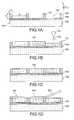
- FIGS. 1A-1Hillustrate an exemplary method according to the invention.
- FIGS. 2A and 2Billustrate alternative embodiments.
- FIGS. 1A-1HAn exemplary method according to the invention, for making a device including one or more enclosures filled with at least one liquid and closed with at least one membrane, will now be given in connection with FIGS. 1A-1H .
- each cavity 120being laterally delimited by walls 110 formed in one or more thin layers, as well as at the bottom, by a layer of the support.
- the walls 110 of the cavities 120may be distributed so as to give the latter a shape in the plane of the substrate which may be according to several examples: circular, oval, square, rectangular, polygonal or star-shaped.
- the walls 110 separating the cavities 120ensure their mutual seal.
- the support 100may be transparent, and for example in the form of a glass slab or of a plastic material such as a polyethylene terephthalate (PET) layer.
- PETpolyethylene terephthalate
- the support 100may be formed with a substrate 102 , for example in glass, on which one or more thin layers are formed, for example at least one layer 104 of flexible material, based on polyethylene terephthalate (PET).
- PETpolyethylene terephthalate
- An intermediate adhesive layer, for example based on acrylate,may optionally be provided for having the layer 104 adhere to the substrate 102 .
- the cavities 120may be made, by depositing a layer 106 on the support 100 , and then by etching this layer 106 so as to delimit the locations of the walls 110 .
- the layer 106 in which the cavities 120 are definedmay for example be a layer of photosensitive resin.
- the making of the cavities 120may at least comprise one photolithographic step.
- the cavities 120may be formed with a method in which a layer 106 is formed on the support, and the locations of the cavities 120 are then made by stamping, with a mold provided with protruding patterns which are applied by pressing on the layer 106 .
- a layer 106 of polymeric materialmay be deposited on the substrate 102 and then this layer 106 may be locally etched through a mask, for example by RIE or high density plasma etching with a mixture of O 2 , with a fluorinated gas of the SF 6 and/or CHF 3 type.
- the layer 106may be formed by lamination on a substrate 102 of a polymeric material layer in which the cavities 120 have been made beforehand, for example by etching.
- the size and the localization of the walls 110depend on the intended application for the device.
- the walls 110may be formed according to a geometry intended for not bringing about any perturbation or bringing about negligible or non-visible perturbations, on the path of the light rays crossing the support 100 .
- the walls 110may be formed on the basis of a transparent resin and in which patterns may be made by photolithography, for example a resin based on ORMOCER®, for example as described in document: ⁇ ORMOCER® for Optical Interconnection Technology>>, R. Buestrich, F. Kahlenberg, M. Popall et al., Journal of Sol-Gel Science and Technology 20, 181-186, 2001.
- the walls 110 separating the cavities 120may have a thickness e defined in a direction parallel to the main plane of the substrate or support (defined in FIG. 1A in a plane parallel to the plane [O; ⁇ right arrow over (i) ⁇ ; ⁇ right arrow over (j) ⁇ ] of an orthogonal reference system [O; ⁇ right arrow over (i) ⁇ ; ⁇ right arrow over (j) ⁇ ; ⁇ right arrow over (k) ⁇ ] defined in FIG. 1A ) for example comprised between 0.1 ⁇ m and 5 ⁇ m, or between 1 and 3 ⁇ m.
- the walls 110may also have a height H (H being defined in FIG. 1A in a direction parallel to the vector ⁇ right arrow over (k) ⁇ of the orthogonal reference system [O; ⁇ right arrow over (i) ⁇ ; ⁇ right arrow over (j) ⁇ ; ⁇ right arrow over (k) ⁇ ] comprised for example between 5 and 50 ⁇ m, or between 10 and 30 ⁇ m.
- Hbeing defined in FIG. 1A in a direction parallel to the vector ⁇ right arrow over (k) ⁇ of the orthogonal reference system [O; ⁇ right arrow over (i) ⁇ ; ⁇ right arrow over (j) ⁇ ; ⁇ right arrow over (k) ⁇ ] comprised for example between 5 and 50 ⁇ m, or between 10 and 30 ⁇ m.
- the cavities 120may also have a diameter or a side or a length D (defined in a direction parallel to the plane [O; ⁇ right arrow over (i) ⁇ ; ⁇ right arrow over (j) ⁇ ] of the orthogonal reference system [O; ⁇ right arrow over (i) ⁇ ; ⁇ right arrow over (j) ⁇ ; ⁇ right arrow over (k) ⁇ ] comprised for example between 5 ⁇ m and 500 ⁇ m or between 50 ⁇ m and 300 ⁇ m.
- Ddefined in a direction parallel to the plane [O; ⁇ right arrow over (i) ⁇ ; ⁇ right arrow over (j) ⁇ ] of the orthogonal reference system [O; ⁇ right arrow over (i) ⁇ ; ⁇ right arrow over (j) ⁇ ; ⁇ right arrow over (k) ⁇ ] comprised for example between 5 ⁇ m and 500 ⁇ m or between 50 ⁇ m and 300 ⁇ m.
- the given materialmay be a liquid, a so-called ⁇ functional liquid>>, i.e. selected for specific properties, for example such as refractive index, light absorption capacity, polarization, response to electric or light stimuli.
- the given liquid materialmay for example be 1-butyl-3-methylimidazolium acetate capable of being solidified at a temperature of the order of ⁇ 20° C.
- the given materialmay be paraffin oil of the Nujol® type from Plough capable of being solidified at a temperature of the order of ⁇ 40° C.
- the given materialmay be a mixture of 2,3-bis-n-decyloxyanthracene (DDOA) in 1-octanol, capable of being gelled or transformed into the form of a gel at a temperature comprised between 20 and 40° C.
- DDOA2,3-bis-n-decyloxyanthracene
- gelis meant a body stemming from the solidification of colloidal substances or else a continuous solid lattice surrounding a continuous liquid phase.
- the fillingmay be carried out by a piece of equipment E aiming at the inside of the cavities 120 and projecting the liquid material 130 as a jet or as drops 132 , with a volume which may be of the order of several picoliters.
- the liquidmay be delivered with a technique adapted to localization of small volumes, i.e. several picoliters to several hundred picoliters.
- the piece of equipment E usedmay apply a technique for dispensing liquid similar to the one for dispensing with an ink jet.
- the liquid material 130may partly or completely fill the cavities. A total filling of the cavities may be carried out so as to attain the top 112 of the walls 110 or to slightly jut out above the top 112 of the walls 110 .
- one or several cavities 120may be filled with a mixture of several liquids in proportions adjusted according to the targeted application.
- a mixture of several liquidsin proportions adjusted according to the targeted application.
- the lattermay be provided for delivering at least one active ingredient.
- the filling of the cavitiesmay be carried out with a liquid including active molecules and a solvent.
- the concentration or the dosage of the active moleculesmay differ according to the cavities 120 .
- a gradation of the active ingredient concentration between the cavities of the devicemay thus be provided.
- the active ingredientmay be a substance which enters the composition of a drug and which is responsible for the pharmacodynamic or therapeutic properties of the latter.
- several cavities 120may also be filled with liquids 130 , 134 , 136 different from one cavity to the other. This may notably be applied for an optical application of the device, when it is sought to impart to the cavities, optical properties different from each other.
- a different volume of liquidmay be provided from one cavity to the other.
- the liquid material 130may include organic solvent(s).
- the solvent usedmay be the glycol ether Dowanol TPM (tri-propylene glycol methyl ether).
- Solidificationmay be partial so that at least the upper portion of the liquid material 130 or of the liquid present in the cavities is transformed into the solid state, or may be complete.
- the liquidmay be brought to a temperature at least lower than or equal to the one at which the saturation pressure of the liquid material 130 present in the cavities 120 is attained or, when several liquids are present, to the one at which the smallest saturation pressure value of the liquid present in the cavities 120 is attained.
- the liquid material 130 filling the cavitiesis 1-butyl-3-methylimidazolium acetate
- the liquidmay be brought to a temperature below ⁇ 20° C. in order to carry out this solidification.
- the liquidmay be brought to a temperature below ⁇ 40° C. in order to carry out this solidification.
- the solidification stepmay be replaced with a step for transforming the given filling material into a gel.
- the given material for filling the cavitiesis a material capable of being transformed into a gel or formed with a mixture including a gelling component.
- An exemplary mixturemay be formed with 2,3-bis-n-decyloxyanthracene (DDOA) in 1-octanol.
- DDOA2,3-bis-n-decyloxyanthracene
- the appearance of the gelmay occur, depending on the aforementioned mixture used, between 20 and 40° C.
- a subsequent deposition of a membrane for closing the cavitiesmay thus be achieved at room temperature.
- return to the liquid state of the gel for filling the cavities 120may be carried out at a temperature above this temperature of 40° C.
- the cooling stepmay be carried out in a deposition chamber in which a closure layer is intended to be subsequently made in the form of a membrane, which may be elastic or flexible.
- a system for cooling the deviceis provided in the deposition chamber.
- a systemmay for example comprise a platinum and Peltier effect module or a sample holder with a system for circulating liquid nitrogen.
- a technique for cooling the rear of the support 100 with helium or a heat transfer gasmay also be applied.
- Coolingmay also be provided by an enclosure with circulation of a heat transfer fluid, the deposition chamber being pressurized with a neutral gas toward the liquid 130 .
- a vacuum pumping systemmay also be provided in the deposition chamber in order to avoid condensation phenomena.
- the support 100may be placed at room temperature in the deposition chamber, a dry and neutral gas toward the liquid being first of all introduced at a pressure which is close to ambient pressure. In order to carry out solidification, cooling is then performed in order to attain the desired solidification, which may be partial or at the surface or complete.
- the deposition chambermay be brought to a temperature of the order of ⁇ 20° C. or ⁇ 30° C.
- a temperature located in such a rangeallows solidification of standard ionic liquids such as for example 1-butyl-3-methylimidazolium acetate, 1-butyl-3-methylimidazolium methylsulfate or 1-butyl-3-methylimidazolium thiocyanate.
- standard ionic liquidssuch as for example 1-butyl-3-methylimidazolium acetate, 1-butyl-3-methylimidazolium methylsulfate or 1-butyl-3-methylimidazolium thiocyanate.
- the given material located in the cavitiesis in the form of a solid 140 or is solid at the surface.
- FIGS. 1D and 1Edeposition of a closure layer 150 is carried out on the top 112 of the walls 110 and on the surface of the given material 140 , solidified or transformed into a gel.
- the closure layer 150is provided as a flexible membrane which may be based on an elastic material and allows formation of closed cavities or closed enclosures filled with liquids. With this closure layer or membrane, the seal of the cavities may be ensured.
- the membraneis notably provided for making a barrier to humidity, to acids and to solvents and optionally an electrically insulating layer.
- the material 152 of the closure layer 150may be poly-para-xylylene also known as Parylene®. Such a material polymerizes at room temperature, and may be suitably formed so as to conform to the shape of the surface on which it is deposited.
- the thickness of the deposited materialmay be uniform and comprised, according to the applications, between several nanometers and several micrometers, for example between about hundred nanometers and several tens of microns, for example between 0.2 ⁇ m and 5 ⁇ m.
- parylenewith view to closure has the benefit of giving the possibility of obtaining a continuous, compliant, colorless and transparent film of small thickness, as well as good protection properties, parylene being impervious, resistant to aggressive environments, to solvents and to gases.
- the depositionmay be carried out in the gas phase, for example with CVD (Chemical Vapor Deposition) deposition.
- CVDChemical Vapor Deposition
- Deposition of the material 152 of the closured layer 150may be carried out under a pressure comprised between 1 and 500 mbars, or in a primary vacuum. At such a pressure, the filling liquids usually tend to evaporate. In the present case, as the liquid(s) 130 filling the cavities 120 have been at least partly solidified or transformed into a gel, evaporation phenomena do not occur.
- the formation of the parylene layermay be accomplished under standard conditions, pyrolysis of di-para-xylylene is carried out beforehand at 680° C., and then polymerization of the para-xylylene monomer at the surface of the sample is carried out at a temperature allowing the given material to be maintained in the solid state.
- the given solidified materialis for example butyl-3-methylimidazolium acetate, 1-butyl-3-methylimidazolium methylsulfate or 1-butyl-3-methylimidazolium thiocyanate
- the depositionmay be carried out at a temperature comprised between ⁇ 30° C. and ⁇ 20° C., when the given solidified material may be maintained in the solid state.
- a vacuummay be provided in the deposition chamber.
- the temperature of the deposition chamberis again increased in order to bring back the solidified material 140 to the liquid state 130 .
- the temperature around the devicemay for example be brought back to room temperature.
- closed cavities 120 filled with liquidare formed.
- a device including several liquid enclosures each partly closed by an elastic material membrane and by the walls 110 of a support 100was thereby made.
- One or more additional layers 160may be formed above the closure layer 150 ( FIG. 1H ). One or more additional layers 160 may be made. In order to make such (an) additional layer(s), deposition or transfer may for example be carried out by lamination.
- the additional layermay be a film of elastic material which may for example be identical with the layer 104 , for example based on PET.
- the layer 160may then be covered with one or more functional layers (schematized by a block referenced as 170 ) for example having antireflection properties, or hard varnish, antifouling or antiabrasion or shockproof properties.
- one or more functional layers(schematized by a block referenced as 170 ) for example having antireflection properties, or hard varnish, antifouling or antiabrasion or shockproof properties.
- the substrate 102may, as for it, be kept or, according to an alternative, separated from the flexible material layer 104 .
- separation of the closed cavities 120 from each othermay be carried out.
- the closed enclosures filled with liquidare thus dissociated or individualized.
- Such a separationmay for example be made with a laser, or with ultrasonic waves or with at least one cutting tool.
- the method which has just been givenmay be adapted to the deposition of materials other than parylene for example a transparent material such as poly(1,3,5-trivinyltrimethylcyclotrisiloxane(designated as poly(V3D3)), which may be deposited by iCVD (initiated CVD), as this is described in the article Biomacromolecules, 2007, 8, 2564-2570.
- the deposition temperaturemay be of the order of 35° C. for a deposition pressure comprised between 350 and 450 mTorrs. Such a pressure and such a temperature may possibly allow the use of a large range of possible liquids for the material given for filling the cavities 120 .
- Poly(1,3,5)trivinyltrimethylcyclotrisiloxane(designated as poly(V3D3)) may be deposited at a pressure and a temperature at which the given material 130 initially as a liquid may be maintained in solidified form, and is capable of returning to a liquid state at ambient pressure and temperature.
- the method according to the inventionmay be used for making optical lenses, or matrices of lenses.
- said closure layermay be a parylene layer formed as described earlier, by deposition on a material which has been solidified beforehand or transformed into a gel, and may then be brought back to the liquid state after deposition so as to form said liquid of said enclosure.
Landscapes
- Physics & Mathematics (AREA)
- General Physics & Mathematics (AREA)
- Optics & Photonics (AREA)
- Chemical & Material Sciences (AREA)
- Chemical Kinetics & Catalysis (AREA)
- Engineering & Computer Science (AREA)
- Manufacturing & Machinery (AREA)
- Micromachines (AREA)
- Ink Jet (AREA)
- Application Of Or Painting With Fluid Materials (AREA)
- Electrochromic Elements, Electrophoresis, Or Variable Reflection Or Absorption Elements (AREA)
- Physical Or Chemical Processes And Apparatus (AREA)
Abstract
Description
Claims (20)
Applications Claiming Priority (3)
| Application Number | Priority Date | Filing Date | Title |
|---|---|---|---|
| FR0854335AFR2933205B1 (en) | 2008-06-27 | 2008-06-27 | IMPROVED METHOD FOR MAKING LIQUID-FILLED ENCLOSURES AND CLOSED BY A MEMBRANE |
| FR0854335 | 2008-06-27 | ||
| PCT/EP2009/057870WO2010003821A2 (en) | 2008-06-27 | 2009-06-24 | Improved method for making enclosures filled with liquid and sealed by a membrane |
Publications (2)
| Publication Number | Publication Date |
|---|---|
| US20110180944A1 US20110180944A1 (en) | 2011-07-28 |
| US8477406B2true US8477406B2 (en) | 2013-07-02 |
Family
ID=40373532
Family Applications (1)
| Application Number | Title | Priority Date | Filing Date |
|---|---|---|---|
| US13/001,615Expired - Fee RelatedUS8477406B2 (en) | 2008-06-27 | 2009-06-24 | Method for making enclosures filled with liquid and closed by a membrane |
Country Status (7)
| Country | Link |
|---|---|
| US (1) | US8477406B2 (en) |
| EP (1) | EP2297599B1 (en) |
| JP (1) | JP5547180B2 (en) |
| KR (1) | KR101604012B1 (en) |
| CN (1) | CN102089679B (en) |
| FR (1) | FR2933205B1 (en) |
| WO (1) | WO2010003821A2 (en) |
Families Citing this family (8)
| Publication number | Priority date | Publication date | Assignee | Title |
|---|---|---|---|---|
| JP3360843B2 (en) | 1992-07-09 | 2003-01-07 | ヤクモ株式会社 | Soundproof panel assembling method using pillars for assembling soundproof panels in prefabricated soundproof building |
| FR2897164B1 (en) | 2006-02-09 | 2008-03-14 | Commissariat Energie Atomique | REALIZING CAVITIES THAT CAN BE FILLED BY A FLUID MATERIAL IN AN OPTICAL MICROTECHNOLOGICAL COMPOUND |
| FR2929715B1 (en) | 2008-04-04 | 2010-09-10 | Commissariat Energie Atomique | METHOD FOR PRODUCING MICRONIC OR SUBMICRONIC CAVITIES |
| FR2933205B1 (en) | 2008-06-27 | 2010-08-13 | Commissariat Energie Atomique | IMPROVED METHOD FOR MAKING LIQUID-FILLED ENCLOSURES AND CLOSED BY A MEMBRANE |
| FR2963112B1 (en) | 2010-07-21 | 2013-02-15 | Commissariat Energie Atomique | WALL MICROSTRUCTURE WITH DETERMINED OPTICAL PROPERTIES AND METHOD FOR PRODUCING MICROSTRUCTURES |
| CN105223635B (en)* | 2015-10-21 | 2017-03-22 | 苏州大学 | Method for designing and manufacturing aspheric liquid lens by using non-uniform film |
| FR3120561B1 (en)* | 2021-03-12 | 2023-02-10 | Addup | Method for cutting a part comprising a plurality of fine elements separated by interstices |
| CN114777699A (en)* | 2022-03-11 | 2022-07-22 | 江苏林谷智能科技有限公司 | Large space positioning and calibrating device and algorithm for fire fighting system |
Citations (43)
| Publication number | Priority date | Publication date | Assignee | Title |
|---|---|---|---|---|
| US3863249A (en) | 1973-07-30 | 1975-01-28 | Motorola Inc | Magnetic fluid display device |
| US3978580A (en) | 1973-06-28 | 1976-09-07 | Hughes Aircraft Company | Method of fabricating a liquid crystal display |
| CH591090A5 (en) | 1976-03-29 | 1977-09-15 | Wenger Jean Sebastien | Thin-edged lens for focussing solar rays in heater - with liquid-filled transparent or translucent shell |
| US4989226A (en) | 1987-08-21 | 1991-01-29 | Brigham Young University | Layered devices having surface curvature |
| US5417801A (en) | 1993-06-29 | 1995-05-23 | Xerox Corporation | Process to manufacture bushings for micromechanical elements |
| EP0782037A1 (en) | 1995-12-30 | 1997-07-02 | Samsung Display Devices Co., Ltd. | LCD Device with improved resilient adhesive spacers |
| WO1999045143A2 (en) | 1998-03-06 | 1999-09-10 | Novo Nordisk A/S | A fluorescence polarization screening method |
| EP0977076A2 (en) | 1998-07-31 | 2000-02-02 | Canon Kabushiki Kaisha | Color filter, production process of color filter, liquid crystal display device using the color filter, and production process of black matrix |
| US6063653A (en) | 1998-07-07 | 2000-05-16 | Industrial Technology Research Institute | Method of fabricating a TFT-LCD |
| WO2002065215A2 (en) | 2001-02-15 | 2002-08-22 | Sipix Imaging, Inc. | Process for roll-to-roll manufacture of a display by synchronized photolithographic exposure on a substrate web |
| WO2002088671A1 (en) | 2001-04-26 | 2002-11-07 | Esytech Ab | A separation unit, a method for separation, and a device for mounting a separation unit in a separation apparatus |
| JP2002323630A (en) | 2001-04-25 | 2002-11-08 | Ntt Advanced Technology Corp | Method and apparatus for manufacturing optical circuit by liquid ejector |
| US6525865B2 (en)* | 2000-05-30 | 2003-02-25 | Seiko Epson Corporation | Electrophoretic display and method for producing same |
| WO2003021346A1 (en) | 2001-08-28 | 2003-03-13 | Sipix Imaging, Inc. | Electrophoretic display device with sub relief structure |
| US20030076609A1 (en) | 2001-10-02 | 2003-04-24 | Seiko Epson Corporation | Color filter and manufacturing method therefor, display device and electronic equipment |
| US20040029303A1 (en) | 2002-08-07 | 2004-02-12 | Hart Mark Whitney | Discrete nano-textured structures in biomolecular arrays, and method of use |
| US20040161201A1 (en) | 2002-12-09 | 2004-08-19 | Jean-Charles Souriau | Optical arrangement with two optical inputs/outputs and production methods |
| US20040165252A1 (en) | 2000-03-03 | 2004-08-26 | Rong-Chang Liang | Electrophoretic display and novel process for its manufacture |
| US6947202B2 (en) | 2000-03-03 | 2005-09-20 | Sipix Imaging, Inc. | Electrophoretic display with sub relief structure for high contrast ratio and improved shear and/or compression resistance |
| US6958207B1 (en) | 2002-12-07 | 2005-10-25 | Niyaz Khusnatdinov | Method for producing large area antireflective microtextured surfaces |
| US20050275072A1 (en) | 2004-05-26 | 2005-12-15 | Haluzak Charles C | Package having bond-sealed underbump |
| FR2872589A1 (en) | 2004-07-02 | 2006-01-06 | Essilor Int | Transparent optical unit e.g. ophthalmic lens, producing method, involves cutting optical component along defined contour on its surface related to determined shape for optical unit, and drilling component to fix optical unit on support |
| US20060006336A1 (en) | 2004-07-02 | 2006-01-12 | Essilor International | Process for producing a transparent optical element, optical component involved in this process and optical element thus obtained |
| WO2006052763A2 (en) | 2004-11-04 | 2006-05-18 | Microchips, Inc. | Compression and cold weld sealing methods and devices |
| EP1672394A1 (en) | 2004-12-16 | 2006-06-21 | Ecole d'Ingénieurs ARC | Method for producing a device having a plastic membrane and device so manufactured |
| FR2879757A1 (en) | 2004-12-17 | 2006-06-23 | Essilor Int | METHOD FOR PRODUCING A TRANSPARENT OPTICAL ELEMENT, OPTICAL COMPONENT INVOLVED IN THIS METHOD AND OPTICAL ELEMENT THUS OBTAINED |
| WO2006067650A1 (en) | 2004-12-20 | 2006-06-29 | Koninklijke Philips Electronics N.V. | Method of manufacturing an electrophoretic display device and electrophoretic display device |
| WO2006116616A2 (en) | 2005-04-26 | 2006-11-02 | Applera Corporation | Systems and methods for multiple analyte detection |
| US7136216B1 (en) | 2005-12-15 | 2006-11-14 | Palo Alto Research Center Incorporated | Dual-stage tape-sealing of microcells or channels for display applications |
| EP1722424A1 (en) | 2005-05-13 | 2006-11-15 | Université Libre de Bruxelles | Method for the manufacturing of homeotropically aligned layer of discotic liquid crystals |
| US20060275711A1 (en) | 2005-06-07 | 2006-12-07 | Chien-Chung Fu | Method of manufacturing a LIGA mold by backside exposure |
| FR2888948A1 (en) | 2005-07-20 | 2007-01-26 | Essilor Int | PIXELLIZED TRANSPARENT OPTIC COMPONENT COMPRISING AN ABSORBENT COATING, METHOD FOR PRODUCING THE SAME AND USE THEREOF IN AN OPTICAL ELEMENT |
| FR2888953A1 (en) | 2005-07-20 | 2007-01-26 | Essilor Int | PIXELLIZED OPTIC COMPONENT WITH APODIZED WALLS, METHOD FOR MANUFACTURING THE SAME AND USE THEREOF IN THE MANUFACTURE OF A TRANSPARENT OPTICAL ELEMENT |
| US20070029277A1 (en) | 2005-08-02 | 2007-02-08 | International Business Machines Corporation | Injection molded microoptics |
| EP1791197A2 (en) | 2005-11-25 | 2007-05-30 | Seiko Epson Corporation | Electrochemical cell structure and method of fabrication |
| FR2897164A1 (en) | 2006-02-09 | 2007-08-10 | Commissariat Energie Atomique | REALIZING CAVITIES THAT CAN BE FILLED BY A FLUID MATERIAL IN AN OPTICAL MICROTECHNOLOGICAL COMPOUND |
| GB2435717A (en) | 2003-09-04 | 2007-09-05 | Hitachi Ltd | Organic active matrix display device |
| WO2007141525A1 (en) | 2006-06-07 | 2007-12-13 | University Of Strathclyde | Multistable reflective liquid crystal device |
| US20080037104A1 (en) | 2005-02-23 | 2008-02-14 | Pixtronix, Inc. | Alignment methods in fluid-filled MEMS displays |
| US7374634B2 (en)* | 2004-05-12 | 2008-05-20 | Sipix Imaging, Inc. | Process for the manufacture of electrophoretic displays |
| US20080123045A1 (en) | 2004-08-31 | 2008-05-29 | Industrial Technology Research Institute | Manufacturing method for a transflective liquid crystal display device |
| WO2010003821A2 (en) | 2008-06-27 | 2010-01-14 | Commissariat A L'energie Atomique | Improved method for making enclosures filled with liquid and sealed by a membrane |
| US20100014036A1 (en) | 2008-07-15 | 2010-01-21 | Commissariat A L'energie Atomique | Alignment layer of liquid crystals deposited and rubbed before making microstructures |
Family Cites Families (2)
| Publication number | Priority date | Publication date | Assignee | Title |
|---|---|---|---|---|
| CN100543520C (en)* | 2006-07-20 | 2009-09-23 | 财团法人工业技术研究院 | Flexible photoelectric film and manufacturing method thereof |
| FR2907922B1 (en)* | 2006-10-30 | 2009-02-13 | Essilor Int | PROCESS FOR MANUFACTURING A SERIES OF OPHTHALMIC GLASSES AND FILM SHEET USED IN SUCH A METHOD. |
- 2008
- 2008-06-27FRFR0854335Apatent/FR2933205B1/ennot_activeExpired - Fee Related
- 2009
- 2009-06-24WOPCT/EP2009/057870patent/WO2010003821A2/enactiveApplication Filing
- 2009-06-24KRKR1020107029882Apatent/KR101604012B1/ennot_activeExpired - Fee Related
- 2009-06-24JPJP2011515366Apatent/JP5547180B2/ennot_activeExpired - Fee Related
- 2009-06-24CNCN2009801244034Apatent/CN102089679B/ennot_activeExpired - Fee Related
- 2009-06-24EPEP09779917.5Apatent/EP2297599B1/ennot_activeNot-in-force
- 2009-06-24USUS13/001,615patent/US8477406B2/ennot_activeExpired - Fee Related
Patent Citations (51)
| Publication number | Priority date | Publication date | Assignee | Title |
|---|---|---|---|---|
| US3978580A (en) | 1973-06-28 | 1976-09-07 | Hughes Aircraft Company | Method of fabricating a liquid crystal display |
| US3863249A (en) | 1973-07-30 | 1975-01-28 | Motorola Inc | Magnetic fluid display device |
| CH591090A5 (en) | 1976-03-29 | 1977-09-15 | Wenger Jean Sebastien | Thin-edged lens for focussing solar rays in heater - with liquid-filled transparent or translucent shell |
| US4989226A (en) | 1987-08-21 | 1991-01-29 | Brigham Young University | Layered devices having surface curvature |
| US5417801A (en) | 1993-06-29 | 1995-05-23 | Xerox Corporation | Process to manufacture bushings for micromechanical elements |
| EP0782037A1 (en) | 1995-12-30 | 1997-07-02 | Samsung Display Devices Co., Ltd. | LCD Device with improved resilient adhesive spacers |
| US5838414A (en) | 1995-12-30 | 1998-11-17 | Samsung Display Devices Co., Ltd. | LCD device with improved resilient adhesive spacers |
| WO1999045143A2 (en) | 1998-03-06 | 1999-09-10 | Novo Nordisk A/S | A fluorescence polarization screening method |
| US6063653A (en) | 1998-07-07 | 2000-05-16 | Industrial Technology Research Institute | Method of fabricating a TFT-LCD |
| EP0977076A2 (en) | 1998-07-31 | 2000-02-02 | Canon Kabushiki Kaisha | Color filter, production process of color filter, liquid crystal display device using the color filter, and production process of black matrix |
| US20040165252A1 (en) | 2000-03-03 | 2004-08-26 | Rong-Chang Liang | Electrophoretic display and novel process for its manufacture |
| US6947202B2 (en) | 2000-03-03 | 2005-09-20 | Sipix Imaging, Inc. | Electrophoretic display with sub relief structure for high contrast ratio and improved shear and/or compression resistance |
| US6525865B2 (en)* | 2000-05-30 | 2003-02-25 | Seiko Epson Corporation | Electrophoretic display and method for producing same |
| WO2002065215A2 (en) | 2001-02-15 | 2002-08-22 | Sipix Imaging, Inc. | Process for roll-to-roll manufacture of a display by synchronized photolithographic exposure on a substrate web |
| JP2002323630A (en) | 2001-04-25 | 2002-11-08 | Ntt Advanced Technology Corp | Method and apparatus for manufacturing optical circuit by liquid ejector |
| WO2002088671A1 (en) | 2001-04-26 | 2002-11-07 | Esytech Ab | A separation unit, a method for separation, and a device for mounting a separation unit in a separation apparatus |
| WO2003021346A1 (en) | 2001-08-28 | 2003-03-13 | Sipix Imaging, Inc. | Electrophoretic display device with sub relief structure |
| US20030076609A1 (en) | 2001-10-02 | 2003-04-24 | Seiko Epson Corporation | Color filter and manufacturing method therefor, display device and electronic equipment |
| US20040029303A1 (en) | 2002-08-07 | 2004-02-12 | Hart Mark Whitney | Discrete nano-textured structures in biomolecular arrays, and method of use |
| US6958207B1 (en) | 2002-12-07 | 2005-10-25 | Niyaz Khusnatdinov | Method for producing large area antireflective microtextured surfaces |
| US20040161201A1 (en) | 2002-12-09 | 2004-08-19 | Jean-Charles Souriau | Optical arrangement with two optical inputs/outputs and production methods |
| GB2435717A (en) | 2003-09-04 | 2007-09-05 | Hitachi Ltd | Organic active matrix display device |
| US7374634B2 (en)* | 2004-05-12 | 2008-05-20 | Sipix Imaging, Inc. | Process for the manufacture of electrophoretic displays |
| US20050275072A1 (en) | 2004-05-26 | 2005-12-15 | Haluzak Charles C | Package having bond-sealed underbump |
| FR2872589A1 (en) | 2004-07-02 | 2006-01-06 | Essilor Int | Transparent optical unit e.g. ophthalmic lens, producing method, involves cutting optical component along defined contour on its surface related to determined shape for optical unit, and drilling component to fix optical unit on support |
| US20060006336A1 (en) | 2004-07-02 | 2006-01-12 | Essilor International | Process for producing a transparent optical element, optical component involved in this process and optical element thus obtained |
| US20080123045A1 (en) | 2004-08-31 | 2008-05-29 | Industrial Technology Research Institute | Manufacturing method for a transflective liquid crystal display device |
| WO2006052763A2 (en) | 2004-11-04 | 2006-05-18 | Microchips, Inc. | Compression and cold weld sealing methods and devices |
| US20090246546A1 (en) | 2004-12-16 | 2009-10-01 | Herbert Keppner | Method for producing a plastic membrane device and the thus obtained device |
| EP1672394A1 (en) | 2004-12-16 | 2006-06-21 | Ecole d'Ingénieurs ARC | Method for producing a device having a plastic membrane and device so manufactured |
| WO2006067309A1 (en) | 2004-12-17 | 2006-06-29 | Essilor International (Compagnie Generale D'optique) | Method for making a transparent optical element, optical component used in said method and resulting optical element |
| US20090316110A1 (en) | 2004-12-17 | 2009-12-24 | Essilor International (Compagnie Gerale D'optique) | Method for making a transparent optical element, optical component used in said method and resulting optical element |
| FR2879757A1 (en) | 2004-12-17 | 2006-06-23 | Essilor Int | METHOD FOR PRODUCING A TRANSPARENT OPTICAL ELEMENT, OPTICAL COMPONENT INVOLVED IN THIS METHOD AND OPTICAL ELEMENT THUS OBTAINED |
| WO2006067650A1 (en) | 2004-12-20 | 2006-06-29 | Koninklijke Philips Electronics N.V. | Method of manufacturing an electrophoretic display device and electrophoretic display device |
| US20080037104A1 (en) | 2005-02-23 | 2008-02-14 | Pixtronix, Inc. | Alignment methods in fluid-filled MEMS displays |
| WO2006116616A2 (en) | 2005-04-26 | 2006-11-02 | Applera Corporation | Systems and methods for multiple analyte detection |
| EP1722424A1 (en) | 2005-05-13 | 2006-11-15 | Université Libre de Bruxelles | Method for the manufacturing of homeotropically aligned layer of discotic liquid crystals |
| US20060275711A1 (en) | 2005-06-07 | 2006-12-07 | Chien-Chung Fu | Method of manufacturing a LIGA mold by backside exposure |
| FR2888948A1 (en) | 2005-07-20 | 2007-01-26 | Essilor Int | PIXELLIZED TRANSPARENT OPTIC COMPONENT COMPRISING AN ABSORBENT COATING, METHOD FOR PRODUCING THE SAME AND USE THEREOF IN AN OPTICAL ELEMENT |
| US20080212023A1 (en) | 2005-07-20 | 2008-09-04 | Essilor International (Compagnie Generale D'optique) | Pixellized Optical Component with Apodized Walls, Method for Making Same and Use thereof in Making a Transparent Optical Element |
| US20080212017A1 (en) | 2005-07-20 | 2008-09-04 | Essilor International (Compagnie Generale D'optique) | Pixellized Transparent Optical Component Comprising an Absorbing Coating, Production Method Thereof and Use Thereof in an Optical Element |
| FR2888953A1 (en) | 2005-07-20 | 2007-01-26 | Essilor Int | PIXELLIZED OPTIC COMPONENT WITH APODIZED WALLS, METHOD FOR MANUFACTURING THE SAME AND USE THEREOF IN THE MANUFACTURE OF A TRANSPARENT OPTICAL ELEMENT |
| US20070029277A1 (en) | 2005-08-02 | 2007-02-08 | International Business Machines Corporation | Injection molded microoptics |
| EP1791197A2 (en) | 2005-11-25 | 2007-05-30 | Seiko Epson Corporation | Electrochemical cell structure and method of fabrication |
| US7136216B1 (en) | 2005-12-15 | 2006-11-14 | Palo Alto Research Center Incorporated | Dual-stage tape-sealing of microcells or channels for display applications |
| WO2007090828A1 (en) | 2006-02-09 | 2007-08-16 | Commissariat A L'energie Atomique | Production of cavities that can be filled with a fluid material in an optical microtechnological component |
| FR2897164A1 (en) | 2006-02-09 | 2007-08-10 | Commissariat Energie Atomique | REALIZING CAVITIES THAT CAN BE FILLED BY A FLUID MATERIAL IN AN OPTICAL MICROTECHNOLOGICAL COMPOUND |
| US20090027767A1 (en) | 2006-02-09 | 2009-01-29 | Commissariat A L'energie Atomique | Production of cavities that can be filled with a fluid material in an optical microtechnological component |
| WO2007141525A1 (en) | 2006-06-07 | 2007-12-13 | University Of Strathclyde | Multistable reflective liquid crystal device |
| WO2010003821A2 (en) | 2008-06-27 | 2010-01-14 | Commissariat A L'energie Atomique | Improved method for making enclosures filled with liquid and sealed by a membrane |
| US20100014036A1 (en) | 2008-07-15 | 2010-01-21 | Commissariat A L'energie Atomique | Alignment layer of liquid crystals deposited and rubbed before making microstructures |
Non-Patent Citations (9)
| Title |
|---|
| Chiung-Wen Kuo et al., Monolithic integration of well-ordered nanoporous structures in the microfluidic channels for bioseparation, Journal of Chromatography, Aug. 2007. |
| M. Trejo-Valdez et al., Aerosol-gel deposition of photocurable ORMOSIL films doped with a terbium complex, Optical Materials, 25, (2004) 179-184. |
| Matthieu Liger, et al., Robust Parylene-To-Silicon Mechanical Anchoring, MEMS-3, IEEE, Micro Electro Mechanical Systems, the Sixteenth Annual International Conference, Jan. 19-23, 2003, pp. 602-605. |
| NUNC: Tapes, Lids and Mats, Announcement Nunc International, Jan. 2006. |
| R. Buestrich et al., ORMOCERs for Optical Interconnection Technology, Journal of Sol-Gel Science & Technology, 20, 181-186, 2001. |
| S. Cheylan et al., Optical study of polymer infiltration into porous Si based structures, Proceedings of SPIEE, May 2007. |
| San Ming Yang, et al., Opal Circuits of Light-Planarized Microphotonic Crystal Chips, Advanced Functional Materials, 12, 425, 2002. |
| W.S. O'Shaughnessy et al., Stable Biopassive Insulation Synthesized by Initiated Chemical Vapor Deposition of . . . , Biomacromolecules, 2007, 8, pp. 2564-2570. |
| Y. Nishijima et al., Inverse silica opal photonic crystals for optical sensing applications, Optics Express, 15(20), I2979, 2007. |
Also Published As
| Publication number | Publication date |
|---|---|
| JP5547180B2 (en) | 2014-07-09 |
| CN102089679B (en) | 2013-09-18 |
| WO2010003821A3 (en) | 2010-03-04 |
| CN102089679A (en) | 2011-06-08 |
| KR20110044951A (en) | 2011-05-03 |
| KR101604012B1 (en) | 2016-03-16 |
| US20110180944A1 (en) | 2011-07-28 |
| FR2933205B1 (en) | 2010-08-13 |
| FR2933205A1 (en) | 2010-01-01 |
| EP2297599B1 (en) | 2014-05-14 |
| JP2011525997A (en) | 2011-09-29 |
| EP2297599A2 (en) | 2011-03-23 |
| WO2010003821A2 (en) | 2010-01-14 |
Similar Documents
| Publication | Publication Date | Title |
|---|---|---|
| US8477406B2 (en) | Method for making enclosures filled with liquid and closed by a membrane | |
| Alvarez et al. | A microtensiometer to probe the effect of radius of curvature on surfactant transport to a spherical interface | |
| CN101421642B (en) | Optical element and lens array | |
| CN100549735C (en) | Method for preparing a device made of a film of plastic material and device thus obtained | |
| Broesch et al. | From concave to convex: capillary bridges in slit pore geometry | |
| US7785533B2 (en) | Chip, device using the chip, and method of using the same | |
| TWI385029B (en) | Microfluidic system and method for creating an encapsulated droplet with a removable shell | |
| Yang et al. | Tunable and latchable liquid microlens with photopolymerizable components | |
| KR20080076931A (en) | Prevent solution flow in fluid focus lenses | |
| Khare et al. | Switching liquid morphologies on linear grooves | |
| CN110770028A (en) | Container for use in a stereolithography system | |
| US8192672B2 (en) | Method for producing a retention matrix comprising a functional liquid | |
| Monti et al. | Two-Photon Laser Microprinting of Highly Ordered Nanoporous Materials Based on Hexagonal Columnar Liquid Crystals | |
| Günther et al. | EWOD system designed for optical switching | |
| Olivieri et al. | Fabrication of polymer lenses and microlens array for lab-on-a-chip devices | |
| Van Toan et al. | Glass capillaries based on a glass reflow into nano-trench for controlling light transmission | |
| Wang et al. | Numerical and experimental investigation of bubble dynamics via electrowetting-on-dielectric (EWOD) | |
| Pan et al. | Actuating fluid–fluid interfaces for the reconfiguration of light | |
| JP2008046359A (en) | Optical material, optical element, optical device, and display method of optical element | |
| Challita et al. | A 3D printing method for droplet-based biomolecular materials | |
| US20160299265A1 (en) | Methods for fabricating optical lenses | |
| Park et al. | A planar liquid lens design based on electrowetting | |
| US20150219605A1 (en) | Method for Producing a Chromatography Analysis Column | |
| Grilli et al. | Interferometric characterization of pyroelectrically activated micro-arrays of liquid lenses in lithium niobate crystals | |
| Sarles et al. | Physical encapsulation and controlled assembly of lipid bilayers within flexible substrates |
Legal Events
| Date | Code | Title | Description |
|---|---|---|---|
| AS | Assignment | Owner name:COMMISSARIAT A L'ENERGIE ATOMIQUE ET AUX ENERGIES Free format text:ASSIGNMENT OF ASSIGNORS INTEREST;ASSIGNORS:CANO, JEAN-PAUL;SAUGEY, ANTHONY;CLERC, LAURENCE;REEL/FRAME:026129/0833 Effective date:20110401 Owner name:ESSILOR INTERNATIONAL (COMPAGNIE GENERALE D'OPTIQU Free format text:ASSIGNMENT OF ASSIGNORS INTEREST;ASSIGNORS:CANO, JEAN-PAUL;SAUGEY, ANTHONY;CLERC, LAURENCE;REEL/FRAME:026129/0833 Effective date:20110401 | |
| STCF | Information on status: patent grant | Free format text:PATENTED CASE | |
| FPAY | Fee payment | Year of fee payment:4 | |
| AS | Assignment | Owner name:ESSILOR INTERNATIONAL (COMPAGNIE GENERALE D'OPTIQU Free format text:ASSIGNMENT OF ASSIGNORS INTEREST;ASSIGNOR:COMMISSARIAT A L'ENERGIE ATOMIQUE ET AUX ENERGIES ALTERNATIVES;REEL/FRAME:043791/0871 Effective date:20170327 | |
| AS | Assignment | Owner name:ESSILOR INTERNATIONAL, FRANCE Free format text:ASSIGNMENT OF ASSIGNORS INTEREST;ASSIGNOR:ESSILOR INTERNATIONAL (COMPAGNIE GENERALE D'OPTIQUE);REEL/FRAME:045853/0275 Effective date:20171101 | |
| FEPP | Fee payment procedure | Free format text:MAINTENANCE FEE REMINDER MAILED (ORIGINAL EVENT CODE: REM.); ENTITY STATUS OF PATENT OWNER: LARGE ENTITY | |
| LAPS | Lapse for failure to pay maintenance fees | Free format text:PATENT EXPIRED FOR FAILURE TO PAY MAINTENANCE FEES (ORIGINAL EVENT CODE: EXP.); ENTITY STATUS OF PATENT OWNER: LARGE ENTITY | |
| STCH | Information on status: patent discontinuation | Free format text:PATENT EXPIRED DUE TO NONPAYMENT OF MAINTENANCE FEES UNDER 37 CFR 1.362 | |
| FP | Lapsed due to failure to pay maintenance fee | Effective date:20210702 |