US8476882B2 - Reference voltage based equivalent series resistance (ESR) emulation for constant on-time (COT) control of buck regulators - Google Patents
Reference voltage based equivalent series resistance (ESR) emulation for constant on-time (COT) control of buck regulatorsDownload PDFInfo
- Publication number
- US8476882B2 US8476882B2US12/895,555US89555510AUS8476882B2US 8476882 B2US8476882 B2US 8476882B2US 89555510 AUS89555510 AUS 89555510AUS 8476882 B2US8476882 B2US 8476882B2
- Authority
- US
- United States
- Prior art keywords
- reference voltage
- voltage
- integrated circuit
- circuitry
- pwm
- Prior art date
- Legal status (The legal status is an assumption and is not a legal conclusion. Google has not performed a legal analysis and makes no representation as to the accuracy of the status listed.)
- Active, expires
Links
Images


Classifications
- H—ELECTRICITY
- H02—GENERATION; CONVERSION OR DISTRIBUTION OF ELECTRIC POWER
- H02M—APPARATUS FOR CONVERSION BETWEEN AC AND AC, BETWEEN AC AND DC, OR BETWEEN DC AND DC, AND FOR USE WITH MAINS OR SIMILAR POWER SUPPLY SYSTEMS; CONVERSION OF DC OR AC INPUT POWER INTO SURGE OUTPUT POWER; CONTROL OR REGULATION THEREOF
- H02M3/00—Conversion of DC power input into DC power output
- H02M3/02—Conversion of DC power input into DC power output without intermediate conversion into AC
- H02M3/04—Conversion of DC power input into DC power output without intermediate conversion into AC by static converters
- H02M3/10—Conversion of DC power input into DC power output without intermediate conversion into AC by static converters using discharge tubes with control electrode or semiconductor devices with control electrode
- H02M3/145—Conversion of DC power input into DC power output without intermediate conversion into AC by static converters using discharge tubes with control electrode or semiconductor devices with control electrode using devices of a triode or transistor type requiring continuous application of a control signal
- H02M3/155—Conversion of DC power input into DC power output without intermediate conversion into AC by static converters using discharge tubes with control electrode or semiconductor devices with control electrode using devices of a triode or transistor type requiring continuous application of a control signal using semiconductor devices only
- H02M3/156—Conversion of DC power input into DC power output without intermediate conversion into AC by static converters using discharge tubes with control electrode or semiconductor devices with control electrode using devices of a triode or transistor type requiring continuous application of a control signal using semiconductor devices only with automatic control of output voltage or current, e.g. switching regulators
Definitions
- the present inventionrelates to the stabilization of Constant On-Time (COT) control buck regulators. More particularly, the present invention relates to the stabilization of COT control buck regulators that use a low Equivalent Series Resistance (ESR) output capacitor.
- COTConstant On-Time
- ESREquivalent Series Resistance
- Buck regulatorsare a type of DC/DC controller that are used to convert a DC voltage to another lower DC voltage.
- the buck regulator chipis connected to an external LC circuit that includes an inductor and an output capacitor.
- An external voltage dividerproduces a feedback voltage.
- Pulse Width Modulation (PWM) signal(s)are created by the buck regulator to control the switching of an input voltage into the LC circuit.
- the PWM signal(s)may be composed of, or used to create, control signals for high-side and low-side switches for power and ground into the LC circuit to produce the DC output voltage. The larger the duty cycle of the high side PWM signal, the greater the DC output voltage.
- the feedback voltageis compared to a constant reference voltage to adjust the PWM signal(s). If the feedback voltage, and thus the output voltage, is too low or high, the duty cycle of the high side PWM signal is increased or decreased.
- Ceramic capacitorshave a very low equivalent series resistance (ESR) and result in unstable operation with standard Constant On-Time (COT) control schemes.
- COT DC/DC controllersrely on the ESR of the output capacitor to stabilize the buck system.
- the ESR of the output capacitorhas dramatic phase correction effect and is capable of compensating for the phase lag of the buck regulator's LC circuit.
- COT DC/DC controllersWhen COT DC/DC controllers are used with low ESR ceramic capacitors, they have required either an additional resistor added in series with the output capacitor, a Resistor-Capacitor (RC) circuit feeding from the switch node to the feedback voltage, or a resistor in series with the inductor together with a RC circuit filter to stabilize the system.
- RCResistor-Capacitor
- the present inventionallows for the use of COT control in a buck regulator using a low ESR capacitor. It overcomes the drawbacks of prior systems while maintaining the fast transient response and stability of constant on-time control.
- a reference voltageis compared to the feedback voltage to create the PWM signal(s).
- the present inventionuses a reference voltage that varies within a PWM cycle. This allows for stability in the feedback of COT control for the buck regulator. In effect, a ripple is put on the reference voltage that allows the buck regulator to compensate for the phase lag induced on the feedback voltage by the external LC circuit.
- the reference voltage generating circuitryis switched based on features of the PWM cycle, such as T on , when the PWM signal goes high, and T off , when the PWM signal goes low.
- Systems of the present inventiondo not require sensing a ramp portion of the external inductor current.
- FIGS. 1A-1Eshow examples of inductor currents and output voltages of buck regulators.
- FIG. 2shows an example of a reference voltage circuit of one embodiment of the present invention.
- FIG. 3shows an exemplary application of a buck regulator chip.
- FIGS. 4A-4Cshow a reference voltage system of one embodiment of the present invention that uses a ramping voltage for the reference voltage within a portion of the Pulse Width Modulation (PWM) cycle to provide for stable Constant On-Time (COT) control.
- PWMPulse Width Modulation
- FIGS. 5A-5Cshows a reference voltage system of one embodiment of the present invention that uses a Resistor-Capacitor (RC) circuit to create a reference voltage within a PWM cycle to provide for stable COT control.
- RCResistor-Capacitor
- FIGS. 6A-6Cshows a reference voltage system of one embodiment of the present invention that switches between two voltages within a PWM cycle to provide for stable COT control.
- FIG. 7shows an additional embodiment where a block is used to adjust the peaks and valleys of the reference voltage signal based on a feedback voltage.
- the difficulty of stabilizing a COT controlled buck regulatoris due to the phase lag introduced by the LC network.
- the output voltagebecomes phase shifted sufficiently from the inductor current, the system becomes instable.
- FIG. 1Bshows the inherent phase lag between inductor current (I L ) and output voltage (V out ). To simplify the 2 nd order system of the LC system network, all V out waveforms in this description are shown as a 1 st order system with straight lines.
- the system regulation pointis set by the reference voltage (FB ref or V ref ).
- the feedback voltageis compared to the reference voltage within the buck regulator.
- V outit is possible for V out to be higher than FB ref *(R 1 +R 2 )/R 1 when the high side switch is turning OFF. Therefore, another high-side-switch-turn-on may occur immediately after the high side switch turns off.
- the systemwill thus jump into an instable double pulse or triple pulse mode (or more pulses dependant on the inductor, output capacitance value, ESR, input and output voltages, and minimum off-time) as shown in FIG. 1D .
- the output voltageis still regulated, but the voltage ripple is two times bigger than in a stable system.
- Other undesirable characteristics of this instable operationare: reduced transient performance, increased Electro-Magnetic Interference (EMI), and increased power loss.
- EMIElectro-Magnetic Interference
- Oscillator based voltage mode PWM controlhas at least two zeros to compensate for the phase lag.
- Oscillator based Current mode controlreduces the number of system poles by sensing a switch or an inductor current in order to simplify the compensation but at the expense of additional circuitry.
- COT control systemscan have an output capacitor with a sufficient ESR to dominate the output ripple so as to ensure system stability. Effectively, the ESR zero is at a low enough frequency to eliminate the phase lag caused by the LC network and guarantees the system stability as shown in FIGS. 1A and 1C .
- the present inventioncreates internal phase-lag compensation to stabilize the buck regulator system without requiring the use of a high ESR output capacitor.
- This phase-lagattempts to match the phase between the control loop and the phase lagged ripple voltage on the output.
- a PWM duty cycle dependent reference slopecan be generated to fulfill this task as shown in FIG. 1E .
- FB refcomes from a traditional band gap and is fixed during operation.
- FB refis a saw tooth waveform with its slope either proportional to duty cycle (D) for universal applications or fixed for a known phase lag system. This avoids turning on the high side control transistor during V out rising edge, and eliminates the possibility of double and multiple pulsing.
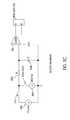
- an integrated circuitincludes a buck regulator 202 using Constant On-Time control.
- the buck regulator 202includes reference voltage generating circuitry 204 to produce a reference voltage value and comparison circuitry 206 to produce a PWM signal.
- high side and low side PWM signalsare created.
- the comparison circuitry 206receives the reference voltage from the reference voltage generating circuitry 204 and a feedback voltage from a feedback pin 208 of the integrated circuit 200 .
- the reference voltage generating circuitryproduces a reference voltage that varies within a PWM cycle and is adjusted based on features of the PWM cycle.
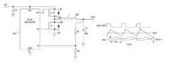
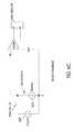
- FIG. 3shows an application for the buck converter 302 .
- an external LC circuitincluding an inductor 308 and output capacitor 306 creates a low pass filter used to produce the DC output voltage.
- a voltage divider including resistors R 1 and R 2is connected to the output voltage to create the feedback voltage for the feedback pin of the integrated circuit.
- the high-side switch 310 and the low-side switch 312are used to switch between the input voltages and ground into the LC circuit to produce the output voltage.
- the output capacitor 306is a ceramic capacitor with an ESR of less than 15 milli-ohms.
- the reference voltage generator circuitrystabilizes the constant on-time control even with the low ESR of a ceramic capacitor.
- FIGS. 4A-4C , FIGS. 5A-5C and FIGS. 6A-6Cshow different embodiments of a reference voltage generating circuit of the present invention.
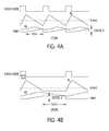
- FIGS. 4A-4Cshow a first embodiment of a reference voltage generating circuit using ramp voltage.
- the reference voltageis created by switching in a first voltage (775 mV) at time T on , when the PWM signal goes high.
- current source 404 with a ramp functionis used.
- FIG. 4Ashows a Continuous Condition Mode (CCM) example where the inductor current does not go to zero.
- FIG. 4Bshows a Discontinuous Conduction Mode (DCM) example where the inductor current does go to zero.
- CCMContinuous Condition Mode
- DCMDiscontinuous Conduction Mode
- the voltage source 406is switched into circuit to produce the reference voltage.
- the duty cycle signal D from the switching node, or the high side and low side control signal of the PWM signalcan also be used to derive the charging current.
- DCMDiscontinuous Conduction Mode
- the reference voltageis maintained at a lower value than the feedback ripple valley when the control switch is conducting, and then the reference voltage is ramped up during the off time, and crosses the feedback voltage at the target value. If the reference voltage crosses the feedback voltage higher or lower than the target, some correction circuitry may be used to compensate the slope of the valley voltage of the reference as embodied in FIG. 7 .
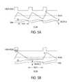
- FIGS. 5A-5Cshows a simplified control method using a reference voltage generating circuitry.
- first voltage source 502 and second voltage source 504are alternately switched into a RC circuit comprising resistor 506 and capacitor 508 to produce the reference voltage.
- the first voltage source 502is switched in when the PWM signal goes high and the second voltage source 504 is switched in when the PWM signal is low.
- FIGS. 5A-5Cuses a RC circuit delay to generate the phase shifted reference slope. Compared with the example of FIGS. 4A-4C , this control method is simpler and has no difference between CCM and DCM operation.
- This methodhas a fixed reference slope regardless the duty cycle of the buck regulator which means if the V out 's rising edge is much slower than the reference RC circuit slope's rising edge, the system may again jump into instable regulation. Therefore, this embodiment requires a longer minimum off time.
- Another drawback of this methodis an accuracy error of the system V out .
- the feedback voltagemight cross reference slope at different points during the RC circuit filter rising edge. The bigger the duty cycle, the larger the V out error will be. Therefore, compensation circuitry is needed if the buck regulator uses a high duty cycle.
- FIG. 6A-6Cis an even simpler method using reference voltage generating circuitry to switch between two constant voltages within the PWM cycle.
- voltage source 602 and voltage source 604are switched in and out as the reference voltage, V ref , without using a RC circuit.
- This methoduses half of the T off period for the reference voltage to get back to a target value.
- the disadvantage of this methodis that transient performance is a little slower than other methods; hence the output voltage overshoot is a little bit larger.
- FIGS. 4A-4C , FIGS. 5A-5C and FIGS. 6A-6Csolve the inherent instability in COT buck regulator systems with where low ESR of the output capacitor results in a heavily phase shifted output voltage. These control methods work equally well when using capacitors with higher ESR.
- the adjusting of the reference voltagerequires no direct sensing of the inductor current.
- the publication “Emulated Ripple Technique Advances Hysteric Switchmode Supplies”describes a prior system that operates in a current mode that requires sensing the external inductor current ramp current with the buck regulator chip.
- the current mode control scheme of this prior art systemcan be relatively complex and depending on the design, may require an additional pin to connect to the sensed current value.
- T off1the time when the inductor current is zeroed, can be used for DCM operation as described above, but the determination of T off1 does not require sensing the external inductor current.
- the T off1 valuecan be derived from chip internal control information.
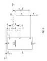
- FIG. 7shows an embodiment where the voltages of the peaks and valleys of the V ref signal (V ref4 ) at the comparator COMP 2 are adjusted using block 702 rather than the V ref signal merely switching between two fixed voltage values.
- V ref2 and V ref1define the peaks and valleys of the reference voltage signal (V ref4 ) at the comparator COMP 2 .
- V ref2 (and thus V ref1 )are set by the operation of the low pass filter (including the resister R 4 and capacitor C 4 ) and the transconductance amplifier GM 1 .
- a voltage error amplifiercan be used in the place of the transconductance amplifier GM 1 .
- the transconductance amplifier GM 1compares the voltage between the output VREF_SLOW of the low pass filter and the feedback signal FB, and generates a directional current IGM which is proportional to the difference between VREF_SLOW and FB. If FB ⁇ VREF_SLOW, then the current IGM flows out from the transconductance amplifier GM 1 , and voltage V x increases which in turn causes VREF_SLOW, V ref2 and V ref1 to increase. If FB>VREF_SLOW then the current IGM flows out into the transconductance amplifier GM 1 , and voltage V x decreases which in turn causes VREF_SLOW, Vref 2 and Vref 1 to decrease.
- block 702adjusts the average value of V ref4 at comparator COMP 2 and corrects for propagation delays and offsets at the comparator COMP 2 . This has the benefit of improving system regulation accuracy.
- TON_Bis a digital signal which can be Low or High. If TON_B is low then the GATE is low which turns on the external PMOS. If TON_B is low then TON is high and the switch SW 1 connects to V REF1 , and V REF4 will be discharged to V REF1 through R 8 . If TON_B is high then GATE is high which turns off the external PMOS. If TON_B is high then TON is low, the switch SW 2 connect to V REF2 , and V REF4 will be charged to V REF2 though R 7 . V REF4 ramps up and down between V REF2 and V REF1 . V REF2 is equal VREF_SLOW, and V REF2 is equal V REF1 plus 50 mV.
Landscapes
- Engineering & Computer Science (AREA)
- Power Engineering (AREA)
- Dc-Dc Converters (AREA)
Abstract
Description
I=C*dv/dt
I=C*24 mV/Toff
I=C*24 mV/(K1*(1/VIN−1/Vout)
I=K2/(1/VIN−1/Vout)
Claims (24)
Priority Applications (1)
| Application Number | Priority Date | Filing Date | Title |
|---|---|---|---|
| US12/895,555US8476882B2 (en) | 2010-09-30 | 2010-09-30 | Reference voltage based equivalent series resistance (ESR) emulation for constant on-time (COT) control of buck regulators |
Applications Claiming Priority (1)
| Application Number | Priority Date | Filing Date | Title |
|---|---|---|---|
| US12/895,555US8476882B2 (en) | 2010-09-30 | 2010-09-30 | Reference voltage based equivalent series resistance (ESR) emulation for constant on-time (COT) control of buck regulators |
Publications (2)
| Publication Number | Publication Date |
|---|---|
| US20120081094A1 US20120081094A1 (en) | 2012-04-05 |
| US8476882B2true US8476882B2 (en) | 2013-07-02 |
Family
ID=45889244
Family Applications (1)
| Application Number | Title | Priority Date | Filing Date |
|---|---|---|---|
| US12/895,555Active2031-11-24US8476882B2 (en) | 2010-09-30 | 2010-09-30 | Reference voltage based equivalent series resistance (ESR) emulation for constant on-time (COT) control of buck regulators |
Country Status (1)
| Country | Link |
|---|---|
| US (1) | US8476882B2 (en) |
Cited By (13)
| Publication number | Priority date | Publication date | Assignee | Title |
|---|---|---|---|---|
| US20120194152A1 (en)* | 2011-01-30 | 2012-08-02 | Robert Matthew Martinelli | Voltage controlled current source for voltage regulation |
| US20120206116A1 (en)* | 2011-02-11 | 2012-08-16 | Alcatel-Lucent Usa Inc. | Active voice band noise filter |
| US20140103898A1 (en)* | 2012-10-17 | 2014-04-17 | Texas Instruments Incorporated | Apparatus and method for controlling inductor current in a switch mode power supply |
| US20150084608A1 (en)* | 2013-09-25 | 2015-03-26 | Silergy Semiconductor Technology (Hangzhou) Ltd | Voltage detection method and circuit and associated switching power supply |
| US10056822B1 (en) | 2017-12-26 | 2018-08-21 | Alpha And Omega Semiconductor (Cayman) Ltd. | Constant on-time switching regulator for zero ESR output capacitor without output voltage offset |
| US10193442B2 (en) | 2016-02-09 | 2019-01-29 | Faraday Semi, LLC | Chip embedded power converters |
| US10218274B1 (en) | 2017-12-22 | 2019-02-26 | Nxp B.V. | System and method for generating a ripple voltage for a ripple based constant-on-time DC-DC converter |
| US10504848B1 (en) | 2019-02-19 | 2019-12-10 | Faraday Semi, Inc. | Chip embedded integrated voltage regulator |
| US10630275B2 (en) | 2018-02-26 | 2020-04-21 | Nxp B.V. | Constant-on-time pulse generator circuit for a DC-DC converter |
| US11063516B1 (en) | 2020-07-29 | 2021-07-13 | Faraday Semi, Inc. | Power converters with bootstrap |
| US11069624B2 (en) | 2019-04-17 | 2021-07-20 | Faraday Semi, Inc. | Electrical devices and methods of manufacture |
| US11990839B2 (en) | 2022-06-21 | 2024-05-21 | Faraday Semi, Inc. | Power converters with large duty cycles |
| US12015348B2 (en) | 2022-08-22 | 2024-06-18 | Elite Semiconductor Microelectronics Technology Inc. | Control circuit for adaptive noise margin control for a constant on time converter |
Families Citing this family (13)
| Publication number | Priority date | Publication date | Assignee | Title |
|---|---|---|---|---|
| US8487593B2 (en)* | 2010-04-22 | 2013-07-16 | Intersil Americas Inc. | System and method for detection and compensation of aggressive output filters for switched mode power supplies |
| EP2571152A1 (en)* | 2011-09-17 | 2013-03-20 | Braun GmbH | DC converter with adjustable output voltage |
| CN103023323B (en)* | 2011-09-20 | 2015-01-21 | 万国半导体(开曼)股份有限公司 | Average inductive current type voltage control method and variable reference voltage generating device used by method |
| JP5910148B2 (en)* | 2012-02-17 | 2016-04-27 | カシオ計算機株式会社 | Drive device, blinking device, and projection device |
| US9588532B2 (en)* | 2012-03-26 | 2017-03-07 | Infineon Technologies Americas Corp. | Voltage regulator having an emulated ripple generator |
| TWI468895B (en)* | 2012-07-13 | 2015-01-11 | Issc Technologies Corp | Low dropout voltage regulator and electronic device thereof |
| TWI470918B (en)* | 2012-12-17 | 2015-01-21 | Upi Semiconductor Corp | Dc-dc converter, time generating circuit, and operating method thereof |
| US9647558B2 (en)* | 2014-05-02 | 2017-05-09 | Intersil Americas LLC | System and method for maintaining a constant output voltage ripple in a buck converter in discontinuous conduction mode |
| EP3010151B1 (en)* | 2014-10-14 | 2020-09-02 | Apple Inc. | Method and apparatus for a buck converter with pulse width modulation and pulse frequency modulation mode |
| US20170168512A1 (en)* | 2015-12-14 | 2017-06-15 | Le Holdings (Beijing) Co., Ltd. | Output voltage stabilizing circuit of power supply |
| US10298123B2 (en)* | 2017-06-06 | 2019-05-21 | Infineon Technologies Austria Ag | Power supply control and use of generated ramp signal to control activation |
| CN114172388B (en)* | 2021-12-02 | 2022-07-12 | 陕西亚成微电子股份有限公司 | Switching power supply capable of reducing load regulation rate and achieving high-speed response and control method thereof |
| US12334811B2 (en) | 2023-06-14 | 2025-06-17 | Stmicroelectronics International N.V. | Closed loop stability ramp implementation for Constant On-Time buck converter |
Citations (6)
| Publication number | Priority date | Publication date | Assignee | Title |
|---|---|---|---|---|
| US6871289B2 (en)* | 2003-07-08 | 2005-03-22 | Arques Technology | Slew rate limited reference for a buck converter |
| US7045993B1 (en)* | 2004-04-29 | 2006-05-16 | National Semiconductor Corporation | Apparatus and method for step-down switching voltage regulation |
| US7432689B2 (en)* | 2006-05-05 | 2008-10-07 | Micrel, Inc. | Buck-boost control logic for PWM regulator |
| US7714547B2 (en) | 2008-08-08 | 2010-05-11 | Semtech Corporation | Method and apparatus for constant on-time switch mode converters |
| US8076917B2 (en)* | 2008-09-02 | 2011-12-13 | Richtek Technology Corporation | Buck switching regulator with improved mode transition and control method thereof |
| US8294439B2 (en)* | 2009-07-01 | 2012-10-23 | Richtek Technology Corporation | Buck-boost switching regulator and control circuit and method therefor |
- 2010
- 2010-09-30USUS12/895,555patent/US8476882B2/enactiveActive
Patent Citations (6)
| Publication number | Priority date | Publication date | Assignee | Title |
|---|---|---|---|---|
| US6871289B2 (en)* | 2003-07-08 | 2005-03-22 | Arques Technology | Slew rate limited reference for a buck converter |
| US7045993B1 (en)* | 2004-04-29 | 2006-05-16 | National Semiconductor Corporation | Apparatus and method for step-down switching voltage regulation |
| US7432689B2 (en)* | 2006-05-05 | 2008-10-07 | Micrel, Inc. | Buck-boost control logic for PWM regulator |
| US7714547B2 (en) | 2008-08-08 | 2010-05-11 | Semtech Corporation | Method and apparatus for constant on-time switch mode converters |
| US8076917B2 (en)* | 2008-09-02 | 2011-12-13 | Richtek Technology Corporation | Buck switching regulator with improved mode transition and control method thereof |
| US8294439B2 (en)* | 2009-07-01 | 2012-10-23 | Richtek Technology Corporation | Buck-boost switching regulator and control circuit and method therefor |
Non-Patent Citations (2)
| Title |
|---|
| Dostal, "Emulated Ripple Technique Advances Hysteretic Switchmode Supplies", Power Management Design Line, Feb. 25, 2008, 3 pages. |
| Sipex, "High Efficiency 400mA Synchronous Buck Regulator", Dec. 23, 2005, 14 pages. |
Cited By (26)
| Publication number | Priority date | Publication date | Assignee | Title |
|---|---|---|---|---|
| US8860385B2 (en)* | 2011-01-30 | 2014-10-14 | The Boeing Company | Voltage controlled current source for voltage regulation |
| US20120194152A1 (en)* | 2011-01-30 | 2012-08-02 | Robert Matthew Martinelli | Voltage controlled current source for voltage regulation |
| US8937465B2 (en)* | 2011-02-11 | 2015-01-20 | Alcatel Lucent | Active voice band noise filter |
| US20120206116A1 (en)* | 2011-02-11 | 2012-08-16 | Alcatel-Lucent Usa Inc. | Active voice band noise filter |
| US9164528B2 (en)* | 2012-10-17 | 2015-10-20 | Texas Instruments Incorporated | Apparatus and method for controlling inductor current in a switch mode power supply |
| US20140103898A1 (en)* | 2012-10-17 | 2014-04-17 | Texas Instruments Incorporated | Apparatus and method for controlling inductor current in a switch mode power supply |
| US20150084608A1 (en)* | 2013-09-25 | 2015-03-26 | Silergy Semiconductor Technology (Hangzhou) Ltd | Voltage detection method and circuit and associated switching power supply |
| US9407140B2 (en)* | 2013-09-25 | 2016-08-02 | Silergy Semiconductor Technology (Hangzhou) Ltd | Voltage detection method and circuit and associated switching power supply |
| US9739806B2 (en) | 2013-09-25 | 2017-08-22 | Silergy Semiconductor Technology (Hangzhou) Ltd | Voltage detection method and circuit and associated switching power supply |
| US10193442B2 (en) | 2016-02-09 | 2019-01-29 | Faraday Semi, LLC | Chip embedded power converters |
| US11557962B2 (en) | 2016-02-09 | 2023-01-17 | Faraday Semi, Inc. | Chip embedded power converters |
| US10924011B2 (en) | 2016-02-09 | 2021-02-16 | Faraday Semi, Inc. | Chip embedded power converters |
| US11996770B2 (en) | 2016-02-09 | 2024-05-28 | Faraday Semi, Inc. | Chip embedded power converters |
| US10218274B1 (en) | 2017-12-22 | 2019-02-26 | Nxp B.V. | System and method for generating a ripple voltage for a ripple based constant-on-time DC-DC converter |
| US10056822B1 (en) | 2017-12-26 | 2018-08-21 | Alpha And Omega Semiconductor (Cayman) Ltd. | Constant on-time switching regulator for zero ESR output capacitor without output voltage offset |
| US10630275B2 (en) | 2018-02-26 | 2020-04-21 | Nxp B.V. | Constant-on-time pulse generator circuit for a DC-DC converter |
| US10504848B1 (en) | 2019-02-19 | 2019-12-10 | Faraday Semi, Inc. | Chip embedded integrated voltage regulator |
| US11652062B2 (en) | 2019-02-19 | 2023-05-16 | Faraday Semi, Inc. | Chip embedded integrated voltage regulator |
| US11069624B2 (en) | 2019-04-17 | 2021-07-20 | Faraday Semi, Inc. | Electrical devices and methods of manufacture |
| US11621230B2 (en) | 2019-04-17 | 2023-04-04 | Faraday Semi, Inc. | Electrical devices and methods of manufacture |
| US12199046B2 (en) | 2019-04-17 | 2025-01-14 | Faraday Semi, Inc. | Electrical devices and methods of manufacture |
| US11855534B2 (en) | 2020-07-29 | 2023-12-26 | Faraday Semi, Inc. | Power converters with bootstrap |
| US11063516B1 (en) | 2020-07-29 | 2021-07-13 | Faraday Semi, Inc. | Power converters with bootstrap |
| US12401261B2 (en) | 2020-07-29 | 2025-08-26 | Faraday Semi, Inc. | Power converters with current sensing |
| US11990839B2 (en) | 2022-06-21 | 2024-05-21 | Faraday Semi, Inc. | Power converters with large duty cycles |
| US12015348B2 (en) | 2022-08-22 | 2024-06-18 | Elite Semiconductor Microelectronics Technology Inc. | Control circuit for adaptive noise margin control for a constant on time converter |
Also Published As
| Publication number | Publication date |
|---|---|
| US20120081094A1 (en) | 2012-04-05 |
Similar Documents
| Publication | Publication Date | Title |
|---|---|---|
| US8476882B2 (en) | Reference voltage based equivalent series resistance (ESR) emulation for constant on-time (COT) control of buck regulators | |
| US10135336B2 (en) | Control architecture with improved transient response | |
| US9214866B2 (en) | Current sharing method for COT buck converter | |
| US8593125B1 (en) | Buck DC-DC converter with dual feedback control | |
| US20180351473A1 (en) | Power interface system for reducing power variations in an output power of switching regulators | |
| US7019497B2 (en) | Circuits and methods for synchronizing non-constant frequency switching regulators with a phase locked loop | |
| US9467051B2 (en) | Switching regulator using adaptive slope compensation with DC correction | |
| US9653992B2 (en) | Constant on-time switching converter with adaptive ramp compensation and control method thereof | |
| US9525351B2 (en) | Inductor current sensing in a buck converter using multiple filters | |
| US6465993B1 (en) | Voltage regulation employing a composite feedback signal | |
| US7002817B2 (en) | DC-to-DC converter with improved transient response | |
| KR100596555B1 (en) | Current mode dc/dc converter with controlled output impedance | |
| US8536841B2 (en) | PWM control circuit of a converter and the control method thereof | |
| US8587265B2 (en) | Control circuit for DC-DC converter, DC-DC converter, and method for controlling DC-DC converter | |
| US9899921B1 (en) | Adaptive slope compensation for current mode switching power supply | |
| CN106788398B (en) | Clock frequency dividing circuit, control circuit and power management integrated circuit | |
| US10734899B2 (en) | DC-DC converter with a pulse-skipping mode (PSM) transitions controller | |
| JP2007523587A (en) | DC-DC voltage regulator whose switching frequency is responsive to the load | |
| US12027974B2 (en) | Control circuit and switching converter | |
| WO2009059459A1 (en) | A power regulator system with current limit independent of duty cycle and its regulation method | |
| JP2009148155A (en) | Constant on-time regulator with internal ripple generation and improved output voltage accuracy | |
| JP2009153289A (en) | DC-DC converter | |
| WO2014106203A1 (en) | Switching regulator circuits and methods | |
| KR20090063135A (en) | Buck Switching Regulators and Methods | |
| US20230283186A1 (en) | Multi-Phase Switching Regulator Incorporating Phase Current Balance Circuit |
Legal Events
| Date | Code | Title | Description |
|---|---|---|---|
| AS | Assignment | Owner name:EXAR CORPORATION, CALIFORNIA Free format text:ASSIGNMENT OF ASSIGNORS INTEREST;ASSIGNORS:LUO, JIA;CRONK, JON;NGUYEN, CHUONG;SIGNING DATES FROM 20101213 TO 20101215;REEL/FRAME:025667/0212 | |
| STCF | Information on status: patent grant | Free format text:PATENTED CASE | |
| AS | Assignment | Owner name:STIFEL FINANCIAL CORP., MISSOURI Free format text:SECURITY INTEREST;ASSIGNORS:EXAR CORPORATION;CADEKA MICROCIRCUITS, LLC;REEL/FRAME:033062/0123 Effective date:20140527 | |
| AS | Assignment | Owner name:EXAR CORPORATION, CALIFORNIA Free format text:RELEASE BY SECURED PARTY;ASSIGNOR:STIFEL FINANCIAL CORP.;REEL/FRAME:035168/0384 Effective date:20150309 Owner name:CADEKA MICROCIRCUITS, LLC, COLORADO Free format text:RELEASE BY SECURED PARTY;ASSIGNOR:STIFEL FINANCIAL CORP.;REEL/FRAME:035168/0384 Effective date:20150309 | |
| FPAY | Fee payment | Year of fee payment:4 | |
| AS | Assignment | Owner name:JPMORGAN CHASE BANK, N.A., AS COLLATERAL AGENT, IL Free format text:SECURITY AGREEMENT;ASSIGNORS:MAXLINEAR, INC.;ENTROPIC COMMUNICATIONS, LLC (F/K/A ENTROPIC COMMUNICATIONS, INC.);EXAR CORPORATION;REEL/FRAME:042453/0001 Effective date:20170512 Owner name:JPMORGAN CHASE BANK, N.A., AS COLLATERAL AGENT, ILLINOIS Free format text:SECURITY AGREEMENT;ASSIGNORS:MAXLINEAR, INC.;ENTROPIC COMMUNICATIONS, LLC (F/K/A ENTROPIC COMMUNICATIONS, INC.);EXAR CORPORATION;REEL/FRAME:042453/0001 Effective date:20170512 | |
| AS | Assignment | Owner name:EXAR CORPORATION, CALIFORNIA Free format text:MERGER AND CHANGE OF NAME;ASSIGNORS:EAGLE ACQUISITION CORPORATION;EXAR CORPORATION;EXAR CORPORATION;REEL/FRAME:044126/0634 Effective date:20170512 | |
| AS | Assignment | Owner name:MUFG UNION BANK, N.A., CALIFORNIA Free format text:SUCCESSION OF AGENCY (REEL 042453 / FRAME 0001);ASSIGNOR:JPMORGAN CHASE BANK, N.A.;REEL/FRAME:053115/0842 Effective date:20200701 | |
| MAFP | Maintenance fee payment | Free format text:PAYMENT OF MAINTENANCE FEE, 8TH YR, SMALL ENTITY (ORIGINAL EVENT CODE: M2552); ENTITY STATUS OF PATENT OWNER: SMALL ENTITY Year of fee payment:8 | |
| AS | Assignment | Owner name:MAXLINEAR, INC., CALIFORNIA Free format text:RELEASE BY SECURED PARTY;ASSIGNOR:MUFG UNION BANK, N.A.;REEL/FRAME:056656/0204 Effective date:20210623 Owner name:EXAR CORPORATION, CALIFORNIA Free format text:RELEASE BY SECURED PARTY;ASSIGNOR:MUFG UNION BANK, N.A.;REEL/FRAME:056656/0204 Effective date:20210623 Owner name:MAXLINEAR COMMUNICATIONS LLC, CALIFORNIA Free format text:RELEASE BY SECURED PARTY;ASSIGNOR:MUFG UNION BANK, N.A.;REEL/FRAME:056656/0204 Effective date:20210623 | |
| AS | Assignment | Owner name:WELLS FARGO BANK, NATIONAL ASSOCIATION, COLORADO Free format text:SECURITY AGREEMENT;ASSIGNORS:MAXLINEAR, INC.;MAXLINEAR COMMUNICATIONS, LLC;EXAR CORPORATION;REEL/FRAME:056816/0089 Effective date:20210708 | |
| MAFP | Maintenance fee payment | Free format text:PAYMENT OF MAINTENANCE FEE, 12TH YR, SMALL ENTITY (ORIGINAL EVENT CODE: M2553); ENTITY STATUS OF PATENT OWNER: SMALL ENTITY Year of fee payment:12 |