US8475056B2 - Semiconductor device assembly - Google Patents
Semiconductor device assemblyDownload PDFInfo
- Publication number
- US8475056B2 US8475056B2US12/843,823US84382310AUS8475056B2US 8475056 B2US8475056 B2US 8475056B2US 84382310 AUS84382310 AUS 84382310AUS 8475056 B2US8475056 B2US 8475056B2
- Authority
- US
- United States
- Prior art keywords
- fiber
- semiconductor device
- platform
- semiconductor chip
- optical fiber
- Prior art date
- Legal status (The legal status is an assumption and is not a legal conclusion. Google has not performed a legal analysis and makes no representation as to the accuracy of the status listed.)
- Active, expires
Links
- 239000004065semiconductorSubstances0.000titleclaimsabstractdescription133
- 239000000835fiberSubstances0.000claimsabstractdescription87
- 239000013307optical fiberSubstances0.000claimsabstractdescription59
- 230000003287optical effectEffects0.000claimsabstractdescription28
- 125000006850spacer groupChemical group0.000claimsabstractdescription28
- 230000008878couplingEffects0.000claimsdescription32
- 238000010168coupling processMethods0.000claimsdescription32
- 238000005859coupling reactionMethods0.000claimsdescription32
- 230000035945sensitivityEffects0.000claimsdescription13
- 239000000463materialSubstances0.000claimsdescription6
- 238000000034methodMethods0.000claimsdescription5
- RYGMFSIKBFXOCR-UHFFFAOYSA-NCopperChemical compound[Cu]RYGMFSIKBFXOCR-UHFFFAOYSA-N0.000claimsdescription2
- 229910000831SteelInorganic materials0.000claimsdescription2
- 229910052802copperInorganic materials0.000claimsdescription2
- 239000010949copperSubstances0.000claimsdescription2
- PMHQVHHXPFUNSP-UHFFFAOYSA-Mcopper(1+);methylsulfanylmethane;bromideChemical compoundBr[Cu].CSCPMHQVHHXPFUNSP-UHFFFAOYSA-M0.000claimsdescription2
- 239000010959steelSubstances0.000claimsdescription2
- 230000006872improvementEffects0.000abstractdescription2
- 239000004593EpoxySubstances0.000description7
- 229910000679solderInorganic materials0.000description4
- 230000000712assemblyEffects0.000description3
- 238000000429assemblyMethods0.000description3
- 125000003700epoxy groupChemical group0.000description3
- 229920000647polyepoxidePolymers0.000description3
- 239000011324beadSubstances0.000description2
- 229910052751metalInorganic materials0.000description2
- 239000002184metalSubstances0.000description2
- 238000004806packaging method and processMethods0.000description2
- 230000009467reductionEffects0.000description2
- 238000005476solderingMethods0.000description2
- 238000003466weldingMethods0.000description2
- 238000003491arrayMethods0.000description1
- 230000004888barrier functionEffects0.000description1
- 238000005452bendingMethods0.000description1
- 230000008901benefitEffects0.000description1
- 238000005219brazingMethods0.000description1
- 230000008859changeEffects0.000description1
- 238000006243chemical reactionMethods0.000description1
- 230000000694effectsEffects0.000description1
- 239000011521glassSubstances0.000description1
- 238000010438heat treatmentMethods0.000description1
- 238000001465metallisationMethods0.000description1
- 230000004048modificationEffects0.000description1
- 238000012986modificationMethods0.000description1
- 238000009877renderingMethods0.000description1
- 239000010409thin filmSubstances0.000description1
Images


Classifications
- G—PHYSICS
- G02—OPTICS
- G02B—OPTICAL ELEMENTS, SYSTEMS OR APPARATUS
- G02B6/00—Light guides; Structural details of arrangements comprising light guides and other optical elements, e.g. couplings
- G02B6/24—Coupling light guides
- G02B6/42—Coupling light guides with opto-electronic elements
- G02B6/4201—Packages, e.g. shape, construction, internal or external details
- G02B6/4219—Mechanical fixtures for holding or positioning the elements relative to each other in the couplings; Alignment methods for the elements, e.g. measuring or observing methods especially used therefor
- G02B6/4228—Passive alignment, i.e. without a detection of the degree of coupling or the position of the elements
- G02B6/423—Passive alignment, i.e. without a detection of the degree of coupling or the position of the elements using guiding surfaces for the alignment
- H—ELECTRICITY
- H01—ELECTRIC ELEMENTS
- H01L—SEMICONDUCTOR DEVICES NOT COVERED BY CLASS H10
- H01L2224/00—Indexing scheme for arrangements for connecting or disconnecting semiconductor or solid-state bodies and methods related thereto as covered by H01L24/00
- H01L2224/01—Means for bonding being attached to, or being formed on, the surface to be connected, e.g. chip-to-package, die-attach, "first-level" interconnects; Manufacturing methods related thereto
- H01L2224/42—Wire connectors; Manufacturing methods related thereto
- H01L2224/47—Structure, shape, material or disposition of the wire connectors after the connecting process
- H01L2224/48—Structure, shape, material or disposition of the wire connectors after the connecting process of an individual wire connector
- H01L2224/484—Connecting portions
- H01L2224/48463—Connecting portions the connecting portion on the bonding area of the semiconductor or solid-state body being a ball bond
- H01L2224/48465—Connecting portions the connecting portion on the bonding area of the semiconductor or solid-state body being a ball bond the other connecting portion not on the bonding area being a wedge bond, i.e. ball-to-wedge, regular stitch
- H—ELECTRICITY
- H01—ELECTRIC ELEMENTS
- H01S—DEVICES USING THE PROCESS OF LIGHT AMPLIFICATION BY STIMULATED EMISSION OF RADIATION [LASER] TO AMPLIFY OR GENERATE LIGHT; DEVICES USING STIMULATED EMISSION OF ELECTROMAGNETIC RADIATION IN WAVE RANGES OTHER THAN OPTICAL
- H01S5/00—Semiconductor lasers
- H01S5/02—Structural details or components not essential to laser action
- H01S5/022—Mountings; Housings
- H01S5/02208—Mountings; Housings characterised by the shape of the housings
- H01S5/02216—Butterfly-type, i.e. with electrode pins extending horizontally from the housings
- H—ELECTRICITY
- H01—ELECTRIC ELEMENTS
- H01S—DEVICES USING THE PROCESS OF LIGHT AMPLIFICATION BY STIMULATED EMISSION OF RADIATION [LASER] TO AMPLIFY OR GENERATE LIGHT; DEVICES USING STIMULATED EMISSION OF ELECTROMAGNETIC RADIATION IN WAVE RANGES OTHER THAN OPTICAL
- H01S5/00—Semiconductor lasers
- H01S5/02—Structural details or components not essential to laser action
- H01S5/022—Mountings; Housings
- H01S5/0225—Out-coupling of light
- H01S5/02251—Out-coupling of light using optical fibres
- H—ELECTRICITY
- H01—ELECTRIC ELEMENTS
- H01S—DEVICES USING THE PROCESS OF LIGHT AMPLIFICATION BY STIMULATED EMISSION OF RADIATION [LASER] TO AMPLIFY OR GENERATE LIGHT; DEVICES USING STIMULATED EMISSION OF ELECTROMAGNETIC RADIATION IN WAVE RANGES OTHER THAN OPTICAL
- H01S5/00—Semiconductor lasers
- H01S5/02—Structural details or components not essential to laser action
- H01S5/022—Mountings; Housings
- H01S5/023—Mount members, e.g. sub-mount members
- H01S5/02325—Mechanically integrated components on mount members or optical micro-benches
- H01S5/02326—Arrangements for relative positioning of laser diodes and optical components, e.g. grooves in the mount to fix optical fibres or lenses
- H—ELECTRICITY
- H01—ELECTRIC ELEMENTS
- H01S—DEVICES USING THE PROCESS OF LIGHT AMPLIFICATION BY STIMULATED EMISSION OF RADIATION [LASER] TO AMPLIFY OR GENERATE LIGHT; DEVICES USING STIMULATED EMISSION OF ELECTROMAGNETIC RADIATION IN WAVE RANGES OTHER THAN OPTICAL
- H01S5/00—Semiconductor lasers
- H01S5/02—Structural details or components not essential to laser action
- H01S5/022—Mountings; Housings
- H01S5/0233—Mounting configuration of laser chips
- H01S5/02345—Wire-bonding
- H—ELECTRICITY
- H01—ELECTRIC ELEMENTS
- H01S—DEVICES USING THE PROCESS OF LIGHT AMPLIFICATION BY STIMULATED EMISSION OF RADIATION [LASER] TO AMPLIFY OR GENERATE LIGHT; DEVICES USING STIMULATED EMISSION OF ELECTROMAGNETIC RADIATION IN WAVE RANGES OTHER THAN OPTICAL
- H01S5/00—Semiconductor lasers
- H01S5/02—Structural details or components not essential to laser action
- H01S5/024—Arrangements for thermal management
- H01S5/02407—Active cooling, e.g. the laser temperature is controlled by a thermo-electric cooler or water cooling
- H01S5/02415—Active cooling, e.g. the laser temperature is controlled by a thermo-electric cooler or water cooling by using a thermo-electric cooler [TEC], e.g. Peltier element
- H—ELECTRICITY
- H01—ELECTRIC ELEMENTS
- H01S—DEVICES USING THE PROCESS OF LIGHT AMPLIFICATION BY STIMULATED EMISSION OF RADIATION [LASER] TO AMPLIFY OR GENERATE LIGHT; DEVICES USING STIMULATED EMISSION OF ELECTROMAGNETIC RADIATION IN WAVE RANGES OTHER THAN OPTICAL
- H01S5/00—Semiconductor lasers
- H01S5/02—Structural details or components not essential to laser action
- H01S5/024—Arrangements for thermal management
- H01S5/02476—Heat spreaders, i.e. improving heat flow between laser chip and heat dissipating elements
Definitions
- the present inventionrelates to packaging of semiconductor devices, and in particular to athermal packaging of fiber-coupled semiconductor devices.
- Light-emitting semiconductor devicessuch as laser diodes, laser diode arrays, and light emitting diodes (LEDs) are frequently used in conjunction with optical fibers for delivering emitted light to external objects.
- the efficiency of optical coupling between a semiconductor chip and an optical delivery fibermust be maintained during normal operation of the fiber coupled semiconductor device.
- a light emitting area of most semiconductor chipsis quite small, measuring only a few microns in a direction perpendicular to a plane of thin film layers of the semiconductor device.
- small size of the light emitting areais a good, desirable property of a light source, because it is associated with high brightness of the source, allowing the light from the source to be tightly focused, for example.
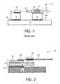
- the laser diode assembly 10has been disclosed by Ziari et al. in U.S. Pat. No. 6,758,610 assigned to JDS Uniphase Corporation and incorporated herein by reference.
- the laser diode assembly 10includes a base 11 , a laser chip submount 12 , a laser chip 13 , a fiber sub-mount 14 including a top section 14 A, and an optical fiber 15 .
- the submounts 12 and 14are affixed to the base 11 with solder layers 16
- the laser chip 13is affixed to the laser chip submount 12 with the solder layer 16 .
- a solder bead 17is used to connect the optical fiber 15 to the fiber submount 14 .
- the fiber 15is metalized to have a metallization layer 18 for improving wettability of the optical fiber 15 by the metal solder material of the bead 17 .
- the top section 14 Ahas low thermal conductivity to serve as a thermal barrier during soldering operation.
- a front surface 19 of the optical fiber 15is lensed to improve fiber coupling efficiency.
- the fiber coupling efficiency of the laser diode assembly 10can vary with ambient temperature even in cases when the laser diode assembly 10 is temperature stabilized using a thermoelectric cooler (TEC).
- the TECis not shown in FIG. 1 .
- the base 11is attached to a top surface of the TEC, and a bottom surface of the TEC is connected to an external heat sink, not shown.
- the ambient temperatureis different from the temperature of the base 11 of the laser diode assembly 10
- the inside and the outside surfaces of the TECare at different temperatures. The temperature difference results in deformation of the inside TEC surface on which the base 11 is mounted, which causes the base 11 of the laser diode assembly 10 to deform.
- the deformation of the base 11results in misalignment of the optical fiber 15 relative to the laser diode chip 13 , which results in a loss of optical fiber coupling efficiency, ultimately leading to a reduction of output optical power and the conversion efficiency of the laser diode assembly 10 .
- Miyokawa et al.disclose a semiconductor laser diode module constructed so as to reduce the temperature dependence of the fiber coupling efficiency.
- the material of a base for supporting a laser chipis selected to match that of a fiber holder.
- the fiber holderhas two parts, one of which is mounted to the base and the other supports the fiber ferrule.
- the part that is mounted to the baseis shaped so that it does not interfere with the laser diode mounting region of the base.
- the module of Miyokawa et al.is rather complex, requiring many laser welding spots to affix all the parts of all the holder elements.
- the inventorsdiscovered that loss of the alignment between the optical fiber and the laser chip was primarily caused by deformation of a platform supporting the laser diode subassembly.
- the inventorsfurther discovered that providing a heat conducting spacer beneath the platform, having an area smaller than the area of the platform, significantly reduces deformation of the platform while providing sufficient heat sinking to keep the laser chip at the required temperature.
- an assemblycomprising:
- a plane of the active layeris perpendicular to the fiber mounting plane, for reduction of sensitivity of the optical coupling between the semiconductor chip and the optical fiber to a variation of temperature of the assembly.
- the semiconductor device subassemblyfurther includes a submount including a bottom surface with a submount mounting area mounted on the platform, for supporting the semiconductor chip and for thermally coupling the semiconductor chip to the platform.
- the fiber mountis preferably attached directly to the submount, to lessen sensitivity of the optical coupling between the semiconductor chip and the optical fiber to deformation of the base.
- a method of assembly of a semiconductor deviceincluding:
- FIG. 1is a side view of a prior-art fiber-coupled laser diode assembly
- FIG. 2is a side cross-sectional view of a semiconductor device assembly according to the present invention.
- FIG. 3is a three-dimensional view of the semiconductor device assembly of FIG. 2 mounted on a thermoelectric cooler (TEC), showing, in exaggerated form, deformation of the TEC;
- TECthermoelectric cooler
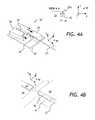
- FIGS. 4A and 4Bare isometric views of the laser diode assembly of FIG. 2 showing attachment of a lensed optical fiber to a vertical surface;
- FIG. 5is an isometric rendering of a packaged laser diode assembly of the invention.
- FIG. 6a side cross-sectional view of a semiconductor device assembly of the invention, having fiber mount attached to the laser diode chip submount;
- FIG. 7is a side cross-sectional view of the semiconductor device assembly of FIG. 6 mounted on a TEC and hermetically packaged.
- a semiconductor device assembly 20 of the present inventionincludes a base 21 , a spacer 22 mounted on the base 21 , a semiconductor device subassembly 23 mounted on the spacer 22 , a fiber mount 26 attached to the semiconductor device subassembly 23 , and an optical fiber 27 attached to the fiber mount 26 .
- the semiconductor device subassembly 23includes a platform 24 , a submount 28 mounted on the platform 24 , and a semiconductor chip 25 mounted on the submount 28 .
- the semiconductor chip 25is thermally coupled to the platform 24 through the submount 28 .
- the semiconductor chip 25is optically coupled to the optical fiber 27 to receive light from an active layer, not shown, of the semiconductor chip 25 .
- the submount 28is optional.
- the semiconductor chip 25is mounted directly on the platform 24 .
- the bottom surface of the platform 24includes a mounting area in contact with the spacer 22 .
- the mounting area of the platform 24is smaller than a total area of the bottom surface of the platform 24 , such that a deformation of the base 21 does not impart, or at least reduces, a deformation of the platform 24 .
- sensitivity of the optical coupling between the semiconductor chip 25 and the optical fiber 27 to a deformation of the base 21is lessened. Since the deformation of the base 21 is caused by a change of ambient temperature, as explained above, the sensitivity of the optical coupling to such ambient temperature changes is also lessened.
- the semiconductor chip 25is preferably a laser diode chip, but it can be any other type of a semiconductor chip that emits light, for example a light-emitting diode (LED) chip.
- the fiber 27is preferably a lensed optical fiber having an anamorphic fiber lens at its tip for improving optical coupling between the semiconductor chip 25 and the fiber 27 .
- the anamorphic lenscan include a biconic or a chisel lens having a focusing power in two planes or only in one plane, a cylindrical lens, and the like.
- a non-anamorphic fiber lenssuch as a conical lens formed at the fiber tip, can be used.
- a separate lenscan also be used.
- the fiber 27can be butt-coupled to the semiconductor chip 25 .
- a plane of the active layer of the semiconductor chip 25is perpendicular to the mounting plane of the optical fiber 27 .
- the plane of the active layeris horizontal
- the fiber mounting planeis vertical, that is, parallel to the plane of FIG. 2 .
- the vertical mounting of the optical fiber 27reduces thermal dependence of the optical coupling between the horizontally mounted semiconductor chip 25 and the optical fiber 27 .
- a length of the mounting area of the submount 28 on the platform 24is between 30% and 80% of a length of the mounting area of the platform 24 on the spacer 22 . These lengths are measured in a direction of a length of the optical fiber 27 . It is also desirable that the submount mounting area be disposed directly over the platform mounting area, as shown in FIG. 2 . Both of these structural features result in lessening of mechanical stress at the semiconductor chip 25 and improve optical stability.
- the spacer 22is preferably made of a material with high thermal conductivity, such as aluminum nitride or copper.
- the thermal conductivity of the spacer 22can be between 200 W/m*K and 400 W/m*K.
- the base 21can be made of an inexpensive steel, although other materials can also be used.
- a semiconductor device assembly 30is shown in a three-dimensional view.
- the semiconductor device assembly 30is similar to the semiconductor device assembly 20 of FIG. 2 , having the spacer 22 , the platform 24 , the submount 28 , the semiconductor device chip 25 , the fiber mount 26 , and the optical fiber 27 , with the exception that the base 21 is replaced with an upper plate 33 of a thermoelectric cooler (TEC) 31 .
- the TEC 31is mounted on an external heat sink 32 .
- the TECis required to maintain the semiconductor device chip 25 at a working temperature, and the external heat sink is required to remove the heat released by TEC operation.
- the TEC 31is shown deformed due to the temperature difference created by TEC operation, as explained above. The deformation of the TEC 31 is exaggerated to illustrate the advantage of using the spacer 22 .
- the semiconductor chip 25is disposed in the XZ plane, as an XYZ coordinate system 40 indicates.
- the optical fiber 27is attached to a vertical surface 41 of the fiber mount 26 , disposed in the YZ plane.
- the plane of the semiconductor device 25is perpendicular to the plane of the vertical surface 41 , which the optical fiber 27 is mounted to.
- the optical fiber 27is attached, preferably using a ultraviolet-curable (UV) epoxy 42 , to the vertical surface 41 .
- UVultraviolet-curable
- the fiber 27bends somewhat in the XZ plane due to thermal mismatches between the fiber 27 , the fiber mount 26 , and the epoxy 42 .
- temperature changesthe degree of bending changes, which results in movement of a tip of the fiber 27 along the X axis. If the fiber 27 were attached to a horizontal surface (parallel to the XZ plane), as is common in the prior art and as is in fact shown on the prior-art FIG. 1 , then the fiber tip would be moving along the Y axis.
- the optical fiber 27is a lensed optical fiber having an anamorphic fiber lens 27 A at its tip for improving the coupling efficiency.
- the fiber lens 27 Ais anamorphic because, as noted above, the semiconductor chip 25 has an anamorphic light field, which needs to be coupled into the round optical fiber 27 .
- the anamorphic fiber lens 27 Ahas mutually orthogonal first and second optical planes parallel to the XZ and YZ planes. The strength of focusing by the anamorphic fiber lens 27 A in the first plane is generally different from the degree of focusing in the second plane.
- a packaged laser diode assembly 50has all the elements of the semiconductor device assembly 20 of FIGS. 2 , 4 A, and 4 B, including the base 21 , the spacer 22 mounted on the base 21 , the platform 24 mounted on the spacer 22 , the submount 28 mounted on the platform 24 , the semiconductor device chip 25 mounted on the submount 28 , the fiber mount 26 mounted on the platform 24 , and the optical fiber 27 mounted to the vertical surface 41 of the submount 26 .
- the laser diode assembly 50also includes a frame 51 (only partially seen in FIG.
- the base 21is attached to a bottom of the frame 51 .
- the base 21is a part of the frame 51 .
- a semiconductor device assembly 60has the same elements as the semiconductor device assembly 20 of FIGS. 2 , 4 A, and 4 B.
- the fiber mount 26is attached to the laser diode chip submount 28 and not to the platform 24 . This additionally improves stability of the optical coupling with respect to deformation of the base 21 , because the deformation of the platform 24 has practically no impact on the position of the fiber mount 26 .
- the optical fiber 27is mounted to the side 41 of the fiber mount 26 . Further, preferably, the optical fiber is lensed, having the anamorphic lens 27 A at its tip.
- a packaged semiconductor device assembly 70 of the inventionhas the same elements as the semiconductor device assembly 60 of FIG. 6 , except for the base 21 , which is replaced with a TEC 72 having an upper plate 73 , a plurality of Peltier elements 74 , and a bottom plate 75 .
- the TEC 72is mounted within a hermetic package 71 having a feedthrough 76 for the optical fiber 27 and electrical feedthroughs 77 for the electrical contacts.
- the fiber mount 26is connected to the submount 28 .
- the optical fiber 27is attached to the fiber mount 26 preferably using a UV curable epoxy. Using UV epoxy is advantageous because it allows one to quickly attach elements together without heating.
- UV epoxiescompared to other types of epoxies
- the hermetically sealed package 71is used.
- other types of epoxiescan be used, as well as glass or metal soldering, brazing, or laser welding.
- a non-hermetic packageis also usable, although a hermetic package is generally preferable.
- the semiconductor device assemblies 20 , 30 , 50 , 60 , and 70can be manufactured following the general steps of:
- step (c)the subassembly is aligned on the platform 24 , which is subsequently attached to the spacer 22 .
- the subassemblycan be aligned already mounted on the TEC 31 or 72 , as well.
- the step (c)can include a sub-step (c1) of aligning the optical fiber 27 to the semiconductor chip 25 for receiving light therefrom, and a sub-step (c2) of attaching the optical fiber 25 to the fiber mount 26 such that a plane of the active layer (XZ plane) is perpendicular to the fiber mounting plane (YZ plane).
- the step (c)includes mounting the submount 28 on the platform 24 and mounting the semiconductor chip 25 to the submount 28 , not necessarily in the exact order stated.
- the step (c)also includes mounting the fiber mount 26 to the submount 28 .
Landscapes
- Physics & Mathematics (AREA)
- General Physics & Mathematics (AREA)
- Optics & Photonics (AREA)
- Optical Couplings Of Light Guides (AREA)
Abstract
Description
- a base;
- a spacer mounted on the base;
- a semiconductor device subassembly including a platform having a bottom surface with a platform mounting area mounted on the spacer, and a semiconductor chip having an active layer, the semiconductor chip thermally coupled to the platform for removing heat from the semiconductor chip;
- a fiber mount attached to the semiconductor device subassembly, the fiber mount having a fiber mounting plane; and
- an optical fiber attached to the fiber mount in the fiber mounting plane and optically coupled to the semiconductor chip for receiving light therefrom;
- wherein the platform mounting area is smaller than a total area of the bottom surface of the platform, whereby sensitivity of the optical coupling between the semiconductor chip and the optical fiber to deformation of the base is lessened.
- (a) providing a base;
- (b) mounting a spacer on the base;
- (c) providing a semiconductor device subassembly including: a platform having a bottom surface with a platform mounting area; a semiconductor chip having an active layer, the semiconductor chip thermally coupled to the platform for removing heat from the semiconductor chip; a fiber mount attached to the semiconductor device subassembly, the fiber mount having a fiber mounting plane; and an optical fiber attached to the fiber mount in the fiber mounting plane and optically coupled to the semiconductor chip for receiving light therefrom; and
- (d) mounting the platform mounting area on the spacer so that the platform mounting area is smaller than a total area of the bottom surface of the platform, whereby sensitivity of the optical coupling between the semiconductor chip and the optical fiber to deformation of the base is lessened.
- providing the
base 21 and/or theTEC subassembly 23 will be mounted; - providing the
spacer 22 and mounting thespacer 22 on thebase 21 and/or TEC; - providing the subassembly including the
semiconductor chip 25 mounted on thesubmount 28 mounted on theplatform 24, and anoptical fiber 27 aligned for optical coupling to thesemiconductor chip 25 and mounted on thefiber mount 26 attached to theplatform 24 or directly to thesubmount 28, as the case may be; - mounting the
platform 24 on thespacer 22 so that the platform mounting area is smaller than a total area of the bottom surface of theplatform 24. As noted above, this way of mounting helps reducing sensitivity of the optical coupling between thesemiconductor chip 25 and theoptical fiber 27 to deformation of thebase 21.
- providing the
Claims (17)
Priority Applications (1)
| Application Number | Priority Date | Filing Date | Title |
|---|---|---|---|
| US12/843,823US8475056B2 (en) | 2009-07-28 | 2010-07-26 | Semiconductor device assembly |
Applications Claiming Priority (2)
| Application Number | Priority Date | Filing Date | Title |
|---|---|---|---|
| US22917109P | 2009-07-28 | 2009-07-28 | |
| US12/843,823US8475056B2 (en) | 2009-07-28 | 2010-07-26 | Semiconductor device assembly |
Publications (2)
| Publication Number | Publication Date |
|---|---|
| US20110026877A1 US20110026877A1 (en) | 2011-02-03 |
| US8475056B2true US8475056B2 (en) | 2013-07-02 |
Family
ID=43526951
Family Applications (2)
| Application Number | Title | Priority Date | Filing Date |
|---|---|---|---|
| US12/843,823Active2031-08-16US8475056B2 (en) | 2009-07-28 | 2010-07-26 | Semiconductor device assembly |
| US12/844,698Active2031-06-29US9036678B2 (en) | 2009-07-28 | 2010-07-27 | Light emitting semiconductor device |
Family Applications After (1)
| Application Number | Title | Priority Date | Filing Date |
|---|---|---|---|
| US12/844,698Active2031-06-29US9036678B2 (en) | 2009-07-28 | 2010-07-27 | Light emitting semiconductor device |
Country Status (2)
| Country | Link |
|---|---|
| US (2) | US8475056B2 (en) |
| CN (2) | CN101986178B (en) |
Cited By (4)
| Publication number | Priority date | Publication date | Assignee | Title |
|---|---|---|---|---|
| US20140097232A1 (en)* | 2011-06-16 | 2014-04-10 | Fujikura Ltd. | Bonding method and production method |
| US9728935B2 (en) | 2015-06-05 | 2017-08-08 | Lumentum Operations Llc | Chip-scale package and semiconductor device assembly |
| US10566761B2 (en) | 2015-07-16 | 2020-02-18 | Furukawa Electric Co., Ltd. | Semiconductor laser module |
| US20230280551A1 (en)* | 2020-11-19 | 2023-09-07 | Mitsubishi Electric Corporation | Optical module |
Families Citing this family (19)
| Publication number | Priority date | Publication date | Assignee | Title |
|---|---|---|---|---|
| JP2009267386A (en)* | 2008-03-31 | 2009-11-12 | Furukawa Electric Co Ltd:The | Semiconductor laser module and suppression member |
| US8475056B2 (en)* | 2009-07-28 | 2013-07-02 | Jds Uniphase Corporation | Semiconductor device assembly |
| WO2012148682A1 (en)* | 2011-04-29 | 2012-11-01 | Bae Systems Information And Electronic Systems Integration Inc. | Temperature control of a fiber laser system |
| JP2013004752A (en)* | 2011-06-16 | 2013-01-07 | Fujikura Ltd | Laser module |
| CN102412500A (en)* | 2011-11-30 | 2012-04-11 | 江苏飞格光电有限公司 | Packaging method of semiconductor laser |
| JP6123977B2 (en)* | 2012-02-07 | 2017-05-10 | セイコーエプソン株式会社 | Atomic oscillator |
| US20130215924A1 (en)* | 2012-02-16 | 2013-08-22 | John McKenna Brennan | Non-hermetic, multi-emitter laser pump packages and methods for forming the same |
| CN103018859A (en)* | 2013-01-08 | 2013-04-03 | 中国电子科技集团公司第四十四研究所 | Precise positioning and fixing structure for optical fiber coupling end |
| JP5834125B1 (en) | 2014-09-29 | 2015-12-16 | 株式会社フジクラ | Optical fiber module |
| WO2016093262A1 (en)* | 2014-12-11 | 2016-06-16 | 株式会社フジクラ | Optical module |
| CN105572817B (en)* | 2015-12-24 | 2017-12-22 | 西安电子科技大学 | It is a kind of to be used for integrated special-shaped end face fiber coupler |
| JP6667307B2 (en)* | 2016-02-04 | 2020-03-18 | 古河電気工業株式会社 | Optical coupling structure between optical fiber and semiconductor laser |
| US10056732B2 (en)* | 2016-07-20 | 2018-08-21 | Coherent, Inc. | Mechanically isolated optically pumped semiconductor laser |
| WO2019155602A1 (en)* | 2018-02-09 | 2019-08-15 | 三菱電機株式会社 | Optical module |
| JP2018186289A (en)* | 2018-07-05 | 2018-11-22 | セイコーエプソン株式会社 | Light emitting device module and atomic oscillator |
| WO2021120433A1 (en) | 2019-12-20 | 2021-06-24 | 青岛海信宽带多媒体技术有限公司 | Optical module |
| CN113009646B (en)* | 2019-12-20 | 2022-07-29 | 青岛海信宽带多媒体技术有限公司 | Optical module |
| JP2022180123A (en)* | 2021-05-24 | 2022-12-06 | 日亜化学工業株式会社 | Light-emitting device and method for manufacturing light-emitting device |
| CN113376767B (en)* | 2021-05-28 | 2022-08-26 | 上海曦智科技有限公司 | Chip packaging structure and optical computing device |
Citations (14)
| Publication number | Priority date | Publication date | Assignee | Title |
|---|---|---|---|---|
| US4722586A (en) | 1985-04-12 | 1988-02-02 | Tektronix, Inc. | Electro-optical transducer module |
| US5682453A (en) | 1994-04-18 | 1997-10-28 | Gould Electronics Inc. | Method of securing optical fiber components, devices and fibers to the same or to mounting fixtures |
| US5692086A (en) | 1995-10-25 | 1997-11-25 | The Boeing Company | Optical fiber locking submount and hermetic feedthrough assembly |
| US5926599A (en) | 1996-06-13 | 1999-07-20 | Corning Incorporated | Optical device and fusion seal |
| US6075914A (en) | 1997-11-21 | 2000-06-13 | Bookham Technology Limited | Apparatus for connecting an optical fiber to an optical device |
| US6574411B2 (en) | 2000-02-07 | 2003-06-03 | Itf Optical Technologies Inc. | Bonding optical fibers to substrates |
| US20040033034A1 (en)* | 2000-05-31 | 2004-02-19 | The Furukawa Electric Co., Ltd. | Semiconductor laser diode module |
| US6758610B2 (en) | 2001-12-10 | 2004-07-06 | Jds Uniphase Corporation | Optical component attachment to optoelectronic packages |
| US6883978B2 (en) | 2003-06-26 | 2005-04-26 | Matsushita Electric Industrial Co., Ltd. | Low cost package design for fiber coupled optical component |
| US6961357B2 (en) | 2003-05-20 | 2005-11-01 | Opnext Japan, Inc. | Semiconductor laser module |
| US7062133B2 (en) | 2003-04-24 | 2006-06-13 | Ahura Corporation | Methods and apparatus for alignment and assembly of optoelectronic components |
| US7263266B2 (en) | 2002-12-10 | 2007-08-28 | Picometrix, Llc | Precision fiber attachment |
| US7293922B2 (en) | 2004-06-02 | 2007-11-13 | Matsushita Electric Industrial Co., Ltd. | Non-mechanical adjustment of an optical fiber to an optical output port |
| US20110026558A1 (en)* | 2009-07-28 | 2011-02-03 | Jds Uniphase Corporation | light emitting semiconductor device |
Family Cites Families (23)
| Publication number | Priority date | Publication date | Assignee | Title |
|---|---|---|---|---|
| US3840889A (en)* | 1973-07-11 | 1974-10-08 | Rca Corp | Laser diode package formed of ceramic and metal materials having high electrical and thermal conductivity |
| JPS57138191A (en)* | 1981-02-19 | 1982-08-26 | Kokusai Denshin Denwa Co Ltd <Kdd> | United structure of semiconductor laser and optical fiber |
| US4752109A (en)* | 1986-09-02 | 1988-06-21 | Amp Incorporated | Optoelectronics package for a semiconductor laser |
| FR2605418B1 (en)* | 1986-10-17 | 1990-04-20 | Thomson Semiconducteurs | MODULE FOR COUPLING BETWEEN A SEMICONDUCTOR DEVICE AND AN OPTICAL FIBER, AND METHOD FOR ALIGNING THE SEMICONDUCTOR DEVICE AND THE FIBER |
| US4871226A (en)* | 1987-10-01 | 1989-10-03 | United Technologies Corporation | Mounting of optical fibers to integrated optical chips |
| FR2623297B1 (en)* | 1987-11-13 | 1991-09-27 | Cit Alcatel | COUPLING DEVICE BETWEEN AN OPTICAL FIBER AND AN OPTOELECTRONIC COMPONENT |
| US5163113A (en)* | 1990-07-19 | 1992-11-10 | Gte Laboratories Incorporated | Laser-to-fiber coupling apparatus |
| US5619609A (en)* | 1996-02-02 | 1997-04-08 | E-Tek Dynamics, Inc. | Fiberoptic support clip |
| US6130444A (en)* | 1998-02-27 | 2000-10-10 | Nec Corporation | Optical fiber secured with a photosetting resin covered with a UV light-transmissive plate |
| JP3345853B2 (en)* | 1998-11-13 | 2002-11-18 | 古河電気工業株式会社 | Laser diode module and manufacturing method thereof |
| US6516130B1 (en)* | 1998-12-30 | 2003-02-04 | Newport Corporation | Clip that aligns a fiber optic cable with a laser diode within a fiber optic module |
| KR100322134B1 (en)* | 1999-02-06 | 2002-03-18 | 윤종용 | Apparatus for aligning optical source with optical fiber and optical source module comprising it |
| KR20010025777A (en)* | 1999-09-01 | 2001-04-06 | 이형도 | Method of processing multi-key in key inputting device |
| JP4167378B2 (en)* | 2000-03-28 | 2008-10-15 | 京セラ株式会社 | Optical element module |
| JP3518491B2 (en)* | 2000-06-26 | 2004-04-12 | 株式会社日立製作所 | Optical coupling device |
| US6659659B1 (en)* | 2001-04-11 | 2003-12-09 | Optical Communication Products, Inc. | High-speed optical sub-assembly utilizing ceramic substrate, direct coupling and laser welding |
| US6792012B2 (en)* | 2001-04-30 | 2004-09-14 | Jds Uniphase Corporation | Laser pump module with reduced tracking error |
| US7044653B2 (en)* | 2001-09-07 | 2006-05-16 | Coherent, Inc. | Microassembly and method for using same |
| US7158549B2 (en)* | 2003-12-01 | 2007-01-02 | Bookham Technology Plc | Support structure for an optical device |
| US6905354B1 (en)* | 2003-12-10 | 2005-06-14 | Intel Corporation | U-clip for optical device alignment |
| WO2006025876A2 (en)* | 2004-08-30 | 2006-03-09 | Ahura Corporation | External cavity wavelength stabilized raman lasers insensitive to temperature and/or external mechanical stresses, and raman analyzer utilizing the same |
| JP4335778B2 (en)* | 2004-10-25 | 2009-09-30 | スタンレー電気株式会社 | Optical fiber connection structure |
| US7869475B2 (en)* | 2006-07-12 | 2011-01-11 | Pgt Photonics S.P.A. | Misalignment prevention in an external cavity laser having temperature stabilisation of the resonator and the gain medium |
- 2010
- 2010-07-26USUS12/843,823patent/US8475056B2/enactiveActive
- 2010-07-27CNCN201010237756.XApatent/CN101986178B/enactiveActive
- 2010-07-27USUS12/844,698patent/US9036678B2/enactiveActive
- 2010-07-28CNCN201010238868.7Apatent/CN101986179B/enactiveActive
Patent Citations (17)
| Publication number | Priority date | Publication date | Assignee | Title |
|---|---|---|---|---|
| US4722586A (en) | 1985-04-12 | 1988-02-02 | Tektronix, Inc. | Electro-optical transducer module |
| US5682453A (en) | 1994-04-18 | 1997-10-28 | Gould Electronics Inc. | Method of securing optical fiber components, devices and fibers to the same or to mounting fixtures |
| US5692086A (en) | 1995-10-25 | 1997-11-25 | The Boeing Company | Optical fiber locking submount and hermetic feedthrough assembly |
| US5926599A (en) | 1996-06-13 | 1999-07-20 | Corning Incorporated | Optical device and fusion seal |
| US6075914A (en) | 1997-11-21 | 2000-06-13 | Bookham Technology Limited | Apparatus for connecting an optical fiber to an optical device |
| US6574411B2 (en) | 2000-02-07 | 2003-06-03 | Itf Optical Technologies Inc. | Bonding optical fibers to substrates |
| US7030422B2 (en) | 2000-05-31 | 2006-04-18 | The Furukawa Electric Co., Ltd. | Semiconductor laser diode module |
| US20040033034A1 (en)* | 2000-05-31 | 2004-02-19 | The Furukawa Electric Co., Ltd. | Semiconductor laser diode module |
| US6734517B2 (en) | 2000-05-31 | 2004-05-11 | The Furukawa Electric Co., Ltd. | Semiconductor laser diode module |
| US6758610B2 (en) | 2001-12-10 | 2004-07-06 | Jds Uniphase Corporation | Optical component attachment to optoelectronic packages |
| US7263266B2 (en) | 2002-12-10 | 2007-08-28 | Picometrix, Llc | Precision fiber attachment |
| US7062133B2 (en) | 2003-04-24 | 2006-06-13 | Ahura Corporation | Methods and apparatus for alignment and assembly of optoelectronic components |
| US7409125B2 (en) | 2003-04-24 | 2008-08-05 | Ahura Corporation | Methods and apparatus for alignment and assembly of optoelectronic components |
| US6961357B2 (en) | 2003-05-20 | 2005-11-01 | Opnext Japan, Inc. | Semiconductor laser module |
| US6883978B2 (en) | 2003-06-26 | 2005-04-26 | Matsushita Electric Industrial Co., Ltd. | Low cost package design for fiber coupled optical component |
| US7293922B2 (en) | 2004-06-02 | 2007-11-13 | Matsushita Electric Industrial Co., Ltd. | Non-mechanical adjustment of an optical fiber to an optical output port |
| US20110026558A1 (en)* | 2009-07-28 | 2011-02-03 | Jds Uniphase Corporation | light emitting semiconductor device |
Cited By (5)
| Publication number | Priority date | Publication date | Assignee | Title |
|---|---|---|---|---|
| US20140097232A1 (en)* | 2011-06-16 | 2014-04-10 | Fujikura Ltd. | Bonding method and production method |
| US9728935B2 (en) | 2015-06-05 | 2017-08-08 | Lumentum Operations Llc | Chip-scale package and semiconductor device assembly |
| US10566761B2 (en) | 2015-07-16 | 2020-02-18 | Furukawa Electric Co., Ltd. | Semiconductor laser module |
| US20230280551A1 (en)* | 2020-11-19 | 2023-09-07 | Mitsubishi Electric Corporation | Optical module |
| US12292604B2 (en)* | 2020-11-19 | 2025-05-06 | Mitsubishi Electric Corporation | Optical module |
Also Published As
| Publication number | Publication date |
|---|---|
| CN101986179B (en) | 2015-05-13 |
| US20110026558A1 (en) | 2011-02-03 |
| US20110026877A1 (en) | 2011-02-03 |
| CN101986178B (en) | 2015-05-13 |
| CN101986179A (en) | 2011-03-16 |
| US9036678B2 (en) | 2015-05-19 |
| CN101986178A (en) | 2011-03-16 |
Similar Documents
| Publication | Publication Date | Title |
|---|---|---|
| US8475056B2 (en) | Semiconductor device assembly | |
| US6712528B2 (en) | Optical bench for an opto-electronic device | |
| CN102043208B (en) | Cooled laser module | |
| US6888860B2 (en) | Low cost optical bench having high thermal conductivity | |
| US8644357B2 (en) | High reliability laser emitter modules | |
| JP4290893B2 (en) | Optoelectronic assembly | |
| US6786627B2 (en) | Light generating module | |
| JPH09138329A (en) | Opto-semiconductor array module, assembling method thereof, and external board mounting structure | |
| US20120099816A1 (en) | Photonics module and method of manufacturing | |
| EP2256880B1 (en) | Laser light source module | |
| CN105705975A (en) | Method and system for an optical communication device | |
| US8687663B2 (en) | Laser device | |
| US11223182B2 (en) | Method of manufacturing optical module | |
| WO2014017250A1 (en) | Light emitting device, method for manufacturing same, and package member | |
| US7633992B1 (en) | Laser module including jointly arranged isolator and fiber sleeve | |
| US10680405B2 (en) | Semiconductor light-emitting device | |
| CA2813726A1 (en) | Photonics module and method of manufacturing | |
| US7061025B2 (en) | Optoelectronic device packaging assemblies and methods of making the same | |
| US10050410B2 (en) | Coefficient of thermal expansion (CTE) matched transistor outline (TO) header | |
| EP1271209A1 (en) | Optical bench for an opto-electronic device | |
| JP2004294746A (en) | Optical semiconductor module | |
| JP2004341370A (en) | Optical module | |
| KR970031116A (en) | Laser diode modules for optical amplification and process for preparing them | |
| WO2002054118A2 (en) | Low cost optical bench having high thermal conductivity |
Legal Events
| Date | Code | Title | Description |
|---|---|---|---|
| AS | Assignment | Owner name:JDS UNIPHASE CORPORATION, CALIFORNIA Free format text:ASSIGNMENT OF ASSIGNORS INTEREST;ASSIGNORS:YALAMANCHILI, PRASAD;QIU, XIANGDONG;RAJU, REDDY;AND OTHERS;REEL/FRAME:025096/0228 Effective date:20100826 | |
| STCF | Information on status: patent grant | Free format text:PATENTED CASE | |
| AS | Assignment | Owner name:LUMENTUM OPERATIONS LLC, CALIFORNIA Free format text:ASSIGNMENT OF ASSIGNORS INTEREST;ASSIGNOR:JDS UNIPHASE CORPORATION;REEL/FRAME:036420/0340 Effective date:20150731 | |
| FEPP | Fee payment procedure | Free format text:PAYOR NUMBER ASSIGNED (ORIGINAL EVENT CODE: ASPN); ENTITY STATUS OF PATENT OWNER: LARGE ENTITY Free format text:PAYER NUMBER DE-ASSIGNED (ORIGINAL EVENT CODE: RMPN); ENTITY STATUS OF PATENT OWNER: LARGE ENTITY | |
| AS | Assignment | Owner name:LUMENTUM OPERATIONS LLC, CALIFORNIA Free format text:CORRECTIVE ASSIGNMENT TO CORRECT INCORRECT PATENTS 7,868,247 AND 6,476,312 ON PAGE A-A33 PREVIOUSLY RECORDED ON REEL 036420 FRAME 0340. ASSIGNOR(S) HEREBY CONFIRMS THE ASSIGNMENT;ASSIGNOR:JDS UNIPHASE CORPORATION;REEL/FRAME:037562/0513 Effective date:20150731 Owner name:LUMENTUM OPERATIONS LLC, CALIFORNIA Free format text:CORRECTIVE ASSIGNMENT TO CORRECT THE PATENTS LISTED ON PAGE A-A33 PREVIOUSLY RECORDED ON REEL 036420 FRAME 0340. ASSIGNOR(S) HEREBY CONFIRMS THE PATENT NUMBERS 7,868,247 AND 6,476,312 WERE LISTED IN ERROR AND SHOULD BE REMOVED;ASSIGNOR:JDS UNIPHASE CORPORATION;REEL/FRAME:037562/0513 Effective date:20150731 | |
| AS | Assignment | Owner name:LUMENTUM OPERATIONS LLC, CALIFORNIA Free format text:CORRECTIVE ASSIGNMENT TO CORRECT THE PATENTS LISTED ON PAGE A-A33 PATENT NUMBERS 7,868,247 AND 6,476,312 WERE LISTED IN ERROR AND SHOULD BE REMOVED. PREVIOUSLY RECORDED ON REEL 036420 FRAME 0340. ASSIGNOR(S) HEREBY CONFIRMS THE ASSIGNMENT;ASSIGNOR:JDS UNIPHASE CORPORATION;REEL/FRAME:037627/0641 Effective date:20150731 Owner name:LUMENTUM OPERATIONS LLC, CALIFORNIA Free format text:CORRECTIVE ASSIGNMENT TO CORRECT PATENTS 7,868,247 AND 6,476,312 LISTED ON PAGE A-A33 PREVIOUSLY RECORDED ON REEL 036420 FRAME 0340. ASSIGNOR(S) HEREBY CONFIRMS THE ASSIGNMENT;ASSIGNOR:JDS UNIPHASE CORPORATION;REEL/FRAME:037627/0641 Effective date:20150731 | |
| FPAY | Fee payment | Year of fee payment:4 | |
| AS | Assignment | Owner name:DEUTSCHE BANK AG NEW YORK BRANCH, AS COLLATERAL AGENT, NEW YORK Free format text:PATENT SECURITY AGREEMENT;ASSIGNORS:LUMENTUM OPERATIONS LLC;OCLARO FIBER OPTICS, INC.;OCLARO, INC.;REEL/FRAME:047788/0511 Effective date:20181210 Owner name:DEUTSCHE BANK AG NEW YORK BRANCH, AS COLLATERAL AG Free format text:PATENT SECURITY AGREEMENT;ASSIGNORS:LUMENTUM OPERATIONS LLC;OCLARO FIBER OPTICS, INC.;OCLARO, INC.;REEL/FRAME:047788/0511 Effective date:20181210 | |
| AS | Assignment | Owner name:OCLARO FIBER OPTICS, INC., CALIFORNIA Free format text:RELEASE BY SECURED PARTY;ASSIGNOR:DEUTSCHE AG NEW YORK BRANCH;REEL/FRAME:051287/0556 Effective date:20191212 Owner name:OCLARO, INC., CALIFORNIA Free format text:RELEASE BY SECURED PARTY;ASSIGNOR:DEUTSCHE AG NEW YORK BRANCH;REEL/FRAME:051287/0556 Effective date:20191212 Owner name:LUMENTUM OPERATIONS LLC, CALIFORNIA Free format text:RELEASE BY SECURED PARTY;ASSIGNOR:DEUTSCHE AG NEW YORK BRANCH;REEL/FRAME:051287/0556 Effective date:20191212 | |
| MAFP | Maintenance fee payment | Free format text:PAYMENT OF MAINTENANCE FEE, 8TH YEAR, LARGE ENTITY (ORIGINAL EVENT CODE: M1552); ENTITY STATUS OF PATENT OWNER: LARGE ENTITY Year of fee payment:8 | |
| MAFP | Maintenance fee payment | Free format text:PAYMENT OF MAINTENANCE FEE, 12TH YEAR, LARGE ENTITY (ORIGINAL EVENT CODE: M1553); ENTITY STATUS OF PATENT OWNER: LARGE ENTITY Year of fee payment:12 |