US8472146B2 - Current perpendicular magnetoresistive sensor with a dummy shield for capacitance balancing - Google Patents
Current perpendicular magnetoresistive sensor with a dummy shield for capacitance balancingDownload PDFInfo
- Publication number
- US8472146B2 US8472146B2US12/870,561US87056110AUS8472146B2US 8472146 B2US8472146 B2US 8472146B2US 87056110 AUS87056110 AUS 87056110AUS 8472146 B2US8472146 B2US 8472146B2
- Authority
- US
- United States
- Prior art keywords
- magnetic
- shield
- electrically conductive
- substrate
- dummy
- Prior art date
- Legal status (The legal status is an assumption and is not a legal conclusion. Google has not performed a legal analysis and makes no representation as to the accuracy of the status listed.)
- Expired - Fee Related, expires
Links
Images


Classifications
- G—PHYSICS
- G11—INFORMATION STORAGE
- G11B—INFORMATION STORAGE BASED ON RELATIVE MOVEMENT BETWEEN RECORD CARRIER AND TRANSDUCER
- G11B5/00—Recording by magnetisation or demagnetisation of a record carrier; Reproducing by magnetic means; Record carriers therefor
- G11B5/127—Structure or manufacture of heads, e.g. inductive
- G11B5/33—Structure or manufacture of flux-sensitive heads, i.e. for reproduction only; Combination of such heads with means for recording or erasing only
- G11B5/39—Structure or manufacture of flux-sensitive heads, i.e. for reproduction only; Combination of such heads with means for recording or erasing only using magneto-resistive devices or effects
- G11B5/3903—Structure or manufacture of flux-sensitive heads, i.e. for reproduction only; Combination of such heads with means for recording or erasing only using magneto-resistive devices or effects using magnetic thin film layers or their effects, the films being part of integrated structures
- G11B5/398—Specially shaped layers
- G—PHYSICS
- G11—INFORMATION STORAGE
- G11B—INFORMATION STORAGE BASED ON RELATIVE MOVEMENT BETWEEN RECORD CARRIER AND TRANSDUCER
- G11B5/00—Recording by magnetisation or demagnetisation of a record carrier; Reproducing by magnetic means; Record carriers therefor
- G11B5/127—Structure or manufacture of heads, e.g. inductive
- G11B5/33—Structure or manufacture of flux-sensitive heads, i.e. for reproduction only; Combination of such heads with means for recording or erasing only
- G11B5/39—Structure or manufacture of flux-sensitive heads, i.e. for reproduction only; Combination of such heads with means for recording or erasing only using magneto-resistive devices or effects
- G11B5/3903—Structure or manufacture of flux-sensitive heads, i.e. for reproduction only; Combination of such heads with means for recording or erasing only using magneto-resistive devices or effects using magnetic thin film layers or their effects, the films being part of integrated structures
- G11B5/3906—Details related to the use of magnetic thin film layers or to their effects
- G11B5/3912—Arrangements in which the active read-out elements are transducing in association with active magnetic shields, e.g. magnetically coupled shields
- H—ELECTRICITY
- H05—ELECTRIC TECHNIQUES NOT OTHERWISE PROVIDED FOR
- H05K—PRINTED CIRCUITS; CASINGS OR CONSTRUCTIONAL DETAILS OF ELECTRIC APPARATUS; MANUFACTURE OF ASSEMBLAGES OF ELECTRICAL COMPONENTS
- H05K3/00—Apparatus or processes for manufacturing printed circuits
Definitions
- the present inventionrelates to magnetic heads for data recording, and more particularly to a magnetic head that includes a current perpendicular to plane magnetoresistive sensor that has capacitance balancing for improved performance.
- the heart of a computer's long term memoryis an assembly that is referred to as a magnetic hard disk drive.
- the magnetic hard disk driveincludes a rotating magnetic disk, write and read heads that are suspended by a suspension arm adjacent to a surface of the rotating magnetic disk and an actuator that swings the suspension arm to place the read and write heads over selected circular tracks on the rotating disk.
- the read and write headsare directly located on a slider that has an air bearing surface (ABS).
- ABSair bearing surface
- the suspension armbiases the slider toward the surface of the disk, and when the disk rotates, air adjacent to the disk moves along with the surface of the disk.
- the sliderflies over the surface of the disk on a cushion of this moving air.
- the write and read headsare employed for writing magnetic transitions to and reading magnetic transitions from the rotating disk.
- the read and write headsare connected to processing circuitry that operates according to a computer program to implement the writing and reading functions.
- magnetic tape drivesare employed to store magnetic data, such as for long term storage.
- Such tape drive devicesinclude a slider that includes a magnetoresistive sensor and a magnetic write head. A magnetic tape slides over the surface allowing data to be written to or read from the tape.
- the write headcan include a coil that passes through a magnetic yoke that includes a write pole and a return pole. Current conducted to the coil layer induces a magnetic flux in the pole pieces which causes a write field to emit from the write pole for the purpose of writing a magnetic transition in tracks on the moving media, such as in circular tracks on the rotating disk.
- a sensorsuch as a GMR or TMR sensor has been employed for sensing magnetic fields from the rotating magnetic disk.
- Such sensorsuse a spin valve magnetic design, including a nonmagnetic conductive spacer layer, or nonmagnetic insulating barrier layer, sandwiched between first and second ferromagnetic layers, referred to as a pinned or reference layer and a free layer.
- First and second leadsare connected to the sensor for conducting a sense current there-through.
- the magnetization of the pinned layeris pinned perpendicular to the air bearing surface (ABS) and the magnetic moment of the free layer is located parallel to the ABS, but free to rotate in response to external magnetic fields.
- the magnetization of the pinned layeris typically pinned by exchange coupling with an antiferromagnetic layer.
- the present inventionprovides a magnetic head that includes a substrate, and a magnetoresistive sensor sandwiched between first and second electrically conductive magnetic leads.
- a non-magnetic, electrically insulating layerseparates the first magnetic shield from the substrate, and a dummy shield is formed on the non-magnetic, electrically insulating layer, the dummy shield being electrically connected with the second, electrically conductive magnetic shield.
- the dummy magnetic shieldadvantageously balances the capacitive coupling between the first magnetic shield and the substrate.
- the dummy magnetic shieldis formed so that it has the same capacitive coupling with the substrate as the first magnetic shield does. Because the dummy shield is electrically connected with the second magnetic shield the capacitive load across the read head is completely balanced.
- the dummy magnetic shieldcan be formed in the same process steps used to form the first magnetic shield.
- the balanced capacitive couplingtherefore, adds no additional manufacturing cost or complexity.
- FIG. 1is a schematic illustration of a disk drive system in which the invention might be embodied
- FIG. 2is an ABS view of a slider, taken from line 2 - 2 of FIG. 1 , illustrating the location of a magnetic head thereon;
- FIG. 3is a schematic ABS view of a sensor according to an embodiment of the invention.
- FIG. 4is an enlarged schematic ABS view of a prior art magnetic head exhibiting unbalanced capacitive coupling between the sensor and the substrate;
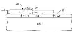
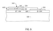
- FIG. 5is an enlarged schematic ABS view of a magnetic head according to an embodiment of the invention, illustrating a structure for balanced capacitance
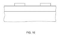
- FIGS. 6-10are cross sectional views showing a magnetic read head in various intermediate stages of manufacture, illustrating a method of manufacturing a read head with a dummy shield for capacitive balance.
- FIG. 1there is shown a disk drive 100 embodying this invention.
- at least one rotatable magnetic disk 112is supported on a spindle 114 and rotated by a disk drive motor 118 .
- the magnetic recording on each diskis in the form of annular patterns of concentric data tracks (not shown) on the magnetic disk 112 .
- At least one slider 113is positioned near the magnetic disk 112 , each slider 113 supporting one or more magnetic head assemblies 121 . As the magnetic disk rotates, slider 113 moves radially in and out over the disk surface 122 so that the magnetic head assembly 121 may access different tracks of the magnetic disk where desired data are written.
- Each slider 113is attached to an actuator arm 119 by way of a suspension 115 .
- the suspension 115provides a slight spring force which biases slider 113 against the disk surface 122 .
- Each actuator arm 119is attached to an actuator means 127 .
- the actuator means 127 as shown in FIG. 1may be a voice coil motor (VCM).
- the VCMcomprises a coil movable within a fixed magnetic field, the direction and speed of the coil movements being controlled by the motor current signals supplied by controller 129 .
- the rotation of the magnetic disk 112generates an air bearing between the slider 113 and the disk surface 122 which exerts a force on the slider.
- the air bearingthus counter-balances the slight spring force of suspension 115 and supports the slider 113 off and slightly above the disk surface by a small, substantially constant spacing during normal operation.
- control unit 129The various components of the disk storage system are controlled in operation by control signals generated by control unit 129 , such as access control signals and internal clock signals.
- control unit 129comprises logic control circuits, storage means and a microprocessor.
- the control unit 129generates control signals to control various system operations such as drive motor control signals on line 123 and head position and seek control signals on line 128 .
- the control signals on line 128provide the desired current profiles to optimally move and position slider 113 to the desired data track on disk 112 .
- Write and read signalsare communicated to and from write and read heads 121 by way of recording channel 125 .
- FIG. 2is an ABS view of the slider 113 , and as can be seen the magnetic head including an inductive write head and a read sensor, is located at a trailing edge of the slider.
- the magnetic head including an inductive write head and a read sensoris located at a trailing edge of the slider.
- FIG. 3shows an example of a current perpendicular to plane magnetoresistive sensor 300 , such as might be used in a magnetic disk drive or a magnetic tape drive.
- the sensor 300is sandwiched between first and second electrically conductive, magnetic shields 302 , 304 that also function as electrical leads for conducting a sense current through the sensor in a direction perpendicular to the planes of the layers of the sensor 300 .
- the sensor 300includes a magnetic pinned layer structure 306 , a magnetic free layer structure 308 and a non-magnetic layer 310 sandwiched between the pinned layer structure 306 and the free layer structure 308 .
- the non-magnetic layer 310is an electrically conductive spacer layer such as Cu.
- the sensor 300is a tunnel junction magnetoresistive (TMR) sensor, then the non-magnetic layer 310 is a thin electrically insulating barrier layer.
- the pinned layer structurecan be an antiparallel coupled (AP coupled) structure including a first magnetic layer (AP 1 ) 312 , a second magnetic layer (AP 2 ) 314 and a non-magnetic antiparallel coupling layer 316 such as Ru sandwiched between the AP 1 and AP 2 layers 312 , 314 .
- the AP 1 layer 312can be exchange coupled with a layer of antiferromagnetic material (AFM layer) 318 , which strongly pins the magnetization of the AP 1 layer 312 in a desired direction perpendicular to the ABS.
- AFM layerantiferromagnetic material
- Antiparallel coupling between the AP 1 and AP 2 layerspins the magnetization of the AP 2 layer in a second direction that is antiparallel with the AP 1 layer 312 and perpendicular with the ABS.
- the free layerhas a magnetization that is biased in a direction parallel with the ABS by magnetostatic coupling with first and second hard magnetic bias layers 320 , 322 .
- the hard bias layers 320 , 322are separated from the sensor layers 300 and from at least one of the shield/lead layers 302 by an electrically insulating layer 324 such as alumina.
- a capping layer 330can be provided at the top of the sensor stack 300 to protect the free layer 308 during manufacture.
- the sensor 300 , shields 302 , 304 , bias layers 320 , 322 and insulation layers 324form a magnetic head 325 that is formed on a non-magnetic, electrically insulating layer 326 .
- the electrically insulating layer 326separates the head 325 from a substrate material 328 .
- the substrate 328is formed of a hard, electrically conductive material such a composite material of alumina (Al 2 O 3 ) and titanium carbide (TC), which is generally abbreviated as AlTiC.
- the electrically insulating layer 326can be constructed of a material such as alumina Al 2 O 3 .
- FIG. 4is an enlarged, schematic view of a sensor 300 in relation to the substrate, and illustrates an unbalanced capacitive coupling that exists between the sensor and substrate in a prior art magnetic head structure.
- a voltage potentialexists between the shields 302 , 304 and an electrical resistance of the sensor 300 results in a capacitive coupling 402 between the shields.
- a capacitive coupling 404exists between the bottom shield 302 and the substrate 328 .
- the bottom shield 304experiences a different capacitance than the top shield.
- This unbalanced capacitive couplingresults in diminished sensor performance.
- the unbalanced capacitive couplingcan lead to unwanted stray pickup of signal from the substrate. It is, therefore, desirable to eliminate this unwanted unbalanced capacitance. It is also preferable that this be achieved with as little additional manufacturing cost or complexity as possible.
- the read head structure 502includes a magnetic sensor 300 and shield/leads 302 , 304 as described above with reference to FIG. 3 . As before, the sensor 300 and leads 302 , 304 are separated from the substrate 328 by an insulation layer 326 .
- the read head structure 502includes a dummy shield structure 504 , that is laterally away from the first lower shield 302 .
- the dummy shield 504is electrically connected with the upper shield 304 by an electrical lead 506 that can be constructed of a non-magnetic, electrically conductive material such as Au, Cu, etc.
- the dummy shieldis designed to have a capacitive coupling 508 between itself and the substrate 328 that is the same as the capacitive coupling 404 between the lower shield 302 and the substrate 328 .
- the dummy shieldis preferably constructed of a material having the same composition and size as the lower shield 302 , and is formed on the insulation layer 326 so as to be separated from the substrate 328 by the same distance that the shield 302 is separated from the substrate 328 .
- the dummy shield 504has the same capacitive coupling 508 with the substrate 328 as the lower shield, and because the dummy shield 504 is electrically connected with the upper shield 304 , this causes the upper shield 304 to have a capacitive coupling with the substrate that is completely balanced with the capacitive coupling 404 of the lower shield with the substrate. This advantageously eliminates any problems that would otherwise be associated with an unbalanced capacitive coupling.
- the above benefitscan be achieved with very little additional manufacturing cost or complexity.
- the dummy shieldcan be constructed in the very same processing steps that are used to construct the lower shield 302 .
- the lower shieldcan be constructed by an electroplating process described with reference to FIGS. 6 through 10 .
- the substrateis provided, which may be in the form of an AlTiC wafer or some similar material.
- An insulating layer 326is deposited over the substrate 328 . This may be accomplished, for example, by sputter depositing a layer of alumina and then planarizing the layer by chemical mechanical polishing to form it with a smooth upper surface.
- an electrically conductive electroplating seed layer 702is deposited, such as by sputter deposition.
- This seed layer 702may be a magnetic material such a NiFe or CoFe.
- an electroplating frame mask 704is formed, such as by spinning on a photoresist layer and then photolithographically patterning and developing the photoresist.
- the photoresistis formed with openings that are configured to define a bottom shield and a dummy shield as will be seen.
- a magnetic materialis electroplated into the openings in the mask 704 to form a magnetic lower shield 302 and a dummy shield 504 .
- a chemical mechanical polishingmay optionally be performed to planarize the surface of the shields shield 302 and dummy shield 504 .
- the photoresist maskcan be lifted off, such as by a chemical liftoff process, leaving a structure as shown in FIG. 9 .
- a quick ion millingcan then be performed to remove portions of the seed layer 702 that are not protected by the shields 302 , 504 , leaving a structure as in FIG. 10 .
- the lead 506( FIG. 5 ) can be formed in the same processing steps that are used to form electrical connections with the leads 302 , 304 in the ordinary course of manufacturing a magnetic head. It can be seen then the construction of the dummy shield 504 , as well as the lead 506 no additional manufacturing complexity or cost since they are formed in the same processing steps used to construct the magnetic head generally.
Landscapes
- Engineering & Computer Science (AREA)
- Manufacturing & Machinery (AREA)
- Microelectronics & Electronic Packaging (AREA)
- Magnetic Heads (AREA)
Abstract
Description
Claims (18)
Priority Applications (1)
| Application Number | Priority Date | Filing Date | Title |
|---|---|---|---|
| US12/870,561US8472146B2 (en) | 2010-08-27 | 2010-08-27 | Current perpendicular magnetoresistive sensor with a dummy shield for capacitance balancing |
Applications Claiming Priority (1)
| Application Number | Priority Date | Filing Date | Title |
|---|---|---|---|
| US12/870,561US8472146B2 (en) | 2010-08-27 | 2010-08-27 | Current perpendicular magnetoresistive sensor with a dummy shield for capacitance balancing |
Publications (2)
| Publication Number | Publication Date |
|---|---|
| US20120050919A1 US20120050919A1 (en) | 2012-03-01 |
| US8472146B2true US8472146B2 (en) | 2013-06-25 |
Family
ID=45696972
Family Applications (1)
| Application Number | Title | Priority Date | Filing Date |
|---|---|---|---|
| US12/870,561Expired - Fee RelatedUS8472146B2 (en) | 2010-08-27 | 2010-08-27 | Current perpendicular magnetoresistive sensor with a dummy shield for capacitance balancing |
Country Status (1)
| Country | Link |
|---|---|
| US (1) | US8472146B2 (en) |
Cited By (4)
| Publication number | Priority date | Publication date | Assignee | Title |
|---|---|---|---|---|
| US20150085395A1 (en)* | 2013-09-25 | 2015-03-26 | HGST Netherlands B.V. | Magnetic head having a long throat height pinned layer with a short height hard bias layer |
| US9082427B1 (en) | 2014-09-25 | 2015-07-14 | Seagate Technology Llc | Write head having reduced dimensions |
| US9286918B1 (en) | 2014-08-28 | 2016-03-15 | Seagate Technology Llc | Write head with coil structure aligned with yoke |
| US9792934B2 (en) | 2016-03-03 | 2017-10-17 | Tdk Corporation | Multi reader head having a varying gap layer laminated between readers |
Families Citing this family (8)
| Publication number | Priority date | Publication date | Assignee | Title |
|---|---|---|---|---|
| US8531800B1 (en) | 2012-11-29 | 2013-09-10 | HGST Netherlands B.V. | Magnetic write head having dual parallel capacitors for integrated transmission line compensation |
| US9607635B1 (en) | 2016-04-22 | 2017-03-28 | International Business Machines Corporation | Current perpendicular-to-plane sensors having hard spacers |
| US9747931B1 (en) | 2016-08-16 | 2017-08-29 | International Business Machines Corporation | Tunnel magnetoresistive sensor having stabilized magnetic shield and dielectric gap sensor |
| US9947348B1 (en) | 2017-02-28 | 2018-04-17 | International Business Machines Corporation | Tunnel magnetoresistive sensor having leads supporting three-dimensional current flow |
| US9997180B1 (en) | 2017-03-22 | 2018-06-12 | International Business Machines Corporation | Hybrid dielectric gap liner and magnetic shield liner |
| US10803889B2 (en) | 2019-02-21 | 2020-10-13 | International Business Machines Corporation | Apparatus with data reader sensors more recessed than servo reader sensor |
| US11074930B1 (en) | 2020-05-11 | 2021-07-27 | International Business Machines Corporation | Read transducer structure having an embedded wear layer between thin and thick shield portions |
| US11114117B1 (en) | 2020-05-20 | 2021-09-07 | International Business Machines Corporation | Process for manufacturing magnetic head having a servo read transducer structure with dielectric gap liner and a data read transducer structure with an embedded wear layer between thin and thick shield portions |
Citations (23)
| Publication number | Priority date | Publication date | Assignee | Title |
|---|---|---|---|---|
| US3908194A (en)* | 1974-08-19 | 1975-09-23 | Ibm | Integrated magnetoresistive read, inductive write, batch fabricated magnetic head |
| US5247413A (en)* | 1990-05-16 | 1993-09-21 | Sony Corporation | Magnetoresistance effect type thin film magnetic head with noise reducing electrode |
| US5557492A (en)* | 1993-08-06 | 1996-09-17 | International Business Machines Corporation | Thin film magnetoresistive head with reduced lead-shield shorting |
| US5761009A (en) | 1995-06-07 | 1998-06-02 | International Business Machines Corporation | Having parastic shield for electrostatic discharge protection |
| US7239488B2 (en)* | 2004-03-09 | 2007-07-03 | Sae Magnetics (H.K.), Ltd. | MR sensor on an insulating substrate and method of manufacture |
| US7256970B2 (en)* | 1999-03-09 | 2007-08-14 | Sae Magnetics (Hk) Ltd. | Elimination of electric-pop noise in MR/GMR device |
| US7274539B2 (en) | 2004-04-02 | 2007-09-25 | Tdk Corporation | Composite type thin film magnetic head having a low parasitic capacitance between a write coil and an upper read head shield |
| US20080055774A1 (en) | 2006-08-29 | 2008-03-06 | Fujitsu Limited | Magnetic head and storage medium drive |
| US20080055788A1 (en) | 2006-08-31 | 2008-03-06 | Fujitsu Limited | Perpendicularly feeding type magnetic head having adjustable input impedance, manufacturing method thereof, head suspension assembly, and magnetic storage device |
| US20080074798A1 (en) | 2006-09-27 | 2008-03-27 | Fujitsu Limited | Method of testing head slider and method of manufacturing head gimbal assembly |
| US7379277B2 (en) | 2005-06-30 | 2008-05-27 | Seagate Technology Llc | Reader shield/electrode structure for improved stray field and electrical performance |
| US7392579B2 (en) | 2005-03-07 | 2008-07-01 | Headway Technologies, Inc. | Method for protecting a slider mounted CPP GMR or TMR read head sensor from noise and ESD damage |
| US7400474B2 (en)* | 2005-10-28 | 2008-07-15 | International Business Machines Corporation | Conductive pairing for piggyback magnetic head |
| US20080239584A1 (en) | 2007-03-30 | 2008-10-02 | Tdk Corporation | Thin-film magnetic head having laminate shields for tolerating external magnetic field |
| US7436633B2 (en) | 2004-10-15 | 2008-10-14 | Tdk Corporation | Thin-film magnetic head, head gimbal assembly and hard disk system |
| WO2008142748A1 (en) | 2007-05-16 | 2008-11-27 | Fujitsu Limited | Magnetic head for magnetic disk apparatus |
| US7542245B2 (en) | 2005-02-10 | 2009-06-02 | Tdk Corporation | Composite thin-film magnetic head with non-magnetic conductive layer to balance parasitic capacitances |
| US7545608B2 (en) | 2006-10-30 | 2009-06-09 | Hitachi Global Storage Technologies Netherlands B.V. | Current-perpendicular-to-the-plane (CPP) magnetoresistive sensor with impedance adjustment |
| US20090154028A1 (en) | 2007-12-12 | 2009-06-18 | Samsung Electronics Co., Ltd. | Grounding structure of TMR and GMR heads with a flying on-demand heater |
| US20090168259A1 (en) | 2007-12-31 | 2009-07-02 | Arley Cleveland Marley | Wafer level balanced capacitance design for magnetic heads |
| US20090168261A1 (en) | 2007-12-27 | 2009-07-02 | Fujitsu Limited | Head slider and magnetic storage device |
| US20090310263A1 (en) | 2008-06-11 | 2009-12-17 | Tdk Corporation | Magnetic sensor |
| US7911743B2 (en)* | 2007-09-04 | 2011-03-22 | Tdk Corporation | Multichannel thin-film magnetic head with dummy shields |
- 2010
- 2010-08-27USUS12/870,561patent/US8472146B2/ennot_activeExpired - Fee Related
Patent Citations (27)
| Publication number | Priority date | Publication date | Assignee | Title |
|---|---|---|---|---|
| US3908194A (en)* | 1974-08-19 | 1975-09-23 | Ibm | Integrated magnetoresistive read, inductive write, batch fabricated magnetic head |
| US5247413A (en)* | 1990-05-16 | 1993-09-21 | Sony Corporation | Magnetoresistance effect type thin film magnetic head with noise reducing electrode |
| US5557492A (en)* | 1993-08-06 | 1996-09-17 | International Business Machines Corporation | Thin film magnetoresistive head with reduced lead-shield shorting |
| US5761009A (en) | 1995-06-07 | 1998-06-02 | International Business Machines Corporation | Having parastic shield for electrostatic discharge protection |
| US6081409A (en)* | 1995-06-07 | 2000-06-27 | International Business Machines Corporation | TiC MR-head magnetic shield dummy shield spark gap |
| US20040017640A1 (en)* | 1995-06-07 | 2004-01-29 | Hughbanks Timothy Scott | Method of making a tic MR-head magnetic shield dummy shield spark gap |
| US7256970B2 (en)* | 1999-03-09 | 2007-08-14 | Sae Magnetics (Hk) Ltd. | Elimination of electric-pop noise in MR/GMR device |
| US7239488B2 (en)* | 2004-03-09 | 2007-07-03 | Sae Magnetics (H.K.), Ltd. | MR sensor on an insulating substrate and method of manufacture |
| US7274539B2 (en) | 2004-04-02 | 2007-09-25 | Tdk Corporation | Composite type thin film magnetic head having a low parasitic capacitance between a write coil and an upper read head shield |
| US7436633B2 (en) | 2004-10-15 | 2008-10-14 | Tdk Corporation | Thin-film magnetic head, head gimbal assembly and hard disk system |
| US7542245B2 (en) | 2005-02-10 | 2009-06-02 | Tdk Corporation | Composite thin-film magnetic head with non-magnetic conductive layer to balance parasitic capacitances |
| US20090213501A1 (en) | 2005-02-10 | 2009-08-27 | Tdk Corporation | Composite Thin-Film Magnetic Head, Magnetic Head Assembly And Magnetic Disk Drive Apparatus |
| US7392579B2 (en) | 2005-03-07 | 2008-07-01 | Headway Technologies, Inc. | Method for protecting a slider mounted CPP GMR or TMR read head sensor from noise and ESD damage |
| US8107200B2 (en)* | 2005-03-07 | 2012-01-31 | Headway Technologies, Inc. | ESD, cross talk and noise minimizing resistive/capacitative shunt for CPP and TMR devices |
| US7379277B2 (en) | 2005-06-30 | 2008-05-27 | Seagate Technology Llc | Reader shield/electrode structure for improved stray field and electrical performance |
| US7400474B2 (en)* | 2005-10-28 | 2008-07-15 | International Business Machines Corporation | Conductive pairing for piggyback magnetic head |
| US20080055774A1 (en) | 2006-08-29 | 2008-03-06 | Fujitsu Limited | Magnetic head and storage medium drive |
| US20080055788A1 (en) | 2006-08-31 | 2008-03-06 | Fujitsu Limited | Perpendicularly feeding type magnetic head having adjustable input impedance, manufacturing method thereof, head suspension assembly, and magnetic storage device |
| US20080074798A1 (en) | 2006-09-27 | 2008-03-27 | Fujitsu Limited | Method of testing head slider and method of manufacturing head gimbal assembly |
| US7545608B2 (en) | 2006-10-30 | 2009-06-09 | Hitachi Global Storage Technologies Netherlands B.V. | Current-perpendicular-to-the-plane (CPP) magnetoresistive sensor with impedance adjustment |
| US20080239584A1 (en) | 2007-03-30 | 2008-10-02 | Tdk Corporation | Thin-film magnetic head having laminate shields for tolerating external magnetic field |
| WO2008142748A1 (en) | 2007-05-16 | 2008-11-27 | Fujitsu Limited | Magnetic head for magnetic disk apparatus |
| US7911743B2 (en)* | 2007-09-04 | 2011-03-22 | Tdk Corporation | Multichannel thin-film magnetic head with dummy shields |
| US20090154028A1 (en) | 2007-12-12 | 2009-06-18 | Samsung Electronics Co., Ltd. | Grounding structure of TMR and GMR heads with a flying on-demand heater |
| US20090168261A1 (en) | 2007-12-27 | 2009-07-02 | Fujitsu Limited | Head slider and magnetic storage device |
| US20090168259A1 (en) | 2007-12-31 | 2009-07-02 | Arley Cleveland Marley | Wafer level balanced capacitance design for magnetic heads |
| US20090310263A1 (en) | 2008-06-11 | 2009-12-17 | Tdk Corporation | Magnetic sensor |
Cited By (6)
| Publication number | Priority date | Publication date | Assignee | Title |
|---|---|---|---|---|
| US20150085395A1 (en)* | 2013-09-25 | 2015-03-26 | HGST Netherlands B.V. | Magnetic head having a long throat height pinned layer with a short height hard bias layer |
| US9042060B2 (en)* | 2013-09-25 | 2015-05-26 | HGST Netherlands B.V. | Magnetic head having a long throat height pinned layer with a short height hard bias layer |
| US9286918B1 (en) | 2014-08-28 | 2016-03-15 | Seagate Technology Llc | Write head with coil structure aligned with yoke |
| US9082427B1 (en) | 2014-09-25 | 2015-07-14 | Seagate Technology Llc | Write head having reduced dimensions |
| US9153257B1 (en) | 2014-09-25 | 2015-10-06 | Seagate Technology Llc | Write head having reduced dimensions |
| US9792934B2 (en) | 2016-03-03 | 2017-10-17 | Tdk Corporation | Multi reader head having a varying gap layer laminated between readers |
Also Published As
| Publication number | Publication date |
|---|---|
| US20120050919A1 (en) | 2012-03-01 |
Similar Documents
| Publication | Publication Date | Title |
|---|---|---|
| US8472146B2 (en) | Current perpendicular magnetoresistive sensor with a dummy shield for capacitance balancing | |
| US7130167B2 (en) | Magnetoresistive sensor having improved synthetic free layer | |
| US7616411B2 (en) | Current perpendicular to plane (CPP) magnetoresistive sensor having a flux guide structure and synthetic free layer | |
| US7652856B2 (en) | Current perpendicular to plane (CPP) magnetoresistive sensor having strong pinning and small gap thickness | |
| US7405909B2 (en) | Current perpendicular to plane (CPP) magnetoresistive sensor with free layer biasing by exchange pinning at back edge | |
| US8941954B2 (en) | Magnetic sensor with extended pinned layer and partial wrap around shield | |
| US7324310B2 (en) | Self-pinned dual CPP sensor exchange pinned at stripe back-end to avoid amplitude flipping | |
| US8988832B2 (en) | Magnetoresistive sensor shield | |
| US7820455B2 (en) | Method for manufacturing a tunnel junction magnetoresistive sensor with improved performance and having a CoFeB free layer | |
| US8213132B2 (en) | Magnetic sensor having a physically hard insulation layer over a magnetic bias structure | |
| JP5852541B2 (en) | Magnetic bias structure for magnetoresistive sensors | |
| US20060232893A1 (en) | Current in plane magnetoresistive sensor having a contiguous hard bias layer located at back edge of stripe height | |
| US7616409B2 (en) | Magnetic sensor having a Ru/Si based seedlayer providing improved free layer biasing | |
| US20140335377A1 (en) | Current perpendicular to plane magnetoresistive sensor employing half metal alloys for improved sensor performance | |
| US7848061B2 (en) | Current perpendicular to plane (CPP) magnetoresistive sensor with back flux guide | |
| US8004800B2 (en) | Magnetoresistive sensor with nitrogenated hard bias layer for improved coercivity | |
| US7265946B2 (en) | Multilayer self-pinned structure for CPP GMR | |
| US7268986B2 (en) | Double tunnel junction using self-pinned center ferromagnet | |
| US7446982B2 (en) | Pinning structure with trilayer pinned layer | |
| US8953284B1 (en) | Multi-read sensor having a narrow read gap structure | |
| US7408749B2 (en) | CPP GMR/TMR structure providing higher dR | |
| US7268982B2 (en) | Current perpendicular to plane (CPP) GMR structure having vanadium doped, AP coupled, multi-layered pinned structure | |
| US9047893B1 (en) | Magnetic sensor having narrow trackwidth and small read gap | |
| US7352541B2 (en) | CPP GMR using Fe based synthetic free layer | |
| US7330340B2 (en) | Magnetoresistive sensor with free layer bias adjustment capability |
Legal Events
| Date | Code | Title | Description |
|---|---|---|---|
| AS | Assignment | Owner name:HITACHI GLOBAL STORAGE TECHNOLOGIES NETHERLANDS B. Free format text:ASSIGNMENT OF ASSIGNORS INTEREST;ASSIGNORS:BROWN, DIANE L.;SEAGLE, DAVID J.;SIGNING DATES FROM 20100825 TO 20100826;REEL/FRAME:025040/0248 | |
| AS | Assignment | Owner name:HGST, NETHERLANDS B.V., NETHERLANDS Free format text:CHANGE OF NAME;ASSIGNOR:HGST, NETHERLANDS B.V.;REEL/FRAME:029341/0777 Effective date:20120723 Owner name:HGST NETHERLANDS B.V., NETHERLANDS Free format text:CHANGE OF NAME;ASSIGNOR:HITACHI GLOBAL STORAGE TECHNOLOGIES NETHERLANDS B.V.;REEL/FRAME:029341/0777 Effective date:20120723 | |
| FEPP | Fee payment procedure | Free format text:PAYOR NUMBER ASSIGNED (ORIGINAL EVENT CODE: ASPN); ENTITY STATUS OF PATENT OWNER: LARGE ENTITY | |
| STCF | Information on status: patent grant | Free format text:PATENTED CASE | |
| AS | Assignment | Owner name:WESTERN DIGITAL TECHNOLOGIES, INC., CALIFORNIA Free format text:ASSIGNMENT OF ASSIGNORS INTEREST;ASSIGNOR:HGST NETHERLANDS B.V.;REEL/FRAME:040826/0327 Effective date:20160831 | |
| FPAY | Fee payment | Year of fee payment:4 | |
| AS | Assignment | Owner name:JPMORGAN CHASE BANK, N.A., AS AGENT, ILLINOIS Free format text:SECURITY INTEREST;ASSIGNOR:WESTERN DIGITAL TECHNOLOGIES, INC.;REEL/FRAME:052915/0566 Effective date:20200113 | |
| MAFP | Maintenance fee payment | Free format text:PAYMENT OF MAINTENANCE FEE, 8TH YEAR, LARGE ENTITY (ORIGINAL EVENT CODE: M1552); ENTITY STATUS OF PATENT OWNER: LARGE ENTITY Year of fee payment:8 | |
| AS | Assignment | Owner name:WESTERN DIGITAL TECHNOLOGIES, INC., CALIFORNIA Free format text:RELEASE OF SECURITY INTEREST AT REEL 052915 FRAME 0566;ASSIGNOR:JPMORGAN CHASE BANK, N.A.;REEL/FRAME:059127/0001 Effective date:20220203 | |
| AS | Assignment | Owner name:JPMORGAN CHASE BANK, N.A., ILLINOIS Free format text:PATENT COLLATERAL AGREEMENT - A&R LOAN AGREEMENT;ASSIGNOR:WESTERN DIGITAL TECHNOLOGIES, INC.;REEL/FRAME:064715/0001 Effective date:20230818 Owner name:JPMORGAN CHASE BANK, N.A., ILLINOIS Free format text:PATENT COLLATERAL AGREEMENT - DDTL LOAN AGREEMENT;ASSIGNOR:WESTERN DIGITAL TECHNOLOGIES, INC.;REEL/FRAME:067045/0156 Effective date:20230818 | |
| FEPP | Fee payment procedure | Free format text:MAINTENANCE FEE REMINDER MAILED (ORIGINAL EVENT CODE: REM.); ENTITY STATUS OF PATENT OWNER: LARGE ENTITY | |
| LAPS | Lapse for failure to pay maintenance fees | Free format text:PATENT EXPIRED FOR FAILURE TO PAY MAINTENANCE FEES (ORIGINAL EVENT CODE: EXP.); ENTITY STATUS OF PATENT OWNER: LARGE ENTITY | |
| STCH | Information on status: patent discontinuation | Free format text:PATENT EXPIRED DUE TO NONPAYMENT OF MAINTENANCE FEES UNDER 37 CFR 1.362 | |
| FP | Lapsed due to failure to pay maintenance fee | Effective date:20250625 |