US8471667B2 - On-die micro-transformer structures with magnetic materials - Google Patents
On-die micro-transformer structures with magnetic materialsDownload PDFInfo
- Publication number
- US8471667B2 US8471667B2US12/955,415US95541510AUS8471667B2US 8471667 B2US8471667 B2US 8471667B2US 95541510 AUS95541510 AUS 95541510AUS 8471667 B2US8471667 B2US 8471667B2
- Authority
- US
- United States
- Prior art keywords
- lines
- die
- windings
- magnetic material
- transformer
- Prior art date
- Legal status (The legal status is an assumption and is not a legal conclusion. Google has not performed a legal analysis and makes no representation as to the accuracy of the status listed.)
- Expired - Fee Related, expires
Links
- 239000000696magnetic materialSubstances0.000titleclaimsdescription29
- 238000004804windingMethods0.000claimsabstractdescription48
- 229910000531Co alloyInorganic materials0.000claimsdescription5
- 229910019586CoZrTaInorganic materials0.000claimsdescription5
- 239000012212insulatorSubstances0.000claimsdescription5
- 230000008878couplingEffects0.000description11
- 238000010168coupling processMethods0.000description11
- 238000005859coupling reactionMethods0.000description11
- 229910052751metalInorganic materials0.000description5
- 239000002184metalSubstances0.000description5
- 239000003990capacitorSubstances0.000description3
- 230000035699permeabilityEffects0.000description3
- VYPSYNLAJGMNEJ-UHFFFAOYSA-NSilicium dioxideChemical compoundO=[Si]=OVYPSYNLAJGMNEJ-UHFFFAOYSA-N0.000description2
- 238000006243chemical reactionMethods0.000description2
- 238000005516engineering processMethods0.000description2
- 229910052742ironInorganic materials0.000description2
- 230000001105regulatory effectEffects0.000description2
- XUIMIQQOPSSXEZ-UHFFFAOYSA-NSiliconChemical compound[Si]XUIMIQQOPSSXEZ-UHFFFAOYSA-N0.000description1
- 229910000808amorphous metal alloyInorganic materials0.000description1
- 229910052681coesiteInorganic materials0.000description1
- 239000004020conductorSubstances0.000description1
- 239000000470constituentSubstances0.000description1
- 229910052906cristobaliteInorganic materials0.000description1
- 230000007423decreaseEffects0.000description1
- 229910052735hafniumInorganic materials0.000description1
- 230000001939inductive effectEffects0.000description1
- 239000011810insulating materialSubstances0.000description1
- 238000000034methodMethods0.000description1
- 238000012986modificationMethods0.000description1
- 230000004048modificationEffects0.000description1
- 229910021420polycrystalline siliconInorganic materials0.000description1
- 229920005591polysiliconPolymers0.000description1
- 230000009467reductionEffects0.000description1
- 229910052710siliconInorganic materials0.000description1
- 239000010703siliconSubstances0.000description1
- 239000000377silicon dioxideSubstances0.000description1
- 238000004088simulationMethods0.000description1
- 229910052682stishoviteInorganic materials0.000description1
- 239000000758substrateSubstances0.000description1
- 229910052715tantalumInorganic materials0.000description1
- 229910052905tridymiteInorganic materials0.000description1
- 229910052726zirconiumInorganic materials0.000description1
Images


Classifications
- H—ELECTRICITY
- H01—ELECTRIC ELEMENTS
- H01P—WAVEGUIDES; RESONATORS, LINES, OR OTHER DEVICES OF THE WAVEGUIDE TYPE
- H01P1/00—Auxiliary devices
- H01P1/20—Frequency-selective devices, e.g. filters
- H01P1/201—Filters for transverse electromagnetic waves
- H01P1/205—Comb or interdigital filters; Cascaded coaxial cavities
- H01P1/2056—Comb filters or interdigital filters with metallised resonator holes in a dielectric block
- H—ELECTRICITY
- H01—ELECTRIC ELEMENTS
- H01F—MAGNETS; INDUCTANCES; TRANSFORMERS; SELECTION OF MATERIALS FOR THEIR MAGNETIC PROPERTIES
- H01F19/00—Fixed transformers or mutual inductances of the signal type
- H01F19/04—Transformers or mutual inductances suitable for handling frequencies considerably beyond the audio range
- H01F19/08—Transformers having magnetic bias, e.g. for handling pulses
- H—ELECTRICITY
- H01—ELECTRIC ELEMENTS
- H01F—MAGNETS; INDUCTANCES; TRANSFORMERS; SELECTION OF MATERIALS FOR THEIR MAGNETIC PROPERTIES
- H01F27/00—Details of transformers or inductances, in general
- H01F27/28—Coils; Windings; Conductive connections
- H01F27/2804—Printed windings
- H—ELECTRICITY
- H01—ELECTRIC ELEMENTS
- H01F—MAGNETS; INDUCTANCES; TRANSFORMERS; SELECTION OF MATERIALS FOR THEIR MAGNETIC PROPERTIES
- H01F10/00—Thin magnetic films, e.g. of one-domain structure
- H01F10/08—Thin magnetic films, e.g. of one-domain structure characterised by magnetic layers
- H01F10/10—Thin magnetic films, e.g. of one-domain structure characterised by magnetic layers characterised by the composition
- H01F10/12—Thin magnetic films, e.g. of one-domain structure characterised by magnetic layers characterised by the composition being metals or alloys
- H01F10/13—Amorphous metallic alloys, e.g. glassy metals
- H01F10/132—Amorphous metallic alloys, e.g. glassy metals containing cobalt
- H—ELECTRICITY
- H01—ELECTRIC ELEMENTS
- H01F—MAGNETS; INDUCTANCES; TRANSFORMERS; SELECTION OF MATERIALS FOR THEIR MAGNETIC PROPERTIES
- H01F27/00—Details of transformers or inductances, in general
- H01F27/28—Coils; Windings; Conductive connections
- H01F27/29—Terminals; Tapping arrangements for signal inductances
Definitions
- the present inventionrelates to transformers, and more particularly, to transformers that may be integrated on a die.
- Transformersare used in many different types of power distribution systems, such as in switched voltage converters.
- An example of a switched voltage converter utilizing a transformeris the diagonal half-bridge flyback converter of FIG. 1 .
- both transistors 102 and 104are ON and store energy in the magnetic field of transformer 106 . All the diodes are OFF, i.e., reverse-biased.
- the energy previously stored in the transformer magnetic fieldis released to output capacitor 108 via output diode 110 . Any excess energy will be returned to input capacitor 112 via input diodes 114 and 116 , which also limits the voltage stress on switching transistors 102 and 104 .
- the duty cycledepends on the transformer turn ratio (i.e. voltage conversion ratio). Controller 118 adjusts the switching frequency to regulate the amount of energy provided to load 120 , so that the sensed voltage VS is close to reference voltage Vref. For a small load, the switching frequency is high. For a large load, the switching frequency is low.
- the coupling factor between the input and output windings of transformer 106determines how much of the stored magnetic energy is released to the output in the second (flyback) portion of switching cycle. Low coupling factor results in poor efficiency.
- the flyback converter of FIG. 1is just one example of a switched voltage converter making use of a transformer.
- switched voltage convertersmay be more desirable than other types of voltage converters or regulators, such as linear voltage regulators, because they can be made more efficient.
- the power conversion efficiencyis always less than VS/VD, whereas in a switching converter, the efficiency is typically 80-95%.
- Transformersfind applications in power distribution systems other than the flyback converter, which is just one example.
- an increase in supply currentcan lead to an increase in resistive as well as inductive voltage drop across various off-die and on-die interconnects, and to a higher cost for decoupling capacitors. Integrating the voltage converter onto the die would mitigate these problems because a higher input voltage with lower current could be provided to the die by an off-die power supply, and the reduction of the higher input voltage to lower, regulated voltages could be done on the die closer to the circuits that require the regulated voltages.
- FIG. 1is a diagonal half-bridge flyback converter.
- FIG. 2is a computer system utilizing an embodiment of the present invention.
- FIGS. 3 a and 3 billustrate the geometry of a transformer according to an embodiment of the present invention.
- FIG. 3 cillustrates the geometry of a transformer according to another embodiment of the present invention.
- FIG. 4is a circuit model of the transformer of FIGS. 3 a and 3 b.
- FIG. 5illustrates connections to realize a transformer with three windings according to an embodiment of the present invention.
- FIG. 6is a circuit model of the transformer of FIG. 5 .
- Embodiments of the present inventionmay be integrated on a processor, or used in computer systems, such as that shown in FIG. 2 .
- microprocessor die 202comprises many sub-blocks, such as arithmetic logic unit (ALU) 204 and on-die cache 206 .
- ALUarithmetic logic unit
- Microprocessor 202may also communicate to other levels of cache, such as off-die cache 208 .
- Higher memory hierarchy levels, such as system memory 210are accessed via host bus 212 and chipset 214 .
- other off-die functional unitssuch as graphics accelerator 216 and network interface controller (NIC) 218 , to name just a few, may communicate with microprocessor 202 via appropriate busses or ports.
- NICnetwork interface controller
- Power supply 220provides an input supply voltage to on-die power distribution system 224 via power bus 222 .
- Power supply 220may provide power to other modules, but for simplicity such connections are not shown.
- Embodiments of the present inventionprovide transformers that may be utilized in on-die power distribution system 224 .
- a transformerFor a transformer to be small enough to be integrated on a die, it is proposed that its operating frequency, for example the frequency of controller 108 , be sufficiently high and that magnetic material suitable for high frequency operation be used to increase coupling between the windings of the transformer.
- the magnetic materialis chosen from the group consisting of amorphous CoZrTa, CoFeHfO, CoAlO, FeSiO, CoFeAlO, CoNbTa, CoZr, and other amorphous cobalt alloys.
- An amorphous alloy used in a particular embodimentmay comprise various atomic percentages of its constituent elements.
- a particular embodiment using the amorphous cobalt alloy CoZrTamay have 4% Zr, 4.5% Ta, with the rest being Co.
- the range for Zrmay be from 3% to 12% and the range for Ta may be from 0% to 10%.
- Other embodimentsmay use the cobalt alloy CoFeHfO, with 19.1% Fe, 14.5% Hf, and 22.1% O, or the Cobalt alloy CoFeAlO, with 51.1% Co, 21.9% Fe, and 27% Al. These merely serve as particular examples.
- the use of such magnetic materialallows for operating frequencies of 10 MHz to 1 GHz, and higher. However, other magnetic material may be used in other embodiments.
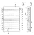
- FIG. 3 aprovides a simplified top view of a transformer integrated on a die.
- lines (conductors) 302 in FIG. 3 aare formed parallel to each other by standard silicon processing techniques.
- Magnetic material 304is deposited above and below parallel lines 302 , and around the leftmost and rightmost parallel lines to form a closed magnetic circuit (see FIG. 3 b ), so as to provide a large inductance and magnetic coupling among the lines. This increases magnetic coupling between the windings of the transformer for a given size of transformer.
- FIG. 3 ashows magnetic material 304 only above lines 302 .
- FIG. 3 bprovides a simplified cross-sectional view of a transformer according to embodiments of the present invention.
- Lines 302 in FIG. 3 bare insulated from each other and from magnetic material 304 by insulator 306 , which may be SiO 2 , for example.
- magnetic material 304 in FIG. 3 bis seen to be deposited both below and above lines 302 , as well as around the leftmost and rightmost lines.
- a small gapmay be fabricated between the top and bottom magnetic layers.
- FIG. 3 cshows a gap 306 in magnetic material 304 near the rightmost (with respect to the perspective view) line so that magnetic layer 306 does not completely surround lines 302 .
- Other embodimentsmay have a gap in the magnetic material near both the leftmost and rightmost lines. This results in a higher saturation current.
- the relative permeability of magnetic material 304may be greater than 100 and the relative permeability of insulator 306 may be close to one.
- FIGS. 3 a , 3 b , and 3 cshows only twelve parallel lines, and they do not show the die substrate, other layers, and interconnects.
- a simplified circuit model for the transformer of FIGS. 3 a and 3 b (or the embodiment of 3 c )is provided in FIG. 4 .
- the magnetic coupling between any two linesdecreases with increasing distance between the two lines.
- subsets of lines 302are used to form windings, where the lines belonging to any one subset of lines are connected in parallel to each other.
- one or more subsets of linesmay be connected in series with each other to form a winding of higher inductance. In either case, the windings thereby formed are smaller in number than the number of available lines.
- the subsets of lines 302are chosen such that no two lines belonging to any one subset are nearest neighbors. Another way of stating this is that lines that are nearest neighbors belong to different subsets. Two lines are said to be nearest neighbors when there are no other lines in between them.
- FIG. 5provides one example of a transformer having three windings formed from the twelve lines of FIG. 3 .
- a first windingis defined by the path between d 0 and c 0
- a second windingis defined by the path between d 1 and c 1
- a third windingis defined by the path between d 2 and c 2 .
- coupling coefficients between any two windings according to an embodiment of the present inventionare better when compared to an embodiment utilizing windings formed by connecting in parallel lines that are wider but fewer in number.
- the embodiment of FIG. 5provides better magnetic coupling than the case in which every four adjacent lines are combined into a wider line, where each wider line forms a winding.
- the linesare grouped into three subsets, where no two lines belonging to any one subset are nearest neighbors.
- Each subsetcorresponds to a unique winding.
- lines 302 b and 302 c in FIG. 5are nearest neighbors, but they do not belong to the same winding (subset).
- FIG. 6A simplified circuit model of FIG. 5 is shown in FIG. 6 .
- every third line in FIG. 5 starting from the leftmost lineis connected in parallel to form a first subset
- every third line starting from the first line to the right of the leftmost lineis connected in parallel to form a second subset
- every third line starting from the second line to the right of the leftmost lineis connected in parallel to form a third subset.
- i and mwill assume different values where m ⁇ i, and some of the subsets may be connected in series to form a winding.
- connections among the various lines making up the windingsmay be connected by way of another metal layer (not shown) above or below the lines, or may be made by starting and ending the lines on metal pads, and connecting the metal pads among each other by bonding wires or package traces to realize the desired windings.
- lines 302need not be linear or parallel.
- the phrase “A is connected to B”means that A and B are directly connected to each other by way of an interconnect, such as metal or polysilicon. This is to be distinguished from the phrase “A is coupled to B”, which means that the connection between A and B may not be direct. That is, there may be an active device or passive element between A and B.
Landscapes
- Engineering & Computer Science (AREA)
- Power Engineering (AREA)
- Multimedia (AREA)
- Physics & Mathematics (AREA)
- Electromagnetism (AREA)
- Coils Or Transformers For Communication (AREA)
- Soft Magnetic Materials (AREA)
- Semiconductor Integrated Circuits (AREA)
Abstract
Description
This application is a continuation of U.S. application Ser. No. 10/430,508, filed May 5, 2003 now U.S. Pat. No. 7,852,185, which is incorporated herein by reference in its entirety.
The present invention relates to transformers, and more particularly, to transformers that may be integrated on a die.
Transformers are used in many different types of power distribution systems, such as in switched voltage converters. An example of a switched voltage converter utilizing a transformer is the diagonal half-bridge flyback converter ofFIG. 1 . In a first portion of a switching cycle, bothtransistors transformer 106. All the diodes are OFF, i.e., reverse-biased. In a second (flyback) portion of a switching cycle, the energy previously stored in the transformer magnetic field is released to outputcapacitor 108 viaoutput diode 110. Any excess energy will be returned toinput capacitor 112 viainput diodes transistors Controller 118 adjusts the switching frequency to regulate the amount of energy provided to load120, so that the sensed voltage VS is close to reference voltage Vref. For a small load, the switching frequency is high. For a large load, the switching frequency is low. The coupling factor between the input and output windings oftransformer 106 determines how much of the stored magnetic energy is released to the output in the second (flyback) portion of switching cycle. Low coupling factor results in poor efficiency.
The flyback converter ofFIG. 1 is just one example of a switched voltage converter making use of a transformer. In many applications requiring a DC-to-DC converter, such as portable systems utilizing microprocessors, switched voltage converters may be more desirable than other types of voltage converters or regulators, such as linear voltage regulators, because they can be made more efficient. In a linear voltage regulator, the power conversion efficiency is always less than VS/VD, whereas in a switching converter, the efficiency is typically 80-95%.
Transformers find applications in power distribution systems other than the flyback converter, which is just one example. There are advantages to integrating a power distribution system on the same die as the circuits that are powered by the power distribution system. For example, as processor technology scales to smaller dimensions, supply voltages to circuits within a processor will also scale to smaller values. But for many processors, power consumption has also been increasing as technology progresses. Using an off-die voltage converter to provide a small supply voltage to a processor with a large power consumption leads to a large total electrical current being supplied to the processor. This can increase the electrical current per pin, or the total number of pins needed. Also, an increase in supply current can lead to an increase in resistive as well as inductive voltage drop across various off-die and on-die interconnects, and to a higher cost for decoupling capacitors. Integrating the voltage converter onto the die would mitigate these problems because a higher input voltage with lower current could be provided to the die by an off-die power supply, and the reduction of the higher input voltage to lower, regulated voltages could be done on the die closer to the circuits that require the regulated voltages.
Embodiments of the present invention may be integrated on a processor, or used in computer systems, such as that shown inFIG. 2 . InFIG. 2 , microprocessor die202 comprises many sub-blocks, such as arithmetic logic unit (ALU)204 and on-die cache 206.Microprocessor 202 may also communicate to other levels of cache, such as off-die cache 208. Higher memory hierarchy levels, such assystem memory 210, are accessed viahost bus 212 andchipset 214. In addition, other off-die functional units, such asgraphics accelerator 216 and network interface controller (NIC)218, to name just a few, may communicate withmicroprocessor 202 via appropriate busses or ports.
For a transformer to be small enough to be integrated on a die, it is proposed that its operating frequency, for example the frequency ofcontroller 108, be sufficiently high and that magnetic material suitable for high frequency operation be used to increase coupling between the windings of the transformer. For some embodiments, it is proposed that the magnetic material is chosen from the group consisting of amorphous CoZrTa, CoFeHfO, CoAlO, FeSiO, CoFeAlO, CoNbTa, CoZr, and other amorphous cobalt alloys. An amorphous alloy used in a particular embodiment may comprise various atomic percentages of its constituent elements. For example, a particular embodiment using the amorphous cobalt alloy CoZrTa may have 4% Zr, 4.5% Ta, with the rest being Co. For some other embodiments using CoZrTa, the range for Zr may be from 3% to 12% and the range for Ta may be from 0% to 10%. Other embodiments may use the cobalt alloy CoFeHfO, with 19.1% Fe, 14.5% Hf, and 22.1% O, or the Cobalt alloy CoFeAlO, with 51.1% Co, 21.9% Fe, and 27% Al. These merely serve as particular examples. The use of such magnetic material allows for operating frequencies of 10 MHz to 1 GHz, and higher. However, other magnetic material may be used in other embodiments.
The geometry or structure of a transformer according to embodiments of the present invention is illustrated inFIG. 3 a.FIG. 3 aprovides a simplified top view of a transformer integrated on a die. In one layer, lines (conductors)302 inFIG. 3 aare formed parallel to each other by standard silicon processing techniques.Magnetic material 304 is deposited above and belowparallel lines 302, and around the leftmost and rightmost parallel lines to form a closed magnetic circuit (seeFIG. 3 b), so as to provide a large inductance and magnetic coupling among the lines. This increases magnetic coupling between the windings of the transformer for a given size of transformer. For simplicity,FIG. 3 ashowsmagnetic material 304 only abovelines 302.
Insulatingmaterial 306 deposited aroundlines 302, and in any end gap inmagnetic material 304 if present, should have a smaller magnetic permeability than that ofmagnetic material 304. Otherwise, the magnetic coupling between the lines may degrade. For example, the relative permeability ofmagnetic material 304 may be greater than 100 and the relative permeability ofinsulator 306 may be close to one.
Forminglines 302 within one layer, as shown in the embodiment ofFIGS. 3 a,3band3c, reduces the number of metal levels needed, and reduces capacitance betweenlines 302 when compared to forming lines on top of each other.
For simplicity,FIGS. 3 a,3b, and3cshows only twelve parallel lines, and they do not show the die substrate, other layers, and interconnects. A simplified circuit model for the transformer ofFIGS. 3 aand3b(or the embodiment of3c) is provided inFIG. 4 . The magnetic coupling between any two lines decreases with increasing distance between the two lines.
According to embodiments of the present invention, subsets oflines 302 are used to form windings, where the lines belonging to any one subset of lines are connected in parallel to each other. For some embodiments, there is a one-to-one correspondence between a subset and a winding. That is, each subset of parallel connected lines forms a unique transformer winding. For other embodiments, one or more subsets of lines may be connected in series with each other to form a winding of higher inductance. In either case, the windings thereby formed are smaller in number than the number of available lines. The subsets oflines 302 are chosen such that no two lines belonging to any one subset are nearest neighbors. Another way of stating this is that lines that are nearest neighbors belong to different subsets. Two lines are said to be nearest neighbors when there are no other lines in between them.
As an example of connecting lines to form the windings of a transformer,FIG. 5 provides one example of a transformer having three windings formed from the twelve lines ofFIG. 3 . A first winding is defined by the path between d0and c0, a second winding is defined by the path between d1and c1, and a third winding is defined by the path between d2and c2. It has been found by simulation that coupling coefficients among any two of the three windings in a transformer according to an embodiment of the present invention may be as high as 95%, and in some cases, higher than 98%, despite the fact that the coupling of any two individual lines may be as poor as 10%. It has also been found that coupling coefficients between any two windings according to an embodiment of the present invention are better when compared to an embodiment utilizing windings formed by connecting in parallel lines that are wider but fewer in number. For example, for a given area, the embodiment ofFIG. 5 provides better magnetic coupling than the case in which every four adjacent lines are combined into a wider line, where each wider line forms a winding.
As seen inFIG. 5 , the lines are grouped into three subsets, where no two lines belonging to any one subset are nearest neighbors. Each subset corresponds to a unique winding. For example, lines302band302cinFIG. 5 are nearest neighbors, but they do not belong to the same winding (subset). A simplified circuit model ofFIG. 5 is shown inFIG. 6 . In particular, every third line inFIG. 5 starting from the leftmost line is connected in parallel to form a first subset, every third line starting from the first line to the right of the leftmost line is connected in parallel to form a second subset, and every third line starting from the second line to the right of the leftmost line is connected in parallel to form a third subset. This approach to choosing subsets of parallel connected lines may be generalized to an arbitrary number of lines as follows: For an arbitrary number of lines n>1, denoted as line(i), i=0, 1, . . . , n−1, choose m>1 subsets, denoted as subset(j), j=0, 1, . . . , m−1, where for each i=0, 1, . . . , n−1, line(i) belongs to subset(i modulo m), where all the lines in any one subset are connected in parallel to each other.
Note that the latter expression is more narrow than the earlier stated property that no two lines belonging to any one subset are nearest neighbors. That is, if line(i) belongs to subset(i modulo m) for each i, then no two lines belonging to any one subset are nearest neighbors. However, the converse is not necessarily true.
In the case ofFIG. 5 , i=12 and m=3, and each subset corresponds to a unique winding. For other embodiments, i and m will assume different values where m<i, and some of the subsets may be connected in series to form a winding.
The connections among the various lines making up the windings may be connected by way of another metal layer (not shown) above or below the lines, or may be made by starting and ending the lines on metal pads, and connecting the metal pads among each other by bonding wires or package traces to realize the desired windings.
Various modifications may be made to the disclosed embodiments without departing from the scope of the invention as claimed below. For example, in some embodiments,lines 302 need not be linear or parallel. Furthermore, it is to be understood in these letters patent that the phrase “A is connected to B” means that A and B are directly connected to each other by way of an interconnect, such as metal or polysilicon. This is to be distinguished from the phrase “A is coupled to B”, which means that the connection between A and B may not be direct. That is, there may be an active device or passive element between A and B.
Claims (20)
1. A die comprising:
a transformer including windings formed from a set of lines, the lines formed within one layer on the die, wherein the lines are arranged in parallel with each other, and no two lines in the set of lines belonging to any one winding among the windings are nearest neighbors.
2. The die ofclaim 1 , further comprising a magnetic material located near the set of lines, wherein the magnetic material includes an alloy of cobalt.
3. The die ofclaim 1 , further comprising a magnetic material located near the set of lines, wherein the magnetic material includes CoZrTa.
4. The die ofclaim 1 , further comprising a magnetic material located near the set of lines, wherein the magnetic material includes CoZrTa, CoFeHfO, CoAlO, FeSiO, CoFeAlO, CoNbTa, or CoZr.
5. The die ofclaim 1 , wherein the set of lines includes n>1 lines denoted as line(i), i=0, 1, . . . , n−1, and the transformer includes m>1 windings denoted as winding (j), j=0, 1, . . . , m−1, wherein line(i) belongs to winding(i modulo m).
6. The die ofclaim 1 , further comprising a magnetic material surrounding the set of lines except for the ends of the set of lines.
7. The die ofclaim 1 , further comprising a magnetic material surrounding the set of lines except for ends of the set of lines and except for a gap near the rightmost line in the set of lines.
8. A die comprising:
lines formed within one layer of the die, the lines arranged to form windings of a transformer, wherein two lines that are nearest neighbors belong to two different windings, and no two lines in the lines belonging to any winding among the windings are nearest neighbors.
9. A die comprising:
lines formed within one layer of the die, the lines arranged to form windings of a transformer, wherein two lines that are nearest neighbors belong to two different windings, wherein a number of the windings is equal to a number of the lines.
10. The die ofclaim 8 , further comprising a magnetic material located near the lines, wherein the magnetic material includes CoFeHfO.
11. The die ofclaim 10 , wherein the magnetic material is located below and above the lines.
12. The die ofclaim 11 , further comprising an insulator, such that the lines are insulated from the each other by the insulator.
13. A die comprising:
lines arranged in parallel with each other and formed within one layer of the die, the lines arranged in sub-sets to form windings of a transformer, each of the sub-sets including at least one of the lines to form one of the windings, and no two lines in the set of lines belonging to any one winding among the windings are nearest neighbors; and
a controller coupled the transformer.
14. The die ofclaim 13 , wherein the controller is to operate the transformer at a frequency greater than 10 MHz.
15. A die comprising:
lines arranged in parallel with each other and formed within one layer of the die, the lines arranged in sub-sets to form windings of a transformer, each of the sub-sets including at least one of the lines to form one of the windings, wherein no two lines in each of the windings are nearest neighbors: and
a controller coupled the transformer.
16. The die ofclaim 13 , wherein at least one of the windings is formed from at least two different lines of one of the sub-sets.
17. The die ofclaim 13 , wherein a number of the windings is less than a number of the lines.
18. The die ofclaim 13 , further comprising a magnetic material located near the lines, wherein the magnetic material includes CoAlO.
19. The die ofclaim 18 , wherein the magnetic material is located on at least one side of the lines.
20. The die ofclaim 19 , further comprising an insulator located between the lines and the magnetic material.
Priority Applications (1)
| Application Number | Priority Date | Filing Date | Title |
|---|---|---|---|
| US12/955,415US8471667B2 (en) | 2003-05-05 | 2010-11-29 | On-die micro-transformer structures with magnetic materials |
Applications Claiming Priority (2)
| Application Number | Priority Date | Filing Date | Title |
|---|---|---|---|
| US10/430,508US7852185B2 (en) | 2003-05-05 | 2003-05-05 | On-die micro-transformer structures with magnetic materials |
| US12/955,415US8471667B2 (en) | 2003-05-05 | 2010-11-29 | On-die micro-transformer structures with magnetic materials |
Related Parent Applications (1)
| Application Number | Title | Priority Date | Filing Date |
|---|---|---|---|
| US10/430,508ContinuationUS7852185B2 (en) | 2003-05-05 | 2003-05-05 | On-die micro-transformer structures with magnetic materials |
Publications (2)
| Publication Number | Publication Date |
|---|---|
| US20110068887A1 US20110068887A1 (en) | 2011-03-24 |
| US8471667B2true US8471667B2 (en) | 2013-06-25 |
Family
ID=33416255
Family Applications (2)
| Application Number | Title | Priority Date | Filing Date |
|---|---|---|---|
| US10/430,508Expired - Fee RelatedUS7852185B2 (en) | 2003-05-05 | 2003-05-05 | On-die micro-transformer structures with magnetic materials |
| US12/955,415Expired - Fee RelatedUS8471667B2 (en) | 2003-05-05 | 2010-11-29 | On-die micro-transformer structures with magnetic materials |
Family Applications Before (1)
| Application Number | Title | Priority Date | Filing Date |
|---|---|---|---|
| US10/430,508Expired - Fee RelatedUS7852185B2 (en) | 2003-05-05 | 2003-05-05 | On-die micro-transformer structures with magnetic materials |
Country Status (3)
| Country | Link |
|---|---|
| US (2) | US7852185B2 (en) |
| TW (1) | TWI341043B (en) |
| WO (1) | WO2004100194A2 (en) |
Cited By (1)
| Publication number | Priority date | Publication date | Assignee | Title |
|---|---|---|---|---|
| US9124174B2 (en) | 2005-06-30 | 2015-09-01 | Micron Technology, Inc. | DC-DC converter switching transistor current measurement technique |
Families Citing this family (11)
| Publication number | Priority date | Publication date | Assignee | Title |
|---|---|---|---|---|
| US6856006B2 (en)* | 2002-03-28 | 2005-02-15 | Siliconix Taiwan Ltd | Encapsulation method and leadframe for leadless semiconductor packages |
| US7852185B2 (en)* | 2003-05-05 | 2010-12-14 | Intel Corporation | On-die micro-transformer structures with magnetic materials |
| US7436277B2 (en) | 2005-06-01 | 2008-10-14 | Intel Corporation | Power transformer |
| CN101283449B (en)* | 2005-07-01 | 2014-08-20 | 维税-希力康克斯公司 | Complete power management system implemented in a single surface mount package |
| US20080157911A1 (en)* | 2006-12-29 | 2008-07-03 | Fajardo Arnel M | Soft magnetic layer for on-die inductively coupled wires with high electrical resistance |
| WO2009082706A1 (en) | 2007-12-21 | 2009-07-02 | The Trustees Of Columbia University In The City Of New York | Active cmos sensor array for electrochemical biomolecular detection |
| US8436707B2 (en)* | 2010-01-12 | 2013-05-07 | Infineon Technologies Ag | System and method for integrated inductor |
| US8513771B2 (en) | 2010-06-07 | 2013-08-20 | Infineon Technologies Ag | Semiconductor package with integrated inductor |
| WO2013032753A2 (en)* | 2011-08-26 | 2013-03-07 | The Trustees Of Columbia University In The City Of New York | Systems and methods for switched-inductor integrated voltage regulators |
| US9124173B2 (en) | 2012-08-20 | 2015-09-01 | International Business Machines Corporation | Slab inductor device providing efficient on-chip supply voltage conversion and regulation |
| US20180197676A1 (en)* | 2017-01-10 | 2018-07-12 | General Electric Company | Insulation for tranformer or inductor |
Citations (81)
| Publication number | Priority date | Publication date | Assignee | Title |
|---|---|---|---|---|
| US3607462A (en) | 1968-03-21 | 1971-09-21 | Spang Ind Inc | Process of magnetic particle preparation |
| US3881244A (en) | 1972-06-02 | 1975-05-06 | Texas Instruments Inc | Method of making a solid state inductor |
| US3905883A (en) | 1973-06-20 | 1975-09-16 | Hitachi Ltd | Electrolytic etching method |
| FR2369694A1 (en) | 1976-10-29 | 1978-05-26 | Cit Alcatel | Transformer for use at 20 MHZ - has two adjacent waveforms formed of conductive alloy on substrate |
| US4543553A (en) | 1983-05-18 | 1985-09-24 | Murata Manufacturing Co., Ltd. | Chip-type inductor |
| JPS6120311A (en) | 1984-07-09 | 1986-01-29 | Nippon Telegr & Teleph Corp <Ntt> | Fabrication of amorphous soft magnetic film |
| EP0295028A1 (en) | 1987-06-08 | 1988-12-14 | Esselte Meto International GmbH | Magnetic devices |
| US4791719A (en) | 1983-12-22 | 1988-12-20 | Hitachi, Ltd. | Method of manufacturing a thin-film magnetic head |
| US4797648A (en) | 1987-03-09 | 1989-01-10 | Murata Manufacturing Co., Ltd. | Chip inductor |
| US4816784A (en) | 1988-01-19 | 1989-03-28 | Northern Telecom Limited | Balanced planar transformers |
| US4884156A (en) | 1984-01-26 | 1989-11-28 | Canon Kabushiki Kaisha | Magnetic head having a thin-film and a coil |
| US4959631A (en) | 1987-09-29 | 1990-09-25 | Kabushiki Kaisha Toshiba | Planar inductor |
| US5047296A (en) | 1987-09-18 | 1991-09-10 | Commissariat A L'energie Atomique | Composite magnetic material and its production process |
| JPH03214411A (en) | 1990-01-19 | 1991-09-19 | Canon Inc | Thin-film magnetic head |
| US5053697A (en) | 1989-06-16 | 1991-10-01 | Schlumberger Industries | Input circuit for an electrical energy meter |
| DE4117878A1 (en) | 1990-05-31 | 1991-12-12 | Toshiba Kawasaki Kk | Miniature planar magnetic element e.g. induction coil or transformer - is formed by layers of insulating and magnetic material on either side of coil |
| US5095357A (en) | 1989-08-18 | 1992-03-10 | Mitsubishi Denki Kabushiki Kaisha | Inductive structures for semiconductor integrated circuits |
| US5121852A (en) | 1990-05-23 | 1992-06-16 | Essef Corporation | Dynamic pressure relief seal for pressure vessels |
| US5169713A (en) | 1990-02-22 | 1992-12-08 | Commissariat A L'energie Atomique | High frequency electromagnetic radiation absorbent coating comprising a binder and chips obtained from a laminate of alternating amorphous magnetic films and electrically insulating |
| US5221459A (en) | 1992-02-12 | 1993-06-22 | Nkk Corporation | Method of manufacturing a magnetic disk substrate of titanium |
| US5298857A (en) | 1992-04-06 | 1994-03-29 | Landis & Gyr Metering, Inc. | Electrical energy meter with a precision integrator for current measurement |
| JPH06124843A (en) | 1992-10-14 | 1994-05-06 | Nippon Telegr & Teleph Corp <Ntt> | High frequency thin film transformer |
| US5420558A (en) | 1992-05-27 | 1995-05-30 | Fuji Electric Co., Ltd. | Thin film transformer |
| US5446311A (en) | 1994-09-16 | 1995-08-29 | International Business Machines Corporation | High-Q inductors in silicon technology without expensive metalization |
| JPH07272932A (en) | 1994-03-31 | 1995-10-20 | Canon Inc | Printed inductor |
| US5469399A (en) | 1993-03-16 | 1995-11-21 | Kabushiki Kaisha Toshiba | Semiconductor memory, memory card, and method of driving power supply for EEPROM |
| US5530415A (en) | 1989-08-01 | 1996-06-25 | Tdk Corporation | Composite winding type stacked-layer inductors including self inductive inductors and manual-inductive inductors |
| EP0725407A1 (en) | 1995-02-03 | 1996-08-07 | International Business Machines Corporation | Three-dimensional integrated circuit inductor |
| US5609946A (en) | 1995-10-03 | 1997-03-11 | General Electric Company | High frequency, high density, low profile, magnetic circuit components |
| US5635892A (en) | 1994-12-06 | 1997-06-03 | Lucent Technologies Inc. | High Q integrated inductor |
| US5694030A (en) | 1993-03-15 | 1997-12-02 | Kabushiki Kaisha Toshiba | Magnetic element for power supply and DC-to-DC converter |
| US5696441A (en) | 1994-05-13 | 1997-12-09 | Distribution Control Systems, Inc. | Linear alternating current interface for electronic meters |
| US5705287A (en) | 1994-09-20 | 1998-01-06 | International Business Machines Corporation | Magnetic recording disk with metal nitride texturing layer |
| US5781071A (en) | 1994-12-17 | 1998-07-14 | Sony Corporation | Transformers and amplifiers |
| US5801100A (en) | 1997-03-07 | 1998-09-01 | Industrial Technology Research Institute | Electroless copper plating method for forming integrated circuit structures |
| US5834825A (en) | 1995-12-27 | 1998-11-10 | Nec Corporation | Semiconductor device having spiral wiring directly covered with an insulating layer containing ferromagnetic particles |
| EP0884783A2 (en) | 1997-06-10 | 1998-12-16 | Lucent Technologies Inc. | A micromagnetic device for power processing applications and method of manufacture therefor |
| US5877533A (en) | 1993-05-21 | 1999-03-02 | Semiconductor Energy Laboratory Co., Ltd. | Hybrid integrated circuit component |
| US5892425A (en) | 1997-04-10 | 1999-04-06 | Virginia Tech Intellectual Properties, Inc. | Interwound center-tapped spiral inductor |
| US5920979A (en) | 1996-04-15 | 1999-07-13 | Read-Rite Corporation | Method of forming an inductive magnetic head with approximate zero magnetostriction |
| US5930415A (en) | 1996-10-14 | 1999-07-27 | Gec Alsthom T & D Sa | Monitoring device for a gas-insulated cable |
| US5952704A (en) | 1996-12-06 | 1999-09-14 | Electronics And Telecommunications Research Institute | Inductor devices using substrate biasing technique |
| US5961746A (en) | 1996-04-22 | 1999-10-05 | Read-Rite Corporation | Corrosion resistant amorphous magnetic alloys |
| US5976715A (en) | 1996-02-02 | 1999-11-02 | Lucent Techologies Inc. | Articles comprising magnetically soft thin films |
| US6031445A (en) | 1997-11-28 | 2000-02-29 | Stmicroelectronics S.A. | Transformer for integrated circuits |
| US6033782A (en) | 1993-08-13 | 2000-03-07 | General Atomics | Low volume lightweight magnetodielectric materials |
| US6037649A (en) | 1999-04-01 | 2000-03-14 | Winbond Electronics Corp. | Three-dimension inductor structure in integrated circuit technology |
| JP2000082621A (en) | 1998-09-07 | 2000-03-21 | Fuji Electric Co Ltd | Plane transformer |
| US6040226A (en) | 1997-05-27 | 2000-03-21 | General Electric Company | Method for fabricating a thin film inductor |
| US6043641A (en) | 1998-02-17 | 2000-03-28 | Singer; Jerome R. | Method and apparatus for rapid determinations of voltage and current in wires and conductors |
| TW386310B (en) | 1998-10-30 | 2000-04-01 | Chiou Jing Hung | Method of producing microinductor and structure thereof |
| US6067002A (en) | 1995-09-12 | 2000-05-23 | Murata Manufacturing Co., Ltd. | Circuit substrate with a built-in coil |
| US6103136A (en) | 1998-03-23 | 2000-08-15 | Headway Technologies, Inc. | Method for forming a soft adjacent layer (SAL) magnetoresistive (MR) sensor element with transversely magnetically biased soft adjacent layer (SAL) |
| US6114937A (en) | 1996-08-23 | 2000-09-05 | International Business Machines Corporation | Integrated circuit spiral inductor |
| US6121852A (en) | 1997-07-15 | 2000-09-19 | Kabushiki Kaisha Toshiba | Distributed constant element using a magnetic thin film |
| TW411481B (en) | 1998-03-24 | 2000-11-11 | Ericsson Telefon Ab L M | An inductance device |
| US6166422A (en) | 1998-05-13 | 2000-12-26 | Lsi Logic Corporation | Inductor with cobalt/nickel core for integrated circuit structure with high inductance and high Q-factor |
| US6191495B1 (en) | 1997-06-10 | 2001-02-20 | Lucent Technologies Inc. | Micromagnetic device having an anisotropic ferromagnetic core and method of manufacture therefor |
| US6201287B1 (en) | 1998-10-26 | 2001-03-13 | Micron Technology, Inc. | Monolithic inductance-enhancing integrated circuits, complementary metal oxide semiconductor (CMOS) inductance-enhancing integrated circuits, inductor assemblies, and inductance-multiplying methods |
| US6207303B1 (en) | 1997-07-03 | 2001-03-27 | Kabushiki Kaisha Toshiba | Multilayered magnetic film having buffer layer inserted between resin layer and laminated magnetic film layer and thin film inductor using the same |
| WO2001039220A1 (en) | 1999-11-23 | 2001-05-31 | Intel Corporation | Inductor for integrated circuit and methods of manufacture |
| US6240621B1 (en) | 1997-08-05 | 2001-06-05 | U.S. Philips Corporation | Method of manufacturing a plurality of electronic components |
| US6281560B1 (en) | 1995-10-10 | 2001-08-28 | Georgia Tech Research Corp. | Microfabricated electromagnetic system and method for forming electromagnets in microfabricated devices |
| US6291305B1 (en) | 1999-06-11 | 2001-09-18 | S3 Graphics Co., Ltd. | Method for implementing resistance, capacitance and/or inductance in an integrated circuit |
| JP3214411B2 (en) | 1997-09-19 | 2001-10-02 | 三菱電機株式会社 | Electronics |
| US20010052837A1 (en) | 1999-02-24 | 2001-12-20 | Walsh Joseph G. | Planar miniature inductors and transformers |
| US6392524B1 (en) | 2000-06-09 | 2002-05-21 | Xerox Corporation | Photolithographically-patterned out-of-plane coil structures and method of making |
| US6433299B1 (en) | 1991-09-11 | 2002-08-13 | American Research Corporation Of Virginia | Monolithic magnetic modules for integrated planar magnetic circuitry and process for manufacturing same |
| WO2002065492A2 (en) | 2001-01-19 | 2002-08-22 | Intel Corporation | Integrated transformer |
| US6441715B1 (en) | 1999-02-17 | 2002-08-27 | Texas Instruments Incorporated | Method of fabricating a miniaturized integrated circuit inductor and transformer fabrication |
| US20030001709A1 (en) | 2001-06-29 | 2003-01-02 | Visser Hendrik Arend | Multiple-interleaved integrated circuit transformer |
| US6583620B2 (en)* | 2000-07-21 | 2003-06-24 | Delta Tooling Co., Ltd. | Plane magnetic sensor and plane magnetic sensor for multidimensional magnetic field analysis |
| US6597593B1 (en) | 2000-07-12 | 2003-07-22 | Sun Microsystems, Inc. | Powering IC chips using AC signals |
| US20040246226A1 (en) | 2003-05-23 | 2004-12-09 | Seung-Hwan Moon | Inverter and liquid crystal display including inverter |
| US6838863B2 (en) | 2002-12-30 | 2005-01-04 | Intel Corporation | Voltage converter utilizing independently switched inductors |
| US6856228B2 (en) | 1999-11-23 | 2005-02-15 | Intel Corporation | Integrated inductor |
| US6891461B2 (en) | 1999-11-23 | 2005-05-10 | Intel Corporation | Integrated transformer |
| US20060091896A1 (en) | 2004-10-29 | 2006-05-04 | Gerhard Schrom | Method and apparatus for measuring coil current |
| US20070001762A1 (en) | 2005-06-30 | 2007-01-04 | Gerhard Schrom | DC-DC converter switching transistor current measurement technique |
| US7852185B2 (en) | 2003-05-05 | 2010-12-14 | Intel Corporation | On-die micro-transformer structures with magnetic materials |
| JP5081615B2 (en) | 2004-03-16 | 2012-11-28 | イプセン ファルマ ソシエテ パール アクシオン サンプリフィエ | Use of catalyst system for (co) oligopolymerization of lactide and glycolide |
Family Cites Families (4)
| Publication number | Priority date | Publication date | Assignee | Title |
|---|---|---|---|---|
| US520837A (en)* | 1894-06-05 | price | ||
| JPH0581615A (en) | 1991-09-24 | 1993-04-02 | Sharp Corp | Production of thin-film magnetic head |
| DE9301111U1 (en)* | 1993-01-27 | 1994-06-01 | Lucas Industries P.L.C., Birmingham, West Midlands | Arrangement for torque measurements on motor vehicles |
| US20100052837A1 (en)* | 2008-09-03 | 2010-03-04 | Siqi Fan | Integrated Circuit Multilevel Inductor |
- 2003
- 2003-05-05USUS10/430,508patent/US7852185B2/ennot_activeExpired - Fee Related
- 2004
- 2004-04-14WOPCT/US2004/011420patent/WO2004100194A2/enactiveApplication Filing
- 2004-04-22TWTW093111253Apatent/TWI341043B/ennot_activeIP Right Cessation
- 2010
- 2010-11-29USUS12/955,415patent/US8471667B2/ennot_activeExpired - Fee Related
Patent Citations (90)
| Publication number | Priority date | Publication date | Assignee | Title |
|---|---|---|---|---|
| US3607462A (en) | 1968-03-21 | 1971-09-21 | Spang Ind Inc | Process of magnetic particle preparation |
| US3881244A (en) | 1972-06-02 | 1975-05-06 | Texas Instruments Inc | Method of making a solid state inductor |
| US3905883A (en) | 1973-06-20 | 1975-09-16 | Hitachi Ltd | Electrolytic etching method |
| FR2369694A1 (en) | 1976-10-29 | 1978-05-26 | Cit Alcatel | Transformer for use at 20 MHZ - has two adjacent waveforms formed of conductive alloy on substrate |
| US4543553A (en) | 1983-05-18 | 1985-09-24 | Murata Manufacturing Co., Ltd. | Chip-type inductor |
| US4791719A (en) | 1983-12-22 | 1988-12-20 | Hitachi, Ltd. | Method of manufacturing a thin-film magnetic head |
| US4884156A (en) | 1984-01-26 | 1989-11-28 | Canon Kabushiki Kaisha | Magnetic head having a thin-film and a coil |
| JPS6120311A (en) | 1984-07-09 | 1986-01-29 | Nippon Telegr & Teleph Corp <Ntt> | Fabrication of amorphous soft magnetic film |
| US4797648A (en) | 1987-03-09 | 1989-01-10 | Murata Manufacturing Co., Ltd. | Chip inductor |
| EP0295028A1 (en) | 1987-06-08 | 1988-12-14 | Esselte Meto International GmbH | Magnetic devices |
| US5047296A (en) | 1987-09-18 | 1991-09-10 | Commissariat A L'energie Atomique | Composite magnetic material and its production process |
| US4959631A (en) | 1987-09-29 | 1990-09-25 | Kabushiki Kaisha Toshiba | Planar inductor |
| US4816784A (en) | 1988-01-19 | 1989-03-28 | Northern Telecom Limited | Balanced planar transformers |
| US5053697A (en) | 1989-06-16 | 1991-10-01 | Schlumberger Industries | Input circuit for an electrical energy meter |
| US5530415A (en) | 1989-08-01 | 1996-06-25 | Tdk Corporation | Composite winding type stacked-layer inductors including self inductive inductors and manual-inductive inductors |
| US5095357A (en) | 1989-08-18 | 1992-03-10 | Mitsubishi Denki Kabushiki Kaisha | Inductive structures for semiconductor integrated circuits |
| JPH03214411A (en) | 1990-01-19 | 1991-09-19 | Canon Inc | Thin-film magnetic head |
| US5169713A (en) | 1990-02-22 | 1992-12-08 | Commissariat A L'energie Atomique | High frequency electromagnetic radiation absorbent coating comprising a binder and chips obtained from a laminate of alternating amorphous magnetic films and electrically insulating |
| US5121852A (en) | 1990-05-23 | 1992-06-16 | Essef Corporation | Dynamic pressure relief seal for pressure vessels |
| DE4117878A1 (en) | 1990-05-31 | 1991-12-12 | Toshiba Kawasaki Kk | Miniature planar magnetic element e.g. induction coil or transformer - is formed by layers of insulating and magnetic material on either side of coil |
| US6404317B1 (en) | 1990-05-31 | 2002-06-11 | Kabushiki Kaisha Toshiba | Planar magnetic element |
| US6593841B1 (en) | 1990-05-31 | 2003-07-15 | Kabushiki Kaisha Toshiba | Planar magnetic element |
| US5583474A (en) | 1990-05-31 | 1996-12-10 | Kabushiki Kaisha Toshiba | Planar magnetic element |
| US6433299B1 (en) | 1991-09-11 | 2002-08-13 | American Research Corporation Of Virginia | Monolithic magnetic modules for integrated planar magnetic circuitry and process for manufacturing same |
| US5221459A (en) | 1992-02-12 | 1993-06-22 | Nkk Corporation | Method of manufacturing a magnetic disk substrate of titanium |
| US5298857A (en) | 1992-04-06 | 1994-03-29 | Landis & Gyr Metering, Inc. | Electrical energy meter with a precision integrator for current measurement |
| US5420558A (en) | 1992-05-27 | 1995-05-30 | Fuji Electric Co., Ltd. | Thin film transformer |
| JPH06124843A (en) | 1992-10-14 | 1994-05-06 | Nippon Telegr & Teleph Corp <Ntt> | High frequency thin film transformer |
| US5694030A (en) | 1993-03-15 | 1997-12-02 | Kabushiki Kaisha Toshiba | Magnetic element for power supply and DC-to-DC converter |
| US5469399A (en) | 1993-03-16 | 1995-11-21 | Kabushiki Kaisha Toshiba | Semiconductor memory, memory card, and method of driving power supply for EEPROM |
| US5877533A (en) | 1993-05-21 | 1999-03-02 | Semiconductor Energy Laboratory Co., Ltd. | Hybrid integrated circuit component |
| US6033782A (en) | 1993-08-13 | 2000-03-07 | General Atomics | Low volume lightweight magnetodielectric materials |
| JPH07272932A (en) | 1994-03-31 | 1995-10-20 | Canon Inc | Printed inductor |
| US5696441A (en) | 1994-05-13 | 1997-12-09 | Distribution Control Systems, Inc. | Linear alternating current interface for electronic meters |
| US5446311A (en) | 1994-09-16 | 1995-08-29 | International Business Machines Corporation | High-Q inductors in silicon technology without expensive metalization |
| US5705287A (en) | 1994-09-20 | 1998-01-06 | International Business Machines Corporation | Magnetic recording disk with metal nitride texturing layer |
| US5635892A (en) | 1994-12-06 | 1997-06-03 | Lucent Technologies Inc. | High Q integrated inductor |
| US5781071A (en) | 1994-12-17 | 1998-07-14 | Sony Corporation | Transformers and amplifiers |
| EP0725407A1 (en) | 1995-02-03 | 1996-08-07 | International Business Machines Corporation | Three-dimensional integrated circuit inductor |
| US6067002A (en) | 1995-09-12 | 2000-05-23 | Murata Manufacturing Co., Ltd. | Circuit substrate with a built-in coil |
| US5609946A (en) | 1995-10-03 | 1997-03-11 | General Electric Company | High frequency, high density, low profile, magnetic circuit components |
| US6281560B1 (en) | 1995-10-10 | 2001-08-28 | Georgia Tech Research Corp. | Microfabricated electromagnetic system and method for forming electromagnets in microfabricated devices |
| US5834825A (en) | 1995-12-27 | 1998-11-10 | Nec Corporation | Semiconductor device having spiral wiring directly covered with an insulating layer containing ferromagnetic particles |
| US5976715A (en) | 1996-02-02 | 1999-11-02 | Lucent Techologies Inc. | Articles comprising magnetically soft thin films |
| US5920979A (en) | 1996-04-15 | 1999-07-13 | Read-Rite Corporation | Method of forming an inductive magnetic head with approximate zero magnetostriction |
| US5961746A (en) | 1996-04-22 | 1999-10-05 | Read-Rite Corporation | Corrosion resistant amorphous magnetic alloys |
| US6114937A (en) | 1996-08-23 | 2000-09-05 | International Business Machines Corporation | Integrated circuit spiral inductor |
| US5930415A (en) | 1996-10-14 | 1999-07-27 | Gec Alsthom T & D Sa | Monitoring device for a gas-insulated cable |
| US5952704A (en) | 1996-12-06 | 1999-09-14 | Electronics And Telecommunications Research Institute | Inductor devices using substrate biasing technique |
| US5801100A (en) | 1997-03-07 | 1998-09-01 | Industrial Technology Research Institute | Electroless copper plating method for forming integrated circuit structures |
| US5892425A (en) | 1997-04-10 | 1999-04-06 | Virginia Tech Intellectual Properties, Inc. | Interwound center-tapped spiral inductor |
| US6040226A (en) | 1997-05-27 | 2000-03-21 | General Electric Company | Method for fabricating a thin film inductor |
| US6191495B1 (en) | 1997-06-10 | 2001-02-20 | Lucent Technologies Inc. | Micromagnetic device having an anisotropic ferromagnetic core and method of manufacture therefor |
| EP0884783A2 (en) | 1997-06-10 | 1998-12-16 | Lucent Technologies Inc. | A micromagnetic device for power processing applications and method of manufacture therefor |
| US6207303B1 (en) | 1997-07-03 | 2001-03-27 | Kabushiki Kaisha Toshiba | Multilayered magnetic film having buffer layer inserted between resin layer and laminated magnetic film layer and thin film inductor using the same |
| US6414564B1 (en) | 1997-07-15 | 2002-07-02 | Kabushiki Kaisha Toshiba | Distributed constant element using a magnetic thin film |
| US6121852A (en) | 1997-07-15 | 2000-09-19 | Kabushiki Kaisha Toshiba | Distributed constant element using a magnetic thin film |
| US6240621B1 (en) | 1997-08-05 | 2001-06-05 | U.S. Philips Corporation | Method of manufacturing a plurality of electronic components |
| JP3214411B2 (en) | 1997-09-19 | 2001-10-02 | 三菱電機株式会社 | Electronics |
| US6031445A (en) | 1997-11-28 | 2000-02-29 | Stmicroelectronics S.A. | Transformer for integrated circuits |
| US6043641A (en) | 1998-02-17 | 2000-03-28 | Singer; Jerome R. | Method and apparatus for rapid determinations of voltage and current in wires and conductors |
| US6103136A (en) | 1998-03-23 | 2000-08-15 | Headway Technologies, Inc. | Method for forming a soft adjacent layer (SAL) magnetoresistive (MR) sensor element with transversely magnetically biased soft adjacent layer (SAL) |
| US6194987B1 (en) | 1998-03-24 | 2001-02-27 | Telefonaktiebolaget Lm Ericsson | Inductance device |
| TW411481B (en) | 1998-03-24 | 2000-11-11 | Ericsson Telefon Ab L M | An inductance device |
| US6166422A (en) | 1998-05-13 | 2000-12-26 | Lsi Logic Corporation | Inductor with cobalt/nickel core for integrated circuit structure with high inductance and high Q-factor |
| JP2000082621A (en) | 1998-09-07 | 2000-03-21 | Fuji Electric Co Ltd | Plane transformer |
| US6201287B1 (en) | 1998-10-26 | 2001-03-13 | Micron Technology, Inc. | Monolithic inductance-enhancing integrated circuits, complementary metal oxide semiconductor (CMOS) inductance-enhancing integrated circuits, inductor assemblies, and inductance-multiplying methods |
| TW386310B (en) | 1998-10-30 | 2000-04-01 | Chiou Jing Hung | Method of producing microinductor and structure thereof |
| US6441715B1 (en) | 1999-02-17 | 2002-08-27 | Texas Instruments Incorporated | Method of fabricating a miniaturized integrated circuit inductor and transformer fabrication |
| US20010052837A1 (en) | 1999-02-24 | 2001-12-20 | Walsh Joseph G. | Planar miniature inductors and transformers |
| US6037649A (en) | 1999-04-01 | 2000-03-14 | Winbond Electronics Corp. | Three-dimension inductor structure in integrated circuit technology |
| US6291305B1 (en) | 1999-06-11 | 2001-09-18 | S3 Graphics Co., Ltd. | Method for implementing resistance, capacitance and/or inductance in an integrated circuit |
| WO2001039220A1 (en) | 1999-11-23 | 2001-05-31 | Intel Corporation | Inductor for integrated circuit and methods of manufacture |
| US6891461B2 (en) | 1999-11-23 | 2005-05-10 | Intel Corporation | Integrated transformer |
| US6452247B1 (en) | 1999-11-23 | 2002-09-17 | Intel Corporation | Inductor for integrated circuit |
| US20030001713A1 (en) | 1999-11-23 | 2003-01-02 | Gardner Donald S. | Integrated transformer |
| US6870456B2 (en) | 1999-11-23 | 2005-03-22 | Intel Corporation | Integrated transformer |
| US6856228B2 (en) | 1999-11-23 | 2005-02-15 | Intel Corporation | Integrated inductor |
| US6392524B1 (en) | 2000-06-09 | 2002-05-21 | Xerox Corporation | Photolithographically-patterned out-of-plane coil structures and method of making |
| US6597593B1 (en) | 2000-07-12 | 2003-07-22 | Sun Microsystems, Inc. | Powering IC chips using AC signals |
| US6583620B2 (en)* | 2000-07-21 | 2003-06-24 | Delta Tooling Co., Ltd. | Plane magnetic sensor and plane magnetic sensor for multidimensional magnetic field analysis |
| WO2002065492A2 (en) | 2001-01-19 | 2002-08-22 | Intel Corporation | Integrated transformer |
| US20030001709A1 (en) | 2001-06-29 | 2003-01-02 | Visser Hendrik Arend | Multiple-interleaved integrated circuit transformer |
| US6838863B2 (en) | 2002-12-30 | 2005-01-04 | Intel Corporation | Voltage converter utilizing independently switched inductors |
| US7852185B2 (en) | 2003-05-05 | 2010-12-14 | Intel Corporation | On-die micro-transformer structures with magnetic materials |
| US20040246226A1 (en) | 2003-05-23 | 2004-12-09 | Seung-Hwan Moon | Inverter and liquid crystal display including inverter |
| JP5081615B2 (en) | 2004-03-16 | 2012-11-28 | イプセン ファルマ ソシエテ パール アクシオン サンプリフィエ | Use of catalyst system for (co) oligopolymerization of lactide and glycolide |
| US20060091896A1 (en) | 2004-10-29 | 2006-05-04 | Gerhard Schrom | Method and apparatus for measuring coil current |
| US7208963B2 (en) | 2004-10-29 | 2007-04-24 | Intel Corporation | Method and apparatus for measuring coil current |
| US20070001762A1 (en) | 2005-06-30 | 2007-01-04 | Gerhard Schrom | DC-DC converter switching transistor current measurement technique |
Non-Patent Citations (35)
| Title |
|---|
| "Office Action", Taiwan Application No. 93111253, 2 pgs. |
| "Response filed Jun. 1, 2006 to Office Action", Taiwan Application No. 93111253, 9 pgs. |
| "Taiwan Application Serial No. 93107741, Notice of Allowance mailed Apr. 29, 2010", 3 pgs. |
| Baba, M., "GHz-Drive Magnetic Thin-Film Inductor Using CoNbZr Film", Journal of the Magnetics Society of Japan, 24(4-2), (2000), 879-882. |
| Brandon, E., "Microinductors for Sacecraft Power Eectronics", 6th International Symposium, Magnetic Materials, Processes and Device VI Applications to Storage and Microelectromechanical systems (MEMS), vol. 2000-29, The Electrochemical Society, Inc., Pennington, New Jersey, (2001), 559-567. |
| Fessant, A., et al., "Influence of In-Plane Anisotropy and Eddy Currents on the Frequency Spectra of the Complex Permeability of Amorphous CoZr Thin Films", IEEE Transactions on Magnetics, 29(1), (Jan. 1993), 82-87. |
| Gardner, D. S., "Integrated Transformer", U.S. Appl. No. 09/813,496, filed Mar. 21, 2001, 51 pgs. |
| Gardner, D. S., "Integrated Transformer", U.S. Appl. No. 09/853,370, filed May 11, 2001, 62 pgs. |
| Gardner, D., "High Frequency (GHz) and Low Resistance Integrated Inductors Using Magnetic Materials", Proceedings of the IEEE 2001 International Interconnect Technology Conference, (Jun. 2001), 101-103. |
| Gardner, D., "Mechanical Stress as a Function of Temperature for Aluminum Alloy Films", Journal of Applied Physics, 67(4), (Feb. 15, 1990), 1831-1845. |
| Kobayashi, Y, "New Type Micro Cloth-Inductor and Transformer With Thin Amorphous Wires and Multi-Thin Coils", IEEE Transactions on Magnetics, 28(5), (Sep. 1992), 3012-3014. |
| Koniklijke Philips Electronics, "Current Sensing Power MOSFETs Rev 01.00-09", (09 09 04). |
| Korenivski, V., "Magnetic Film Inductors for Radio Frequency Applications", Journal of Applied Physics, 82(10), (Nov. 15, 1997), 5247-5254. |
| Long, J., "The Modeling, Characterization, and Design of Monolithic Inductors for Silicon RF IC's", IEEE Journal of Solid-State Circuits, 32(2), (Mar. 1997), 357-369. |
| Matsuki, H., "A New Cloth Inductor Using Amorphous Fiber", IEEE Transactions on Magnetics, 21(5), (Sep. 1985), 1738-1740. |
| Matsumoto, S., "Integration of a Power Supply for System-on-Chip", IEICE Transactions on Fundamentals of Electronics, Communications and Computer Sciences, vol. E80-A, No. 2, (Feb. 1997), 276-282. |
| Mino, M., et al., "A New Planar Microtransformer for Use in Micro-Switching Converters", IEEE Transactions on Magnetics, 28(4), (Jul. 1992), 1969-1973. |
| Mino, M., et al., "Planar Microtransformer With Monolithically-Integrated Rectifier Diodes for Micro-Switching Converters", IEEE Transactions on Magnetics, vol. 32(2), (Mar. 1996), 291-296. |
| Mohan, S., "Bandwidth Extension in CMOS With Optimized On-Chip Inductors", IEEE Journal of Solid-State Circuits, 35(3), (2000), 346-355. |
| Mohan, S., "Simple Accurate Expressions for Planar Spiral Inductances", IEEE Journal of Solid-State Circuits, 34(10), (Oct. 1999), 1419-1424. |
| Niknejad, A., "Analysis, Design, and Optimization of Spiral Inductors and Transformers Si RF IC's", IEEE Journal of Solid-State Circuits, 33(10), (Oct. 1998), 1470-1481. |
| O'Donnell, T., "Microtransformers and Inductors using Permalloy Thin Films", Preparation, Properties, and Applications of Thin Ferromagnetic Films, http://www.iemw.tuwien.ac.at/publication/workshop0600/ODonnell.html, (Jun. 2000), 45-52. |
| Oshiro, O., et al., "A Novel Miniature Planar Inductor", IEEE Transactions on Magnetics, vol. Mag-23, No. 5, (1987), 3759-3761. |
| Park, J. Y., et al., "Batch-Fabricated Microinductors With Electroplated Magnetically Anisotropic and Laminated Alloy Cores", IEEE Transactions on Magnetics, 35(5), (Sep. 1999), 4291-4300. |
| Sato, T., "New Applications of Nanocrystalline Fe(Co-Fe)Hf-O Magnetic Films to micromagnetic devices", Journal of Applied Physics, 83(11), (Jun. 1, 1998), 6658-6660. |
| Shirakawa, K., "Thin Film Cloth-Structured Inductor for Magnetic Integrated Circuit", IEEE Transactions on Magnetics, 26(5), (Sep. 1990), 2262-2264. |
| Tomita, H., "Oblique-field annealing effect for in-plane magnetic anisotropy of soft magnetic Co-Nb-Zr thin films", IEEE Transactions on Magnetics, 30(3), (May 1994), 1336-1339. |
| Yabukami, S., "Noise Analysis of a MHz-3 GHz Magnetic Thin Film Permeance Meter", Journal of Applied Physics, 85(8), (Apr. 15, 1999), 5148-5150. |
| Yamaguchi, M., "1 GHz-drive magnetic thin-film inductors for RF integrated circuits using micro-patterned granular film", Digest of INTERMAG 99. 1999 IEEE International Magnetics Conference, 1999, (May 18-21, 1999), ED01-ED01. |
| Yamaguchi, M., "Chapter 5. Magnetic Films for Planar Inductive Components and Devices", In: Handbook of Thin Film Devices, vol. 4-Magnetic Thin Film Devices, Francombe, M. H., Editor, (2000), 185-212. |
| Yamaguchi, M., "Characteristics of Magnetic Thin-Film Inductors at Large Magnetic Field", IEEE Transactions on Magnetics, 31(6), (Nov. 1995), 4229-4231. |
| Yamaguchi, M., "Magnetic Thin-Film Inductor for RF Integrated Circuits", Extended Abstracts of the 1999 International Conference on Solid-State Devices and Materials, Tokyo, (1999), 580-581. |
| Yamaguchi, M., "Microfabrication and Characteristics of Magnetic Thin-Film Inductors in the Ultra High Frequency Region", Journal of Applied Physics, 85(11), (Jun. 1, 1999), 7919-7922. |
| Yue, C., "On-Chip Spiral Inductors With Patterned Ground Shields for Si-Based RF IC's", IEEE Jorunal of Solid-State Circuits, 33(5), (May 1998), 743-752. |
| Zommer, N., et al., "Power current mirror devices and their applications", Proc. Power convers. Int. Conf. Jun. 1986, (1986), 275-283. |
Cited By (1)
| Publication number | Priority date | Publication date | Assignee | Title |
|---|---|---|---|---|
| US9124174B2 (en) | 2005-06-30 | 2015-09-01 | Micron Technology, Inc. | DC-DC converter switching transistor current measurement technique |
Also Published As
| Publication number | Publication date |
|---|---|
| US20040222492A1 (en) | 2004-11-11 |
| WO2004100194A3 (en) | 2004-12-29 |
| WO2004100194A2 (en) | 2004-11-18 |
| TWI341043B (en) | 2011-04-21 |
| US20110068887A1 (en) | 2011-03-24 |
| US7852185B2 (en) | 2010-12-14 |
| TW200427118A (en) | 2004-12-01 |
Similar Documents
| Publication | Publication Date | Title |
|---|---|---|
| US8471667B2 (en) | On-die micro-transformer structures with magnetic materials | |
| US7098766B2 (en) | Magnetic material for transformers and/or inductors | |
| US11437910B2 (en) | Power module | |
| US7315463B2 (en) | Apparatus and method for multi-phase transformers | |
| US9564264B2 (en) | High frequency integrated point-of-load power converter with embedded inductor substrate | |
| US9627028B2 (en) | Power converter for a memory module | |
| US10109404B2 (en) | Low profile coupled inductor substrate with transient speed improvement | |
| US11545301B2 (en) | Fully coupled magnetic device | |
| US7952160B2 (en) | Packaged voltage regulator and inductor array | |
| EP1662646B1 (en) | Low voltage logic operation using higher voltage supply levels | |
| US7202648B2 (en) | Fully integrated DC-to-DC regulator utilizing on-chip inductors with high frequency magnetic materials | |
| Prakash et al. | A 2400 W/in 3 1.8 V Bus Converter Enabling Vertical Power Delivery for Next-Generation Processors | |
| EP1662644A2 (en) | Low voltage logic operation using higher voltage supply levels | |
| CN113921235A (en) | Inductor device and stacked power supply topology | |
| Baek et al. | MIPS: Multiphase integrated planar symmetric coupled inductor for ultrathin VRM | |
| US6597593B1 (en) | Powering IC chips using AC signals | |
| Mathuna et al. | PwrSoC (integration of micro-magnetic inductors/transformers with active semiconductors) for more than Moore technologies | |
| CN108111016B (en) | power module | |
| CN112684858B (en) | Electronic system and processor substrate with embedded power device module | |
| US5880945A (en) | Power conversion and load circuit on same integrated circuit | |
| JP2005101406A (en) | Magnetic element and switching power supply equipped with the same | |
| TW417258B (en) | Semiconductor device | |
| CN116685056A (en) | Thin power module | |
| JP2005124271A (en) | Dc-dc converter | |
| Mathúna et al. | PwrSoC (integration of micro-magnetic inductors/transformers with |
Legal Events
| Date | Code | Title | Description |
|---|---|---|---|
| FEPP | Fee payment procedure | Free format text:PAYOR NUMBER ASSIGNED (ORIGINAL EVENT CODE: ASPN); ENTITY STATUS OF PATENT OWNER: LARGE ENTITY | |
| STCF | Information on status: patent grant | Free format text:PATENTED CASE | |
| FPAY | Fee payment | Year of fee payment:4 | |
| FEPP | Fee payment procedure | Free format text:MAINTENANCE FEE REMINDER MAILED (ORIGINAL EVENT CODE: REM.); ENTITY STATUS OF PATENT OWNER: LARGE ENTITY | |
| LAPS | Lapse for failure to pay maintenance fees | Free format text:PATENT EXPIRED FOR FAILURE TO PAY MAINTENANCE FEES (ORIGINAL EVENT CODE: EXP.); ENTITY STATUS OF PATENT OWNER: LARGE ENTITY | |
| STCH | Information on status: patent discontinuation | Free format text:PATENT EXPIRED DUE TO NONPAYMENT OF MAINTENANCE FEES UNDER 37 CFR 1.362 | |
| FP | Lapsed due to failure to pay maintenance fee | Effective date:20210625 |