US8471361B2 - Integrated chip package structure using organic substrate and method of manufacturing the same - Google Patents
Integrated chip package structure using organic substrate and method of manufacturing the sameDownload PDFInfo
- Publication number
- US8471361B2 US8471361B2US13/031,163US201113031163AUS8471361B2US 8471361 B2US8471361 B2US 8471361B2US 201113031163 AUS201113031163 AUS 201113031163AUS 8471361 B2US8471361 B2US 8471361B2
- Authority
- US
- United States
- Prior art keywords
- glass substrate
- over
- die
- dies
- circuit component
- Prior art date
- Legal status (The legal status is an assumption and is not a legal conclusion. Google has not performed a legal analysis and makes no representation as to the accuracy of the status listed.)
- Expired - Fee Related
Links
Images


Classifications
- H—ELECTRICITY
- H01—ELECTRIC ELEMENTS
- H01L—SEMICONDUCTOR DEVICES NOT COVERED BY CLASS H10
- H01L21/00—Processes or apparatus adapted for the manufacture or treatment of semiconductor or solid state devices or of parts thereof
- H01L21/67—Apparatus specially adapted for handling semiconductor or electric solid state devices during manufacture or treatment thereof; Apparatus specially adapted for handling wafers during manufacture or treatment of semiconductor or electric solid state devices or components ; Apparatus not specifically provided for elsewhere
- H01L21/683—Apparatus specially adapted for handling semiconductor or electric solid state devices during manufacture or treatment thereof; Apparatus specially adapted for handling wafers during manufacture or treatment of semiconductor or electric solid state devices or components ; Apparatus not specifically provided for elsewhere for supporting or gripping
- H01L21/6835—Apparatus specially adapted for handling semiconductor or electric solid state devices during manufacture or treatment thereof; Apparatus specially adapted for handling wafers during manufacture or treatment of semiconductor or electric solid state devices or components ; Apparatus not specifically provided for elsewhere for supporting or gripping using temporarily an auxiliary support
- H—ELECTRICITY
- H01—ELECTRIC ELEMENTS
- H01L—SEMICONDUCTOR DEVICES NOT COVERED BY CLASS H10
- H01L21/00—Processes or apparatus adapted for the manufacture or treatment of semiconductor or solid state devices or of parts thereof
- H01L21/02—Manufacture or treatment of semiconductor devices or of parts thereof
- H01L21/04—Manufacture or treatment of semiconductor devices or of parts thereof the devices having potential barriers, e.g. a PN junction, depletion layer or carrier concentration layer
- H01L21/48—Manufacture or treatment of parts, e.g. containers, prior to assembly of the devices, using processes not provided for in a single one of the groups H01L21/18 - H01L21/326 or H10D48/04 - H10D48/07
- H01L21/4814—Conductive parts
- H01L21/4846—Leads on or in insulating or insulated substrates, e.g. metallisation
- H01L21/4857—Multilayer substrates
- H—ELECTRICITY
- H01—ELECTRIC ELEMENTS
- H01L—SEMICONDUCTOR DEVICES NOT COVERED BY CLASS H10
- H01L23/00—Details of semiconductor or other solid state devices
- H01L23/48—Arrangements for conducting electric current to or from the solid state body in operation, e.g. leads, terminal arrangements ; Selection of materials therefor
- H01L23/488—Arrangements for conducting electric current to or from the solid state body in operation, e.g. leads, terminal arrangements ; Selection of materials therefor consisting of soldered or bonded constructions
- H01L23/498—Leads, i.e. metallisations or lead-frames on insulating substrates, e.g. chip carriers
- H01L23/49822—Multilayer substrates
- H—ELECTRICITY
- H01—ELECTRIC ELEMENTS
- H01L—SEMICONDUCTOR DEVICES NOT COVERED BY CLASS H10
- H01L23/00—Details of semiconductor or other solid state devices
- H01L23/52—Arrangements for conducting electric current within the device in operation from one component to another, i.e. interconnections, e.g. wires, lead frames
- H01L23/538—Arrangements for conducting electric current within the device in operation from one component to another, i.e. interconnections, e.g. wires, lead frames the interconnection structure between a plurality of semiconductor chips being formed on, or in, insulating substrates
- H01L23/5389—Arrangements for conducting electric current within the device in operation from one component to another, i.e. interconnections, e.g. wires, lead frames the interconnection structure between a plurality of semiconductor chips being formed on, or in, insulating substrates the chips being integrally enclosed by the interconnect and support structures
- H—ELECTRICITY
- H01—ELECTRIC ELEMENTS
- H01L—SEMICONDUCTOR DEVICES NOT COVERED BY CLASS H10
- H01L24/00—Arrangements for connecting or disconnecting semiconductor or solid-state bodies; Methods or apparatus related thereto
- H01L24/01—Means for bonding being attached to, or being formed on, the surface to be connected, e.g. chip-to-package, die-attach, "first-level" interconnects; Manufacturing methods related thereto
- H01L24/18—High density interconnect [HDI] connectors; Manufacturing methods related thereto
- H01L24/19—Manufacturing methods of high density interconnect preforms
- H—ELECTRICITY
- H01—ELECTRIC ELEMENTS
- H01L—SEMICONDUCTOR DEVICES NOT COVERED BY CLASS H10
- H01L24/00—Arrangements for connecting or disconnecting semiconductor or solid-state bodies; Methods or apparatus related thereto
- H01L24/93—Batch processes
- H01L24/95—Batch processes at chip-level, i.e. with connecting carried out on a plurality of singulated devices, i.e. on diced chips
- H01L24/97—Batch processes at chip-level, i.e. with connecting carried out on a plurality of singulated devices, i.e. on diced chips the devices being connected to a common substrate, e.g. interposer, said common substrate being separable into individual assemblies after connecting
- H—ELECTRICITY
- H01—ELECTRIC ELEMENTS
- H01L—SEMICONDUCTOR DEVICES NOT COVERED BY CLASS H10
- H01L2221/00—Processes or apparatus adapted for the manufacture or treatment of semiconductor or solid state devices or of parts thereof covered by H01L21/00
- H01L2221/67—Apparatus for handling semiconductor or electric solid state devices during manufacture or treatment thereof; Apparatus for handling wafers during manufacture or treatment of semiconductor or electric solid state devices or components; Apparatus not specifically provided for elsewhere
- H01L2221/683—Apparatus for handling semiconductor or electric solid state devices during manufacture or treatment thereof; Apparatus for handling wafers during manufacture or treatment of semiconductor or electric solid state devices or components; Apparatus not specifically provided for elsewhere for supporting or gripping
- H01L2221/68304—Apparatus for handling semiconductor or electric solid state devices during manufacture or treatment thereof; Apparatus for handling wafers during manufacture or treatment of semiconductor or electric solid state devices or components; Apparatus not specifically provided for elsewhere for supporting or gripping using temporarily an auxiliary support
- H01L2221/68363—Apparatus for handling semiconductor or electric solid state devices during manufacture or treatment thereof; Apparatus for handling wafers during manufacture or treatment of semiconductor or electric solid state devices or components; Apparatus not specifically provided for elsewhere for supporting or gripping using temporarily an auxiliary support used in a transfer process involving transfer directly from an origin substrate to a target substrate without use of an intermediate handle substrate
- H—ELECTRICITY
- H01—ELECTRIC ELEMENTS
- H01L—SEMICONDUCTOR DEVICES NOT COVERED BY CLASS H10
- H01L2221/00—Processes or apparatus adapted for the manufacture or treatment of semiconductor or solid state devices or of parts thereof covered by H01L21/00
- H01L2221/67—Apparatus for handling semiconductor or electric solid state devices during manufacture or treatment thereof; Apparatus for handling wafers during manufacture or treatment of semiconductor or electric solid state devices or components; Apparatus not specifically provided for elsewhere
- H01L2221/683—Apparatus for handling semiconductor or electric solid state devices during manufacture or treatment thereof; Apparatus for handling wafers during manufacture or treatment of semiconductor or electric solid state devices or components; Apparatus not specifically provided for elsewhere for supporting or gripping
- H01L2221/68304—Apparatus for handling semiconductor or electric solid state devices during manufacture or treatment thereof; Apparatus for handling wafers during manufacture or treatment of semiconductor or electric solid state devices or components; Apparatus not specifically provided for elsewhere for supporting or gripping using temporarily an auxiliary support
- H01L2221/68377—Apparatus for handling semiconductor or electric solid state devices during manufacture or treatment thereof; Apparatus for handling wafers during manufacture or treatment of semiconductor or electric solid state devices or components; Apparatus not specifically provided for elsewhere for supporting or gripping using temporarily an auxiliary support with parts of the auxiliary support remaining in the finished device
- H—ELECTRICITY
- H01—ELECTRIC ELEMENTS
- H01L—SEMICONDUCTOR DEVICES NOT COVERED BY CLASS H10
- H01L2224/00—Indexing scheme for arrangements for connecting or disconnecting semiconductor or solid-state bodies and methods related thereto as covered by H01L24/00
- H01L2224/01—Means for bonding being attached to, or being formed on, the surface to be connected, e.g. chip-to-package, die-attach, "first-level" interconnects; Manufacturing methods related thereto
- H01L2224/02—Bonding areas; Manufacturing methods related thereto
- H01L2224/04—Structure, shape, material or disposition of the bonding areas prior to the connecting process
- H01L2224/0401—Bonding areas specifically adapted for bump connectors, e.g. under bump metallisation [UBM]
- H—ELECTRICITY
- H01—ELECTRIC ELEMENTS
- H01L—SEMICONDUCTOR DEVICES NOT COVERED BY CLASS H10
- H01L2224/00—Indexing scheme for arrangements for connecting or disconnecting semiconductor or solid-state bodies and methods related thereto as covered by H01L24/00
- H01L2224/01—Means for bonding being attached to, or being formed on, the surface to be connected, e.g. chip-to-package, die-attach, "first-level" interconnects; Manufacturing methods related thereto
- H01L2224/02—Bonding areas; Manufacturing methods related thereto
- H01L2224/04—Structure, shape, material or disposition of the bonding areas prior to the connecting process
- H01L2224/04105—Bonding areas formed on an encapsulation of the semiconductor or solid-state body, e.g. bonding areas on chip-scale packages
- H—ELECTRICITY
- H01—ELECTRIC ELEMENTS
- H01L—SEMICONDUCTOR DEVICES NOT COVERED BY CLASS H10
- H01L2224/00—Indexing scheme for arrangements for connecting or disconnecting semiconductor or solid-state bodies and methods related thereto as covered by H01L24/00
- H01L2224/01—Means for bonding being attached to, or being formed on, the surface to be connected, e.g. chip-to-package, die-attach, "first-level" interconnects; Manufacturing methods related thereto
- H01L2224/10—Bump connectors; Manufacturing methods related thereto
- H01L2224/12—Structure, shape, material or disposition of the bump connectors prior to the connecting process
- H01L2224/12105—Bump connectors formed on an encapsulation of the semiconductor or solid-state body, e.g. bumps on chip-scale packages
- H—ELECTRICITY
- H01—ELECTRIC ELEMENTS
- H01L—SEMICONDUCTOR DEVICES NOT COVERED BY CLASS H10
- H01L2224/00—Indexing scheme for arrangements for connecting or disconnecting semiconductor or solid-state bodies and methods related thereto as covered by H01L24/00
- H01L2224/01—Means for bonding being attached to, or being formed on, the surface to be connected, e.g. chip-to-package, die-attach, "first-level" interconnects; Manufacturing methods related thereto
- H01L2224/18—High density interconnect [HDI] connectors; Manufacturing methods related thereto
- H01L2224/20—Structure, shape, material or disposition of high density interconnect preforms
- H01L2224/21—Structure, shape, material or disposition of high density interconnect preforms of an individual HDI interconnect
- H01L2224/211—Disposition
- H—ELECTRICITY
- H01—ELECTRIC ELEMENTS
- H01L—SEMICONDUCTOR DEVICES NOT COVERED BY CLASS H10
- H01L2224/00—Indexing scheme for arrangements for connecting or disconnecting semiconductor or solid-state bodies and methods related thereto as covered by H01L24/00
- H01L2224/01—Means for bonding being attached to, or being formed on, the surface to be connected, e.g. chip-to-package, die-attach, "first-level" interconnects; Manufacturing methods related thereto
- H01L2224/26—Layer connectors, e.g. plate connectors, solder or adhesive layers; Manufacturing methods related thereto
- H01L2224/31—Structure, shape, material or disposition of the layer connectors after the connecting process
- H01L2224/32—Structure, shape, material or disposition of the layer connectors after the connecting process of an individual layer connector
- H01L2224/321—Disposition
- H01L2224/32151—Disposition the layer connector connecting between a semiconductor or solid-state body and an item not being a semiconductor or solid-state body, e.g. chip-to-substrate, chip-to-passive
- H01L2224/32221—Disposition the layer connector connecting between a semiconductor or solid-state body and an item not being a semiconductor or solid-state body, e.g. chip-to-substrate, chip-to-passive the body and the item being stacked
- H01L2224/32225—Disposition the layer connector connecting between a semiconductor or solid-state body and an item not being a semiconductor or solid-state body, e.g. chip-to-substrate, chip-to-passive the body and the item being stacked the item being non-metallic, e.g. insulating substrate with or without metallisation
- H—ELECTRICITY
- H01—ELECTRIC ELEMENTS
- H01L—SEMICONDUCTOR DEVICES NOT COVERED BY CLASS H10
- H01L2224/00—Indexing scheme for arrangements for connecting or disconnecting semiconductor or solid-state bodies and methods related thereto as covered by H01L24/00
- H01L2224/73—Means for bonding being of different types provided for in two or more of groups H01L2224/10, H01L2224/18, H01L2224/26, H01L2224/34, H01L2224/42, H01L2224/50, H01L2224/63, H01L2224/71
- H01L2224/732—Location after the connecting process
- H01L2224/73251—Location after the connecting process on different surfaces
- H01L2224/73267—Layer and HDI connectors
- H—ELECTRICITY
- H01—ELECTRIC ELEMENTS
- H01L—SEMICONDUCTOR DEVICES NOT COVERED BY CLASS H10
- H01L2224/00—Indexing scheme for arrangements for connecting or disconnecting semiconductor or solid-state bodies and methods related thereto as covered by H01L24/00
- H01L2224/91—Methods for connecting semiconductor or solid state bodies including different methods provided for in two or more of groups H01L2224/80 - H01L2224/90
- H01L2224/92—Specific sequence of method steps
- H01L2224/922—Connecting different surfaces of the semiconductor or solid-state body with connectors of different types
- H01L2224/9222—Sequential connecting processes
- H01L2224/92242—Sequential connecting processes the first connecting process involving a layer connector
- H01L2224/92244—Sequential connecting processes the first connecting process involving a layer connector the second connecting process involving a build-up interconnect
- H—ELECTRICITY
- H01—ELECTRIC ELEMENTS
- H01L—SEMICONDUCTOR DEVICES NOT COVERED BY CLASS H10
- H01L2224/00—Indexing scheme for arrangements for connecting or disconnecting semiconductor or solid-state bodies and methods related thereto as covered by H01L24/00
- H01L2224/93—Batch processes
- H01L2224/95—Batch processes at chip-level, i.e. with connecting carried out on a plurality of singulated devices, i.e. on diced chips
- H01L2224/97—Batch processes at chip-level, i.e. with connecting carried out on a plurality of singulated devices, i.e. on diced chips the devices being connected to a common substrate, e.g. interposer, said common substrate being separable into individual assemblies after connecting
- H—ELECTRICITY
- H01—ELECTRIC ELEMENTS
- H01L—SEMICONDUCTOR DEVICES NOT COVERED BY CLASS H10
- H01L2924/00—Indexing scheme for arrangements or methods for connecting or disconnecting semiconductor or solid-state bodies as covered by H01L24/00
- H01L2924/01—Chemical elements
- H01L2924/01005—Boron [B]
- H—ELECTRICITY
- H01—ELECTRIC ELEMENTS
- H01L—SEMICONDUCTOR DEVICES NOT COVERED BY CLASS H10
- H01L2924/00—Indexing scheme for arrangements or methods for connecting or disconnecting semiconductor or solid-state bodies as covered by H01L24/00
- H01L2924/01—Chemical elements
- H01L2924/01006—Carbon [C]
- H—ELECTRICITY
- H01—ELECTRIC ELEMENTS
- H01L—SEMICONDUCTOR DEVICES NOT COVERED BY CLASS H10
- H01L2924/00—Indexing scheme for arrangements or methods for connecting or disconnecting semiconductor or solid-state bodies as covered by H01L24/00
- H01L2924/01—Chemical elements
- H01L2924/01029—Copper [Cu]
- H—ELECTRICITY
- H01—ELECTRIC ELEMENTS
- H01L—SEMICONDUCTOR DEVICES NOT COVERED BY CLASS H10
- H01L2924/00—Indexing scheme for arrangements or methods for connecting or disconnecting semiconductor or solid-state bodies as covered by H01L24/00
- H01L2924/01—Chemical elements
- H01L2924/01033—Arsenic [As]
- H—ELECTRICITY
- H01—ELECTRIC ELEMENTS
- H01L—SEMICONDUCTOR DEVICES NOT COVERED BY CLASS H10
- H01L2924/00—Indexing scheme for arrangements or methods for connecting or disconnecting semiconductor or solid-state bodies as covered by H01L24/00
- H01L2924/01—Chemical elements
- H01L2924/01078—Platinum [Pt]
- H—ELECTRICITY
- H01—ELECTRIC ELEMENTS
- H01L—SEMICONDUCTOR DEVICES NOT COVERED BY CLASS H10
- H01L2924/00—Indexing scheme for arrangements or methods for connecting or disconnecting semiconductor or solid-state bodies as covered by H01L24/00
- H01L2924/01—Chemical elements
- H01L2924/01079—Gold [Au]
- H—ELECTRICITY
- H01—ELECTRIC ELEMENTS
- H01L—SEMICONDUCTOR DEVICES NOT COVERED BY CLASS H10
- H01L2924/00—Indexing scheme for arrangements or methods for connecting or disconnecting semiconductor or solid-state bodies as covered by H01L24/00
- H01L2924/013—Alloys
- H01L2924/014—Solder alloys
- H—ELECTRICITY
- H01—ELECTRIC ELEMENTS
- H01L—SEMICONDUCTOR DEVICES NOT COVERED BY CLASS H10
- H01L2924/00—Indexing scheme for arrangements or methods for connecting or disconnecting semiconductor or solid-state bodies as covered by H01L24/00
- H01L2924/10—Details of semiconductor or other solid state devices to be connected
- H01L2924/11—Device type
- H01L2924/12—Passive devices, e.g. 2 terminal devices
- H01L2924/1204—Optical Diode
- H01L2924/12042—LASER
- H—ELECTRICITY
- H01—ELECTRIC ELEMENTS
- H01L—SEMICONDUCTOR DEVICES NOT COVERED BY CLASS H10
- H01L2924/00—Indexing scheme for arrangements or methods for connecting or disconnecting semiconductor or solid-state bodies as covered by H01L24/00
- H01L2924/10—Details of semiconductor or other solid state devices to be connected
- H01L2924/11—Device type
- H01L2924/14—Integrated circuits
- H—ELECTRICITY
- H01—ELECTRIC ELEMENTS
- H01L—SEMICONDUCTOR DEVICES NOT COVERED BY CLASS H10
- H01L2924/00—Indexing scheme for arrangements or methods for connecting or disconnecting semiconductor or solid-state bodies as covered by H01L24/00
- H01L2924/10—Details of semiconductor or other solid state devices to be connected
- H01L2924/146—Mixed devices
- H01L2924/1461—MEMS
- H—ELECTRICITY
- H01—ELECTRIC ELEMENTS
- H01L—SEMICONDUCTOR DEVICES NOT COVERED BY CLASS H10
- H01L2924/00—Indexing scheme for arrangements or methods for connecting or disconnecting semiconductor or solid-state bodies as covered by H01L24/00
- H01L2924/15—Details of package parts other than the semiconductor or other solid state devices to be connected
- H01L2924/151—Die mounting substrate
- H01L2924/153—Connection portion
- H01L2924/1531—Connection portion the connection portion being formed only on the surface of the substrate opposite to the die mounting surface
- H01L2924/15311—Connection portion the connection portion being formed only on the surface of the substrate opposite to the die mounting surface being a ball array, e.g. BGA
- H—ELECTRICITY
- H01—ELECTRIC ELEMENTS
- H01L—SEMICONDUCTOR DEVICES NOT COVERED BY CLASS H10
- H01L2924/00—Indexing scheme for arrangements or methods for connecting or disconnecting semiconductor or solid-state bodies as covered by H01L24/00
- H01L2924/15—Details of package parts other than the semiconductor or other solid state devices to be connected
- H01L2924/151—Die mounting substrate
- H01L2924/156—Material
- H01L2924/15786—Material with a principal constituent of the material being a non metallic, non metalloid inorganic material
- H01L2924/15788—Glasses, e.g. amorphous oxides, nitrides or fluorides
- H—ELECTRICITY
- H01—ELECTRIC ELEMENTS
- H01L—SEMICONDUCTOR DEVICES NOT COVERED BY CLASS H10
- H01L2924/00—Indexing scheme for arrangements or methods for connecting or disconnecting semiconductor or solid-state bodies as covered by H01L24/00
- H01L2924/19—Details of hybrid assemblies other than the semiconductor or other solid state devices to be connected
- H01L2924/1901—Structure
- H01L2924/1904—Component type
- H01L2924/19041—Component type being a capacitor
- H—ELECTRICITY
- H01—ELECTRIC ELEMENTS
- H01L—SEMICONDUCTOR DEVICES NOT COVERED BY CLASS H10
- H01L2924/00—Indexing scheme for arrangements or methods for connecting or disconnecting semiconductor or solid-state bodies as covered by H01L24/00
- H01L2924/19—Details of hybrid assemblies other than the semiconductor or other solid state devices to be connected
- H01L2924/1901—Structure
- H01L2924/1904—Component type
- H01L2924/19042—Component type being an inductor
- H—ELECTRICITY
- H01—ELECTRIC ELEMENTS
- H01L—SEMICONDUCTOR DEVICES NOT COVERED BY CLASS H10
- H01L2924/00—Indexing scheme for arrangements or methods for connecting or disconnecting semiconductor or solid-state bodies as covered by H01L24/00
- H01L2924/19—Details of hybrid assemblies other than the semiconductor or other solid state devices to be connected
- H01L2924/1901—Structure
- H01L2924/1904—Component type
- H01L2924/19043—Component type being a resistor
- Y—GENERAL TAGGING OF NEW TECHNOLOGICAL DEVELOPMENTS; GENERAL TAGGING OF CROSS-SECTIONAL TECHNOLOGIES SPANNING OVER SEVERAL SECTIONS OF THE IPC; TECHNICAL SUBJECTS COVERED BY FORMER USPC CROSS-REFERENCE ART COLLECTIONS [XRACs] AND DIGESTS
- Y10—TECHNICAL SUBJECTS COVERED BY FORMER USPC
- Y10T—TECHNICAL SUBJECTS COVERED BY FORMER US CLASSIFICATION
- Y10T29/00—Metal working
- Y10T29/53—Means to assemble or disassemble
- Y10T29/5313—Means to assemble electrical device
- Y10T29/5317—Laminated device
Definitions
- the present inventionrelates to an integrated chip package structure and method of manufacture the same. More particularly, the present invention relates to an integrated chip package structure and method of manufacture the same using organic substrate.
- the key componenthas to be the integrated circuit (IC) chip inside any electronic product.
- an IC chipThe operability, performance, and life of an IC chip are greatly affected by its circuit design, wafer manufacturing, and chip packaging.
- the focuswill be on chip packaging technique. Since the features and speed of IC chips are increasing rapidly, the need for increasing the conductivity of the circuitry is necessary so that the signal delay and attenuation of the dies to the external circuitry are reduced. A chip package that allows good thermal dissipation and protection of the IC chips with a small overall dimension of the package is also necessary for higher performance chips. These are the goals to be achieved in chip packaging.
- BGAball grid array
- wire bondingflip chip
- flip chipetc . . .
- the inner traceshelps to fan out the bonding points on the bottom of the substrate.
- the solder ballsare separately planted on the bonding points for acting as an interface for the die to electrically connect to the external circuitry.
- pin grid arrayPGA is very much like BGA, which replaces the balls with pins on the substrate and PGA also acts an interface for the die to electrically connect to the external circuitry.
- Both BGA and PGA packagesrequire wiring or flip chip for mounting the die on the substrate.
- the inner traces in the substratefan out the bonding points on the substrate, and electrical connection to the external circuitry is carried out by the solder balls or pins on the bonding points.
- this methodfails to reduce the distance of the signal transmission path but in fact increase the signal path distance. This will increase signal delay and attenuation and decrease the performance of the chip.
- Wafer level chip scale packagehas an advantage of being able to print the redistribution circuit directly on the die by using the peripheral area of the die as the bonding points It is achieved by redistributing an area array on the surface of the die, which can fully utilize the entire area of the die.
- the bonding pointsare located on the redistribution circuit by forming flip chip bumps so the bottom side of the die connects directly to the printed circuit board (PCB) with micro-spaced bonding points.
- WLCSPcan greatly reduce the signal path distance, it is still very difficult to accommodate all the bonding points on the die surface as the integration of die and internal components gets higher.
- the pin count on the dieincreases as integration gets higher so the redistribution of pins in an area array is difficult to achieve. Even if the redistribution of pins is successful, the distance between pins will be too small to meet the pitch of a printed circuit board (PCB).
- PCBprinted circuit board
- the present inventionprovides an integrated chip package structure and method of manufacturing the same that uses the original bonding points of the die and connect them to an external circuitry of a thin-film circuit layer to achieve redistribution.
- the spacing between the redistributed bonding pointsmatches the pitch of a PCB.
- the present inventionpresents an integrated chip package structure and method of manufacturing the same by adhering the backside of a die to an organic substrate, wherein the active surface of the die has a plurality of metal pads.
- a thin-film circuit layeris formed on top of the die and the organic substrate, where the thin-film circuit layer has an external circuitry that is electrically connected to the metal pads of the die.
- the external circuitryextends to a region that is outside the active area of the dies and has a plurality of bonding pads located on the surface of the thin-film layer circuit.
- the active surface of the diehas an internal circuitry and a plurality of active devices, where signals can be transmitted from one active device to the external circuitry via the internal circuitry, then from the external circuitry back to another active device via the internal circuitry.
- the organic substratehas at least one inwardly protruded area so the backside of the die can be adhered inside the inwardly protruded area and exposing the active surface of the die.
- the organic substrateis composed of an organic layer and a heat conducting material formed overlapping and the inwardly protruded areas are formed by overlapping the organic substrate with openings on the heat conducting layer.
- the present chip package structureallows multiple dies with same or different functions to be packaged into one integrated chip package and permits electrically connection between the dies by the external circuitry.
- FIG. 1A to 1Iare schematic diagrams showing the sectional view of the structure of the first embodiment of the present invention.
- FIG. 2A to 2Care schematic diagrams showing the sectional view of the structure of the second embodiment of the present invention.
- FIG. 2D to 2Eare schematic diagrams showing the sectional view of the formation of inwardly protruded areas in the organic substrate of the structure of the second embodiment of the present invention.
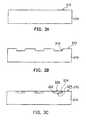
- FIG. 3A to 3Care schematic diagrams showing the sectional view of the structure of the third embodiment of the present invention.
- FIG. 4A to 4Iare schematic diagrams showing the sectional view of the structure of the forth embodiment of the present invention.
- FIG. 5A to 5Eare schematic diagrams showing the sectional view of the structure of the fifth embodiment of the present invention.
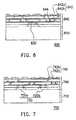
- FIG. 6is a schematic diagram showing the section view of the chip package structure of a preferred embodiment of the present invention with one die.
- FIG. 7is a schematic diagram showing the section view of the chip package structure of a preferred embodiment of the present invention with a plurality of dies.
- FIG. 8is a magnified diagram showing the sectional view of the chip package structure of a preferred embodiment of the present invention.
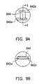
- FIG. 9A , 9 Bare schematic diagrams of the top and side view respectively of the patterned wiring layer of the thin-film circuit layer with a passive device.
- FIG. 10Ais a schematic diagram of the formation of a passive device by a single layer of patterned wiring layer of the thin-film circuit layer.
- FIG. 10Bis a schematic diagram of the formation of a passive device by a double layer of patterned wiring layer of the thin-film circuit layer.
- FIG. 11Ais a schematic diagram of the formation of a passive device by a single layer of patterned wiring layer of the thin-film circuit layer.
- FIG. 11Bis a schematic diagram of the formation of a passive device by a double layer of patterned wiring layer of the thin-film circuit layer.
- FIG. 11Cis a schematic diagram of the formation of a passive device by a double layer of patterned wiring layer of the thin-film circuit layer.
- an organic substrate 110 with a surface 112is provided.
- the material of the organic substratecomprises polymer resin, epoxy resin, imide resin, or the like, plastic, or thermosetting plastic.
- the fabrication of the organic substratescan be accomplished by existing printed circuit board (PCB) fabrication technique.
- the methodincludes heat pressing a plurality of insulating core boards or injection molding to form organic substrate 110 .
- a plurality of dies 120 having an active surface 122 and a corresponding backside 124is provided, where the active devices are formed on active surface 122 of dies 120 . Furthermore, dies 120 have a plurality of metal pads 126 located on active surface 122 of dies 120 acting as the output terminal of dies 120 to transmit signals to the external circuitry. Backside 124 of dies 120 is adhered to surface 112 of organic substrate 110 by a conductive paste or adhesive tape. Therefore, active surface 122 of dies 120 is facing upwards along surface 112 of organic substrate 110 .
- a filling layer 130is formed on top of surface 112 of organic substrate 110 surrounding the peripheral of dies 120 to fill the gap between dies 120 .
- the top face of filling layer 130is approximately planar to active surface 122 of dies 120 .
- the material of filling layer 130can be epoxy, polymer, or the like. After curing of filling layer 130 , a grinding or etching process is applied to planarize filling layer 130 so the top face of filling layer 130 is planar to active surface 122 of dies 120 .
- a dielectric layer 142is formed on top of filling layer 130 and active surface 122 of dies 120 .
- Dielectric layer 142is patterned according to metal pads 126 on dies 120 to form thru-holes 142 a .
- the material of dielectric layer 142can be poly-Imide (PI), benzocyclobutene (BCB), porous dielectric material, stress buffer material, or the like. Patternization of dielectric layer 142 can be performed by photo via, laser ablation, plasma etching, or the like.
- filling layer 130is used to support dielectric layer 142 so dielectric layer 142 can be formed planarized on top of organic substrate 110 and dies 120 without an uneven surface.
- dielectric layer 142also fills the peripheral of dies 120 , meaning the gap between dies 120 . Therefore the bottom structure of dielectric layer 142 can replace the structure of filling layer 130 covering entirely surface 112 of organic substrate 110 and surrounding dies 120 .
- the method of forming dielectric layer 142includes first depositing a layer of dielectric layer 142 entirely over dies 120 and organic substrate 110 , then after curing, grinding or etching process is performed to planarize dielectric layer 142 .
- a patterned wiring layer 144is formed on top of dielectric layer 142 by photolithography and sputtering, electroplating, or electro-less plating. Wherein part of the conductive material from patterned wiring layer 144 will be injected into thru-holes 142 a to form vias 142 b , copper (Cu) is used as the material for patterned wiring layer 144 .
- thru-holes 142 acan be pre-filled with a conductive material such as a conductive glue to form vias 142 b .
- patterned wiring layer 144is electrically connected to metal pads 126 of dies 120 . It is to be noted that part of patterned wiring layer 144 extends to a region outside active surface 122 of dies 120 . Dielectric layer 142 and patterned wiring layer 144 form a thin-film circuit layer 140 .
- dielectric layer 146can be formed similarly to dielectric layer 142 on top of dielectric layer 142 and patterned wiring layer 144 .
- Dielectric layer 146is also patterned to form thru-holes 146 a , whereas thru-holes 146 a correspond to bonding pads 144 a of patterned wiring layer 144 .
- a patterned wiring layer 148can be formed on dielectric layer 146 in a similar way as patterned wiring layer 144 . Wherein part of the conductive material from patterned wiring layer 148 will be injected into each thru-hole 146 a for forming a via 146 b .
- patterned wiring layer 148is electrically connected to patterned wiring layer 144 by vias 146 b , and further electrically connected to metal pads 126 of die 120 by vias 142 b of thru-hole 142 a . Therefore, thin-film circuit layer 140 further comprises dielectric layer 146 , a plurality of vias 146 b , and patterned wiring layer 148 .
- the number of patterned wiring layers ( 144 , 148 . . . ) and dielectric layers ( 142 , 146 . . . ) for electrical insulationmay be increased. All patterned wiring layers ( 144 , 148 . . . ) are electrically connected by vias ( 146 b . . . ) of thru-holes ( 146 a . . . ).
- thin-film circuit layer 140comprises at least one dielectric layer 142 , one patterned wiring layer 144 , and a plurality of vias 142 b .
- patterned wiring layer ( 144 , 148 . . . ) and vias ( 142 b , 146 b ) of thin-film circuit layer 140form an external circuitry of thin-film circuit layer 140 .
- a patterned passivation layer 150is formed on top of dielectric layer 146 and patterned wiring layer 148 .
- Patterned passivation layer 150is used to protect patterned wiring layer 148 and expose the plurality of bonding pads 148 a of patterned wiring layer 148 , whereas some of bonding pads 148 a are in a region outside active surface 122 of dies 120 .
- the redistribution of metal pads 126 on organic substrate 110requires multiple layers of patterned wiring layers ( 144 , 148 . . . ) and a patterned passivation layer 150 formed on the very top, which is furthest away from organic substrate 110 .
- patterned passivation layer 150will be formed directly on patterned wiring layer 144 .
- the material of patterned passivation layer 150can be anti-solder insulating coating or other insulating material.
- a bonding point 160can be placed on bonding pads 148 a serving as an interface for electrically connecting dies 120 to the external circuitry.
- bonding point 160 illustrated in FIG. 1His a ball but it is not limited to any formation, which might include a bump, pin, or the like.
- ball connectormaybe solder ball
- bump connectormaybe solder bump, gold bump, or the like.
- the first embodiment of the present inventionis a chip package structure with an organic substrate and a plurality of dies on the organic substrate.
- the external circuitry of the thin-film circuit layerallows the metal pads of the die to fan out.
- bonding pads corresponding to the metal pads of the diessuch as solders balls, bumps, or pins as the signal input terminals, the distance of the signal path is effectively decreased. As a result, signal delay and attenuation are reduced to increase performance of the die.
- the present inventionuses existing technology on and equipment for fabricating PCB for the fabrication of the organic substrate by heat pressing a plurality of insulating core boards.
- the organic substratecan also be fabricated in large volume by injection molding. As a result of the low fabrication and material cost of the organic substrate, the cost of chip packaging is also lowered.
- the second embodiment of the present inventiondiffers from the first embodiment by having inwardly protruded areas in the organic substrate. This area is for placement of the die with the backside of the die adhered to the bottom of the area so the overall thickness of the chip package structure is reduced.
- FIG. 2A to 2Care schematic diagrams of the sectional view of the second embodiment illustrating the fabrication of the structure.
- an organic substrate 210 with a surface 212is provided.
- a plurality of inwardly protruded areas 214is formed on surface 212 of organic substrate 210 by machining such as milling.
- the depth of each inwardly protruded area 214is approximately equal to the thickness of die 220 , therefore the outline and depth of inwardly protruded areas 214 will be the same as dies 220 in FIG. 2C .
- backside 224 of dies 220is adhered to the bottom of inwardly protruded areas 214 so dies 220 are inlayed in inwardly protruded areas 214 .
- Active surface 222 of dies 220is exposed along surface 212 of organic substrate 210 .
- An alternative method of forming inwardly protruded areas 214 in organic substrate 210 in FIG. 2Bis applying the existing technique is fabricating PCB on two core boards: a first organic layer 210 a and a second organic layer 210 b , as illustrated in FIG. 2D .
- Organic layer 210 ahas openings 214 a and by overlapping the first organic layer 210 a and the second organic layer 210 b and heat pressing them together, openings 214 a in organic layer 210 a will form inwardly protruded areas 214 in organic layer 210 b as seen before in FIG. 2B , as illustrated in FIG. 2E .
- the thickness of organic layer 210 ais approximately equal to that of die 220 so the depth of inwardly protruded areas 214 is approximately equal to the thickness of die 220 .
- the second embodiment of the present inventionis an organic substrate with a plurality of inwardly protruded areas for inlaying dies by adhering the backside of the dies to the bottom of the inwardly protruded areas and exposing the active surface of the dies.
- a thin-film circuit layeris formed on top of the dies and the organic substrate to fan out the metal pads of the dies by using the external circuitry of the thin-film circuit layer. Due to the inlay of the dies in the organic substrate, thinning of the thickness of the chip package structure is effectively achieved and the surface of the organic substrate provides enough planarity and support for the formation of the thin-film circuit layer.
- the third embodiment of the present inventiondiffers from the second embodiment of the present invention by using an integrated organic substrate with at least one organic layer and one heat conducting layer.
- FIG. 3A to 3Care schematic diagrams of the sectional view of the third embodiment illustrating the fabrication of the structure.
- an integrated organic substrate 310consists of an organic layer 310 a with multiple openings 314 a and a heat conducting layer 310 b , wherein the material of heat conducting layer 310 b maybe metal.
- organic layer 310 ais placed overlapping heat conducting layer 31013 so openings 314 a of organic layer 310 a form inwardly protruded areas 314 on heat conducting layer 310 b .
- backside 324 of die 320is adhered to the bottom of inwardly protruded areas 314 so dies 320 are inlayed in organic substrate 310 with active surface 322 of die 320 exposed along surface 312 of organic board 310 .
- FIG. 3Aorganic layer 310 a with openings 314 a is provided, openings 314 a are formed at the same time when organic layer 310 a is formed for example by injection molding.
- FIG. 3Borganic layer 310 a is overlapped on heat conducting layer 310 b so openings 314 a of organic layer 310 a can form inwardly protruded areas 314 on the surface of heat conducting layer 310 b.
- the third embodiment of the present inventionis an integrated organic substrate with an organic layer with a plurality of openings and a heat conducting layer.
- the openings in the organic layerwill form the inwardly protruded areas in the integrated organic substrate.
- the backside of the dieadheres to the bottom of the inwardly protruded areas so the dies are inlayed in the inwardly protruded areas and exposing the active surface of the dies.
- This integrated organic substratecan efficiently dissipate heat from the dies to the outside because the bottom of the inwardly protruded area is the surface of the heat conducting material.
- the surface of the organic substrateprovides enough planarity and support for the formation of the thin-film circuit layer.
- FIG. 4A to 4Eare schematic diagrams of the sectional view of the fourth embodiment illustrating the fabrication of the structure.
- an organic substrate 410 with a first surface 412 and a plurality of dies 420are provided.
- the dies 420have an active surface 422 , a backside 424 , and a plurality of metal pads 426 located on active surface 422 .
- the fourth embodiment of the present inventiondiffers from the third embodiment of the present invention by placing active surface 422 of die 420 downwards facing first surface 412 of organic substrate 410 .
- a filling layer 430is formed on top of first surface 412 of organic substrate 410 after active surface 422 of die 420 is adhered to first surface 412 of organic substrate 410 .
- Filling layer 430covers entirely first surface 412 of organic substrate 410 and surrounds dies 420 .
- the material of filling layer 430maybe an oxide, epoxy, or the like.
- a planarization processsuch as grinding is performed to planarize filling layer 430 and backside 424 of dies 420 .
- the thickness of the active devices and traces (not shown) on active surface 422 of die 420is much less than that of die 420 , the thickness of die 420 should not be too small because cracks or damage to the die will occur during machine handling.
- the present inventiondirectly adheres active surface 422 of dies 420 to first surface 412 of organic substrate 410 without further machine handling.
- a grinding processis performed on backside 424 of dies 420 to reduce the thickness of dies 420 .
- dies 420are ground to a very small thickness allowing the final chip package structure to be much thinner.
- a second organic substrate 440 with a second surface 442is adhered to filling layer 430 and dies 420 creating a sandwich effect with filling layer 430 and dies 420 in between two organic substrates 410 and 440 .
- First organic substrate 410is used to provide a planar surface for dies 420 to adhere to and to serve as an insulating layer. Therefore organic substrate 410 can be replaced by substrate made of glass or other organic material.
- first thru-holes 410 aare formed on first organic substrate 410 for exposing metal pads 426 on active surface 422 of die 420 .
- First thru-holes 410 acan be formed by machine drilling, laser, plasma etching, or similar methods.
- a first patterned wiring layer 450is formed on first organic substrate 410 .
- first vias 410 b in first thru-holes 410 aare formed by either filling first thru-holes 410 a with part of the conductive material from patterned wiring layer 450 or pre-filling first thru-holes 410 a with a conductive material before the formation of patterned wiring layer 450 .
- a part of patterned wiring layer 450will extend to a region outside active surface 422 of die 420 .
- a dielectric layer 462is formed on first organic substrate 410 and first patterned wiring layer 450 .
- dielectric layer 462is patterned to form a plurality of second thru-holes 462 a , which correspond to bonding pad 450 a of patterned wiring layer 450 .
- a second patterned wiring layer 464is formed on top of dielectric layer 462 .
- second vias 462 b in thru-holes 462 acan be formed by either filling second thru-holes 462 a with part of the conductive material from patterned wiring layer or pre-filling second thru-holes 462 a with a conductive material before the formation of patterned wiring layer 464 .
- dielectric layer ( 462 . . . )in order to redistribute metal pads 426 of dies 420 on second organic substrate 440 , dielectric layer ( 462 . . . ), second vias ( 462 a . . . ), and second patterned wiring layer ( 464 . . .
- first organic substrate 410can be repeatedly formed on dies 420 and organic substrate 440 .
- first organic substrate 410first patterned wiring layer 450 , dielectric layer 462 . . . , and second patterned wiring layer 464 . . . form thin-film circuit layer 460 .
- the fourth embodiment of the present inventionis an organic substrate with the active surface of the dies adhered directly to the surface of the first organic substrate.
- a filling layeris formed over the dies and the organic substrate followed by a planarization and thinning process.
- a second organic substrateis adhered to the die and the filling layer.
- a thinning process of the first organic substrateis performed and a plurality of thru-holes filled with conductive material are formed on the first organic substrate.
- a patterned wiring layeris formed on the first organic substrate allowing the external circuitry of the thin-film circuit layer to extend to a region outside the active surface of the die to help fan out the metal pads of the die.
- the advantage of this structureis increased surface stability and accuracy because the active surface of the dies are first adhered to the surface of the first organic substrate.
- the thickness of the diecan be very small for reducing the overall thickness of the chip package because no machine handling of dies is required.
- the fifth embodiment of the present inventiontakes the first half of the fabrication process from the fourth embodiment of the present invention and combines with the second half of the fabrication process from the first embodiment of the present invention.
- FIG. 5A to 5Eare schematic diagrams of the sectional view illustrating the fabrication of the structure.
- an active surface 522 of dies 520is adhered to a first surface 512 of a first organic substrate 510 .
- a filling layer 530is formed on top of dies 520 and first organic substrate 510 covering dies 520 .
- a planarization and thinning process of dies 520 and filling layer 530is performed to planarize backside 524 of dies 520 and filling layer 530 .
- a second organic substrate 540is formed on top of dies 520 and filling layer 530 so backside 524 of dies 520 adheres to second organic substrate 540 .
- First organic substrate 510is used to supply a planarized surface (first surface 512 ), and will be removed in later stages of the fabrication process. Therefore first organic substrate 510 can be replaced by substrates of other materials such as glass, metal, silicon, or other organic material.
- the fifth embodiment of the present inventionis an organic substrate with the active surface of the dies adhered to the surface of the first organic substrate for allowing high surface stability and accuracy. As a result, it eliminates the need of machine handling of the dies to achieve a very small thickness of the die for reducing the overall thickness of the chip package.
- FIG. 6it illustrates the schematic diagram of the sectional view of the chip package structure 600 of the present invention for a single die 620 .
- Die 620is placed on organic substrate 610 , and a thin-film circuit layer 640 is formed on top of die 620 and organic substrate 610 .
- External circuitry 642 of thin-film circuit layer 640has at least has one patterned wiring layer 642 a and a plurality of vias 642 b .
- the thickness of the inner traces inside die 620is usually under 1 micron, but because the high amount of traces collocated together so RC delay is relatively high and the power/ground bus requires a large area. As a result, the area of die 620 is not enough to accommodate the power/ground bus.
- the chip package structure 600uses thin-film circuit layer 640 and external circuitry 642 with wider, thicker, and longer traces to alleviate the problem. These traces act an interface for transmitting signals for the internal circuitry of die 620 or the power/ground bus of die 620 . This will improve the performance of die 620 .
- FIG. 8it illustrates a magnified view of the sectional view of the chip package structure of the present invention.
- Active surface 622 of die 620has a plurality of active devices 628 a , 628 b , and an internal circuitry 624 .
- the internal circuitry 624forms a plurality of metal pads 626 on the surface of die 620 . Therefore signals are transmitted from active devices 628 a to external circuitry 642 via internal circuitry 624 of die 620 , and from external circuitry 642 back to another active device 628 b via internal circuitry 624 .
- the traces of external circuitry 642are wider, longer, and thicker than that of internal circuitry 624 for providing an improved transmission path.
- external circuitry 642further comprises at least one passive device 644 including a capacitor, an inductor, a resistor, a wave-guide, a filter, a micro electronic mechanical sensor (MEMS), or the like.
- Passive device 644can be located on a single layer of patterned wiring layer 642 a or between two layers of patterned wiring layers 642 a .
- passive device 644can be formed by printing or other method on two bonding points on patterned wiring layer 642 a when forming thin-film layer 640 .
- a comb-shape passive device 644(such as a comb capacitor) is formed directly on a single patterned wiring layer.
- FIG. 10Aa comb-shape passive device 644 (such as a comb capacitor) is formed directly on a single patterned wiring layer.
- passive device 644(such as a capacitor) is formed between two layers of patterned wiring layers 642 a with an insulating material 646 in between. Wherein the original dielectric layer (not shown) can replace insulating material 646 .
- passive device 644(such as an inductor) is formed by making a single layer of patterned wiring layer 642 a into a circular or square (not shown) spiral.
- column-shape passive device 644(such as an inductor) is formed by using two layers of patterned wiring layers 642 a and a plurality of vias 642 b to surround an insulating material 646 forming a column.
- FIG. 11Apassive device 644 (such as an inductor) is formed by making a single layer of patterned wiring layer 642 a into a circular or square (not shown) spiral.
- column-shape passive device 644(such as an inductor) is formed by using two layers of patterned wiring layers 642 a and a plurality of vias 642 b
- circular-shaped passive device 644(such as an inductor) is formed by using slanted traces from two layers of patterned wiring layers and a plurality of vias 642 b to surround an insulating material 646 in a circular manner forming a pie.
- the above structuresallow the original externally welded passive devices to be integrated into the inside of the chip package structure.
- FIG. 6illustrates a chip package structure 600 for a single die 620 but FIG. 7 illustrates a chip package structure 700 for a plurality of dies.
- Chip package structure 700 in FIG. 7differs from chip package structure 600 in FIG. 6 by having a die module 720 , which comprises at least one or more dies such as die 720 a , 720 b .
- Die 720 a , 720 bare electrically connected by the external circuitry of the thin-film circuit layer.
- the function of die 720 a , 720 bcan be the same or different and can be integrated together by external circuitry 742 to form a multi-die module (MCM) by packaging same or different dies into one chip package structure.
- MCMmulti-die module
- the present inventionprovides a chip packaging method by adhering a die to an organic substrate or to an inwardly protruded area of an organic substrate, and forming a thin-film circuit layer with bonding pads and points above the die and organic substrate.
- This structurecan fan out the metal pads on the die to achieve a thin chip package structure with high pin count.
- the chip package of the present inventionis performed directly on the die and the organic substrate for fanning out the metal pads on the die. It does not require flip chip or wire bonding to connect the die to the micro-spaced contact points of a package substrate or carrier.
- the present inventioncan reduce cost because the package substrate with micro-spaced contacts is very expensive.
- the signal transmission path of the present inventionis reduced to lessen the effect of signal delay and attenuation, which improves the performance of the die.
- FIG. 6illustrates a chip package structure 600 for a single die 620 but FIG. 7 illustrates a chip package structure 700 for a plurality of dies.
- Chip package structure 700 in FIG. 7differs from chip package structure 600 in FIG. 6 by having a die module 720 , which comprises at least one or more dies such as die 720 a , 720 b mounted on an organic substrate 710 .
- External circuity 742 of thin-film circuit layer 740has at least has one patterned wiring layer 742 a and a plurality of vias 742 b .
- Die 720 a , 720 bare electrically connected by the external circuitry 742 of the thin-film circuit layer 740 .
- die 720 a , 720 bcan be the same or different and can be integrated together by external circuitry 742 to fonn a multi-die module (MCM) by packaging same or different dies into one chip package structure. When multiple dies are packaged into the same chip package structure, singulation process is performed on the determined number of dies.
- MCMmulti-die module
- the third embodiment of the present inventionprovides an integrated substrate comprises an organic layer and a heat conducting layer.
- a plurality of openingscan be pre-formed on the organic layer so inwardly protruded areas are formed for inlaying the die when the organic layer overlaps the heat conducting layer.
- the heat conducting layerhelps to dissipate heat to the outside from the die during operation, which will effectively increase performance.
- the thin-film layer circuit of the present inventionis used to transmit signals between two main active devices inside the die, used as a power/ground bus, or used to add in passive devices. Furthermore, the chip package structure of the present invention can accommodate one or more dies with similar or different functions.
- the external circuitry of the thin-film circuit layerelectrically connects the multiple dies together and can be used in a MCM package.
- the chip package structure of the present inventionadapts the MCM, the external circuitry of the thin-film circuit layer, the passive devices of the external circuitry to form a package that is called “system in package”.
Landscapes
- Engineering & Computer Science (AREA)
- Computer Hardware Design (AREA)
- Power Engineering (AREA)
- Microelectronics & Electronic Packaging (AREA)
- General Physics & Mathematics (AREA)
- Physics & Mathematics (AREA)
- Condensed Matter Physics & Semiconductors (AREA)
- Manufacturing & Machinery (AREA)
- Ceramic Engineering (AREA)
- Semiconductor Integrated Circuits (AREA)
- Internal Circuitry In Semiconductor Integrated Circuit Devices (AREA)
- Structures For Mounting Electric Components On Printed Circuit Boards (AREA)
- Wire Bonding (AREA)
Abstract
Description
Claims (32)
Priority Applications (1)
| Application Number | Priority Date | Filing Date | Title |
|---|---|---|---|
| US13/031,163US8471361B2 (en) | 2001-12-31 | 2011-02-18 | Integrated chip package structure using organic substrate and method of manufacturing the same |
Applications Claiming Priority (6)
| Application Number | Priority Date | Filing Date | Title |
|---|---|---|---|
| TW90133093A | 2001-12-31 | ||
| TW090133093ATW544882B (en) | 2001-12-31 | 2001-12-31 | Chip package structure and process thereof |
| TW90133093 | 2001-12-31 | ||
| US10/055,499US7413929B2 (en) | 2001-12-31 | 2002-01-22 | Integrated chip package structure using organic substrate and method of manufacturing the same |
| US12/172,275US7898058B2 (en) | 2001-12-31 | 2008-07-14 | Integrated chip package structure using organic substrate and method of manufacturing the same |
| US13/031,163US8471361B2 (en) | 2001-12-31 | 2011-02-18 | Integrated chip package structure using organic substrate and method of manufacturing the same |
Related Parent Applications (1)
| Application Number | Title | Priority Date | Filing Date |
|---|---|---|---|
| US12/172,275ContinuationUS7898058B2 (en) | 2001-12-31 | 2008-07-14 | Integrated chip package structure using organic substrate and method of manufacturing the same |
Publications (2)
| Publication Number | Publication Date |
|---|---|
| US20110205720A1 US20110205720A1 (en) | 2011-08-25 |
| US8471361B2true US8471361B2 (en) | 2013-06-25 |
Family
ID=21680114
Family Applications (5)
| Application Number | Title | Priority Date | Filing Date |
|---|---|---|---|
| US10/055,499Expired - LifetimeUS7413929B2 (en) | 2001-12-31 | 2002-01-22 | Integrated chip package structure using organic substrate and method of manufacturing the same |
| US10/728,150Expired - LifetimeUS7345365B2 (en) | 2001-12-31 | 2003-12-03 | Electronic component with die and passive device |
| US10/794,472Expired - LifetimeUS7297614B2 (en) | 2001-12-31 | 2004-03-05 | Method for fabricating circuitry component |
| US12/172,275Expired - Fee RelatedUS7898058B2 (en) | 2001-12-31 | 2008-07-14 | Integrated chip package structure using organic substrate and method of manufacturing the same |
| US13/031,163Expired - Fee RelatedUS8471361B2 (en) | 2001-12-31 | 2011-02-18 | Integrated chip package structure using organic substrate and method of manufacturing the same |
Family Applications Before (4)
| Application Number | Title | Priority Date | Filing Date |
|---|---|---|---|
| US10/055,499Expired - LifetimeUS7413929B2 (en) | 2001-12-31 | 2002-01-22 | Integrated chip package structure using organic substrate and method of manufacturing the same |
| US10/728,150Expired - LifetimeUS7345365B2 (en) | 2001-12-31 | 2003-12-03 | Electronic component with die and passive device |
| US10/794,472Expired - LifetimeUS7297614B2 (en) | 2001-12-31 | 2004-03-05 | Method for fabricating circuitry component |
| US12/172,275Expired - Fee RelatedUS7898058B2 (en) | 2001-12-31 | 2008-07-14 | Integrated chip package structure using organic substrate and method of manufacturing the same |
Country Status (2)
| Country | Link |
|---|---|
| US (5) | US7413929B2 (en) |
| TW (1) | TW544882B (en) |
Cited By (4)
| Publication number | Priority date | Publication date | Assignee | Title |
|---|---|---|---|---|
| US8835221B2 (en) | 2001-12-31 | 2014-09-16 | Qualcomm Incorporated | Integrated chip package structure using ceramic substrate and method of manufacturing the same |
| US9184104B1 (en) | 2014-05-28 | 2015-11-10 | Stats Chippac, Ltd. | Semiconductor device and method of forming adhesive layer over insulating layer for bonding carrier to mixed surfaces of semiconductor die and encapsulant |
| US20170278836A1 (en)* | 2012-08-02 | 2017-09-28 | Infineon Technologies Ag | Integrated System and Method of Making the Integrated System |
| RU2655678C1 (en)* | 2014-09-18 | 2018-05-29 | Интел Корпорейшн | Method of building wlcsp components in e-wlb and e-plb |
Families Citing this family (98)
| Publication number | Priority date | Publication date | Assignee | Title |
|---|---|---|---|---|
| US7271489B2 (en)* | 2003-10-15 | 2007-09-18 | Megica Corporation | Post passivation interconnection schemes on top of the IC chips |
| US6673698B1 (en) | 2002-01-19 | 2004-01-06 | Megic Corporation | Thin film semiconductor package utilizing a glass substrate with composite polymer/metal interconnect layers |
| TW517361B (en) | 2001-12-31 | 2003-01-11 | Megic Corp | Chip package structure and its manufacture process |
| TW503496B (en) | 2001-12-31 | 2002-09-21 | Megic Corp | Chip packaging structure and manufacturing process of the same |
| TW544882B (en) | 2001-12-31 | 2003-08-01 | Megic Corp | Chip package structure and process thereof |
| US7037805B2 (en)* | 2003-05-07 | 2006-05-02 | Honeywell International Inc. | Methods and apparatus for attaching a die to a substrate |
| US6927098B2 (en)* | 2003-05-07 | 2005-08-09 | Honeywell International Inc. | Methods and apparatus for attaching MEMS devices to housing |
| DE10355925B4 (en)* | 2003-11-29 | 2006-07-06 | Semikron Elektronik Gmbh & Co. Kg | Power semiconductor module and method of its manufacture |
| US7459781B2 (en)* | 2003-12-03 | 2008-12-02 | Wen-Kun Yang | Fan out type wafer level package structure and method of the same |
| US7514767B2 (en)* | 2003-12-03 | 2009-04-07 | Advanced Chip Engineering Technology Inc. | Fan out type wafer level package structure and method of the same |
| US7215018B2 (en) | 2004-04-13 | 2007-05-08 | Vertical Circuits, Inc. | Stacked die BGA or LGA component assembly |
| US7262121B2 (en)* | 2004-07-29 | 2007-08-28 | Micron Technology, Inc. | Integrated circuit and methods of redistributing bondpad locations |
| JP4880218B2 (en)* | 2004-12-22 | 2012-02-22 | 三洋電機株式会社 | Circuit equipment |
| EP1762928A1 (en)* | 2005-09-09 | 2007-03-14 | Agilent Technologies, Inc. | Graphics device comprising remote transfer controller for remote visualization |
| US20070114643A1 (en)* | 2005-11-22 | 2007-05-24 | Honeywell International Inc. | Mems flip-chip packaging |
| US7491567B2 (en)* | 2005-11-22 | 2009-02-17 | Honeywell International Inc. | MEMS device packaging methods |
| TW200727370A (en)* | 2006-01-12 | 2007-07-16 | Touch Micro System Tech | Integrated die packaging structure and manufacturing process thereof |
| CN100392852C (en)* | 2006-04-12 | 2008-06-04 | 江苏长电科技股份有限公司 | Flat bump type ultra-thin packaging substrate for electronic components and manufacturing method thereof |
| CN100392851C (en)* | 2006-04-12 | 2008-06-04 | 江苏长电科技股份有限公司 | Planar bump type ultra-thin packaging substrate for semiconductor components and manufacturing method thereof |
| DE102006019244B4 (en)* | 2006-04-21 | 2008-07-03 | Infineon Technologies Ag | Benefit and semiconductor device made of a composite board with semiconductor chips and plastic housing composition and method for producing the same |
| US7830004B2 (en)* | 2006-10-27 | 2010-11-09 | Taiwan Semiconductor Manufacturing Company, Ltd. | Packaging with base layers comprising alloy 42 |
| US7791199B2 (en) | 2006-11-22 | 2010-09-07 | Tessera, Inc. | Packaged semiconductor chips |
| US8569876B2 (en) | 2006-11-22 | 2013-10-29 | Tessera, Inc. | Packaged semiconductor chips with array |
| US20080122074A1 (en)* | 2006-11-28 | 2008-05-29 | Silicon Storage Tech., Inc. | Multi-chip electronic circuit module and a method of manufacturing |
| US7608538B2 (en)* | 2007-01-05 | 2009-10-27 | International Business Machines Corporation | Formation of vertical devices by electroplating |
| TWI340445B (en)* | 2007-01-10 | 2011-04-11 | Advanced Semiconductor Eng | Manufacturing method for integrating passive component within substrate |
| US8405196B2 (en) | 2007-03-05 | 2013-03-26 | DigitalOptics Corporation Europe Limited | Chips having rear contacts connected by through vias to front contacts |
| US7964961B2 (en)* | 2007-04-12 | 2011-06-21 | Megica Corporation | Chip package |
| US7687318B2 (en) | 2007-05-04 | 2010-03-30 | Stats Chippac, Ltd. | Extended redistribution layers bumped wafer |
| US8723332B2 (en)* | 2007-06-11 | 2014-05-13 | Invensas Corporation | Electrically interconnected stacked die assemblies |
| WO2008157722A1 (en)* | 2007-06-19 | 2008-12-24 | Vertical Circuits, Inc. | Wafer level surface passivation of stackable integrated circuit chips |
| TW200917391A (en)* | 2007-06-20 | 2009-04-16 | Vertical Circuits Inc | Three-dimensional circuitry formed on integrated circuit device using two-dimensional fabrication |
| US7868445B2 (en)* | 2007-06-25 | 2011-01-11 | Epic Technologies, Inc. | Integrated structures and methods of fabrication thereof with fan-out metallization on a chips-first chip layer |
| US7605092B2 (en) | 2007-06-29 | 2009-10-20 | Silicon Storage Technology, Inc. | Passive elements, articles, packages, semiconductor composites, and methods of manufacturing same |
| KR20090007120A (en)* | 2007-07-13 | 2009-01-16 | 삼성전자주식회사 | Wafer level laminated package to achieve redistribution through encapsulation and manufacturing method |
| US8217511B2 (en)* | 2007-07-31 | 2012-07-10 | Freescale Semiconductor, Inc. | Redistributed chip packaging with thermal contact to device backside |
| WO2009017835A2 (en)* | 2007-07-31 | 2009-02-05 | Tessera, Inc. | Semiconductor packaging process using through silicon vias |
| WO2009020467A1 (en)* | 2007-08-07 | 2009-02-12 | Skyworks Solutions, Inc. | Near chip scale package integration process |
| US7595226B2 (en)* | 2007-08-29 | 2009-09-29 | Freescale Semiconductor, Inc. | Method of packaging an integrated circuit die |
| WO2009035849A2 (en) | 2007-09-10 | 2009-03-19 | Vertical Circuits, Inc. | Semiconductor die mount by conformal die coating |
| US20090085187A1 (en)* | 2007-09-28 | 2009-04-02 | Ward Scott | Loading mechanism for bare die packages and lga socket |
| WO2009052150A1 (en)* | 2007-10-18 | 2009-04-23 | Vertical Circuits, Inc. | Chip scale stacked die package |
| KR101375660B1 (en)* | 2008-02-22 | 2014-03-19 | 삼성전자주식회사 | A resonator, bandpass filter and manufacturing method of resonator using overlay electromagnetic bandgap structure |
| US20090212381A1 (en)* | 2008-02-26 | 2009-08-27 | Tessera, Inc. | Wafer level packages for rear-face illuminated solid state image sensors |
| US20100053407A1 (en)* | 2008-02-26 | 2010-03-04 | Tessera, Inc. | Wafer level compliant packages for rear-face illuminated solid state image sensors |
| CN101999167B (en)* | 2008-03-12 | 2013-07-17 | 伊文萨思公司 | Support mounted electrically interconnected die assembly |
| US7863159B2 (en)* | 2008-06-19 | 2011-01-04 | Vertical Circuits, Inc. | Semiconductor die separation method |
| US9153517B2 (en) | 2008-05-20 | 2015-10-06 | Invensas Corporation | Electrical connector between die pad and z-interconnect for stacked die assemblies |
| WO2009145727A1 (en)* | 2008-05-28 | 2009-12-03 | Agency For Science, Technology And Research | A semiconductor structure and a method of manufacturing a semiconductor structure |
| TWI387074B (en)* | 2008-06-05 | 2013-02-21 | Chipmos Technologies Inc | Grain stack structure and forming method thereof |
| TWI387014B (en)* | 2008-06-05 | 2013-02-21 | Chipmos Technologies Inc | Die reconfiguration structure with sacrificial substrate and packaging method thereof |
| US8114708B2 (en)* | 2008-09-30 | 2012-02-14 | General Electric Company | System and method for pre-patterned embedded chip build-up |
| JP5161732B2 (en)* | 2008-11-11 | 2013-03-13 | 新光電気工業株式会社 | Manufacturing method of semiconductor device |
| WO2010151578A2 (en)* | 2009-06-26 | 2010-12-29 | Vertical Circuits, Inc. | Electrical interconnect for die stacked in zig-zag configuration |
| DE102009029201B4 (en) | 2009-09-04 | 2019-05-09 | Robert Bosch Gmbh | Method for producing a component comprising a microstructured or nanostructured component |
| EP2309829A1 (en)* | 2009-09-24 | 2011-04-13 | Harman Becker Automotive Systems GmbH | Multilayer circuit board |
| WO2011056668A2 (en) | 2009-10-27 | 2011-05-12 | Vertical Circuits, Inc. | Selective die electrical insulation additive process |
| TWI544604B (en) | 2009-11-04 | 2016-08-01 | 英維瑟斯公司 | Stacked die assembly having reduced stress electrical interconnects |
| US7927919B1 (en)* | 2009-12-03 | 2011-04-19 | Powertech Technology Inc. | Semiconductor packaging method to save interposer |
| US9691734B1 (en)* | 2009-12-07 | 2017-06-27 | Amkor Technology, Inc. | Method of forming a plurality of electronic component packages |
| US8169065B2 (en)* | 2009-12-22 | 2012-05-01 | Epic Technologies, Inc. | Stackable circuit structures and methods of fabrication thereof |
| US20110215465A1 (en)* | 2010-03-03 | 2011-09-08 | Xilinx, Inc. | Multi-chip integrated circuit |
| CN102254834B (en)* | 2010-05-18 | 2016-04-27 | 异基因开发有限责任公司 | Semiconductor package and method |
| US8796135B2 (en)* | 2010-07-23 | 2014-08-05 | Tessera, Inc. | Microelectronic elements with rear contacts connected with via first or via middle structures |
| US9640437B2 (en) | 2010-07-23 | 2017-05-02 | Tessera, Inc. | Methods of forming semiconductor elements using micro-abrasive particle stream |
| US8791575B2 (en) | 2010-07-23 | 2014-07-29 | Tessera, Inc. | Microelectronic elements having metallic pads overlying vias |
| US8610259B2 (en) | 2010-09-17 | 2013-12-17 | Tessera, Inc. | Multi-function and shielded 3D interconnects |
| US8847380B2 (en) | 2010-09-17 | 2014-09-30 | Tessera, Inc. | Staged via formation from both sides of chip |
| KR101059490B1 (en) | 2010-11-15 | 2011-08-25 | 테세라 리써치 엘엘씨 | Conductive pads constructed by embedded traces |
| US8736066B2 (en) | 2010-12-02 | 2014-05-27 | Tessera, Inc. | Stacked microelectronic assemby with TSVS formed in stages and carrier above chip |
| US8637968B2 (en) | 2010-12-02 | 2014-01-28 | Tessera, Inc. | Stacked microelectronic assembly having interposer connecting active chips |
| US8587126B2 (en) | 2010-12-02 | 2013-11-19 | Tessera, Inc. | Stacked microelectronic assembly with TSVs formed in stages with plural active chips |
| US8610264B2 (en) | 2010-12-08 | 2013-12-17 | Tessera, Inc. | Compliant interconnects in wafers |
| US20130115754A1 (en)* | 2011-11-07 | 2013-05-09 | Jing Chen | Micro machining method for a substrate on an underlay |
| US8710658B2 (en) | 2011-11-18 | 2014-04-29 | Cambridge Silicon Radio Limited | Under bump passive components in wafer level packaging |
| US9502270B2 (en) | 2014-07-08 | 2016-11-22 | Taiwan Semiconductor Manufacturing Company, Ltd. | Semiconductor device packages, packaging methods, and packaged semiconductor devices |
| KR101602063B1 (en)* | 2014-10-17 | 2016-03-09 | 목포해양대학교 산학협력단 | 3-dimension printing apparatus and method for packaging a chip using the same |
| US9449919B2 (en)* | 2015-02-12 | 2016-09-20 | Taiwan Semiconductor Manufacturing Company, Ltd. | Semiconductor device, layout design and method for manufacturing a semiconductor device |
| US9666514B2 (en)* | 2015-04-14 | 2017-05-30 | Invensas Corporation | High performance compliant substrate |
| US10869393B2 (en) | 2015-06-29 | 2020-12-15 | Microsoft Technology Licensing, Llc | Pedestal mounting of sensor system |
| US10187977B2 (en) | 2015-06-29 | 2019-01-22 | Microsoft Technology Licensing, Llc | Head mounted computing device, adhesive joint system and method |
| US9871019B2 (en) | 2015-07-17 | 2018-01-16 | Invensas Corporation | Flipped die stack assemblies with leadframe interconnects |
| US9825002B2 (en) | 2015-07-17 | 2017-11-21 | Invensas Corporation | Flipped die stack |
| US9490195B1 (en) | 2015-07-17 | 2016-11-08 | Invensas Corporation | Wafer-level flipped die stacks with leadframes or metal foil interconnects |
| US9508691B1 (en) | 2015-12-16 | 2016-11-29 | Invensas Corporation | Flipped die stacks with multiple rows of leadframe interconnects |
| US10969574B2 (en) | 2016-04-01 | 2021-04-06 | Intel Corporation | Process for creating piezo-electric mirrors in package |
| US10566310B2 (en) | 2016-04-11 | 2020-02-18 | Invensas Corporation | Microelectronic packages having stacked die and wire bond interconnects |
| US9595511B1 (en) | 2016-05-12 | 2017-03-14 | Invensas Corporation | Microelectronic packages and assemblies with improved flyby signaling operation |
| US9728524B1 (en) | 2016-06-30 | 2017-08-08 | Invensas Corporation | Enhanced density assembly having microelectronic packages mounted at substantial angle to board |
| US12068246B2 (en) | 2017-11-30 | 2024-08-20 | Taiwan Semiconductor Manufacturing Company, Ltd. | Redistribution layer layouts on integrated circuits and methods for manufacturing the same |
| US11791299B2 (en) | 2017-11-30 | 2023-10-17 | Taiwan Semiconductor Manufacturing Co., Ltd. | Redistribution layer (RDL) layouts for integrated circuits |
| TWI651022B (en)* | 2017-10-13 | 2019-02-11 | 欣興電子股份有限公司 | Multi-layer circuit structure and manufacturing method thereof |
| CN109673099B (en)* | 2017-10-13 | 2020-09-01 | 欣兴电子股份有限公司 | Multilayer circuit structure and manufacturing method thereof |
| KR102734293B1 (en)* | 2018-12-10 | 2024-11-26 | 삼성전자주식회사 | Method and apparatus for preprocessing fingerprint image |
| US11158580B2 (en)* | 2019-10-18 | 2021-10-26 | Taiwan Semiconductor Manufacturing Co., Ltd. | Semiconductor devices with backside power distribution network and frontside through silicon via |
| WO2023035289A1 (en)* | 2021-09-13 | 2023-03-16 | 上海仁芯生物科技有限公司 | Microfluidic chip having flat dielectric layer surface, preparation method therefor, and manufacturing mold |
| CN114334679B (en)* | 2021-11-11 | 2025-05-27 | 四川航天电子设备研究所 | A packaging method for heterogeneous coplanar integrated chip |
| US20250233036A1 (en)* | 2024-01-15 | 2025-07-17 | Texas Instruments Incorporated | Integrated circuit with a protective layer |
Citations (377)
| Publication number | Priority date | Publication date | Assignee | Title |
|---|---|---|---|---|
| US2920232A (en) | 1958-08-18 | 1960-01-05 | Gen Electric | Display device with storage |
| US3504214A (en) | 1967-01-13 | 1970-03-31 | Westinghouse Canada Ltd | Electroluminescent display device |
| US3634714A (en) | 1970-02-16 | 1972-01-11 | G T Schijeldahl Co | Electroluminescent display device with apertured electrodes |
| US3677112A (en) | 1970-06-08 | 1972-07-18 | John W Keniston | Pincers |
| US3903590A (en) | 1973-03-10 | 1975-09-09 | Tokyo Shibaura Electric Co | Multiple chip integrated circuits and method of manufacturing the same |
| US4021838A (en) | 1974-11-20 | 1977-05-03 | International Business Machines Corporation | Semiconductor integrated circuit devices |
| US4235498A (en) | 1979-07-26 | 1980-11-25 | The Bendix Corporation | Electrical connector with locking means |
| US4402888A (en) | 1981-09-14 | 1983-09-06 | Pamarco Incorporated | Corona discharge treatment roll |
| US4622058A (en) | 1984-06-22 | 1986-11-11 | International Business Machines Corporation | Formation of a multi-layer glass-metallized structure formed on and interconnected to multi-layered-metallized ceramic substrate |
| US4685998A (en) | 1984-03-22 | 1987-08-11 | Thomson Components - Mostek Corp. | Process of forming integrated circuits with contact pads in a standard array |
| US4789647A (en) | 1986-01-08 | 1988-12-06 | U.S. Philips Corporation | Method of manufacturing a semiconductor device, in which a metallization with a thick connection electrode is provided on a semiconductor body |
| US4840923A (en) | 1986-04-30 | 1989-06-20 | International Business Machine Corporation | Simultaneous multiple level interconnection process |
| US4866501A (en) | 1985-12-16 | 1989-09-12 | American Telephone And Telegraph Company At&T Bell Laboratories | Wafer scale integration |
| US4918811A (en) | 1986-09-26 | 1990-04-24 | General Electric Company | Multichip integrated circuit packaging method |
| US5048179A (en) | 1986-05-23 | 1991-09-17 | Ricoh Company, Ltd. | IC chip mounting method |
| US5049980A (en) | 1987-04-15 | 1991-09-17 | Kabushiki Kaisha Toshiba | Electronic circuit device and method of manufacturing same |
| US5055321A (en) | 1988-04-28 | 1991-10-08 | Ibiden Co., Ltd. | Adhesive for electroless plating, printed circuit boards and method of producing the same |
| US5063177A (en) | 1990-10-04 | 1991-11-05 | Comsat | Method of packaging microwave semiconductor components and integrated circuits |
| US5073814A (en) | 1990-07-02 | 1991-12-17 | General Electric Company | Multi-sublayer dielectric layers |
| US5081563A (en) | 1990-04-27 | 1992-01-14 | International Business Machines Corporation | Multi-layer package incorporating a recessed cavity for a semiconductor chip |
| US5083187A (en) | 1990-05-16 | 1992-01-21 | Texas Instruments Incorporated | Integrated circuit device having bumped power supply buses over active surface areas and method of manufacture thereof |
| US5095402A (en) | 1990-10-02 | 1992-03-10 | Rogers Corporation | Internally decoupled integrated circuit package |
| US5099306A (en) | 1988-11-21 | 1992-03-24 | Honeywell Inc. | Stacked tab leadframe assembly |
| US5111278A (en) | 1991-03-27 | 1992-05-05 | Eichelberger Charles W | Three-dimensional multichip module systems |
| US5149662A (en) | 1991-03-27 | 1992-09-22 | Integrated System Assemblies Corporation | Methods for testing and burn-in of integrated circuit chips |
| US5161093A (en) | 1990-07-02 | 1992-11-03 | General Electric Company | Multiple lamination high density interconnect process and structure employing a variable crosslinking adhesive |
| US5188984A (en) | 1987-04-21 | 1993-02-23 | Sumitomo Electric Industries, Ltd. | Semiconductor device and production method thereof |
| US5196377A (en) | 1990-12-20 | 1993-03-23 | Cray Research, Inc. | Method of fabricating silicon-based carriers |
| US5211278A (en) | 1990-01-31 | 1993-05-18 | Lamb-Weston, Inc. | Food transport chain conveyor system |
| US5226232A (en) | 1990-05-18 | 1993-07-13 | Hewlett-Packard Company | Method for forming a conductive pattern on an integrated circuit |
| US5239198A (en) | 1989-09-06 | 1993-08-24 | Motorola, Inc. | Overmolded semiconductor device having solder ball and edge lead connective structure |
| US5241456A (en) | 1990-07-02 | 1993-08-31 | General Electric Company | Compact high density interconnect structure |
| US5250843A (en) | 1991-03-27 | 1993-10-05 | Integrated System Assemblies Corp. | Multichip integrated circuit modules |
| US5281151A (en) | 1991-07-05 | 1994-01-25 | Hitachi, Ltd. | Semiconductor chip carrier, module having same chip carrier mounted therein, and electronic device incorporating same module |
| US5291066A (en) | 1991-11-14 | 1994-03-01 | General Electric Company | Moisture-proof electrical circuit high density interconnect module and method for making same |
| US5300812A (en) | 1992-12-09 | 1994-04-05 | General Electric Company | Plasticized polyetherimide adhesive composition and usage |
| US5324687A (en) | 1992-10-16 | 1994-06-28 | General Electric Company | Method for thinning of integrated circuit chips for lightweight packaged electronic systems |
| US5331204A (en) | 1991-10-17 | 1994-07-19 | Ngk Spark Plug Co., Ltd. | Integrated circuit package in which impendance between signal pads and signal lines is matched by reducing the size of a ground plane |
| US5334874A (en) | 1991-09-13 | 1994-08-02 | Metzler Richard A | Electronic device package |
| US5336928A (en) | 1992-09-18 | 1994-08-09 | General Electric Company | Hermetically sealed packaged electronic system |
| US5353195A (en) | 1993-07-09 | 1994-10-04 | General Electric Company | Integral power and ground structure for multi-chip modules |
| US5353498A (en) | 1993-02-08 | 1994-10-11 | General Electric Company | Method for fabricating an integrated circuit module |
| US5359496A (en) | 1989-12-21 | 1994-10-25 | General Electric Company | Hermetic high density interconnected electronic system |
| US5365790A (en) | 1992-04-02 | 1994-11-22 | Motorola, Inc. | Device with bonded conductive and insulating substrates and method therefore |
| US5366906A (en) | 1992-10-16 | 1994-11-22 | Martin Marietta Corporation | Wafer level integration and testing |
| US5370766A (en) | 1993-08-16 | 1994-12-06 | California Micro Devices | Methods for fabrication of thin film inductors, inductor networks and integration with other passive and active devices |
| US5372967A (en) | 1992-01-27 | 1994-12-13 | Motorola, Inc. | Method for fabricating a vertical trench inductor |
| US5384488A (en) | 1992-06-15 | 1995-01-24 | Texas Instruments Incorporated | Configuration and method for positioning semiconductor device bond pads using additional process layers |
| US5388328A (en) | 1990-03-19 | 1995-02-14 | Hitachi, Ltd. | Process for fabricating an interconnected multilayer board |
| TW241438B (en) | 1993-06-25 | 1995-02-21 | Fuji Electric Co Ltd | |
| US5394490A (en) | 1992-08-11 | 1995-02-28 | Hitachi, Ltd. | Semiconductor device having an optical waveguide interposed in the space between electrode members |
| US5401687A (en) | 1993-04-15 | 1995-03-28 | Martin Marietta Corporation | Process for high density interconnection of substrates and integrated circuit chips containing sensitive structures |
| US5416356A (en) | 1993-09-03 | 1995-05-16 | Motorola, Inc. | Integrated circuit having passive circuit elements |
| US5422513A (en) | 1992-10-16 | 1995-06-06 | Martin Marietta Corporation | Integrated circuit chip placement in a high density interconnect structure |
| US5432675A (en) | 1993-11-15 | 1995-07-11 | Fujitsu Limited | Multi-chip module having thermal contacts |
| US5432677A (en) | 1993-02-09 | 1995-07-11 | Texas Instruments Incorporated | Multi-chip integrated circuit module |
| US5434751A (en) | 1994-04-11 | 1995-07-18 | Martin Marietta Corporation | Reworkable high density interconnect structure incorporating a release layer |
| US5450101A (en) | 1993-07-22 | 1995-09-12 | Seiko Instruments Inc. | Thermal head for a printer |
| US5478773A (en) | 1994-04-28 | 1995-12-26 | Motorola, Inc. | Method of making an electronic device having an integrated inductor |
| US5483421A (en) | 1992-03-09 | 1996-01-09 | International Business Machines Corporation | IC chip attachment |
| US5524339A (en) | 1994-09-19 | 1996-06-11 | Martin Marietta Corporation | Method for protecting gallium arsenide mmic air bridge structures |
| US5532512A (en) | 1994-10-03 | 1996-07-02 | General Electric Company | Direct stacked and flip chip power semiconductor device structures |
| US5541442A (en) | 1994-08-31 | 1996-07-30 | International Business Machines Corporation | Integrated compact capacitor-resistor/inductor configuration |
| US5548099A (en) | 1994-09-13 | 1996-08-20 | Martin Marietta Corporation | Method for making an electronics module having air bridge protection without large area ablation |
| US5548091A (en) | 1993-10-26 | 1996-08-20 | Tessera, Inc. | Semiconductor chip connection components with adhesives and methods for bonding to the chip |
| US5565706A (en) | 1994-03-18 | 1996-10-15 | Hitachi, Ltd. | LSI package board |
| US5566441A (en) | 1993-03-11 | 1996-10-22 | British Technology Group Limited | Attaching an electronic circuit to a substrate |
| US5576517A (en) | 1994-05-23 | 1996-11-19 | General Electric Company | Low Dielectric constant materials for high speed electronics |
| US5583359A (en) | 1995-03-03 | 1996-12-10 | Northern Telecom Limited | Capacitor structure for an integrated circuit |
| US5602059A (en) | 1994-09-08 | 1997-02-11 | Shinko Electric Industries Co., Ltd. | Semiconductor device and method for manufacturing same |
| US5606198A (en) | 1993-10-13 | 1997-02-25 | Yamaha Corporation | Semiconductor chip with electrodes on side surface |
| US5611884A (en) | 1995-12-11 | 1997-03-18 | Dow Corning Corporation | Flip chip silicone pressure sensitive conductive adhesive |
| US5629240A (en) | 1994-12-09 | 1997-05-13 | Sun Microsystems, Inc. | Method for direct attachment of an on-chip bypass capacitor in an integrated circuit |
| US5635762A (en) | 1993-05-18 | 1997-06-03 | U.S. Philips Corporation | Flip chip semiconductor device with dual purpose metallized ground conductor |
| US5648448A (en) | 1995-06-06 | 1997-07-15 | Hitachi Chemical Company, Ltd. | Method of preparation of polyquinolines |
| US5650662A (en) | 1993-08-17 | 1997-07-22 | Edwards; Steven F. | Direct bonded heat spreader |
| US5659201A (en) | 1995-06-05 | 1997-08-19 | Advanced Micro Devices, Inc. | High conductivity interconnection line |
| US5663106A (en) | 1994-05-19 | 1997-09-02 | Tessera, Inc. | Method of encapsulating die and chip carrier |
| US5665989A (en) | 1995-01-03 | 1997-09-09 | Lsi Logic | Programmable microsystems in silicon |
| US5668399A (en) | 1995-02-08 | 1997-09-16 | International Business Machines Corporation | Semiconductor device with increased on chip decoupling capacitance |
| US5691248A (en) | 1995-07-26 | 1997-11-25 | International Business Machines Corporation | Methods for precise definition of integrated circuit chip edges |
| US5696466A (en) | 1995-12-08 | 1997-12-09 | The Whitaker Corporation | Heterolithic microwave integrated impedance matching circuitry and method of manufacture |
| US5717245A (en) | 1994-03-30 | 1998-02-10 | Plessey Semiconductors Limited | Ball grid array arrangement |
| US5729053A (en) | 1994-07-27 | 1998-03-17 | Texas Instruments Incorporated | Apparatus and method for flat circuit assembly |
| US5745984A (en) | 1995-07-10 | 1998-05-05 | Martin Marietta Corporation | Method for making an electronic module |
| US5757079A (en) | 1995-12-21 | 1998-05-26 | International Business Machines Corporation | Method for repairing defective electrical connections on multi-layer thin film (MLTF) electronic packages and the resulting MLTF structure |
| US5757072A (en) | 1994-12-19 | 1998-05-26 | Martin Marietta Corporation | Structure for protecting air bridges on semiconductor chips from damage |
| US5763108A (en) | 1997-03-05 | 1998-06-09 | Headway Technologies, Inc. | High saturtion magnetization material and magnetic head fabricated therefrom |
| US5767564A (en) | 1993-10-19 | 1998-06-16 | Kyocera Corporation | Semiconductor device with a decoupling capacitor mounted thereon having a thermal expansion coefficient matched to the device |
| US5776796A (en) | 1994-05-19 | 1998-07-07 | Tessera, Inc. | Method of encapsulating a semiconductor package |
| US5786239A (en) | 1995-09-20 | 1998-07-28 | Sony Corporation | Method of manufacturing a semiconductor package |
| US5789303A (en) | 1994-11-28 | 1998-08-04 | Northern Telecom Limited | Method of adding on chip capacitors to an integrated circuit |
| US5792594A (en) | 1996-04-01 | 1998-08-11 | Motorola, Inc. | Metallization and termination process for an integrated circuit chip |
| US5817541A (en) | 1997-03-20 | 1998-10-06 | Raytheon Company | Methods of fabricating an HDMI decal chip scale package |
| US5834844A (en) | 1995-03-24 | 1998-11-10 | Shinko Electric Industries Co., Ltd. | Semiconductor device having an element with circuit pattern thereon |
| US5834339A (en) | 1996-03-07 | 1998-11-10 | Tessera, Inc. | Methods for providing void-free layers for semiconductor assemblies |
| US5834832A (en) | 1994-06-09 | 1998-11-10 | Samsung Electronics Co., Ltd. | Packing structure of semiconductor packages |
| US5841193A (en) | 1996-05-20 | 1998-11-24 | Epic Technologies, Inc. | Single chip modules, repairable multichip modules, and methods of fabrication thereof |
| US5854513A (en) | 1995-07-14 | 1998-12-29 | Lg Electronics Inc. | Semiconductor device having a bump structure and test electrode |
| US5854001A (en) | 1992-01-31 | 1998-12-29 | Abbott Laboratories | Hepatitis C virus fusion proteins |
| US5872489A (en) | 1997-04-28 | 1999-02-16 | Rockwell Science Center, Llc | Integrated tunable inductance network and method |
| US5874770A (en) | 1996-10-10 | 1999-02-23 | General Electric Company | Flexible interconnect film including resistor and capacitor layers |
| US5883435A (en) | 1996-07-25 | 1999-03-16 | International Business Machines Corporation | Personalization structure for semiconductor devices |
| US5892288A (en) | 1997-05-30 | 1999-04-06 | Mitsubishi Denki Kabushiki Kaisha | Semiconductor integrated circuit device |
| US5892273A (en) | 1994-10-03 | 1999-04-06 | Kabushiki Kaisha Toshiba | Semiconductor package integral with semiconductor chip |
| US5919548A (en) | 1996-10-11 | 1999-07-06 | Sandia Corporation | Chemical-mechanical polishing of recessed microelectromechanical devices |
| US5929510A (en) | 1996-10-31 | 1999-07-27 | Sarnoff Corporation | Integrated electronic circuit |
| US5932379A (en) | 1998-02-24 | 1999-08-03 | Lucent Technologies Inc. | Repairing fractured wafers in semiconductor manufacturing |
| US5939214A (en) | 1989-05-31 | 1999-08-17 | Advanced Technology Interconnect, Incorporated | Thermal performance package for integrated circuit chip |
| US5939782A (en) | 1998-03-03 | 1999-08-17 | Sun Microsystems, Inc. | Package construction for integrated circuit chip with bypass capacitor |
| US5945741A (en) | 1995-11-21 | 1999-08-31 | Sony Corporation | Semiconductor chip housing having a reinforcing plate |
| US5952726A (en) | 1996-11-12 | 1999-09-14 | Lsi Logic Corporation | Flip chip bump distribution on die |
| US5959357A (en) | 1998-02-17 | 1999-09-28 | General Electric Company | Fet array for operation at different power levels |
| US5973908A (en) | 1995-12-04 | 1999-10-26 | General Electric Company | Structure for thin film capacitors |
| US5994766A (en) | 1998-09-21 | 1999-11-30 | Vlsi Technology, Inc. | Flip chip circuit arrangement with redistribution layer that minimizes crosstalk |
| US6002592A (en) | 1996-12-09 | 1999-12-14 | Sony Corporation | Electronic device and method for manufacturing electronic device |
| US6004867A (en) | 1996-12-16 | 1999-12-21 | Samsung Electronics Co., Ltd. | Chip-size packages assembled using mass production techniques at the wafer-level |
| US6008102A (en) | 1998-04-09 | 1999-12-28 | Motorola, Inc. | Method of forming a three-dimensional integrated inductor |
| US6008070A (en)* | 1998-05-21 | 1999-12-28 | Micron Technology, Inc. | Wafer level fabrication and assembly of chip scale packages |
| US6011314A (en) | 1999-02-01 | 2000-01-04 | Hewlett-Packard Company | Redistribution layer and under bump material structure for converting periphery conductive pads to an array of solder bumps |
| US6010956A (en) | 1996-02-29 | 2000-01-04 | Tokyo Ohka Kogyo Co., Ltd. | Process for producing multilayer wiring boards |
| JP2000003985A (en) | 1998-06-12 | 2000-01-07 | Mitsui High Tec Inc | Manufacture for semiconductor device |
| US6013948A (en) | 1995-11-27 | 2000-01-11 | Micron Technology, Inc. | Stackable chip scale semiconductor package with mating contacts on opposed surfaces |
| US6018463A (en) | 1997-08-22 | 2000-01-25 | Raytheon Company | Large non-hermetic multichip module package |
| US6020220A (en) | 1996-07-09 | 2000-02-01 | Tessera, Inc. | Compliant semiconductor chip assemblies and methods of making same |
| US6022792A (en) | 1996-03-13 | 2000-02-08 | Seiko Instruments, Inc. | Semiconductor dicing and assembling method |
| US6025995A (en) | 1997-11-05 | 2000-02-15 | Ericsson Inc. | Integrated circuit module and method |
| US6030856A (en) | 1996-06-10 | 2000-02-29 | Tessera, Inc. | Bondable compliant pads for packaging of a semiconductor chip and method therefor |
| US6033939A (en) | 1998-04-21 | 2000-03-07 | International Business Machines Corporation | Method for providing electrically fusible links in copper interconnection |
| TW385509B (en) | 1997-02-10 | 2000-03-21 | Matsushita Electronics Corp | Resin sealed semiconductor device and method for manufacturing the same |
| US6043109A (en) | 1999-02-09 | 2000-03-28 | United Microelectronics Corp. | Method of fabricating wafer-level package |
| US6046076A (en) | 1994-12-29 | 2000-04-04 | Tessera, Inc. | Vacuum dispense method for dispensing an encapsulant and machine therefor |
| US6078104A (en) | 1997-02-17 | 2000-06-20 | Seiko Epson Corporation | Carrier film and integrated circuit device using the same and method of making the same |
| US6077726A (en) | 1998-07-30 | 2000-06-20 | Motorola, Inc. | Method and apparatus for stress relief in solder bump formation on a semiconductor device |
| US6080605A (en) | 1998-10-06 | 2000-06-27 | Tessera, Inc. | Methods of encapsulating a semiconductor chip using a settable encapsulant |
| US6087199A (en) | 1998-02-04 | 2000-07-11 | International Business Machines Corporation | Method for fabricating a very dense chip package |
| US6087648A (en) | 1997-07-01 | 2000-07-11 | Semiconductor Energy Laboratory Co., Ltd. | Active matrix display device and method of manufacturing the same |
| US6093584A (en) | 1996-04-18 | 2000-07-25 | Tessera, Inc. | Method for encapsulating a semiconductor package having apertures through a sacrificial layer and contact pads |
| US6104091A (en) | 1996-05-24 | 2000-08-15 | Sony Corporation | Semiconductor package and the manufacturing method |
| US6110806A (en) | 1999-03-26 | 2000-08-29 | International Business Machines Corporation | Process for precision alignment of chips for mounting on a substrate |
| TW403980B (en) | 1999-05-12 | 2000-09-01 | Chipmos Technologies Inc | Wafer level chip scale package structure and the manufacturing method of the same |
| US6121688A (en) | 1996-01-19 | 2000-09-19 | Shinko Electric Industries Co., Ltd. | Anisotropic conductive sheet and printed circuit board |
| US6125039A (en) | 1996-07-31 | 2000-09-26 | Taiyo Yuden Co., Ltd. | Hybrid module |
| US6130116A (en) | 1996-12-13 | 2000-10-10 | Tessera, Inc. | Method of encapsulating a microelectronic assembly utilizing a barrier |
| US6139666A (en) | 1999-05-26 | 2000-10-31 | International Business Machines Corporation | Method for producing ceramic surfaces with easily removable contact sheets |
| US6144100A (en) | 1997-06-05 | 2000-11-07 | Texas Instruments Incorporated | Integrated circuit with bonding layer over active circuitry |
| US6150716A (en) | 1995-01-25 | 2000-11-21 | International Business Machines Corporation | Metal substrate having an IC chip and carrier mounting |
| US6154366A (en) | 1999-11-23 | 2000-11-28 | Intel Corporation | Structures and processes for fabricating moisture resistant chip-on-flex packages |
| US6163456A (en) | 1998-01-30 | 2000-12-19 | Taiyo Yuden, Co., Ltd. | Hybrid module and methods for manufacturing and mounting thereof |
| TW417265B (en) | 1999-02-11 | 2001-01-01 | Hon Hai Prec Ind Co Ltd | Low-cost surface-mount compatible land-grid array (lga) chips cale package (csp) for packaging solder-bumped flip chips |
| US6169319B1 (en) | 1999-08-12 | 2001-01-02 | Tower Semiconductor Ltd. | Backside illuminated image sensor |
| US6175161B1 (en) | 1998-05-22 | 2001-01-16 | Alpine Microsystems, Inc. | System and method for packaging integrated circuits |
| US6177293B1 (en) | 1999-05-20 | 2001-01-23 | Tower Semiconductor Ltd. | Method and structure for minimizing white spots in CMOS image sensors |
| US6180445B1 (en) | 2000-04-24 | 2001-01-30 | Taiwan Semiconductor Manufacturing Company | Method to fabricate high Q inductor by redistribution layer when flip-chip package is employed |
| US6184143B1 (en) | 1997-09-08 | 2001-02-06 | Hitachi, Ltd. | Semiconductor integrated circuit device and fabrication process thereof |
| US6187615B1 (en) | 1998-08-28 | 2001-02-13 | Samsung Electronics Co., Ltd. | Chip scale packages and methods for manufacturing the chip scale packages at wafer level |
| US6187680B1 (en) | 1998-10-07 | 2001-02-13 | International Business Machines Corporation | Method/structure for creating aluminum wirebound pad on copper BEOL |
| TW423127B (en) | 1999-10-15 | 2001-02-21 | Megic Corp | Package structure and method |
| TW423132B (en) | 1999-07-27 | 2001-02-21 | Ind Tech Res Inst | Bumpless flip chip package and method for fabricating |
| US6205032B1 (en) | 1999-03-16 | 2001-03-20 | Cts Corporation | Low temperature co-fired ceramic with improved registration |
| US6221687B1 (en) | 1999-12-23 | 2001-04-24 | Tower Semiconductor Ltd. | Color image sensor with embedded microlens array |
| EP1094511A2 (en) | 1999-10-22 | 2001-04-25 | Lucent Technologies Inc. | Low profile integrated circuit packages |
| US6225692B1 (en) | 1999-06-03 | 2001-05-01 | Cts Corporation | Flip chip package for micromachined semiconductors |
| US6225013B1 (en) | 1999-05-20 | 2001-05-01 | Tower Semiconductor Ltd. | Stitching design rules for forming interconnect layers |
| US6228684B1 (en) | 1998-12-28 | 2001-05-08 | Fujitsu Limited | Wafer-level package, a method of manufacturing thereof and a method of manufacturing semiconductor devices from such a wafer-level package |
| US6228687B1 (en) | 1999-06-28 | 2001-05-08 | Micron Technology, Inc. | Wafer-level package and methods of fabricating |
| US6229203B1 (en) | 1997-03-12 | 2001-05-08 | General Electric Company | Semiconductor interconnect structure for high temperature applications |
| US6232152B1 (en) | 1994-05-19 | 2001-05-15 | Tessera, Inc. | Method of manufacturing a plurality of semiconductor packages and the resulting semiconductor package structures |
| US6236098B1 (en) | 1997-04-16 | 2001-05-22 | Texas Instruments Incorporated | Heat spreader |
| US6235552B1 (en) | 1999-07-09 | 2001-05-22 | Samsung Electronics Co., Ltd. | Chip scale package and method for manufacturing the same using a redistribution substrate |
| US6236101B1 (en) | 1997-11-05 | 2001-05-22 | Texas Instruments Incorporated | Metallization outside protective overcoat for improved capacitors and inductors |
| US6239482B1 (en) | 1999-06-21 | 2001-05-29 | General Electric Company | Integrated circuit package including window frame |
| US6239980B1 (en) | 1998-08-31 | 2001-05-29 | General Electric Company | Multimodule interconnect structure and process |
| US6242282B1 (en) | 1999-10-04 | 2001-06-05 | General Electric Company | Circuit chip package and fabrication method |
| US6242987B1 (en) | 1998-01-08 | 2001-06-05 | Infineon Technologies Ag | Oscillator structure having resonator disposed below oscillator circuit |
| US6245595B1 (en) | 1999-07-22 | 2001-06-12 | National Semiconductor Corporation | Techniques for wafer level molding of underfill encapsulant |
| TW444370B (en) | 2000-05-24 | 2001-07-01 | Siliconware Precision Industries Co Ltd | Flip-chip packaging substrate |
| US6255738B1 (en) | 1996-09-30 | 2001-07-03 | Tessera, Inc. | Encapsulant for microelectronic devices |
| US6271469B1 (en) | 1999-11-12 | 2001-08-07 | Intel Corporation | Direct build-up layer on an encapsulated die package |
| TW449894B (en) | 1999-01-06 | 2001-08-11 | United Microelectronics Corp | Face-to-face multi-chip package |
| US6274391B1 (en) | 1992-10-26 | 2001-08-14 | Texas Instruments Incorporated | HDI land grid array packaged device having electrical and optical interconnects |
| US20010013653A1 (en) | 1998-08-17 | 2001-08-16 | Kazutaka Shoji | Array of electrodes reliable, durable and economical and process for fabrication thereof |
| US6277669B1 (en) | 1999-09-15 | 2001-08-21 | Industrial Technology Research Institute | Wafer level packaging method and packages formed |
| US6278264B1 (en) | 2000-02-04 | 2001-08-21 | Volterra Semiconductor Corporation | Flip-chip switching regulator |
| US6281583B1 (en) | 1999-05-12 | 2001-08-28 | International Business Machines Corporation | Planar integrated circuit interconnect |
| TW452930B (en) | 1998-12-21 | 2001-09-01 | Lin Mou Shiung | Top layers of metal for high performance IC's |
| US6285065B1 (en) | 1999-04-19 | 2001-09-04 | Tower Semiconductor, Ltd. | Color filters formed on integrated circuits |
| TW454318B (en) | 2000-10-19 | 2001-09-11 | Advanced Semiconductor Eng | Chip scale package structure |
| US6287893B1 (en) | 1997-10-20 | 2001-09-11 | Flip Chip Technologies, L.L.C. | Method for forming chip scale package |
| US6288905B1 (en) | 1999-04-15 | 2001-09-11 | Amerasia International Technology Inc. | Contact module, as for a smart card, and method for making same |
| US6288434B1 (en) | 1999-05-14 | 2001-09-11 | Tower Semiconductor, Ltd. | Photodetecting integrated circuits with low cross talk |
| US6288447B1 (en) | 1999-01-22 | 2001-09-11 | Mitsubishi Denki Kabushiki Kaisha | Semiconductor device including a plurality of interconnection layers |
| US6291884B1 (en) | 1999-11-09 | 2001-09-18 | Amkor Technology, Inc. | Chip-size semiconductor packages |
| TW456006B (en) | 2000-07-26 | 2001-09-21 | Advanced Chip Eng Tech Inc | Method of chip scale packaging using chip level packaging technique |
| US6294040B1 (en) | 1996-12-13 | 2001-09-25 | Tessera, Inc. | Transferable resilient element for packaging of a semiconductor chip and method therefor |
| TW457830B (en) | 1999-12-06 | 2001-10-01 | Kanthal Ltd | Electrical resistance ceramic heating element |
| TW457662B (en) | 2000-10-18 | 2001-10-01 | Walsin Advanced Electronics | Fabrication method and structure of a chip size package |
| US20010026010A1 (en) | 2000-03-24 | 2001-10-04 | Michio Horiuchi | Semiconductor device and process of production of same |
| US20010026435A1 (en) | 2000-03-29 | 2001-10-04 | Norio Sakai | Monolithic ceramic electronic component, method for manufacturing same, and electronic device including same |
| US20010028098A1 (en) | 1998-08-07 | 2001-10-11 | Ping Liou | Method and structure of manufacturing a high-q inductor with an air trench |
| US6303423B1 (en) | 1998-12-21 | 2001-10-16 | Megic Corporation | Method for forming high performance system-on-chip using post passivation process |
| US20010031514A1 (en) | 1993-12-17 | 2001-10-18 | Smith John Stephen | Method and apparatus for fabricating self-assembling microstructures |
| US20010033021A1 (en) | 1997-06-06 | 2001-10-25 | Nozomi Shimoishizaka | Semiconductor device and method for manufacturing the same |
| US20010033474A1 (en) | 2000-03-17 | 2001-10-25 | Murata Manufacturing Co., Ltd. | Monolithic ceramic electronic component, method for manufacturing the same, and electronic device |
| US6309915B1 (en) | 1998-02-05 | 2001-10-30 | Tessera, Inc. | Semiconductor chip package with expander ring and method of making same |
| US6313528B1 (en) | 1996-12-13 | 2001-11-06 | Tessera, Inc. | Compliant multichip package |
| US20010037863A1 (en) | 1999-08-06 | 2001-11-08 | Carson Bryan C. | Semiconductor die de-processing using a die holder and chemical mechanical polishing |
| TW463274B (en) | 2000-11-17 | 2001-11-11 | Walsin Advanced Electronics | Manufacturing method for wafer level chip size package |
| US6319827B1 (en) | 1998-06-29 | 2001-11-20 | Inside Technologies | Integrated electronic micromodule and method for making same |
| TW466652B (en) | 2000-01-31 | 2001-12-01 | Wen-Kun Yang | Wafer level package and its process thereof |
| TW466725B (en) | 2001-01-30 | 2001-12-01 | Megic Corp | Multiple chip package |
| US6329224B1 (en) | 1998-04-28 | 2001-12-11 | Tessera, Inc. | Encapsulation of microelectronic assemblies |
| US6329713B1 (en) | 1998-10-21 | 2001-12-11 | International Business Machines Corporation | Integrated circuit chip carrier assembly comprising a stiffener attached to a dielectric substrate |
| US20010051426A1 (en) | 1999-11-22 | 2001-12-13 | Scott K. Pozder | Method for forming a semiconductor device having a mechanically robust pad interface. |
| US6331481B1 (en) | 1999-01-04 | 2001-12-18 | International Business Machines Corporation | Damascene etchback for low ε dielectric |
| TW469549B (en) | 1999-06-29 | 2001-12-21 | Hyundai Electronics Ind | Wafer level stack package and method of fabricating the same |
| US6333557B1 (en) | 2000-09-12 | 2001-12-25 | International Business Machines Corporation | Semiconductor chip structures with embedded thermal conductors |
| US20020001966A1 (en) | 1998-09-11 | 2002-01-03 | Mutsuyoshi Ito | Process for producing semiconductor package and structure thereof |
| US20020004288A1 (en) | 2000-04-28 | 2002-01-10 | Kazuo Nishiyama | Chip-like electronic components, a method of manufacturing the same, a pseudo wafer therefor and a method of manufacturing thereof |
| US20020007904A1 (en) | 1996-12-13 | 2002-01-24 | Kurt Raab | Transferable resilient element for packaging of a semiconductor chip and method therefor |
| US6344401B1 (en) | 2000-03-09 | 2002-02-05 | Atmel Corporation | Method of forming a stacked-die integrated circuit chip package on a water level |
| US20020017730A1 (en) | 2000-08-11 | 2002-02-14 | Integrated Electronics & Packaging | Semiconductor device |
| US6348728B1 (en) | 2000-01-28 | 2002-02-19 | Fujitsu Limited | Semiconductor device having a plurality of semiconductor elements interconnected by a redistribution layer |
| US20020020898A1 (en) | 2000-08-16 | 2002-02-21 | Vu Quat T. | Microelectronic substrates with integrated devices |
| US20020030273A1 (en) | 2000-09-12 | 2002-03-14 | Takashi Iwamoto | Semiconductor device and electron device |
| US6359328B1 (en) | 1998-12-31 | 2002-03-19 | Intel Corporation | Methods for making interconnects and diffusion barriers in integrated circuits |
| US6359335B1 (en) | 1994-05-19 | 2002-03-19 | Tessera, Inc. | Method of manufacturing a plurality of semiconductor packages and the resulting semiconductor package structures |
| US6359320B1 (en) | 1998-09-04 | 2002-03-19 | Semiconductor Energy Laboratory Co., Ltd. | Thin-film transistor with lightly-doped drain |
| US6362087B1 (en) | 2000-05-05 | 2002-03-26 | Aptos Corporation | Method for fabricating a microelectronic fabrication having formed therein a redistribution structure |
| US6365498B1 (en) | 1999-10-15 | 2002-04-02 | Industrial Technology Research Institute | Integrated process for I/O redistribution and passive components fabrication and devices formed |
| US6383858B1 (en) | 2000-02-16 | 2002-05-07 | Agere Systems Guardian Corp. | Interdigitated capacitor structure for use in an integrated circuit |
| US6384473B1 (en) | 2000-05-16 | 2002-05-07 | Sandia Corporation | Microelectronic device package with an integral window |
| US6396148B1 (en) | 2000-02-10 | 2002-05-28 | Epic Technologies, Inc. | Electroless metal connection structures and methods |
| US6395580B1 (en) | 1999-11-29 | 2002-05-28 | Taiwan Semiconductor Manufacturing Company, Ltd. | Backside failure analysis for BGA package |
| US20020063304A1 (en) | 2000-11-29 | 2002-05-30 | Nec Corporation | Semiconductor device |
| US6400573B1 (en) | 1993-02-09 | 2002-06-04 | Texas Instruments Incorporated | Multi-chip integrated circuit module |
| US20020070443A1 (en) | 2000-12-08 | 2002-06-13 | Xiao-Chun Mu | Microelectronic package having an integrated heat sink and build-up layers |
| US20020074641A1 (en) | 2000-12-15 | 2002-06-20 | Steven Towle | Microelectronic package having a bumpless laminated interconnection layer |
| US20020079575A1 (en) | 2000-12-25 | 2002-06-27 | Hiroshi Hozoji | Semiconductor module |
| US20020084510A1 (en) | 2000-12-30 | 2002-07-04 | Jun Chi Hoon | Microchannel array structure embedded in silicon substrate and its fabrication method |
| US6423570B1 (en) | 2000-10-18 | 2002-07-23 | Intel Corporation | Method to protect an encapsulated die package during back grinding with a solder metallization layer and devices formed thereby |
| US6424034B1 (en) | 1998-08-31 | 2002-07-23 | Micron Technology, Inc. | High performance packaging for microprocessors and DRAM chips which minimizes timing skews |
| US6429036B1 (en) | 1999-01-14 | 2002-08-06 | Micron Technology, Inc. | Backside illumination of CMOS image sensor |
| US6428377B1 (en) | 1998-05-18 | 2002-08-06 | Hynix Semiconductor Inc. | Method of forming DC plasma display panel |
| US6429120B1 (en) | 2000-01-18 | 2002-08-06 | Micron Technology, Inc. | Methods and apparatus for making integrated-circuit wiring from copper, silver, gold, and other metals |
| US6439728B1 (en) | 2001-08-28 | 2002-08-27 | Network Photonics, Inc. | Multimirror stack for vertical integration of MEMS devices in two-position retroreflectors |
| US6440834B2 (en) | 1999-06-04 | 2002-08-27 | International Business Machines Corporation | Method and structure for a semiconductor fuse |
| US6441715B1 (en) | 1999-02-17 | 2002-08-27 | Texas Instruments Incorporated | Method of fabricating a miniaturized integrated circuit inductor and transformer fabrication |
| US6445064B1 (en) | 2001-02-06 | 2002-09-03 | Mitsubishi Denki Kabushiki Kaisha | Semiconductor device |
| US20020121689A1 (en) | 2000-03-09 | 2002-09-05 | Nec Corporation | Flip chip type semiconductor device and method for manufacturing the same |
| US20020127771A1 (en) | 2001-03-12 | 2002-09-12 | Salman Akram | Multiple die package |
| US20020137263A1 (en) | 2001-03-26 | 2002-09-26 | Steven Towle | Dispensing process for fabrication of microelectronic packages |
| US20020135063A1 (en) | 2001-03-22 | 2002-09-26 | International Business Machines Corporation | Apparatus to reduce thermal fatigue stress on flip chip solder connections |
| US20020133943A1 (en) | 2001-03-22 | 2002-09-26 | Noriaki Sakamoto | Method for manufacturing circuit device |
| US6459135B1 (en) | 1999-03-23 | 2002-10-01 | Memscap S.A. | Monolithic integrated circuit incorporating an inductive component and process for fabricating such an integrated circuit |
| US20020142521A1 (en) | 2000-09-23 | 2002-10-03 | Engelbert Steffens | Electric or electronic component and method of manufacturing such a component |
| US6460245B1 (en) | 1996-03-07 | 2002-10-08 | Tessera, Inc. | Method of fabricating semiconductor chip assemblies |
| US6472745B1 (en) | 1999-01-18 | 2002-10-29 | Shinko Electric Industries Co., Ltd. | Semiconductor device |
| US20020158334A1 (en) | 2001-04-30 | 2002-10-31 | Intel Corporation | Microelectronic device having signal distribution functionality on an interfacial layer thereof |
| US20020159242A1 (en) | 2000-03-17 | 2002-10-31 | Seiichi Nakatani | Module with built-in electronic elements and method of manufacture thereof |
| US6482730B1 (en) | 1999-02-24 | 2002-11-19 | Texas Instruments Incorporated | Method for manufacturing a semiconductor device |
| US6486535B2 (en) | 2001-03-20 | 2002-11-26 | Advanced Semiconductor Engineering, Inc. | Electronic package with surface-mountable device built therein |
| US6486005B1 (en) | 2000-04-03 | 2002-11-26 | Hynix Semiconductor Inc. | Semiconductor package and method for fabricating the same |
| US20020180041A1 (en) | 2001-05-30 | 2002-12-05 | Matsushita Electric Industrial Co., Ltd. | Semiconductor device and method for manufacturing the same |
| US6492723B2 (en) | 1998-11-16 | 2002-12-10 | Nec Corporation | Multichip module |
| US6492829B1 (en) | 2000-03-17 | 2002-12-10 | Hitachi, Ltd. | Contactor for inspection |
| US6495914B1 (en) | 1997-08-19 | 2002-12-17 | Hitachi, Ltd. | Multi-chip module structure having conductive blocks to provide electrical connection between conductors on first and second sides of a conductive base substrate |
| US6496240B1 (en) | 1997-09-02 | 2002-12-17 | Semiconductor Energy Laboratory Co., Ltd. | Liquid crystal display apparatus containing image sensor and process for producing the same |
| US6501169B1 (en) | 1999-11-29 | 2002-12-31 | Casio Computer Co., Ltd. | Semiconductor device which prevents leakage of noise generated in a circuit element forming area and which shields against external electromagnetic noise |
| US6504227B1 (en) | 1999-06-30 | 2003-01-07 | Kabushiki Kaisha Toshiba | Passive semiconductor device mounted as daughter chip on active semiconductor device |
| US6507102B2 (en) | 1999-05-12 | 2003-01-14 | Amkor Technology, Inc. | Printed circuit board with integral heat sink for semiconductor package |
| US20030020180A1 (en) | 2001-07-24 | 2003-01-30 | Ahn Kie Y. | Copper technology for ULSI metallization |
| US6521996B1 (en) | 2000-06-30 | 2003-02-18 | Intel Corporation | Ball limiting metallurgy for input/outputs and methods of fabrication |
| US20030038331A1 (en) | 1999-02-15 | 2003-02-27 | Casio Computer Co., Ltd. | Semiconductor device having a barrier layer |
| US6537584B1 (en) | 1999-11-12 | 2003-03-25 | Macromed, Inc. | Polymer blends that swell in an acidic environment and deswell in a basic environment |
| US6538210B2 (en) | 1999-12-20 | 2003-03-25 | Matsushita Electric Industrial Co., Ltd. | Circuit component built-in module, radio device having the same, and method for producing the same |
| US6546620B1 (en) | 2000-06-29 | 2003-04-15 | Amkor Technology, Inc. | Flip chip integrated circuit and passive chip component package fabrication method |
| US6548891B2 (en) | 2000-10-24 | 2003-04-15 | Shinko Electric Industries Co., Ltd. | Semiconductor device and production process thereof |
| US6555908B1 (en) | 2000-02-10 | 2003-04-29 | Epic Technologies, Inc. | Compliant, solderable input/output bump structures |
| US6555469B1 (en) | 1998-03-20 | 2003-04-29 | Microcsp, Inc. | Chip scale packages |
| US20030080437A1 (en) | 2001-10-26 | 2003-05-01 | Intel Corporation | Electronic assembly with filled no-flow underfill and methods of manufacture |
| US6558976B2 (en) | 2001-04-09 | 2003-05-06 | Analog Devices, Inc. | Critically aligned optical MEMS dies for large packaged substrate arrays and method of manufacture |
| US6559528B2 (en) | 2000-02-21 | 2003-05-06 | Matsushita Electric Industrial Co., Ltd. | Semiconductor device and method for the fabrication thereof |
| TW531854B (en) | 2001-09-25 | 2003-05-11 | Advanced Chip Eng Tech Inc | Wafer level fan-out packaging process |
| US6563106B1 (en) | 2000-02-01 | 2003-05-13 | Calient Networks, Inc. | Micro-electro-mechanical-system (MEMS) mirror device and methods for fabricating the same |
| US6582991B1 (en) | 2000-12-14 | 2003-06-24 | Matsushita Electric Industrial Co., Ltd. | Semiconductor device and method for fabricating the same |
| US20030118738A1 (en) | 2001-12-21 | 2003-06-26 | Shuy Geoffrey Wen-Tai | Planarization of ceramic substrates using porous materials |
| US20030122246A1 (en) | 2001-12-31 | 2003-07-03 | Mou-Shiung Lin | Integrated chip package structure using silicon substrate and method of manufacturing the same |
| US6590291B2 (en)* | 2000-01-31 | 2003-07-08 | Shinko Electric Industries Co., Ltd. | Semiconductor device and manufacturing method therefor |
| US20030134455A1 (en) | 2002-01-15 | 2003-07-17 | Jao-Chin Cheng | Method of forming IC package having upward-facing chip cavity |
| US6602740B1 (en) | 1999-11-24 | 2003-08-05 | Tessera, Inc. | Encapsulation of microelectronic assemblies |
| US6603072B1 (en) | 2001-04-06 | 2003-08-05 | Amkor Technology, Inc. | Making leadframe semiconductor packages with stacked dies and interconnecting interposer |
| US6610621B2 (en) | 2000-11-29 | 2003-08-26 | Murata Manufacturing Co., Ltd. | Glass-ceramic composition for ceramic electronic part, ceramic electronic part, and method for manufacturing multilayer ceramic electronic part |
| US6610934B2 (en) | 2001-05-31 | 2003-08-26 | Hitachi, Ltd. | Semiconductor module and method of making the device |
| US6614091B1 (en) | 2002-03-13 | 2003-09-02 | Motorola, Inc. | Semiconductor device having a wire bond pad and method therefor |
| US6614110B1 (en) | 1994-12-22 | 2003-09-02 | Benedict G Pace | Module with bumps for connection and support |
| US6617174B2 (en) | 1999-06-08 | 2003-09-09 | Tower Semiconductor Ltd. | Fieldless CMOS image sensor |
| US6620513B2 (en) | 2000-07-03 | 2003-09-16 | Shin-Etsu Chemical Co., Ltd. | Base sheet for flexible printed circuit board |
| US6625037B2 (en) | 1997-11-25 | 2003-09-23 | Matsushita Electric Industrial Co., Ltd. | Printed circuit board and method manufacturing the same |
| US6625028B1 (en) | 2002-06-20 | 2003-09-23 | Agilent Technologies, Inc. | Heat sink apparatus that provides electrical isolation for integrally shielded circuit |
| US6633005B2 (en) | 2001-10-22 | 2003-10-14 | Micro Mobio Corporation | Multilayer RF amplifier module |
| US6639299B2 (en) | 2001-04-17 | 2003-10-28 | Casio Computer Co., Ltd. | Semiconductor device having a chip size package including a passive element |
| US6639324B1 (en) | 2002-07-09 | 2003-10-28 | Via Technologies, Inc. | Flip chip package module and method of forming the same |
| US20030201548A1 (en) | 2000-09-25 | 2003-10-30 | Ryoichi Ikezawa | Epoxy resin molding material for sealing |
| US20030205804A1 (en) | 2001-12-31 | 2003-11-06 | Jin-Yuan Lee | Integrated chip package structure using ceramic substrate and method of manufacturing the same |
| US6646347B2 (en) | 2001-11-30 | 2003-11-11 | Motorola, Inc. | Semiconductor power device and method of formation |
| US6653563B2 (en) | 2001-03-30 | 2003-11-25 | Intel Corporation | Alternate bump metallurgy bars for power and ground routing |
| US20030218246A1 (en) | 2002-05-22 | 2003-11-27 | Hirofumi Abe | Semiconductor device passing large electric current |
| US6657228B2 (en) | 1996-06-04 | 2003-12-02 | Semiconductor Energy Laboratory Co., Ltd. | Semiconductor integrated circuit and fabrication method thereof |
| US6657310B2 (en) | 1998-12-21 | 2003-12-02 | Magic Corporation | Top layers of metal for high performance IC's |
| US20030224613A1 (en) | 2002-05-30 | 2003-12-04 | Lakshmi Narayan Ramanathan | Method of forming a component overlying a semiconductor substrate |
| US6673698B1 (en) | 2002-01-19 | 2004-01-06 | Megic Corporation | Thin film semiconductor package utilizing a glass substrate with composite polymer/metal interconnect layers |
| US20040009629A1 (en) | 2002-07-12 | 2004-01-15 | Samsung Electro-Mechanics Co., Ltd. | Electrode forming method in circuit device and chip package and multilayer board using the same |
| US6680544B2 (en) | 2001-06-13 | 2004-01-20 | Via Technologies, Inc. | Flip-chip bump arrangement for decreasing impedance |
| US6683380B2 (en) | 2000-07-07 | 2004-01-27 | Texas Instruments Incorporated | Integrated circuit with bonding layer over active circuitry |
| US20040023450A1 (en) | 2001-02-08 | 2004-02-05 | Mitsuaki Katagiri | Semiconductor integrated circuit device and its manufacturing method |
| US6690845B1 (en) | 1998-10-09 | 2004-02-10 | Fujitsu Limited | Three-dimensional opto-electronic modules with electrical and optical interconnections and methods for making |
| US6710454B1 (en) | 2000-02-16 | 2004-03-23 | Micron Technology, Inc. | Adhesive layer for an electronic apparatus having multiple semiconductor devices |
| US6713589B2 (en) | 1996-11-29 | 2004-03-30 | Hitachi Chemical Company, Ltd. | Phenyl, naphthly or fluorene cyclopentyl epoxy resins |
| US6730857B2 (en) | 2001-03-13 | 2004-05-04 | International Business Machines Corporation | Structure having laser ablated features and method of fabricating |
| US20040084741A1 (en) | 2002-08-28 | 2004-05-06 | Boon Suan Jeung | Leadless packaging for image sensor devices and methods of assembly |
| US6734534B1 (en) | 2000-08-16 | 2004-05-11 | Intel Corporation | Microelectronic substrate with integrated devices |
| US20040094841A1 (en) | 2002-11-08 | 2004-05-20 | Casio Computer Co., Ltd. | Wiring structure on semiconductor substrate and method of fabricating the same |
| US20040113245A1 (en) | 2000-03-24 | 2004-06-17 | Yuji Takaoka | Semiconductor device and process for fabricating the same |
| US20040125579A1 (en) | 2002-12-27 | 2004-07-01 | Satoru Konishi | Semiconductor module |
| US6759273B2 (en) | 2000-12-05 | 2004-07-06 | Analog Devices, Inc. | Method and device for protecting micro electromechanical systems structures during dicing of a wafer |
| US6765299B2 (en) | 2000-03-09 | 2004-07-20 | Oki Electric Industry Co., Ltd. | Semiconductor device and the method for manufacturing the same |
| US20040140559A1 (en) | 2002-10-29 | 2004-07-22 | Bernd Goller | Electronic device configured as a multichip module, leadframe, panel with leadframe positions, and method for producing the electronic device |
| US6780748B2 (en) | 2001-12-07 | 2004-08-24 | Hitachi, Ltd. | Method of fabricating a wafer level chip size package utilizing a maskless exposure |
| US20040168825A1 (en) | 2000-02-25 | 2004-09-02 | Hajime Sakamoto | Multilayer printed circuit board and multilayer printed circuit board manufacturing method |
| US6794739B2 (en) | 2001-02-28 | 2004-09-21 | Sony Corporation | Semiconductor device, process for production thereof, and electronic equipment |
| US6794273B2 (en) | 2002-05-24 | 2004-09-21 | Fujitsu Limited | Semiconductor device and manufacturing method thereof |
| US6797544B2 (en) | 2000-10-20 | 2004-09-28 | Matsushita Electric Industrial Co., Ltd. | Semiconductor device, method of manufacturing the device and method of mounting the device |
| US6838750B2 (en) | 2001-07-12 | 2005-01-04 | Custom One Design, Inc. | Interconnect circuitry, multichip module, and methods of manufacturing thereof |
| US6852616B2 (en) | 2000-11-29 | 2005-02-08 | Matsushita Electric Industrial Co., Ltd. | Semiconductor device and method for producing the same |
| US6861740B2 (en) | 2002-04-29 | 2005-03-01 | Via Technologies, Inc. | Flip-chip die and flip-chip package substrate |
| US6867499B1 (en) | 1999-09-30 | 2005-03-15 | Skyworks Solutions, Inc. | Semiconductor packaging |
| US20050070085A1 (en) | 2001-02-15 | 2005-03-31 | Megic Corporation | Reliable metal bumps on top of I/O pads after removal of test probe marks |
| US6885107B2 (en) | 2002-08-29 | 2005-04-26 | Micron Technology, Inc. | Flip-chip image sensor packages and methods of fabrication |
| US6914331B2 (en) | 2002-05-27 | 2005-07-05 | Matsushita Electric Industrial Co., Ltd. | Semiconductor device having an inductor formed on a region of an insulating film |
| US6933601B2 (en) | 2001-07-12 | 2005-08-23 | Hitachi, Ltd. | Semiconductor connection substrate |
| US6943440B2 (en) | 2003-09-09 | 2005-09-13 | Intel Corporation | Methods of processing thick ILD layers using spray coating or lamination for C4 wafer level thick metal integrated flow |
| US20050208757A1 (en) | 1998-12-21 | 2005-09-22 | Mou-Shiung Lin | Top layers of metal for high performance IC's |
| US20050218515A1 (en) | 2001-02-27 | 2005-10-06 | Chippac, Inc | Self-coplanarity bumping shape for flip chip |
| US6963136B2 (en) | 2000-12-18 | 2005-11-08 | Renesas Technology Corporation | Semiconductor integrated circuit device |
| US6975516B2 (en) | 2001-10-18 | 2005-12-13 | Matsushita Electric Industrial Co., Ltd. | Component built-in module and method for producing the same |
| US6973709B2 (en) | 2001-04-19 | 2005-12-13 | Chunghwa Picture Tubes | Method of manufacturing printed-on-display antenna for wireless device |
| US20060001152A1 (en) | 2004-07-02 | 2006-01-05 | Phoenix Precision Technology Corporation | Direct connection multi-chip semiconductor element structure |
| US6989600B2 (en) | 2000-04-20 | 2006-01-24 | Renesas Technology Corporation | Integrated circuit device having reduced substrate size and a method for manufacturing the same |
| US7067926B2 (en) | 2002-12-19 | 2006-06-27 | Semiconductor Energy Laboratory Co., Ltd. | Semiconductor chip and method for manufacturing the same |
| US7071024B2 (en) | 2001-05-21 | 2006-07-04 | Intel Corporation | Method for packaging a microelectronic device using on-die bond pad expansion |
| US7087460B2 (en) | 2002-03-04 | 2006-08-08 | Micron Technology, Inc. | Methods for assembly and packaging of flip chip configured dice with interposer |
| US7115488B2 (en) | 2003-08-29 | 2006-10-03 | Semiconductor Energy Laboratory Co., Ltd. | Method of manufacturing semiconductor device |
| US20060228272A1 (en) | 2003-08-15 | 2006-10-12 | Watson Jeremy D M | Purifier |
| US20060244137A1 (en) | 2000-06-30 | 2006-11-02 | Nec Corporation | Semiconductor package board using a metal base |
| US7172922B2 (en) | 2002-08-19 | 2007-02-06 | Tower Semiconductor Ltd. | CMOS image sensor array with black pixel using negative-tone resist support layer |
| US7220667B2 (en) | 2002-08-14 | 2007-05-22 | Sony Corporation | Semiconductor device and method of fabricating the same |
| US7239028B2 (en) | 2002-08-09 | 2007-07-03 | Oki Electric Industry Co., Ltd. | Semiconductor device with signal line having decreased characteristic impedance |
| US7271033B2 (en) | 2001-12-31 | 2007-09-18 | Megica Corporation | Method for fabricating chip package |
| US7294905B2 (en) | 2001-07-12 | 2007-11-13 | Hitachi, Ltd. | Thin film capacitor and electronic circuit component |
| US7297614B2 (en) | 2001-12-31 | 2007-11-20 | Megica Corporation | Method for fabricating circuitry component |
| US7342258B2 (en) | 2002-05-13 | 2008-03-11 | Semiconductor Energy Laboratory Co., Ltd. | Semiconductor device for performing the transmission of a signal in the relevant device by means of an optical interconnect |
| US7365273B2 (en) | 2004-12-03 | 2008-04-29 | Delphi Technologies, Inc. | Thermal management of surface-mount circuit devices |
| US7417865B2 (en) | 2005-01-07 | 2008-08-26 | Samsung Electronics Co., Ltd. | Semi-automatic sliding device for sliding-type portable terminal |
| US7470865B2 (en) | 1999-05-27 | 2008-12-30 | Hoya Corporation | Multilayer printed wiring board and a process of producing same |
| US7545044B2 (en) | 2003-02-24 | 2009-06-09 | Hamamatsu Photonics K.K. | Semiconductor device and radiation detector employing it |
| US7653371B2 (en) | 2004-09-27 | 2010-01-26 | Qualcomm Mems Technologies, Inc. | Selectable capacitance circuit |
| US7657242B2 (en) | 2004-09-27 | 2010-02-02 | Qualcomm Mems Technologies, Inc. | Selectable capacitance circuit |
| US7678695B2 (en) | 2002-01-18 | 2010-03-16 | Fujitsu Limited | Circuit substrate and method for fabricating the same |
| US7786002B2 (en) | 2002-05-23 | 2010-08-31 | Schott Ag | Method for producing a component comprising a conductor structure that is suitable for use at high frequencies |
| US7787130B2 (en) | 2008-03-31 | 2010-08-31 | Qualcomm Mems Technologies, Inc. | Human-readable, bi-state environmental sensors based on micro-mechanical membranes |
| US7830588B2 (en) | 1996-12-19 | 2010-11-09 | Qualcomm Mems Technologies, Inc. | Method of making a light modulating display device and associated transistor circuitry and structures thereof |
| US7839356B2 (en) | 2005-02-23 | 2010-11-23 | Pixtronix, Incorporated | Display methods and apparatus |
| US7848004B2 (en) | 1994-05-05 | 2010-12-07 | Qualcomm Mems Technologies, Inc. | System and method for a MEMS device |
| US7863524B2 (en) | 2006-09-26 | 2011-01-04 | Fujitsu Limited | Interposer and method for manufacturing the same |
| US8022551B2 (en) | 2000-06-12 | 2011-09-20 | Renesas Electronics Corporation | Solder composition for electronic devices |
| JP5114665B2 (en) | 2006-03-31 | 2013-01-09 | 新日鐵住金株式会社 | Heat-treated steel for high-strength springs |
Family Cites Families (1)
| Publication number | Priority date | Publication date | Assignee | Title |
|---|---|---|---|---|
| US5193677A (en)* | 1991-12-27 | 1993-03-16 | Richard Moreno | Surfboard storage and carrying bag with pneumatic inflated guard rail |
- 2001
- 2001-12-31TWTW090133093Apatent/TW544882B/ennot_activeIP Right Cessation
- 2002
- 2002-01-22USUS10/055,499patent/US7413929B2/ennot_activeExpired - Lifetime
- 2003
- 2003-12-03USUS10/728,150patent/US7345365B2/ennot_activeExpired - Lifetime
- 2004
- 2004-03-05USUS10/794,472patent/US7297614B2/ennot_activeExpired - Lifetime
- 2008
- 2008-07-14USUS12/172,275patent/US7898058B2/ennot_activeExpired - Fee Related
- 2011
- 2011-02-18USUS13/031,163patent/US8471361B2/ennot_activeExpired - Fee Related
Patent Citations (428)
| Publication number | Priority date | Publication date | Assignee | Title |
|---|---|---|---|---|
| US2920232A (en) | 1958-08-18 | 1960-01-05 | Gen Electric | Display device with storage |
| US3504214A (en) | 1967-01-13 | 1970-03-31 | Westinghouse Canada Ltd | Electroluminescent display device |
| US3634714A (en) | 1970-02-16 | 1972-01-11 | G T Schijeldahl Co | Electroluminescent display device with apertured electrodes |
| US3677112A (en) | 1970-06-08 | 1972-07-18 | John W Keniston | Pincers |
| US3903590A (en) | 1973-03-10 | 1975-09-09 | Tokyo Shibaura Electric Co | Multiple chip integrated circuits and method of manufacturing the same |
| US4021838A (en) | 1974-11-20 | 1977-05-03 | International Business Machines Corporation | Semiconductor integrated circuit devices |
| US4235498A (en) | 1979-07-26 | 1980-11-25 | The Bendix Corporation | Electrical connector with locking means |
| US4402888A (en) | 1981-09-14 | 1983-09-06 | Pamarco Incorporated | Corona discharge treatment roll |
| US4685998A (en) | 1984-03-22 | 1987-08-11 | Thomson Components - Mostek Corp. | Process of forming integrated circuits with contact pads in a standard array |
| US4622058A (en) | 1984-06-22 | 1986-11-11 | International Business Machines Corporation | Formation of a multi-layer glass-metallized structure formed on and interconnected to multi-layered-metallized ceramic substrate |
| US4866501A (en) | 1985-12-16 | 1989-09-12 | American Telephone And Telegraph Company At&T Bell Laboratories | Wafer scale integration |
| US4789647A (en) | 1986-01-08 | 1988-12-06 | U.S. Philips Corporation | Method of manufacturing a semiconductor device, in which a metallization with a thick connection electrode is provided on a semiconductor body |
| US4840923A (en) | 1986-04-30 | 1989-06-20 | International Business Machine Corporation | Simultaneous multiple level interconnection process |
| US5048179A (en) | 1986-05-23 | 1991-09-17 | Ricoh Company, Ltd. | IC chip mounting method |
| US4918811A (en) | 1986-09-26 | 1990-04-24 | General Electric Company | Multichip integrated circuit packaging method |
| US5049980A (en) | 1987-04-15 | 1991-09-17 | Kabushiki Kaisha Toshiba | Electronic circuit device and method of manufacturing same |
| US5188984A (en) | 1987-04-21 | 1993-02-23 | Sumitomo Electric Industries, Ltd. | Semiconductor device and production method thereof |
| US5055321A (en) | 1988-04-28 | 1991-10-08 | Ibiden Co., Ltd. | Adhesive for electroless plating, printed circuit boards and method of producing the same |
| US5099306A (en) | 1988-11-21 | 1992-03-24 | Honeywell Inc. | Stacked tab leadframe assembly |
| US5939214A (en) | 1989-05-31 | 1999-08-17 | Advanced Technology Interconnect, Incorporated | Thermal performance package for integrated circuit chip |
| US5239198A (en) | 1989-09-06 | 1993-08-24 | Motorola, Inc. | Overmolded semiconductor device having solder ball and edge lead connective structure |
| US5359496A (en) | 1989-12-21 | 1994-10-25 | General Electric Company | Hermetic high density interconnected electronic system |
| US5211278A (en) | 1990-01-31 | 1993-05-18 | Lamb-Weston, Inc. | Food transport chain conveyor system |
| US5388328A (en) | 1990-03-19 | 1995-02-14 | Hitachi, Ltd. | Process for fabricating an interconnected multilayer board |
| US5081563A (en) | 1990-04-27 | 1992-01-14 | International Business Machines Corporation | Multi-layer package incorporating a recessed cavity for a semiconductor chip |
| US5083187A (en) | 1990-05-16 | 1992-01-21 | Texas Instruments Incorporated | Integrated circuit device having bumped power supply buses over active surface areas and method of manufacture thereof |
| US5226232A (en) | 1990-05-18 | 1993-07-13 | Hewlett-Packard Company | Method for forming a conductive pattern on an integrated circuit |
| US5161093A (en) | 1990-07-02 | 1992-11-03 | General Electric Company | Multiple lamination high density interconnect process and structure employing a variable crosslinking adhesive |
| US5241456A (en) | 1990-07-02 | 1993-08-31 | General Electric Company | Compact high density interconnect structure |
| US5073814A (en) | 1990-07-02 | 1991-12-17 | General Electric Company | Multi-sublayer dielectric layers |
| US5095402A (en) | 1990-10-02 | 1992-03-10 | Rogers Corporation | Internally decoupled integrated circuit package |
| US5063177A (en) | 1990-10-04 | 1991-11-05 | Comsat | Method of packaging microwave semiconductor components and integrated circuits |
| US5196377A (en) | 1990-12-20 | 1993-03-23 | Cray Research, Inc. | Method of fabricating silicon-based carriers |
| US5111278A (en) | 1991-03-27 | 1992-05-05 | Eichelberger Charles W | Three-dimensional multichip module systems |
| US5149662A (en) | 1991-03-27 | 1992-09-22 | Integrated System Assemblies Corporation | Methods for testing and burn-in of integrated circuit chips |
| US5250843A (en) | 1991-03-27 | 1993-10-05 | Integrated System Assemblies Corp. | Multichip integrated circuit modules |
| US5281151A (en) | 1991-07-05 | 1994-01-25 | Hitachi, Ltd. | Semiconductor chip carrier, module having same chip carrier mounted therein, and electronic device incorporating same module |
| US5334874A (en) | 1991-09-13 | 1994-08-02 | Metzler Richard A | Electronic device package |
| US5331204A (en) | 1991-10-17 | 1994-07-19 | Ngk Spark Plug Co., Ltd. | Integrated circuit package in which impendance between signal pads and signal lines is matched by reducing the size of a ground plane |
| US5291066A (en) | 1991-11-14 | 1994-03-01 | General Electric Company | Moisture-proof electrical circuit high density interconnect module and method for making same |
| US5372967A (en) | 1992-01-27 | 1994-12-13 | Motorola, Inc. | Method for fabricating a vertical trench inductor |
| US5854001A (en) | 1992-01-31 | 1998-12-29 | Abbott Laboratories | Hepatitis C virus fusion proteins |
| US5483421A (en) | 1992-03-09 | 1996-01-09 | International Business Machines Corporation | IC chip attachment |
| US5365790A (en) | 1992-04-02 | 1994-11-22 | Motorola, Inc. | Device with bonded conductive and insulating substrates and method therefore |
| US5384488A (en) | 1992-06-15 | 1995-01-24 | Texas Instruments Incorporated | Configuration and method for positioning semiconductor device bond pads using additional process layers |
| US5394490A (en) | 1992-08-11 | 1995-02-28 | Hitachi, Ltd. | Semiconductor device having an optical waveguide interposed in the space between electrode members |
| US5336928A (en) | 1992-09-18 | 1994-08-09 | General Electric Company | Hermetically sealed packaged electronic system |
| US5366906A (en) | 1992-10-16 | 1994-11-22 | Martin Marietta Corporation | Wafer level integration and testing |
| US5324687A (en) | 1992-10-16 | 1994-06-28 | General Electric Company | Method for thinning of integrated circuit chips for lightweight packaged electronic systems |
| US5422513A (en) | 1992-10-16 | 1995-06-06 | Martin Marietta Corporation | Integrated circuit chip placement in a high density interconnect structure |
| US6707124B2 (en) | 1992-10-26 | 2004-03-16 | Texas Instruments Incorporated | HID land grid array packaged device having electrical and optical interconnects |
| US6274391B1 (en) | 1992-10-26 | 2001-08-14 | Texas Instruments Incorporated | HDI land grid array packaged device having electrical and optical interconnects |
| US5300812A (en) | 1992-12-09 | 1994-04-05 | General Electric Company | Plasticized polyetherimide adhesive composition and usage |
| US5353498A (en) | 1993-02-08 | 1994-10-11 | General Electric Company | Method for fabricating an integrated circuit module |
| US6400573B1 (en) | 1993-02-09 | 2002-06-04 | Texas Instruments Incorporated | Multi-chip integrated circuit module |
| US5432677A (en) | 1993-02-09 | 1995-07-11 | Texas Instruments Incorporated | Multi-chip integrated circuit module |
| US5566441A (en) | 1993-03-11 | 1996-10-22 | British Technology Group Limited | Attaching an electronic circuit to a substrate |
| US5401687A (en) | 1993-04-15 | 1995-03-28 | Martin Marietta Corporation | Process for high density interconnection of substrates and integrated circuit chips containing sensitive structures |
| US5635762A (en) | 1993-05-18 | 1997-06-03 | U.S. Philips Corporation | Flip chip semiconductor device with dual purpose metallized ground conductor |
| TW241438B (en) | 1993-06-25 | 1995-02-21 | Fuji Electric Co Ltd | |
| US5353195A (en) | 1993-07-09 | 1994-10-04 | General Electric Company | Integral power and ground structure for multi-chip modules |
| US5450101A (en) | 1993-07-22 | 1995-09-12 | Seiko Instruments Inc. | Thermal head for a printer |
| US5370766A (en) | 1993-08-16 | 1994-12-06 | California Micro Devices | Methods for fabrication of thin film inductors, inductor networks and integration with other passive and active devices |
| US5650662A (en) | 1993-08-17 | 1997-07-22 | Edwards; Steven F. | Direct bonded heat spreader |
| US5416356A (en) | 1993-09-03 | 1995-05-16 | Motorola, Inc. | Integrated circuit having passive circuit elements |
| US5606198A (en) | 1993-10-13 | 1997-02-25 | Yamaha Corporation | Semiconductor chip with electrodes on side surface |
| US5767564A (en) | 1993-10-19 | 1998-06-16 | Kyocera Corporation | Semiconductor device with a decoupling capacitor mounted thereon having a thermal expansion coefficient matched to the device |
| US5548091A (en) | 1993-10-26 | 1996-08-20 | Tessera, Inc. | Semiconductor chip connection components with adhesives and methods for bonding to the chip |
| US6202299B1 (en) | 1993-10-26 | 2001-03-20 | Tessera, Inc. | Semiconductor chip connection components with adhesives and methods of making same |
| US6045655A (en) | 1993-10-26 | 2000-04-04 | Tessera, Inc. | Method of mounting a connection component on a semiconductor chip with adhesives |
| US5875545A (en) | 1993-10-26 | 1999-03-02 | Tessera, Inc. | Method of mounting a connection component on a semiconductor chip with adhesives |
| US5432675A (en) | 1993-11-15 | 1995-07-11 | Fujitsu Limited | Multi-chip module having thermal contacts |
| US20010031514A1 (en) | 1993-12-17 | 2001-10-18 | Smith John Stephen | Method and apparatus for fabricating self-assembling microstructures |
| US5565706A (en) | 1994-03-18 | 1996-10-15 | Hitachi, Ltd. | LSI package board |
| US5717245A (en) | 1994-03-30 | 1998-02-10 | Plessey Semiconductors Limited | Ball grid array arrangement |
| US5434751A (en) | 1994-04-11 | 1995-07-18 | Martin Marietta Corporation | Reworkable high density interconnect structure incorporating a release layer |
| US5478773A (en) | 1994-04-28 | 1995-12-26 | Motorola, Inc. | Method of making an electronic device having an integrated inductor |
| US7848004B2 (en) | 1994-05-05 | 2010-12-07 | Qualcomm Mems Technologies, Inc. | System and method for a MEMS device |
| US6359335B1 (en) | 1994-05-19 | 2002-03-19 | Tessera, Inc. | Method of manufacturing a plurality of semiconductor packages and the resulting semiconductor package structures |
| US5663106A (en) | 1994-05-19 | 1997-09-02 | Tessera, Inc. | Method of encapsulating die and chip carrier |
| US20020168797A1 (en) | 1994-05-19 | 2002-11-14 | Distefano Thomas H. | Method of manufacturing a plurality of semiconductor packages and the resulting semiconductor package structures |
| US5776796A (en) | 1994-05-19 | 1998-07-07 | Tessera, Inc. | Method of encapsulating a semiconductor package |
| US6232152B1 (en) | 1994-05-19 | 2001-05-15 | Tessera, Inc. | Method of manufacturing a plurality of semiconductor packages and the resulting semiconductor package structures |
| US5576517A (en) | 1994-05-23 | 1996-11-19 | General Electric Company | Low Dielectric constant materials for high speed electronics |
| US5834832A (en) | 1994-06-09 | 1998-11-10 | Samsung Electronics Co., Ltd. | Packing structure of semiconductor packages |
| US5729053A (en) | 1994-07-27 | 1998-03-17 | Texas Instruments Incorporated | Apparatus and method for flat circuit assembly |
| US5541442A (en) | 1994-08-31 | 1996-07-30 | International Business Machines Corporation | Integrated compact capacitor-resistor/inductor configuration |
| US5602059A (en) | 1994-09-08 | 1997-02-11 | Shinko Electric Industries Co., Ltd. | Semiconductor device and method for manufacturing same |
| US5548099A (en) | 1994-09-13 | 1996-08-20 | Martin Marietta Corporation | Method for making an electronics module having air bridge protection without large area ablation |
| US5524339A (en) | 1994-09-19 | 1996-06-11 | Martin Marietta Corporation | Method for protecting gallium arsenide mmic air bridge structures |
| US5532512A (en) | 1994-10-03 | 1996-07-02 | General Electric Company | Direct stacked and flip chip power semiconductor device structures |
| US5892273A (en) | 1994-10-03 | 1999-04-06 | Kabushiki Kaisha Toshiba | Semiconductor package integral with semiconductor chip |
| US5789303A (en) | 1994-11-28 | 1998-08-04 | Northern Telecom Limited | Method of adding on chip capacitors to an integrated circuit |
| US5629240A (en) | 1994-12-09 | 1997-05-13 | Sun Microsystems, Inc. | Method for direct attachment of an on-chip bypass capacitor in an integrated circuit |
| US5757072A (en) | 1994-12-19 | 1998-05-26 | Martin Marietta Corporation | Structure for protecting air bridges on semiconductor chips from damage |
| US6614110B1 (en) | 1994-12-22 | 2003-09-02 | Benedict G Pace | Module with bumps for connection and support |
| US6046076A (en) | 1994-12-29 | 2000-04-04 | Tessera, Inc. | Vacuum dispense method for dispensing an encapsulant and machine therefor |
| US6126428A (en) | 1994-12-29 | 2000-10-03 | Tessera, Inc. | Vacuum dispense apparatus for dispensing an encapsulant |
| US5665989A (en) | 1995-01-03 | 1997-09-09 | Lsi Logic | Programmable microsystems in silicon |
| US6150716A (en) | 1995-01-25 | 2000-11-21 | International Business Machines Corporation | Metal substrate having an IC chip and carrier mounting |
| US5668399A (en) | 1995-02-08 | 1997-09-16 | International Business Machines Corporation | Semiconductor device with increased on chip decoupling capacitance |
| US5583359A (en) | 1995-03-03 | 1996-12-10 | Northern Telecom Limited | Capacitor structure for an integrated circuit |
| US5834844A (en) | 1995-03-24 | 1998-11-10 | Shinko Electric Industries Co., Ltd. | Semiconductor device having an element with circuit pattern thereon |
| US5659201A (en) | 1995-06-05 | 1997-08-19 | Advanced Micro Devices, Inc. | High conductivity interconnection line |
| US5648448A (en) | 1995-06-06 | 1997-07-15 | Hitachi Chemical Company, Ltd. | Method of preparation of polyquinolines |
| US5745984A (en) | 1995-07-10 | 1998-05-05 | Martin Marietta Corporation | Method for making an electronic module |
| US6294741B1 (en) | 1995-07-10 | 2001-09-25 | Lockheed Martin Corporation | Electronics module having high density interconnect structures incorporating an improved dielectric lamination adhesive |
| US5854513A (en) | 1995-07-14 | 1998-12-29 | Lg Electronics Inc. | Semiconductor device having a bump structure and test electrode |
| US5691248A (en) | 1995-07-26 | 1997-11-25 | International Business Machines Corporation | Methods for precise definition of integrated circuit chip edges |
| US5786239A (en) | 1995-09-20 | 1998-07-28 | Sony Corporation | Method of manufacturing a semiconductor package |
| US5945741A (en) | 1995-11-21 | 1999-08-31 | Sony Corporation | Semiconductor chip housing having a reinforcing plate |
| US6013948A (en) | 1995-11-27 | 2000-01-11 | Micron Technology, Inc. | Stackable chip scale semiconductor package with mating contacts on opposed surfaces |
| US5973908A (en) | 1995-12-04 | 1999-10-26 | General Electric Company | Structure for thin film capacitors |
| US5696466A (en) | 1995-12-08 | 1997-12-09 | The Whitaker Corporation | Heterolithic microwave integrated impedance matching circuitry and method of manufacture |
| US5611884A (en) | 1995-12-11 | 1997-03-18 | Dow Corning Corporation | Flip chip silicone pressure sensitive conductive adhesive |
| US5757079A (en) | 1995-12-21 | 1998-05-26 | International Business Machines Corporation | Method for repairing defective electrical connections on multi-layer thin film (MLTF) electronic packages and the resulting MLTF structure |
| US6121688A (en) | 1996-01-19 | 2000-09-19 | Shinko Electric Industries Co., Ltd. | Anisotropic conductive sheet and printed circuit board |
| US6010956A (en) | 1996-02-29 | 2000-01-04 | Tokyo Ohka Kogyo Co., Ltd. | Process for producing multilayer wiring boards |
| US20060225272A1 (en) | 1996-03-07 | 2006-10-12 | Tessera, Inc. | Method of fabricating semiconductor chip assemblies |
| US6107123A (en) | 1996-03-07 | 2000-08-22 | Tessera, Inc. | Methods for providing void-free layers for semiconductor assemblies |
| US20030027373A1 (en) | 1996-03-07 | 2003-02-06 | Tessera, Inc. | Methods for providing void-free layers for semiconductor assemblies |
| US7454834B2 (en) | 1996-03-07 | 2008-11-25 | Tessera, Inc. | Method of fabricating semiconductor chip assemblies |
| US20020094671A1 (en) | 1996-03-07 | 2002-07-18 | Distefano Thomas H. | Methods for providing void-free layers for semiconductor assemblies |
| US7272888B2 (en) | 1996-03-07 | 2007-09-25 | Tessera, Inc. | Method of fabricating semiconductor chip assemblies |
| US6458681B1 (en) | 1996-03-07 | 2002-10-01 | Tessera, Inc. | Method for providing void free layer for semiconductor assemblies |
| US6780747B2 (en) | 1996-03-07 | 2004-08-24 | Tessera, Inc. | Methods for providing void-free layers for semiconductor assemblies |
| US20020184758A1 (en) | 1996-03-07 | 2002-12-12 | Tessera, Inc. | Method of fabricating semiconductor chip assemblies |
| US5834339A (en) | 1996-03-07 | 1998-11-10 | Tessera, Inc. | Methods for providing void-free layers for semiconductor assemblies |
| US6460245B1 (en) | 1996-03-07 | 2002-10-08 | Tessera, Inc. | Method of fabricating semiconductor chip assemblies |
| US6653172B2 (en) | 1996-03-07 | 2003-11-25 | Tessera, Inc. | Methods for providing void-free layers for semiconductor assemblies |
| US6022792A (en) | 1996-03-13 | 2000-02-08 | Seiko Instruments, Inc. | Semiconductor dicing and assembling method |
| US5792594A (en) | 1996-04-01 | 1998-08-11 | Motorola, Inc. | Metallization and termination process for an integrated circuit chip |
| US6093584A (en) | 1996-04-18 | 2000-07-25 | Tessera, Inc. | Method for encapsulating a semiconductor package having apertures through a sacrificial layer and contact pads |
| US6159767A (en) | 1996-05-20 | 2000-12-12 | Epic Technologies, Inc. | Single chip modules, repairable multichip modules, and methods of fabrication thereof |
| US5841193A (en) | 1996-05-20 | 1998-11-24 | Epic Technologies, Inc. | Single chip modules, repairable multichip modules, and methods of fabrication thereof |
| US6258631B1 (en) | 1996-05-24 | 2001-07-10 | Sony Corporation | Semiconductor package and the manufacturing method |
| US6104091A (en) | 1996-05-24 | 2000-08-15 | Sony Corporation | Semiconductor package and the manufacturing method |
| US6657228B2 (en) | 1996-06-04 | 2003-12-02 | Semiconductor Energy Laboratory Co., Ltd. | Semiconductor integrated circuit and fabrication method thereof |
| US6030856A (en) | 1996-06-10 | 2000-02-29 | Tessera, Inc. | Bondable compliant pads for packaging of a semiconductor chip and method therefor |
| US6373141B1 (en) | 1996-06-10 | 2002-04-16 | Tessera, Inc. | Bondable compliant pads for packaging of a semiconductor chip and method therefor |
| US6020220A (en) | 1996-07-09 | 2000-02-01 | Tessera, Inc. | Compliant semiconductor chip assemblies and methods of making same |
| US5883435A (en) | 1996-07-25 | 1999-03-16 | International Business Machines Corporation | Personalization structure for semiconductor devices |
| US6125039A (en) | 1996-07-31 | 2000-09-26 | Taiyo Yuden Co., Ltd. | Hybrid module |
| US6255738B1 (en) | 1996-09-30 | 2001-07-03 | Tessera, Inc. | Encapsulant for microelectronic devices |
| US5874770A (en) | 1996-10-10 | 1999-02-23 | General Electric Company | Flexible interconnect film including resistor and capacitor layers |
| US6323096B1 (en) | 1996-10-10 | 2001-11-27 | General Electric Company | Method for fabricating a flexible interconnect film with resistor and capacitor layers |
| US5919548A (en) | 1996-10-11 | 1999-07-06 | Sandia Corporation | Chemical-mechanical polishing of recessed microelectromechanical devices |
| US5929510A (en) | 1996-10-31 | 1999-07-27 | Sarnoff Corporation | Integrated electronic circuit |
| US5952726A (en) | 1996-11-12 | 1999-09-14 | Lsi Logic Corporation | Flip chip bump distribution on die |
| US6713589B2 (en) | 1996-11-29 | 2004-03-30 | Hitachi Chemical Company, Ltd. | Phenyl, naphthly or fluorene cyclopentyl epoxy resins |
| US6002592A (en) | 1996-12-09 | 1999-12-14 | Sony Corporation | Electronic device and method for manufacturing electronic device |
| US6686015B2 (en) | 1996-12-13 | 2004-02-03 | Tessera, Inc. | Transferable resilient element for packaging of a semiconductor chip and method therefor |
| US6294040B1 (en) | 1996-12-13 | 2001-09-25 | Tessera, Inc. | Transferable resilient element for packaging of a semiconductor chip and method therefor |
| US6204091B1 (en) | 1996-12-13 | 2001-03-20 | Tessera, Inc. | Method of assembling a semiconductor chip package |
| US20020007904A1 (en) | 1996-12-13 | 2002-01-24 | Kurt Raab | Transferable resilient element for packaging of a semiconductor chip and method therefor |
| US6313528B1 (en) | 1996-12-13 | 2001-11-06 | Tessera, Inc. | Compliant multichip package |
| US6130116A (en) | 1996-12-13 | 2000-10-10 | Tessera, Inc. | Method of encapsulating a microelectronic assembly utilizing a barrier |
| US6004867A (en) | 1996-12-16 | 1999-12-21 | Samsung Electronics Co., Ltd. | Chip-size packages assembled using mass production techniques at the wafer-level |
| US7830588B2 (en) | 1996-12-19 | 2010-11-09 | Qualcomm Mems Technologies, Inc. | Method of making a light modulating display device and associated transistor circuitry and structures thereof |
| TW385509B (en) | 1997-02-10 | 2000-03-21 | Matsushita Electronics Corp | Resin sealed semiconductor device and method for manufacturing the same |
| US6078104A (en) | 1997-02-17 | 2000-06-20 | Seiko Epson Corporation | Carrier film and integrated circuit device using the same and method of making the same |
| US5763108A (en) | 1997-03-05 | 1998-06-09 | Headway Technologies, Inc. | High saturtion magnetization material and magnetic head fabricated therefrom |
| US6229203B1 (en) | 1997-03-12 | 2001-05-08 | General Electric Company | Semiconductor interconnect structure for high temperature applications |
| US5817541A (en) | 1997-03-20 | 1998-10-06 | Raytheon Company | Methods of fabricating an HDMI decal chip scale package |
| US6236098B1 (en) | 1997-04-16 | 2001-05-22 | Texas Instruments Incorporated | Heat spreader |
| US5872489A (en) | 1997-04-28 | 1999-02-16 | Rockwell Science Center, Llc | Integrated tunable inductance network and method |
| US5892288A (en) | 1997-05-30 | 1999-04-06 | Mitsubishi Denki Kabushiki Kaisha | Semiconductor integrated circuit device |
| US6144100A (en) | 1997-06-05 | 2000-11-07 | Texas Instruments Incorporated | Integrated circuit with bonding layer over active circuitry |
| US20010033021A1 (en) | 1997-06-06 | 2001-10-25 | Nozomi Shimoishizaka | Semiconductor device and method for manufacturing the same |
| US6087648A (en) | 1997-07-01 | 2000-07-11 | Semiconductor Energy Laboratory Co., Ltd. | Active matrix display device and method of manufacturing the same |
| US6495914B1 (en) | 1997-08-19 | 2002-12-17 | Hitachi, Ltd. | Multi-chip module structure having conductive blocks to provide electrical connection between conductors on first and second sides of a conductive base substrate |
| US6018463A (en) | 1997-08-22 | 2000-01-25 | Raytheon Company | Large non-hermetic multichip module package |
| US6496240B1 (en) | 1997-09-02 | 2002-12-17 | Semiconductor Energy Laboratory Co., Ltd. | Liquid crystal display apparatus containing image sensor and process for producing the same |
| US6184143B1 (en) | 1997-09-08 | 2001-02-06 | Hitachi, Ltd. | Semiconductor integrated circuit device and fabrication process thereof |
| US6218215B1 (en) | 1997-10-15 | 2001-04-17 | Tessera, Inc. | Methods of encapsulating a semiconductor chip using a settable encapsulant |
| US6287893B1 (en) | 1997-10-20 | 2001-09-11 | Flip Chip Technologies, L.L.C. | Method for forming chip scale package |
| US6236101B1 (en) | 1997-11-05 | 2001-05-22 | Texas Instruments Incorporated | Metallization outside protective overcoat for improved capacitors and inductors |
| US6025995A (en) | 1997-11-05 | 2000-02-15 | Ericsson Inc. | Integrated circuit module and method |
| US6625037B2 (en) | 1997-11-25 | 2003-09-23 | Matsushita Electric Industrial Co., Ltd. | Printed circuit board and method manufacturing the same |
| US6242987B1 (en) | 1998-01-08 | 2001-06-05 | Infineon Technologies Ag | Oscillator structure having resonator disposed below oscillator circuit |
| US6163456A (en) | 1998-01-30 | 2000-12-19 | Taiyo Yuden, Co., Ltd. | Hybrid module and methods for manufacturing and mounting thereof |
| US6087199A (en) | 1998-02-04 | 2000-07-11 | International Business Machines Corporation | Method for fabricating a very dense chip package |
| US20020006718A1 (en) | 1998-02-05 | 2002-01-17 | Distefano Thomas H. | Compliant semiconductor chip package with fan-out leads and method of making same |
| US6309915B1 (en) | 1998-02-05 | 2001-10-30 | Tessera, Inc. | Semiconductor chip package with expander ring and method of making same |
| US6388340B2 (en) | 1998-02-05 | 2002-05-14 | Tessera, Inc. | Compliant semiconductor chip package with fan-out leads and method of making same |
| US5959357A (en) | 1998-02-17 | 1999-09-28 | General Electric Company | Fet array for operation at different power levels |
| US5932379A (en) | 1998-02-24 | 1999-08-03 | Lucent Technologies Inc. | Repairing fractured wafers in semiconductor manufacturing |
| US5939782A (en) | 1998-03-03 | 1999-08-17 | Sun Microsystems, Inc. | Package construction for integrated circuit chip with bypass capacitor |
| US6555469B1 (en) | 1998-03-20 | 2003-04-29 | Microcsp, Inc. | Chip scale packages |
| US6008102A (en) | 1998-04-09 | 1999-12-28 | Motorola, Inc. | Method of forming a three-dimensional integrated inductor |
| US6033939A (en) | 1998-04-21 | 2000-03-07 | International Business Machines Corporation | Method for providing electrically fusible links in copper interconnection |
| US6329224B1 (en) | 1998-04-28 | 2001-12-11 | Tessera, Inc. | Encapsulation of microelectronic assemblies |
| US6428377B1 (en) | 1998-05-18 | 2002-08-06 | Hynix Semiconductor Inc. | Method of forming DC plasma display panel |
| US6008070A (en)* | 1998-05-21 | 1999-12-28 | Micron Technology, Inc. | Wafer level fabrication and assembly of chip scale packages |
| US6284573B1 (en) | 1998-05-21 | 2001-09-04 | Micron Technology, Inc. | Wafer level fabrication and assembly of chip scale packages |
| US6326697B1 (en) | 1998-05-21 | 2001-12-04 | Micron Technology, Inc. | Hermetically sealed chip scale packages formed by wafer level fabrication and assembly |
| US6175161B1 (en) | 1998-05-22 | 2001-01-16 | Alpine Microsystems, Inc. | System and method for packaging integrated circuits |
| JP2000003985A (en) | 1998-06-12 | 2000-01-07 | Mitsui High Tec Inc | Manufacture for semiconductor device |
| US6319827B1 (en) | 1998-06-29 | 2001-11-20 | Inside Technologies | Integrated electronic micromodule and method for making same |
| US6077726A (en) | 1998-07-30 | 2000-06-20 | Motorola, Inc. | Method and apparatus for stress relief in solder bump formation on a semiconductor device |
| US20010028098A1 (en) | 1998-08-07 | 2001-10-11 | Ping Liou | Method and structure of manufacturing a high-q inductor with an air trench |
| US20010013653A1 (en) | 1998-08-17 | 2001-08-16 | Kazutaka Shoji | Array of electrodes reliable, durable and economical and process for fabrication thereof |
| US6187615B1 (en) | 1998-08-28 | 2001-02-13 | Samsung Electronics Co., Ltd. | Chip scale packages and methods for manufacturing the chip scale packages at wafer level |
| US6424034B1 (en) | 1998-08-31 | 2002-07-23 | Micron Technology, Inc. | High performance packaging for microprocessors and DRAM chips which minimizes timing skews |
| US6239980B1 (en) | 1998-08-31 | 2001-05-29 | General Electric Company | Multimodule interconnect structure and process |
| US6359320B1 (en) | 1998-09-04 | 2002-03-19 | Semiconductor Energy Laboratory Co., Ltd. | Thin-film transistor with lightly-doped drain |
| US20020001966A1 (en) | 1998-09-11 | 2002-01-03 | Mutsuyoshi Ito | Process for producing semiconductor package and structure thereof |
| US5994766A (en) | 1998-09-21 | 1999-11-30 | Vlsi Technology, Inc. | Flip chip circuit arrangement with redistribution layer that minimizes crosstalk |
| US6080605A (en) | 1998-10-06 | 2000-06-27 | Tessera, Inc. | Methods of encapsulating a semiconductor chip using a settable encapsulant |
| US6187680B1 (en) | 1998-10-07 | 2001-02-13 | International Business Machines Corporation | Method/structure for creating aluminum wirebound pad on copper BEOL |
| US6690845B1 (en) | 1998-10-09 | 2004-02-10 | Fujitsu Limited | Three-dimensional opto-electronic modules with electrical and optical interconnections and methods for making |
| US6329713B1 (en) | 1998-10-21 | 2001-12-11 | International Business Machines Corporation | Integrated circuit chip carrier assembly comprising a stiffener attached to a dielectric substrate |
| US6492723B2 (en) | 1998-11-16 | 2002-12-10 | Nec Corporation | Multichip module |
| US20050208757A1 (en) | 1998-12-21 | 2005-09-22 | Mou-Shiung Lin | Top layers of metal for high performance IC's |
| US20050184358A1 (en) | 1998-12-21 | 2005-08-25 | Megic Corporation | High performance system-on-chip using post passivation process |
| US6303423B1 (en) | 1998-12-21 | 2001-10-16 | Megic Corporation | Method for forming high performance system-on-chip using post passivation process |
| US6383916B1 (en) | 1998-12-21 | 2002-05-07 | M. S. Lin | Top layers of metal for high performance IC's |
| US6657310B2 (en) | 1998-12-21 | 2003-12-02 | Magic Corporation | Top layers of metal for high performance IC's |
| TW452930B (en) | 1998-12-21 | 2001-09-01 | Lin Mou Shiung | Top layers of metal for high performance IC's |
| US6228684B1 (en) | 1998-12-28 | 2001-05-08 | Fujitsu Limited | Wafer-level package, a method of manufacturing thereof and a method of manufacturing semiconductor devices from such a wafer-level package |
| US20010042901A1 (en) | 1998-12-28 | 2001-11-22 | Fujitsu Limited | Wafer-level package, a method of manufacturing thereof and a method of manufacturing semiconductor devices from such a wafer-level package |
| US6359328B1 (en) | 1998-12-31 | 2002-03-19 | Intel Corporation | Methods for making interconnects and diffusion barriers in integrated circuits |
| US6331481B1 (en) | 1999-01-04 | 2001-12-18 | International Business Machines Corporation | Damascene etchback for low ε dielectric |
| TW449894B (en) | 1999-01-06 | 2001-08-11 | United Microelectronics Corp | Face-to-face multi-chip package |
| US6429036B1 (en) | 1999-01-14 | 2002-08-06 | Micron Technology, Inc. | Backside illumination of CMOS image sensor |
| US6472745B1 (en) | 1999-01-18 | 2002-10-29 | Shinko Electric Industries Co., Ltd. | Semiconductor device |
| US6288447B1 (en) | 1999-01-22 | 2001-09-11 | Mitsubishi Denki Kabushiki Kaisha | Semiconductor device including a plurality of interconnection layers |
| US6011314A (en) | 1999-02-01 | 2000-01-04 | Hewlett-Packard Company | Redistribution layer and under bump material structure for converting periphery conductive pads to an array of solder bumps |
| US6043109A (en) | 1999-02-09 | 2000-03-28 | United Microelectronics Corp. | Method of fabricating wafer-level package |
| TW417265B (en) | 1999-02-11 | 2001-01-01 | Hon Hai Prec Ind Co Ltd | Low-cost surface-mount compatible land-grid array (lga) chips cale package (csp) for packaging solder-bumped flip chips |
| US6545354B1 (en) | 1999-02-15 | 2003-04-08 | Casio Computer Co., Ltd. | Semiconductor device having a barrier layer |
| US20030038331A1 (en) | 1999-02-15 | 2003-02-27 | Casio Computer Co., Ltd. | Semiconductor device having a barrier layer |
| US6441715B1 (en) | 1999-02-17 | 2002-08-27 | Texas Instruments Incorporated | Method of fabricating a miniaturized integrated circuit inductor and transformer fabrication |
| US6482730B1 (en) | 1999-02-24 | 2002-11-19 | Texas Instruments Incorporated | Method for manufacturing a semiconductor device |
| US6205032B1 (en) | 1999-03-16 | 2001-03-20 | Cts Corporation | Low temperature co-fired ceramic with improved registration |
| US6459135B1 (en) | 1999-03-23 | 2002-10-01 | Memscap S.A. | Monolithic integrated circuit incorporating an inductive component and process for fabricating such an integrated circuit |
| US6110806A (en) | 1999-03-26 | 2000-08-29 | International Business Machines Corporation | Process for precision alignment of chips for mounting on a substrate |
| US6288905B1 (en) | 1999-04-15 | 2001-09-11 | Amerasia International Technology Inc. | Contact module, as for a smart card, and method for making same |
| US6285065B1 (en) | 1999-04-19 | 2001-09-04 | Tower Semiconductor, Ltd. | Color filters formed on integrated circuits |
| US6507102B2 (en) | 1999-05-12 | 2003-01-14 | Amkor Technology, Inc. | Printed circuit board with integral heat sink for semiconductor package |
| TW403980B (en) | 1999-05-12 | 2000-09-01 | Chipmos Technologies Inc | Wafer level chip scale package structure and the manufacturing method of the same |
| US6281583B1 (en) | 1999-05-12 | 2001-08-28 | International Business Machines Corporation | Planar integrated circuit interconnect |
| US6288434B1 (en) | 1999-05-14 | 2001-09-11 | Tower Semiconductor, Ltd. | Photodetecting integrated circuits with low cross talk |
| US6225013B1 (en) | 1999-05-20 | 2001-05-01 | Tower Semiconductor Ltd. | Stitching design rules for forming interconnect layers |
| US6177293B1 (en) | 1999-05-20 | 2001-01-23 | Tower Semiconductor Ltd. | Method and structure for minimizing white spots in CMOS image sensors |
| US6139666A (en) | 1999-05-26 | 2000-10-31 | International Business Machines Corporation | Method for producing ceramic surfaces with easily removable contact sheets |
| US7470865B2 (en) | 1999-05-27 | 2008-12-30 | Hoya Corporation | Multilayer printed wiring board and a process of producing same |
| US6225692B1 (en) | 1999-06-03 | 2001-05-01 | Cts Corporation | Flip chip package for micromachined semiconductors |
| US6440834B2 (en) | 1999-06-04 | 2002-08-27 | International Business Machines Corporation | Method and structure for a semiconductor fuse |
| US6617174B2 (en) | 1999-06-08 | 2003-09-09 | Tower Semiconductor Ltd. | Fieldless CMOS image sensor |
| US6239482B1 (en) | 1999-06-21 | 2001-05-29 | General Electric Company | Integrated circuit package including window frame |
| US20010021541A1 (en) | 1999-06-28 | 2001-09-13 | Salman Akram | Wafer-level package and methods of fabricating |
| US6228687B1 (en) | 1999-06-28 | 2001-05-08 | Micron Technology, Inc. | Wafer-level package and methods of fabricating |
| TW469549B (en) | 1999-06-29 | 2001-12-21 | Hyundai Electronics Ind | Wafer level stack package and method of fabricating the same |
| US6504227B1 (en) | 1999-06-30 | 2003-01-07 | Kabushiki Kaisha Toshiba | Passive semiconductor device mounted as daughter chip on active semiconductor device |
| US6235552B1 (en) | 1999-07-09 | 2001-05-22 | Samsung Electronics Co., Ltd. | Chip scale package and method for manufacturing the same using a redistribution substrate |
| US6245595B1 (en) | 1999-07-22 | 2001-06-12 | National Semiconductor Corporation | Techniques for wafer level molding of underfill encapsulant |
| TW423132B (en) | 1999-07-27 | 2001-02-21 | Ind Tech Res Inst | Bumpless flip chip package and method for fabricating |
| US20010037863A1 (en) | 1999-08-06 | 2001-11-08 | Carson Bryan C. | Semiconductor die de-processing using a die holder and chemical mechanical polishing |
| US6168965B1 (en) | 1999-08-12 | 2001-01-02 | Tower Semiconductor Ltd. | Method for making backside illuminated image sensor |
| US6169319B1 (en) | 1999-08-12 | 2001-01-02 | Tower Semiconductor Ltd. | Backside illuminated image sensor |
| US6277669B1 (en) | 1999-09-15 | 2001-08-21 | Industrial Technology Research Institute | Wafer level packaging method and packages formed |
| US6867499B1 (en) | 1999-09-30 | 2005-03-15 | Skyworks Solutions, Inc. | Semiconductor packaging |
| US6242282B1 (en) | 1999-10-04 | 2001-06-05 | General Electric Company | Circuit chip package and fabrication method |
| TW423127B (en) | 1999-10-15 | 2001-02-21 | Megic Corp | Package structure and method |
| US6365498B1 (en) | 1999-10-15 | 2002-04-02 | Industrial Technology Research Institute | Integrated process for I/O redistribution and passive components fabrication and devices formed |
| EP1094511A2 (en) | 1999-10-22 | 2001-04-25 | Lucent Technologies Inc. | Low profile integrated circuit packages |
| US6291884B1 (en) | 1999-11-09 | 2001-09-18 | Amkor Technology, Inc. | Chip-size semiconductor packages |
| US6271469B1 (en) | 1999-11-12 | 2001-08-07 | Intel Corporation | Direct build-up layer on an encapsulated die package |
| US6537584B1 (en) | 1999-11-12 | 2003-03-25 | Macromed, Inc. | Polymer blends that swell in an acidic environment and deswell in a basic environment |
| US20010051426A1 (en) | 1999-11-22 | 2001-12-13 | Scott K. Pozder | Method for forming a semiconductor device having a mechanically robust pad interface. |
| US6154366A (en) | 1999-11-23 | 2000-11-28 | Intel Corporation | Structures and processes for fabricating moisture resistant chip-on-flex packages |
| US6602740B1 (en) | 1999-11-24 | 2003-08-05 | Tessera, Inc. | Encapsulation of microelectronic assemblies |
| US6501169B1 (en) | 1999-11-29 | 2002-12-31 | Casio Computer Co., Ltd. | Semiconductor device which prevents leakage of noise generated in a circuit element forming area and which shields against external electromagnetic noise |
| US6395580B1 (en) | 1999-11-29 | 2002-05-28 | Taiwan Semiconductor Manufacturing Company, Ltd. | Backside failure analysis for BGA package |
| TW457830B (en) | 1999-12-06 | 2001-10-01 | Kanthal Ltd | Electrical resistance ceramic heating element |
| US6538210B2 (en) | 1999-12-20 | 2003-03-25 | Matsushita Electric Industrial Co., Ltd. | Circuit component built-in module, radio device having the same, and method for producing the same |
| US6221687B1 (en) | 1999-12-23 | 2001-04-24 | Tower Semiconductor Ltd. | Color image sensor with embedded microlens array |
| US6362498B2 (en) | 1999-12-23 | 2002-03-26 | Tower Semiconductor Ltd. | Color image sensor with embedded microlens array |
| US6429120B1 (en) | 2000-01-18 | 2002-08-06 | Micron Technology, Inc. | Methods and apparatus for making integrated-circuit wiring from copper, silver, gold, and other metals |
| US6348728B1 (en) | 2000-01-28 | 2002-02-19 | Fujitsu Limited | Semiconductor device having a plurality of semiconductor elements interconnected by a redistribution layer |
| TW466652B (en) | 2000-01-31 | 2001-12-01 | Wen-Kun Yang | Wafer level package and its process thereof |
| US6590291B2 (en)* | 2000-01-31 | 2003-07-08 | Shinko Electric Industries Co., Ltd. | Semiconductor device and manufacturing method therefor |
| US6563106B1 (en) | 2000-02-01 | 2003-05-13 | Calient Networks, Inc. | Micro-electro-mechanical-system (MEMS) mirror device and methods for fabricating the same |
| US6278264B1 (en) | 2000-02-04 | 2001-08-21 | Volterra Semiconductor Corporation | Flip-chip switching regulator |
| US20030201534A1 (en) | 2000-02-10 | 2003-10-30 | Epic Technologies, Inc. | Compliant, solderable input/output bump structures |
| US6396148B1 (en) | 2000-02-10 | 2002-05-28 | Epic Technologies, Inc. | Electroless metal connection structures and methods |
| US6555908B1 (en) | 2000-02-10 | 2003-04-29 | Epic Technologies, Inc. | Compliant, solderable input/output bump structures |
| US6383858B1 (en) | 2000-02-16 | 2002-05-07 | Agere Systems Guardian Corp. | Interdigitated capacitor structure for use in an integrated circuit |
| US6710454B1 (en) | 2000-02-16 | 2004-03-23 | Micron Technology, Inc. | Adhesive layer for an electronic apparatus having multiple semiconductor devices |
| US6559528B2 (en) | 2000-02-21 | 2003-05-06 | Matsushita Electric Industrial Co., Ltd. | Semiconductor device and method for the fabrication thereof |
| US20040168825A1 (en) | 2000-02-25 | 2004-09-02 | Hajime Sakamoto | Multilayer printed circuit board and multilayer printed circuit board manufacturing method |
| US6765299B2 (en) | 2000-03-09 | 2004-07-20 | Oki Electric Industry Co., Ltd. | Semiconductor device and the method for manufacturing the same |
| US6344401B1 (en) | 2000-03-09 | 2002-02-05 | Atmel Corporation | Method of forming a stacked-die integrated circuit chip package on a water level |
| US20020121689A1 (en) | 2000-03-09 | 2002-09-05 | Nec Corporation | Flip chip type semiconductor device and method for manufacturing the same |
| US6492829B1 (en) | 2000-03-17 | 2002-12-10 | Hitachi, Ltd. | Contactor for inspection |
| US20020159242A1 (en) | 2000-03-17 | 2002-10-31 | Seiichi Nakatani | Module with built-in electronic elements and method of manufacture thereof |
| US20010033474A1 (en) | 2000-03-17 | 2001-10-25 | Murata Manufacturing Co., Ltd. | Monolithic ceramic electronic component, method for manufacturing the same, and electronic device |
| US20010026010A1 (en) | 2000-03-24 | 2001-10-04 | Michio Horiuchi | Semiconductor device and process of production of same |
| US20040113245A1 (en) | 2000-03-24 | 2004-06-17 | Yuji Takaoka | Semiconductor device and process for fabricating the same |
| US20010026435A1 (en) | 2000-03-29 | 2001-10-04 | Norio Sakai | Monolithic ceramic electronic component, method for manufacturing same, and electronic device including same |
| US6486005B1 (en) | 2000-04-03 | 2002-11-26 | Hynix Semiconductor Inc. | Semiconductor package and method for fabricating the same |
| US6989600B2 (en) | 2000-04-20 | 2006-01-24 | Renesas Technology Corporation | Integrated circuit device having reduced substrate size and a method for manufacturing the same |
| US6180445B1 (en) | 2000-04-24 | 2001-01-30 | Taiwan Semiconductor Manufacturing Company | Method to fabricate high Q inductor by redistribution layer when flip-chip package is employed |
| US20020004288A1 (en) | 2000-04-28 | 2002-01-10 | Kazuo Nishiyama | Chip-like electronic components, a method of manufacturing the same, a pseudo wafer therefor and a method of manufacturing thereof |
| US6362087B1 (en) | 2000-05-05 | 2002-03-26 | Aptos Corporation | Method for fabricating a microelectronic fabrication having formed therein a redistribution structure |
| US6384473B1 (en) | 2000-05-16 | 2002-05-07 | Sandia Corporation | Microelectronic device package with an integral window |
| TW444370B (en) | 2000-05-24 | 2001-07-01 | Siliconware Precision Industries Co Ltd | Flip-chip packaging substrate |
| US8022551B2 (en) | 2000-06-12 | 2011-09-20 | Renesas Electronics Corporation | Solder composition for electronic devices |
| US6546620B1 (en) | 2000-06-29 | 2003-04-15 | Amkor Technology, Inc. | Flip chip integrated circuit and passive chip component package fabrication method |
| US6521996B1 (en) | 2000-06-30 | 2003-02-18 | Intel Corporation | Ball limiting metallurgy for input/outputs and methods of fabrication |
| US20060244137A1 (en) | 2000-06-30 | 2006-11-02 | Nec Corporation | Semiconductor package board using a metal base |
| US6620513B2 (en) | 2000-07-03 | 2003-09-16 | Shin-Etsu Chemical Co., Ltd. | Base sheet for flexible printed circuit board |
| US6683380B2 (en) | 2000-07-07 | 2004-01-27 | Texas Instruments Incorporated | Integrated circuit with bonding layer over active circuitry |
| TW456006B (en) | 2000-07-26 | 2001-09-21 | Advanced Chip Eng Tech Inc | Method of chip scale packaging using chip level packaging technique |
| US20020017730A1 (en) | 2000-08-11 | 2002-02-14 | Integrated Electronics & Packaging | Semiconductor device |
| US6847066B2 (en) | 2000-08-11 | 2005-01-25 | Oki Electric Industry Co., Ltd. | Semiconductor device |
| US6734534B1 (en) | 2000-08-16 | 2004-05-11 | Intel Corporation | Microelectronic substrate with integrated devices |
| US20020020898A1 (en) | 2000-08-16 | 2002-02-21 | Vu Quat T. | Microelectronic substrates with integrated devices |
| US20020030273A1 (en) | 2000-09-12 | 2002-03-14 | Takashi Iwamoto | Semiconductor device and electron device |
| US6333557B1 (en) | 2000-09-12 | 2001-12-25 | International Business Machines Corporation | Semiconductor chip structures with embedded thermal conductors |
| US20020142521A1 (en) | 2000-09-23 | 2002-10-03 | Engelbert Steffens | Electric or electronic component and method of manufacturing such a component |
| US20030201548A1 (en) | 2000-09-25 | 2003-10-30 | Ryoichi Ikezawa | Epoxy resin molding material for sealing |
| TW457662B (en) | 2000-10-18 | 2001-10-01 | Walsin Advanced Electronics | Fabrication method and structure of a chip size package |
| US6423570B1 (en) | 2000-10-18 | 2002-07-23 | Intel Corporation | Method to protect an encapsulated die package during back grinding with a solder metallization layer and devices formed thereby |
| TW454318B (en) | 2000-10-19 | 2001-09-11 | Advanced Semiconductor Eng | Chip scale package structure |
| US6797544B2 (en) | 2000-10-20 | 2004-09-28 | Matsushita Electric Industrial Co., Ltd. | Semiconductor device, method of manufacturing the device and method of mounting the device |
| US6548891B2 (en) | 2000-10-24 | 2003-04-15 | Shinko Electric Industries Co., Ltd. | Semiconductor device and production process thereof |
| TW463274B (en) | 2000-11-17 | 2001-11-11 | Walsin Advanced Electronics | Manufacturing method for wafer level chip size package |
| US6610621B2 (en) | 2000-11-29 | 2003-08-26 | Murata Manufacturing Co., Ltd. | Glass-ceramic composition for ceramic electronic part, ceramic electronic part, and method for manufacturing multilayer ceramic electronic part |
| US20020063304A1 (en) | 2000-11-29 | 2002-05-30 | Nec Corporation | Semiconductor device |
| US6852616B2 (en) | 2000-11-29 | 2005-02-08 | Matsushita Electric Industrial Co., Ltd. | Semiconductor device and method for producing the same |
| US6759273B2 (en) | 2000-12-05 | 2004-07-06 | Analog Devices, Inc. | Method and device for protecting micro electromechanical systems structures during dicing of a wafer |
| US20020070443A1 (en) | 2000-12-08 | 2002-06-13 | Xiao-Chun Mu | Microelectronic package having an integrated heat sink and build-up layers |
| US6582991B1 (en) | 2000-12-14 | 2003-06-24 | Matsushita Electric Industrial Co., Ltd. | Semiconductor device and method for fabricating the same |
| US20020074641A1 (en) | 2000-12-15 | 2002-06-20 | Steven Towle | Microelectronic package having a bumpless laminated interconnection layer |
| US6963136B2 (en) | 2000-12-18 | 2005-11-08 | Renesas Technology Corporation | Semiconductor integrated circuit device |
| US20020079575A1 (en) | 2000-12-25 | 2002-06-27 | Hiroshi Hozoji | Semiconductor module |
| US20020084510A1 (en) | 2000-12-30 | 2002-07-04 | Jun Chi Hoon | Microchannel array structure embedded in silicon substrate and its fabrication method |
| TW466725B (en) | 2001-01-30 | 2001-12-01 | Megic Corp | Multiple chip package |
| US6445064B1 (en) | 2001-02-06 | 2002-09-03 | Mitsubishi Denki Kabushiki Kaisha | Semiconductor device |
| US20040023450A1 (en) | 2001-02-08 | 2004-02-05 | Mitsuaki Katagiri | Semiconductor integrated circuit device and its manufacturing method |
| US20050070085A1 (en) | 2001-02-15 | 2005-03-31 | Megic Corporation | Reliable metal bumps on top of I/O pads after removal of test probe marks |
| US20050218515A1 (en) | 2001-02-27 | 2005-10-06 | Chippac, Inc | Self-coplanarity bumping shape for flip chip |
| US6794739B2 (en) | 2001-02-28 | 2004-09-21 | Sony Corporation | Semiconductor device, process for production thereof, and electronic equipment |
| US20020127771A1 (en) | 2001-03-12 | 2002-09-12 | Salman Akram | Multiple die package |
| US6730857B2 (en) | 2001-03-13 | 2004-05-04 | International Business Machines Corporation | Structure having laser ablated features and method of fabricating |
| US6486535B2 (en) | 2001-03-20 | 2002-11-26 | Advanced Semiconductor Engineering, Inc. | Electronic package with surface-mountable device built therein |
| US20020135063A1 (en) | 2001-03-22 | 2002-09-26 | International Business Machines Corporation | Apparatus to reduce thermal fatigue stress on flip chip solder connections |
| US20020133943A1 (en) | 2001-03-22 | 2002-09-26 | Noriaki Sakamoto | Method for manufacturing circuit device |
| US20020137263A1 (en) | 2001-03-26 | 2002-09-26 | Steven Towle | Dispensing process for fabrication of microelectronic packages |
| US6653563B2 (en) | 2001-03-30 | 2003-11-25 | Intel Corporation | Alternate bump metallurgy bars for power and ground routing |
| US6603072B1 (en) | 2001-04-06 | 2003-08-05 | Amkor Technology, Inc. | Making leadframe semiconductor packages with stacked dies and interconnecting interposer |
| US6558976B2 (en) | 2001-04-09 | 2003-05-06 | Analog Devices, Inc. | Critically aligned optical MEMS dies for large packaged substrate arrays and method of manufacture |
| US6639299B2 (en) | 2001-04-17 | 2003-10-28 | Casio Computer Co., Ltd. | Semiconductor device having a chip size package including a passive element |
| US6973709B2 (en) | 2001-04-19 | 2005-12-13 | Chunghwa Picture Tubes | Method of manufacturing printed-on-display antenna for wireless device |
| US20020158334A1 (en) | 2001-04-30 | 2002-10-31 | Intel Corporation | Microelectronic device having signal distribution functionality on an interfacial layer thereof |
| US7071024B2 (en) | 2001-05-21 | 2006-07-04 | Intel Corporation | Method for packaging a microelectronic device using on-die bond pad expansion |
| US20020180041A1 (en) | 2001-05-30 | 2002-12-05 | Matsushita Electric Industrial Co., Ltd. | Semiconductor device and method for manufacturing the same |
| US6610934B2 (en) | 2001-05-31 | 2003-08-26 | Hitachi, Ltd. | Semiconductor module and method of making the device |
| US6680544B2 (en) | 2001-06-13 | 2004-01-20 | Via Technologies, Inc. | Flip-chip bump arrangement for decreasing impedance |
| US7294905B2 (en) | 2001-07-12 | 2007-11-13 | Hitachi, Ltd. | Thin film capacitor and electronic circuit component |
| US7449412B2 (en) | 2001-07-12 | 2008-11-11 | Custom One Design, Inc. | Interconnect circuitry, multichip module, and methods of manufacturing thereof |
| US6838750B2 (en) | 2001-07-12 | 2005-01-04 | Custom One Design, Inc. | Interconnect circuitry, multichip module, and methods of manufacturing thereof |
| US6933601B2 (en) | 2001-07-12 | 2005-08-23 | Hitachi, Ltd. | Semiconductor connection substrate |
| US20030020180A1 (en) | 2001-07-24 | 2003-01-30 | Ahn Kie Y. | Copper technology for ULSI metallization |
| US6439728B1 (en) | 2001-08-28 | 2002-08-27 | Network Photonics, Inc. | Multimirror stack for vertical integration of MEMS devices in two-position retroreflectors |
| TW531854B (en) | 2001-09-25 | 2003-05-11 | Advanced Chip Eng Tech Inc | Wafer level fan-out packaging process |
| US6975516B2 (en) | 2001-10-18 | 2005-12-13 | Matsushita Electric Industrial Co., Ltd. | Component built-in module and method for producing the same |
| US6633005B2 (en) | 2001-10-22 | 2003-10-14 | Micro Mobio Corporation | Multilayer RF amplifier module |
| US20030080437A1 (en) | 2001-10-26 | 2003-05-01 | Intel Corporation | Electronic assembly with filled no-flow underfill and methods of manufacture |
| US6646347B2 (en) | 2001-11-30 | 2003-11-11 | Motorola, Inc. | Semiconductor power device and method of formation |
| US6780748B2 (en) | 2001-12-07 | 2004-08-24 | Hitachi, Ltd. | Method of fabricating a wafer level chip size package utilizing a maskless exposure |
| US20030118738A1 (en) | 2001-12-21 | 2003-06-26 | Shuy Geoffrey Wen-Tai | Planarization of ceramic substrates using porous materials |
| US6746898B2 (en) | 2001-12-31 | 2004-06-08 | Megic Corporation | Integrated chip package structure using silicon substrate and method of manufacturing the same |
| US7413929B2 (en) | 2001-12-31 | 2008-08-19 | Megica Corporation | Integrated chip package structure using organic substrate and method of manufacturing the same |
| US7345365B2 (en) | 2001-12-31 | 2008-03-18 | Megica Corporation | Electronic component with die and passive device |
| US20040140556A1 (en) | 2001-12-31 | 2004-07-22 | Mou-Shiung Lin | Integrated chip package structure using silicon substrate and method of manufacturing the same |
| US8119446B2 (en) | 2001-12-31 | 2012-02-21 | Megica Corporation | Integrated chip package structure using metal substrate and method of manufacturing the same |
| US20030122246A1 (en) | 2001-12-31 | 2003-07-03 | Mou-Shiung Lin | Integrated chip package structure using silicon substrate and method of manufacturing the same |
| US7511376B2 (en) | 2001-12-31 | 2009-03-31 | Megica Corporation | Circuitry component with metal layer over die and extending to place not over die |
| US7297614B2 (en) | 2001-12-31 | 2007-11-20 | Megica Corporation | Method for fabricating circuitry component |
| US20030205804A1 (en) | 2001-12-31 | 2003-11-06 | Jin-Yuan Lee | Integrated chip package structure using ceramic substrate and method of manufacturing the same |
| US6800941B2 (en) | 2001-12-31 | 2004-10-05 | Megic Corporation | Integrated chip package structure using ceramic substrate and method of manufacturing the same |
| US7898058B2 (en) | 2001-12-31 | 2011-03-01 | Megica Corporation | Integrated chip package structure using organic substrate and method of manufacturing the same |
| US7271033B2 (en) | 2001-12-31 | 2007-09-18 | Megica Corporation | Method for fabricating chip package |
| US20030134455A1 (en) | 2002-01-15 | 2003-07-17 | Jao-Chin Cheng | Method of forming IC package having upward-facing chip cavity |
| US7678695B2 (en) | 2002-01-18 | 2010-03-16 | Fujitsu Limited | Circuit substrate and method for fabricating the same |
| US20040063249A1 (en) | 2002-01-19 | 2004-04-01 | Megic Corporation | Thin film semiconductor package and method of fabrication |
| US6673698B1 (en) | 2002-01-19 | 2004-01-06 | Megic Corporation | Thin film semiconductor package utilizing a glass substrate with composite polymer/metal interconnect layers |
| US20110309473A1 (en) | 2002-01-19 | 2011-12-22 | Megica Corporation | Chip package with die and substrate |
| US7977763B2 (en) | 2002-01-19 | 2011-07-12 | Megica Corporation | Chip package with die and substrate |
| US7397117B2 (en) | 2002-01-19 | 2008-07-08 | Megica Corporation | Chip package with die and substrate |
| US7087460B2 (en) | 2002-03-04 | 2006-08-08 | Micron Technology, Inc. | Methods for assembly and packaging of flip chip configured dice with interposer |
| US6614091B1 (en) | 2002-03-13 | 2003-09-02 | Motorola, Inc. | Semiconductor device having a wire bond pad and method therefor |
| US6861740B2 (en) | 2002-04-29 | 2005-03-01 | Via Technologies, Inc. | Flip-chip die and flip-chip package substrate |
| US7342258B2 (en) | 2002-05-13 | 2008-03-11 | Semiconductor Energy Laboratory Co., Ltd. | Semiconductor device for performing the transmission of a signal in the relevant device by means of an optical interconnect |
| US20030218246A1 (en) | 2002-05-22 | 2003-11-27 | Hirofumi Abe | Semiconductor device passing large electric current |
| US7786002B2 (en) | 2002-05-23 | 2010-08-31 | Schott Ag | Method for producing a component comprising a conductor structure that is suitable for use at high frequencies |
| US6794273B2 (en) | 2002-05-24 | 2004-09-21 | Fujitsu Limited | Semiconductor device and manufacturing method thereof |
| US6914331B2 (en) | 2002-05-27 | 2005-07-05 | Matsushita Electric Industrial Co., Ltd. | Semiconductor device having an inductor formed on a region of an insulating film |
| US20030224613A1 (en) | 2002-05-30 | 2003-12-04 | Lakshmi Narayan Ramanathan | Method of forming a component overlying a semiconductor substrate |
| US6625028B1 (en) | 2002-06-20 | 2003-09-23 | Agilent Technologies, Inc. | Heat sink apparatus that provides electrical isolation for integrally shielded circuit |
| US6639324B1 (en) | 2002-07-09 | 2003-10-28 | Via Technologies, Inc. | Flip chip package module and method of forming the same |
| US20040009629A1 (en) | 2002-07-12 | 2004-01-15 | Samsung Electro-Mechanics Co., Ltd. | Electrode forming method in circuit device and chip package and multilayer board using the same |
| US7239028B2 (en) | 2002-08-09 | 2007-07-03 | Oki Electric Industry Co., Ltd. | Semiconductor device with signal line having decreased characteristic impedance |
| US7220667B2 (en) | 2002-08-14 | 2007-05-22 | Sony Corporation | Semiconductor device and method of fabricating the same |
| US7172922B2 (en) | 2002-08-19 | 2007-02-06 | Tower Semiconductor Ltd. | CMOS image sensor array with black pixel using negative-tone resist support layer |
| US20040084741A1 (en) | 2002-08-28 | 2004-05-06 | Boon Suan Jeung | Leadless packaging for image sensor devices and methods of assembly |
| US6885107B2 (en) | 2002-08-29 | 2005-04-26 | Micron Technology, Inc. | Flip-chip image sensor packages and methods of fabrication |
| US20040140559A1 (en) | 2002-10-29 | 2004-07-22 | Bernd Goller | Electronic device configured as a multichip module, leadframe, panel with leadframe positions, and method for producing the electronic device |
| US20040094841A1 (en) | 2002-11-08 | 2004-05-20 | Casio Computer Co., Ltd. | Wiring structure on semiconductor substrate and method of fabricating the same |
| US7067926B2 (en) | 2002-12-19 | 2006-06-27 | Semiconductor Energy Laboratory Co., Ltd. | Semiconductor chip and method for manufacturing the same |
| US20040125579A1 (en) | 2002-12-27 | 2004-07-01 | Satoru Konishi | Semiconductor module |
| US7545044B2 (en) | 2003-02-24 | 2009-06-09 | Hamamatsu Photonics K.K. | Semiconductor device and radiation detector employing it |
| US20060228272A1 (en) | 2003-08-15 | 2006-10-12 | Watson Jeremy D M | Purifier |
| US7115488B2 (en) | 2003-08-29 | 2006-10-03 | Semiconductor Energy Laboratory Co., Ltd. | Method of manufacturing semiconductor device |
| US6943440B2 (en) | 2003-09-09 | 2005-09-13 | Intel Corporation | Methods of processing thick ILD layers using spray coating or lamination for C4 wafer level thick metal integrated flow |
| US20060001152A1 (en) | 2004-07-02 | 2006-01-05 | Phoenix Precision Technology Corporation | Direct connection multi-chip semiconductor element structure |
| US7881686B2 (en) | 2004-09-27 | 2011-02-01 | Qualcomm Mems Technologies, Inc. | Selectable Capacitance Circuit |
| US7657242B2 (en) | 2004-09-27 | 2010-02-02 | Qualcomm Mems Technologies, Inc. | Selectable capacitance circuit |
| US7653371B2 (en) | 2004-09-27 | 2010-01-26 | Qualcomm Mems Technologies, Inc. | Selectable capacitance circuit |
| US7365273B2 (en) | 2004-12-03 | 2008-04-29 | Delphi Technologies, Inc. | Thermal management of surface-mount circuit devices |
| US7417865B2 (en) | 2005-01-07 | 2008-08-26 | Samsung Electronics Co., Ltd. | Semi-automatic sliding device for sliding-type portable terminal |
| US7839356B2 (en) | 2005-02-23 | 2010-11-23 | Pixtronix, Incorporated | Display methods and apparatus |
| JP5114665B2 (en) | 2006-03-31 | 2013-01-09 | 新日鐵住金株式会社 | Heat-treated steel for high-strength springs |
| US7863524B2 (en) | 2006-09-26 | 2011-01-04 | Fujitsu Limited | Interposer and method for manufacturing the same |
| US7787130B2 (en) | 2008-03-31 | 2010-08-31 | Qualcomm Mems Technologies, Inc. | Human-readable, bi-state environmental sensors based on micro-mechanical membranes |
Non-Patent Citations (41)
| Title |
|---|
| "Electronic Materials Handbook, vol. 1-Packaging: Other Design Considerations; Materials and Electronic Phenomena; Physical Characteristics of Microelectronic Materials" ASM International Handbook Committee, pp. 104-111, ASM International (1989). |
| Bohr, M. "The New Era of Scaling in an SoC World," International Solid-State Circuits Conference (2009) pp. 23-28. |
| Bohr, M. "The New Era of Scaling in an SoC World," International Solid-State Circuits Conference (2009) Presentation Slides 1-66. |
| Edelstein, D. et al. "Full Copper Wiring in a Sub-0.25 pm CMOS ULSI Technology," Technical Digest IEEE International Electron Devices Meeting (1997) pp. 773-776. |
| Edelstein, D.C., "Advantages of Copper Interconnects," Proceedings of the 12th International IEEE VLSI Multilevel Interconnection Conference (1995) pp. 301-307. |
| Emery, et al. "Novel Microelectronic Packaging Method for Reduced Thermomechanical Stresses on Low Dielectric Constant Materials" Intel Corp., Chandler, AZ. |
| Gao, X. et al. "An improved electrostatic discharge protection structure for reducing triggering voltage and parasitic capacitance," Solid-State Electronics, 27 (2003), pp. 1105-1110. |
| Geffken, R. M. "An Overview of Polyimide use in Integrated Circuits and Packaging," Proceedings of the Third International Symposium on Ultra Large Scale Integration Science and Technology (1991) pp. 667-677. |
| Groves, R. et al. "High Q Inductors in a SiGe BiCMOS Process Utilizing a Thick Metal Process Add-on Module," Proceedings of the Bipolar/BiCMOS Circuits and Technology Meeting (1999) pp. 149-152. |
| Hu, C-K. et al. "Copper-Polyimide Wiring Technology for VLSI Circuits," Materials Research Society Symposium Proceedings VLSI V (1990) pp. 369-373. |
| Ingerly, D. et al. "Low-K Interconnect Stack with Thick Metal 9 Redistribution Layer and Cu Die Bump for 45nm High Volume Manufacturing," International Interconnect Technology Conference (2008) pp. 216-218. |
| Jenei, S. et al. "High Q Inductor Add-on Module in Thick Cu/SiLK(TM) single damascene," Proceedings from the IEEE International Interconnect Technology Conference (2001) pp. 107-109. |
| Jenei, S. et al. "High Q Inductor Add-on Module in Thick Cu/SiLK™ single damascene," Proceedings from the IEEE International Interconnect Technology Conference (2001) pp. 107-109. |
| John H.L., et al., "Chip Scale Package, General Electric's Chip-On-Flex Chip Scale Package (COFCSP)" , Feb. 28, 1999, pp. 156-161, Chapter ten, McGraw-Hill Professional. |
| John H.L., et al., "Design Concepts and Package Structure, Chip Scale Package," Feb. 28, 1999, pp. 467-475, Chapter 10.2, McGrawHill Professional. |
| Kumar, R. et al. "A Family of 45nm IA Processors," IEEE International Solid-State Circuits Conference, Session 3, Microprocessor Technologies, 3.2 (2009) pp. 58-59. |
| Kuo, "Semiconductor Packaging Engineering", Zhan Yi-Zheng Publisher, Registration Taipei, Apr. 2000, Table 9.1. |
| Kurd, N. et al. "Next Generation Intel® Micro-architecture (Nehalem) Clocking Architecture," Symposium on VLSI Circuits Digest of Technical Papers (2008) pp. 62-63. |
| Lau, John H. et al.; "Chip Scale Package: Design, Materials, Process, Reliability and Applications"; Chapter 10.2; Design Concepts and Package Structure; pp. 157-161 (1999). |
| Lee, Y-H. et al. "Effect of ESD Layout on the Assembly Yield and Reliability," International Electron Devices Meeting (2006) pp. 1-4. |
| Lin, M.S. "Post Passivation Technology(TM)-MEGIC ® Way to System Solutions," Presentation given at TSMC Technology Symposium, Japan (Oct. 1, 2003) pp. 1-32. |
| Lin, M.S. "Post Passivation Technology™—MEGIC ® Way to System Solutions," Presentation given at TSMC Technology Symposium, Japan (Oct. 1, 2003) pp. 1-32. |
| Lin, M.S. et al. "A New IC Interconnection Scheme and Design Architecture for HighPerformance ICs at Very Low Fabrication Cost-Post Passivation Interconnection," Proceedings of the IEEE Custom Integrated Circuits Conference (Sep. 24, 2003) pp. 533-536. |
| Lin, M.S. et al. "A New System-on-a-Chip (SOC) Technology-High Q Post Passivation Inductors," Proceedings from the 53rd Electronic Components and Technology Conference (May 30, 2003) pp. 1503-1509 |
| Luther, B. et al. "Planar Copper-Polyimide Back End of the Line Interconnections for ULSI Devices," Proceedings of the 10th International IEEE VLSI Multilevel Interconnection Conference (1993) pp. 15-21. |
| Maloney, T. et al. "Novel Clamp Circuits for IC Power Supply Protection," IEEE Transactions on Components, Packaging, and Manufacturing Technology, Part C, vol. 19, No. 3 (Jul. 1996) pp. 150-161. |
| Maloney, T. et al. "Stacked PMOS Clamps for High Voltage Power Supply Protection," Electrical Overstress/Electrostatic Discharge Symposium Proceedings (1999) pp. 70-77. |
| Master, R. et al. "Ceramic Mini-Ball Grid Array Package for High Speed Device," Proceedings from the 45th Electronic Components and Technology Conference (1995) pp. 46-50. |
| MEGIC Corp. "MEGIC way to system solutions through bumping and redistribution,"(Brochure) (Feb. 6, 2004) pp. 1-3. |
| Millman, Jacob; "Microelectronics Second Edition, McGraw Hill series in Electrical and Computer Engineering: Digital and Analog Circuits and Systems"; pp. 115 and 167 (1987). |
| Mistry, K. et al. "A 45nm Logic Technology with High-k+ Metal Gate Transistors, Strained Silicon, 9 Cu Interconnect Layers, 193nm Dry Patterning, and 100% Pb-free Packaging," IEEE International Electron Devices Meeting (2007) pp. 247-250. |
| ROC Cancellation Case No. 090131210N01 Third Supplemental Cancellation Brief filed by Ace on May 13, 2010, with English Translated Summary. |
| Roesch, W. et al. "Cycling copper flip chip interconnects," Microelectronics Reliability, 44 (2004) pp. 1047-1054. |
| Sakran, N. et al. "The Implementation of the 65nm Dual-Core 64b Merom Processor," IEEE International Solid-State Circuits Conference, Session 5, Microprocessors, 5.6 (2007) pp. 106-107, p. 590. |
| Semiconductor packaging process, Chapter 9, Microstructures and properties of materials, p. 9-5 (1999). |
| Theng, C. et al. "An Automated Tool Deployment for ESD (Electro-Static-Discharge) Correct-by-Construction Strategy in 90 nm Process," IEEE International Conference on Semiconductor Electronics (2004) pp. 61-67. |
| Tummala, et al., "Microelectronic Packaging Handbook," Chapter 9, Van Nostrand Reinhold, NY, 1989, pp. 673-725. |
| Tummala, Rao E. et al.; "Microelectronics Packaging Handbook, Technology Drivers, Part I"; Second Edition, an Overview and Chapter 8.2 Chip-Level Interconnection Evolution; pp. I-12, I-13, I-64, I-82, I-85, I-87 and II-133 (1997). |
| Venkatesan, S. et al. "A High Performance 1.8V, 0.20 pm CMOS Technology with Copper Metallization," Technical Digest IEEE International Electron Devices Meeting (1997) pp. 769-772. |
| Yeoh, A. et al. "Copper Die Bumps (First Level Interconnect) and Low-K Dielectrics in 65nm High Volume Manufacturing," Electronic Components and Technology Conference (2006) pp. 1611-1615. |
| Yeoh, T-S. "ESD Effects on Power Supply Clamps," Proceedings of the 6th International Symposium on Physical & Failure Analysis of Integrated Circuits (1997) pp. 121-124. |
Cited By (7)
| Publication number | Priority date | Publication date | Assignee | Title |
|---|---|---|---|---|
| US8835221B2 (en) | 2001-12-31 | 2014-09-16 | Qualcomm Incorporated | Integrated chip package structure using ceramic substrate and method of manufacturing the same |
| US20170278836A1 (en)* | 2012-08-02 | 2017-09-28 | Infineon Technologies Ag | Integrated System and Method of Making the Integrated System |
| US10224317B2 (en)* | 2012-08-02 | 2019-03-05 | Infineon Technologies Ag | Integrated system and method of making the integrated system |
| US9184104B1 (en) | 2014-05-28 | 2015-11-10 | Stats Chippac, Ltd. | Semiconductor device and method of forming adhesive layer over insulating layer for bonding carrier to mixed surfaces of semiconductor die and encapsulant |
| RU2655678C1 (en)* | 2014-09-18 | 2018-05-29 | Интел Корпорейшн | Method of building wlcsp components in e-wlb and e-plb |
| US9991239B2 (en) | 2014-09-18 | 2018-06-05 | Intel Corporation | Method of embedding WLCSP components in e-WLB and e-PLB |
| US10147710B2 (en) | 2014-09-18 | 2018-12-04 | Intel Corporation | Method of embedding WLCSP components in E-WLB and E-PLB |
Also Published As
| Publication number | Publication date |
|---|---|
| US7898058B2 (en) | 2011-03-01 |
| US7345365B2 (en) | 2008-03-18 |
| US20080265401A1 (en) | 2008-10-30 |
| US7413929B2 (en) | 2008-08-19 |
| US20030122243A1 (en) | 2003-07-03 |
| TW544882B (en) | 2003-08-01 |
| US20040119097A1 (en) | 2004-06-24 |
| US7297614B2 (en) | 2007-11-20 |
| US20110205720A1 (en) | 2011-08-25 |
| US20040169264A1 (en) | 2004-09-02 |
Similar Documents
| Publication | Publication Date | Title |
|---|---|---|
| US8471361B2 (en) | Integrated chip package structure using organic substrate and method of manufacturing the same | |
| US8835221B2 (en) | Integrated chip package structure using ceramic substrate and method of manufacturing the same | |
| US7511376B2 (en) | Circuitry component with metal layer over die and extending to place not over die | |
| US9030029B2 (en) | Chip package with die and substrate | |
| KR102788001B1 (en) | Semiconductor package and a method for manufacturing the same | |
| US6753208B1 (en) | Wafer scale method of packaging integrated circuit die | |
| US7218005B2 (en) | Compact semiconductor device capable of mounting a plurality of semiconductor chips with high density and method of manufacturing the same | |
| US8269326B2 (en) | Semiconductor device assemblies | |
| US6873040B2 (en) | Semiconductor packages for enhanced number of terminals, speed and power performance | |
| US20090166873A1 (en) | Inter-connecting structure for semiconductor device package and method of the same | |
| CN101197356A (en) | Multi-chip packaging structure and forming method thereof | |
| US6888222B2 (en) | Semiconductor device | |
| US7215025B1 (en) | Wafer scale semiconductor structure | |
| KR20000013881A (en) | Chip size package device and fabricating method of the same |
Legal Events
| Date | Code | Title | Description |
|---|---|---|---|
| AS | Assignment | Owner name:MEGIC CORPORATION, TAIWAN Free format text:ASSIGNMENT OF ASSIGNORS INTEREST;ASSIGNORS:LEE, JIN-YUAN;LIN, MOU-SHIUNG;HUANG, CHING-CHENG;REEL/FRAME:026669/0103 Effective date:20020118 | |
| AS | Assignment | Owner name:MEGICA CORPORATION, TAIWAN Free format text:ASSIGNMENT OF ASSIGNORS INTEREST;ASSIGNOR:MEGIC CORPORATION;REEL/FRAME:026805/0483 Effective date:20060428 | |
| STCF | Information on status: patent grant | Free format text:PATENTED CASE | |
| AS | Assignment | Owner name:MEGIT ACQUISITION CORP., CALIFORNIA Free format text:MERGER;ASSIGNOR:MEGICA CORPORATION;REEL/FRAME:031283/0198 Effective date:20130611 | |
| AS | Assignment | Owner name:QUALCOMM INCORPORATED, CALIFORNIA Free format text:ASSIGNMENT OF ASSIGNORS INTEREST;ASSIGNOR:MEGIT ACQUISITION CORP.;REEL/FRAME:033303/0124 Effective date:20140709 | |
| FPAY | Fee payment | Year of fee payment:4 | |
| MAFP | Maintenance fee payment | Free format text:PAYMENT OF MAINTENANCE FEE, 8TH YEAR, LARGE ENTITY (ORIGINAL EVENT CODE: M1552); ENTITY STATUS OF PATENT OWNER: LARGE ENTITY Year of fee payment:8 | |
| FEPP | Fee payment procedure | Free format text:MAINTENANCE FEE REMINDER MAILED (ORIGINAL EVENT CODE: REM.); ENTITY STATUS OF PATENT OWNER: LARGE ENTITY | |
| LAPS | Lapse for failure to pay maintenance fees | Free format text:PATENT EXPIRED FOR FAILURE TO PAY MAINTENANCE FEES (ORIGINAL EVENT CODE: EXP.); ENTITY STATUS OF PATENT OWNER: LARGE ENTITY | |
| STCH | Information on status: patent discontinuation | Free format text:PATENT EXPIRED DUE TO NONPAYMENT OF MAINTENANCE FEES UNDER 37 CFR 1.362 | |
| FP | Lapsed due to failure to pay maintenance fee | Effective date:20250625 |