US8471170B2 - Methods and apparatus for the production of group IV nanoparticles in a flow-through plasma reactor - Google Patents
Methods and apparatus for the production of group IV nanoparticles in a flow-through plasma reactorDownload PDFInfo
- Publication number
- US8471170B2 US8471170B2US12/113,451US11345108AUS8471170B2US 8471170 B2US8471170 B2US 8471170B2US 11345108 AUS11345108 AUS 11345108AUS 8471170 B2US8471170 B2US 8471170B2
- Authority
- US
- United States
- Prior art keywords
- electrode
- tube
- dielectric tube
- nanoparticle
- plasma reactor
- Prior art date
- Legal status (The legal status is an assumption and is not a legal conclusion. Google has not performed a legal analysis and makes no representation as to the accuracy of the status listed.)
- Active, expires
Links
Images


Classifications
- B—PERFORMING OPERATIONS; TRANSPORTING
- B01—PHYSICAL OR CHEMICAL PROCESSES OR APPARATUS IN GENERAL
- B01J—CHEMICAL OR PHYSICAL PROCESSES, e.g. CATALYSIS OR COLLOID CHEMISTRY; THEIR RELEVANT APPARATUS
- B01J19/00—Chemical, physical or physico-chemical processes in general; Their relevant apparatus
- B01J19/08—Processes employing the direct application of electric or wave energy, or particle radiation; Apparatus therefor
- B01J19/087—Processes employing the direct application of electric or wave energy, or particle radiation; Apparatus therefor employing electric or magnetic energy
- B01J19/088—Processes employing the direct application of electric or wave energy, or particle radiation; Apparatus therefor employing electric or magnetic energy giving rise to electric discharges
- B—PERFORMING OPERATIONS; TRANSPORTING
- B82—NANOTECHNOLOGY
- B82Y—SPECIFIC USES OR APPLICATIONS OF NANOSTRUCTURES; MEASUREMENT OR ANALYSIS OF NANOSTRUCTURES; MANUFACTURE OR TREATMENT OF NANOSTRUCTURES
- B82Y30/00—Nanotechnology for materials or surface science, e.g. nanocomposites
- C—CHEMISTRY; METALLURGY
- C01—INORGANIC CHEMISTRY
- C01B—NON-METALLIC ELEMENTS; COMPOUNDS THEREOF; METALLOIDS OR COMPOUNDS THEREOF NOT COVERED BY SUBCLASS C01C
- C01B33/00—Silicon; Compounds thereof
- C01B33/02—Silicon
- C01B33/021—Preparation
- C01B33/027—Preparation by decomposition or reduction of gaseous or vaporised silicon compounds other than silica or silica-containing material
- C01B33/029—Preparation by decomposition or reduction of gaseous or vaporised silicon compounds other than silica or silica-containing material by decomposition of monosilane
- H—ELECTRICITY
- H01—ELECTRIC ELEMENTS
- H01J—ELECTRIC DISCHARGE TUBES OR DISCHARGE LAMPS
- H01J37/00—Discharge tubes with provision for introducing objects or material to be exposed to the discharge, e.g. for the purpose of examination or processing thereof
- H01J37/32—Gas-filled discharge tubes
- H01J37/32431—Constructional details of the reactor
- H01J37/32532—Electrodes
- H01J37/32541—Shape
- H—ELECTRICITY
- H01—ELECTRIC ELEMENTS
- H01J—ELECTRIC DISCHARGE TUBES OR DISCHARGE LAMPS
- H01J37/00—Discharge tubes with provision for introducing objects or material to be exposed to the discharge, e.g. for the purpose of examination or processing thereof
- H01J37/32—Gas-filled discharge tubes
- H01J37/32431—Constructional details of the reactor
- H01J37/32532—Electrodes
- H01J37/32568—Relative arrangement or disposition of electrodes; moving means
- B—PERFORMING OPERATIONS; TRANSPORTING
- B01—PHYSICAL OR CHEMICAL PROCESSES OR APPARATUS IN GENERAL
- B01J—CHEMICAL OR PHYSICAL PROCESSES, e.g. CATALYSIS OR COLLOID CHEMISTRY; THEIR RELEVANT APPARATUS
- B01J2219/00—Chemical, physical or physico-chemical processes in general; Their relevant apparatus
- B01J2219/08—Processes employing the direct application of electric or wave energy, or particle radiation; Apparatus therefor
- B01J2219/0803—Processes employing the direct application of electric or wave energy, or particle radiation; Apparatus therefor employing electric or magnetic energy
- B01J2219/0805—Processes employing the direct application of electric or wave energy, or particle radiation; Apparatus therefor employing electric or magnetic energy giving rise to electric discharges
- B01J2219/0807—Processes employing the direct application of electric or wave energy, or particle radiation; Apparatus therefor employing electric or magnetic energy giving rise to electric discharges involving electrodes
- B01J2219/0809—Processes employing the direct application of electric or wave energy, or particle radiation; Apparatus therefor employing electric or magnetic energy giving rise to electric discharges involving electrodes employing two or more electrodes
- B—PERFORMING OPERATIONS; TRANSPORTING
- B01—PHYSICAL OR CHEMICAL PROCESSES OR APPARATUS IN GENERAL
- B01J—CHEMICAL OR PHYSICAL PROCESSES, e.g. CATALYSIS OR COLLOID CHEMISTRY; THEIR RELEVANT APPARATUS
- B01J2219/00—Chemical, physical or physico-chemical processes in general; Their relevant apparatus
- B01J2219/08—Processes employing the direct application of electric or wave energy, or particle radiation; Apparatus therefor
- B01J2219/0803—Processes employing the direct application of electric or wave energy, or particle radiation; Apparatus therefor employing electric or magnetic energy
- B01J2219/0805—Processes employing the direct application of electric or wave energy, or particle radiation; Apparatus therefor employing electric or magnetic energy giving rise to electric discharges
- B01J2219/0807—Processes employing the direct application of electric or wave energy, or particle radiation; Apparatus therefor employing electric or magnetic energy giving rise to electric discharges involving electrodes
- B01J2219/0824—Details relating to the shape of the electrodes
- B01J2219/0826—Details relating to the shape of the electrodes essentially linear
- B01J2219/083—Details relating to the shape of the electrodes essentially linear cylindrical
- B—PERFORMING OPERATIONS; TRANSPORTING
- B01—PHYSICAL OR CHEMICAL PROCESSES OR APPARATUS IN GENERAL
- B01J—CHEMICAL OR PHYSICAL PROCESSES, e.g. CATALYSIS OR COLLOID CHEMISTRY; THEIR RELEVANT APPARATUS
- B01J2219/00—Chemical, physical or physico-chemical processes in general; Their relevant apparatus
- B01J2219/08—Processes employing the direct application of electric or wave energy, or particle radiation; Apparatus therefor
- B01J2219/0803—Processes employing the direct application of electric or wave energy, or particle radiation; Apparatus therefor employing electric or magnetic energy
- B01J2219/0805—Processes employing the direct application of electric or wave energy, or particle radiation; Apparatus therefor employing electric or magnetic energy giving rise to electric discharges
- B01J2219/0807—Processes employing the direct application of electric or wave energy, or particle radiation; Apparatus therefor employing electric or magnetic energy giving rise to electric discharges involving electrodes
- B01J2219/0837—Details relating to the material of the electrodes
- B01J2219/0841—Metal
- B—PERFORMING OPERATIONS; TRANSPORTING
- B01—PHYSICAL OR CHEMICAL PROCESSES OR APPARATUS IN GENERAL
- B01J—CHEMICAL OR PHYSICAL PROCESSES, e.g. CATALYSIS OR COLLOID CHEMISTRY; THEIR RELEVANT APPARATUS
- B01J2219/00—Chemical, physical or physico-chemical processes in general; Their relevant apparatus
- B01J2219/08—Processes employing the direct application of electric or wave energy, or particle radiation; Apparatus therefor
- B01J2219/0869—Feeding or evacuating the reactor
- B—PERFORMING OPERATIONS; TRANSPORTING
- B01—PHYSICAL OR CHEMICAL PROCESSES OR APPARATUS IN GENERAL
- B01J—CHEMICAL OR PHYSICAL PROCESSES, e.g. CATALYSIS OR COLLOID CHEMISTRY; THEIR RELEVANT APPARATUS
- B01J2219/00—Chemical, physical or physico-chemical processes in general; Their relevant apparatus
- B01J2219/08—Processes employing the direct application of electric or wave energy, or particle radiation; Apparatus therefor
- B01J2219/0873—Materials to be treated
- B01J2219/0875—Gas
- B—PERFORMING OPERATIONS; TRANSPORTING
- B01—PHYSICAL OR CHEMICAL PROCESSES OR APPARATUS IN GENERAL
- B01J—CHEMICAL OR PHYSICAL PROCESSES, e.g. CATALYSIS OR COLLOID CHEMISTRY; THEIR RELEVANT APPARATUS
- B01J2219/00—Chemical, physical or physico-chemical processes in general; Their relevant apparatus
- B01J2219/08—Processes employing the direct application of electric or wave energy, or particle radiation; Apparatus therefor
- B01J2219/0873—Materials to be treated
- B01J2219/0881—Two or more materials
- B01J2219/0883—Gas-gas
- B—PERFORMING OPERATIONS; TRANSPORTING
- B01—PHYSICAL OR CHEMICAL PROCESSES OR APPARATUS IN GENERAL
- B01J—CHEMICAL OR PHYSICAL PROCESSES, e.g. CATALYSIS OR COLLOID CHEMISTRY; THEIR RELEVANT APPARATUS
- B01J2219/00—Chemical, physical or physico-chemical processes in general; Their relevant apparatus
- B01J2219/08—Processes employing the direct application of electric or wave energy, or particle radiation; Apparatus therefor
- B01J2219/0894—Processes carried out in the presence of a plasma
Definitions
- This inventionrelates in general to nanoparticles, and in particular to the production of Group IV semiconductor nanoparticles using a plasma reactor.
- Nanoparticle researchis currently an area of intense scientific research, due to a wide variety of potential applications in biomedical, optical, and electronic fields.
- semiconductor nanoparticlessuch as silicon nanoparticles
- photovoltaic cellsphotoluminescence-based devices
- doped electroluminescent light emittersmemory devices and other microelectronic devices (e.g., diodes and transistors).
- Group IV semiconductor nanoparticlesCommon methods of generating Group IV semiconductor nanoparticles include laser pyrolysis, laser ablation, evaporation, gas discharge dissociation, and plasma. Unfortunately, presently known plasma reactors such as these are not generally optimized for continuous, commercial scale production of nanoparticles.
- the inventionrelates, in one embodiment, to a plasma processing apparatus for producing a set of Group IV semiconductor nanoparticles from a precursor gas.
- the apparatusincludes an outer dielectric tube, the outer tube including an outer tube inner surface and an outer tube outer surface, wherein the outer tube inner surface has an outer tube inner surface etching rate.
- the apparatusalso includes an inner dielectric tube, the inner dielectric tube including an inner tube outer surface, wherein the outer tube inner surface and the inner tube outer surface define an annular channel, and further wherein the inner tube outer surface has a inner tube outer surface etching rate.
- the apparatusfurther includes a first outer electrode, the first outer electrode having a first outer electrode inner surface disposed on the outer tube outer surface.
- the apparatusalso includes a first central electrode, the first central electrode being disposed inside the inner dielectric tube, the first central electrode further configured to be coupled to the first outer electrode when a first RF energy source is applied to one of the first outer electrode and the first central electrode; and a first reaction zone defined between the first outer electrode and the central electrode.
- the inventionrelates, in another embodiment, to a method for producing a set of Group IV semiconductor nanoparticles.
- the methodincludes flowing a precursor gas through plasma chamber.
- the plasma chamberincludes an outer dielectric tube, an inner dielectric tube, an outer electrode, and a central electrode.
- the methodalso includes applying an RF energy source to one of the outer electrode and the central electrode.
- the methodfurther includes collecting the set of Group IV semiconductor nanoparticles, and flowing a cleansing gas through an annular channel defined by the outer dielectric tube and the inner dielectric tube.
- FIGS. 1A-Bshow simplified schematic side and cross-sectional side views of a plasma reactor, in accordance with the invention
- FIG. 2shows a simplified schematic side view of a plasma reactor having two reaction zones, in accordance with the invention
- FIG. 3shows a simplified schematic view of a nested coaxial electrode design, in accordance with the invention
- FIGS. 4A-Bshow simplified schematic side and cross-sectional side views of a plasma reactor having protective dielectric sleeves, in accordance with the invention
- FIG. 5shows a schematic cross-sectional side view of a plasma reactor having protective layers over portions of the dielectric tubes of the plasma reactor, in accordance with the invention
- FIG. 6shows a simplified Fourier transform infrared (FTIR) spectra of silicon nanoparticle powders formed using a plasma reactor with (dotted line) and without (solid line) silicon nitride coatings over the dielectric tubes, in accordance with the invention.
- FTIRFourier transform infrared
- FIG. 7shows a simplified plasma reactor system configured for forming Group IV semiconductor or metal nanoparticles, in accordance with the invention.
- the current inventionallows the continuous production of commercial-scale quantities of Group IV nanoparticles (e.g., silicon, germanium, alpha-tin, combinations thereof, etc.) in a plasma reactor.
- Group IV nanoparticlese.g., silicon, germanium, alpha-tin, combinations thereof, etc.
- the current inventionenables a continuous, high-throughput nanoparticle production with a uniform, or substantially uniform, power density across the annular channel. That is, a channel that is shaped like or forms a ring.
- a uniform power density across the plasma reaction zonegenerally enables the production of Group IV semiconductor nanoparticles with better control of nanoparticle properties, such as particles size distribution and crystallinity.
- the area of the reaction zonemay be scaled-up or increased, consequently increasing production volume, by increasing the radius (or gap) of the channel in-between the inner and outer electrodes.
- nanoparticle production volumemay be increased by increasing the length of plasma reaction zone (e.g., increasing the length of both inner and outer electrodes).
- prior art plasma reactorsgeneral suffer from the build-up of conductive films on the surfaces of electrodes in contact with the chamber. Eventually, this film leads to a conductive bridge (“shorting”) between the electrodes, which impedes and in some cases shuts-off plasma generation. Consequently, such plasma reactors may only be operated for a limited time before they are dismantled and cleaned.
- filmse.g., conductive films
- filmsgenerally do not form across the channel between the inner and outer electrodes, thus reducing, if not eliminating, problems associated with prior art plasma reactors.
- the current inventionmay be operated continuously for long periods of time, making production of commercial-scale quantities of Group IV nanoparticles possible.
- preferred plasma reactorsare capable of producing at least about 1 g of silicon nanoparticles per hour for at least four to five hours without interruption for phosphorus and boron-doped nanoparticles.
- the prior art reactorscan run for at most 0.5 to 1 hour under similar reactor conditions.
- the inventorshave observed that if plasma reactors are opened for servicing after use, at least some nanoparticle precursor species used during production of nanoparticles desorb from walls (or surfaces) of the reactor that were exposed to the nanoparticle precursor gases. This may pose health and safety issues if the desorbing gases are hazardous.
- the current inventionallows precursor species to be safely removed from surfaces of plasma reactors exposed to nanoparticle precursor gases during nanoparticle production.
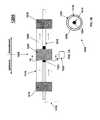
- FIGS. 1A-Ba set of simplified diagrams of a plasma reactor is shown, in accordance with the invention.
- FIG. 1Ashows a simplified schematic side diagram
- FIG. 1Bshows a simplified cross-sectional diagram.
- the plasma reactorincludes an inner electrode, an inner dielectric layer over the inner electrode, an outer dielectric layer over the inner dielectric layer, and an outer electrode over at least a portion of the outer dielectric layer.
- a channelis defined between an outer surface of the inner electrode and a surface of the outer electrode facing the outer surface of the inner electrode, which is referred to herein as an “inner surface” of the outer electrode.
- the channeldefines a plasma reactor chamber of the plasma reactor.
- the outer electrodeis disposed around and is in coaxial relation to the inner electrode. In such a case, an annular channel is defined between the outer surface of the inner electrode and the inner surface of the outer electrode.
- nanoparticlesmay be produced by continuously flowing one or more Group IV nanoparticle precursor gases (also referred to as “nanoparticle precursor gases” herein) into the plasma reactor chamber and forming (or igniting) a plasma of the nanoparticle precursor gases in the plasma reactor chamber by applying RF power to either the inner or outer electrode of the plasma reactor.
- Group IV nanoparticle precursor gasesalso referred to as “nanoparticle precursor gases” herein
- the inner electrodemay be in contact with the inner dielectric layer and the outer electrode may be in contact with at least a portion of the outer dielectric layer.
- the inner dielectric layeris separated from the outer dielectric layer such that a space is formed between the inner and outer dielectric layers.
- the spacedefines a channel, which is also referred to as a plasma reactor chamber of the plasma reactor.
- One or more Group IV nanoparticle precursor gasesare directed through the plasma reactor chamber.
- the plasma reactoris tubular. That is, the inner and outer dielectric layers are tubular or tube like.
- the inner dielectric tubecircumscribes the inner electrode
- the outer dielectric tubecircumscribes the inner dielectric tube
- the outer electrodecircumscribes the outer dielectric tube.
- the space between the inner and outer dielectric tubesdefines an annular channel.
- Plasma reactor 1200also referred to herein as a “concentric electrode” plasma reactor, comprises an inner electrode 1224 ; an inner dielectric tube 1215 circumscribing the inner electrode 1224 ; an outer dielectric tube 1214 disposed around and in coaxial relation with the inner dielectric tube 1215 , wherein an annular channel is defined between an outer surface of the inner dielectric tube 1215 and an inner surface of the outer dielectric tube 1214 ; and an outer electrode 1225 disposed around (or circumscribing) at least a portion of the outer dielectric tube.
- the inner dielectric tube 1215can be in contact with an outer surface of the inner electrode 1224 .
- the outer electrode 1225is disposed over an outer surface of the outer dielectric tube 1214 .
- the outer electrode 1225can be in contact with at least a portion of the outer surface of the outer dielectric tube 1214 .
- the inner electrode 1224 and outer electrode 1225collectively define an electrode assembly 1220 of the plasma reactor 1200 .
- the plasma reactor 1200can comprise a plurality of electrode assemblies 1220 .
- An annular channeldefines a plasma reactor chamber 1205 .
- the inner electrode 1224is rod shaped.
- the inner electrode 1224can have various geometric shapes and sizes.
- the inner electrode 1224can be rectangular.
- the inner 1215 and outer 1214 dielectric tubesare preferably formed of a dielectric material, such as quartz.
- the dielectric tube 1214forms the outer wall of the plasma reactor chamber 1205 of the plasma reactor 1200 .
- the plasma reactor chamber 1205provides a flow path for nanoparticle precursor gases.
- the plasma reactor chamber 1205may be sealed from the ambient atmosphere by flanges 1218 and 1219 at opposing ends of the plasma reactor 1200 .
- the dielectric tube 1215prevents sputtering of the inner electrode 1224 when the plasma reactor 1200 is in operation. This advantageously prevents contamination of the nanoparticles with material that forms the inner electrode 1224 .
- nanoparticle precursor gasesflow from the upstream end of the plasma reactor 1200 toward the downstream end of the plasma reactor 1200 .
- Plasma of the nanoparticle precursor gasesis formed in a reaction zone of the plasma reactor chamber 1205 .
- the reaction zoneis an area in the plasma reactor chamber 1205 that is defined by the inner 1224 and outer 1225 electrodes, in addition to the RF power density.
- the RF power densityis a function of the separation distance between the surfaces of the inner electrode 1224 and outer electrode 1225 , as well as the disposition of the inner electrode 1224 in relation to the outer electrode 1225 .
- nanoparticle precursor gas moleculesdissociate to form plasma-excited species of the nanoparticle precursor gas molecules. At least some of the plasma-excited species of the nanoparticle precursor gas molecules may nucleate and grow into Group IV nanoparticles.
- the nanoparticle precursor gasesare desirably mixed with a buffer gas that acts as a carrier gas.
- the buffer gasis typically an inert gas with a low thermal conductivity.
- the buffer gascomprises one or more inert gases selected from the group consisting of He, Ne, Ar, Kr, Xe and N 2 .
- the nanoparticle precursor gasesmay contain precursor molecules that dissociate to provide precursor species that react to form nanoparticles with a desired composition.
- the nanoparticle precursor gases directed into the plasmas reactor chamberwill depend on the type of nanoparticles desired. For example, if Group IV semiconductor nanoparticles are desired, one or more nanoparticle precursor gases having Group IV semiconductor elements are used.
- the one or more nanoparticle precursor gasesmay include one or more semiconductor precursor gases (e.g., SiH 4 , Si 2 H 6 ) and one or more dopant gases (e.g., PH 3 , B 2 H 6 ).
- the reaction zonecan span the length of the plasma reactor chamber 1205 .
- the reaction zoneis a function of the width of the outer electrode 1225 and the RF power density. To a rough approximation, the reaction zone spans a portion of the plasma reaction chamber 1205 in-between the inner electrode 1224 and outer electrode 1225 ; it can be about as wide as the outer electrode 1225 .
- plasma of the nanoparticle precursor gasesis formed in the reaction zone, and nanoparticles are formed, at least in part, in the reaction zone.
- nanoparticlesare formed solely in the reaction zone.
- plasma reactor 1200may comprise multiple reaction zones, in which case plasma of nanoparticle precursor gases is formed in each of the reaction zones. This may be of advantage in the formation of core-shell nanoparticles.
- nanoparticles with different materials to produce core-shell structuresare currently an active area of research, because such coating allows modification and tailoring of physical and chemical properties of core materials.
- SiNor other passivating agent
- Such graftingmay provide a method to reduce the amount of oxygen and carbon in the sintered film by reducing the amount of potential attachment sites on the nanoparticle.
- semiconductor nanoparticlestypically must be formed into dense connected regions in order to create a useful structure, such as a junction.
- One such methodis sintering.
- a method for making particlesadhere to each other, interacting nanocrystals sinter before size-dependent melting occurs.
- Group IV nanoparticlesalso tend to be very susceptible to contamination.
- contaminationoften occurs from such chemical reactions such as oxidation and/or hydrolysis. Consequently, even small amounts of contamination may inhibit sintering (i.e., interfering with the physical connection of the Group IV nanoparticles), delay dense layer formation (i.e., increasing material porosity and thus decreasing conductivity), and provide electron-hole recombination sites (i.e., attenuating current generation in the assembled junction).
- Plasma reactor 1200may further include inner electrode 1224 that can extend along a substantial portion of the plasma reactor 1200 .
- the inner electrode 1224can have a length that is equal to or smaller than the length of the outer electrode 1225 .
- the inner electrode 1224may be grounded 1226 and the outer electrode 1225 may be connected to an RF power source 1222 .
- the outer electrode 1225is grounded and the inner electrode 1224 is connected to the RF power source 1222 .
- the inner electrodeis grounded using a grounding wire 1226 (e.g., copper wire) that is in electrical contact with the inner electrode 1224 .
- the grounding wiremay be an RF shielded wire that is covered with a dielectric material.
- the grounding wire 1226may be disposed within the dielectric tube 1215 .
- One or more nanoparticle precursor gasesmay be introduced into the annular channel from a precursor gas source in fluid communication with an inlet port (not shown) of the plasma reactor 1200 .
- nanoparticles produced in the plasma reactor chambermay exit through an exit port (not shown) and into a nanoparticle collection chamber (not shown).
- the nanoparticlesmay be collected on a substrate or grid disposed within the plasma reactor chamber 1205 .
- Inner 1224 and outer 1225 electrodesmay be formed of any electrically conductive material, such as, e.g., gold, copper, or stainless steel.
- the inner electrode 1224 , the outer electrode 1225 , or bothmay be formed of a conductive material formed over an insulating material.
- the outer electrode 1225may be a gold or copper film sputtered over the outer dielectric tube 1214 . In such a case, sputtering may be controlled so as to define the width of the outer electrode 1225 .
- the dielectric tubes 1214 and 1215may be formed of any electrically insulating material, such as, e.g., quartz, sapphire, fumed silica, polycarbonate alumina, silicon nitride, or borosilicate glass.
- the inner electrode 1224may be insulated from the plasma reactor chamber 1205 using an insulating layer deposited on the inner electrode 1224 .
- a quartz layermay be formed over the inner electrode 1224 via chemical vapor deposition (CVD), atomic layer deposition (ALD), physical vapor deposition (PVD), or any other method capable of forming the quartz layer.
- the throughput of the plasma reactor 1200will scale with the radius of the annular channel defining the plasma reactor chamber 1205 .
- the diameters of the inner 1224 and outer electrodes 1225may be adjusted to enable a desired throughput.
- the separation distance between the outer surface of the inner electrode 1224 and the inner surface of the outer electrode 1225should be selected to provide a substantially uniform power density across the annular channel.
- the separation distancewill depend, at least in part, on the RF power.
- the RF powershould be scaled with the separation distance to enable a uniform power density in the reaction zone of the plasma reactor chamber 1205 . If a wide separation distance is desired, a relatively high RF power will have to be used to provide a substantially uniform power density.
- the separation distance between the surfaces of the inner 1224 and outer 1225 electrodesis not greater than about 30 mm. In some configurations, the separation distance is preferably between about 1 mm and about 60 mm, more preferably between about 5 mm and about 20 mm, and most preferably between about 8 mm and about 15 mm. In some configurations, plasma reactors configured for commercial-scale operation can have separation distances between about 40 and about 50 mm.
- the electrode assemblycomprises an elongated, rod-shaped (cylindrical) inner electrode 1224 and a shorter cylindrical outer electrode 1225 , with the downstream end (i.e., end downstream of the nanoparticle precursor gas flow, as indicated by the arrows) of the inner electrode 1224 not aligned from the downstream end of the outer electrode 1225 , other electrode configurations are possible.
- the downstream end of the inner electrode 1224is aligned with the downstream end of the outer electrode 1225 . This configuration can limit plasma generation to the confines of the downstream ends of the inner 1224 and outer electrodes 1225 , resulting in a more uniform power density and, hence, a higher degree of crystallinity in nanoparticles.
- inner electrode 1224 and the outer electrode 1225have substantially the same lengths, and their downstream and upstream ends are substantially aligned. This configuration produces a plasma reaction zone with sharper downstream and upstream edges, providing a power density distribution that may improve the crystallinity of the nanoparticles produced in the reaction zone.
- any wire attached to the downstream or upstream end of the inner electrode 1224may be electrically shielded so as to not affect the power density of the reaction zone in the plasma reactor chamber 1205 .
- Radiofrequency energy source 1222is generally in electrical communication (or electrical contact) with and supplies radiofrequency power to one of the electrodes.
- the other electrodeis grounded 1226 with a grounding wire in electrical contact with the other electrode.
- the RF power sourceis shown in electrical contact with the outer electrode 1225 and the inner electrode 1224 grounded 1226 , these connections could be reversed.
- the RF power source 1222may operate at various band frequencies, such as, e.g., the commercially available band frequency of about 13.56 MHz.
- plasma reactor 1200may comprise a plurality of inner electrodes and/or a plurality of outer electrodes.
- the plasma reactor 1200may include two or more inner electrodes and/or two or more outer electrodes laterally disposed in relation to one another.
- the inner and/or outer electrodesmay be in electrical contact (or electrical communication) with one another.
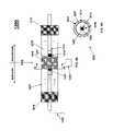
- FIG. 2a simplified diagram of plasma reactor 1200 comprising two separate outer electrodes is shown, in accordance with the invention.
- a first outer electrode 1221 and a second outer electrode 1231are disposed adjacent one another.
- the outer electrodes 1221 , 1231are generally in electrical contact with the RF power source 1222 .
- plasma reactor 1200comprises an inner electrode 1224 running the length of the plasma reactor 1200 .
- outer electrodes 1221 , 1231are generally positioned such that their plasma reaction zones overlap when the plasma reactor 1200 is in operation.
- the outer electrodes 1221 , 1231are positioned such that their plasma reaction zones do not overlap.
- nanoparticle precursor gasesmay be directed into the plasma reactor chamber 1205 downstream of the first outer electrode 1221 , and one or more nanoparticle precursor gases may be directed into the plasma reactor chamber 1205 through a conduit 1235 downstream of the first outer electrode 1221 and upstream of the second outer electrode 1231 .
- the plasma reactor 1200may comprise one outer electrode and a plurality of inner electrodes, the inner electrodes being in electrical contact with one another through electrically-insulated wires.
- the plasma reactor 1200may comprise a plurality of inner electrodes and a plurality of outer electrodes, with the electrodes positioned so as to produce a reaction zone having a power density distribution as desired when RF power is supplied to either the inner or outer electrodes.
- the plasma reactor 1200may include two outer electrodes and two inner electrodes; the electrodes having substantially equivalent widths; each outer electrode being substantially aligned with an inner electrode; the inner electrodes being in electrical contact with one another and grounded via electrically-insulated wires; and the outer electrodes being in electrical contact with the RF power source 1222 .
- either the first outer electrode 1221 or the second outer electrode 1231may be in electrical contact with the RF power source 1222 while the other outer electrode, in addition to the inner electrode 1224 , can be grounded 1226 .
- the first outer electrode 1221can be connected to the RF power source 1222
- the second outer electrode 1231 and inner electrode 1223can be grounded 1226 .
- Such a plasma reactor designcan confine the reaction zone, enabling the formation of more crystalline nanoparticles.
- This alternative configurationhelps to produce a stable and uniform plasma compared to the prior art dual-ring type plasma reactor. With proper combinations of electrodes and plasma parameters, a complete clean reaction zone (i.e., there is no film deposition within the reaction zone) is possible. Such a plasma reactor could be operated for a longer time period (without servicing) than the prior art dual-ring type plasma reactor.
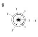
- plasma reactor 1300comprises a plurality of concentric annular channels formed in-between a plurality of electrodes arranged concentrically about a central, longitudinal axis.
- the electrodesare preferably insulated from the annular channels via electrically insulating (dielectric) tubes.
- a plurality of rod- or cylinder-shaped electrodes 1301 , 1302 , 1303 , 1304 , 1305 and 1306may be arranged in a coaxial relationship with the innermost electrode 1301 , with the innermost electrode 1301 having the smallest diameter and the outermost electrode 1306 having the largest diameter.
- the electrodesare alternately connected to an RF power source 1320 and grounded 1326 .
- Electrodes 1301 , 1303 and 1305are generally in electrical contact with ground 1326
- electrodes 1302 , 1304 and 1306are generally in electrical contact with the RF power source 1320 .
- Annular channels 1310 , 1311 , 1312 , 1313 and 1314are defined between each pair of electrodes.
- the resultis an electrode assembly with a plurality of coaxial plasma reaction chambers and plasma reaction zones that may be operated simultaneously to increase throughput and maximize nanoparticle production.
- the electrodesare insulated from the annular channels 1310 , 1311 , 1312 , 1313 and 1314 using a dielectric material (e.g., quartz) to avoid contaminating the nanoparticles when RF power is supplied to electrodes 1302 , 1304 and 1306 .
- a dielectric materiale.g., quartz
- At least one of the dielectric tubes 1214 and 1215 separating the electrodes from the plasma reactor chamber 1205is etched or sputtered, leading to contamination of the nanoparticles.
- Such etching or sputteringis more pronounced at higher RF powers.
- the dielectric tubes 1214 , 1215 of FIGS. 1A and 1Bare formed of quartz and silane (SiH 4 ) is used as a nanoparticle precursor gas, when RF power is supplied to the outer electrode 1225 to being nanoparticle production, silicon oxide can be etched or sputtered from the surfaces of at least one of the dielectric tubes 1214 , 1215 in the vicinity of the reaction zone. This can lead to contamination of the silicon nanoparticles.
- crackscan expose the inner electrode 1224 and/or the outer electrode 1225 to the plasma reactor chamber 1205 .
- RF poweris supplied to the outer electrode 1225 (the inner electrode 1224 is grounded 1226 ) and silane is used as a nanoparticle precursor gas
- crackscan form in dielectric tube 1215 circumscribing the inner electrode 1224 .
- formation of cracks in the dielectric tubes 1214 , 1215is reduced by alternately applying RF power to the inner electrode 1225 and outer electrode 1224 .
- RF poweris applied to the outer electrode 1225 while the inner electrode 1224 is grounded 1226 , and nanoparticles are formed when nanoparticle precursor gases are introduced into the plasma reactor chamber 1205 .
- Nanoparticle generationis then terminated by shutting off the RF power source and stopping the flow of nanoparticle precursor gases.
- RF poweris supplied to the inner electrode 1224 while the outer electrode 1225 is grounded, and nanoparticles are formed when nanoparticle precursor gases are introduced into the plasma reactor chamber 1205 .
- Nanoparticle generationis then terminated by shutting off the RF power source and stopping the flow of nanoparticle precursor gases. Cycles one and two may be repeated as required to provide a desired yield of nanoparticles. While this method would reduce the rate at which cracks are formed in the dielectric tubes 1214 , 1215 , it would not eliminate the etching or sputtering of the dielectric tubes 1214 , 1215 . In general, providing a dielectric sleeve over the dielectric tube 1215 and/or a dielectric sleeve below the dielectric tube 1214 aids in reducing, if not eliminating, degradation of one or both of the dielectric tubes 1214 , 1215 .
- plasma reactor 1200comprises a tubular dielectric sleeve 1216 disposed over the dielectric tube 1215 and positioned in the reaction zone.
- the dielectric sleeve 1216is preferably removable.
- the dielectric sleeve 1216may have a wall thickness between about 4 mm and about 10 mm.
- etching or sputtering of the dielectric tube 1215is reduced, in not eliminated, when the dielectric sleeve 1216 is disposed around the dielectric tube 1215 and in the reaction zone.
- the dielectric sleeve 1216may be removed and replaced with another sleeve. This advantageously minimizes downtime, leading to lower operating costs. Use of the dielectric sleeve 1216 advantageously resolves problems associated with the formation of cracks in the dielectric tube 1215 .
- the dielectric sleeve 1216may be formed of any dielectric material, such as, e.g., quartz, silicon nitride, or silicon carbide.
- the dielectric sleeve 1216may be coated with a layer of a material having a reduced etch rate with respect to the etch rate of the underlying dielectric material. In general, this tends to eliminate nanoparticle contamination, as described above.
- the dielectric sleeve 1216can be coated with a layer of any material having a reduced etch rate relative to the material comprising the dielectric sleeve 1216 .
- a silicon nitride (Si x N y , wherein x>0 and y>0) layer or a layer of a Group IV semiconductorcould be used.
- the layer of material having a reduced etch ratemay be deposited over the dielectric sleeve 1216 ; it may have a thickness between about 50 nm and about 2000 nm.
- Plasma reactor 1200may comprise a dielectric sleeve 1217 disposed below the dielectric tube 1214 and laterally positioned in the reaction zone.
- the dielectric sleeve 1217can protect portions of the dielectric tube 1214 in the reaction zone from etching during nanoparticle formation.
- the dielectric sleevemay be useful in cases where RF power is applied to the inner electrode 1224 while the outer electrode 1225 is grounded 1226 .
- the dielectric sleeve 1217preferably has a smaller radius than the dielectric tube 1214 .
- both the dielectric tube 1214 and the dielectric sleeve 1217may be formed of quartz, and the surface of the dielectric sleeve 1217 that is in contact with the plasma reactor chamber 1205 may be coated with silicon nitride.
- Plasma reactor 1200can comprise both dielectric sleeves 1216 and 1217 , as illustrated.
- the dielectric sleeves 1216 and 1217may be formed of a material having an etch rate that is lower than the etch rate of the dielectric tubes 1214 , 1215 .
- the dielectric sleeves 1216 and 1217may be formed of material selected from the group consisting of Group IV semiconductors, sapphire, polycarbonate alumina, silicon nitride (Si x N y , wherein x>0 and y>0), silicon carbide and borosilicate glass.
- the dielectric sleeves 1216 , 1217may be formed of a first material, and surfaces of the dielectric sleeves 1216 , 1217 that are exposed to the plasma reactor chamber 1205 may be coated with a material (e.g., silicon nitride) having an etch rate that is lower than the etch rate of the material of the dielectric sleeves 1216 , 1217 .
- a materiale.g., silicon nitride
- dielectric sleeves 1216 , 1217is advantageous in cases where, for example, RF power is alternately applied to the inner 1224 and outer 1225 electrodes (see above).
- dielectric sleevesmay be provided in each of the reaction zones, as discussed above.
- the contamination of nanoparticles with the material of the dielectric tubes 1214 , 1215may be substantially reduced by the application of RF power selected so as to reduce the etching of the dielectric tubes 1214 , 1215 .
- RF powerselected so as to reduce the etching of the dielectric tubes 1214 , 1215 .
- the higher the RF powerthe higher the etching rate.
- operating the plasma reactor 1200 with a low RF powermay substantially reduce etching of the dielectric tubes 1214 , 1215 .
- the flow rate of nanoparticle precursor gaseswould have to be adjusted accordingly, and the plasma reactor 1200 may be operated for a longer period of time to provide a desired yield of nanoparticles.
- a plurality of plasma reactorsmay be operated in parallel to give a desired nanoparticle yield.
- RF powermay be alternately applied to the inner and outer electrodes, as described above, in order to reduce the formation of cracks in the dielectric tubes 1214 , 1215 .
- one or both of the dielectric tubes 1214 , 1215may be formed of a material that is substantially resistant to etching, and thus substantially reduce crack formation in dielectric tubes 1214 , 1215 , as well as nanoparticle contamination.
- RF poweris applied to the outer electrode 1225 while the inner electrode 1224 is grounded 1226 , and the dielectric tube 1215 is formed of a material substantially resistant to etching.
- RF poweris applied to the inner electrode 1224 while the outer electrode 1225 is grounded, and the dielectric tube 1214 is formed of a material substantially resistant to etching.
- both of the dielectric tubes 1214 , 1215are formed of a material substantially resistant to etching.
- Material that is substantially resistant to etchinghas an etching (or sputtering rate) that is at least 35 times lower than the etching (or sputtering) rate of silicon oxide.
- material that is substantially resistant to etchingis selected from group consisting of Group IV semiconductors, sapphire, polycarbonate alumina, silicon nitride (Si x N y , wherein x>0 and y>0), silicon carbide and borosilicate glass.
- FIG. 5a schematic cross-sectional side view of a plasma reactor is shown having protective layers over portions of the dielectric tubes of the plasma reactor, in accordance with the invention.
- One or both of the dielectric tubes 1214 , 1215may be formed of a first material, and the surfaces of one or both of the dielectric tubes 1214 , 1215 that are in contact with the plasma reactor chamber 1205 and laterally disposed in the reaction zone may be covered with one or more layers of a second material 1229 , wherein the second material has a lower etch rate than the first material.
- the layer of the second material 1229substantially covers portions of one of both of the dielectric tubes 1214 , 1215 in the reaction zone of the plasma reactor chamber 1205 .
- the first materialmay be a low-cost material, such as, e.g., quartz (SiO x ), and the second material may be selected from the group consisting of Group IV semiconductors, sapphire, polycarbonate alumina, silicon nitride (Si x N y , x>0, y>0), silicon carbide and borosilicate glass.
- the one of more layers of the second material 1229 over portions of one or both of the dielectric tubes 1214 , 1215 in the reaction zonehas a thickness preferably between about 50 nm and about 2000 nm.
- the dielectric tubes 1214 , 1215 in the reaction zoneare both covered with a layer of the second material 1229 , it will be appreciated that the layer of the second material 1229 can be provided over only one of the dielectric tubes 1214 , 1215 . As described above, the layer of the second material 1229 provides a protective coating to prevent etching of one or both of the dielectric tubes 1214 , 1215 during nanoparticle formation.
- the layer of the second material 1229may be formed by directing precursor gases of the second material through the plasma reactor chamber 1205 and applying RF power to the inner electrode 1224 , the outer electrode 1225 , or both in sequence.
- layers of the second material 1229 over one or both of the dielectric tubes 1214 , 1215may be formed by flowing N 2 (or ammonia) and a silicon precursor (e.g., SiH 4 ) through the plasma reactor chamber 1205 , and by applying RF power to either the inner electrode 1224 , the outer electrode 1225 , or both in sequence.
- RF poweris preferably applied to the outer electrode 1225 and the inner electrode 1224 is grounded 1226 .
- RF poweris preferably applied to the inner electrode 1224 and the outer electrode 1225 is grounded 1226 .
- RF powermay be applied to both electrodes in sequence. That is, while flowing the silicon nitride precursor gases, RF power can be applied to one electrode (e.g., the inner electrode 1224 ) while the other electrode (e.g., the outer electrode 1225 ) is grounded 1226 , and after a predetermined time period (see below), RF power can be applied to the other electrode (e.g., the outer electrode 1225 ) while the electrode that was previously connected to the RF power source 1222 is grounded 1226 .
- one electrodee.g., the inner electrode 1224
- the other electrodee.g., the outer electrode 1225
- the electrode that was previously connected to the RF power source 1222is grounded 1226 .
- the silicon nitride precursor gasese.g., N 2 or NH 3 , and SiH 4
- the RF power used for forming the silicon nitride coating (or layer)is between about 1 W and 50 W, more preferably between about 1 W and 30 W, and most preferably between about 1 W and 25 W.
- the time period for forming the silicon nitride layeris preferably between about 1 minute and about 20 minutes, more preferably between about 1 minute and about 15 minutes, and most preferably between about 1 minute and about 10 minutes.
- the entire reactor 1200is preferably annealed while the silicon nitride coating is applied. For example, reactor 1200 may be annealed by wrapping the reactor 1200 with resistive heating tape and applying power to the heating tape.
- heating tapesmay be used to anneal the reactor 1200 .
- the reactor 1200is annealed at a temperature preferably between about 100° C. and about 500° C., more preferably between about 150° C. and about 400° C., and most preferably between about 200° C. and 300° C.
- the silicon nitride layeris preferably annealed after it is applied to the dielectric tube 1214 or 1215 (or dielectric sleeve 1216 or 1217 , if used).
- the silicon nitride coatingis annealed at a temperature preferably between about 250° C. and about 700° C., more preferably between about 350° C. and about 600° C., and most preferably between about 450° C. and 550° C., and annealed for at time period preferably between about 1 minute and 60 minutes, more preferably between about 10 minutes and 50 minutes, and most preferably between about 20 minutes and 35 minutes.
- Group IV nanoparticlessuch as Group IV semiconductor nanoparticles, may then be produced using the plasma reactor 1200 having a layer of silicon nitride applied the dielectric tube 1214 or 1215 (or dielectric sleeve 1216 or 1217 ). It will be appreciated that preferred methods enable formation of a silicon nitride layer over portions of a dielectric tube in the reaction zone. That is, with RF power provided to either the inner electrode 1224 or outer electrode 1225 , excited species of the silicon nitride precursor gases are formed in the reaction zone and react to form a layer of silicon nitride over portions of one or both of the dielectric tubes 1214 , 1215 in the reaction zone.
- the RF and ground configurationcan be alternated (as described above).
- applying RF power to the outer electrode 1225 while the inner electrode 1224 is groundedproduces silicon nitride layer over the dielectric tubes 1214 and 1215 .
- RF parametersmay be adjusted to yield a silicon nitride layer with a desired thickness.
- the layer of the second material 1229may be formed of other materials, such as, e.g., borosilicate glass.
- a layer of the second material 1229is to be applied to both dielectric tubes 1214 , 1215 (or dielectric sleeves 1216 , 1217 ), different materials may be applied over each dielectric tube (or sleeve).
- the layer of the second material over the dielectric tube 1215is formed of silicon nitride
- the layer of the second material over the dielectric tube 1214can be formed of borosilicate glass.
- the methods described above for forming a layer of a second material over the dielectric tubescan be applied to a plasma reactor having a plurality of reaction zones.
- FTIRFourier transform infrared
- Dielectric tubes 1214 , 1215were formed of quartz (SiO x ). Without the silicon nitride coating, the FTIR spectra of the nanoparticle powders displayed a broad silicon oxide-related peak slightly above 1000 cm ⁇ 1 . This indicates that during nanoparticle production, portions of one or both of the dielectric tubes 1214 , 1215 were etched or sputtered into the gas phase and incorporated into the nanoparticles.
- FTIR spectra of nanoparticle powders formed using a reactor with the silicon nitride coatingdid not exhibit the silicon oxide-related peak, indicating that the problem associated with nanoparticle contamination had been eliminated.
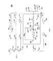
- FIG. 7shows a simplified plasma reactor system configured for forming Group IV semiconductor or metal nanoparticles, in accordance with the invention.
- the plasma reactor system 100includes a plurality of nanoparticle precursor gas lines, which define a nanoparticle precursor gas manifold 150 .
- Gas line 130is comprised of a gas source 131 , a gas line trap 132 for scrubbing oxygen and water from the gas, a gas line analyzer 134 for monitoring oxygen and water concentrations to ensure that they are within desired levels, a gas line flow controller 135 , and a gas line valve 137 . All elements comprising the gas line 130 are in fluid communication with one another through gas line conduit 133 .
- Gas line 130could be used as, e.g., a nanoparticle precursor gas line.
- the nanoparticle precursor gases passesmay include primary nanoparticle precursor gases, nanoparticle dopant gases, nanoparticle core precursor gases, nanoparticle shell precursor gases, buffer gases, and combinations thereof.
- gas line trap 132is optional for scrubbing oxygen and water from the dopant gas in cases where the dopant gas is not reactively aggressive and can be effectively filtered.
- gas line analyzer 134may be used if the dopant gas is not reactively aggressive. If the dopant gas is reactively aggressive, gas line trap 132 and gas line analyzer 134 may be omitted. This is shown in gas lines 110 and 120 , which include gas sources 111 and 121 , conduits 113 and 123 , gas line flow controllers 115 and 125 and gas line valves 117 and 127 .
- gases from lines 110 , 120 , 130are in fluid communication with a plasma reactor 500 through inlet line 210 , which includes an inlet line valve 212 .
- Nanoparticle precursor gases and buffer gasesare introduced into the plasma reactor 500 through an inlet port of a plasma reactor 500 and flow continuously through a plasma reactor chamber and a reaction zone of the plasma reactor 500 defined in part by an electrode assembly 520 , where nanoparticles are formed.
- RF poweris supplied by an RF power source 522 .
- the resulting nanoparticlesare then collected in a nanoparticle collection chamber 330 .
- the collection chamber 330may be located downstream of the plasma reactor 500 .
- the nanoparticle collection chamber 330may comprise, e.g., a grid or mesh configured for collecting nanoparticles. Nanoparticles may be directed to the nanoparticle collection chamber 330 via an outlet port of the plasma reactor 500 . In general, nanoparticles exit the plasma reactor 500 and flow into outlet line 310 . The nanoparticles may be collected in nanoparticle collection chamber 330 , which is separated from the plasma reactor 500 by valve 312 .
- the effluent gase.g., unreacted nanoparticle precursor gases, dopant gases, carrier gases
- a valve 332is located downstream of the nanoparticle collection chamber 330 .
- collection chamber 330may consists of an air tight collection chamber configured to exclude ambient air down to a pressure range of about 10 millitorr.
- automated devices intrinsic to the collection operations performed by the collection chamber 330may be controlled via a programmable automation controller (PAC).
- PACprogrammable automation controller
- the collection chamber 330may further be configured with inlet and outlet ports.
- a filter membrane with a vibrating devicemay be mounted diagonally within the chamber in such a way as to force all gas and particulate entering the chamber via the inlet port to pass through the filter membrane before exiting via the outlet port.
- a pressure sensormay activate the vibrating device affixed to the filter media to dislodge trapped particulate matter.
- the lower part of the chambermay be a collection hopper where particles dislodged from the membrane are collected.
- the hoppermay also have vibrating devices and a dual valve assembly which opens when the hopper fills, allowing the collected material to fall through the bottom of the hopper into a fixed processing vessel.
- the chambermay further have one or more oxygen sensors that serve as part of a safety device. In general, if oxygen levels within the collection chamber exceed a predetermined safe limit, a controller will initiate a sequence to isolate and flood the chamber with inert gas to prevent hazardous reaction within the chamber.
- Plasma reactor 500may be any plasma reactor capable of forming Group IV nanoparticles.
- the plasma reactor 500can be any one of the plasma reactors described above in the context of FIGS. 1-5 .
- the plasma reactor 500can be a dual-ring type plasma reactor, such as the dual-ring type plasma reactor described in U.S. Patent Publication No. 2006/0051505.
- Pressure in the nanoparticle collection chamber 330may be regulated by a pressure control system, which is comprised of a pressure sensor 320 , controller 322 , a throttle valve 324 and an exhaust assembly 400 .
- the throttle valve 324may be a butterfly valve, for example.
- inlet valve 312 and outlet valve 332are open, and the throttle valve 324 is partially open.
- Controller 322decreases the pressure in the nanoparticle collection chamber 330 by opening the butterfly valve 324 to increase the flow rate of gas out of the nanoparticle collection chamber 330 .
- Downstream of the nanoparticle collection chamber 330is an exhaust assembly 400 , which includes an exhaust line 410 , particle trap 414 , and pump 430 having a mist trap 434 .
- the plasma reactor 500 and, optionally, the precursor gas manifold 150 and the nanoparticle collection chamber 330may be disposed within a sealed, inert environment, such as, e.g. a glovebox.
- inert environmentdescribes a chemically unreactive background environment devoid of gases, solvents, and/or solutions that are capable of reacting with other gases and nanoparticles formed in the plasma reactor 500 .
- the inert environmentpreferably does not adversely affect electrical, photoelectrical, and luminescent properties of the nanoparticles.
- Inert gases, solvents and solutionspreferably do not react with the nanoparticles so as to adversely affect the physical properties of the nanoparticles.
- an inert environmentis established by backfilling an enclosure having the nanoparticle reactor chamber and the nanoparticle collection chamber with an inert gas (e.g., N 2 , Ar, He).
- the inert gas pressuremay be regulated to ensure that the pressure of inert gas in the enclosure is maintained at a desirable level.
- an inert environmentis established by keeping the enclosure under vacuum.
- inert gasesexamples include nitrogen and noble gases, such as, e.g., Ar and He.
- the inert environmentis substantially oxygen free.
- substantially oxygen freerefers to an environment having gases, solvents, and/or solutions in which the oxygen content has been reduced to minimize, if not eliminate, the oxidation of the nanoparticles that come in contact with the environment.
- the inventorshave observed that, in some cases, if the reactor 500 is opened after use, at least some of nanoparticle precursor species used during production of nanoparticles desorb from walls (or surfaces) of the reactor 500 that were exposed to nanoparticle precursor gases. This may pose health and safety issues if the desorbing gases are hazardous. As an example, after formation of n-type nanoparticles using PH 3 as a dopant precursor gas, after the reactor 500 was exposed to air, the concentration of PH 3 near the reactor 500 increased from an undetectable level to about 13 parts per million (“ppm”). Accordingly, there is a need for a method for removing nanoparticle precursor species from the surfaces of the reactor 500 exposed to nanoparticle precursor gases during nanoparticle production.
- nanoparticle precursor speciesmay be removed from the plasma reactor 500 by flowing (or directing) a cleansing gas through the plasma reactor 500 .
- the cleansing gasmay be directed through the plasma reactor 500 with the aid of a carrier gas provided upstream of the plasma reactor 500 and/or a vacuum provided downstream of the plasma reactor 500 .
- the cleansing gasmay react with the nanoparticle precursor species, removing them from the surfaces of the plasma reactor 500 exposed to nanoparticle precursor gases during nanoparticle formation.
- the cleansing gasneed not react with the nanoparticle precursor species.
- the effluent gasmay comprise the cleansing gas, the nanoparticle precursor species, the carrier gas, and combinations thereof.
- the effluent gasmay comprise a species that is formed upon reaction between a nanoparticle precursor species and the cleansing gas.
- the collection vesselis a trap, such as, e.g., a cold trap where the effluent gas condenses to form a liquid and/or a solid having at least some of the species in the effluent gas.
- the cleansing gascomprises one or more organic chemicals.
- the cleansing gasis selected from the group consisting of alcohols, carboxylic acids, aldehydes and ketones.
- the cleansing gasmay be isopropanol vapor provided with a carrier gas.
- the carrier gasinclude a noble gas (e.g., He, Ar, etc.), oxygen, nitrogen, hydrogen, or ambient air.
- the cleansing gasmay be directed through the plasma reactor 500 upon application of a vacuum downstream of the plasma reactor and/or upon application of a pressurized carrier gas upstream of the plasma reactor 500 .
- Nanoparticle precursor speciesgenerally refers to atoms and molecules adsorbed on walls of the plasma reactor 500 exposed to nanoparticle precursor gases during nanoparticle production (or formation). As an example, if PH 3 was used during nanoparticle formation, nanoparticle precursor species comprises PH 3 adsorbed on walls of the plasma reactor 500 exposed to PH 3 during nanoparticle formation. Nanoparticle precursor species may also be adsorbed on nanoparticles that are deposited on surfaces of the plasma reactor 500 exposed to the nanoparticles during nanoparticle formation.
- the plasma reactor 500may be any plasma reactor configured for forming nanoparticles.
- the plasma 500is the concentric electrode plasma reactor, such as the plasma reactor 1200 discussed (as shown in FIGS. 1A-B )
- nanoparticle precursor speciesmay adsorb on surfaces of the inner and outer dielectric tubes 1214 , 1215 of the plasma reactor 1200 .
- nanoparticle precursor speciesmay adsorb on nanoparticles deposited on walls (or surfaces) of the plasma reactor 500 exposed to nanoparticle precursor gases during nanoparticle formation.
- a nanoparticle precursor gas recovery systemcomprising a bubbler 600 in fluid communication with the plasma reactor 500 is shown.
- Valve 605isolates the bubbler 600 from a gas line that is directed into the plasma reactor 500 .
- the bubbler 600is in fluid communication with an inert gas supply or, alternatively, the ambient environment (e.g. air), via line 610 .
- bubbler 600is filled with a liquid preferably having protic solvent properties.
- the liquidmay be water, isopropanol or other alcohols, carboxylic acids, ketones, primary and secondly amines, ammonia.
- Line 610may comprise a valve 612 to seal the bubbler 600 from the ambient environment when the nanoparticle precursor gas recovery system is not in use.
- Bubbler 600generally provides the cleansing gas.
- the nanoparticle precursor gas recovery systemfurther comprises a nanoparticle precursor gas trap 615 (“trap”), which is configured to capture the effluent gas from the plasma reactor 500 .
- trap 615is a cold trap, such as, e.g., a liquid nitrogen-cooled trap.
- Valve 620isolates the nanoparticle collection chamber 330 from the trap 615 .
- Valve 625isolates the trap 615 from the plasma reactor 500 and the nanoparticle collection chamber 330 during operation of the plasma reactor 500 .
- the trap 615is in fluid communication with a vacuum source 630 , such as, e.g., a mechanical pump.
- a vacuum source 630such as, e.g., a mechanical pump.
- valve 620is generally open and valves 605 and 625 are generally closed, isolating the bubbler 600 and the trap 615 from the plasma reactor 500 .
- one or more nanoparticle precursor speciesmay be removed from the plasma reactor 500 by closing valves 212 and 620 , opening valves 605 , 612 and 625 , and applying vacuum to the trap 615 via the vacuum source 630 .
- the bubbler 600is in fluid communication with an inert gas source via line 610 , flow of inert gas may be initiated.
- the inert gas or air provided via line 610is directed (or bubbled) through the liquid in the bubbler 600 to form a cleansing gas comprising molecules of the liquid.
- the cleansing gasmay be directed into the plasma reactor 500 , where it removes one or more nanoparticle precursor species from the walls of the plasma reactor 500 exposed to one or more nanoparticle precursor gases during nanoparticle formation.
- the resulting effluent gasis subsequently directed into the trap 615 , where it is captured.
- valves 605 , 612 and 625are closed, and the trap 615 is removed and processed to dispose of the species collected in the trap 615 from the effluent gas. This may be carried out in a glove box (or an inert environment).
- the bubbler 600was filled with isopropanol; line 610 was in fluid communication with the ambient environment (i.e., air); the trap 615 was a liquid nitrogen cold trap; and the vacuum 630 was supplied by a mechanical pump (not shown). Valves 212 and 620 were open; valves 605 , 612 and 625 were closed.
- the plasma reactorwas the concentric electrode plasma reactor described above in the context of FIGS. 1A-B .
- the plasma reactorwas initially used to form n-type nanoparticles using, among other things, PH 3 as a dopant precursor gas. Formation of nanoparticles in the plasma reactor 500 was terminated by turning off the RF power supply 522 and terminating the supply of nanoparticle precursor gases. Thereafter, valves 212 and 620 were closed and valves 605 , 612 and 625 were opened.
- the air-isopropanol gas mixtureremoved PH 3 from the plasma reactor, and the resulting effluent gas was directed into the liquid nitrogen cooled trap 615 by the vacuum 630 , where the effluent gas condensed.
- valves 605 , 612 and 625were closed and the liquid nitrogen cold trap 615 was removed.
- the trap 615was taken to a glove box where species captured from the effluent gas was disposed of.
- the plasma reactor 500was then exposed to the ambient environment.
- the concentration of PH 3 measured near the reactor 500was less than 1 ppm.
- the nanoparticle precursor gas recovery systemcomprises a bubbler 600 for providing the cleansing gas
- the cleansing gasmay be provided by other means.
- the cleansing gasmay be provided by a pressurized canister having one or more chemicals capable of removing nanoparticle precursor species from surfaces of the plasma reactor 500 exposed to nanoparticle precursor gases during nanoparticle formation.
- a reactor 1200was used having inner and outer dielectric tubes 1215 and 1214 , respectively, formed of quartz.
- the outer dielectric tube 1214had an outer diameter of about 51 mm and an inner diameter of about 48 mm.
- the inner dielectric tube 1215had an outer diameter of about 19 mm and an inner diameter of about 17 mm.
- the inner and outer electrodes 1224 and 1225were formed of copper.
- the outer electrode 1225had a length of about 75 mm and an outer diameter of about 54 mm.
- the inner electrode 1224had an outer diameter of about 16 mm and a length of about 75 mm.
- RF powerwas applied to the outer electrode 1225 while the inner electrode 1224 was grounded 1226 .
- Silanewas directed into the plasma reactor 1200 at a flow rate of about 7.5 standard cubic centimeters per minute (sccm), N 2 (g) was directed into the plasma reactor at a flow rate of about 100 sccm, and the plasma reactor 1200 had a plasma reactor pressure (or plasma chamber pressure) of about 0.48 torr.
- RF powerwas applied at an RF power of about 15 W at an RF frequency of about 13.56 MHz.
- RF powerwas applied between about 10 minutes and 15 minutes.
- the silicon nitride layer (or film) formed over the inner dielectric tube 1215was annealed at about 500° C. for about 30 minutes.
- p-type silicon nanoparticles particleswere prepared in the plasma reactor described in Example 1.
- P-type silicon nanoparticleswere prepared by flowing a dopant gas comprising diborane and a Group IV semiconductor precursor gas comprising silane through the plasma reactor and applying RF power to the outer electrode.
- Diboranewas directed through the plasma reactor with the aid of an argon carrier gas.
- the concentration of diboranewas about 1000 ppm.
- the flow rate of the dopant gaswas about 160 sccm, and the flow rate of the Group IV semiconductor precursor gas was about 16 sccm, which provided a boron to silicon ratio of about 2.0% in the plasma reactor.
- the RF power delivered to the outer electrodewas about 78 W.
- the pressure in the plasma reactor chamberwas about 8 Torr.
- doped Group IV semiconductor thin filmswere formed from p-type silicon nanoparticles.
- the substrate used for p-type silicon thin filmswas a 1-inch by 1-inch by 0.04-inch quartz substrate.
- the quartz substratewas cleaned using an argon plasma.
- P-type silicon nanoparticleswere prepared using the plasma reactor described in Example 1.
- the silicon nanoparticle ink (or colloidal dispersion) used in the formation of the thin filmwas prepared in an inert environment using the p-type silicon nanoparticles.
- the inkwas formulated as a 20 mg/ml solution in 4:1 mixture (by volume) of chloroform and chlorobenzene, which was sonicated using a sonication horn at 35% power for 15 minutes.
- the inkwas used to substantially cover a surface of the quartz substrate, and a silicon nanoparticle porous compact was formed by spin casting the ink on the substrate at 1000 rpm for 60 seconds.
- a p-type silicon thin filmwas fabricated using a conditioning step comprising baking the porous compact at 100° C. for about 15 minutes at a pressure between about 5 ⁇ 10 ⁇ 6 and about 7 ⁇ 10 ⁇ 6 Torr using a 15 minute heating ramp. This was followed by heat treatment at a fabrication temperature of about 765° C.
- a densified doped Group IV semiconductor thin filmwas formed on the silicon substrate.
- the doped Group IV semiconductor thin filmhad a thickness between about 300 nm and about 350 mm.
- the electrode assemblies and plasma reactor chambers described aboveare readily incorporated into a larger plasma reactor system, which may include additional external components, such as a precursor gas inlet manifold, a nanoparticle collection manifold, and a pressure control system.
- a computer control systemcan be used to regulate the nanoparticle precursor gas flow rate, the pressure within the plasma reactor and the RF power source.
Landscapes
- Chemical & Material Sciences (AREA)
- Engineering & Computer Science (AREA)
- Organic Chemistry (AREA)
- Physics & Mathematics (AREA)
- Plasma & Fusion (AREA)
- Analytical Chemistry (AREA)
- Nanotechnology (AREA)
- Composite Materials (AREA)
- Health & Medical Sciences (AREA)
- General Health & Medical Sciences (AREA)
- Inorganic Chemistry (AREA)
- Chemical Kinetics & Catalysis (AREA)
- Condensed Matter Physics & Semiconductors (AREA)
- General Physics & Mathematics (AREA)
- Materials Engineering (AREA)
- Crystallography & Structural Chemistry (AREA)
- Toxicology (AREA)
- Physical Or Chemical Processes And Apparatus (AREA)
Abstract
Description
Claims (23)
Priority Applications (1)
| Application Number | Priority Date | Filing Date | Title |
|---|---|---|---|
| US12/113,451US8471170B2 (en) | 2007-07-10 | 2008-05-01 | Methods and apparatus for the production of group IV nanoparticles in a flow-through plasma reactor |
Applications Claiming Priority (2)
| Application Number | Priority Date | Filing Date | Title |
|---|---|---|---|
| US11/775,509US20090014423A1 (en) | 2007-07-10 | 2007-07-10 | Concentric flow-through plasma reactor and methods therefor |
| US12/113,451US8471170B2 (en) | 2007-07-10 | 2008-05-01 | Methods and apparatus for the production of group IV nanoparticles in a flow-through plasma reactor |
Related Parent Applications (1)
| Application Number | Title | Priority Date | Filing Date |
|---|---|---|---|
| US11/775,509Continuation-In-PartUS20090014423A1 (en) | 2006-12-21 | 2007-07-10 | Concentric flow-through plasma reactor and methods therefor |
Publications (2)
| Publication Number | Publication Date |
|---|---|
| US20090044661A1 US20090044661A1 (en) | 2009-02-19 |
| US8471170B2true US8471170B2 (en) | 2013-06-25 |
Family
ID=40361927
Family Applications (1)
| Application Number | Title | Priority Date | Filing Date |
|---|---|---|---|
| US12/113,451Active2031-06-01US8471170B2 (en) | 2007-07-10 | 2008-05-01 | Methods and apparatus for the production of group IV nanoparticles in a flow-through plasma reactor |
Country Status (1)
| Country | Link |
|---|---|
| US (1) | US8471170B2 (en) |
Cited By (20)
| Publication number | Priority date | Publication date | Assignee | Title |
|---|---|---|---|---|
| KR101386611B1 (en) | 2013-01-14 | 2014-04-17 | 한국에너지기술연구원 | Unit for trapping nano-particle and apparatus for manufacturing nano-particle having the same |
| RU2565182C1 (en)* | 2014-07-01 | 2015-10-20 | Федеральное государственное бюджетное учреждение науки Институт неорганической химии им. А.В. Николаева Сибирского отделения Российской академии наук | Method of producing nanosized powder of silicon compounds |
| WO2017190015A1 (en)* | 2016-04-29 | 2017-11-02 | Monolith Materials, Inc. | Torch stinger method and apparatus |
| US10100200B2 (en) | 2014-01-30 | 2018-10-16 | Monolith Materials, Inc. | Use of feedstock in carbon black plasma process |
| US10138378B2 (en) | 2014-01-30 | 2018-11-27 | Monolith Materials, Inc. | Plasma gas throat assembly and method |
| US10370539B2 (en) | 2014-01-30 | 2019-08-06 | Monolith Materials, Inc. | System for high temperature chemical processing |
| US10618026B2 (en) | 2015-02-03 | 2020-04-14 | Monolith Materials, Inc. | Regenerative cooling method and apparatus |
| US10808097B2 (en) | 2015-09-14 | 2020-10-20 | Monolith Materials, Inc. | Carbon black from natural gas |
| US11149148B2 (en) | 2016-04-29 | 2021-10-19 | Monolith Materials, Inc. | Secondary heat addition to particle production process and apparatus |
| US11304288B2 (en) | 2014-01-31 | 2022-04-12 | Monolith Materials, Inc. | Plasma torch design |
| US11453784B2 (en) | 2017-10-24 | 2022-09-27 | Monolith Materials, Inc. | Carbon particles having specific contents of polycylic aromatic hydrocarbon and benzo[a]pyrene |
| US11665808B2 (en) | 2015-07-29 | 2023-05-30 | Monolith Materials, Inc. | DC plasma torch electrical power design method and apparatus |
| US11760884B2 (en) | 2017-04-20 | 2023-09-19 | Monolith Materials, Inc. | Carbon particles having high purities and methods for making same |
| US11926743B2 (en) | 2017-03-08 | 2024-03-12 | Monolith Materials, Inc. | Systems and methods of making carbon particles with thermal transfer gas |
| US11939477B2 (en) | 2014-01-30 | 2024-03-26 | Monolith Materials, Inc. | High temperature heat integration method of making carbon black |
| US20240128059A1 (en)* | 2022-10-18 | 2024-04-18 | The Uab Research Foundation | Catalytic nanofiber membrane assembly and reduced pressure plasma reactor for fluid, vapor and gas processing |
| US11987712B2 (en) | 2015-02-03 | 2024-05-21 | Monolith Materials, Inc. | Carbon black generating system |
| US12030776B2 (en) | 2017-08-28 | 2024-07-09 | Monolith Materials, Inc. | Systems and methods for particle generation |
| US12119133B2 (en) | 2015-09-09 | 2024-10-15 | Monolith Materials, Inc. | Circular few layer graphene |
| US12378124B2 (en) | 2017-08-28 | 2025-08-05 | Monolith Materials, Inc. | Particle systems and methods |
Families Citing this family (21)
| Publication number | Priority date | Publication date | Assignee | Title |
|---|---|---|---|---|
| US8968438B2 (en)* | 2007-07-10 | 2015-03-03 | Innovalight, Inc. | Methods and apparatus for the in situ collection of nucleated particles |
| US20100037820A1 (en)* | 2008-08-13 | 2010-02-18 | Synos Technology, Inc. | Vapor Deposition Reactor |
| US20100037824A1 (en)* | 2008-08-13 | 2010-02-18 | Synos Technology, Inc. | Plasma Reactor Having Injector |
| US8851012B2 (en)* | 2008-09-17 | 2014-10-07 | Veeco Ald Inc. | Vapor deposition reactor using plasma and method for forming thin film using the same |
| US8770142B2 (en)* | 2008-09-17 | 2014-07-08 | Veeco Ald Inc. | Electrode for generating plasma and plasma generator |
| US8871628B2 (en)* | 2009-01-21 | 2014-10-28 | Veeco Ald Inc. | Electrode structure, device comprising the same and method for forming electrode structure |
| US8257799B2 (en)* | 2009-02-23 | 2012-09-04 | Synos Technology, Inc. | Method for forming thin film using radicals generated by plasma |
| US8758512B2 (en)* | 2009-06-08 | 2014-06-24 | Veeco Ald Inc. | Vapor deposition reactor and method for forming thin film |
| US20110209746A1 (en)* | 2009-09-06 | 2011-09-01 | Hanzhong Zhang | Tubular Photovoltaic Device and Method of Making |
| US8771791B2 (en) | 2010-10-18 | 2014-07-08 | Veeco Ald Inc. | Deposition of layer using depositing apparatus with reciprocating susceptor |
| CN103189543A (en)* | 2010-11-24 | 2013-07-03 | 思诺斯技术公司 | Extended reactor assembly with multiple sections for performing atomic layer deposition on large substrate |
| US8877300B2 (en) | 2011-02-16 | 2014-11-04 | Veeco Ald Inc. | Atomic layer deposition using radicals of gas mixture |
| US9163310B2 (en) | 2011-02-18 | 2015-10-20 | Veeco Ald Inc. | Enhanced deposition of layer on substrate using radicals |
| WO2013069799A1 (en)* | 2011-11-11 | 2013-05-16 | 国立大学法人佐賀大学 | Plasma generation device |
| JP6336439B2 (en)* | 2012-05-18 | 2018-06-06 | レイヴ エヌ.ピー. インコーポレイテッド | Contaminant removal apparatus and method |
| US10201871B2 (en)* | 2015-02-02 | 2019-02-12 | Illinois Tool Works Inc. | Welding power system with integrated purge gas control |
| US20180025889A1 (en)* | 2016-07-22 | 2018-01-25 | Regents Of The University Of Minnesota | Nonthermal plasma synthesis |
| US10543534B2 (en) | 2016-11-09 | 2020-01-28 | Amastan Technologies Inc. | Apparatus and method for the production of quantum particles |
| KR101880852B1 (en)* | 2017-05-16 | 2018-07-20 | (주)어플라이드플라즈마 | Atmospheric Plasma Device |
| EP4017624A4 (en)* | 2019-08-21 | 2023-07-05 | The Regents Of The University Of Michigan | Compound annular non-thermal plasma reactor core |
| WO2024229476A2 (en)* | 2023-05-04 | 2024-11-07 | Starfire Energy | Systems and methods for radio frequency desorption with multiple coaxial electrodes |
Citations (90)
| Publication number | Priority date | Publication date | Assignee | Title |
|---|---|---|---|---|
| US3780502A (en) | 1971-01-25 | 1973-12-25 | Nat Foundry Equip Co Inc | Collector apparatus |
| US4040849A (en) | 1976-01-06 | 1977-08-09 | General Electric Company | Polycrystalline silicon articles by sintering |
| US4214995A (en)* | 1976-11-01 | 1980-07-29 | Saylor Laurence M | Ozone generator |
| US4400409A (en) | 1980-05-19 | 1983-08-23 | Energy Conversion Devices, Inc. | Method of making p-doped silicon films |
| US4583492A (en) | 1983-12-19 | 1986-04-22 | United Technologies Corporation | High rate, low temperature silicon deposition system |
| JPS61164823A (en) | 1985-01-18 | 1986-07-25 | 松下電器産業株式会社 | Manufacturing method of fiber ceramic honeycomb structure |
| JPS63156533A (en) | 1986-09-12 | 1988-06-29 | ベンジン・テクノロジーズ・インコーポレーテツド | Chamber-site washing method and device |
| US4776937A (en) | 1984-05-14 | 1988-10-11 | Allied Corporation | Light induced production of ultrafine powders comprising metal silicide powder |
| JPS6447872A (en) | 1987-08-19 | 1989-02-22 | Matsushita Electronics Corp | Thin film forming device |
| US4851297A (en) | 1987-11-27 | 1989-07-25 | Ethyl Corporation | Dopant coated bead-like silicon particles |
| US4948750A (en) | 1988-03-24 | 1990-08-14 | Siemens Aktiengesellschaft | Method and apparatus for producing semiconductor layers composed of amorphous silicon-germanium alloys through glow discharge technique, particularly for solar cells |
| JPH03120383A (en) | 1989-09-08 | 1991-05-22 | Motorola Inc | Removing unnecessary substance by means of plasma |
| JPH04214859A (en) | 1990-01-12 | 1992-08-05 | Philips Gloeilampenfab:Nv | Manufacture of ultrafine particles |
| JPH05138014A (en) | 1991-04-15 | 1993-06-01 | Asea Brown Boveri Ag | Irradiation device |
| JPH06112133A (en) | 1992-09-25 | 1994-04-22 | Nippon Sheet Glass Co Ltd | Method of covering upper section of base body with transparent dielectric film |
| JPH06226085A (en) | 1993-02-03 | 1994-08-16 | Asahi Glass Co Ltd | Device for producing oxide fine particles and its production |
| US5420845A (en) | 1991-06-20 | 1995-05-30 | Hitachi, Ltd. | Methods of varying optical properties, optical devices, information recording media and information recording methods and apparatuses |
| US5576248A (en) | 1994-03-24 | 1996-11-19 | Starfire Electronic Development & Marketing, Ltd. | Group IV semiconductor thin films formed at low temperature using nanocrystal precursors |
| US5585640A (en) | 1995-01-11 | 1996-12-17 | Huston; Alan L. | Glass matrix doped with activated luminescent nanocrystalline particles |
| US5599403A (en) | 1992-12-28 | 1997-02-04 | Canon Kabushiki Kaisha | Semiconductor device containing microcrystalline germanium & method for producing the same |
| US5686789A (en) | 1995-03-14 | 1997-11-11 | Osram Sylvania Inc. | Discharge device having cathode with micro hollow array |
| US5695617A (en) | 1995-11-22 | 1997-12-09 | Dow Corning Corporation | Silicon nanoparticles |
| US5783498A (en) | 1996-05-28 | 1998-07-21 | Nec Corporation | Method of forming silicon dioxide film containing germanium nanocrystals |
| US5852306A (en) | 1997-01-29 | 1998-12-22 | Micron Technology, Inc. | Flash memory with nanocrystalline silicon film floating gate |
| US5852346A (en) | 1994-03-24 | 1998-12-22 | University Of Surrey | Forming luminescent silicon material and electro-luminescent device containing that material |
| US5871701A (en)* | 1997-04-01 | 1999-02-16 | Long; Ron | Ozone generator with small-diameter dielectric tubes |
| WO1999026726A1 (en) | 1997-11-25 | 1999-06-03 | State Of Israel - Ministry Of Defense Rafael - Armament Development Authority | Modular dielectric barrier discharge device for pollution abatement |
| US5935898A (en) | 1995-09-12 | 1999-08-10 | Basf Aktiengesellschaft | Monomodal and polymodal catalyst supports and catalysts having narrow pore size distributions and their production |
| US5958329A (en) | 1997-11-06 | 1999-09-28 | United States Enrichment Corporation | Method and apparatus for producing nanoparticles at a high rate |
| GB2346528A (en) | 1999-01-21 | 2000-08-09 | Aea Technology Plc | Power supply for processing of gaseous media |
| US6153113A (en) | 1999-02-22 | 2000-11-28 | Cobe Laboratories, Inc. | Method for using ligands in particle separation |
| WO2000071866A1 (en) | 1999-05-21 | 2000-11-30 | Accentus Plc | Dielectric barrier gas reactors with non-axial flow |
| WO2001007155A1 (en) | 1999-07-21 | 2001-02-01 | Nanogram Corporation | Particle production apparatus |
| JP2001057361A (en) | 1999-08-19 | 2001-02-27 | Hitachi Ltd | Plasma processing equipment |
| EP1085075A1 (en) | 1999-09-16 | 2001-03-21 | Abb Research Ltd. | Treatment of hydrogen sulfide-containing gaseous compositions |
| JP2001205038A (en) | 2000-01-31 | 2001-07-31 | Natl Inst Of Advanced Industrial Science & Technology Meti | Discharge gas treatment method and treatment apparatus utilizing heat cycle |
| US20010013313A1 (en) | 2000-02-10 | 2001-08-16 | Motorola, Inc. | Apparatus for fabricating semiconductor structures and method of forming the structures |
| US20010043638A1 (en)* | 1994-06-27 | 2001-11-22 | Wittle J. Kenneth | Concentric electrode DC arc systems and their use in processing waste materials |
| JP2002025919A (en) | 2000-07-12 | 2002-01-25 | Sharp Corp | Capacitively coupled plasma apparatus and method for manufacturing electronic device |
| JP2002028500A (en) | 2000-07-14 | 2002-01-29 | Fujitsu Ltd | Catalyst preparation apparatus and method and chemical reaction apparatus and method |
| US6358562B1 (en) | 1998-04-08 | 2002-03-19 | Forschungszentrum Karlsruhe Gmbh | Method for the production of coated particles |
| US6361660B1 (en) | 1997-07-31 | 2002-03-26 | Avery N. Goldstein | Photoelectrochemical device containing a quantum confined group IV semiconductor nanoparticle |
| US20020040765A1 (en) | 2000-10-06 | 2002-04-11 | Kawasaki Microelectronics Inc. | Apparatus and methods for processing surface of semiconductor substrate |
| JP2002159844A (en) | 2000-11-22 | 2002-06-04 | Nomura Denshi Kogyo Kk | Low temperature plasma generation device |
| US6433480B1 (en) | 1999-05-28 | 2002-08-13 | Old Dominion University | Direct current high-pressure glow discharges |
| US20020132045A1 (en) | 2000-09-27 | 2002-09-19 | Halas Nancy J. | Method of making nanoshells |
| US6515314B1 (en) | 2000-11-16 | 2003-02-04 | General Electric Company | Light-emitting device with organic layer doped with photoluminescent material |
| US6548168B1 (en) | 1997-10-28 | 2003-04-15 | The University Of Melbourne | Stabilized particles and methods of preparation and use thereof |
| US6623559B2 (en) | 2001-12-10 | 2003-09-23 | Nanotek Instruments, Inc. | Method for the production of semiconductor quantum particles |
| US20030226498A1 (en) | 2002-03-19 | 2003-12-11 | Alivisatos A. Paul | Semiconductor-nanocrystal/conjugated polymer thin films |
| US6688494B2 (en) | 2001-12-20 | 2004-02-10 | Cima Nanotech, Inc. | Process for the manufacture of metal nanoparticle |
| US6703081B2 (en) | 1999-07-13 | 2004-03-09 | Unaxis Balzers Aktiengesellschaft | Installation and method for vacuum treatment or powder production |
| US6761870B1 (en) | 1998-11-03 | 2004-07-13 | William Marsh Rice University | Gas-phase nucleation and growth of single-wall carbon nanotubes from high pressure CO |
| WO2004068536A2 (en) | 2003-01-30 | 2004-08-12 | University Of Cape Town | A thin film semiconductor device and method of manufacturing a thin film semiconductor device |
| US6790311B2 (en) | 1991-06-27 | 2004-09-14 | Kenneth S Collins | Plasma reactor having RF power applicator and a dual-purpose window |
| US6815218B1 (en) | 1999-06-09 | 2004-11-09 | Massachusetts Institute Of Technology | Methods for manufacturing bioelectronic devices |
| US20040229447A1 (en) | 2003-03-12 | 2004-11-18 | Swihart Mark T. | Process for producing luminescent silicon nanoparticles |
| US20050005851A1 (en) | 2003-07-11 | 2005-01-13 | Keshner Marvin S. | Roll-vortex plasma chemical vapor deposition system |
| US6846565B2 (en) | 2001-07-02 | 2005-01-25 | Board Of Regents, The University Of Texas System | Light-emitting nanoparticles and method of making same |
| US6878871B2 (en) | 2002-09-05 | 2005-04-12 | Nanosys, Inc. | Nanostructure and nanocomposite based compositions and photovoltaic devices |
| US6906339B2 (en) | 2001-09-05 | 2005-06-14 | Rensselaer Polytechnic Institute | Passivated nanoparticles, method of fabrication thereof, and devices incorporating nanoparticles |
| US6918946B2 (en) | 2001-07-02 | 2005-07-19 | Board Of Regents, The University Of Texas System | Applications of light-emitting nanoparticles |
| US20050178111A1 (en) | 2002-07-25 | 2005-08-18 | Kammel Refaat A. | Exhaust after-treatment system for the reduction of pollutants from diesel engine exhaust and related method |
| US20050183767A1 (en) | 2004-02-19 | 2005-08-25 | Nanosolar, Inc. | Solution-based fabrication of photovoltaic cell |
| US20050205410A1 (en) | 2004-01-22 | 2005-09-22 | Plasmasol Corporation | Capillary-in-ring electrode gas discharge generator for producing a weakly ionized gas and method for using the same |
| US6951996B2 (en) | 2002-03-29 | 2005-10-04 | Mattson Technology, Inc. | Pulsed processing semiconductor heating methods using combinations of heating sources |
| US6967172B2 (en) | 2002-07-03 | 2005-11-22 | Honeywell International Inc. | Colloidal silica composite films for premetal dielectric applications |
| US6991972B2 (en) | 2002-10-22 | 2006-01-31 | Amberwave Systems Corporation | Gate material for semiconductor device fabrication |
| US20060024435A1 (en) | 2003-10-20 | 2006-02-02 | Dean Holunga | Turbulent mixing aerosol nanoparticle reactor and method of operating the same |
| US20060042414A1 (en) | 2004-08-24 | 2006-03-02 | California Institute Of Technology | System and method for making nanoparticles using atmospheric-pressure plasma microreactor |
| US20060051505A1 (en)* | 2004-06-18 | 2006-03-09 | Uwe Kortshagen | Process and apparatus for forming nanoparticles using radiofrequency plasmas |
| US7060231B2 (en) | 2002-06-27 | 2006-06-13 | General Motors Corporation | Plasma reactor having regions of active and passive electric field |
| US20060154036A1 (en) | 2003-07-08 | 2006-07-13 | Klaus Kunze | Compositions and methods for forming a semiconducting and/or silicon-containing film, and structures formed therefrom |
| WO2006096201A2 (en) | 2004-07-28 | 2006-09-14 | Evergreen Solar, Inc. | Method for preparing group iv nanocrystals with chemically accessible surfaces |
| US20070028569A1 (en) | 2001-12-07 | 2007-02-08 | Murphy Bryan W | Airborne particle removal system |
| US20070218657A1 (en) | 2006-03-15 | 2007-09-20 | University Of Central Florida Research Foundation, Inc. | Deposition of crystalline layers on polymer substrates using nanoparticles and laser nanoforming |
| US20070252500A1 (en) | 2006-04-27 | 2007-11-01 | Ranish Joseph M | Substrate processing chamber with dielectric barrier discharge lamp assembly |
| US20070271891A1 (en) | 2000-09-05 | 2007-11-29 | Donaldson Company, Inc. | Polymer, polymer microfiber, polymer nanofiber and applications including filter structures |
| US20080020304A1 (en) | 2004-11-24 | 2008-01-24 | Schroder Kurt A | Electrical, Plating And Catalytic Uses Of Metal Nanomaterial Compositions |
| WO2008039757A2 (en) | 2006-09-28 | 2008-04-03 | Innovalight, Inc. | Semiconductor devices and methods from group iv nanoparticle materials |
| US7375011B1 (en) | 2007-02-22 | 2008-05-20 | Eastman Kodak Company | Ex-situ doped semiconductor transport layer |
| US20080152938A1 (en) | 2006-12-21 | 2008-06-26 | Maxim Kelman | Group iv nanoparticles and films thereof |
| US20080160733A1 (en) | 2007-01-03 | 2008-07-03 | Henry Hieslmair | Silicon/germanium oxide particle inks, inkjet printing and processes for doping semiconductor substrates |
| US20080206972A1 (en) | 2007-02-26 | 2008-08-28 | Kahen Keith B | Doped nanoparticle-based semiconductor junction |
| US20080307960A1 (en) | 2005-03-11 | 2008-12-18 | Hendrickson David W | Air Pollutant Removal Using Magnetic Sorbent Particles |
| US20090001517A1 (en) | 2007-06-27 | 2009-01-01 | Leland Scott Swanson | Thermally enhanced semiconductor devices |
| US20090053878A1 (en) | 2007-08-21 | 2009-02-26 | Maxim Kelman | Method for fabrication of semiconductor thin films using flash lamp processing |
| US20090056548A1 (en) | 2007-09-04 | 2009-03-05 | 3M Innovative Properties Company | Dust collection device for sanding tool |
| WO2009034865A1 (en) | 2007-09-10 | 2009-03-19 | Tokyo Electron Limited | Exhaust system structure of film forming apparatus, film forming apparatus and method of disposing of exhaust gas |
| US7759599B2 (en)* | 2005-04-29 | 2010-07-20 | Sulzer Metco (Us), Inc. | Interchangeable plasma nozzle interface |
- 2008
- 2008-05-01USUS12/113,451patent/US8471170B2/enactiveActive
Patent Citations (99)
| Publication number | Priority date | Publication date | Assignee | Title |
|---|---|---|---|---|
| US3780502A (en) | 1971-01-25 | 1973-12-25 | Nat Foundry Equip Co Inc | Collector apparatus |
| US4040849A (en) | 1976-01-06 | 1977-08-09 | General Electric Company | Polycrystalline silicon articles by sintering |
| US4214995A (en)* | 1976-11-01 | 1980-07-29 | Saylor Laurence M | Ozone generator |
| US4400409A (en) | 1980-05-19 | 1983-08-23 | Energy Conversion Devices, Inc. | Method of making p-doped silicon films |
| US4583492A (en) | 1983-12-19 | 1986-04-22 | United Technologies Corporation | High rate, low temperature silicon deposition system |
| US4776937A (en) | 1984-05-14 | 1988-10-11 | Allied Corporation | Light induced production of ultrafine powders comprising metal silicide powder |
| JPS61164823A (en) | 1985-01-18 | 1986-07-25 | 松下電器産業株式会社 | Manufacturing method of fiber ceramic honeycomb structure |
| US4786352A (en) | 1986-09-12 | 1988-11-22 | Benzing Technologies, Inc. | Apparatus for in-situ chamber cleaning |
| JPS63156533A (en) | 1986-09-12 | 1988-06-29 | ベンジン・テクノロジーズ・インコーポレーテツド | Chamber-site washing method and device |
| JPS6447872A (en) | 1987-08-19 | 1989-02-22 | Matsushita Electronics Corp | Thin film forming device |
| US4851297A (en) | 1987-11-27 | 1989-07-25 | Ethyl Corporation | Dopant coated bead-like silicon particles |
| US4948750A (en) | 1988-03-24 | 1990-08-14 | Siemens Aktiengesellschaft | Method and apparatus for producing semiconductor layers composed of amorphous silicon-germanium alloys through glow discharge technique, particularly for solar cells |
| JPH03120383A (en) | 1989-09-08 | 1991-05-22 | Motorola Inc | Removing unnecessary substance by means of plasma |
| JPH04214859A (en) | 1990-01-12 | 1992-08-05 | Philips Gloeilampenfab:Nv | Manufacture of ultrafine particles |
| JPH05138014A (en) | 1991-04-15 | 1993-06-01 | Asea Brown Boveri Ag | Irradiation device |
| US5420845A (en) | 1991-06-20 | 1995-05-30 | Hitachi, Ltd. | Methods of varying optical properties, optical devices, information recording media and information recording methods and apparatuses |
| US6790311B2 (en) | 1991-06-27 | 2004-09-14 | Kenneth S Collins | Plasma reactor having RF power applicator and a dual-purpose window |
| JPH06112133A (en) | 1992-09-25 | 1994-04-22 | Nippon Sheet Glass Co Ltd | Method of covering upper section of base body with transparent dielectric film |
| US5599403A (en) | 1992-12-28 | 1997-02-04 | Canon Kabushiki Kaisha | Semiconductor device containing microcrystalline germanium & method for producing the same |
| JPH06226085A (en) | 1993-02-03 | 1994-08-16 | Asahi Glass Co Ltd | Device for producing oxide fine particles and its production |
| US5852346A (en) | 1994-03-24 | 1998-12-22 | University Of Surrey | Forming luminescent silicon material and electro-luminescent device containing that material |
| US5576248A (en) | 1994-03-24 | 1996-11-19 | Starfire Electronic Development & Marketing, Ltd. | Group IV semiconductor thin films formed at low temperature using nanocrystal precursors |
| US20010043638A1 (en)* | 1994-06-27 | 2001-11-22 | Wittle J. Kenneth | Concentric electrode DC arc systems and their use in processing waste materials |
| US5585640A (en) | 1995-01-11 | 1996-12-17 | Huston; Alan L. | Glass matrix doped with activated luminescent nanocrystalline particles |
| US5686789A (en) | 1995-03-14 | 1997-11-11 | Osram Sylvania Inc. | Discharge device having cathode with micro hollow array |
| US5935898A (en) | 1995-09-12 | 1999-08-10 | Basf Aktiengesellschaft | Monomodal and polymodal catalyst supports and catalysts having narrow pore size distributions and their production |
| US5695617A (en) | 1995-11-22 | 1997-12-09 | Dow Corning Corporation | Silicon nanoparticles |
| US5783498A (en) | 1996-05-28 | 1998-07-21 | Nec Corporation | Method of forming silicon dioxide film containing germanium nanocrystals |
| US5852306A (en) | 1997-01-29 | 1998-12-22 | Micron Technology, Inc. | Flash memory with nanocrystalline silicon film floating gate |
| US5871701A (en)* | 1997-04-01 | 1999-02-16 | Long; Ron | Ozone generator with small-diameter dielectric tubes |
| US6361660B1 (en) | 1997-07-31 | 2002-03-26 | Avery N. Goldstein | Photoelectrochemical device containing a quantum confined group IV semiconductor nanoparticle |
| US6548168B1 (en) | 1997-10-28 | 2003-04-15 | The University Of Melbourne | Stabilized particles and methods of preparation and use thereof |
| US5958329A (en) | 1997-11-06 | 1999-09-28 | United States Enrichment Corporation | Method and apparatus for producing nanoparticles at a high rate |
| WO1999026726A1 (en) | 1997-11-25 | 1999-06-03 | State Of Israel - Ministry Of Defense Rafael - Armament Development Authority | Modular dielectric barrier discharge device for pollution abatement |
| JP2002511334A (en) | 1998-04-08 | 2002-04-16 | フォルシュングスツェントルム カールスルーエ ゲゼルシャフト ミット ベシュレンクテル ハフツング | Coated particles, their production and their use |
| US6358562B1 (en) | 1998-04-08 | 2002-03-19 | Forschungszentrum Karlsruhe Gmbh | Method for the production of coated particles |
| US6761870B1 (en) | 1998-11-03 | 2004-07-13 | William Marsh Rice University | Gas-phase nucleation and growth of single-wall carbon nanotubes from high pressure CO |
| GB2346528A (en) | 1999-01-21 | 2000-08-09 | Aea Technology Plc | Power supply for processing of gaseous media |
| US6153113A (en) | 1999-02-22 | 2000-11-28 | Cobe Laboratories, Inc. | Method for using ligands in particle separation |
| WO2000071866A1 (en) | 1999-05-21 | 2000-11-30 | Accentus Plc | Dielectric barrier gas reactors with non-axial flow |
| JP2003500195A (en) | 1999-05-21 | 2003-01-07 | アクセンタス パブリック リミテッド カンパニー | Non-axial flow dielectric barrier gas reactor. |
| US6433480B1 (en) | 1999-05-28 | 2002-08-13 | Old Dominion University | Direct current high-pressure glow discharges |
| US6815218B1 (en) | 1999-06-09 | 2004-11-09 | Massachusetts Institute Of Technology | Methods for manufacturing bioelectronic devices |
| US6703081B2 (en) | 1999-07-13 | 2004-03-09 | Unaxis Balzers Aktiengesellschaft | Installation and method for vacuum treatment or powder production |
| WO2001007155A1 (en) | 1999-07-21 | 2001-02-01 | Nanogram Corporation | Particle production apparatus |
| JP2001057361A (en) | 1999-08-19 | 2001-02-27 | Hitachi Ltd | Plasma processing equipment |
| JP2001115175A (en) | 1999-09-16 | 2001-04-24 | Abb Res Ltd | Treatment of gaseous compositions containing hydrogen sulfide |
| EP1085075A1 (en) | 1999-09-16 | 2001-03-21 | Abb Research Ltd. | Treatment of hydrogen sulfide-containing gaseous compositions |
| JP2001205038A (en) | 2000-01-31 | 2001-07-31 | Natl Inst Of Advanced Industrial Science & Technology Meti | Discharge gas treatment method and treatment apparatus utilizing heat cycle |
| US20010013313A1 (en) | 2000-02-10 | 2001-08-16 | Motorola, Inc. | Apparatus for fabricating semiconductor structures and method of forming the structures |
| JP2002025919A (en) | 2000-07-12 | 2002-01-25 | Sharp Corp | Capacitively coupled plasma apparatus and method for manufacturing electronic device |
| JP2002028500A (en) | 2000-07-14 | 2002-01-29 | Fujitsu Ltd | Catalyst preparation apparatus and method and chemical reaction apparatus and method |
| US20070271891A1 (en) | 2000-09-05 | 2007-11-29 | Donaldson Company, Inc. | Polymer, polymer microfiber, polymer nanofiber and applications including filter structures |
| US20020132045A1 (en) | 2000-09-27 | 2002-09-19 | Halas Nancy J. | Method of making nanoshells |
| US20020040765A1 (en) | 2000-10-06 | 2002-04-11 | Kawasaki Microelectronics Inc. | Apparatus and methods for processing surface of semiconductor substrate |
| US6515314B1 (en) | 2000-11-16 | 2003-02-04 | General Electric Company | Light-emitting device with organic layer doped with photoluminescent material |
| JP2002159844A (en) | 2000-11-22 | 2002-06-04 | Nomura Denshi Kogyo Kk | Low temperature plasma generation device |
| US6918946B2 (en) | 2001-07-02 | 2005-07-19 | Board Of Regents, The University Of Texas System | Applications of light-emitting nanoparticles |
| US6846565B2 (en) | 2001-07-02 | 2005-01-25 | Board Of Regents, The University Of Texas System | Light-emitting nanoparticles and method of making same |
| US6906339B2 (en) | 2001-09-05 | 2005-06-14 | Rensselaer Polytechnic Institute | Passivated nanoparticles, method of fabrication thereof, and devices incorporating nanoparticles |
| US20070028569A1 (en) | 2001-12-07 | 2007-02-08 | Murphy Bryan W | Airborne particle removal system |
| US6623559B2 (en) | 2001-12-10 | 2003-09-23 | Nanotek Instruments, Inc. | Method for the production of semiconductor quantum particles |
| US6688494B2 (en) | 2001-12-20 | 2004-02-10 | Cima Nanotech, Inc. | Process for the manufacture of metal nanoparticle |
| US20030226498A1 (en) | 2002-03-19 | 2003-12-11 | Alivisatos A. Paul | Semiconductor-nanocrystal/conjugated polymer thin films |
| US6951996B2 (en) | 2002-03-29 | 2005-10-04 | Mattson Technology, Inc. | Pulsed processing semiconductor heating methods using combinations of heating sources |
| US7060231B2 (en) | 2002-06-27 | 2006-06-13 | General Motors Corporation | Plasma reactor having regions of active and passive electric field |
| US6967172B2 (en) | 2002-07-03 | 2005-11-22 | Honeywell International Inc. | Colloidal silica composite films for premetal dielectric applications |
| US20050178111A1 (en) | 2002-07-25 | 2005-08-18 | Kammel Refaat A. | Exhaust after-treatment system for the reduction of pollutants from diesel engine exhaust and related method |
| US6878871B2 (en) | 2002-09-05 | 2005-04-12 | Nanosys, Inc. | Nanostructure and nanocomposite based compositions and photovoltaic devices |
| US6991972B2 (en) | 2002-10-22 | 2006-01-31 | Amberwave Systems Corporation | Gate material for semiconductor device fabrication |
| WO2004068536A2 (en) | 2003-01-30 | 2004-08-12 | University Of Cape Town | A thin film semiconductor device and method of manufacturing a thin film semiconductor device |
| US20040229447A1 (en) | 2003-03-12 | 2004-11-18 | Swihart Mark T. | Process for producing luminescent silicon nanoparticles |
| US20060154036A1 (en) | 2003-07-08 | 2006-07-13 | Klaus Kunze | Compositions and methods for forming a semiconducting and/or silicon-containing film, and structures formed therefrom |
| US20050005851A1 (en) | 2003-07-11 | 2005-01-13 | Keshner Marvin S. | Roll-vortex plasma chemical vapor deposition system |
| US20060024435A1 (en) | 2003-10-20 | 2006-02-02 | Dean Holunga | Turbulent mixing aerosol nanoparticle reactor and method of operating the same |
| US20050205410A1 (en) | 2004-01-22 | 2005-09-22 | Plasmasol Corporation | Capillary-in-ring electrode gas discharge generator for producing a weakly ionized gas and method for using the same |
| US20050183767A1 (en) | 2004-02-19 | 2005-08-25 | Nanosolar, Inc. | Solution-based fabrication of photovoltaic cell |
| US7446335B2 (en) | 2004-06-18 | 2008-11-04 | Regents Of The University Of Minnesota | Process and apparatus for forming nanoparticles using radiofrequency plasmas |
| US20060051505A1 (en)* | 2004-06-18 | 2006-03-09 | Uwe Kortshagen | Process and apparatus for forming nanoparticles using radiofrequency plasmas |
| JP2008508166A (en) | 2004-06-18 | 2008-03-21 | リージェンツ・オブ・ザ・ユニヴァーシティー・オブ・ミネソタ | Method and apparatus for producing nanoparticles using radio frequency plasma |
| WO2006096201A2 (en) | 2004-07-28 | 2006-09-14 | Evergreen Solar, Inc. | Method for preparing group iv nanocrystals with chemically accessible surfaces |
| US20060042414A1 (en) | 2004-08-24 | 2006-03-02 | California Institute Of Technology | System and method for making nanoparticles using atmospheric-pressure plasma microreactor |
| US7297619B2 (en)* | 2004-08-24 | 2007-11-20 | California Institute Of Technology | System and method for making nanoparticles using atmospheric-pressure plasma microreactor |
| US20080020304A1 (en) | 2004-11-24 | 2008-01-24 | Schroder Kurt A | Electrical, Plating And Catalytic Uses Of Metal Nanomaterial Compositions |
| US20080307960A1 (en) | 2005-03-11 | 2008-12-18 | Hendrickson David W | Air Pollutant Removal Using Magnetic Sorbent Particles |
| US7759599B2 (en)* | 2005-04-29 | 2010-07-20 | Sulzer Metco (Us), Inc. | Interchangeable plasma nozzle interface |
| US20070218657A1 (en) | 2006-03-15 | 2007-09-20 | University Of Central Florida Research Foundation, Inc. | Deposition of crystalline layers on polymer substrates using nanoparticles and laser nanoforming |
| US20070252500A1 (en) | 2006-04-27 | 2007-11-01 | Ranish Joseph M | Substrate processing chamber with dielectric barrier discharge lamp assembly |
| WO2008039757A2 (en) | 2006-09-28 | 2008-04-03 | Innovalight, Inc. | Semiconductor devices and methods from group iv nanoparticle materials |
| US20080152938A1 (en) | 2006-12-21 | 2008-06-26 | Maxim Kelman | Group iv nanoparticles and films thereof |
| US20080160733A1 (en) | 2007-01-03 | 2008-07-03 | Henry Hieslmair | Silicon/germanium oxide particle inks, inkjet printing and processes for doping semiconductor substrates |
| US20080160265A1 (en) | 2007-01-03 | 2008-07-03 | Henry Hieslmair | Silicon/germanium particle inks, doped particles, printing and processes for semiconductor applications |
| US7375011B1 (en) | 2007-02-22 | 2008-05-20 | Eastman Kodak Company | Ex-situ doped semiconductor transport layer |
| US20080206972A1 (en) | 2007-02-26 | 2008-08-28 | Kahen Keith B | Doped nanoparticle-based semiconductor junction |
| US20090001517A1 (en) | 2007-06-27 | 2009-01-01 | Leland Scott Swanson | Thermally enhanced semiconductor devices |
| US20090053878A1 (en) | 2007-08-21 | 2009-02-26 | Maxim Kelman | Method for fabrication of semiconductor thin films using flash lamp processing |
| US20090056548A1 (en) | 2007-09-04 | 2009-03-05 | 3M Innovative Properties Company | Dust collection device for sanding tool |
| WO2009034865A1 (en) | 2007-09-10 | 2009-03-19 | Tokyo Electron Limited | Exhaust system structure of film forming apparatus, film forming apparatus and method of disposing of exhaust gas |
| US20110020544A1 (en) | 2007-09-10 | 2011-01-27 | Tokyo Electron Limited | Exhaust system structure of film formation apparatus, film formation apparatus, and exhaust gas processing method |
Non-Patent Citations (71)
| Title |
|---|
| An Office Action issued in U.S. Appl. No. 11/842,466, mailed Jun. 5, 2009. |
| Bapat, A. et al., "Synthesis of highly oriented, single-crystal silicon nanoparticles in a low-pressure, inductively coupled plasma," Journal of Applied Physics 94(3), Aug. 1, 2003, pp. 1969-1974. |
| Bertran, E. et al., "Effects of plasma processing on the microstructural properties of silicon powders," Plasma Sources Sci. Technol. 3, pp. 348-354, Jan. 14, 1994. |
| Bertran, E. et al., "Production of nanometric particles in radio frequency glow discharges in mixtures of silane and methane," J. Vac. Sci. Technol. A, 14(2), Mar./Apr. 1996, 567-571; published by American Vacuum Society. |
| Bossel, C. et al., "Processing of nano-scaled silicon powders to prepare slip cast structural ceramics," Materials Science and Engineering, A204, pp. 107-112, 1995. |
| Brongersma et al., "Tuning the Emission Wavelength of Si Nanocrystals in Sio2 by Oxidation", Applied Physics Letters, V. 72, No. 20 (May 18, 1998), pp. 2577-2579. |
| Choi, C. et al., "Preparation and Characterization of Magnetic Fe, Fe/C and Fe/N Nanoparticles Synthesized by Chemical Vapor Condensation Process," Rev. Adv. Mater. Sci., vol. 5, pp. 487-492, 2003. |
| Costa, J. et al., "Microstructural and Vibrational Characterization of the Hydrogenated Amorphous Silicon Powders," Mat. Res. Soc. Symp. Proc., vol. 297, pp. 1031-1036, 1993. |
| Costa, J. et al., "Preparation of nanoscale amorphous silicon based powder in a square-wave-modulated rf plasma reactor," Vacuum, vol. 45, No. 10/11, pp. 1115-1117, 1994. |
| Costa, J. et al., "Unusual photoluminescence properties in amorphous silicon nanopowder produced by plasma enhanced chemical vapor deposition," Appl. Phys. Lett., vol. 64(4), pp. 463-465, Jan. 24, 1994. |
| Dutta, J. et al., "Growth, microstructure and sintering behavior of nanosized silicon powders," Colloids and Surfaces A: Physicochemical and Engineering Aspects, 127 (1997) 263-272; published by Elsevier Science B.V. |
| Dutta, J. et al., "Plasma-Produced Silicon Nanoparticle Growth and Crystallization Processes," Nanoparticles in solids and solutions: preparation, characterization and utilization, ed. J. H. Fendler, Wiley-VCH, Weinheim, Germany, Chapter 8 (1998), pp. 173-205. |
| English translation of Office Action issued Nov. 17, 2011, in JP 2010-516082, 6 pages. |
| Final Office Action mailed Apr. 2, 2010 in U.S. Appl. No. 11/775,509. |
| Furukawa, S. et al., "Quantum size effects on the optical band gap of microcrystalline Si:H," Physical Review B, vol. 38, No. 8, Sep. 15, 1988-I; published by The American Physical Society. |
| Goldstein, A. N., "The Melting of Silicon Nanocrystals: Submicron Thin-film Structures Derived from Nanocrystal Precursors", Applied Physics A, vol. 62 (1996) pp. 33-37. |
| Gorer, S. et al., "Size-Selective and Epitaxial Electrochemical/Chemical Synthesis of Sulfur-Passivated Cadmium Sulfide Nanocrystals on Graphite," J. Am. Chem. Soc., vol. 120, 9584-9593, 1998. |
| Gorla, C. R. et al., "Silicon and germanium nanoparticle formation in an inductively coupled plasma reactor," J. Vac. Sci. Technol. A 15(3), May/Jun. 1997, pp. 860-864. |
| Gorla, C.R. et al., "Silicon and germanium nanoparticle formation in an inductively coupled plasma reactor," J. Vac. Sci. Technol. A, vol. 15(3), May/Jun. 1997. |
| Hofmeister, H. et al., "Structure of nanometersized silicon particles prepared by various gas phase processes," Journal of Non-Crystalline Solids, 232-234, pp. 182-187, 1998. |
| Holunga, D. M. et al., "A Scalable Turbulent Mixing Aerosol Reactor for Oxide-Coated Silicon Nanoparticles," Ind. Eng. Chem. Res. 2005, 44, 6332-6341; published by American Chemical Society. |
| i Cabarrocas, P. R. et al., "Nanoparticle formation in low-pressure silane plasmas: bridging the gap between a-Si:H and muc-Si films," Journal of Non-Crystalline Solids, 227-230, pp. 871-875, 1998. |
| i Cabarrocas, P. R. et al., "Nanoparticle formation in low-pressure silane plasmas: bridging the gap between a-Si:H and μc-Si films," Journal of Non-Crystalline Solids, 227-230, pp. 871-875, 1998. |
| i Cabarrocas, P. R. et al., "Plasma Grown Particles: From Injected Gases to Nanoparticles and Nanomaterials, from Injected Particles to Dust Clouds in the PKE Experiment," AIP Conference Proceedings, vol. 649(1), pp. 45-52, Dec. 13, 2002. |
| i Cabarrocas, P. R. et al., "Plasma production of nanocrystalline silicon particles and polymorphous silicon thin films for large-area electronic devices," Pure Appl. Chem., vol. 74, No. 3, pp. 359-367, 2002. |
| i Cabarrocas, P.R. et al., "Experimental evidence for nanoparticle deposition in continuous argon-silane plasmas: Effects of silicon nanoparticles on film properties," J. Vac. Sci. Technol. A, vol. 14(2), pp. 655-659, Mar./Apr. 1996. |
| Ifuku, T. et al., "Fabrication of Nanocrystalline Silicon with Small Spread of Particle Size by Pulsed Gas Plasma," Jpn. J. Appl. Phys., vol. 36, Part 1, No. 6B, pp. 4031-4034, Jun. 1997. |
| International Search Report and Written Opinion for PCT/US2007/076549 dated Jul. 25, 2008. |
| International Search Report and Written Opinion for PCT/US2008/062182 dated Nov. 4, 2008. |
| International Search Report and Written Opinion mailed May 27, 2010, in PCT/US2010/030885, 8 pages. |
| International Search Report for PCT/US2006/31511, mailed Jun. 12, 2008. |
| International Search Report for PCT/US2007/077765, mailed Feb. 1, 2008. |
| International Search Report, PCT/US05/21551, Jan. 23, 2007. |
| Kenyon et al., "Luminescence Efficiency Measurements of Silicon Nanoclusters", Applied Physics Letters, V. 73, No. 4 (Jul. 27, 1998) pp. 523-525. |
| Kortshagen, U. R. et al., "Generation and Growth of Nanoparticles in Low-Pressure Plasmas," Pure and Applied Chemistry, vol. 71, p. 1871, 1999. |
| Lake, M. R. et al., "Properties of Powders Deposited by Silane/Hydrogen and Silane/Methane Plasmas," Journal of Non-Crystalline Solids, 109, pp. 318-326, 1989. |
| Lee et al., "First Principles Study of the Electronic and Optical Properties of Confined Silicon Systems", Physical Review B, V. 51, No. 3 (Jan. 15, 1995), pp. 1762-1768. |
| Liu, X. et al., "Photoluminescence from nanocrystalline embedded in hydrogenated amorphous silicon films prepared by plasma enhanced chemical vapor deposition," Appl. Phys. Lett., vol. 64(2), pp. 220-222, Jan. 10, 1994. |
| Mangolini, L. et al., "High-Yield Plasma Synthesis of Luminescent Silicon Nanocrystals," Nano Letters, 2005, vol. 5, No. 4, 655-659; published by American Chemical Society. |
| McGrath, "Nano-Enabled Clean Energy," Sep. 28, 2006. |
| Melnikov, D. V., et al., "Quantum Confinement in Phosphorus-Doped Silicon Nanocrystals", Physical Review Letters, vol. 92 (2004), pp. 046802-1-046802-4. |
| Non-Final Office Action mailed Feb. 3, 2010 in U.S. Appl. No. 11/875,261. |
| Notice of Allowance issued in U.S. Appl. No. 11/842,466 mailed Jan. 8, 2010, received Jan. 11, 2010. |
| Notice of Allowance issued in U.S. Appl. No. 11/842,466 mailed Jan. 8, 2010. |
| Oda, S. et al., "Nanocrystalline silicon quantum dots prepared by VHF Plasma-enhanced chemical vapor deposition," J. Phys. IV France, vol. 11, Pr3-1065-Pr3-1071, 2001. |
| Oda, S., "Fabrication of silicon quantum dots by pulsed-gas plasma processes and their properties," (Abstract), Int. Symp. Nanostrcutures: Phys. Technol., St. Petersburg, pp. 23-27, Jun. 1997. |
| Oda, S., "Frequency effects in processing plasmas of the VHF band," Plasma Sources Sci. Technol., vol. 2, pp. 26-29, 1993. |
| Oda, S., "NeoSilicon materials and silicon nanodevices," Materials Science and Engineering, B101, pp. 19-23, 2003. |
| Oda, S., "Preparation of nanocrystalline silicon quantum dot structure by a digital plasma process," Advances in Colloid and Interface Science, 71-72, pp. 31-47, 1997. |
| Office Action in U.S. Appl. No. 11/875,261 dated Apr. 16, 2009. |
| Office Action issued in U.S. Appl. No. 11/775,509 mailed Oct. 15, 2009, received Oct. 19, 2009. |
| Office Action issued in U.S. Appl. No. 11/775,509 mailed Oct. 15, 2009. |
| Office Action issued in U.S. Appl. No. 11/875,261 mailed Oct. 14, 2009. |
| Otobe, M. et al., "Fabrication of Nanocrystalline Si by SiH4 Plasma Cell," Mat. Res. Soc. Symp. Proc., vol. 377, 1995, published by Materials Research Society. |
| Otobe, M. et al., "Nanocrystalline silicon formation in a SiH4 plasma cell," Journal of Non-Crystalline Solids, 198-200, pp. 875-878, 1996. |
| Park, N. et al., "Size-dependent charge storage in amorphous silicon quantum dots embedded in silicon nitride," Applied Physics Letters, vol. 83, No. 5, pp. 1014-1016, Aug. 4, 2003. |
| Partial International Search Report for PCT/US2008/058036, mailed Aug. 13, 2008. |
| Penache, C. et al., "Large Area Surface Modification Induced by Parallel Operated MSE Sustained Glow Discharges," printed from the web at http://hsbpc1.ikf.physik.uni-frankfurt.de/web/publications/files/PenacheHakone2001.pdf prior to Jun. 18, 2004. |
| Prakash, G. et al., "Nonlinear optical properties of silicon nanocrystals grown by plasma-enhanced chemical vapor deposition," Journal of Applied Physics, vol. 91, No. 7, pp. 4607-4610, Apr. 1, 2002. |
| Reboredo, F. et al., "Computational Engineering of the Stability and Optical Gaps of SiC Quantum Dots," Nano Letters, vol. 4, No. 5, pp. 801-804, 2004. |
| Reddy, R. G., "Processing of Nanoscale Materials," Rev. Adv. Mater. Sci. 5 (2003) 121-133; published by Advanced Study Center Co. Ltd. |
| Sansonnens, L. et al., "Synthesis of PbS and SnOx nanoparticles for functional applications," J. Phys. D: Appl. Phys., vol. 27, pp. 1406-1411, Jul. 14, 1994. |
| Shen, Z. et al., "Experimental study of the influence of nanoparticle generation on the electrical characteristics of argon-silane capacitive radio-frequency plasmas," J. Vac. Sci. Technol. A, vol. 20(1), pp. 153-159, Jan./Feb. 2002. |
| Shen, Z. et al., "Formation of highly uniform silicon nanoparticles in high density silane plasmas," Journal of Applied Physics, vol. 94, No. 4, Aug. 15, 2003, 2277-2283; published by American Institute of Physics. |
| Shi, W. et al., "Parallel Operation of Microhollow Cathode Discharges," IEEE Transactions on Plasma Science, vol. 27, No. 1, pp. 16-17, Feb. 1999. |
| Shirai, H. et al., "Luminescent silicon nanocrystal dots fabricated by SiCI4/H2 RF plasma-enhanced chemical vapor depostion," Physica E, vol. 16, pp. 388-394, 2003. |
| Tang, Y. H., et al., "Microstructure and Field-Emission Characteristics of Boron-Doped Si Nanoparticle Chains", Applied Physics Letters, vol. 79 (2001), pp. 1673-1675. |
| Viera, G. et al., "Atomic structure of the nanocrystalline Si particles appearing in nanostructured Si thin films produced in low-temperature radiofrequency plasmas," Journal of Applied Physics, vol. 92, No. 8, pp. 4684-4694, Jul. 17, 2002. |
| Vollath, D. et al., "Chapter Eight:: Synthesis of Nanopowders by the Microwave Plasma Process-Basic Considerations and Perspectives for Scaling Up," pp. 219-251 from Innovative Processing of Films and Nanocrystalline Powders, ed. Kwang-Leong Choy, Imperial College Press, 2002. |
| Yu, J. et al., "Structure and Magnetic Properties of SiO2 Coated Fe2O3 Nanoparticles Synthesized by Chemical Vaport Condensation Process," Rev. Adv. Mater. Sci., vol. 4, pp. 55-59, 2003. |
| Zhang, D., "Visible Light Emission From Silicon Nanoparticles," Mat. Res. Soc. Symp. Proc., vol. 256, pp. 35-40, 1992. |
Cited By (30)
| Publication number | Priority date | Publication date | Assignee | Title |
|---|---|---|---|---|
| KR101386611B1 (en) | 2013-01-14 | 2014-04-17 | 한국에너지기술연구원 | Unit for trapping nano-particle and apparatus for manufacturing nano-particle having the same |
| US11203692B2 (en) | 2014-01-30 | 2021-12-21 | Monolith Materials, Inc. | Plasma gas throat assembly and method |
| US11939477B2 (en) | 2014-01-30 | 2024-03-26 | Monolith Materials, Inc. | High temperature heat integration method of making carbon black |
| US10100200B2 (en) | 2014-01-30 | 2018-10-16 | Monolith Materials, Inc. | Use of feedstock in carbon black plasma process |
| US10138378B2 (en) | 2014-01-30 | 2018-11-27 | Monolith Materials, Inc. | Plasma gas throat assembly and method |
| US10370539B2 (en) | 2014-01-30 | 2019-08-06 | Monolith Materials, Inc. | System for high temperature chemical processing |
| US11591477B2 (en) | 2014-01-30 | 2023-02-28 | Monolith Materials, Inc. | System for high temperature chemical processing |
| US11866589B2 (en) | 2014-01-30 | 2024-01-09 | Monolith Materials, Inc. | System for high temperature chemical processing |
| US12144099B2 (en) | 2014-01-31 | 2024-11-12 | Monolith Materials, Inc. | Plasma torch design |
| US11304288B2 (en) | 2014-01-31 | 2022-04-12 | Monolith Materials, Inc. | Plasma torch design |
| RU2565182C1 (en)* | 2014-07-01 | 2015-10-20 | Федеральное государственное бюджетное учреждение науки Институт неорганической химии им. А.В. Николаева Сибирского отделения Российской академии наук | Method of producing nanosized powder of silicon compounds |
| US11998886B2 (en) | 2015-02-03 | 2024-06-04 | Monolith Materials, Inc. | Regenerative cooling method and apparatus |
| US11987712B2 (en) | 2015-02-03 | 2024-05-21 | Monolith Materials, Inc. | Carbon black generating system |
| US12286540B2 (en) | 2015-02-03 | 2025-04-29 | Monolith Materials, Inc. | Carbon black generating system |
| US10618026B2 (en) | 2015-02-03 | 2020-04-14 | Monolith Materials, Inc. | Regenerative cooling method and apparatus |
| US11665808B2 (en) | 2015-07-29 | 2023-05-30 | Monolith Materials, Inc. | DC plasma torch electrical power design method and apparatus |
| US12250764B2 (en) | 2015-07-29 | 2025-03-11 | Monolith Materials, Inc. | DC plasma torch electrical power design method and apparatus |
| US12119133B2 (en) | 2015-09-09 | 2024-10-15 | Monolith Materials, Inc. | Circular few layer graphene |
| US10808097B2 (en) | 2015-09-14 | 2020-10-20 | Monolith Materials, Inc. | Carbon black from natural gas |
| US12012515B2 (en) | 2016-04-29 | 2024-06-18 | Monolith Materials, Inc. | Torch stinger method and apparatus |
| US11149148B2 (en) | 2016-04-29 | 2021-10-19 | Monolith Materials, Inc. | Secondary heat addition to particle production process and apparatus |
| US11492496B2 (en) | 2016-04-29 | 2022-11-08 | Monolith Materials, Inc. | Torch stinger method and apparatus |
| WO2017190015A1 (en)* | 2016-04-29 | 2017-11-02 | Monolith Materials, Inc. | Torch stinger method and apparatus |
| US11926743B2 (en) | 2017-03-08 | 2024-03-12 | Monolith Materials, Inc. | Systems and methods of making carbon particles with thermal transfer gas |
| US11760884B2 (en) | 2017-04-20 | 2023-09-19 | Monolith Materials, Inc. | Carbon particles having high purities and methods for making same |
| US12030776B2 (en) | 2017-08-28 | 2024-07-09 | Monolith Materials, Inc. | Systems and methods for particle generation |
| US12378124B2 (en) | 2017-08-28 | 2025-08-05 | Monolith Materials, Inc. | Particle systems and methods |
| US11453784B2 (en) | 2017-10-24 | 2022-09-27 | Monolith Materials, Inc. | Carbon particles having specific contents of polycylic aromatic hydrocarbon and benzo[a]pyrene |
| US20240128059A1 (en)* | 2022-10-18 | 2024-04-18 | The Uab Research Foundation | Catalytic nanofiber membrane assembly and reduced pressure plasma reactor for fluid, vapor and gas processing |
| US12224162B2 (en)* | 2022-10-18 | 2025-02-11 | The Uab Research Foundation | Catalytic nanofiber membrane assembly and reduced pressure plasma reactor for fluid, vapor and gas processing |
Also Published As
| Publication number | Publication date |
|---|---|
| US20090044661A1 (en) | 2009-02-19 |
Similar Documents
| Publication | Publication Date | Title |
|---|---|---|
| US8471170B2 (en) | Methods and apparatus for the production of group IV nanoparticles in a flow-through plasma reactor | |
| EP2178631B1 (en) | Methods and apparatus for the production of group iv nanoparticles in a flow-through plasma reactor | |
| US8016944B2 (en) | Process and apparatus for forming nanoparticles using radiofrequency plasmas | |
| US5834371A (en) | Method and apparatus for preparing and metallizing high aspect ratio silicon semiconductor device contacts to reduce the resistivity thereof | |
| US4608063A (en) | Exhaust system for chemical vapor deposition apparatus | |
| US8431996B2 (en) | Plasma processing apparatus and method of producing amorphous silicon thin film using same | |
| US20060236933A1 (en) | Roll-vortex plasma chemical vapor deposition system | |
| EP2036117A1 (en) | Method of manufacturing silicon nanowires using silicon nanodot thin film | |
| CN102320606B (en) | A method for growing nanocrystalline silicon powder | |
| WO2010058812A1 (en) | Substrate processing apparatus | |
| JP5178342B2 (en) | Deposit removing method and deposited film forming method | |
| JPH1154441A (en) | Catalytic chemical vapor deposition equipment | |
| Cernetti et al. | Nonthermal plasma synthesis of faceted germanium nanocrystals | |
| CN111129223B (en) | A Novel Fabrication Method of Superlattice Infrared Detectors | |
| JPH0892746A (en) | Plasma chemical vapor deposition and device therefor | |
| JP4580833B2 (en) | Substrate processing system and trap apparatus | |
| WO2012063779A1 (en) | Plasma-induced cvd method | |
| JP2013016705A (en) | Plasma processing device and thin film manufacturing method | |
| JPS6337495B2 (en) | ||
| JPS6357939B2 (en) | ||
| JP2007039751A (en) | Substrate processing system and trap apparatus thereof | |
| Hwang et al. | ZnO-SnO 2 core-shell nanowire networks and their gas sensing characteristics | |
| JPS62294180A (en) | Deposited film forming device using plasma CVD method | |
| JPH0313168B2 (en) | ||
| JPH08253864A (en) | Plasma chemical vapor deposition device |
Legal Events
| Date | Code | Title | Description |
|---|---|---|---|
| AS | Assignment | Owner name:INNOVALIGHT, INC., CALIFORNIA Free format text:ASSIGNMENT OF ASSIGNORS INTEREST;ASSIGNORS:LI, XUEGENG;ALCANTARA, CHRISTOPHER;KELMAN, MAXIM;AND OTHERS;REEL/FRAME:023260/0603;SIGNING DATES FROM 20080221 TO 20080311 Owner name:INNOVALIGHT, INC., CALIFORNIA Free format text:ASSIGNMENT OF ASSIGNORS INTEREST;ASSIGNORS:LI, XUEGENG;ALCANTARA, CHRISTOPHER;KELMAN, MAXIM;AND OTHERS;SIGNING DATES FROM 20080221 TO 20080311;REEL/FRAME:023260/0603 | |
| STCF | Information on status: patent grant | Free format text:PATENTED CASE | |
| CC | Certificate of correction | ||
| CC | Certificate of correction | ||
| FPAY | Fee payment | Year of fee payment:4 | |
| AS | Assignment | Owner name:DUPONT ELECTRONICS, INC., DELAWARE Free format text:ASSIGNMENT OF ASSIGNORS INTEREST;ASSIGNOR:INNOVALIGHT, INC.;REEL/FRAME:054333/0737 Effective date:20201029 | |
| MAFP | Maintenance fee payment | Free format text:PAYMENT OF MAINTENANCE FEE, 8TH YEAR, LARGE ENTITY (ORIGINAL EVENT CODE: M1552); ENTITY STATUS OF PATENT OWNER: LARGE ENTITY Year of fee payment:8 | |
| AS | Assignment | Owner name:SOLAR PASTE, LLC, DELAWARE Free format text:ASSIGNMENT OF ASSIGNORS INTEREST;ASSIGNOR:DUPONT ELECTRONICS, INC.;REEL/FRAME:055766/0478 Effective date:20210308 | |
| MAFP | Maintenance fee payment | Free format text:PAYMENT OF MAINTENANCE FEE, 12TH YEAR, LARGE ENTITY (ORIGINAL EVENT CODE: M1553); ENTITY STATUS OF PATENT OWNER: LARGE ENTITY Year of fee payment:12 |