US8471154B1 - Stackable variable height via package and method - Google Patents
Stackable variable height via package and methodDownload PDFInfo
- Publication number
- US8471154B1 US8471154B1US12/537,048US53704809AUS8471154B1US 8471154 B1US8471154 B1US 8471154B1US 53704809 AUS53704809 AUS 53704809AUS 8471154 B1US8471154 B1US 8471154B1
- Authority
- US
- United States
- Prior art keywords
- terminal
- package
- land
- substrate
- variable height
- Prior art date
- Legal status (The legal status is an assumption and is not a legal conclusion. Google has not performed a legal analysis and makes no representation as to the accuracy of the status listed.)
- Active, expires
Links
Images


Classifications
- H—ELECTRICITY
- H01—ELECTRIC ELEMENTS
- H01L—SEMICONDUCTOR DEVICES NOT COVERED BY CLASS H10
- H01L23/00—Details of semiconductor or other solid state devices
- H01L23/28—Encapsulations, e.g. encapsulating layers, coatings, e.g. for protection
- H01L23/31—Encapsulations, e.g. encapsulating layers, coatings, e.g. for protection characterised by the arrangement or shape
- H01L23/3107—Encapsulations, e.g. encapsulating layers, coatings, e.g. for protection characterised by the arrangement or shape the device being completely enclosed
- H01L23/3121—Encapsulations, e.g. encapsulating layers, coatings, e.g. for protection characterised by the arrangement or shape the device being completely enclosed a substrate forming part of the encapsulation
- H01L23/3128—Encapsulations, e.g. encapsulating layers, coatings, e.g. for protection characterised by the arrangement or shape the device being completely enclosed a substrate forming part of the encapsulation the substrate having spherical bumps for external connection
- H—ELECTRICITY
- H05—ELECTRIC TECHNIQUES NOT OTHERWISE PROVIDED FOR
- H05K—PRINTED CIRCUITS; CASINGS OR CONSTRUCTIONAL DETAILS OF ELECTRIC APPARATUS; MANUFACTURE OF ASSEMBLAGES OF ELECTRICAL COMPONENTS
- H05K3/00—Apparatus or processes for manufacturing printed circuits
- H05K3/40—Forming printed elements for providing electric connections to or between printed circuits
- H05K3/42—Plated through-holes or plated via connections
- H—ELECTRICITY
- H01—ELECTRIC ELEMENTS
- H01L—SEMICONDUCTOR DEVICES NOT COVERED BY CLASS H10
- H01L23/00—Details of semiconductor or other solid state devices
- H01L23/48—Arrangements for conducting electric current to or from the solid state body in operation, e.g. leads, terminal arrangements ; Selection of materials therefor
- H01L23/488—Arrangements for conducting electric current to or from the solid state body in operation, e.g. leads, terminal arrangements ; Selection of materials therefor consisting of soldered or bonded constructions
- H01L23/498—Leads, i.e. metallisations or lead-frames on insulating substrates, e.g. chip carriers
- H01L23/49811—Additional leads joined to the metallisation on the insulating substrate, e.g. pins, bumps, wires, flat leads
- H—ELECTRICITY
- H01—ELECTRIC ELEMENTS
- H01L—SEMICONDUCTOR DEVICES NOT COVERED BY CLASS H10
- H01L25/00—Assemblies consisting of a plurality of semiconductor or other solid state devices
- H01L25/03—Assemblies consisting of a plurality of semiconductor or other solid state devices all the devices being of a type provided for in a single subclass of subclasses H10B, H10D, H10F, H10H, H10K or H10N, e.g. assemblies of rectifier diodes
- H01L25/10—Assemblies consisting of a plurality of semiconductor or other solid state devices all the devices being of a type provided for in a single subclass of subclasses H10B, H10D, H10F, H10H, H10K or H10N, e.g. assemblies of rectifier diodes the devices having separate containers
- H01L25/105—Assemblies consisting of a plurality of semiconductor or other solid state devices all the devices being of a type provided for in a single subclass of subclasses H10B, H10D, H10F, H10H, H10K or H10N, e.g. assemblies of rectifier diodes the devices having separate containers the devices being integrated devices of class H10
- H—ELECTRICITY
- H01—ELECTRIC ELEMENTS
- H01L—SEMICONDUCTOR DEVICES NOT COVERED BY CLASS H10
- H01L2224/00—Indexing scheme for arrangements for connecting or disconnecting semiconductor or solid-state bodies and methods related thereto as covered by H01L24/00
- H01L2224/01—Means for bonding being attached to, or being formed on, the surface to be connected, e.g. chip-to-package, die-attach, "first-level" interconnects; Manufacturing methods related thereto
- H01L2224/10—Bump connectors; Manufacturing methods related thereto
- H01L2224/15—Structure, shape, material or disposition of the bump connectors after the connecting process
- H01L2224/16—Structure, shape, material or disposition of the bump connectors after the connecting process of an individual bump connector
- H01L2224/161—Disposition
- H01L2224/16151—Disposition the bump connector connecting between a semiconductor or solid-state body and an item not being a semiconductor or solid-state body, e.g. chip-to-substrate, chip-to-passive
- H01L2224/16221—Disposition the bump connector connecting between a semiconductor or solid-state body and an item not being a semiconductor or solid-state body, e.g. chip-to-substrate, chip-to-passive the body and the item being stacked
- H01L2224/16225—Disposition the bump connector connecting between a semiconductor or solid-state body and an item not being a semiconductor or solid-state body, e.g. chip-to-substrate, chip-to-passive the body and the item being stacked the item being non-metallic, e.g. insulating substrate with or without metallisation
- H—ELECTRICITY
- H01—ELECTRIC ELEMENTS
- H01L—SEMICONDUCTOR DEVICES NOT COVERED BY CLASS H10
- H01L2224/00—Indexing scheme for arrangements for connecting or disconnecting semiconductor or solid-state bodies and methods related thereto as covered by H01L24/00
- H01L2224/01—Means for bonding being attached to, or being formed on, the surface to be connected, e.g. chip-to-package, die-attach, "first-level" interconnects; Manufacturing methods related thereto
- H01L2224/26—Layer connectors, e.g. plate connectors, solder or adhesive layers; Manufacturing methods related thereto
- H01L2224/31—Structure, shape, material or disposition of the layer connectors after the connecting process
- H01L2224/32—Structure, shape, material or disposition of the layer connectors after the connecting process of an individual layer connector
- H01L2224/321—Disposition
- H01L2224/32135—Disposition the layer connector connecting between different semiconductor or solid-state bodies, i.e. chip-to-chip
- H01L2224/32145—Disposition the layer connector connecting between different semiconductor or solid-state bodies, i.e. chip-to-chip the bodies being stacked
- H—ELECTRICITY
- H01—ELECTRIC ELEMENTS
- H01L—SEMICONDUCTOR DEVICES NOT COVERED BY CLASS H10
- H01L2224/00—Indexing scheme for arrangements for connecting or disconnecting semiconductor or solid-state bodies and methods related thereto as covered by H01L24/00
- H01L2224/01—Means for bonding being attached to, or being formed on, the surface to be connected, e.g. chip-to-package, die-attach, "first-level" interconnects; Manufacturing methods related thereto
- H01L2224/26—Layer connectors, e.g. plate connectors, solder or adhesive layers; Manufacturing methods related thereto
- H01L2224/31—Structure, shape, material or disposition of the layer connectors after the connecting process
- H01L2224/32—Structure, shape, material or disposition of the layer connectors after the connecting process of an individual layer connector
- H01L2224/321—Disposition
- H01L2224/32151—Disposition the layer connector connecting between a semiconductor or solid-state body and an item not being a semiconductor or solid-state body, e.g. chip-to-substrate, chip-to-passive
- H01L2224/32221—Disposition the layer connector connecting between a semiconductor or solid-state body and an item not being a semiconductor or solid-state body, e.g. chip-to-substrate, chip-to-passive the body and the item being stacked
- H01L2224/32225—Disposition the layer connector connecting between a semiconductor or solid-state body and an item not being a semiconductor or solid-state body, e.g. chip-to-substrate, chip-to-passive the body and the item being stacked the item being non-metallic, e.g. insulating substrate with or without metallisation
- H—ELECTRICITY
- H01—ELECTRIC ELEMENTS
- H01L—SEMICONDUCTOR DEVICES NOT COVERED BY CLASS H10
- H01L2224/00—Indexing scheme for arrangements for connecting or disconnecting semiconductor or solid-state bodies and methods related thereto as covered by H01L24/00
- H01L2224/01—Means for bonding being attached to, or being formed on, the surface to be connected, e.g. chip-to-package, die-attach, "first-level" interconnects; Manufacturing methods related thereto
- H01L2224/42—Wire connectors; Manufacturing methods related thereto
- H01L2224/47—Structure, shape, material or disposition of the wire connectors after the connecting process
- H01L2224/48—Structure, shape, material or disposition of the wire connectors after the connecting process of an individual wire connector
- H01L2224/4805—Shape
- H01L2224/4809—Loop shape
- H01L2224/48091—Arched
- H—ELECTRICITY
- H01—ELECTRIC ELEMENTS
- H01L—SEMICONDUCTOR DEVICES NOT COVERED BY CLASS H10
- H01L2224/00—Indexing scheme for arrangements for connecting or disconnecting semiconductor or solid-state bodies and methods related thereto as covered by H01L24/00
- H01L2224/01—Means for bonding being attached to, or being formed on, the surface to be connected, e.g. chip-to-package, die-attach, "first-level" interconnects; Manufacturing methods related thereto
- H01L2224/42—Wire connectors; Manufacturing methods related thereto
- H01L2224/47—Structure, shape, material or disposition of the wire connectors after the connecting process
- H01L2224/48—Structure, shape, material or disposition of the wire connectors after the connecting process of an individual wire connector
- H01L2224/481—Disposition
- H01L2224/48151—Connecting between a semiconductor or solid-state body and an item not being a semiconductor or solid-state body, e.g. chip-to-substrate, chip-to-passive
- H01L2224/48221—Connecting between a semiconductor or solid-state body and an item not being a semiconductor or solid-state body, e.g. chip-to-substrate, chip-to-passive the body and the item being stacked
- H01L2224/48225—Connecting between a semiconductor or solid-state body and an item not being a semiconductor or solid-state body, e.g. chip-to-substrate, chip-to-passive the body and the item being stacked the item being non-metallic, e.g. insulating substrate with or without metallisation
- H01L2224/48227—Connecting between a semiconductor or solid-state body and an item not being a semiconductor or solid-state body, e.g. chip-to-substrate, chip-to-passive the body and the item being stacked the item being non-metallic, e.g. insulating substrate with or without metallisation connecting the wire to a bond pad of the item
- H—ELECTRICITY
- H01—ELECTRIC ELEMENTS
- H01L—SEMICONDUCTOR DEVICES NOT COVERED BY CLASS H10
- H01L2224/00—Indexing scheme for arrangements for connecting or disconnecting semiconductor or solid-state bodies and methods related thereto as covered by H01L24/00
- H01L2224/73—Means for bonding being of different types provided for in two or more of groups H01L2224/10, H01L2224/18, H01L2224/26, H01L2224/34, H01L2224/42, H01L2224/50, H01L2224/63, H01L2224/71
- H01L2224/732—Location after the connecting process
- H01L2224/73201—Location after the connecting process on the same surface
- H01L2224/73203—Bump and layer connectors
- H01L2224/73204—Bump and layer connectors the bump connector being embedded into the layer connector
- H—ELECTRICITY
- H01—ELECTRIC ELEMENTS
- H01L—SEMICONDUCTOR DEVICES NOT COVERED BY CLASS H10
- H01L2224/00—Indexing scheme for arrangements for connecting or disconnecting semiconductor or solid-state bodies and methods related thereto as covered by H01L24/00
- H01L2224/73—Means for bonding being of different types provided for in two or more of groups H01L2224/10, H01L2224/18, H01L2224/26, H01L2224/34, H01L2224/42, H01L2224/50, H01L2224/63, H01L2224/71
- H01L2224/732—Location after the connecting process
- H01L2224/73251—Location after the connecting process on different surfaces
- H01L2224/73265—Layer and wire connectors
- H—ELECTRICITY
- H01—ELECTRIC ELEMENTS
- H01L—SEMICONDUCTOR DEVICES NOT COVERED BY CLASS H10
- H01L2225/00—Details relating to assemblies covered by the group H01L25/00 but not provided for in its subgroups
- H01L2225/03—All the devices being of a type provided for in the same main group of the same subclass of class H10, e.g. assemblies of rectifier diodes
- H01L2225/04—All the devices being of a type provided for in the same main group of the same subclass of class H10, e.g. assemblies of rectifier diodes the devices not having separate containers
- H01L2225/065—All the devices being of a type provided for in the same main group of the same subclass of class H10
- H01L2225/06503—Stacked arrangements of devices
- H01L2225/0651—Wire or wire-like electrical connections from device to substrate
- H—ELECTRICITY
- H01—ELECTRIC ELEMENTS
- H01L—SEMICONDUCTOR DEVICES NOT COVERED BY CLASS H10
- H01L2225/00—Details relating to assemblies covered by the group H01L25/00 but not provided for in its subgroups
- H01L2225/03—All the devices being of a type provided for in the same main group of the same subclass of class H10, e.g. assemblies of rectifier diodes
- H01L2225/04—All the devices being of a type provided for in the same main group of the same subclass of class H10, e.g. assemblies of rectifier diodes the devices not having separate containers
- H01L2225/065—All the devices being of a type provided for in the same main group of the same subclass of class H10
- H01L2225/06503—Stacked arrangements of devices
- H01L2225/06555—Geometry of the stack, e.g. form of the devices, geometry to facilitate stacking
- H01L2225/06568—Geometry of the stack, e.g. form of the devices, geometry to facilitate stacking the devices decreasing in size, e.g. pyramidical stack
- H—ELECTRICITY
- H01—ELECTRIC ELEMENTS
- H01L—SEMICONDUCTOR DEVICES NOT COVERED BY CLASS H10
- H01L2225/00—Details relating to assemblies covered by the group H01L25/00 but not provided for in its subgroups
- H01L2225/03—All the devices being of a type provided for in the same main group of the same subclass of class H10, e.g. assemblies of rectifier diodes
- H01L2225/10—All the devices being of a type provided for in the same main group of the same subclass of class H10, e.g. assemblies of rectifier diodes the devices having separate containers
- H01L2225/1005—All the devices being of a type provided for in the same main group of the same subclass of class H10, e.g. assemblies of rectifier diodes the devices having separate containers the devices being integrated devices of class H10
- H01L2225/1011—All the devices being of a type provided for in the same main group of the same subclass of class H10, e.g. assemblies of rectifier diodes the devices having separate containers the devices being integrated devices of class H10 the containers being in a stacked arrangement
- H01L2225/1017—All the devices being of a type provided for in the same main group of the same subclass of class H10, e.g. assemblies of rectifier diodes the devices having separate containers the devices being integrated devices of class H10 the containers being in a stacked arrangement the lowermost container comprising a device support
- H01L2225/1023—All the devices being of a type provided for in the same main group of the same subclass of class H10, e.g. assemblies of rectifier diodes the devices having separate containers the devices being integrated devices of class H10 the containers being in a stacked arrangement the lowermost container comprising a device support the support being an insulating substrate
- H—ELECTRICITY
- H01—ELECTRIC ELEMENTS
- H01L—SEMICONDUCTOR DEVICES NOT COVERED BY CLASS H10
- H01L2225/00—Details relating to assemblies covered by the group H01L25/00 but not provided for in its subgroups
- H01L2225/03—All the devices being of a type provided for in the same main group of the same subclass of class H10, e.g. assemblies of rectifier diodes
- H01L2225/10—All the devices being of a type provided for in the same main group of the same subclass of class H10, e.g. assemblies of rectifier diodes the devices having separate containers
- H01L2225/1005—All the devices being of a type provided for in the same main group of the same subclass of class H10, e.g. assemblies of rectifier diodes the devices having separate containers the devices being integrated devices of class H10
- H01L2225/1011—All the devices being of a type provided for in the same main group of the same subclass of class H10, e.g. assemblies of rectifier diodes the devices having separate containers the devices being integrated devices of class H10 the containers being in a stacked arrangement
- H01L2225/1047—Details of electrical connections between containers
- H01L2225/1058—Bump or bump-like electrical connections, e.g. balls, pillars, posts
- H—ELECTRICITY
- H01—ELECTRIC ELEMENTS
- H01L—SEMICONDUCTOR DEVICES NOT COVERED BY CLASS H10
- H01L2225/00—Details relating to assemblies covered by the group H01L25/00 but not provided for in its subgroups
- H01L2225/03—All the devices being of a type provided for in the same main group of the same subclass of class H10, e.g. assemblies of rectifier diodes
- H01L2225/10—All the devices being of a type provided for in the same main group of the same subclass of class H10, e.g. assemblies of rectifier diodes the devices having separate containers
- H01L2225/1005—All the devices being of a type provided for in the same main group of the same subclass of class H10, e.g. assemblies of rectifier diodes the devices having separate containers the devices being integrated devices of class H10
- H01L2225/1011—All the devices being of a type provided for in the same main group of the same subclass of class H10, e.g. assemblies of rectifier diodes the devices having separate containers the devices being integrated devices of class H10 the containers being in a stacked arrangement
- H01L2225/1076—Shape of the containers
- H—ELECTRICITY
- H01—ELECTRIC ELEMENTS
- H01L—SEMICONDUCTOR DEVICES NOT COVERED BY CLASS H10
- H01L23/00—Details of semiconductor or other solid state devices
- H01L23/48—Arrangements for conducting electric current to or from the solid state body in operation, e.g. leads, terminal arrangements ; Selection of materials therefor
- H01L23/488—Arrangements for conducting electric current to or from the solid state body in operation, e.g. leads, terminal arrangements ; Selection of materials therefor consisting of soldered or bonded constructions
- H01L23/498—Leads, i.e. metallisations or lead-frames on insulating substrates, e.g. chip carriers
- H01L23/49811—Additional leads joined to the metallisation on the insulating substrate, e.g. pins, bumps, wires, flat leads
- H01L23/49816—Spherical bumps on the substrate for external connection, e.g. ball grid arrays [BGA]
- H—ELECTRICITY
- H01—ELECTRIC ELEMENTS
- H01L—SEMICONDUCTOR DEVICES NOT COVERED BY CLASS H10
- H01L24/00—Arrangements for connecting or disconnecting semiconductor or solid-state bodies; Methods or apparatus related thereto
- H01L24/73—Means for bonding being of different types provided for in two or more of groups H01L24/10, H01L24/18, H01L24/26, H01L24/34, H01L24/42, H01L24/50, H01L24/63, H01L24/71
- H—ELECTRICITY
- H01—ELECTRIC ELEMENTS
- H01L—SEMICONDUCTOR DEVICES NOT COVERED BY CLASS H10
- H01L2924/00—Indexing scheme for arrangements or methods for connecting or disconnecting semiconductor or solid-state bodies as covered by H01L24/00
- H01L2924/15—Details of package parts other than the semiconductor or other solid state devices to be connected
- H01L2924/151—Die mounting substrate
- H01L2924/1517—Multilayer substrate
- H01L2924/15192—Resurf arrangement of the internal vias
- H—ELECTRICITY
- H01—ELECTRIC ELEMENTS
- H01L—SEMICONDUCTOR DEVICES NOT COVERED BY CLASS H10
- H01L2924/00—Indexing scheme for arrangements or methods for connecting or disconnecting semiconductor or solid-state bodies as covered by H01L24/00
- H01L2924/15—Details of package parts other than the semiconductor or other solid state devices to be connected
- H01L2924/151—Die mounting substrate
- H01L2924/153—Connection portion
- H01L2924/1531—Connection portion the connection portion being formed only on the surface of the substrate opposite to the die mounting surface
- H01L2924/15311—Connection portion the connection portion being formed only on the surface of the substrate opposite to the die mounting surface being a ball array, e.g. BGA
- H—ELECTRICITY
- H01—ELECTRIC ELEMENTS
- H01L—SEMICONDUCTOR DEVICES NOT COVERED BY CLASS H10
- H01L2924/00—Indexing scheme for arrangements or methods for connecting or disconnecting semiconductor or solid-state bodies as covered by H01L24/00
- H01L2924/15—Details of package parts other than the semiconductor or other solid state devices to be connected
- H01L2924/151—Die mounting substrate
- H01L2924/153—Connection portion
- H01L2924/1532—Connection portion the connection portion being formed on the die mounting surface of the substrate
- H01L2924/1533—Connection portion the connection portion being formed on the die mounting surface of the substrate the connection portion being formed both on the die mounting surface of the substrate and outside the die mounting surface of the substrate
- H01L2924/15331—Connection portion the connection portion being formed on the die mounting surface of the substrate the connection portion being formed both on the die mounting surface of the substrate and outside the die mounting surface of the substrate being a ball array, e.g. BGA
- H—ELECTRICITY
- H01—ELECTRIC ELEMENTS
- H01L—SEMICONDUCTOR DEVICES NOT COVERED BY CLASS H10
- H01L2924/00—Indexing scheme for arrangements or methods for connecting or disconnecting semiconductor or solid-state bodies as covered by H01L24/00
- H01L2924/15—Details of package parts other than the semiconductor or other solid state devices to be connected
- H01L2924/181—Encapsulation
- H01L2924/1815—Shape
- H—ELECTRICITY
- H01—ELECTRIC ELEMENTS
- H01L—SEMICONDUCTOR DEVICES NOT COVERED BY CLASS H10
- H01L2924/00—Indexing scheme for arrangements or methods for connecting or disconnecting semiconductor or solid-state bodies as covered by H01L24/00
- H01L2924/30—Technical effects
- H01L2924/35—Mechanical effects
- H01L2924/351—Thermal stress
- H01L2924/3511—Warping
- Y—GENERAL TAGGING OF NEW TECHNOLOGICAL DEVELOPMENTS; GENERAL TAGGING OF CROSS-SECTIONAL TECHNOLOGIES SPANNING OVER SEVERAL SECTIONS OF THE IPC; TECHNICAL SUBJECTS COVERED BY FORMER USPC CROSS-REFERENCE ART COLLECTIONS [XRACs] AND DIGESTS
- Y10—TECHNICAL SUBJECTS COVERED BY FORMER USPC
- Y10T—TECHNICAL SUBJECTS COVERED BY FORMER US CLASSIFICATION
- Y10T29/00—Metal working
- Y10T29/49—Method of mechanical manufacture
- Y10T29/49002—Electrical device making
Definitions
- the present applicationrelates to the field of electronics, and more particularly, to methods of forming electronic component packages and related structures.
- an electronic componentis mounted to a substrate.
- the substrateincludes traces on the same surface of the substrate to which the electronic component is mounted. Bond wires are formed to electrically connect bond pads of the electronic component to the traces.
- the electronic component and bond wiresare covered in an encapsulant.
- the tracesextend from under the encapsulant to an exposed area of the surface of the substrate outside of the periphery of the encapsulant, i.e., not covered by the encapsulant.
- the tracesinclude terminals on the exposed area of the substrate outside of and around the encapsulant.
- Solder ballsare formed on the terminals. These solder balls extend from the substrate to a height greater than the height of the encapsulant to allow the solder balls to be electrically connected to a larger substrate such as a printed circuit motherboard.
- solder ballsare substantially spherical in shape.
- forming the solder balls with a height greater than the height of the encapsulantplaces fundamental restrictions on minimizing the pitch of the solder balls.
- a stackable variable height via packageincludes a substrate having a first surface and terminals thereon.
- the terminalsinclude a first terminal and a second terminal.
- Viasare on the terminals, the vias including a first via on the first terminal and a second via on the second terminal.
- the first viahas a height from the first surface of the substrate less than a height of the second via from the first surface of the substrate.
- the packagefurther includes a package body and via apertures in the package body to expose the vias.
- variable height via package with variable height viasreadily accommodate stacking of additional packages having different types of terminals, e.g., LGA and BGA type packages, as well as variable degrees of warpage on the stackable variable height via package. Further, the vias are formed with a minimum pitch.
- FIG. 1is a cross-sectional view of a portion of a stackable variable height via package during fabrication in accordance with one embodiment
- FIG. 1Ais a top plan view of the portion of the stackable variable height via package of FIG. 1 ;
- FIG. 2is a cross-sectional view of the portion of the stackable variable height via package of FIG. 1 at a later stage during fabrication in accordance with one embodiment
- FIG. 3is a cross-sectional view of a portion of a stackable variable height via package during fabrication in accordance with another embodiment
- FIG. 4is a cross-sectional view of the portion of the stackable variable height via package of FIG. 3 at a later stage during fabrication in accordance with one embodiment
- FIG. 5Ais a cross-sectional view of a portion of a stackable variable height via package during fabrication in accordance with another embodiment
- FIG. 5Bis a cross-sectional view of a portion of a stackable variable height via package during fabrication in accordance with another embodiment
- FIG. 6Ais a cross-sectional view of the portion of the stackable variable height via package of FIG. 5A at a later stage during fabrication in accordance with one embodiment
- FIG. 6Bis a cross-sectional view of the portion of the stackable variable height via package of FIG. 5B at a later stage during fabrication in accordance with one embodiment
- FIG. 7is a cross-sectional view of a portion of a stackable variable height via package during fabrication in accordance with another embodiment
- FIG. 8is a cross-sectional view of the portion of the stackable variable height via package of FIG. 7 at a later stage during fabrication in accordance with one embodiment
- FIG. 9is a cross-sectional view of a portion of a stackable variable height via package during fabrication in accordance with another embodiment
- FIG. 10is a cross-sectional view of the portion of the stackable variable height via package of FIG. 9 at a later stage during fabrication in accordance with one embodiment
- FIG. 11is a cross-sectional view of a portion of a stackable variable height via package during fabrication in accordance with yet another embodiment
- FIG. 12is a cross-sectional view of the portion of the stackable variable height via package of FIG. 11 at a later stage during fabrication in accordance with one embodiment
- FIG. 13is a top plan view of a stackable variable height via package in accordance with another embodiment
- FIG. 14is a cross-sectional view of the stackable variable height via package of FIG. 13 along the line XIV-XIV in accordance with one embodiment
- FIG. 15is a cross-sectional view of an electronic component assembly including the stackable variable height via package of FIG. 13 along the line XV-XV during fabrication in accordance with another embodiment
- FIG. 16is a cross-sectional view of an electronic component assembly including the stackable variable height via package of FIG. 13 along the line XV-XV during fabrication in accordance with another embodiment
- FIG. 17is a cross-sectional view of the electronic component assembly of FIG. 16 at a later stage during fabrication in accordance with one embodiment
- FIG. 18is a cross-sectional view of an electronic component assembly including the stackable variable height via package of FIG. 13 along the line XV-XV during fabrication in accordance with another embodiment
- FIG. 19is a cross-sectional view of a stackable variable height via package in accordance with another embodiment.
- FIG. 20is a cross-sectional view of a stackable variable height via package in accordance with yet another embodiment.
- a stackable variable height via package 1300includes a substrate 102 having an upper surface 102 U including terminals 104 formed thereon.
- Terminals 104include a first terminal 104 A and a second terminal 104 B.
- Vias 220 , 222are on terminals 104 , vias 220 , 222 including a first via 220 on first terminal 104 A and a second via 222 on second terminal 104 B.
- Via 220has a height H 1 from upper surface 102 U of substrate 102 less than a height H 2 of via 222 from upper surface 102 U of substrate 102 .
- Variable height via package 1300further includes a package body 224 and via apertures 226 in package body 224 to expose vias 220 , 222 .
- Forming stackable variable height via package 1300 with variable height vias 220 , 222readily accommodate stacking of additional packages having different types of terminals (for example, see LGA and BGA type packages 1554 , 1560 A, 1560 B of FIG. 15 ), as well as variable degrees of warpage (for example, see warped electronic component packages 1662 , 1882 of FIGS. 16 , 18 ) on stackable variable height via package 1300 . Further, vias 220 , 222 are formed with a minimum pitch.
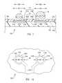
- FIG. 1is a cross-sectional view of a portion of a stackable variable height via package 100 during fabrication in accordance with one embodiment.
- FIG. 1Ais a top plan view of the portion of stackable variable height via package 100 of FIG. 1 .
- stackable variable height via package 100sometimes called an electronic component package, includes a substrate 102 including an upper, e.g., first, surface 102 U and an opposite lower, e.g., second, surface 102 L.
- substrate 102is a dielectric material such as laminate, ceramic, printed circuit board material, or other dielectric material.
- Terminals 104Formed on upper surface 102 U of substrate 102 are electrically conductive upper terminals 104 , e.g., formed of copper. Terminals 104 include a first terminal 104 A and a second terminal 104 B. Terminals 104 are electrically connected to electrically conductive upper, e.g., first, traces 106 on upper surface 102 U in one embodiment.
- terminals 104are essentially identical. More particularly, terminal 104 A and terminal 104 B have an equal width W 1 in the direction parallel to upper surface 102 U of substrate 102 . In one embodiment, terminal 104 A and terminal 104 B have an equal surface area when viewed from above, i.e., from a direction perpendicular to upper surface 102 U of substrate 102 , as illustrated in FIG. 1A .
- Stackable variable height via package 100further includes a solder mask 108 , i.e., formed of a dielectric material. Solder mask 108 is patterned to form terminal openings 110 above respective terminals 104 .
- terminal openings 110include a first terminal opening 110 A above terminal 104 A and a second terminal opening 110 B above terminal 104 B.
- Terminal openings 110have a width W 2 less than width W 1 of terminals 104 . Accordingly, an exposed portion 112 A of terminal 104 A is exposed through terminal opening 110 A and a covered portion 114 A of terminal 104 A is covered by solder mask 108 . Similarly, an exposed portion 112 B of terminal 104 B is exposed through terminal opening 110 B and a covered portion 114 B of terminal 104 B is covered by solder mask 108 . Exposed portions 112 A, 112 B and covered portions 114 A, 114 B are collectively referred to as exposed portions 112 and covered portions 114 of terminals 104 .
- exposed portions 112are the central regions of terminals 104 and covered portions 114 are the peripheral regions of terminals 104 .
- terminals 104 and terminal openings 110are circular when viewed from above as illustrated in FIG. 1A .
- terminals 104 and terminal openings 110have non circular shapes, e.g., are rectangular, square, oval or other shape.
- terminals 104have a diameter equal to width W 1 . Further, terminal openings 110 have a diameter equal to width W 2 .
- Terminals 104 and upper traces 106are illustrated in dashed lines in FIG. 1A as the structures are covered by solder mask 108 . Exposed portions 112 of terminals 104 are sometimes called Solder Mask Defined (SMD) lands 112 . SMD lands 112 are solder wettable in accordance with this embodiment. The terms “SMD lands 112 ” and “exposed portions 112 ” are used interchangeably herein.
- solder balls 116 , 118are attached to SMD lands 112 , e.g., using solder flux or other technique as those of skill in the art will understand in light of this disclosure. Solder balls 116 , 118 are not illustrated in the view of FIG. 1A for clarity of presentation.
- solder balls 116 , 118are formed of solder, i.e., are formed completely and only of solder. In another embodiment, solder balls 116 , 118 are polymer core solder balls, i.e., are formed of a polymer core surrounded by solder.
- Solder ball 116has a smaller volume than solder ball 118 in accordance with this embodiment. More particularly, solder balls 116 , 118 are approximate spherical. Solder ball 116 has a first diameter D 1 less than a second diameter D 2 of solder ball 118 .
- FIG. 2is a cross-sectional view of the portion of stackable variable height via package 100 of FIG. 1 at a later stage during fabrication in accordance with one embodiment.
- solder balls 116 , 118are ref lowed to form electrically conductive vias 220 , 222 , respectively.
- stackable variable height via package 100is heated to melt solder balls 116 , 118 which flow to cover SMD lands 112 . Recall that SMD lands 112 are solder wettable.
- Stackable variable height via package 100is cooled to solidify molten solder balls 116 , 118 thus forming vias 220 , 222 , respectively.
- solder ball 118 spread over SMD land 112 Bcauses via 222 to extend higher from upper surface 102 U than via 220 formed from solder ball 116 spread over SMD land 112 A. More particularly, via 220 has a height H 1 from upper surface 102 U of substrate 102 less than a height H 2 of via 222 from upper surface 102 U of substrate 102 .
- stackable variable height via package 100 with variable height viasi.e., vias 220 , 222
- vias 220 , 222readily accommodate stacking of additional packages having different types of terminals, e.g., land grid array (LGA) and ball grid array (BGA) type packages, as well as variable degrees of warpage on stackable variable height via package 100 .
- vias 220 , 222are formed with a minimum pitch.
- a package body 224e.g., molding compound, encapsulant, or other dielectric material, is applied to upper surface 102 U of substrate 102 .
- Package body 224covers solder mask 108 and vias 220 , 222 .
- Package body 224includes a principal surface 224 P parallel to upper surface 102 U of substrate 102 .
- via apertures 226are formed in package body 224 to expose respective vias 220 , 222 .
- via apertures 226are formed using a laser-ablation process. More particularly, a laser is repeatedly directed at principal surface 224 P perpendicularly to principal surface 224 P. This laser ablates, i.e., removes, portions of package body 224 leaving via apertures 226 , sometimes called through holes.
- via apertures 226are formed using selective molding, milling, mechanical drilling, chemical etching and/or other via aperture formation techniques.
- via apertures 226extend between principal surface 224 P of package body 224 and vias 220 , 222 . Accordingly, vias 220 , 222 are exposed through via aperture 226 .
- Via apertures 226taper from principal surface 124 P to vias 220 , 222 . More particularly, the diameter of via apertures 226 in a plane parallel to principal surface 224 P is greatest at the tops of via apertures 226 , and smallest at the bottoms of via apertures 226 and gradually diminishes between the tops and bottoms of via apertures 226 .
- the tops of via apertures 230are located at principal surface 224 P and the bottoms of via apertures 226 are located between principal surface 224 P of package body 224 and upper surface 102 U of substrate 102 , i.e., at vias 220 , 222 , in this embodiment.
- via apertures 226have a uniform diameter, i.e., have a cylindrical shape. In yet another embodiment, via apertures 226 taper from the bottoms to the tops of via aperture 226 . More particularly, the diameter of via apertures 226 in a plane parallel to principal surface 224 P is smallest at the tops of via apertures 226 and greatest at the bottoms of via apertures 226 and gradually increases between the tops and bottoms of via apertures 226 .
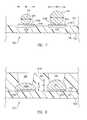
- FIG. 3is a cross-sectional view of a portion of a stackable variable height via package 300 during fabrication in accordance with another embodiment.
- Stackable variable height via package 300 of FIG. 3is similar to stackable variable height via package 100 of FIG. 1 and only the significant differences are discussed below.
- terminal openings 110 in solder mask 108are formed with various widths W 2 , W 3 . More particularly, terminal opening 110 A has width W 2 less than width W 1 of terminals 104 . Further, a terminal opening 110 C of terminal openings 110 has a width W 3 less than second width W 2 of terminal opening 110 A and also less than width W 1 of terminals 104 . Accordingly, exposed portion 112 C of terminal 104 B exposed through terminal opening 110 C is smaller, i.e., has a smaller surface area, than exposed portion 112 A of terminal 104 A. Exposed portions 112 A, 112 C are also referred to as SMD lands 112 A, 112 C, respectively.
- solder balls 116 A, 116 Bare attached to SMD lands 112 A, 112 C, i.e., exposed portions 112 A, 112 C of terminals 104 A, 104 B.
- solder balls 116 A, 116 Bhave equal volume and are essentially identical. More particularly, solder balls 116 A, 116 B are approximate spherical and have first diameter D 1 .
- FIG. 4is a cross-sectional view of the portion of stackable variable height via package 300 of FIG. 3 at a later stage during fabrication in accordance with one embodiment.
- solder balls 116 A, 116 Bare reflowed to form electrically conductive vias 220 , 422 on SMD lands 112 A, 112 C, respectively.
- solder ball 116 Ais spread over SMD land 112 A and solder ball 116 B is spread over SMD land 112 C.
- SMD land 112 Ahas a greater surface area than SMD land 112 C and solder balls 116 A, 116 B have an equal volume in accordance with this embodiment, via 422 extends higher from upper surface 102 U of substrate 102 than via 220 .
- via 220has height H 1 from upper surface 102 U of substrate 102 less than a height H 3 of via 422 from upper surface 102 U of substrate 102 .
- forming stackable variable height via package 300 with variable height viase.g., vias 220 , 422 , readily accommodates stacking of additional packages having different types of terminals, e.g., LGA and BGA type packages, as well as variable degrees of warpage on stackable variable height via package 300 .
- package body 224e.g., molding compound, encapsulant, or other dielectric material, is applied to upper surface 102 U of substrate 102 .
- Package body 224covers solder mask 108 and vias 220 , 422 .
- via apertures 226are formed in package body 224 to expose respective vias 220 , 422 .
- FIG. 5Ais a cross-sectional view of a portion of a stackable variable height via package 500 A during fabrication in accordance with another embodiment.
- Stackable variable height via package 500 A of FIG. 5Ais similar to stackable variable height via package 100 of FIG. 1 and only the significant differences are discussed below.
- terminal openings 110 in solder mask 108are formed with various widths W 4 , W 2 . More particularly, a terminal opening 110 D has a width W 4 greater than width W 1 of terminals 104 . Accordingly, terminal 104 A, including the upper, e.g., first, surface 104 U and sides 104 S of terminal 104 A, is entirely exposed through terminal opening 110 D. Thus, exposed portion 112 D of terminal 104 A is the entire terminal 104 A including upper surface 104 U and sides 104 S.
- terminal 104 Aincluding upper surface 104 U and sides 104 S defines the land.
- exposed portion 112 Dis upper surface 104 U and sides 104 S of terminal 104 A.
- exposed portion 112 Dis sometimes called a Non Solder Mask Defined (NSMD) land 112 D.
- exposed portion 112 B of terminal 104 B exposed through terminal opening 110 Bis smaller, i.e., has a smaller surface area, than exposed portion 112 D.
- solder balls 116 A, 116 Bare attached to NSMD land 112 D and SMD land 112 B.
- solder balls 116 A, 116 Bhave equal volume and are essentially identical. More particularly, solder balls 116 A, 116 B are approximate spherical and have first diameter D 1 .
- FIG. 6Ais a cross-sectional view of the portion of stackable variable height via package 500 A of FIG. 5A at a later stage during fabrication in accordance with one embodiment.
- solder balls 116 A, 116 Bare reflowed to form electrically conductive vias 620 A, 622 on NSMD land 112 D and SMD land 112 B, respectively.
- via 620 Aextends around and encloses both upper surface 104 U and sides 104 S of terminal 104 A.
- solder ball 116 Ais spread over NSMD land 112 D including upper surface 104 U and sides 104 S of terminal 104 A
- solder ball 116 Bis spread over SMD land 112 B.
- NSMD land 112 Dupper surface 104 U and sides 104 S combined
- solder balls 116 A, 116 Bhave equal volume in accordance with this embodiment
- via 622extends higher from upper surface 102 U than via 620 A.
- via 620 Ahas a height H 4 from upper surface 102 U of substrate 102 less than a height H 5 of via 622 from upper surface 102 U of substrate 102 .
- stackable variable height via package 500 A with variable height viase.g., vias 620 A, 622
- vias 620 A, 622readily accommodates stacking of additional packages having different types of terminals, e.g., LGA and BGA type packages, as well as variable degrees of warpage on stackable variable height via package 500 A.
- vias 620 A, 622are formed with minimum pitch.
- package body 224e.g., molding compound, encapsulant, or other dielectric material, is applied to upper surface 102 U of substrate 102 .
- Package body 224covers solder mask 108 , the exposed portion of upper surface 102 U, and vias 620 A, 622 .
- via apertures 226are formed in package body 224 to expose respective vias 620 A, 622 .
- FIG. 5Bis a cross-sectional view of a portion of a stackable variable height via package 500 B during fabrication in accordance with another embodiment.
- Stackable variable height via package 500 B of FIG. 5Bis similar to stackable variable height via package 500 A of FIG. 5A and only the significant differences are discussed below.
- terminal 104 Ahas width W 2 equal to width W 2 of terminal opening 110 B. More particularly, terminal opening 110 D has a width W 4 greater than width W 2 of terminal 104 A. Accordingly, terminal 104 A, including upper surface 104 U and sides 104 S of terminal 104 A, is entirely exposed through terminal opening 110 D. Thus, exposed portion 112 D of terminal 104 A is the entire terminal 104 A including upper surface 104 U and sides 104 S.
- terminal 104 Aincluding upper surface 104 U and sides 104 S defines the land.
- exposed portion 112 Dis upper surface 104 U and sides 104 S of terminal 104 A.
- exposed portion 112 Dis sometimes called a Non Solder Mask Defined (NSMD) land 112 D.
- upper surface 104 U of terminal 104 Ais equal to exposed portion 112 B of terminal 104 B.
- solder wettable area of NSMD land 112 Dis greater than the solder wettable area of SMD land 112 B.
- solder balls 116 A, 116 Bare attached to NSMD land 112 D and SMD land 112 B.
- solder balls 116 A, 116 Bhave equal volume and are essentially identical. More particularly, solder balls 116 A, 116 B are approximate spherical and have first diameter D 1 .
- FIG. 6Bis a cross-sectional view of the portion of stackable variable height via package 500 B of FIG. 5B at a later stage during fabrication in accordance with one embodiment.
- solder balls 116 A, 116 Bare ref lowed to form electrically conductive vias 620 B, 622 on NSMD land 112 D and SMD land 112 B, respectively.
- via 620 Bextends around and encloses both upper surface 104 U and sides 104 S of terminal 104 A.
- solder ball 116 Ais spread over NSMD land 112 D including upper surface 104 U and sides 104 S of terminal 104 A
- solder ball 116 Bis spread over SMD land 112 B.
- NSMD land 112 Dupper surface 104 U and sides 104 S combined
- solder balls 116 A, 116 Bhave equal volume in accordance with this embodiment
- via 622extends higher from upper surface 102 U than via 620 B.
- via 620 Bhas a height H 4 B from upper surface 102 U of substrate 102 less than a height H 5 of via 622 from upper surface 102 U of substrate 102 .
- stackable variable height via package 500 B with variable height viase.g., vias 620 B, 622
- vias 620 B, 622are formed with minimum pitch.
- package body 224e.g., molding compound, encapsulant, or other dielectric material, is applied to upper surface 102 U of substrate 102 .
- Package body 224covers solder mask 108 , the exposed portion of upper surface 102 U, and vias 620 B, 622 .
- via apertures 226are formed in package body 224 to expose respective vias 620 B, 622 .
- FIG. 7is a cross-sectional view of a portion of a stackable variable height via package 700 during fabrication in accordance with another embodiment.
- Stackable variable height via package 700 of FIG. 7is similar to stackable variable height via package 100 of FIG. 1 and only the significant differences are discussed below.
- stackable variable height via package 700is formed without solder mask 108 (see FIG. 1 ) or solder mask 108 is formed elsewhere on stackable variable height via package 700 . Accordingly, terminals 104 A, 104 B including upper surfaces 104 U and sides 104 S are both entirely exposed. Thus, exposed portions 112 D, 112 E of terminals 104 A, 104 B are the entire terminals 104 A, 104 B including upper surfaces 104 U and sides 104 S, respectively.
- terminals 104 A, 104 B including upper surfaces 104 U and sides 104 Sdefine the lands.
- exposed portions 112 D, 112 Eare upper surfaces 104 U and sides 104 S of terminals 104 A, 104 B.
- exposed portions 112 D, 112 Eare sometimes called Non Solder Mask Defined (NSMD) lands 112 D, 112 E, respectively. Both NSMD lands 112 D, 112 E have an equal width W 1 and thus have an equal surface area.
- NSMDNon Solder Mask Defined
- solder balls 116 , 118are attached to NSMD lands 112 D, 112 E.
- Solder ball 116has a smaller volume than solder ball 118 in accordance with this embodiment. More particularly, solder balls 116 , 118 are approximate spherical. Solder ball 116 has first diameter D 1 less than second diameter D 2 of solder ball 118 .
- FIG. 8is a cross-sectional view of the portion of stackable variable height via package 700 of FIG. 7 at a later stage during fabrication in accordance with one embodiment.
- solder balls 116 , 118are ref lowed to form electrically conductive vias 620 A, 822 , respectively.
- vias 620 A, 822extend around and enclose upper surfaces 104 U and sides 104 S of terminals 104 A, 104 B.
- the greater volume of solder ball 118 spread over NSMD land 112 Ecauses via 822 to extend higher from upper surface 102 U than via 620 A formed from solder ball 116 spread over NSMD land 112 D. More particularly, via 620 A has height H 4 from upper surface 102 U of substrate 102 less than a height H 6 of via 822 from upper surface 102 U of substrate 102 .
- stackable variable height via package 700 with variable height viase.g., vias 620 A, 822
- vias 620 A, 822readily accommodate stacking of additional packages having different types of terminals, e.g., LGA and BGA type packages, as well as variable degrees of warpage on stackable variable height via package 700 .
- vias 620 A, 822are formed with a minimum pitch.
- package body 224e.g., molding compound, encapsulant, or other dielectric material, is applied to upper surface 102 U of substrate 102 .
- Package body 224covers upper surface 102 U of substrate 102 and vias 620 A, 822 .
- via apertures 226are formed in package body 224 to expose respective vias 620 A, 822 .
- FIG. 9is a cross-sectional view of a portion of a stackable variable height via package 900 during fabrication in accordance with another embodiment.
- Stackable variable height via package 900 of FIG. 9is similar to stackable variable height via package 100 of FIG. 1 and only the significant differences are discussed below.
- stackable variable height via package 900is formed without solder mask 108 (see FIG. 1 ) or solder mask 108 is formed elsewhere on stackable variable height via package 900 . Accordingly, terminals 104 A, 104 C including upper surfaces 104 U and sides 104 S of terminals 104 A, 104 C are both entirely exposed. Thus, exposed portions 112 D, 112 F of terminals 104 A, 104 C are the entire terminals 104 A, 104 C including upper surfaces 104 U and sides 104 S, respectively.
- terminals 104 A, 104 C including upper surfaces 104 U and sides 104 Sdefine the lands.
- exposed portions 112 D, 112 Fare upper surfaces 104 U and sides 104 S of terminals 104 A, 104 C.
- exposed portions 112 D, 112 Fare sometimes called Non Solder Mask Defined (NSMD) lands 112 D, 112 F, respectively.
- NSMD lands 112 D, 112 Fare formed with various widths W 1 , W 5 . More particularly, NSMD land 112 F has width W 5 less than width W 1 of NSMD land 112 D. Accordingly, NSMD land 112 F is smaller, i.e., has a smaller surface area, than NSMD land 112 D.
- solder balls 116 A, 116 Bare attached to NSMD lands 112 D, 112 F, respectively.
- solder balls 116 A, 116 Bhave equal volume and are essentially identical. More particularly, solder balls 116 A, 116 B are approximate spherical and have first diameter D 1 .
- FIG. 10is a cross-sectional view of the portion of stackable variable height via package 900 of FIG. 9 at a later stage during fabrication in accordance with one embodiment.
- solder balls 116 A, 116 Bare reflowed to form electrically conductive vias 620 A, 1022 on NSMD lands 112 D, 112 F, respectively.
- vias 620 A, 1022extend around and enclose upper surfaces 104 U and sides 104 S of terminals 104 A, 104 C.
- solder ball 116 Ais spread over NSMD land 112 D and solder ball 116 B is spread over NSMD land 112 F.
- NSMD land 112 Dhas a greater surface area than NSMD land 112 F and solder balls 116 A, 116 B have equal volume in accordance with this embodiment
- via 1022extends higher from upper surface 102 U than via 620 A.
- via 620 Ahas height H 4 from upper surface 102 U of substrate 102 less than a height H 7 of via 1022 from upper surface 102 U of substrate 102 .
- stackable variable height via package 900 with variable height viase.g., vias 620 A, 1022
- variable height viase.g., vias 620 A, 1022
- additional packageshaving different types of terminals, e.g., LGA and BGA type packages, as well as variable degrees of warpage on stackable variable height via package 900 .
- package body 224e.g., molding compound, encapsulant, or other dielectric material, is applied to upper surface 102 U of substrate 102 .
- Package body 224covers upper surface 102 U of substrate 102 and vias 620 A, 1022 .
- via apertures 226are formed in package body 224 to expose respective vias 620 A, 1022 .
- FIG. 11is a cross-sectional view of a portion of a stackable variable height via package 1100 during fabrication in accordance with yet another embodiment.
- Stackable variable height via package 1100 of FIG. 11is similar to stackable variable height via package 100 of FIG. 2 and only the significant differences are discussed below.
- vias 220 , 220 A formed on SMD lands 112 A, 112 Bare identical and have a same height H 1 from upper surface 102 U of substrate 102 .
- two identical solder balls 116are reflowed to form vias 220 , 220 A on SMD lands 112 A, 112 B.
- a buildup solder ball 1128is placed into via aperture 226 and on via 220 A. Note a buildup solder ball is not placed in via aperture 226 and on via 220 . Although a buildup solder ball 1128 is illustrated and discussed herein, in other embodiments, solder paste is placed into via aperture 226 and on via 220 A.
- FIG. 12is a cross-sectional view of the portion of stackable variable height via package 1100 of FIG. 11 at a later stage during fabrication in accordance with one embodiment.
- stackable variable height via package 1100is heated to reflow via 220 A and buildup solder ball 1128 creating a protruding via 1230 . More particularly, via 220 A and buildup solder ball 1128 are heated to a melt, combine together into a single molten structure, and solidify upon cooling to form protruding via 1230 .
- Protruding via 1230extends higher from upper surface 102 U than via 220 . More particularly, protruding via 1230 has a height H 8 from upper surface 102 U of substrate 102 greater than height H 1 of via 220 from upper surface 102 U of substrate 102 . As discussed in greater detail below, forming stackable variable height via package 1100 with variable height vias, e.g., vias 220 , 1230 , readily accommodates stacking of additional packages having different types of terminals, e.g., LGA and BGA type packages, as well as variable degrees of warpage on stackable variable height via package 1100 . Further, vias 220 , 1230 are formed with a minimum pitch.
- height H 8 of protruding via 1230is also greater than a height H 9 of principal surface 224 P of package body 224 from upper surface 102 U of substrate 102 . Accordingly, protruding via 1230 protrudes outward beyond (above) principal surface 224 P of package body 224 . In contrast, height H 1 of via 220 is less than height H 9 of principal surface 224 P such that via 220 is recessed below principal surface 224 P.
- any of vias 220 , 222 ( FIG. 2 ), 422 ( FIG. 4 ), 620 A, 622 ( FIG. 6A ), 620 B ( FIG. 6B ), 822 ( FIG. 8 ), 1022 ( FIG. 10 )are built up by reflowing a buildup solder ball 1128 ( FIG. 11 ) to form a protruding via similar to protruding via 1230 .
- stackable variable height via packages 100 , 300 , 500 A, 500 B, 700 , 900 , 1100are discuss and illustrated as including vias 220 , 222 ( FIG. 2 ), 220 , 422 ( FIG. 4 ), 620 A, 622 ( FIG. 6A ), 620 B, 622 ( FIG. 6B ), 620 A, 822 ( FIG. 8 ), 620 A, 1022 ( FIG. 10 ), 220 , 1230 ( FIG.
- a stackable variable height via packagein accordance with various embodiments is fabricated with one or more of vias 220 , 222 , 422 , 620 A, 620 B, 622 , 822 , 1022 , 1230 , and/or combinations thereof.
- FIG. 13is a top plan view of a stackable variable height via package 1300 in accordance with another embodiment.
- FIG. 14is a cross-sectional view of stackable variable height via package 1300 of FIG. 13 along the line XIV-XIV in accordance with one embodiment.
- stackable variable height via package 1300includes an electronic component 1432 .
- electronic component 1432is an integrated circuit chip, e.g., an active component.
- electronic component 1432is a passive component such as a capacitor, resistor, or inductor.
- electronic component 1432includes an active surface 1434 and an opposite inactive surface 1436 .
- Electronic component 1432further includes bond pads 1438 formed on active surface 1434 .
- Inactive surface 1436is mounted to upper surface 102 U of substrate 102 with an adhesive 1440 , sometimes called a die attach adhesive.
- electronic component 1432is illustrated and described as being mounted to upper surface 102 U of substrate 102 in a wirebond configuration, in other embodiments, electronic component 1432 is mounted to upper surface 102 U of substrate 102 in a different configuration such as a flip chip configuration such as that illustrated in FIG. 19 . In another embodiment, a plurality of electronic components are mounted to upper surface 102 U of substrate 102 , e.g., in a stacked configuration, such as that illustrated in FIG. 20 .
- electrically conductive uppere.g., first, traces 106 , e.g., formed of copper.
- Bond pads 1438are electrically connected to upper traces 106 , e.g., bond fingers thereof, by electrically conductive bond wires 1442 .
- Lower traces 1444are electrically connected to upper traces 106 by electrically conductive substrate vias 1446 extending through substrate 102 between upper surface 102 U and lower surface 102 L.
- stackable variable height via package 1300further includes solder masks on upper and lower surface 102 U, 102 L that protect first portions of upper and lower traces 106 , 1444 while exposing second portions, e.g., terminals and/or bond fingers, of upper and lower traces 106 , 1444 .
- electrically conductive pathway between bond pads 1438 and interconnection balls 1450is described above, other electrically conductive pathways can be formed.
- contact metallizationscan be formed between the various electrical conductors.
- substrate 102is a multilayer substrate and a plurality of substrate vias and/or internal traces form the electrical interconnection between upper traces 106 and lower traces 1444 .
- one or more of upper traces 106is not electrically connected to lower traces 1444 , i.e., is electrically isolated from lower traces 1444 , and electrically connected to bond pads 1438 .
- a first upper trace 106 A of the plurality of upper traces 106is electrically isolated from lower traces 1444 and electrically connected to a respective bond pad 1438 .
- the respective bond pad 1438 electrically connected to upper trace 106 Ais also electrically isolated from lower traces 1444 .
- one or more of upper traces 106is electrically connected to both bond pads 1438 and to lower traces 1444 .
- upper trace 106 Ais electrically connected to lower traces 1444 by a substrate via 1446 A of the plurality of substrate vias 1446 .
- the respective bond pad 1438is electrically connected to upper trace 106 A and is also electrically connected to lower traces 1444 .
- Substrate via 1446 Ais indicated by dashed lines to signify that formation of substrate via 1446 A is optional. If substrate via 1446 A is not formed, upper trace 106 A is electrically isolated from lower traces 1444 . Conversely, if substrate via 1446 A is formed, upper trace 106 A is electrically connected to lower traces 1444 .
- one or more of upper traces 106is not electrically connected to a bond pad 1438 , i.e., is electrically isolated from bond pads 1438 , and is electrically connected to lower traces 1444 .
- the upper trace 106 to the far left of electronic component 1432 in the view of FIG. 14is electrically isolated from bond pads 1438 and electrically connected to lower traces 1444 .
- the respective lower traces 1444 electrically connected to the upper trace 106 electrically isolated from bond pads 1438are also electrically isolated from bond pads 1438 .
- connection between bond pads 1438 , upper traces 106 , and lower traces 1444are set forth above, in light of this disclosure, those of skill in the art will understand that any one of a number of electrical configurations are possible depending upon the particular application.
- Upper traces 106are electrically connected to terminals 104 on upper surface 102 U of substrate 102 .
- Variable height vias 220 , 222are formed on terminals 104 .
- stackable variable height via package 1300is discuss and illustrated as including vias 220 , 222 , in light of this disclosure, those of skill in the art will understand that a stackable variable height via package in accordance with various embodiments is fabricated with one or more of vias 220 , 222 , 422 , 620 A, 620 B, 622 , 822 , 1022 , 1230 , and/or combinations thereof as described above.
- upper traces 106are electrically connected to lower traces 1444 , to bond pads 1438 , and/or to lower traces 1444 and bond pads 1438 .
- vias 220 , 222are electrically connected to lower traces 1444 only, to bond pads 1438 only, and/or to both lower traces 1444 and bond pads 1438 .
- Package body 224is a cured liquid encapsulant, molding compound, or other dielectric material.
- Package body 224protects electronic component 1432 , bond wires 1442 , vias 220 , 222 , and the exposed portions of upper surface 102 U including upper traces 106 from the ambient environment, e.g., from contact, moisture and/or shorting to other structures.
- inactive surface 1436 of electronic component 1432is mounted to upper surface 102 U of substrate 102 by adhesive 1440 .
- Bond pads 1438are electrically connected to upper traces 106 by bond wires 1442 .
- Vias 220 , 222are formed on terminals 104 as described above.
- Electronic component 1432 , bond wires 1442 , vias 220 , 222 and the exposed portions of upper surface 102 U including upper traces 106are enclosed within package body 224 .
- Via apertures 226are formed in package body 224 to expose vias 220 , 222 as discussed above.
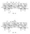
- FIG. 15is a cross-sectional view of an electronic component assembly 1500 including stackable variable height via package 1300 of FIG. 13 along the line XV-XV during fabrication in accordance with another embodiment.
- stackable variable height via package 1300includes protruding vias 1230 protruding above principal surface 224 P of package body 224 and vias 220 .
- Terminals 1552 of a Land Grid Array (LGA) electronic component package 1554are place on and in contact with protruding vias 1230 . Further, interconnection balls 1556 on terminals 1558 of Ball Grid Array (BGA) electronic component packages 1560 A, 1560 B are placed inside of via apertures 226 on and in contact with vias 220 .
- LGALand Grid Array
- BGABall Grid Array
- Electronic component assembly 1500is then heated to reflow vias 220 , 1230 and interconnection balls 1556 thus mounting LGA electronic component package 1554 and BGA electronic component packages 1560 A, 1560 B to stackable variable height via package 1300 as those of skill in the art will understand in light of this disclosure.
- variable height via package 1300 with variable height viase.g., vias 220 , 1230
- vias 220 , 1230readily accommodate stacking of additional packages 1554 , 1560 A, 1560 B having LGA and BGA types of terminals.
- vias 220 , 1230are formed with a minimum pitch.
- FIG. 16is a cross-sectional view of an electronic component assembly 1600 including stackable variable height via package 1300 of FIG. 13 along the line XV-XV during fabrication in accordance with another embodiment.
- stackable variable height via package 1300includes vias 220 , 222 in accordance with this embodiment.
- Electronic component assembly 1600further includes a warped Ball Grid Array (BGA) package 1662 containing an electronic component.
- Warped BGA package 1662is warped, i.e., is not completely planar.
- Warped BGA package 1662is sometimes called bent, curved, and/or non-planar. More particularly, warped BGA package 1662 is bent from a hypothetical plane 1664 indicated by the dashed line.
- Warped BGA package 1662includes interconnection balls 1666 on terminals 1668 on a terminal, e.g., first, surface 1670 of warped BGA package 1662 .
- Warped BGA package 1662further includes a second surface 1672 opposite terminal surface 1670 .
- warped BGA package 1662is bent in the concave direction relative to terminal surface 1670 . Stated another way, warped BGA package 1662 is concavely warped. Accordingly, the periphery P of terminal surface 1670 , and in particularly the corners, are bent inward (downward in the view of FIG. 16 ) relative to the center C of terminal surface 1670 . Thus, interconnection balls 1666 line upon a concave curve 1674 instead of lying upon a plane.
- Vias 220 , 222accommodate the curvature of interconnection ball 1666 thus insuring formation of reliable interconnections therewith.
- vias 220are formed adjacent to periphery P, and in particular, at the corners.
- vias 222which have a greater height than vias 220 , are formed adjacent to center C.
- vias 220 , 222i.e., two different height vias, are set forth, in light of this disclosure, those of skill in the art will understand that a plurality of different height vias are formed to accommodate the particular warpage of the package being mounted on stackable variable height via package 1300 in accordance with other embodiments.
- package body 224includes shortened corners 1676 .
- Shortened corners 1676are formed at the corners 1378 (see FIG. 13 ) of stackable variable height via package 1300 . Corners 1378 are defined at the intersections of sides 1380 of stackable variable height via package 1300 . Shortened corners 1676 are indicated by the dashed lines in FIG. 13 to indicate that shortened corners 1676 are optional.
- Shortened corners 1676have a height H 10 from upper surface 102 U of substrate 102 less than height H 9 of principal surface 224 P of package body 224 from upper surface 102 U of substrate 102 .
- shortened corners 1676are formed by removal of package body 224 at corners 1378 . In other embodiments, shortened corners 1676 are formed using selective molding, or other techniques.
- warped BGA package 1662By forming stackable variable height via package 1300 with shortened corners 1676 , clearance is provided for the corners of warped BGA package 1662 .
- the corners of warped BGA package 1662typically have the greatest inward offset (warpage) of warped BGA package 1662 . Accordingly, inadvertent and undesirable contact between the corners of warped BGA package 1662 and package body 224 is prevented thus insuring formation of reliable interconnections with warped BGA package 1662 .
- FIG. 17is a cross-sectional view of electronic component assembly 1600 of FIG. 16 at a later stage during fabrication in accordance with one embodiment.
- interconnection balls 1666are placed in contact with vias 220 , 222 as illustrated in FIG. 16 .
- Assembly 1600is heated to reflow interconnection balls 1666 and vias 220 , 222 forming solder columns 1780 as illustrated in FIG. 17 .
- interconnection balls 1666 and vias 220 , 222are heated to melt interconnection balls 1666 and vias 220 , 222 .
- interconnection balls 1666 and vias 220 , 222combine into a single molten structures, e.g., molten solder. These molten structures cool and form solder columns 1780 .
- solder columns 1780are integral, i.e., are single unitary structures and not a plurality of different layers connected together.
- Solder columns 1780physically and electrically connect terminals 104 of stackable variable height via package 1300 with terminals 1668 of warped BGA package 1662 .
- Solder columns 1780are formed with variable height to accommodate the warpage of warped BGA package 1662 . More particularly, solder columns 1780 A of the plurality of solder columns 1780 are formed adjacent to periphery P, and in particular, at the corners. In contrast, solder columns 1780 B of the plurality of solder columns 1780 , which have a greater height than solder columns 1780 A, are formed adjacent to center C.
- FIG. 18is a cross-sectional view of an electronic component assembly 1800 including stackable variable height via package 1300 of FIG. 13 along the line XV-XV during fabrication in accordance with another embodiment.
- stackable variable height via package 1300includes three different height vias 220 , 222 , 1881 in accordance with this embodiment.
- Height H 1 of vias 220is less than height H 11 of vias 1881 , which is less than height H 2 of vias 222 , from upper surface 102 U of substrate 102 .
- Vias 1881are formed using any one of the variable height via formation techniques discussed above in reference to FIGS. 1-12 .
- Electronic component assembly 1800further includes a warped Ball Grid Array (BGA) package 1882 .
- Warped BGA package 1882is warped, i.e., is not completely planar.
- Warped BGA package 1882is sometimes called bent, curved, and/or non-planar. More particularly, warped BGA package 1882 is bent from a hypothetical plane 1884 .
- Warped BGA package 1882includes interconnection balls 1886 on terminals 1888 on a terminal, e.g., first, surface 1890 of warped BGA package 1882 .
- Warped BGA package 1882further includes a second surface 1892 opposite terminal surface 1890 .
- warped BGA package 1882is bent in the convex direction relative to terminal surface 1890 . Stated another way, warped BGA package 1882 is convexly warped. Accordingly, the periphery P of terminal surface 1890 , and in particularly the corners, are bent outward (upward in the view of FIG. 18 ) relative to the center C of terminal surface 1890 . Thus, interconnection balls 1886 line upon a convex curve 1894 instead of line upon a plane.
- Vias 220 , 1881 , 222accommodate the curvature of interconnection ball 1886 thus insuring formation of reliable interconnections therewith.
- vias 222are formed adjacent to periphery P, and in particular, at the corners.
- vias 220which have a lesser height than vias 222 , are formed adjacent to center C.
- Vias 1881which have a height between vias 222 and vias 220 , are formed between vias 222 and vias 220 .
- vias 222are formed at the corners, vias 1881 are formed adjacent vias 222 only, and the remaining vias are vias 220 .
- vias 220 , 1881 , 222i.e., three different height vias, are set forth, in light of this disclosure, those of skill in the art will understand that a plurality of different height vias are formed to accommodate the particular warpage of the package being mounted on stackable variable height via package 1300 in accordance with other embodiments.
- interconnection balls 1886are placed inside of via apertures 226 on and in contact with vias 220 , 1881 , 222 .
- Assembly 1800is heated to reflow interconnection balls 1886 and vias 220 , 1881 , 222 forming solder columns in a manner similar to that illustrated in FIG. 17 , except that taller solder columns are formed adjacent periphery P of terminal surface 1890 , and in particularly the corners, relative to the solder columns formed at center C of terminal surface 1890 .
- FIG. 19is a cross-sectional view of a stackable variable height via package 1900 in accordance with another embodiment.
- Stackable variable height via package 1900 of FIG. 19is similar to stackable variable height via package 1300 of FIG. 14 and only the significant differences between stackable variable height via package 1900 and stackable variable height via package 1300 are discussed below.
- electronic component 1432is mounted in a flip chip configuration. More particularly, bond pads 1438 are electrically and physically connected to upper traces 106 , e.g., bond fingers thereof, by flip chip bumps 1996 , e.g., solder bumps.
- flip chip bumps 1996e.g., solder bumps.
- an underfill 1998is applied between upper surface 102 U of substrate 102 and active surface 1434 of electronic component 1432 and around flip chip bumps 1996 .
- FIG. 20is a cross-sectional view of a stackable variable height via package 2000 in accordance with yet another embodiment.
- Stackable variable height via package 2000 of FIG. 20is similar to stackable variable height via package 1300 of FIG. 14 and only the significant differences between stackable variable height via package 2000 and stackable variable height via package 1300 are discussed below.
- a second electronic component 2002is mounted to electronic component 1432 , sometimes called a first electronic component, in a stacked configuration.
- second electronic component 2002is an integrated circuit chip, e.g., an active component.
- second electronic component 2002is a passive component such as a capacitor, resistor, or inductor.
- second electronic component 2002includes an active surface 2004 and an opposite inactive surface 2006 .
- Second electronic component 2002further includes bond pads 2008 formed on active surface 2004 .
- Inactive surface 2006is mounted to active surface 1434 of first electronic component 1432 with an adhesive 2010 .
- Bond pads 2008are electrically connected to upper traces 106 , e.g., bond fingers thereof, by electrically conductive bond wires 2012 .
- Package body 224further encapsulates second electronic component 2002 including bond wires 2012 .
- FIG. 20Although one example of a stacked configuration is illustrated in FIG. 20 , in light of this disclosure, those of skill in the art will understand that other stacked configurations are used in other stackable variable height via packages in other embodiments.
Landscapes
- Engineering & Computer Science (AREA)
- Microelectronics & Electronic Packaging (AREA)
- Power Engineering (AREA)
- Physics & Mathematics (AREA)
- Condensed Matter Physics & Semiconductors (AREA)
- General Physics & Mathematics (AREA)
- Computer Hardware Design (AREA)
- Manufacturing & Machinery (AREA)
- Electric Connection Of Electric Components To Printed Circuits (AREA)
- Production Of Multi-Layered Print Wiring Board (AREA)
Abstract
Description
Claims (18)
Priority Applications (2)
| Application Number | Priority Date | Filing Date | Title |
|---|---|---|---|
| US12/537,048US8471154B1 (en) | 2009-08-06 | 2009-08-06 | Stackable variable height via package and method |
| US13/896,710US10257942B1 (en) | 2009-08-06 | 2013-05-17 | Stackable variable height via package and method |
Applications Claiming Priority (1)
| Application Number | Priority Date | Filing Date | Title |
|---|---|---|---|
| US12/537,048US8471154B1 (en) | 2009-08-06 | 2009-08-06 | Stackable variable height via package and method |
Related Child Applications (1)
| Application Number | Title | Priority Date | Filing Date |
|---|---|---|---|
| US13/896,710DivisionUS10257942B1 (en) | 2009-08-06 | 2013-05-17 | Stackable variable height via package and method |
Publications (1)
| Publication Number | Publication Date |
|---|---|
| US8471154B1true US8471154B1 (en) | 2013-06-25 |
Family
ID=48627654
Family Applications (2)
| Application Number | Title | Priority Date | Filing Date |
|---|---|---|---|
| US12/537,048Active2030-10-23US8471154B1 (en) | 2009-08-06 | 2009-08-06 | Stackable variable height via package and method |
| US13/896,710Active2032-07-29US10257942B1 (en) | 2009-08-06 | 2013-05-17 | Stackable variable height via package and method |
Family Applications After (1)
| Application Number | Title | Priority Date | Filing Date |
|---|---|---|---|
| US13/896,710Active2032-07-29US10257942B1 (en) | 2009-08-06 | 2013-05-17 | Stackable variable height via package and method |
Country Status (1)
| Country | Link |
|---|---|
| US (2) | US8471154B1 (en) |
Cited By (27)
| Publication number | Priority date | Publication date | Assignee | Title |
|---|---|---|---|---|
| US20090184412A1 (en)* | 2007-10-25 | 2009-07-23 | Rohm Co., Ltd. | Resin-seal type semiconductor device |
| US20120032340A1 (en)* | 2010-08-06 | 2012-02-09 | Stats Chippac, Ltd. | Semiconductor Die and Method of Forming FO-WLCSP Vertical Interconnect Using TSV and TMV |
| US20120228006A1 (en)* | 2011-03-10 | 2012-09-13 | Mediatek Inc. | Printed circuit board design for high speed application |
| US20130034956A1 (en)* | 2011-08-05 | 2013-02-07 | Taiwan Semiconductor Manufacturing Co., Ltd. | Cleaning residual molding compound on solder bumps |
| KR20130073757A (en)* | 2011-12-23 | 2013-07-03 | 엘지이노텍 주식회사 | Print circuit board substrate and method ofmanufacturing the same |
| US20140103527A1 (en)* | 2012-03-23 | 2014-04-17 | Stats Chippac, Ltd. | Semiconductor Device and Method of Forming a POP Device with Embedded Vertical Interconnect Units |
| US20140321089A1 (en)* | 2011-01-14 | 2014-10-30 | Harris Corporation | Method of making an electronic device having a liquid crystal polymer solder mask and related devices |
| US9391043B2 (en) | 2012-11-20 | 2016-07-12 | Amkor Technology, Inc. | Semiconductor device and manufacturing method thereof |
| US20160262258A1 (en)* | 2015-03-03 | 2016-09-08 | Nitto Denko Corporation | Wired circuit board |
| US20160276387A1 (en)* | 2013-09-05 | 2016-09-22 | Koninklijke Philips N.V. | Radiation detector element |
| US9543242B1 (en) | 2013-01-29 | 2017-01-10 | Amkor Technology, Inc. | Semiconductor package and fabricating method thereof |
| US9704842B2 (en) | 2013-11-04 | 2017-07-11 | Amkor Technology, Inc. | Interposer, manufacturing method thereof, semiconductor package using the same, and method for fabricating the semiconductor package |
| US9721872B1 (en)* | 2011-02-18 | 2017-08-01 | Amkor Technology, Inc. | Methods and structures for increasing the allowable die size in TMV packages |
| WO2017172135A1 (en)* | 2016-03-28 | 2017-10-05 | Intel Corporation | Variable ball height on ball grid array packages by solder paste transfer |
| US20170303396A1 (en)* | 2016-04-14 | 2017-10-19 | Ibiden Co., Ltd. | Printed wiring board and method for manufacturing the same |
| US9837303B2 (en) | 2012-03-23 | 2017-12-05 | STATS ChipPAC Pte. Ltd. | Semiconductor method and device of forming a fan-out device with PWB vertical interconnect units |
| US9865525B2 (en) | 2012-03-23 | 2018-01-09 | STATS ChipPAC Pte. Ltd. | Semiconductor method and device of forming a fan-out PoP device with PWB vertical interconnect units |
| US9960328B2 (en) | 2016-09-06 | 2018-05-01 | Amkor Technology, Inc. | Semiconductor device and manufacturing method thereof |
| US10049964B2 (en) | 2012-03-23 | 2018-08-14 | STATS ChipPAC Pte. Ltd. | Semiconductor device and method of forming a fan-out PoP device with PWB vertical interconnect units |
| US20190019775A1 (en)* | 2016-03-24 | 2019-01-17 | Toshiba Memory Corporation | Semiconductor device and method of manufacture thereof |
| US10304799B2 (en) | 2016-12-28 | 2019-05-28 | Intel Corporation | Land grid array package extension |
| US20190187389A1 (en)* | 2017-12-20 | 2019-06-20 | Shinko Electric Industries Co., Ltd. | Optical waveguide device and lens component |
| US10629476B2 (en)* | 2014-03-12 | 2020-04-21 | Taiwan Semiconductor Manufacturing Company, Ltd. | Packages with through-vias having tapered ends |
| US20230050785A1 (en)* | 2021-08-12 | 2023-02-16 | Taiwan Semiconductor Manufacturing Company, Ltd. | Semiconductor structure and manufacturing method thereof |
| US20230215797A1 (en)* | 2022-01-03 | 2023-07-06 | Mediatek Inc. | Board-level pad pattern for multi-row qfn packages |
| US12230557B2 (en) | 2021-05-14 | 2025-02-18 | Samsung Electronics Co., Ltd. | Semiconductor package |
| US12309921B2 (en) | 2022-01-03 | 2025-05-20 | Mediatek Inc. | Board-level pad pattern for multi-row QFN packages |
Families Citing this family (3)
| Publication number | Priority date | Publication date | Assignee | Title |
|---|---|---|---|---|
| TWI766283B (en)* | 2020-05-22 | 2022-06-01 | 南茂科技股份有限公司 | Semiconductor device |
| US11705378B2 (en)* | 2020-07-20 | 2023-07-18 | Taiwan Semiconductor Manufacturing Company, Ltd. | Semiconductor packages and methods of forming the same |
| US12027467B2 (en)* | 2021-01-29 | 2024-07-02 | Advanced Semiconductor Engineering, Inc. | Semiconductor device package and method of manufacturing the same |
Citations (164)
| Publication number | Priority date | Publication date | Assignee | Title |
|---|---|---|---|---|
| US3868724A (en) | 1973-11-21 | 1975-02-25 | Fairchild Camera Instr Co | Multi-layer connecting structures for packaging semiconductor devices mounted on a flexible carrier |
| US3916434A (en) | 1972-11-30 | 1975-10-28 | Power Hybrids Inc | Hermetically sealed encapsulation of semiconductor devices |
| US4322778A (en) | 1980-01-25 | 1982-03-30 | International Business Machines Corp. | High performance semiconductor package assembly |
| US4532419A (en) | 1982-09-09 | 1985-07-30 | Sony Corporation | Memory card having static electricity protection |
| US4642160A (en) | 1985-08-12 | 1987-02-10 | Interconnect Technology Inc. | Multilayer circuit board manufacturing |
| US4645552A (en) | 1984-11-19 | 1987-02-24 | Hughes Aircraft Company | Process for fabricating dimensionally stable interconnect boards |
| US4685033A (en) | 1984-08-28 | 1987-08-04 | Nec Corporation | Multilayer wiring substrate |
| US4706167A (en) | 1983-11-10 | 1987-11-10 | Telemark Co., Inc. | Circuit wiring disposed on solder mask coating |
| US4716049A (en) | 1985-12-20 | 1987-12-29 | Hughes Aircraft Company | Compressive pedestal for microminiature connections |
| US4786952A (en) | 1986-07-24 | 1988-11-22 | General Motors Corporation | High voltage depletion mode MOS power field effect transistor |
| US4806188A (en) | 1988-03-04 | 1989-02-21 | E. I. Du Pont De Nemours And Company | Method for fabricating multilayer circuits |
| US4811082A (en) | 1986-11-12 | 1989-03-07 | International Business Machines Corporation | High performance integrated circuit packaging structure |
| US4897338A (en) | 1987-08-03 | 1990-01-30 | Allied-Signal Inc. | Method for the manufacture of multilayer printed circuit boards |
| US4905124A (en) | 1987-03-31 | 1990-02-27 | Mitsubishi Denki Kabushiki Kaisha | IC card |
| US4964212A (en) | 1988-09-29 | 1990-10-23 | Commissariat A L'energie Atomique | Process for producing electrical connections through a substrate |
| US4974120A (en) | 1989-01-12 | 1990-11-27 | Mitsubishi Denki Kabushiki Kaisha | IC card |
| US4996391A (en) | 1988-09-30 | 1991-02-26 | Siemens Aktiengesellschaft | Printed circuit board having an injection molded substrate |
| US5021047A (en) | 1989-08-29 | 1991-06-04 | Movern John B | Restricted use hypodermic syringe |
| US5072075A (en) | 1989-06-28 | 1991-12-10 | Digital Equipment Corporation | Double-sided hybrid high density circuit board and method of making same |
| US5072520A (en) | 1990-10-23 | 1991-12-17 | Rogers Corporation | Method of manufacturing an interconnect device having coplanar contact bumps |
| US5081520A (en) | 1989-05-16 | 1992-01-14 | Minolta Camera Kabushiki Kaisha | Chip mounting substrate having an integral molded projection and conductive pattern |
| US5091769A (en) | 1991-03-27 | 1992-02-25 | Eichelberger Charles W | Configuration for testing and burn-in of integrated circuit chips |
| US5108553A (en) | 1989-04-04 | 1992-04-28 | Olin Corporation | G-tab manufacturing process and the product produced thereby |
| US5110664A (en) | 1989-07-10 | 1992-05-05 | Hitachi, Ltd. | Thick film and thin film composite substrate and electronic circuit apparatus using it |
| US5191174A (en) | 1990-08-01 | 1993-03-02 | International Business Machines Corporation | High density circuit board and method of making same |
| US5229550A (en) | 1990-10-30 | 1993-07-20 | International Business Machines Corporation | Encapsulated circuitized power core alignment and lamination |
| US5239448A (en) | 1991-10-28 | 1993-08-24 | International Business Machines Corporation | Formulation of multichip modules |
| US5247429A (en) | 1990-11-21 | 1993-09-21 | Nippondenso Co., Ltd. | Display board |
| US5250843A (en) | 1991-03-27 | 1993-10-05 | Integrated System Assemblies Corp. | Multichip integrated circuit modules |
| US5278726A (en) | 1992-01-22 | 1994-01-11 | Motorola, Inc. | Method and apparatus for partially overmolded integrated circuit package |
| US5283459A (en) | 1989-11-15 | 1994-02-01 | Kabushiki Kaisha Toshiba | Semiconductor sensor including an aperture having a funnel shaped section intersecting a second section |
| US5353498A (en) | 1993-02-08 | 1994-10-11 | General Electric Company | Method for fabricating an integrated circuit module |
| US5371654A (en) | 1992-10-19 | 1994-12-06 | International Business Machines Corporation | Three dimensional high performance interconnection package |
| US5379191A (en) | 1991-02-26 | 1995-01-03 | Microelectronics And Computer Technology Corporation | Compact adapter package providing peripheral to area translation for an integrated circuit chip |
| US5404044A (en) | 1992-09-29 | 1995-04-04 | International Business Machines Corporation | Parallel process interposer (PPI) |
| US5463253A (en) | 1990-03-15 | 1995-10-31 | Fujitsu Limited | Semiconductor device having a plurality of chips |
| US5474958A (en) | 1993-05-04 | 1995-12-12 | Motorola, Inc. | Method for making semiconductor device having no die supporting surface |
| US5474957A (en) | 1994-05-09 | 1995-12-12 | Nec Corporation | Process of mounting tape automated bonded semiconductor chip on printed circuit board through bumps |
| US5508938A (en) | 1992-08-13 | 1996-04-16 | Fujitsu Limited | Special interconnect layer employing offset trace layout for advanced multi-chip module packages |
| US5530288A (en) | 1994-10-12 | 1996-06-25 | International Business Machines Corporation | Passive interposer including at least one passive electronic component |
| US5531020A (en) | 1989-11-14 | 1996-07-02 | Poly Flex Circuits, Inc. | Method of making subsurface electronic circuits |
| US5546654A (en) | 1994-08-29 | 1996-08-20 | General Electric Company | Vacuum fixture and method for fabricating electronic assemblies |
| US5574309A (en) | 1991-11-25 | 1996-11-12 | Gemplus Card International | Integrated circuit card comprising means for the protection of the integrated circuit |
| US5581498A (en) | 1993-08-13 | 1996-12-03 | Irvine Sensors Corporation | Stack of IC chips in lieu of single IC chip |
| US5582858A (en) | 1991-10-07 | 1996-12-10 | International Business Machines Corporation | Adhesive layer in multi-level packaging and organic material as a metal diffusion barrier |
| US5616422A (en) | 1994-02-28 | 1997-04-01 | International Business Machines Corporation | Metallized substrate |
| US5637832A (en) | 1993-10-26 | 1997-06-10 | Pacific Microelectronics Corporation | Solder ball array and method of preparation |
| US5674785A (en) | 1995-11-27 | 1997-10-07 | Micron Technology, Inc. | Method of producing a single piece package for semiconductor die |
| US5719749A (en) | 1994-09-26 | 1998-02-17 | Sheldahl, Inc. | Printed circuit assembly with fine pitch flexible printed circuit overlay mounted to printed circuit board |
| US5726493A (en) | 1994-06-13 | 1998-03-10 | Fujitsu Limited | Semiconductor device and semiconductor device unit having ball-grid-array type package structure |
| US5739588A (en) | 1994-08-15 | 1998-04-14 | Citizen Watch Co., Ltd. | Semiconductor device |
| US5739581A (en) | 1995-11-17 | 1998-04-14 | National Semiconductor Corporation | High density integrated circuit package assembly with a heatsink between stacked dies |
| US5742479A (en) | 1994-03-09 | 1998-04-21 | Seiko Epson Corporation | Card-type electronic device with plastic frame sandwiched between printed circuit board and metal panel |
| US5774340A (en) | 1996-08-28 | 1998-06-30 | International Business Machines Corporation | Planar redistribution structure and printed wiring device |
| US5798014A (en) | 1995-02-02 | 1998-08-25 | Hestia Technologies, Inc. | Methods of making multi-tier laminate substrates for electronic device packaging |
| US5822190A (en) | 1996-06-11 | 1998-10-13 | Kabushiki Kaisha Toshiba | Card type memory device and a method for manufacturing the same |
| US5826330A (en) | 1995-12-28 | 1998-10-27 | Hitachi Aic Inc. | Method of manufacturing multilayer printed wiring board |
| US5835355A (en) | 1997-09-22 | 1998-11-10 | Lsi Logic Corporation | Tape ball grid array package with perforated metal stiffener |
| US5847453A (en) | 1996-03-27 | 1998-12-08 | Honda Giken Kogyo Kabushiki Kaisha | Microwave circuit package |
| US5883425A (en) | 1995-10-27 | 1999-03-16 | Mitsubishi Denki Kabushiki Kaisha | Circuit device |
| US5894108A (en) | 1997-02-11 | 1999-04-13 | National Semiconductor Corporation | Plastic package with exposed die |
| US5903052A (en) | 1998-05-12 | 1999-05-11 | Industrial Technology Research Institute | Structure for semiconductor package for improving the efficiency of spreading heat |
| US5907477A (en) | 1995-09-19 | 1999-05-25 | Micron Communications, Inc. | Substrate assembly including a compartmental dam for use in the manufacturing of an enclosed electrical circuit using an encapsulant |
| US5936843A (en) | 1997-10-14 | 1999-08-10 | Fujitsu Limited | Printed wiring board with mounted circuit element using a terminal density conversion board |
| US5952611A (en) | 1997-12-19 | 1999-09-14 | Texas Instruments Incorporated | Flexible pin location integrated circuit package |
| US6004619A (en) | 1996-11-07 | 1999-12-21 | Hewlett-Packard Company | Process for manufacturing printed circuit boards |
| US6013948A (en) | 1995-11-27 | 2000-01-11 | Micron Technology, Inc. | Stackable chip scale semiconductor package with mating contacts on opposed surfaces |
| US6021564A (en) | 1996-11-08 | 2000-02-08 | W. L. Gore & Associates, Inc. | Method for reducing via inductance in an electronic assembly and article |
| US6025648A (en)* | 1997-04-17 | 2000-02-15 | Nec Corporation | Shock resistant semiconductor device and method for producing same |
| US6028364A (en) | 1994-09-20 | 2000-02-22 | Hitachi, Ltd. | Semiconductor device having a stress relieving mechanism |
| US6034427A (en) | 1998-01-28 | 2000-03-07 | Prolinx Labs Corporation | Ball grid array structure and method for packaging an integrated circuit chip |
| US6035527A (en) | 1996-05-18 | 2000-03-14 | Ingenieurbuero Tamm Factory Innovations | Method for the production of printed circuit boards |
| US6040622A (en) | 1998-06-11 | 2000-03-21 | Sandisk Corporation | Semiconductor package using terminals formed on a conductive layer of a circuit board |
| US6060778A (en) | 1997-05-17 | 2000-05-09 | Hyundai Electronics Industries Co. Ltd. | Ball grid array package |
| US6069407A (en) | 1998-11-18 | 2000-05-30 | Vlsi Technology, Inc. | BGA package using PCB and tape in a die-up configuration |
| US6072243A (en) | 1996-11-26 | 2000-06-06 | Sharp Kabushiki Kaisha | Semiconductor integrated circuit device capable of surely electrically insulating two semiconductor chips from each other and fabricating method thereof |
| US6081036A (en) | 1996-04-19 | 2000-06-27 | Matsushita Electronics Corp. | Semiconductor device |
| US6122171A (en) | 1999-07-30 | 2000-09-19 | Micron Technology, Inc. | Heat sink chip package and method of making |
| US6119338A (en) | 1998-03-19 | 2000-09-19 | Industrial Technology Research Institute | Method for manufacturing high-density multilayer printed circuit boards |
| US6127833A (en) | 1999-01-04 | 2000-10-03 | Taiwan Semiconductor Manufacturing Co. | Test carrier for attaching a semiconductor device |
| US6160705A (en) | 1997-05-09 | 2000-12-12 | Texas Instruments Incorporated | Ball grid array package and method using enhanced power and ground distribution circuitry |
| US6172419B1 (en) | 1998-02-24 | 2001-01-09 | Micron Technology, Inc. | Low profile ball grid array package |
| US6175087B1 (en) | 1998-12-02 | 2001-01-16 | International Business Machines Corporation | Composite laminate circuit structure and method of forming the same |
| US6184463B1 (en) | 1998-04-13 | 2001-02-06 | Harris Corporation | Integrated circuit package for flip chip |
| US6194250B1 (en) | 1998-09-14 | 2001-02-27 | Motorola, Inc. | Low-profile microelectronic package |
| US6204453B1 (en) | 1998-12-02 | 2001-03-20 | International Business Machines Corporation | Two signal one power plane circuit board |
| US6214641B1 (en) | 1996-06-25 | 2001-04-10 | Micron Technology, Inc. | Method of fabricating a multi-chip module |
| US6239485B1 (en) | 1998-11-13 | 2001-05-29 | Fujitsu Limited | Reduced cross-talk noise high density signal interposer with power and ground wrap |
| USD445096S1 (en) | 1998-04-01 | 2001-07-17 | Sandisk Corporation | Removable memory card for use with portable electronic devices |
| USD446525S1 (en) | 1999-08-24 | 2001-08-14 | Kabushiki Kaisha Toshiba | IC memory card |
| US6274821B1 (en) | 1998-09-16 | 2001-08-14 | Denso Corporation | Shock-resistive printed circuit board and electronic device including the same |
| US6280641B1 (en) | 1998-06-02 | 2001-08-28 | Mitsubishi Gas Chemical Company, Inc. | Printed wiring board having highly reliably via hole and process for forming via hole |
| US6316285B1 (en) | 1998-09-02 | 2001-11-13 | Micron Technology, Inc. | Passivation layer for packaged integrated circuits |
| US20020017712A1 (en) | 1998-06-04 | 2002-02-14 | Yoshihiro Bessho | Method for fabricating a semiconductor package with a semiconductor device attached to a multilayered substrate |
| US6351031B1 (en) | 1999-10-12 | 2002-02-26 | Fujitsu Limited | Semiconductor device and method for manufacturing substrate of the same |
| US6353999B1 (en) | 1999-03-09 | 2002-03-12 | Unimicron Taiwan Corp. | Method of making mechanical-laser structure |
| US6365975B1 (en) | 1997-04-02 | 2002-04-02 | Tessera, Inc. | Chip with internal signal routing in external element |
| US6376906B1 (en) | 1997-02-12 | 2002-04-23 | Denso Corporation | Mounting structure of semiconductor element |
| US6392160B1 (en) | 1998-11-25 | 2002-05-21 | Lucent Technologies Inc. | Backplane for radio frequency signals |
| US20020061642A1 (en) | 1999-09-02 | 2002-05-23 | Matsushita Electric Industrial Co., Ltd. | Semiconductor device and method of manufacturing the same |
| US6395578B1 (en) | 1999-05-20 | 2002-05-28 | Amkor Technology, Inc. | Semiconductor package and method for fabricating the same |
| US20020066952A1 (en) | 2000-12-04 | 2002-06-06 | Fujitsu Limited | Semiconductor device having an interconnecting post formed on an interposer within a sealing resin |
| US6406942B2 (en) | 2000-03-09 | 2002-06-18 | Nec Corporation | Flip chip type semiconductor device and method for manufacturing the same |
| US6407930B1 (en) | 1999-06-23 | 2002-06-18 | Asustek Computer Inc. | Structure of printed circuit board with stacked daughter board |
| US6407341B1 (en) | 2000-04-25 | 2002-06-18 | International Business Machines Corporation | Conductive substructures of a multilayered laminate |
| US6405431B1 (en) | 1996-06-27 | 2002-06-18 | Samsung Electro-Mechanics Co., Ltd. | Method for manufacturing build-up multi-layer printed circuit board by using yag laser |
| US6448510B1 (en) | 1997-05-20 | 2002-09-10 | Micro Components Ltd. | Substrate for electronic packaging, pin jig fixture |
| US6479762B2 (en) | 2000-11-20 | 2002-11-12 | Alps Electric Co., Ltd. | Printed circuit board having a pattern of traces formed by screen-printing |
| US6497943B1 (en) | 2000-02-14 | 2002-12-24 | International Business Machines Corporation | Surface metal balancing to reduce chip carrier flexing |
| US20020195697A1 (en) | 2001-06-21 | 2002-12-26 | Mess Leonard E. | Stacked mass storage flash memory package |
| US20030025199A1 (en) | 2001-08-01 | 2003-02-06 | Chi-Chuan Wu | Super low profile package with stacked dies |
| US6517995B1 (en) | 1999-09-14 | 2003-02-11 | Massachusetts Institute Of Technology | Fabrication of finely featured devices by liquid embossing |
| US6534391B1 (en) | 2001-08-17 | 2003-03-18 | Amkor Technology, Inc. | Semiconductor package having substrate with laser-formed aperture through solder mask layer |
| US6544638B2 (en) | 1996-11-08 | 2003-04-08 | Gore Enterprise Holdings, Inc. | Electronic chip package |
| US6586682B2 (en) | 2000-02-23 | 2003-07-01 | Kulicke & Soffa Holdings, Inc. | Printed wiring board with controlled line impedance |
| US20030128096A1 (en) | 2002-01-10 | 2003-07-10 | Joseph Mazzochette | Temperature compensating device with integral sheet thermistors |
| US20030141582A1 (en) | 2002-01-25 | 2003-07-31 | Yang Chaur-Chin | Stack type flip-chip package |
| US6608757B1 (en) | 2002-03-18 | 2003-08-19 | International Business Machines Corporation | Method for making a printed wiring board |
| US20030197284A1 (en) | 2002-02-21 | 2003-10-23 | United Test & Assembly Center Limited | Semiconductor package |
| US6660559B1 (en) | 2001-06-25 | 2003-12-09 | Amkor Technology, Inc. | Method of making a chip carrier package using laser ablation |
| US20040063246A1 (en) | 2002-09-17 | 2004-04-01 | Chippac, Inc. | Semiconductor multi-package module having package stacked over die-down flip chip ball grid array package and having wire bond interconnect between stacked packages |
| US6715204B1 (en) | 1998-07-08 | 2004-04-06 | Ibiden Co., Ltd. | Printed wiring board and method for producing the same |
| US6727645B2 (en) | 2002-05-24 | 2004-04-27 | International Business Machines Corporation | Organic LED device |
| US6730857B2 (en) | 2001-03-13 | 2004-05-04 | International Business Machines Corporation | Structure having laser ablated features and method of fabricating |
| US6734542B2 (en) | 2000-12-27 | 2004-05-11 | Matsushita Electric Industrial Co., Ltd. | Component built-in module and method for producing the same |
| US6740964B2 (en) | 2000-11-17 | 2004-05-25 | Oki Electric Industry Co., Ltd. | Semiconductor package for three-dimensional mounting, fabrication method thereof, and semiconductor device |
| US6753612B2 (en) | 2001-04-05 | 2004-06-22 | International Business Machines Corporation | Economical high density chip carrier |
| US20040145044A1 (en) | 2002-01-23 | 2004-07-29 | Matsushita Electric Industrial Co., Ltd. | Circuit component built-in module with embedded semiconductor chip and method of manufacturing |
| US6774748B1 (en) | 1999-11-15 | 2004-08-10 | Nec Corporation | RF package with multi-layer substrate having coplanar feed through and connection interface |
| US20040159462A1 (en) | 1999-06-01 | 2004-08-19 | Chung Kevin Kwong-Tai | Flexible dielectric electronic substrate and method for making same |
| US6787443B1 (en) | 2003-05-20 | 2004-09-07 | Intel Corporation | PCB design and method for providing vented blind vias |
| US6803528B1 (en) | 1999-11-05 | 2004-10-12 | 3M Innovative Properties Company | Multi-layer double-sided wiring board and method of fabricating the same |
| US6815739B2 (en) | 2001-05-18 | 2004-11-09 | Corporation For National Research Initiatives | Radio frequency microelectromechanical systems (MEMS) devices on low-temperature co-fired ceramic (LTCC) substrates |
| US6815709B2 (en) | 2001-05-23 | 2004-11-09 | International Business Machines Corporation | Structure having flush circuitry features and method of making |
| US6828665B2 (en)* | 2002-10-18 | 2004-12-07 | Siliconware Precision Industries Co., Ltd. | Module device of stacked semiconductor packages and method for fabricating the same |
| US6838776B2 (en) | 2003-04-18 | 2005-01-04 | Freescale Semiconductor, Inc. | Circuit device with at least partial packaging and method for forming |
| US6888240B2 (en) | 2001-04-30 | 2005-05-03 | Intel Corporation | High performance, low cost microelectronic circuit package with interposer |
| US20050139985A1 (en) | 2003-12-25 | 2005-06-30 | Norio Takahashi | Semiconductor chip package and multichip package |
| US6921975B2 (en) | 2003-04-18 | 2005-07-26 | Freescale Semiconductor, Inc. | Circuit device with at least partial packaging, exposed active surface and a voltage reference plane |
| US6921968B2 (en) | 2003-05-02 | 2005-07-26 | Advance Semiconductor Engineering, Inc. | Stacked flip chip package |
| US6931726B2 (en) | 2001-10-16 | 2005-08-23 | International Business Machines Corporation | Method of making and interconnect structure |
| US6953995B2 (en) | 1996-03-12 | 2005-10-11 | Micron Technology, Inc. | Hermetic chip in wafer form |
| US20050242425A1 (en) | 2004-04-30 | 2005-11-03 | Leal George R | Semiconductor device with a protected active die region and method therefor |
| US7015075B2 (en) | 2004-02-09 | 2006-03-21 | Freescale Semiconuctor, Inc. | Die encapsulation using a porous carrier |
| US7030469B2 (en) | 2003-09-25 | 2006-04-18 | Freescale Semiconductor, Inc. | Method of forming a semiconductor package and structure thereof |
| US7081661B2 (en) | 2001-03-16 | 2006-07-25 | Matsushita Electric Industrial Co., Ltd. | High-frequency module and method for manufacturing the same |
| US7091619B2 (en)* | 2003-03-24 | 2006-08-15 | Seiko Epson Corporation | Semiconductor device, semiconductor package, electronic device, electronic apparatus, and manufacturing methods of semiconductor device and electronic device |
| US7185426B1 (en) | 2002-05-01 | 2007-03-06 | Amkor Technology, Inc. | Method of manufacturing a semiconductor package |
| US7198980B2 (en) | 2002-06-27 | 2007-04-03 | Micron Technology, Inc. | Methods for assembling multiple semiconductor devices |
| US7242081B1 (en) | 2006-04-24 | 2007-07-10 | Advanced Semiconductor Engineering Inc. | Stacked package structure |
| US7282394B2 (en) | 2004-12-30 | 2007-10-16 | Samsung Electro-Mechanics Co., Ltd. | Printed circuit board including embedded chips and method of fabricating the same using plating |
| US7285855B2 (en) | 2004-10-23 | 2007-10-23 | Freescale Semiconductor, Inc | Packaged device and method of forming same |
| US20070273049A1 (en) | 2006-05-12 | 2007-11-29 | Broadcom Corporation | Interconnect structure and formation for package stacking of molded plastic area array package |
| US20070281471A1 (en) | 2006-06-01 | 2007-12-06 | Dror Hurwitz | Advanced Multilayered Coreless Support Structures and their Fabrication |
| US20070290376A1 (en) | 2006-06-20 | 2007-12-20 | Broadcom Corporation | Integrated circuit (IC) package stacking and IC packages formed by same |
| US7345361B2 (en) | 2003-12-04 | 2008-03-18 | Intel Corporation | Stackable integrated circuit packaging |
| US7372151B1 (en) | 2003-09-12 | 2008-05-13 | Asat Ltd. | Ball grid array package and process for manufacturing same |
| US20080230887A1 (en)* | 2007-03-23 | 2008-09-25 | Advanced Semiconductor Engineering, Inc. | Semiconductor package and the method of making the same |
| US7429786B2 (en) | 2005-04-29 | 2008-09-30 | Stats Chippac Ltd. | Semiconductor package including second substrate and having exposed substrate surfaces on upper and lower sides |
| US7459202B2 (en) | 2006-07-03 | 2008-12-02 | Motorola, Inc. | Printed circuit board |
| US7548430B1 (en) | 2002-05-01 | 2009-06-16 | Amkor Technology, Inc. | Buildup dielectric and metallization process and semiconductor package |
| US7550857B1 (en) | 2006-11-16 | 2009-06-23 | Amkor Technology, Inc. | Stacked redistribution layer (RDL) die assembly package |
| US20100072600A1 (en)* | 2008-09-22 | 2010-03-25 | Texas Instrument Incorporated | Fine-pitch oblong solder connections for stacking multi-chip packages |
| US7994643B2 (en)* | 2007-04-04 | 2011-08-09 | Samsung Electronics Co., Ltd. | Stack package, a method of manufacturing the stack package, and a digital device having the stack package |
Family Cites Families (13)
| Publication number | Priority date | Publication date | Assignee | Title |
|---|---|---|---|---|
| JPH05109975A (en) | 1991-10-14 | 1993-04-30 | Hitachi Ltd | Resin-sealed type semiconductor device |
| JPH05136323A (en) | 1991-11-13 | 1993-06-01 | Nec Corp | Integrated circuit device |
| JPH0717175A (en) | 1993-06-22 | 1995-01-20 | Seiko Epson Corp | memory card |
| JPH08190615A (en) | 1995-01-09 | 1996-07-23 | Seiko Epson Corp | memory card |
| JPH10334205A (en) | 1997-05-30 | 1998-12-18 | Toshiba Corp | IC card and memory package |
| TW434856B (en)* | 2000-05-15 | 2001-05-16 | Siliconware Precision Industries Co Ltd | Manufacturing method for high coplanarity solder ball array of ball grid array integrated circuit package |
| US7633765B1 (en) | 2004-03-23 | 2009-12-15 | Amkor Technology, Inc. | Semiconductor package including a top-surface metal layer for implementing circuit features |
| US6987314B1 (en)* | 2004-06-08 | 2006-01-17 | Amkor Technology, Inc. | Stackable semiconductor package with solder on pads on which second semiconductor package is stacked |
| EP1887845A4 (en)* | 2005-06-30 | 2010-08-11 | Ibiden Co Ltd | Printed wiring board |
| US7312529B2 (en)* | 2005-07-05 | 2007-12-25 | International Business Machines Corporation | Structure and method for producing multiple size interconnections |
| US7777351B1 (en) | 2007-10-01 | 2010-08-17 | Amkor Technology, Inc. | Thin stacked interposer package |
| US7960827B1 (en) | 2009-04-09 | 2011-06-14 | Amkor Technology, Inc. | Thermal via heat spreader package and method |
| US8222538B1 (en)* | 2009-06-12 | 2012-07-17 | Amkor Technology, Inc. | Stackable via package and method |
- 2009
- 2009-08-06USUS12/537,048patent/US8471154B1/enactiveActive
- 2013
- 2013-05-17USUS13/896,710patent/US10257942B1/enactiveActive
Patent Citations (171)
| Publication number | Priority date | Publication date | Assignee | Title |
|---|---|---|---|---|
| US3916434A (en) | 1972-11-30 | 1975-10-28 | Power Hybrids Inc | Hermetically sealed encapsulation of semiconductor devices |
| US3868724A (en) | 1973-11-21 | 1975-02-25 | Fairchild Camera Instr Co | Multi-layer connecting structures for packaging semiconductor devices mounted on a flexible carrier |
| US4322778A (en) | 1980-01-25 | 1982-03-30 | International Business Machines Corp. | High performance semiconductor package assembly |
| US4532419A (en) | 1982-09-09 | 1985-07-30 | Sony Corporation | Memory card having static electricity protection |
| US4706167A (en) | 1983-11-10 | 1987-11-10 | Telemark Co., Inc. | Circuit wiring disposed on solder mask coating |
| US4685033A (en) | 1984-08-28 | 1987-08-04 | Nec Corporation | Multilayer wiring substrate |
| US4645552A (en) | 1984-11-19 | 1987-02-24 | Hughes Aircraft Company | Process for fabricating dimensionally stable interconnect boards |
| US4642160A (en) | 1985-08-12 | 1987-02-10 | Interconnect Technology Inc. | Multilayer circuit board manufacturing |
| US4716049A (en) | 1985-12-20 | 1987-12-29 | Hughes Aircraft Company | Compressive pedestal for microminiature connections |
| US4786952A (en) | 1986-07-24 | 1988-11-22 | General Motors Corporation | High voltage depletion mode MOS power field effect transistor |
| US4811082A (en) | 1986-11-12 | 1989-03-07 | International Business Machines Corporation | High performance integrated circuit packaging structure |
| US4905124A (en) | 1987-03-31 | 1990-02-27 | Mitsubishi Denki Kabushiki Kaisha | IC card |
| US4897338A (en) | 1987-08-03 | 1990-01-30 | Allied-Signal Inc. | Method for the manufacture of multilayer printed circuit boards |
| US4806188A (en) | 1988-03-04 | 1989-02-21 | E. I. Du Pont De Nemours And Company | Method for fabricating multilayer circuits |
| US4964212A (en) | 1988-09-29 | 1990-10-23 | Commissariat A L'energie Atomique | Process for producing electrical connections through a substrate |
| US4996391A (en) | 1988-09-30 | 1991-02-26 | Siemens Aktiengesellschaft | Printed circuit board having an injection molded substrate |
| US4974120A (en) | 1989-01-12 | 1990-11-27 | Mitsubishi Denki Kabushiki Kaisha | IC card |
| US5108553A (en) | 1989-04-04 | 1992-04-28 | Olin Corporation | G-tab manufacturing process and the product produced thereby |
| US5081520A (en) | 1989-05-16 | 1992-01-14 | Minolta Camera Kabushiki Kaisha | Chip mounting substrate having an integral molded projection and conductive pattern |
| US5072075A (en) | 1989-06-28 | 1991-12-10 | Digital Equipment Corporation | Double-sided hybrid high density circuit board and method of making same |
| US5110664A (en) | 1989-07-10 | 1992-05-05 | Hitachi, Ltd. | Thick film and thin film composite substrate and electronic circuit apparatus using it |
| US5021047A (en) | 1989-08-29 | 1991-06-04 | Movern John B | Restricted use hypodermic syringe |
| US5531020A (en) | 1989-11-14 | 1996-07-02 | Poly Flex Circuits, Inc. | Method of making subsurface electronic circuits |
| US5283459A (en) | 1989-11-15 | 1994-02-01 | Kabushiki Kaisha Toshiba | Semiconductor sensor including an aperture having a funnel shaped section intersecting a second section |
| US5463253A (en) | 1990-03-15 | 1995-10-31 | Fujitsu Limited | Semiconductor device having a plurality of chips |
| US5191174A (en) | 1990-08-01 | 1993-03-02 | International Business Machines Corporation | High density circuit board and method of making same |
| US5072520A (en) | 1990-10-23 | 1991-12-17 | Rogers Corporation | Method of manufacturing an interconnect device having coplanar contact bumps |
| US5229550A (en) | 1990-10-30 | 1993-07-20 | International Business Machines Corporation | Encapsulated circuitized power core alignment and lamination |
| US5247429A (en) | 1990-11-21 | 1993-09-21 | Nippondenso Co., Ltd. | Display board |
| US5379191A (en) | 1991-02-26 | 1995-01-03 | Microelectronics And Computer Technology Corporation | Compact adapter package providing peripheral to area translation for an integrated circuit chip |
| US5250843A (en) | 1991-03-27 | 1993-10-05 | Integrated System Assemblies Corp. | Multichip integrated circuit modules |
| US5091769A (en) | 1991-03-27 | 1992-02-25 | Eichelberger Charles W | Configuration for testing and burn-in of integrated circuit chips |
| US5582858A (en) | 1991-10-07 | 1996-12-10 | International Business Machines Corporation | Adhesive layer in multi-level packaging and organic material as a metal diffusion barrier |
| US5239448A (en) | 1991-10-28 | 1993-08-24 | International Business Machines Corporation | Formulation of multichip modules |
| US5574309A (en) | 1991-11-25 | 1996-11-12 | Gemplus Card International | Integrated circuit card comprising means for the protection of the integrated circuit |
| US5278726A (en) | 1992-01-22 | 1994-01-11 | Motorola, Inc. | Method and apparatus for partially overmolded integrated circuit package |
| US5508938A (en) | 1992-08-13 | 1996-04-16 | Fujitsu Limited | Special interconnect layer employing offset trace layout for advanced multi-chip module packages |
| US5404044A (en) | 1992-09-29 | 1995-04-04 | International Business Machines Corporation | Parallel process interposer (PPI) |
| US5371654A (en) | 1992-10-19 | 1994-12-06 | International Business Machines Corporation | Three dimensional high performance interconnection package |
| US5497033A (en) | 1993-02-08 | 1996-03-05 | Martin Marietta Corporation | Embedded substrate for integrated circuit modules |
| US5353498A (en) | 1993-02-08 | 1994-10-11 | General Electric Company | Method for fabricating an integrated circuit module |
| US5474958A (en) | 1993-05-04 | 1995-12-12 | Motorola, Inc. | Method for making semiconductor device having no die supporting surface |
| US5581498A (en) | 1993-08-13 | 1996-12-03 | Irvine Sensors Corporation | Stack of IC chips in lieu of single IC chip |
| US5637832A (en) | 1993-10-26 | 1997-06-10 | Pacific Microelectronics Corporation | Solder ball array and method of preparation |
| US5616422A (en) | 1994-02-28 | 1997-04-01 | International Business Machines Corporation | Metallized substrate |
| US5784259A (en) | 1994-03-09 | 1998-07-21 | Seiko Epson Corporation | Card-type electronic device with plastic frame sandwiched between printed circuit boarding metal panel |
| US5742479A (en) | 1994-03-09 | 1998-04-21 | Seiko Epson Corporation | Card-type electronic device with plastic frame sandwiched between printed circuit board and metal panel |
| US5474957A (en) | 1994-05-09 | 1995-12-12 | Nec Corporation | Process of mounting tape automated bonded semiconductor chip on printed circuit board through bumps |
| US5726493A (en) | 1994-06-13 | 1998-03-10 | Fujitsu Limited | Semiconductor device and semiconductor device unit having ball-grid-array type package structure |
| US5739588A (en) | 1994-08-15 | 1998-04-14 | Citizen Watch Co., Ltd. | Semiconductor device |
| US5546654A (en) | 1994-08-29 | 1996-08-20 | General Electric Company | Vacuum fixture and method for fabricating electronic assemblies |
| US6028364A (en) | 1994-09-20 | 2000-02-22 | Hitachi, Ltd. | Semiconductor device having a stress relieving mechanism |
| US5719749A (en) | 1994-09-26 | 1998-02-17 | Sheldahl, Inc. | Printed circuit assembly with fine pitch flexible printed circuit overlay mounted to printed circuit board |
| US5530288A (en) | 1994-10-12 | 1996-06-25 | International Business Machines Corporation | Passive interposer including at least one passive electronic component |
| US5798014A (en) | 1995-02-02 | 1998-08-25 | Hestia Technologies, Inc. | Methods of making multi-tier laminate substrates for electronic device packaging |
| US5907477A (en) | 1995-09-19 | 1999-05-25 | Micron Communications, Inc. | Substrate assembly including a compartmental dam for use in the manufacturing of an enclosed electrical circuit using an encapsulant |
| US5883425A (en) | 1995-10-27 | 1999-03-16 | Mitsubishi Denki Kabushiki Kaisha | Circuit device |
| US5739581A (en) | 1995-11-17 | 1998-04-14 | National Semiconductor Corporation | High density integrated circuit package assembly with a heatsink between stacked dies |
| US6235554B1 (en) | 1995-11-27 | 2001-05-22 | Micron Technology, Inc. | Method for fabricating stackable chip scale semiconductor package |
| US5739585A (en) | 1995-11-27 | 1998-04-14 | Micron Technology, Inc. | Single piece package for semiconductor die |
| US5674785A (en) | 1995-11-27 | 1997-10-07 | Micron Technology, Inc. | Method of producing a single piece package for semiconductor die |
| US6013948A (en) | 1995-11-27 | 2000-01-11 | Micron Technology, Inc. | Stackable chip scale semiconductor package with mating contacts on opposed surfaces |
| US5826330A (en) | 1995-12-28 | 1998-10-27 | Hitachi Aic Inc. | Method of manufacturing multilayer printed wiring board |
| US6953995B2 (en) | 1996-03-12 | 2005-10-11 | Micron Technology, Inc. | Hermetic chip in wafer form |
| US5847453A (en) | 1996-03-27 | 1998-12-08 | Honda Giken Kogyo Kabushiki Kaisha | Microwave circuit package |
| US6081036A (en) | 1996-04-19 | 2000-06-27 | Matsushita Electronics Corp. | Semiconductor device |
| US6035527A (en) | 1996-05-18 | 2000-03-14 | Ingenieurbuero Tamm Factory Innovations | Method for the production of printed circuit boards |
| US5822190A (en) | 1996-06-11 | 1998-10-13 | Kabushiki Kaisha Toshiba | Card type memory device and a method for manufacturing the same |
| US6214641B1 (en) | 1996-06-25 | 2001-04-10 | Micron Technology, Inc. | Method of fabricating a multi-chip module |
| US6405431B1 (en) | 1996-06-27 | 2002-06-18 | Samsung Electro-Mechanics Co., Ltd. | Method for manufacturing build-up multi-layer printed circuit board by using yag laser |
| US5774340A (en) | 1996-08-28 | 1998-06-30 | International Business Machines Corporation | Planar redistribution structure and printed wiring device |
| US6004619A (en) | 1996-11-07 | 1999-12-21 | Hewlett-Packard Company | Process for manufacturing printed circuit boards |
| US6021564A (en) | 1996-11-08 | 2000-02-08 | W. L. Gore & Associates, Inc. | Method for reducing via inductance in an electronic assembly and article |
| US6544638B2 (en) | 1996-11-08 | 2003-04-08 | Gore Enterprise Holdings, Inc. | Electronic chip package |
| US6072243A (en) | 1996-11-26 | 2000-06-06 | Sharp Kabushiki Kaisha | Semiconductor integrated circuit device capable of surely electrically insulating two semiconductor chips from each other and fabricating method thereof |
| US5894108A (en) | 1997-02-11 | 1999-04-13 | National Semiconductor Corporation | Plastic package with exposed die |
| US6376906B1 (en) | 1997-02-12 | 2002-04-23 | Denso Corporation | Mounting structure of semiconductor element |
| US6365975B1 (en) | 1997-04-02 | 2002-04-02 | Tessera, Inc. | Chip with internal signal routing in external element |
| US6025648A (en)* | 1997-04-17 | 2000-02-15 | Nec Corporation | Shock resistant semiconductor device and method for producing same |
| US6160705A (en) | 1997-05-09 | 2000-12-12 | Texas Instruments Incorporated | Ball grid array package and method using enhanced power and ground distribution circuitry |
| US6060778A (en) | 1997-05-17 | 2000-05-09 | Hyundai Electronics Industries Co. Ltd. | Ball grid array package |
| US6448510B1 (en) | 1997-05-20 | 2002-09-10 | Micro Components Ltd. | Substrate for electronic packaging, pin jig fixture |
| US5835355A (en) | 1997-09-22 | 1998-11-10 | Lsi Logic Corporation | Tape ball grid array package with perforated metal stiffener |
| US5936843A (en) | 1997-10-14 | 1999-08-10 | Fujitsu Limited | Printed wiring board with mounted circuit element using a terminal density conversion board |
| US5952611A (en) | 1997-12-19 | 1999-09-14 | Texas Instruments Incorporated | Flexible pin location integrated circuit package |
| US6034427A (en) | 1998-01-28 | 2000-03-07 | Prolinx Labs Corporation | Ball grid array structure and method for packaging an integrated circuit chip |
| US6172419B1 (en) | 1998-02-24 | 2001-01-09 | Micron Technology, Inc. | Low profile ball grid array package |
| US6119338A (en) | 1998-03-19 | 2000-09-19 | Industrial Technology Research Institute | Method for manufacturing high-density multilayer printed circuit boards |
| USD445096S1 (en) | 1998-04-01 | 2001-07-17 | Sandisk Corporation | Removable memory card for use with portable electronic devices |
| US6184463B1 (en) | 1998-04-13 | 2001-02-06 | Harris Corporation | Integrated circuit package for flip chip |
| US5903052A (en) | 1998-05-12 | 1999-05-11 | Industrial Technology Research Institute | Structure for semiconductor package for improving the efficiency of spreading heat |
| US6280641B1 (en) | 1998-06-02 | 2001-08-28 | Mitsubishi Gas Chemical Company, Inc. | Printed wiring board having highly reliably via hole and process for forming via hole |
| US20020017712A1 (en) | 1998-06-04 | 2002-02-14 | Yoshihiro Bessho | Method for fabricating a semiconductor package with a semiconductor device attached to a multilayered substrate |
| US6040622A (en) | 1998-06-11 | 2000-03-21 | Sandisk Corporation | Semiconductor package using terminals formed on a conductive layer of a circuit board |
| US6715204B1 (en) | 1998-07-08 | 2004-04-06 | Ibiden Co., Ltd. | Printed wiring board and method for producing the same |
| US6316285B1 (en) | 1998-09-02 | 2001-11-13 | Micron Technology, Inc. | Passivation layer for packaged integrated circuits |
| US6194250B1 (en) | 1998-09-14 | 2001-02-27 | Motorola, Inc. | Low-profile microelectronic package |
| US6274821B1 (en) | 1998-09-16 | 2001-08-14 | Denso Corporation | Shock-resistive printed circuit board and electronic device including the same |
| US6239485B1 (en) | 1998-11-13 | 2001-05-29 | Fujitsu Limited | Reduced cross-talk noise high density signal interposer with power and ground wrap |
| US6069407A (en) | 1998-11-18 | 2000-05-30 | Vlsi Technology, Inc. | BGA package using PCB and tape in a die-up configuration |
| US6392160B1 (en) | 1998-11-25 | 2002-05-21 | Lucent Technologies Inc. | Backplane for radio frequency signals |
| US6175087B1 (en) | 1998-12-02 | 2001-01-16 | International Business Machines Corporation | Composite laminate circuit structure and method of forming the same |
| US6204453B1 (en) | 1998-12-02 | 2001-03-20 | International Business Machines Corporation | Two signal one power plane circuit board |
| US6451509B2 (en) | 1998-12-02 | 2002-09-17 | International Business Machines Corporation | Composite laminate circuit structure and method of forming the same |
| US6127833A (en) | 1999-01-04 | 2000-10-03 | Taiwan Semiconductor Manufacturing Co. | Test carrier for attaching a semiconductor device |
| US6353999B1 (en) | 1999-03-09 | 2002-03-12 | Unimicron Taiwan Corp. | Method of making mechanical-laser structure |
| US6395578B1 (en) | 1999-05-20 | 2002-05-28 | Amkor Technology, Inc. | Semiconductor package and method for fabricating the same |
| US20040159462A1 (en) | 1999-06-01 | 2004-08-19 | Chung Kevin Kwong-Tai | Flexible dielectric electronic substrate and method for making same |
| US6407930B1 (en) | 1999-06-23 | 2002-06-18 | Asustek Computer Inc. | Structure of printed circuit board with stacked daughter board |
| US6122171A (en) | 1999-07-30 | 2000-09-19 | Micron Technology, Inc. | Heat sink chip package and method of making |
| USD446525S1 (en) | 1999-08-24 | 2001-08-14 | Kabushiki Kaisha Toshiba | IC memory card |
| US20020061642A1 (en) | 1999-09-02 | 2002-05-23 | Matsushita Electric Industrial Co., Ltd. | Semiconductor device and method of manufacturing the same |
| US6517995B1 (en) | 1999-09-14 | 2003-02-11 | Massachusetts Institute Of Technology | Fabrication of finely featured devices by liquid embossing |
| US6351031B1 (en) | 1999-10-12 | 2002-02-26 | Fujitsu Limited | Semiconductor device and method for manufacturing substrate of the same |
| US6803528B1 (en) | 1999-11-05 | 2004-10-12 | 3M Innovative Properties Company | Multi-layer double-sided wiring board and method of fabricating the same |
| US6774748B1 (en) | 1999-11-15 | 2004-08-10 | Nec Corporation | RF package with multi-layer substrate having coplanar feed through and connection interface |
| US6497943B1 (en) | 2000-02-14 | 2002-12-24 | International Business Machines Corporation | Surface metal balancing to reduce chip carrier flexing |
| US6586682B2 (en) | 2000-02-23 | 2003-07-01 | Kulicke & Soffa Holdings, Inc. | Printed wiring board with controlled line impedance |
| US6406942B2 (en) | 2000-03-09 | 2002-06-18 | Nec Corporation | Flip chip type semiconductor device and method for manufacturing the same |
| US6407341B1 (en) | 2000-04-25 | 2002-06-18 | International Business Machines Corporation | Conductive substructures of a multilayered laminate |
| US6740964B2 (en) | 2000-11-17 | 2004-05-25 | Oki Electric Industry Co., Ltd. | Semiconductor package for three-dimensional mounting, fabrication method thereof, and semiconductor device |
| US6479762B2 (en) | 2000-11-20 | 2002-11-12 | Alps Electric Co., Ltd. | Printed circuit board having a pattern of traces formed by screen-printing |
| US20020066952A1 (en) | 2000-12-04 | 2002-06-06 | Fujitsu Limited | Semiconductor device having an interconnecting post formed on an interposer within a sealing resin |
| US6734542B2 (en) | 2000-12-27 | 2004-05-11 | Matsushita Electric Industrial Co., Ltd. | Component built-in module and method for producing the same |
| US6919514B2 (en) | 2001-03-13 | 2005-07-19 | International Business Machines Corporation | Structure having laser ablated features and method of fabricating |
| US6730857B2 (en) | 2001-03-13 | 2004-05-04 | International Business Machines Corporation | Structure having laser ablated features and method of fabricating |
| US7081661B2 (en) | 2001-03-16 | 2006-07-25 | Matsushita Electric Industrial Co., Ltd. | High-frequency module and method for manufacturing the same |
| US7125744B2 (en) | 2001-03-16 | 2006-10-24 | Matsushita Electric Industrial Co., Ltd. | High-frequency module and method for manufacturing the same |
| US6753612B2 (en) | 2001-04-05 | 2004-06-22 | International Business Machines Corporation | Economical high density chip carrier |
| US6888240B2 (en) | 2001-04-30 | 2005-05-03 | Intel Corporation | High performance, low cost microelectronic circuit package with interposer |
| US6815739B2 (en) | 2001-05-18 | 2004-11-09 | Corporation For National Research Initiatives | Radio frequency microelectromechanical systems (MEMS) devices on low-temperature co-fired ceramic (LTCC) substrates |
| US6815709B2 (en) | 2001-05-23 | 2004-11-09 | International Business Machines Corporation | Structure having flush circuitry features and method of making |
| US20020195697A1 (en) | 2001-06-21 | 2002-12-26 | Mess Leonard E. | Stacked mass storage flash memory package |
| US6660559B1 (en) | 2001-06-25 | 2003-12-09 | Amkor Technology, Inc. | Method of making a chip carrier package using laser ablation |
| US20030025199A1 (en) | 2001-08-01 | 2003-02-06 | Chi-Chuan Wu | Super low profile package with stacked dies |
| US6534391B1 (en) | 2001-08-17 | 2003-03-18 | Amkor Technology, Inc. | Semiconductor package having substrate with laser-formed aperture through solder mask layer |
| US6931726B2 (en) | 2001-10-16 | 2005-08-23 | International Business Machines Corporation | Method of making and interconnect structure |
| US20030128096A1 (en) | 2002-01-10 | 2003-07-10 | Joseph Mazzochette | Temperature compensating device with integral sheet thermistors |
| US20040145044A1 (en) | 2002-01-23 | 2004-07-29 | Matsushita Electric Industrial Co., Ltd. | Circuit component built-in module with embedded semiconductor chip and method of manufacturing |
| US20030141582A1 (en) | 2002-01-25 | 2003-07-31 | Yang Chaur-Chin | Stack type flip-chip package |
| US20030197284A1 (en) | 2002-02-21 | 2003-10-23 | United Test & Assembly Center Limited | Semiconductor package |
| US6608757B1 (en) | 2002-03-18 | 2003-08-19 | International Business Machines Corporation | Method for making a printed wiring board |
| US7548430B1 (en) | 2002-05-01 | 2009-06-16 | Amkor Technology, Inc. | Buildup dielectric and metallization process and semiconductor package |
| US7185426B1 (en) | 2002-05-01 | 2007-03-06 | Amkor Technology, Inc. | Method of manufacturing a semiconductor package |
| US6727645B2 (en) | 2002-05-24 | 2004-04-27 | International Business Machines Corporation | Organic LED device |
| US7198980B2 (en) | 2002-06-27 | 2007-04-03 | Micron Technology, Inc. | Methods for assembling multiple semiconductor devices |
| US20040063246A1 (en) | 2002-09-17 | 2004-04-01 | Chippac, Inc. | Semiconductor multi-package module having package stacked over die-down flip chip ball grid array package and having wire bond interconnect between stacked packages |
| US6828665B2 (en)* | 2002-10-18 | 2004-12-07 | Siliconware Precision Industries Co., Ltd. | Module device of stacked semiconductor packages and method for fabricating the same |
| US7091619B2 (en)* | 2003-03-24 | 2006-08-15 | Seiko Epson Corporation | Semiconductor device, semiconductor package, electronic device, electronic apparatus, and manufacturing methods of semiconductor device and electronic device |
| US6838776B2 (en) | 2003-04-18 | 2005-01-04 | Freescale Semiconductor, Inc. | Circuit device with at least partial packaging and method for forming |
| US6921975B2 (en) | 2003-04-18 | 2005-07-26 | Freescale Semiconductor, Inc. | Circuit device with at least partial packaging, exposed active surface and a voltage reference plane |
| US6921968B2 (en) | 2003-05-02 | 2005-07-26 | Advance Semiconductor Engineering, Inc. | Stacked flip chip package |
| US6787443B1 (en) | 2003-05-20 | 2004-09-07 | Intel Corporation | PCB design and method for providing vented blind vias |
| US7372151B1 (en) | 2003-09-12 | 2008-05-13 | Asat Ltd. | Ball grid array package and process for manufacturing same |
| US7030469B2 (en) | 2003-09-25 | 2006-04-18 | Freescale Semiconductor, Inc. | Method of forming a semiconductor package and structure thereof |
| US7345361B2 (en) | 2003-12-04 | 2008-03-18 | Intel Corporation | Stackable integrated circuit packaging |
| US20050139985A1 (en) | 2003-12-25 | 2005-06-30 | Norio Takahashi | Semiconductor chip package and multichip package |
| US7015075B2 (en) | 2004-02-09 | 2006-03-21 | Freescale Semiconuctor, Inc. | Die encapsulation using a porous carrier |
| US20050242425A1 (en) | 2004-04-30 | 2005-11-03 | Leal George R | Semiconductor device with a protected active die region and method therefor |
| US7285855B2 (en) | 2004-10-23 | 2007-10-23 | Freescale Semiconductor, Inc | Packaged device and method of forming same |
| US7282394B2 (en) | 2004-12-30 | 2007-10-16 | Samsung Electro-Mechanics Co., Ltd. | Printed circuit board including embedded chips and method of fabricating the same using plating |
| US7429786B2 (en) | 2005-04-29 | 2008-09-30 | Stats Chippac Ltd. | Semiconductor package including second substrate and having exposed substrate surfaces on upper and lower sides |
| US7242081B1 (en) | 2006-04-24 | 2007-07-10 | Advanced Semiconductor Engineering Inc. | Stacked package structure |
| US20070273049A1 (en) | 2006-05-12 | 2007-11-29 | Broadcom Corporation | Interconnect structure and formation for package stacking of molded plastic area array package |
| US20070281471A1 (en) | 2006-06-01 | 2007-12-06 | Dror Hurwitz | Advanced Multilayered Coreless Support Structures and their Fabrication |
| US20070290376A1 (en) | 2006-06-20 | 2007-12-20 | Broadcom Corporation | Integrated circuit (IC) package stacking and IC packages formed by same |
| US7459202B2 (en) | 2006-07-03 | 2008-12-02 | Motorola, Inc. | Printed circuit board |
| US7550857B1 (en) | 2006-11-16 | 2009-06-23 | Amkor Technology, Inc. | Stacked redistribution layer (RDL) die assembly package |
| US20080230887A1 (en)* | 2007-03-23 | 2008-09-25 | Advanced Semiconductor Engineering, Inc. | Semiconductor package and the method of making the same |
| US7994643B2 (en)* | 2007-04-04 | 2011-08-09 | Samsung Electronics Co., Ltd. | Stack package, a method of manufacturing the stack package, and a digital device having the stack package |
| US20100072600A1 (en)* | 2008-09-22 | 2010-03-25 | Texas Instrument Incorporated | Fine-pitch oblong solder connections for stacking multi-chip packages |
Non-Patent Citations (11)
| Title |
|---|
| Berry et al., "Thin Stacked Interposer Package", U.S. Appl. No. 11/865,617, filed Oct. 1, 2007. |
| Hiner et al., "Printed Wiring Motherboard Having Bonded Interconnect Redistribution Mesa", U.S. Appl. No. 10/992,371, filed Nov. 18, 2004. |
| Hiner et al., "Semiconductor Package Including Top-Surface Terminals for Mounting Another Semiconductor Package", U.S. Appl. No. 11/595,411, filed Nov. 9, 2006. |
| Huemoeller et al., "Build Up Motherboard Fabrication Method and Structure", U.S. Appl. No. 11/824,395, filed Jun. 29, 2007. |
| Huemoeller et al., "Buildup Dielectric Layer Having Metallization Pattern Semiconductor Package Fabrication Method", U.S. Appl. No. 12/387,691, filed May 5, 2009. |
| IBM Technical Disclosure Bulletin, "Microstructure Solder Mask by Means of a Laser", vol. 36, Issue 11, p. 589, Nov. 1, 1993. |
| Kim et al., "Application of Through Mold Via (TMV) as PoP base package", 58th ECTC Proceedings, May 2008, Lake Buena Vista, FL, 6 pages, IEEE. |
| Longo et al., "Stacked Redistribution Layer (RDL) Die Assembly Package", U.S. Appl. No. 12/387,672, filed May 5, 2009. |
| Miller, Jr. et al., "Thermal Via Heat Spreader Package and Method", U.S. Appl. No. 12/421,118, filed Apr. 9, 2009. |
| Scanlan et al., "Semiconductor Package Including a Top-Surface Metal Layer for Implementing Circuit Features", U.S. Appl. No. 11/293,999, filed Dec. 5, 2005. |
| Scanlan, "Package-on-package (PoP) with Through-mold Vias", Advanced Packaging, Jan. 2008, 3 pages, vol. 17, Issue 1, PennWell Corporation. |
Cited By (70)
| Publication number | Priority date | Publication date | Assignee | Title |
|---|---|---|---|---|
| US20090184412A1 (en)* | 2007-10-25 | 2009-07-23 | Rohm Co., Ltd. | Resin-seal type semiconductor device |
| US9484282B2 (en)* | 2007-10-25 | 2016-11-01 | Rohm Co., Ltd. | Resin-sealed semiconductor device |
| US9153494B2 (en) | 2010-08-06 | 2015-10-06 | Stats Chippac, Ltd. | Semiconductor die and method of forming Fo-WLCSP vertical interconnect using TSV and TMV |
| US20120032340A1 (en)* | 2010-08-06 | 2012-02-09 | Stats Chippac, Ltd. | Semiconductor Die and Method of Forming FO-WLCSP Vertical Interconnect Using TSV and TMV |
| US8895440B2 (en)* | 2010-08-06 | 2014-11-25 | Stats Chippac, Ltd. | Semiconductor die and method of forming Fo-WLCSP vertical interconnect using TSV and TMV |
| US20170339785A1 (en)* | 2011-01-14 | 2017-11-23 | Harris Corporation | Method of making an electronic device having a liquid crystal polymer solder mask and related devices |
| US9763324B2 (en)* | 2011-01-14 | 2017-09-12 | Harris Corporation | Method of making an electronic device having a liquid crystal polymer solder mask and related devices |
| US10342126B2 (en)* | 2011-01-14 | 2019-07-02 | Harris Corporation | Electronic device having a liquid crystal polymer solder mask and related devices |
| US20140321089A1 (en)* | 2011-01-14 | 2014-10-30 | Harris Corporation | Method of making an electronic device having a liquid crystal polymer solder mask and related devices |
| US9721872B1 (en)* | 2011-02-18 | 2017-08-01 | Amkor Technology, Inc. | Methods and structures for increasing the allowable die size in TMV packages |
| US10347562B1 (en) | 2011-02-18 | 2019-07-09 | Amkor Technology, Inc. | Methods and structures for increasing the allowable die size in TMV packages |
| US11488892B2 (en) | 2011-02-18 | 2022-11-01 | Amkor Technology Singapore Holding Pte. Ltd. | Methods and structures for increasing the allowable die size in TMV packages |
| US20120228006A1 (en)* | 2011-03-10 | 2012-09-13 | Mediatek Inc. | Printed circuit board design for high speed application |
| US9949360B2 (en)* | 2011-03-10 | 2018-04-17 | Mediatek Inc. | Printed circuit board design for high speed application |
| US8748306B2 (en)* | 2011-08-05 | 2014-06-10 | Taiwan Semiconductor Manufacturing Co., Ltd. | Cleaning residual molding compound on solder bumps |
| US20130034956A1 (en)* | 2011-08-05 | 2013-02-07 | Taiwan Semiconductor Manufacturing Co., Ltd. | Cleaning residual molding compound on solder bumps |
| KR20130073757A (en)* | 2011-12-23 | 2013-07-03 | 엘지이노텍 주식회사 | Print circuit board substrate and method ofmanufacturing the same |
| US20160295684A1 (en)* | 2011-12-23 | 2016-10-06 | Lg Innotek Co., Ltd. | Printed circuit board and method of fabricating the same |
| US9814129B2 (en)* | 2011-12-23 | 2017-11-07 | Lg Innotek Co., Ltd. | Printed circuit board and method of fabricating the same |
| US9842798B2 (en)* | 2012-03-23 | 2017-12-12 | STATS ChipPAC Pte. Ltd. | Semiconductor device and method of forming a PoP device with embedded vertical interconnect units |
| US10446479B2 (en) | 2012-03-23 | 2019-10-15 | STATS ChipPAC Pte. Ltd. | Semiconductor device and method of forming a PoP device with embedded vertical interconnect units |
| US10049964B2 (en) | 2012-03-23 | 2018-08-14 | STATS ChipPAC Pte. Ltd. | Semiconductor device and method of forming a fan-out PoP device with PWB vertical interconnect units |
| US11024561B2 (en) | 2012-03-23 | 2021-06-01 | STATS ChipPAC Pte. Ltd. | Semiconductor device and method of forming a fan-out PoP device with PWB vertical interconnect units |
| US10707150B2 (en) | 2012-03-23 | 2020-07-07 | STATS ChipPAC Pte. Ltd. | Semiconductor device and method of forming a fan-out PoP device with PWB vertical interconnect units |
| US20140103527A1 (en)* | 2012-03-23 | 2014-04-17 | Stats Chippac, Ltd. | Semiconductor Device and Method of Forming a POP Device with Embedded Vertical Interconnect Units |
| US9865525B2 (en) | 2012-03-23 | 2018-01-09 | STATS ChipPAC Pte. Ltd. | Semiconductor method and device of forming a fan-out PoP device with PWB vertical interconnect units |
| US9837303B2 (en) | 2012-03-23 | 2017-12-05 | STATS ChipPAC Pte. Ltd. | Semiconductor method and device of forming a fan-out device with PWB vertical interconnect units |
| US10679952B2 (en) | 2012-11-20 | 2020-06-09 | Amkor Technology, Inc. | Semiconductor device having an encapsulated front side and interposer and manufacturing method thereof |
| US9391043B2 (en) | 2012-11-20 | 2016-07-12 | Amkor Technology, Inc. | Semiconductor device and manufacturing method thereof |
| US9728514B2 (en) | 2012-11-20 | 2017-08-08 | Amkor Technology, Inc. | Semiconductor device and manufacturing method thereof |
| US11527496B2 (en) | 2012-11-20 | 2022-12-13 | Amkor Technology Singapore Holding Pte. Ltd. | Semiconductor device comprising semiconductor die and interposer and manufacturing method thereof |
| US9852976B2 (en) | 2013-01-29 | 2017-12-26 | Amkor Technology, Inc. | Semiconductor package and fabricating method thereof |
| US9543242B1 (en) | 2013-01-29 | 2017-01-10 | Amkor Technology, Inc. | Semiconductor package and fabricating method thereof |
| US9748300B2 (en)* | 2013-09-05 | 2017-08-29 | Koninklijke Philips N.V. | Radiation detector element |
| US20160276387A1 (en)* | 2013-09-05 | 2016-09-22 | Koninklijke Philips N.V. | Radiation detector element |
| US9704842B2 (en) | 2013-11-04 | 2017-07-11 | Amkor Technology, Inc. | Interposer, manufacturing method thereof, semiconductor package using the same, and method for fabricating the semiconductor package |
| US10192816B2 (en) | 2013-11-19 | 2019-01-29 | Amkor Technology, Inc. | Semiconductor package and fabricating method thereof |
| US10943858B2 (en) | 2013-11-19 | 2021-03-09 | Amkor Technology Singapore Holding Pte. Ltd. | Semiconductor package and fabricating method thereof |
| US12159823B2 (en) | 2013-11-19 | 2024-12-03 | Amkor Technology Singapore Holding Pte. Ltd. | Semiconductor package with front side and back side redistribution structures and fabricating method thereof |
| US11652038B2 (en) | 2013-11-19 | 2023-05-16 | Amkor Technology Singapore Holding Pte. Ltd. | Semiconductor package with front side and back side redistribution structures and fabricating method thereof |
| US11043410B2 (en) | 2014-03-12 | 2021-06-22 | Taiwan Semiconductor Manufacturing Company, Ltd. | Packages with through-vias having tapered ends |
| US10629476B2 (en)* | 2014-03-12 | 2020-04-21 | Taiwan Semiconductor Manufacturing Company, Ltd. | Packages with through-vias having tapered ends |
| US20160262258A1 (en)* | 2015-03-03 | 2016-09-08 | Nitto Denko Corporation | Wired circuit board |
| US9713245B2 (en)* | 2015-03-03 | 2017-07-18 | Nitto Denko Corporation | Wired circuit board |
| US20190019775A1 (en)* | 2016-03-24 | 2019-01-17 | Toshiba Memory Corporation | Semiconductor device and method of manufacture thereof |
| US10256205B2 (en) | 2016-03-28 | 2019-04-09 | Intel Corporation | Variable ball height on ball grid array packages by solder paste transfer |
| US10504863B2 (en) | 2016-03-28 | 2019-12-10 | Intel Corporation | Variable ball height on ball grid array packages by solder paste transfer |
| US9842818B2 (en) | 2016-03-28 | 2017-12-12 | Intel Corporation | Variable ball height on ball grid array packages by solder paste transfer |
| US20190096838A1 (en)* | 2016-03-28 | 2019-03-28 | Intel Corporation | Variable ball height on ball grid array packages by solder paste transfer |
| TWI713690B (en)* | 2016-03-28 | 2020-12-21 | 美商英特爾公司 | Variable ball height on ball grid array packages by solder paste transfer |
| WO2017172135A1 (en)* | 2016-03-28 | 2017-10-05 | Intel Corporation | Variable ball height on ball grid array packages by solder paste transfer |
| US10368438B2 (en)* | 2016-04-14 | 2019-07-30 | Ibiden Co., Ltd. | Printed wiring board and method for manufacturing the same |
| US20170303396A1 (en)* | 2016-04-14 | 2017-10-19 | Ibiden Co., Ltd. | Printed wiring board and method for manufacturing the same |
| US10490716B2 (en) | 2016-09-06 | 2019-11-26 | Amkor Technology, Inc. | Semiconductor device with optically-transmissive layer and manufacturing method thereof |
| US11942581B2 (en) | 2016-09-06 | 2024-03-26 | Amkor Technology Singapore Holding Pte. Ltd. | Semiconductor device with transmissive layer and manufacturing method thereof |
| US10784422B2 (en) | 2016-09-06 | 2020-09-22 | Amkor Technology, Inc. | Semiconductor device with optically-transmissive layer and manufacturing method thereof |
| US11437552B2 (en) | 2016-09-06 | 2022-09-06 | Amkor Technology Singapore Holding Pte. Ltd. | Semiconductor device with transmissive layer and manufacturing method thereof |
| US9960328B2 (en) | 2016-09-06 | 2018-05-01 | Amkor Technology, Inc. | Semiconductor device and manufacturing method thereof |
| US10304799B2 (en) | 2016-12-28 | 2019-05-28 | Intel Corporation | Land grid array package extension |
| US10872880B2 (en) | 2016-12-28 | 2020-12-22 | Intel Corporation | Land grid array package extension |
| US10466428B2 (en)* | 2017-12-20 | 2019-11-05 | Shinko Electric Industries Co., Ltd. | Optical waveguide device and lens component |
| US20190187389A1 (en)* | 2017-12-20 | 2019-06-20 | Shinko Electric Industries Co., Ltd. | Optical waveguide device and lens component |
| US12230557B2 (en) | 2021-05-14 | 2025-02-18 | Samsung Electronics Co., Ltd. | Semiconductor package |
| US20230386985A1 (en)* | 2021-08-12 | 2023-11-30 | Taiwan Semiconductor Manufacturing Company, Ltd. | Semiconductor structure and manufacturing method thereof |
| US20230050785A1 (en)* | 2021-08-12 | 2023-02-16 | Taiwan Semiconductor Manufacturing Company, Ltd. | Semiconductor structure and manufacturing method thereof |
| US12315786B2 (en)* | 2021-08-12 | 2025-05-27 | Taiwan Semiconductor Manufacturing Company, Ltd. | Semiconductor structure and manufacturing method thereof |
| US12327781B2 (en)* | 2021-08-12 | 2025-06-10 | Taiwan Semiconductor Manufacturing Company, Ltd. | Semiconductor structure and manufacturing method thereof |
| US20230215797A1 (en)* | 2022-01-03 | 2023-07-06 | Mediatek Inc. | Board-level pad pattern for multi-row qfn packages |
| US12309921B2 (en) | 2022-01-03 | 2025-05-20 | Mediatek Inc. | Board-level pad pattern for multi-row QFN packages |
| US12400944B2 (en)* | 2022-01-03 | 2025-08-26 | Mediatek Inc. | Board-level pad pattern for multi-row QFN packages |
Also Published As
| Publication number | Publication date |
|---|---|
| US10257942B1 (en) | 2019-04-09 |
Similar Documents
| Publication | Publication Date | Title |
|---|---|---|
| US8471154B1 (en) | Stackable variable height via package and method | |
| US12035472B2 (en) | Stackable via package and method | |
| US8890337B1 (en) | Column and stacking balls package fabrication method and structure | |
| US8623753B1 (en) | Stackable protruding via package and method | |
| US7960827B1 (en) | Thermal via heat spreader package and method | |
| US8536462B1 (en) | Flex circuit package and method | |
| KR100800478B1 (en) | Multilayer semiconductor package and manufacturing method thereof | |
| US6667190B2 (en) | Method for high layout density integrated circuit package substrate | |
| US12009343B1 (en) | Stackable package and method | |
| US8946886B1 (en) | Shielded electronic component package and method | |
| US8300423B1 (en) | Stackable treated via package and method | |
| US8836115B1 (en) | Stacked inverted flip chip package and fabrication method | |
| US20090102050A1 (en) | Solder ball disposing surface structure of package substrate | |
| US20090096097A1 (en) | Semiconductor device and manufacturing method of the same | |
| KR20120101965A (en) | Semiconductor package and method of manufacturing the same | |
| JP5159750B2 (en) | Solder balls and semiconductor packages | |
| TWI663663B (en) | Electronic package and fabrication method thereof | |
| JP4494249B2 (en) | Semiconductor device | |
| KR19990065599A (en) | Semiconductor package, manufacturing method thereof and lamination method | |
| TWI461126B (en) | Package substrate, package structure and methods for manufacturing same | |
| KR101185857B1 (en) | Ball grid array type stack package and multi package using of the same | |
| EP3055880B1 (en) | Semiconductor package | |
| KR101006529B1 (en) | A ball land, a printed circuit board using the same, and a semiconductor package using the same | |
| KR20200136279A (en) | Semiconductor package and semiconductor device including the same | |
| KR20010058584A (en) | Semiconductor package |
Legal Events
| Date | Code | Title | Description |
|---|---|---|---|
| AS | Assignment | Owner name:AMKOR TECHNOLOGY, INC., ARIZONA Free format text:ASSIGNMENT OF ASSIGNORS INTEREST;ASSIGNORS:YOSHIDA, AKITO;DREIZA, MAHMOUD;SIGNING DATES FROM 20090722 TO 20090805;REEL/FRAME:023064/0281 | |
| STCF | Information on status: patent grant | Free format text:PATENTED CASE | |
| AS | Assignment | Owner name:BANK OF AMERICA, N.A., TEXAS Free format text:PATENT SECURITY AGREEMENT;ASSIGNOR:AMKOR TECHNOLOGY, INC.;REEL/FRAME:035613/0592 Effective date:20150409 | |
| FPAY | Fee payment | Year of fee payment:4 | |
| CC | Certificate of correction | ||
| AS | Assignment | Owner name:BANK OF AMERICA, N.A., AS AGENT, CALIFORNIA Free format text:SECURITY INTEREST;ASSIGNOR:AMKOR TECHNOLOGY, INC.;REEL/FRAME:046683/0139 Effective date:20180713 | |
| AS | Assignment | Owner name:AMKOR TECHNOLOGY SINGAPORE HOLDING PTE.LTD., SINGAPORE Free format text:ASSIGNMENT OF ASSIGNORS INTEREST;ASSIGNOR:AMKOR TECHNOLOGY, INC.;REEL/FRAME:054067/0135 Effective date:20191119 | |
| MAFP | Maintenance fee payment | Free format text:PAYMENT OF MAINTENANCE FEE, 8TH YEAR, LARGE ENTITY (ORIGINAL EVENT CODE: M1552); ENTITY STATUS OF PATENT OWNER: LARGE ENTITY Year of fee payment:8 | |
| MAFP | Maintenance fee payment | Free format text:PAYMENT OF MAINTENANCE FEE, 12TH YEAR, LARGE ENTITY (ORIGINAL EVENT CODE: M1553); ENTITY STATUS OF PATENT OWNER: LARGE ENTITY Year of fee payment:12 |