US8470214B2 - Method for fabrication of a detector component using laser technology - Google Patents
Method for fabrication of a detector component using laser technologyDownload PDFInfo
- Publication number
- US8470214B2 US8470214B2US10/856,225US85622504AUS8470214B2US 8470214 B2US8470214 B2US 8470214B2US 85622504 AUS85622504 AUS 85622504AUS 8470214 B2US8470214 B2US 8470214B2
- Authority
- US
- United States
- Prior art keywords
- light
- optical
- micro
- detector
- scintillator
- Prior art date
- Legal status (The legal status is an assumption and is not a legal conclusion. Google has not performed a legal analysis and makes no representation as to the accuracy of the status listed.)
- Active, expires
Links
- 238000000034methodMethods0.000titleclaimsabstractdescription69
- 238000004519manufacturing processMethods0.000titledescription21
- 230000003287optical effectEffects0.000claimsabstractdescription59
- 239000000463materialSubstances0.000claimsdescription26
- 238000003384imaging methodMethods0.000claimsdescription7
- 238000012633nuclear imagingMethods0.000claims4
- 230000005855radiationEffects0.000abstractdescription15
- 239000011800void materialSubstances0.000abstractdescription15
- 230000015572biosynthetic processEffects0.000abstractdescription6
- 238000003491arrayMethods0.000description13
- 239000013078crystalSubstances0.000description8
- 238000013461designMethods0.000description7
- 239000010410layerSubstances0.000description7
- 238000005520cutting processMethods0.000description5
- GWEVSGVZZGPLCZ-UHFFFAOYSA-NTitan oxideChemical compoundO=[Ti]=OGWEVSGVZZGPLCZ-UHFFFAOYSA-N0.000description4
- TZCXTZWJZNENPQ-UHFFFAOYSA-Lbarium sulfateChemical compound[Ba+2].[O-]S([O-])(=O)=OTZCXTZWJZNENPQ-UHFFFAOYSA-L0.000description4
- 239000003973paintSubstances0.000description4
- 230000008569processEffects0.000description4
- 230000015556catabolic processEffects0.000description3
- 238000009826distributionMethods0.000description3
- 230000008030eliminationEffects0.000description3
- 238000003379elimination reactionMethods0.000description3
- 238000012856packingMethods0.000description3
- 239000000843powderSubstances0.000description3
- 238000004064recyclingMethods0.000description3
- 238000005070samplingMethods0.000description3
- 239000002356single layerSubstances0.000description3
- 239000012780transparent materialSubstances0.000description3
- CPLXHLVBOLITMK-UHFFFAOYSA-NMagnesium oxideChemical compound[Mg]=OCPLXHLVBOLITMK-UHFFFAOYSA-N0.000description2
- 238000013459approachMethods0.000description2
- 230000008901benefitEffects0.000description2
- 238000002591computed tomographyMethods0.000description2
- 238000011109contaminationMethods0.000description2
- 230000001419dependent effectEffects0.000description2
- 239000011521glassSubstances0.000description2
- 230000003993interactionEffects0.000description2
- 238000002600positron emission tomographyMethods0.000description2
- 238000000926separation methodMethods0.000description2
- 239000002699waste materialSubstances0.000description2
- 239000004593EpoxySubstances0.000description1
- 239000000853adhesiveSubstances0.000description1
- 230000001070adhesive effectEffects0.000description1
- 239000000443aerosolSubstances0.000description1
- 230000005540biological transmissionEffects0.000description1
- 239000007767bonding agentSubstances0.000description1
- 230000008859changeEffects0.000description1
- 150000001875compoundsChemical class0.000description1
- 230000001143conditioned effectEffects0.000description1
- 238000007796conventional methodMethods0.000description1
- 230000007423decreaseEffects0.000description1
- 238000001514detection methodMethods0.000description1
- 230000006866deteriorationEffects0.000description1
- 238000011161developmentMethods0.000description1
- 238000006073displacement reactionMethods0.000description1
- 230000000694effectsEffects0.000description1
- 239000000945fillerSubstances0.000description1
- 239000010408filmSubstances0.000description1
- 238000002594fluoroscopyMethods0.000description1
- 230000036541healthEffects0.000description1
- 238000009607mammographyMethods0.000description1
- 238000012986modificationMethods0.000description1
- 230000004048modificationEffects0.000description1
- 239000013307optical fiberSubstances0.000description1
- 239000002245particleSubstances0.000description1
- 239000000049pigmentSubstances0.000description1
- 239000004810polytetrafluoroethyleneSubstances0.000description1
- 229920001343polytetrafluoroethylenePolymers0.000description1
- 238000002360preparation methodMethods0.000description1
- 230000009467reductionEffects0.000description1
- 238000011160researchMethods0.000description1
- 230000035945sensitivityEffects0.000description1
- 238000002603single-photon emission computed tomographyMethods0.000description1
- 239000000758substrateSubstances0.000description1
- 231100000331toxicToxicity0.000description1
- 230000002588toxic effectEffects0.000description1
- 238000012546transferMethods0.000description1
- 239000012463white pigmentSubstances0.000description1
Images


Classifications
- G—PHYSICS
- G01—MEASURING; TESTING
- G01T—MEASUREMENT OF NUCLEAR OR X-RADIATION
- G01T1/00—Measuring X-radiation, gamma radiation, corpuscular radiation, or cosmic radiation
- G01T1/16—Measuring radiation intensity
- G01T1/20—Measuring radiation intensity with scintillation detectors
- B—PERFORMING OPERATIONS; TRANSPORTING
- B29—WORKING OF PLASTICS; WORKING OF SUBSTANCES IN A PLASTIC STATE IN GENERAL
- B29D—PRODUCING PARTICULAR ARTICLES FROM PLASTICS OR FROM SUBSTANCES IN A PLASTIC STATE
- B29D11/00—Producing optical elements, e.g. lenses or prisms
- G—PHYSICS
- G01—MEASURING; TESTING
- G01T—MEASUREMENT OF NUCLEAR OR X-RADIATION
- G01T1/00—Measuring X-radiation, gamma radiation, corpuscular radiation, or cosmic radiation
- G01T1/16—Measuring radiation intensity
- G01T1/20—Measuring radiation intensity with scintillation detectors
- G01T1/2002—Optical details, e.g. reflecting or diffusing layers
- B—PERFORMING OPERATIONS; TRANSPORTING
- B23—MACHINE TOOLS; METAL-WORKING NOT OTHERWISE PROVIDED FOR
- B23K—SOLDERING OR UNSOLDERING; WELDING; CLADDING OR PLATING BY SOLDERING OR WELDING; CUTTING BY APPLYING HEAT LOCALLY, e.g. FLAME CUTTING; WORKING BY LASER BEAM
- B23K2103/00—Materials to be soldered, welded or cut
- B23K2103/50—Inorganic material, e.g. metals, not provided for in B23K2103/02 – B23K2103/26
Definitions
- Imagingis widely used in many applications, both medical and non-medical.
- imaging devicesincorporate a plurality of scintillator arrays for detecting radioactivity from various sources.
- the reflective mediumserves to direct the scintillation light along the scintillator element into a light guide to accurately assess the location at which the radiation impinges upon the detector elements.
- the reflective mediumfurther serves to increase the light collection efficiency from each scintillator element as well as to minimize the cross-talk, or light transfer (transmission of light), from one scintillator element to an adjacent element.
- Reflective mediumsinclude reflective powders, films, paints, and adhesives doped with reflective powders, or a combination of materials. Reflective paints and powders contain one or more pigments such as MgO, BaSO 4 , and TiO 2 .
- the light guideis formed by creating slits of various depths in a suitable substrate. Once packed with a reflective media, the light guide becomes an effective method to channel light and to enhance the position information of the scintillator.
- the paint or reflective tapeis applied directly to the scintillators, achieving similar results. The height and placement of the applied reflective material varies according to design.
- scintillator arrayshave been formed from polished or unpolished crystals that are either: hand-wrapped in reflective PTFE tape and bundled together; glued together using a white pigment such as BaSO 4 or TiO 2 mixed with an epoxy or RTV; or glued to a glass light guide with defined spacing and afterwards filled with reflective material as discussed above.
- Another approachutilizes individual reflectors bonded to the sides of certain scintillator elements with the aid of a bonding agent.
- An arrayis formed by arranging the individual elements spatially such that the impingement of the high-energy photon is decoded accurately.
- the '645 patent issued to Iversondiscloses a radiation sensitive structure having an array of cells.
- the cellsare formed by cutting narrow slits in a sheet of luminescent material.
- the slitsare filled with a material opaque to either light or radiation or both.
- the '800 patent issued to Cueman et al.discloses a similar scintillator array wherein wider slots are formed on the bottom of the array.
- This light guideusually contains slits in varying depths to alter the light pattern onto the transducer(s).
- the slitsare filled with reflective material as discussed in the '863 patent issued to Casey.
- the '623 patent issued to Wong et al.teaches a PET camera having an array of scintillation crystals placed adjacent other arrays surrounding a patient area.
- the edges between the arrays of crystalsare offset in relation to the edges between the light detectors, allowing use of circular photomultiplier tubes instead of the more expensive square photomultiplier tubes.
- This arrangementis referred to as quadrant-sharing, in which each light detector is suitably positioned adjacent four adjacent quadrants of four respective arrays to detect radiation emitted from the four quadrants of each array.
- the crystals within the arraysare described as being selectively polished and bonded to adjacent crystals to present a cross-coupled interface in order to tunably distribute light to adjacent light detectors.
- the crystal arraysare formed by optically bonding slabs of crystals into a “pre-array” and then cross-cutting the “pre-array” from one or more sides to form the final array.
- the groovesmay be optically treated, such as with white reflective fillers, for further optical control within the array.
- optical jumpersmay be coupled to the free end of the array to correct for decoding distortion.
- Erokhinin the '244 patent, discloses a method of creating an image inside a transparent material with the aid of a pulsed laser beam.
- the Erokhin methodinvolves the use of a diffraction-limited Q-switched laser, in particular, a solid-state single-mode TEM 00 laser; sharp focusing of the laser beam to provide an adjustable micro-destruction in the material being treated; and mutual displacement of the laser beam and the material being treated after each laser shot to a next point of the image being reproduced.
- the micro-destruction induced in the material at a pre-set pointis adjustable in size by varying the actual aperture of the focusing lens and laser radiation power simultaneously.
- the '560 patentteaches a method of treating a material using an ultraviolet (UV) wavelength laser beam having femtosecond pulses.
- the UV laser beamis split into a plurality of separate laser beams having femtosecond pulses.
- the separate laser beamsare directed onto a target point within a sample such that the femtosecond pulses of the separate beams overlap to create an intensity sufficient to treat the sample.
- UVultraviolet
- Vasiliev et al.in their '318 patent, disclose a method for laser-assisted image formation in transparent specimens.
- the '318 methodincludes the steps of establishing a laser beam having different angular divergence values in two mutually square planes, and focusing the laser beam at a present point of the specimen.
- the specimenIn the course of image formation the specimen is displaced with respect to the point of radiation focusing in order to change an angle between the plane with a maximum laser beam angular divergence and the surface of the image portion being formed so as to suit the required contrast of the image portion involved.
- Troitskidiscloses a system for high-speed production of high quality laser-induced damage images inside transparent materials.
- the imagesare produced by the combination of an electro-optical deflector and means for moving the article or focusing the optical system.
- the Troitski devicecreates laser-induced damage by generation of breakdowns at several separate centers by using the computing phase hologram, the phase structure of which is calculated so that the laser beam, passing through the hologram, is focused at several spots.
- the Troitski patentfurther discloses a system for creation of a laser-induced damage by generation of breakdowns at an area where two laser beams intersect. This decreases the image deterioration conditioned by the use of a deflector and allows to create etch points with different brightness for different directions.
- one laseris disclosed as generating radiation to heat the material area about a point to the vitrify temperature in order to produce material breakdown.
- the present inventionis a method for the fabrication of an optically-segmented detector and/or light guide.
- the method of the present inventionuses laser technology to create a series of micro-voids within a target media to segment the media in order to form a position-decoding detector or light guide with characteristics similar to conventional counterparts fabricated using the methods of the prior art.
- One detector component of the present inventionis a scintillator in which a plurality of micro-voids is defined to collectively function to channel scintillation light through optically-segmented portions of the scintillator.
- the micro-voidsare positioned to define the optical boundaries of the optically-segmented portions of the scintillator.
- the micro-voidsmay be disposed in varying sizes in a specific uniform pattern, or randomly placed.
- the micro-voidsmay be disposed in single or multiple layers, or may be randomly scattered within a given volume.
- the micro-voidsmay be disposed in planar, curvilinear, or other geometrically-arranged configurations.
- each micro-voidis formed using a laser source.
- the laser sourceis used to generate and focus a beam of light into a target media at each selected location in sequence.
- the laser sourceyields a laser beam of sufficient power to ablate the target media at the focal point, thereby yielding the micro-void.
- the target media used in the present inventionis either a scintillator or a light-transmitting block, or light guide.
- the target mediais fabricated from a material that does not absorb in the wavelength of the laser.
- the intense energy collecting at the focal point of the laser beamcreates a micro-void within the target media that extends outward in all directions from the point of origin.
- the laser sourceis controlled and systematically pulsed while the laser beam is concurrently and incrementally repositioned and refocused to create the pre-determined disposition of each micro-void within the target media, whether patterned or disposed at random.
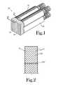
- FIG. 1a perspective view of a detector fabricated using the method of the present invention
- FIG. 2illustrates a portion of the detector of FIG. 1 , shown in section taken at 2 - 2 of FIG. 1 ;
- FIG. 3illustrates the method of the present invention wherein a laser source is used to focus a laser beam in the target media to ablate the target media at a selected location to form a void;
- FIG. 4illustrates a detector fabricated using the method of the present invention, the detector being used for detecting depth of interaction
- FIG. 5illustrates a detector fabricated using the method of the present invention, the detector being used for over sampling
- FIG. 6illustrates a detector fabricated using the method of the present invention, the detector defining hexagonal segments
- FIG. 7illustrates a detector fabricated using the method of the present invention, the detector defining octagonal and square segments;
- FIG. 8illustrates a side elevation of a detector fabricated using the method of the present invention, the detector defining optical boundaries of varying heights
- FIG. 9is a side elevation of a light guide shown relative to a scintillator, the light guide showing several variations of configurations of optical boundaries defined therein;
- FIG. 10is an end view of a circular light guide, where the method of the present invention is used to define optical boundaries at selected locations within the light guide;
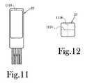
- FIG. 11is an elevation view of an optical sensor defining optical boundaries formed using the method of the present invention.
- FIG. 12is a top end view of the optical sensor of FIG. 11 , wherein the optical sensor is optically-segmented using the method of the present invention.
- a method for the fabrication of detector componentsis described herein.
- the method of the present inventionuses laser technology to create a series of optical scatter centers, or micro-voids, within a scintillation material in order to form optically-segmented virtual resolution elements with characteristics similar to detector arrays fabricated using the methods of the prior art.
- An optically-segmented light guidemay be fabricated using the method of the present invention as well.
- FIG. 1Illustrated in FIG. 1 is a perspective view of a detector component 10 fabricated using the method of the present invention, shown in relation to an array of photomultiplier tubes (PMTs) 20 .
- the detector component 10 of the present inventionis fabricated from a target media in which a plurality of micro-voids 12 (see FIG. 2 ) is defined to collectively function to manipulate light waves to enhance the control and collection of the resultant scintillation light, allowing for the accurate decoding of the impinging radiation.
- the micro-voids 12are positioned to define the optical boundaries 14 of the optically-segmented portions 16 of the detector component 10 .
- the configurations for the relative disposition of the micro-voids 12are endless.
- the micro-voids 12may be disposed in varying sizes in a specific uniform pattern, or may be randomly placed, or may form over-sampled optically-segmented virtual resolution elements.
- the micro-voids 12may be disposed in single or multiple layers, or may be randomly scattered within a given volume.
- the micro-voids 12may be disposed in planar, curvilinear, or other geometrically-arranged configurations.
- the optically-segmented portions 16 of the detector component 10may define various cross-sectional configurations other than square.
- the optically-segmented portions 16may define, but are not limited to, triangular, trapezoidal, or hexagonal configurations.
- the optically-segmented portions 16may define a combination of configurations, such as octagons and squares. Further, the optically-segmented portions 16 may define varying cross-sections as they progress from one end of an optically-segmented portion 16 to the other, including transitioning from one geometric shape to another, and/or transitioning from one size to another.
- the various configurationsare dependent upon various factors, but are selected to function with similar or improved results as compared to reflective surfaces provided in prior art devices. While specific configurations have been mentioned, the present disclosure is not intended to be limited by such configurations. Such configurations are described merely to accentuate the limitless number of configurations which may be incorporated to achieve the present invention.
- FIG. 2illustrates, in section, a portion of the detector component 10 shown in FIG. 1 . Illustrated is an array of non-contiguous, independent micro-voids 12 formed using the method of the present invention.
- the micro-voids 12 in this embodimentare disposed in a single layer and are arranged in a honeycomb pattern.
- a vertical layer 14 Vrepresentsative of a vertical optical boundary—of micro-voids 12 is illustrated.
- a single row 14 H of micro-voids 12representative of a horizontal layer.
- the micro-voids 12may alternatively be arranged in any other pattern, or configuration, or may be disposed randomly.
- FIG. 3illustrates more clearly the method of the present invention, wherein the plurality of the micro-voids 12 is formed.
- the position of each micro-void 12 within the detector component 10is determined as required.
- a selected micro-void 12is being formed at location (x, y, z) using a local coordinate system.
- the micro-voids 12are formed in a spatial surface 14 defined in the medium 10 to form an optical boundary.
- surface 14is a plane; however, non-rectilinear surfaces are also possible.
- a laser source 30is used to generate and focus a beam 32 of light into a target media 10 at the location (x, y, z).
- the laser source 30yields a laser beam 32 of sufficient power to alter the optical properties of the detector component 10 at the focal point, thereby yielding the micro-void 12 .
- the target media 10 used in the present inventionis either of a scintillator, a light-transmitting object (or light guide), or both.
- the light-transmitting objectincludes any configuration including but not limited to a block, optical fiber(s), optical tube(s), and the entrance window of an optical sensor.
- the target media 10is fabricated from a material that does not absorb in the wavelength of the laser beam 32 .
- the intense energy collecting at the focal point of the laser beam 32creates a micro-void 12 within the target media 10 that extends outward in all directions from the point of origin.
- the micro-voids 12are on the order of tens of microns in cross-section.
- the size of the micro-void 12may be larger or smaller according to design.
- the laser source 30is controlled and systematically pulsed while the laser beam 32 is concurrently and incrementally repositioned and refocused to create the predetermined disposition of each micro-void 12 within the target media 10 , whether patterned or disposed at random.
- the method of the present inventionremoves the geometric limitations as described in the background of the related art.
- the method of the present inventionis capable of fabricating detector components 10 such as scintillators and light transmitting objects having rectilinear geometry.
- the method of the present inventionis useful in fabricating detector components 10 defining more complex, multifaceted geometry, such as hexagonal and octagonal. Additionally, wavelike or curvilinear structures are also readily made available.
- Internalized geometry, generated by the focused laser beam 32eliminate the extensive labor costs associated with the current detector production and require no additional effort when substituting non-rectilinear forms into the process or when increasing the number of internalized features.
- this technologyallows for other light distributing geometry to be incorporated within the media, including optically collimating, focusing, splitting, or scattering geometries.
- FIG. 4illustrates a detector 410 fabricated using the method of the present invention.
- the detector 410 of the illustrated embodimentis a depth of interaction design (DOI).
- DOIdepth of interaction design
- the upper portion 410 U of the detector 410is optically-segmented into a 3 ⁇ 3 grid array and the lower portion 410 L of the detector 410 is optically-segmented into a 2 ⁇ 2 grid array.
- the optical boundaries 414 of the grid arraysare formed using the method of the present invention.
- the DOI detectordefines optically-segmented portions 416 configured in such a manner as to allow for the discernment of depth at which the scintillation material emits light when struck by radiation.
- an array of optical sensors 20such as avalanche photodiodes (APDs) collects the lower energy scintillation light.
- APDsavalanche photodiodes
- FIG. 5illustrates a further embodiment of a detector 510 fabricated using the method of the present invention.
- the illustrated embodiment of FIG. 5is a monolithic detector design utilizing over sampling to achieve higher resolution.
- the feature densitydoes not equate to intrinsic spatial resolution, but to virtual resolution elements that may be over-sampled.
- the spacing between the optical boundaries 514is varied such that blocks of four segments 516 are separated from each other and are bounded by a layer 514 of micro-voids 12 defining a substantially planar configuration.
- this layer 514may be substantially two-dimensional or may define a thickness such that it defines a more pronounced thickness, or third dimension.
- the individual blocks of four segments 516are themselves separated from each other.
- This separationcan be accomplished with at least one layer 514 of micro-voids 12 . Illustrated are three such layers 514 in order to accomplish a larger separation between the blocks of four segments 516 .
- conventional hardwaresuch as PMTs and APDs is used in association with the over-sampling detector, as illustrated.
- FIGS. 6 and 7illustrate two detector components 610 , 710 having non-rectilinear configurations.
- FIG. 6illustrates an array of cells 616 defined by hexagonally-disposed optical boundaries 614 .
- FIG. 7illustrates and array of octagonal optically-segmented portions 716 alternating with square cells 716 ′. While several arrangements have been illustrated, it will be understood that the present invention is not limited to these few configurations. To this extent, it will be understood that the illustrated embodiments are disclosed as exemplifying the myriad of configurations contemplated by the present invention.
- FIG. 8illustrates a side elevation of a detector component 810 fabricated using the method of the present invention.
- the illustrated component 810defines optical boundaries 814 of varying heights, similar to conventional detectors of the prior art.
- a detector 910includes a scintillator 910 A and a light guide 910 B.
- the light guide 10 Bis shown with various exemplary optical boundary 916 configurations. Specifically, illustrated three optical boundaries 916 . These boundaries 916 include orthogonally disposed planar optical boundaries 916 A, optical boundaries disposed to form a pyramidal disposition 916 B for focusing or defocusing, and optical boundaries 916 C defining compound curves. While three specific embodiments have been illustrated, it will be understood that the present invention is not intended to be limited to such disclosures.
- FIG. 10Illustrated in FIG. 10 is an end view of a circular light guide 1010 .
- a circular light guide 1010Disposed within the circular light guide 1010 are scintillators 10 A.
- Optical sensors 20are disposed about the circular light guide 1010 .
- the circular light guide 1010is optically-segmented at specified intervals by optical boundaries 1014 to define optically-segmented portions 1016 . In so doing, scintillation light is prevented from scattering throughout the entire circumference of the light guide 1010 , which in turn prevents or at least reduces pile-up errors and minimizes the dead-time of the detector system.
- FIGS. 11 and 12illustrated in FIGS. 11 and 12 is an optical sensor 20 defining optical boundaries 1114 formed using the method of the present invention.
- the entrance window of the optical sensor 20 in the illustrated embodimentis optically segmented into four quadrants, which reduces cross-talk between the channels in a multi-anode PMT.
- the method of the present inventionyields a detector component such as a scintillator, light guide or optical sensor which provides for the internal manipulation of light waves via the strategic formation of micro-voids in a way as to enhance the control and collection of the resultant scintillation light, allowing for the accurate decoding of the impinging radiation.
- detectors and light guides fabricated using the method of the present inventionhave been disclosed.
- the present inventionprovides a method for fabricating an optically-segmented detector and/or light guide using laser technology. A laser source is used to ablate a target media in a plurality of pre-selected locations.
- optical boundariesare formed within the target media to define a plurality of segments or cells.
- the cellsdefine any selected configuration(s) as required for a particular application.
- the resulting detectors and light guidesrequire less time and expense to manufacture over conventional detectors and light guides. Further, detectors and light guides fabricated using the method of the present invention are not subject to the physical constraints associated with the fabrication of conventional detectors and light guides.
- a higher packing fraction in a detector blockis achieved over conventional manufacturing methods. This results from the smaller relative size of the micro-voids as compared to the kerf resulting from cutting a scintillator in the prior art methods.
- the method of the present inventionaccomplishes a near 100% packing fraction, thus maximizing the sensitivity of the detector.
- this material handlingis minimized, thus substantially reducing the risks associated with the manufacture of the detector components. Further, contamination of the detector during the manufacturing process has been eliminated. This is due in part to the fact that there are no kerfs into which contamination may be introduced, further in part to the elimination of the need for a packing material used in the prior art methods.
- the method of the present inventionis not limited by geometric constraints presented in the methods of the present invention. As such, flat planar reflective surfaces are not required.
- optically-segmented portions of the detectorare not limited to rectangular configurations. Nor are the optically-segmented portions limited to constant cross-sectional shapes and sizes from one surface of the detector to the opposite surface.
- the method of the present inventionallows for the formation of optically-segmented portions of varying shapes and sizes, including optically-segmented portions transitioning from one shape and/or size to another. Because the optically-segmented portions are being defined within a detector without being individually cut, it will be seen that the need for handling small pixel elements is eliminated. Thus, the manufacture of high resolution detectors has been made feasible with high output while also reducing the manufacturing costs.
Landscapes
- Health & Medical Sciences (AREA)
- Physics & Mathematics (AREA)
- Life Sciences & Earth Sciences (AREA)
- General Physics & Mathematics (AREA)
- High Energy & Nuclear Physics (AREA)
- Molecular Biology (AREA)
- Spectroscopy & Molecular Physics (AREA)
- Engineering & Computer Science (AREA)
- Manufacturing & Machinery (AREA)
- Ophthalmology & Optometry (AREA)
- Mechanical Engineering (AREA)
- Measurement Of Radiation (AREA)
Abstract
Description
| U.S. Pat. No. | Inventor(s) | Issue Date | |
| 3,936,645 | A. H. Iverson | Feb. 3, 1976 | |
| 4,749,863 | M. E. Casey | Jun. 7, 1988 | |
| 4,914,301 | Y. Akai | Apr. 3, 1990 | |
| 4,982,096 | H. Fujii et al. | Jan. 1, 1991 | |
| 5,059,800 | M. K. Cueman et al. | Oct. 22, 1991 | |
| 5,453,623 | W. H. Wong et al. | Sep. 26, 1995 | |
| 6,292,529 | S. Marcovici et al. | Sep. 18, 2001 | |
| U.S. Pat. No. | Inventor(s) | Issue Date | |
| 5,637,244 | A. I. Erokhin | Jun. 10, 1997 | |
| 5,786,560 | A. Tatah et al. | Jul. 28, 1998 | |
| 5,886,318 | A. V. Vasiliev et al. | Mar. 23, 1999 | |
| 6,399,914 | I. Troitski | Jun. 4, 2002 | |
| 6,417,485 | I. Troitski | Jul. 9, 2002 | |
| 6,426,480 | I. Troitski | Jul. 30, 2002 | |
| 6,727,460 | I. Troitski | Apr. 27, 2004 | |
Claims (19)
Priority Applications (1)
| Application Number | Priority Date | Filing Date | Title |
|---|---|---|---|
| US10/856,225US8470214B2 (en) | 2003-05-30 | 2004-05-28 | Method for fabrication of a detector component using laser technology |
Applications Claiming Priority (2)
| Application Number | Priority Date | Filing Date | Title |
|---|---|---|---|
| US47443003P | 2003-05-30 | 2003-05-30 | |
| US10/856,225US8470214B2 (en) | 2003-05-30 | 2004-05-28 | Method for fabrication of a detector component using laser technology |
Publications (2)
| Publication Number | Publication Date |
|---|---|
| US20040262526A1 US20040262526A1 (en) | 2004-12-30 |
| US8470214B2true US8470214B2 (en) | 2013-06-25 |
Family
ID=33511601
Family Applications (1)
| Application Number | Title | Priority Date | Filing Date |
|---|---|---|---|
| US10/856,225Active2026-06-09US8470214B2 (en) | 2003-05-30 | 2004-05-28 | Method for fabrication of a detector component using laser technology |
Country Status (6)
| Country | Link |
|---|---|
| US (1) | US8470214B2 (en) |
| EP (1) | EP1654111B1 (en) |
| JP (1) | JP5013864B2 (en) |
| ES (1) | ES2784538T3 (en) |
| HU (1) | HUE048623T2 (en) |
| WO (1) | WO2004109870A2 (en) |
Cited By (3)
| Publication number | Priority date | Publication date | Assignee | Title |
|---|---|---|---|---|
| US20110121192A1 (en)* | 2008-05-08 | 2011-05-26 | Hamamatsu Photonics K.K. | Scintillator, method for manufacturing scintillator, and radiation detector |
| WO2021056003A1 (en) | 2019-09-20 | 2021-03-25 | Siemens Medical Solutions Usa, Inc. | Hybrid lased/air coupled pet block detector |
| US11029418B2 (en) | 2017-09-06 | 2021-06-08 | The United States Of America, As Represented By The Secretary, Department Of Health And Human Services | Micro-dose calibrator |
Families Citing this family (31)
| Publication number | Priority date | Publication date | Assignee | Title |
|---|---|---|---|---|
| US20050023473A1 (en)* | 2003-08-01 | 2005-02-03 | Burr Kent Charles | System and method for reducing optical crosstalk in multi-anode photomultiplier tube |
| US7709805B2 (en)* | 2003-08-01 | 2010-05-04 | General Electric Company | Method for generating optical anisotropy in scintillators using pulsed lasers |
| US7551712B2 (en)* | 2006-04-20 | 2009-06-23 | General Electric Company | CT detector with non-rectangular cells |
| JP2007292597A (en)* | 2006-04-25 | 2007-11-08 | Hitachi Chem Co Ltd | Radiation detector |
| US7737408B2 (en)* | 2007-07-24 | 2010-06-15 | Siemens Medical Solutions Usa, Inc. | Monolithic scintillators with optical fiber read-out |
| JP5080910B2 (en)* | 2007-09-03 | 2012-11-21 | 国立大学法人東北大学 | Array manufacturing method, scintillator array |
| WO2010041313A1 (en)* | 2008-10-08 | 2010-04-15 | 独立行政法人放射線医学総合研究所 | Doi type radiation detector |
| JP2011048081A (en)* | 2009-08-26 | 2011-03-10 | Sony Corp | Optical element, reflection reducing working device, and reflection reducing working method |
| CN102655813B (en) | 2009-10-27 | 2015-08-12 | 华盛顿大学商业中心 | Optical interface patterning for radiation detector crystals |
| US9513387B2 (en)* | 2010-02-01 | 2016-12-06 | Siemens Aktiengesellschaft | System and method for providing depth of interaction detection using positron emission tomography |
| US8357903B2 (en)* | 2010-10-19 | 2013-01-22 | Kabushiki Kaisha Toshiba | Segmented detector array |
| US8247780B2 (en)* | 2010-11-10 | 2012-08-21 | Siemens Aktiengesellschaft | High density, proportional-mode, APD arrays for individual scintillator readout in PET applications |
| JP2012127734A (en)* | 2010-12-14 | 2012-07-05 | Fujifilm Corp | Grid for imaging radiation image, method for manufacturing the grid, and radiation image imaging system |
| US8809794B2 (en) | 2011-02-02 | 2014-08-19 | Hamamatsu Photonics K.K. | Radiation detector |
| JP5739683B2 (en)* | 2011-02-03 | 2015-06-24 | 浜松ホトニクス株式会社 | Scintillator, radiation detector, and scintillator manufacturing method |
| DE102011076358B4 (en)* | 2011-05-24 | 2016-11-03 | Siemens Healthcare Gmbh | Computer tomography system with integrating and counting detector elements |
| US9194959B2 (en)* | 2011-07-06 | 2015-11-24 | Siemens Medical Solutions Usa, Inc. | Positron emission tomography detector based on monolithic scintillator crystal |
| JP5922933B2 (en)* | 2012-01-23 | 2016-05-24 | 浜松ホトニクス株式会社 | Laser processing method, laser processing apparatus, and manufacturing method of scintillator structure |
| JP2014035296A (en)* | 2012-08-09 | 2014-02-24 | Canon Inc | Radiographic device and radiographic system |
| KR101582021B1 (en)* | 2012-08-30 | 2015-12-31 | 엔지케이 인슐레이터 엘티디 | Composite substrates, a method of producing the same, a method of producing a functional layer of a nitride of a group 13 element and functional devices |
| CN105190360B (en) | 2013-05-08 | 2019-06-28 | 皇家飞利浦有限公司 | Gamma radiation detecting devices |
| EP3047308B1 (en)* | 2013-09-18 | 2020-11-11 | Koninklijke Philips N.V. | Laser etched scintillation crystals for increased performance |
| JP2016033450A (en)* | 2014-07-30 | 2016-03-10 | 国立研究開発法人放射線医学総合研究所 | Radiation detector |
| US9709684B2 (en)* | 2014-12-15 | 2017-07-18 | General Electric Company | Systems and methods for scintillators having micro-crack surfaces |
| US9753149B2 (en) | 2015-01-30 | 2017-09-05 | Hamamatsu Photonics K.K. | Radiation detector |
| US9804277B2 (en) | 2015-01-30 | 2017-10-31 | Hamamatsu Photonics K.K. | Radiation detector |
| US10094937B2 (en) | 2015-01-30 | 2018-10-09 | Hamamatsu Photonics K.K. | Radiation detector |
| US20170184728A1 (en)* | 2015-12-29 | 2017-06-29 | General Electric Company | Scintillator configurations and methods for fabricating the same |
| ES2665888B1 (en)* | 2016-09-28 | 2019-02-07 | Univ Madrid Carlos Iii | CENTELLEADORA CELL |
| KR102679432B1 (en)* | 2021-12-22 | 2024-06-28 | 주식회사 브라이토닉스이미징 | Scintillator detector and positron emission tomography apparatus using the same |
| US12013503B2 (en)* | 2022-10-07 | 2024-06-18 | Cintilight, Llc | Lateral crystal photodiode readouts and switched diode networks for processing nuclear events |
Citations (21)
| Publication number | Priority date | Publication date | Assignee | Title |
|---|---|---|---|---|
| US3936645A (en) | 1974-03-25 | 1976-02-03 | Radiologic Sciences, Inc. | Cellularized Luminescent structures |
| US4749863A (en) | 1984-12-04 | 1988-06-07 | Computer Technology And Imaging, Inc. | Two-dimensional photon counting position encoder system and process |
| US4914301A (en) | 1987-04-21 | 1990-04-03 | Kabushiki Kaisha Toshiba | X-ray detector |
| US4982096A (en) | 1988-01-06 | 1991-01-01 | Hitachi Medical Corporation | Multi-element radiation detector |
| US5047642A (en)* | 1989-10-12 | 1991-09-10 | Commissariat A L'energie Atomique | Radioluminescent screen with an improved quality factor and spatial resolution for X or gamma photon imaging |
| US5059800A (en) | 1991-04-19 | 1991-10-22 | General Electric Company | Two dimensional mosaic scintillation detector |
| US5453623A (en) | 1992-05-13 | 1995-09-26 | Board Of Regents, The University Of Texas System | Positron emission tomography camera with quadrant-sharing photomultipliers and cross-coupled scintillating crystals |
| JPH0961536A (en) | 1995-08-28 | 1997-03-07 | Canon Inc | Semiconductor radiation detection apparatus and manufacturing method thereof |
| US5673244A (en) | 1995-12-28 | 1997-09-30 | Samsung Electronics Co., Ltd. | Disk loading and magnetic head lifting mechanism using a single power source for a minidisk player |
| US5786560A (en) | 1995-03-31 | 1998-07-28 | Panasonic Technologies, Inc. | 3-dimensional micromachining with femtosecond laser pulses |
| US5886318A (en) | 1995-11-03 | 1999-03-23 | Vasiliev; Anatoly Valentinovich | Method for laser-assisted image formation in transparent objects |
| WO2000032349A1 (en)* | 1998-12-03 | 2000-06-08 | Universal Crystal Ltd. | Material processing applications of lasers using optical breakdown |
| US6151769A (en)* | 1995-05-31 | 2000-11-28 | Battelle Memorial Institute | Method of making a scintillator waveguide |
| US6292529B1 (en) | 1999-12-15 | 2001-09-18 | Analogic Corporation | Two-dimensional X-ray detector array for CT applications |
| JP2001283731A (en) | 2000-03-29 | 2001-10-12 | Hamamatsu Photonics Kk | Phosphor layer and manufacturing method threfor |
| US6399914B1 (en) | 2000-07-10 | 2002-06-04 | Igor Troitski | Method and laser system for production of high quality laser-induced damage images by using material processing made before and during image creation |
| US6417485B1 (en) | 2000-05-30 | 2002-07-09 | Igor Troitski | Method and laser system controlling breakdown process development and space structure of laser radiation for production of high quality laser-induced damage images |
| US6426480B1 (en) | 2000-08-30 | 2002-07-30 | Igor Troitski | Method and laser system for production of high quality single-layer laser-induced damage portraits inside transparent material |
| US6727460B2 (en) | 2002-02-14 | 2004-04-27 | Troitski | System for high-speed production of high quality laser-induced damage images inside transparent materials |
| US6796148B1 (en)* | 1999-09-30 | 2004-09-28 | Corning Incorporated | Deep UV laser internally induced densification in silica glasses |
| US20050023733A1 (en)* | 2003-08-01 | 2005-02-03 | Burr Kent Charles | Method for generating optical anisotropy in scintillators using pulsed lasers |
Family Cites Families (4)
| Publication number | Priority date | Publication date | Assignee | Title |
|---|---|---|---|---|
| US5391879A (en)* | 1993-11-19 | 1995-02-21 | Minnesota Mining And Manufacturing Company | Radiation detector |
| US5956382A (en)* | 1997-09-25 | 1999-09-21 | Eliezer Wiener-Avnear, Doing Business As Laser Electro Optic Application Technology Comp. | X-ray imaging array detector and laser micro-milling method for fabricating array |
| JP3967090B2 (en)* | 2001-05-16 | 2007-08-29 | 独立行政法人科学技術振興機構 | How to move voids inside transparent solids |
| JP2003020258A (en)* | 2001-07-05 | 2003-01-24 | Japan Science & Technology Corp | Microcavity processing method and apparatus for transparent dielectric object using light |
- 2004
- 2004-05-28JPJP2006515021Apatent/JP5013864B2/ennot_activeExpired - Lifetime
- 2004-05-28EPEP04753788.1Apatent/EP1654111B1/ennot_activeExpired - Lifetime
- 2004-05-28WOPCT/US2004/017033patent/WO2004109870A2/enactiveApplication Filing
- 2004-05-28USUS10/856,225patent/US8470214B2/enactiveActive
- 2004-05-28HUHUE04753788Apatent/HUE048623T2/enunknown
- 2004-05-28ESES04753788Tpatent/ES2784538T3/ennot_activeExpired - Lifetime
Patent Citations (21)
| Publication number | Priority date | Publication date | Assignee | Title |
|---|---|---|---|---|
| US3936645A (en) | 1974-03-25 | 1976-02-03 | Radiologic Sciences, Inc. | Cellularized Luminescent structures |
| US4749863A (en) | 1984-12-04 | 1988-06-07 | Computer Technology And Imaging, Inc. | Two-dimensional photon counting position encoder system and process |
| US4914301A (en) | 1987-04-21 | 1990-04-03 | Kabushiki Kaisha Toshiba | X-ray detector |
| US4982096A (en) | 1988-01-06 | 1991-01-01 | Hitachi Medical Corporation | Multi-element radiation detector |
| US5047642A (en)* | 1989-10-12 | 1991-09-10 | Commissariat A L'energie Atomique | Radioluminescent screen with an improved quality factor and spatial resolution for X or gamma photon imaging |
| US5059800A (en) | 1991-04-19 | 1991-10-22 | General Electric Company | Two dimensional mosaic scintillation detector |
| US5453623A (en) | 1992-05-13 | 1995-09-26 | Board Of Regents, The University Of Texas System | Positron emission tomography camera with quadrant-sharing photomultipliers and cross-coupled scintillating crystals |
| US5786560A (en) | 1995-03-31 | 1998-07-28 | Panasonic Technologies, Inc. | 3-dimensional micromachining with femtosecond laser pulses |
| US6151769A (en)* | 1995-05-31 | 2000-11-28 | Battelle Memorial Institute | Method of making a scintillator waveguide |
| JPH0961536A (en) | 1995-08-28 | 1997-03-07 | Canon Inc | Semiconductor radiation detection apparatus and manufacturing method thereof |
| US5886318A (en) | 1995-11-03 | 1999-03-23 | Vasiliev; Anatoly Valentinovich | Method for laser-assisted image formation in transparent objects |
| US5673244A (en) | 1995-12-28 | 1997-09-30 | Samsung Electronics Co., Ltd. | Disk loading and magnetic head lifting mechanism using a single power source for a minidisk player |
| WO2000032349A1 (en)* | 1998-12-03 | 2000-06-08 | Universal Crystal Ltd. | Material processing applications of lasers using optical breakdown |
| US6796148B1 (en)* | 1999-09-30 | 2004-09-28 | Corning Incorporated | Deep UV laser internally induced densification in silica glasses |
| US6292529B1 (en) | 1999-12-15 | 2001-09-18 | Analogic Corporation | Two-dimensional X-ray detector array for CT applications |
| JP2001283731A (en) | 2000-03-29 | 2001-10-12 | Hamamatsu Photonics Kk | Phosphor layer and manufacturing method threfor |
| US6417485B1 (en) | 2000-05-30 | 2002-07-09 | Igor Troitski | Method and laser system controlling breakdown process development and space structure of laser radiation for production of high quality laser-induced damage images |
| US6399914B1 (en) | 2000-07-10 | 2002-06-04 | Igor Troitski | Method and laser system for production of high quality laser-induced damage images by using material processing made before and during image creation |
| US6426480B1 (en) | 2000-08-30 | 2002-07-30 | Igor Troitski | Method and laser system for production of high quality single-layer laser-induced damage portraits inside transparent material |
| US6727460B2 (en) | 2002-02-14 | 2004-04-27 | Troitski | System for high-speed production of high quality laser-induced damage images inside transparent materials |
| US20050023733A1 (en)* | 2003-08-01 | 2005-02-03 | Burr Kent Charles | Method for generating optical anisotropy in scintillators using pulsed lasers |
Non-Patent Citations (2)
| Title |
|---|
| Japanese Office Action (with English translation) dated Mar. 30, 2010. |
| Moriya et al., "Development of PET Detectors Using Monolithic Scintillation Crystals Processed with Sub-Surface Laser Engraving Technique," 2009 IEEE Nuclear Science Symposium Conference Record, pp. 3560-3564. |
Cited By (6)
| Publication number | Priority date | Publication date | Assignee | Title |
|---|---|---|---|---|
| US20110121192A1 (en)* | 2008-05-08 | 2011-05-26 | Hamamatsu Photonics K.K. | Scintillator, method for manufacturing scintillator, and radiation detector |
| US8779371B2 (en)* | 2008-05-08 | 2014-07-15 | Hamamatsu Photonics K.K. | Scintillator, method for manufacturing scintillator, and radiation detector |
| US11029418B2 (en) | 2017-09-06 | 2021-06-08 | The United States Of America, As Represented By The Secretary, Department Of Health And Human Services | Micro-dose calibrator |
| US11614548B2 (en) | 2017-09-06 | 2023-03-28 | The United States Of America, As Represented By The Secretary, Department Of Health And Human Services | Radioactive source calibration |
| WO2021056003A1 (en) | 2019-09-20 | 2021-03-25 | Siemens Medical Solutions Usa, Inc. | Hybrid lased/air coupled pet block detector |
| US12123988B2 (en) | 2019-09-20 | 2024-10-22 | Siemens Medical Solutions Usa, Inc. | Hybrid lased/air coupled PET block detector |
Also Published As
| Publication number | Publication date |
|---|---|
| HUE048623T2 (en) | 2020-08-28 |
| WO2004109870A2 (en) | 2004-12-16 |
| ES2784538T3 (en) | 2020-09-28 |
| WO2004109870A3 (en) | 2005-12-22 |
| JP2007525652A (en) | 2007-09-06 |
| JP5013864B2 (en) | 2012-08-29 |
| EP1654111A4 (en) | 2016-09-07 |
| EP1654111B1 (en) | 2020-02-12 |
| EP1654111A2 (en) | 2006-05-10 |
| US20040262526A1 (en) | 2004-12-30 |
Similar Documents
| Publication | Publication Date | Title |
|---|---|---|
| US8470214B2 (en) | Method for fabrication of a detector component using laser technology | |
| US9442198B2 (en) | Optical-interface patterning for radiation detector crystals | |
| US5956382A (en) | X-ray imaging array detector and laser micro-milling method for fabricating array | |
| US5572034A (en) | Fiber optic plates for generating seamless images | |
| US8809794B2 (en) | Radiation detector | |
| US6344649B2 (en) | Scintillator for a multi-slice computed tomograph system | |
| JP5139881B2 (en) | Scintillator manufacturing method and radiation position detector | |
| JP5225051B2 (en) | Scintillator, radiation detector, and method of manufacturing scintillator | |
| Sabet et al. | Fabricating high-resolution and high-sensitivity scintillator arrays using Laser Induced Optical Barriers | |
| JP2020531183A (en) | Multilayer detector with monolithic scintillator | |
| US20170014943A1 (en) | System and method for processing radiation detectors using laser beams | |
| US20020190214A1 (en) | Hybride two-dimensional scintillator arrangement | |
| US6793857B2 (en) | Method for producing a one- or multidimensional detector array | |
| US8648311B2 (en) | Radiation detector | |
| US7408164B2 (en) | Detector array utilizing air gaps as a reflector between array elements | |
| JP5739683B2 (en) | Scintillator, radiation detector, and scintillator manufacturing method | |
| Sabet et al. | Laser pixelation of thick scintillators for medical imaging applications: x-ray studies | |
| JP2000098040A (en) | Method of manufacturing solid state detector for CT | |
| JP7310015B2 (en) | Hybrid laser/air coupled PET block detector | |
| US20170184728A1 (en) | Scintillator configurations and methods for fabricating the same | |
| Nagarkar et al. | Focused scintillator array for high resolution gamma ray imaging |
Legal Events
| Date | Code | Title | Description |
|---|---|---|---|
| AS | Assignment | Owner name:CTI MOLECULAR IMAGING, INC., TENNESSEE Free format text:ASSIGNMENT OF ASSIGNORS INTEREST;ASSIGNORS:MARLAR, TROY;ANDREACO, MARK S.;REEL/FRAME:015762/0556;SIGNING DATES FROM 20040825 TO 20040830 Owner name:CTI PET SYSTEMS, INC., TENNESSEE Free format text:ASSIGNMENT OF ASSIGNORS INTEREST;ASSIGNORS:CORBEIL, JAMES L.;SCHMAND, MATTHIAS J.;DOSHI, NIRAJ K.;REEL/FRAME:015762/0559 Effective date:20040830 Owner name:CTI MOLECULAR IMAGING, INC., TENNESSEE Free format text:ASSIGNMENT OF ASSIGNORS INTEREST;ASSIGNORS:MARLAR, TROY;ANDREACO, MARK S.;SIGNING DATES FROM 20040825 TO 20040830;REEL/FRAME:015762/0556 | |
| AS | Assignment | Owner name:SIEMENS MEDICAL SOLUTIONS USA, INC.,PENNSYLVANIA Free format text:MERGER;ASSIGNOR:CTI PET SYSTEMS, INC.;REEL/FRAME:018535/0183 Effective date:20060930 Owner name:SIEMENS MEDICAL SOLUTIONS USA, INC., PENNSYLVANIA Free format text:MERGER;ASSIGNOR:CTI PET SYSTEMS, INC.;REEL/FRAME:018535/0183 Effective date:20060930 | |
| STCF | Information on status: patent grant | Free format text:PATENTED CASE | |
| FPAY | Fee payment | Year of fee payment:4 | |
| MAFP | Maintenance fee payment | Free format text:PAYMENT OF MAINTENANCE FEE, 8TH YEAR, LARGE ENTITY (ORIGINAL EVENT CODE: M1552); ENTITY STATUS OF PATENT OWNER: LARGE ENTITY Year of fee payment:8 | |
| MAFP | Maintenance fee payment | Free format text:PAYMENT OF MAINTENANCE FEE, 12TH YEAR, LARGE ENTITY (ORIGINAL EVENT CODE: M1553); ENTITY STATUS OF PATENT OWNER: LARGE ENTITY Year of fee payment:12 |