US8466073B2 - Capping layer for reduced outgassing - Google Patents
Capping layer for reduced outgassingDownload PDFInfo
- Publication number
- US8466073B2 US8466073B2US13/448,624US201213448624AUS8466073B2US 8466073 B2US8466073 B2US 8466073B2US 201213448624 AUS201213448624 AUS 201213448624AUS 8466073 B2US8466073 B2US 8466073B2
- Authority
- US
- United States
- Prior art keywords
- silicon
- precursor
- layer
- oxygen
- nitrogen
- Prior art date
- Legal status (The legal status is an assumption and is not a legal conclusion. Google has not performed a legal analysis and makes no representation as to the accuracy of the status listed.)
- Expired - Fee Related
Links
Images


Classifications
- H—ELECTRICITY
- H01—ELECTRIC ELEMENTS
- H01L—SEMICONDUCTOR DEVICES NOT COVERED BY CLASS H10
- H01L21/00—Processes or apparatus adapted for the manufacture or treatment of semiconductor or solid state devices or of parts thereof
- H01L21/02—Manufacture or treatment of semiconductor devices or of parts thereof
- H01L21/02104—Forming layers
- H01L21/02107—Forming insulating materials on a substrate
- H01L21/02109—Forming insulating materials on a substrate characterised by the type of layer, e.g. type of material, porous/non-porous, pre-cursors, mixtures or laminates
- H01L21/022—Forming insulating materials on a substrate characterised by the type of layer, e.g. type of material, porous/non-porous, pre-cursors, mixtures or laminates the layer being a laminate, i.e. composed of sublayers, e.g. stacks of alternating high-k metal oxides
- C—CHEMISTRY; METALLURGY
- C23—COATING METALLIC MATERIAL; COATING MATERIAL WITH METALLIC MATERIAL; CHEMICAL SURFACE TREATMENT; DIFFUSION TREATMENT OF METALLIC MATERIAL; COATING BY VACUUM EVAPORATION, BY SPUTTERING, BY ION IMPLANTATION OR BY CHEMICAL VAPOUR DEPOSITION, IN GENERAL; INHIBITING CORROSION OF METALLIC MATERIAL OR INCRUSTATION IN GENERAL
- C23C—COATING METALLIC MATERIAL; COATING MATERIAL WITH METALLIC MATERIAL; SURFACE TREATMENT OF METALLIC MATERIAL BY DIFFUSION INTO THE SURFACE, BY CHEMICAL CONVERSION OR SUBSTITUTION; COATING BY VACUUM EVAPORATION, BY SPUTTERING, BY ION IMPLANTATION OR BY CHEMICAL VAPOUR DEPOSITION, IN GENERAL
- C23C16/00—Chemical coating by decomposition of gaseous compounds, without leaving reaction products of surface material in the coating, i.e. chemical vapour deposition [CVD] processes
- C23C16/22—Chemical coating by decomposition of gaseous compounds, without leaving reaction products of surface material in the coating, i.e. chemical vapour deposition [CVD] processes characterised by the deposition of inorganic material, other than metallic material
- C23C16/30—Deposition of compounds, mixtures or solid solutions, e.g. borides, carbides, nitrides
- C—CHEMISTRY; METALLURGY
- C23—COATING METALLIC MATERIAL; COATING MATERIAL WITH METALLIC MATERIAL; CHEMICAL SURFACE TREATMENT; DIFFUSION TREATMENT OF METALLIC MATERIAL; COATING BY VACUUM EVAPORATION, BY SPUTTERING, BY ION IMPLANTATION OR BY CHEMICAL VAPOUR DEPOSITION, IN GENERAL; INHIBITING CORROSION OF METALLIC MATERIAL OR INCRUSTATION IN GENERAL
- C23C—COATING METALLIC MATERIAL; COATING MATERIAL WITH METALLIC MATERIAL; SURFACE TREATMENT OF METALLIC MATERIAL BY DIFFUSION INTO THE SURFACE, BY CHEMICAL CONVERSION OR SUBSTITUTION; COATING BY VACUUM EVAPORATION, BY SPUTTERING, BY ION IMPLANTATION OR BY CHEMICAL VAPOUR DEPOSITION, IN GENERAL
- C23C16/00—Chemical coating by decomposition of gaseous compounds, without leaving reaction products of surface material in the coating, i.e. chemical vapour deposition [CVD] processes
- C23C16/44—Chemical coating by decomposition of gaseous compounds, without leaving reaction products of surface material in the coating, i.e. chemical vapour deposition [CVD] processes characterised by the method of coating
- C23C16/448—Chemical coating by decomposition of gaseous compounds, without leaving reaction products of surface material in the coating, i.e. chemical vapour deposition [CVD] processes characterised by the method of coating characterised by the method used for generating reactive gas streams, e.g. by evaporation or sublimation of precursor materials
- C23C16/452—Chemical coating by decomposition of gaseous compounds, without leaving reaction products of surface material in the coating, i.e. chemical vapour deposition [CVD] processes characterised by the method of coating characterised by the method used for generating reactive gas streams, e.g. by evaporation or sublimation of precursor materials by activating reactive gas streams before their introduction into the reaction chamber, e.g. by ionisation or addition of reactive species
- C—CHEMISTRY; METALLURGY
- C23—COATING METALLIC MATERIAL; COATING MATERIAL WITH METALLIC MATERIAL; CHEMICAL SURFACE TREATMENT; DIFFUSION TREATMENT OF METALLIC MATERIAL; COATING BY VACUUM EVAPORATION, BY SPUTTERING, BY ION IMPLANTATION OR BY CHEMICAL VAPOUR DEPOSITION, IN GENERAL; INHIBITING CORROSION OF METALLIC MATERIAL OR INCRUSTATION IN GENERAL
- C23C—COATING METALLIC MATERIAL; COATING MATERIAL WITH METALLIC MATERIAL; SURFACE TREATMENT OF METALLIC MATERIAL BY DIFFUSION INTO THE SURFACE, BY CHEMICAL CONVERSION OR SUBSTITUTION; COATING BY VACUUM EVAPORATION, BY SPUTTERING, BY ION IMPLANTATION OR BY CHEMICAL VAPOUR DEPOSITION, IN GENERAL
- C23C16/00—Chemical coating by decomposition of gaseous compounds, without leaving reaction products of surface material in the coating, i.e. chemical vapour deposition [CVD] processes
- C23C16/56—After-treatment
- H—ELECTRICITY
- H01—ELECTRIC ELEMENTS
- H01L—SEMICONDUCTOR DEVICES NOT COVERED BY CLASS H10
- H01L21/00—Processes or apparatus adapted for the manufacture or treatment of semiconductor or solid state devices or of parts thereof
- H01L21/02—Manufacture or treatment of semiconductor devices or of parts thereof
- H01L21/02104—Forming layers
- H01L21/02107—Forming insulating materials on a substrate
- H01L21/02109—Forming insulating materials on a substrate characterised by the type of layer, e.g. type of material, porous/non-porous, pre-cursors, mixtures or laminates
- H01L21/02112—Forming insulating materials on a substrate characterised by the type of layer, e.g. type of material, porous/non-porous, pre-cursors, mixtures or laminates characterised by the material of the layer
- H01L21/02123—Forming insulating materials on a substrate characterised by the type of layer, e.g. type of material, porous/non-porous, pre-cursors, mixtures or laminates characterised by the material of the layer the material containing silicon
- H01L21/02164—Forming insulating materials on a substrate characterised by the type of layer, e.g. type of material, porous/non-porous, pre-cursors, mixtures or laminates characterised by the material of the layer the material containing silicon the material being a silicon oxide, e.g. SiO2
- H—ELECTRICITY
- H01—ELECTRIC ELEMENTS
- H01L—SEMICONDUCTOR DEVICES NOT COVERED BY CLASS H10
- H01L21/00—Processes or apparatus adapted for the manufacture or treatment of semiconductor or solid state devices or of parts thereof
- H01L21/02—Manufacture or treatment of semiconductor devices or of parts thereof
- H01L21/02104—Forming layers
- H01L21/02107—Forming insulating materials on a substrate
- H01L21/02109—Forming insulating materials on a substrate characterised by the type of layer, e.g. type of material, porous/non-porous, pre-cursors, mixtures or laminates
- H01L21/02205—Forming insulating materials on a substrate characterised by the type of layer, e.g. type of material, porous/non-porous, pre-cursors, mixtures or laminates the layer being characterised by the precursor material for deposition
- H01L21/02208—Forming insulating materials on a substrate characterised by the type of layer, e.g. type of material, porous/non-porous, pre-cursors, mixtures or laminates the layer being characterised by the precursor material for deposition the precursor containing a compound comprising Si
- H01L21/02211—Forming insulating materials on a substrate characterised by the type of layer, e.g. type of material, porous/non-porous, pre-cursors, mixtures or laminates the layer being characterised by the precursor material for deposition the precursor containing a compound comprising Si the compound being a silane, e.g. disilane, methylsilane or chlorosilane
- H—ELECTRICITY
- H01—ELECTRIC ELEMENTS
- H01L—SEMICONDUCTOR DEVICES NOT COVERED BY CLASS H10
- H01L21/00—Processes or apparatus adapted for the manufacture or treatment of semiconductor or solid state devices or of parts thereof
- H01L21/02—Manufacture or treatment of semiconductor devices or of parts thereof
- H01L21/02104—Forming layers
- H01L21/02107—Forming insulating materials on a substrate
- H01L21/02109—Forming insulating materials on a substrate characterised by the type of layer, e.g. type of material, porous/non-porous, pre-cursors, mixtures or laminates
- H01L21/02205—Forming insulating materials on a substrate characterised by the type of layer, e.g. type of material, porous/non-porous, pre-cursors, mixtures or laminates the layer being characterised by the precursor material for deposition
- H01L21/02208—Forming insulating materials on a substrate characterised by the type of layer, e.g. type of material, porous/non-porous, pre-cursors, mixtures or laminates the layer being characterised by the precursor material for deposition the precursor containing a compound comprising Si
- H01L21/02219—Forming insulating materials on a substrate characterised by the type of layer, e.g. type of material, porous/non-porous, pre-cursors, mixtures or laminates the layer being characterised by the precursor material for deposition the precursor containing a compound comprising Si the compound comprising silicon and nitrogen
- H—ELECTRICITY
- H01—ELECTRIC ELEMENTS
- H01L—SEMICONDUCTOR DEVICES NOT COVERED BY CLASS H10
- H01L21/00—Processes or apparatus adapted for the manufacture or treatment of semiconductor or solid state devices or of parts thereof
- H01L21/02—Manufacture or treatment of semiconductor devices or of parts thereof
- H01L21/02104—Forming layers
- H01L21/02107—Forming insulating materials on a substrate
- H01L21/02296—Forming insulating materials on a substrate characterised by the treatment performed before or after the formation of the layer
- H01L21/02318—Forming insulating materials on a substrate characterised by the treatment performed before or after the formation of the layer post-treatment
- H01L21/02321—Forming insulating materials on a substrate characterised by the treatment performed before or after the formation of the layer post-treatment introduction of substances into an already existing insulating layer
- H01L21/02323—Forming insulating materials on a substrate characterised by the treatment performed before or after the formation of the layer post-treatment introduction of substances into an already existing insulating layer introduction of oxygen
- H01L21/02326—Forming insulating materials on a substrate characterised by the treatment performed before or after the formation of the layer post-treatment introduction of substances into an already existing insulating layer introduction of oxygen into a nitride layer, e.g. changing SiN to SiON
Definitions
- Semiconductor device geometrieshave dramatically decreased in size since their introduction several decades ago. Modern semiconductor fabrication equipment routinely produce devices with 45 nm, 32 nm, and 28 nm feature sizes, and new equipment is being developed and implemented, to make devices with even smaller geometries.
- the decreasing feature sizesresult in structural features on the device having decreased spatial dimensions.
- the widths of gaps and trenches on the devicenarrow to a point where the aspect ratio of gap depth to its width becomes high enough to make it challenging to fill the gap with dielectric material.
- the depositing dielectric materialis prone to clog at the top before the gap completely fills, producing a void or seam, in the middle of the gap.
- the hardeningincludes a heat treatment to remove carbon and hydroxyl groups from the deposited material to leave behind a solid dielectric such as silicon oxide.
- a solid dielectricsuch as silicon oxide.
- the departing carbon and hydroxyl speciesoften leave behind pores in the hardened dielectric that reduce the quality of the final material.
- the hardening dielectricalso tends to shrink in volume, which can leave cracks and spaces at the interface of the dielectric and the surrounding substrate. In some instances, the volume of the hardened dielectric can decrease by 40% or more.
- SODSpin-on dielectrics
- the materialis generally converted to silicon oxide from a silazane-type film which contains silicon, nitrogen and hydrogen.
- Silicon, nitrogen and hydrogen containing filmsare typically converted to silicon oxide at high temperature in an oxygen containing environment. Oxygen from the environment displaces nitrogen and hydrogen to create the silicon oxide film.
- High temperature exposure to oxygen environmentscan min underlying films for some circuit architectures. This consideration results in the need to stay within a “thermal budget” doting a manufacturing process flow. Thermal budget considerations have largely limited SOD to process flows incorporating an underlying silicon nitride layer which can protect underlying features from oxidation (e.g. DRAM applications).
- Radical-component CVDcan create a flowable film by exciting one precursor and combining it with an unexcited silicon-containing precursor in the plasma-free substrate processing region. Film properties, including density, may change slightly in time until the silazane containing film is converted to silicon oxide. Controlling the evolution of the film properties improves the manufacturability of devices using these films. Thus, there is a need for new deposition processes and materials to form, dielectric materials which do not evolve over time. This and other needs are addressed in the present application.
- a method of forming a silicon oxide layeris described.
- the methodfirst deposits a silicon-nitrogen-and-hydrogen-containing (polysilazane) film by radical-component chemical vapor deposition (CVD).
- the silicon-nitrogen-and-hydrogen-containing filmis formed by combining a radical precursor (excited in a remote plasma) with an unexcited carbon-free silicon precursor.
- a capping layeris formed over the silicon-nitrogen-and-hydrogen-containing film to avoid time-evolution of underlying film properties prior to conversion into silicon oxide.
- the capping layeris formed by combining a radical oxygen precursor (excited in a remote plasma) with an unexcited silicon-and-carbon-containing-precursor.
- the filmsare converted to silicon oxide by exposure to oxygen-containing environments. The two films may be deposited within the same substrate processing chamber and may be deposited without breaking vacuum.
- Embodiments of the inventioninclude methods of forming a silicon oxide layer on a substrate.
- the methodsinclude forming a first layer comprising silicon, nitrogen and hydrogen by flowing an unexcited precursor into a remote plasma region, to produce a radical-precursor, combining a carbon-free silicon-containing precursor with the radical-precursor in the plasma-free substrate processing region, and depositing a carbon-free silicon-nitrogen-and-hydrogen-containing layer over the substrate.
- the methodsfurther include forming a second layer comprising silicon and carbon by flowing an unexcited oxygen-containing precursor into a remote plasma region to produce a radical-oxygen precursor, combining a silicon-and-carbon-containing precursor with the radical-oxygen precursor in the plasma-free substrate processing region, and depositing a silicon-oxygen-and-carbon-containing capping layer over the silicon-nitrogen-and-hydrogen-containing layer.
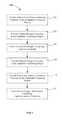
- FIG. 1is a flowchart illustrating selected steps for making a silicon, oxide film according to embodiments of the invention.
- FIG. 2shows a substrate processing system according to embodiments of the invention.
- FIG. 3Ashows a substrate processing chamber according to embodiments of the invention.
- FIG. 3Bshows a gas distribution showerhead according to embodiments of the invention.
- a method of forming a silicon oxide layeris described.
- the methodfirst deposits a silicon-nitrogen-and-hydrogen-containing (polysilazane) film by radical-component chemical vapor deposition (CVD).
- the silicon-nitrogen-and-hydrogen-containing filmis formed by combining a radical precursor (excited in a remote plasma) with an unexcited carbon-free silicon precursor.
- a capping layeris formed over the silicon-nitrogen-and-hydrogen-containing film to avoid time-evolution of underlying film properties prior to conversion into silicon oxide.
- the capping layeris formed by combining a radical oxygen precursor (excited in a remote plasma) with an unexcited silicon-and-carbon-containing-precursor.
- the filmsare converted to silicon oxide by exposure to oxygen-containing environments. The two films may be deposited within the same substrate processing chamber and may be deposited without breaking vacuum.
- Capping a radical-component CVD silicon-nitrogen-and-hydrogen-containing film with a radical-component CVD silicon-oxygen-and-carbon-containing filmhas been found to reduce and/or eliminate outgassing and concomitant evolution of film properties over time upon exposing the substrate to air. Without the silicon-oxygen-and-carbon-containing capping layer, the properties and stoichiometry of the film may change over time. The films evolve in time due to the outgassing of silicon-containing species, ammonia and the like. The properties may also evolve due to the absorption of water or other components present in the surrounding atmosphere (air) within a typical fabrication facility.
- silicon-oxygen-and-carbon-containing capping layers described hereinhave been found to suppress outgassing but still allow conversion of the underlying silicon-nitrogen-and-hydrogen-containing film to a silicon-and-oxygen-containing film and to silicon oxide.
- Radical-component CVD films capped with silicon-oxygen-and-carbon-containing films according to the methods contained hereinhave been found to exhibit properties which do not evolve when the substrate is exposed to typical cleanroom atmospheres. Additional details about the methods and systems of forming the silicon, oxide layer will now be described.
- FIG. 1is a flowchart showing selected steps in a method 100 of making silicon oxide films according to embodiments of the invention.
- the method 100includes providing a carbon-tree silicon-containing precursor to a substrate processing region 102 .
- the carbon-free silicon-containing precursordoes not pass through a plasma excitation, in embodiments, so the precursor travels into the substrate processing region intact. Excitation is then provided only by the radical precursor to be described shortly.
- the carbon-free silicon-containing precursormay be, for example, a silicon-and-nitrogen-containing precursor, a silicon-and-hydrogen-containing precursor, or a silicon-nitrogen-and-hydrogen-containing precursor, among other classes of silicon precursors.
- the absence of carbonreduces the shrinkage of the deposited film.
- the silicon-containing precursormay be oxygen-free in addition to carbon-tree.
- the lack of oxygenresults in a lower concentration of silanol (Si—OH) groups in the silicon-and-nitrogen-containing layer formed from the precursors.
- Si—OHsilanol
- Excess silanol moieties in the deposited, filmcan cause increased porosity and shrinkage during post deposition steps that remove the hydroxyl (—OH) moieties from the deposited layer.
- carbon-free silicon precursorsmay include silyl-amines such as H 2 N(SiH 3 ), HN(SiH 3 ) 2 , and N(SiH 3 ) 3 , among other silyl-amines.
- the flow rates of a silylaminemay be greater than or about 200 sccm, greater than or about 300 sccm, or greater than or about 500 sccm in different embodiments. All flow rates given herein refer to a dual chamber substrate processing system. Single wafer systems would require half these flow rates and other wafer shapes/sizes would require flow rates scaled by the processed area.
- These silyl-aminesmay be mixed with additional gases that may act as carrier gases, reactive gases, or both.
- Additional gasesmay include H 2 , N 2 , NH 3 , He, Ne and/or Ar, among other gases.
- Examples of carbon-free silicon-containing precursorsmay also include silane (SiH 4 ) either alone or mixed with other silicon (e.g., N(SiH 3 ) 3 ), hydrogen (e.g., H 2 ), and/or nitrogen (e.g., N 2 , NH 3 ) containing gases.
- Carbon-free silicon-containing precursorsmay also include disilane, trisilane, even higher-order silanes, and chlorinated silanes, alone or in combination with one another or the previously mentioned carbon-free silicon-containing precursors.
- a radical precursoris also provided to the substrate processing region 104 .
- a radical precursordescribes plasma effluents produced in the plasma excitation outside the substrate processing region from any stable species (inert or reactive).
- the radical precursormay be a nitrogen-containing radical precursor which will be referred to herein as a radical-nitrogen precursor.
- the radical-nitrogen precursoris a nitrogen-radical-containing precursor that was generated outside the substrate processing region, from a more stable nitrogen precursor.
- a stable precursormay be referred to herein as an unexcited precursor to indicate that the precursor has not yet passed through a plasma.
- a stable nitrogen precursor compound containing NH 3 , hydrazine (N 2 H 4 ) and/or N 2may be activated in a chamber plasma region or another remote plasma, system (RPS) outside the processing chamber to form the radical-nitrogen precursor, which is then transported into the substrate processing region to excite the carbon-free silicon-containing precursor.
- RPSremote plasma, system
- the activation of the stable nitrogen precursor into the radical-nitrogen precursorinvolves dissociation which may be accomplished thermal dissociation, ultraviolet light dissociation, and/or plasma dissociation, among other methods.
- Plasma dissociationmay involve striking a plasma from helium, argon, hydrogen (H 2 ), xenon, ammonia (NH 3 ), etc., in a remote plasma generating chamber and introducing the stable nitrogen precursor to the plasma region to generate the radical-nitrogen precursor.
- the stable nitrogen precursormay also be a mixture comprising NH 3 & N 2 , NH 3 & H 2 , NH 3 & N 2 & H 2 and N 2 & H 2 , in different embodiments. Hydrazine may also be used in place of or in combination with NH 3 and in the mixtures involving N 2 and H 2 .
- the flow rate of the stable nitrogen precursormay be greater than or about 300 sccm, greater than or about 500 sccm or greater than or about 700 sccm in different embodiments.
- the radical-nitrogen precursor produced in the chamber plasma regionmay be one or more of .N, .H, .H 2 , etc., and may also be accompanied by ionized species formed in the plasma.
- Sources of oxygenmay also be combined with the more stable nitrogen precursor in the remote plasma in embodiments of the invention.
- the addition of a source of oxygenpre-loads the film with oxygen while decreasing flowability.
- Sources of oxygenmay include one or more of O 2 , H 2 O, O 3 , H 2 O 2 , N 2 O, NO or NO 2 .
- the radical-nitrogen precursoris generated in a section of the substrate processing region partitioned from a deposition region where the precursors mix and react to deposit the silicon-and-nitrogen-containing layer on a deposition substrate (e.g., a semiconductor wafer).
- the radical-nitrogen precursormay also be accompanied by a carrier gas such as hydrogen (H 2 ), nitrogen (N 2 ), helium, neon, argon etc.
- the substrate processing regionmay be described herein as “plasma-free” during the growth of the silicon-nitrogen-and-hydrogen-containing layer and during subsequent processes. “Plasma-free” does not necessarily mean the region is devoid of plasma.
- the borders of the plasma in the chamber plasma regionare bard to define and may encroach upon the substrate processing region through the apertures in the showerhead.
- a small amount of ionizationmay be initiated within the substrate processing region directly.
- a low intensity plasmamay be created in the substrate processing region without compromising the flowable nature of the forming film. All causes for a plasma having much lower ion density than the chamber plasma region during the creation of the radical nitrogen precursor do not deviate from the scope of “plasma-free” as used herein.
- the carbon-free silicon precursor and the radical-nitrogen precursormix and react to deposit a silicon-nitrogen-and-hydrogen-containing film on the deposition substrate 106 .
- the deposited silicon-nitrogen-and-hydrogen containing filmmay deposit conformally with some recipe combinations in embodiments. In other embodiments, the deposited silicon-nitrogen-and-hydrogen-containing film has flowable characteristics unlike conventional silicon nitride (Si 3 N 4 ) film deposition techniques. The flowable nature during formation allows the film to flow into narrow features before solidifying.
- the substrate temperaturemay be between about 0° and about 225° C., between about room temperature (25° C.) and about 125° C. or between about 40° C. and about 95° C. in embodiments of the invention. These temperature ranges also apply to the capping layer described shortly in embodiments.
- Nitrogen in the silicon-nitrogen-and-hydrogen-containing filmmay originate from either (or both) of the radical precursor or the unexcited precursor.
- the carbon-free silicon-containing precursormay be essentially nitrogen-free, in some embodiments. However, in other embodiments, both the carbon-free silicon-containing precursor and the radical-nitrogen precursor contain nitrogen.
- the radical precursormay be essentially nitrogen-free and the nitrogen for the silicon-nitrogen-and-hydrogen-containing layer may be supplied by the carbon-free silicon-containing precursor.
- the radical precursormay be referred to herein as a “radical-nitrogen-and/or-hydrogen precursor,” which means that the precursor contains nitrogen and/or hydrogen.
- the precursor flowed into the plasma region to form the radical-nitrogen-and/or-hydrogen precursormay be referred to as a nitrogen-and/or-hydrogen-containing precursor.
- This nomenclaturemay be applied to each of the embodiments disclosed herein.
- the nitrogen-and/or-hydrogen-containing precursorcomprises hydrogen (H 2 ) while the radical-nitrogen-and/or-hydrogen precursor comprises .H, etc.
- the flowability of a silicon-nitrogen-and-hydrogen-containing filmmay be due to a variety of properties which result from mixing a radical-nitrogen precursors with a carbon-free silicon-containing precursor. These properties may include a significant hydrogen component in the deposited film and/or the presence of short chained polysilazane polymers. These short chains grow and network to form more dense dielectric material during and after the formation of the film.
- the deposited filmmay have a silazane-type, Si—NH—Si backbone (i.e., a carbon-free Si—N—H film).
- the deposited silicon-nitrogen-and-hydrogen-containing filmis also substantially carbon-tree.
- carbon-freedoes not necessarily mean the film lacks even trace amounts of carbon. Carbon contaminants may be present in the precursor materials that find their way into the deposited silicon-and-nitrogen-containing precursor. The amount of these carbon impurities however are much less than would be found in a silicon precursor having a carbon moiety (e.g., tetraethylorthosilicate, tetramethyldisiloxane, etc.).
- the process effluentsmay be removed from the substrate processing region in embodiments of the invention.
- Process effluentsmay include any unreacted carbon-free silicon-containing precursor, unreacted radical-nitrogen precursor, inert carrier gases and reaction by-products from the film growth.
- the process effluentsmay be displaced by flowing inert species into the substrate processing region and/or by exhaustion through an exhaust port in disclosed embodiments.
- the substratePrior to the deposition of the capping layer, the substrate may not be exposed to air in order to further minimize any evolution of film properties.
- the method 100also includes the remote generation of a radical-oxygen precursor in a remote plasma system (RPS) outside the deposition region 108 .
- the radical-oxygen precursorincludes the plasma effluents created in the RPS and may contain atomic oxygen.
- the same RPSmay be used to create the radical-oxygen precursor of operation 108 as was used to create the radical-nitrogen precursor in operation 104 in embodiments.
- the radical-oxygen precursormay be generated by the dissociation of an oxygen containing precursor such as molecular oxygen (O 2 ), ozone (O 3 ), an nitrogen-oxygen compound (e.g., NO, NO 2 , N 2 O, etc.), a hydrogen-oxygen compound (e.g., H 2 O, H 2 O 2 , etc.), a carbon-oxygen compound (e.g., CO, CO 2 , etc.), as well as other oxygen containing precursors and combinations of precursors.
- the dissociation of the oxygen containing precursor to generate the radical-oxygen precursormay be done by the same means used to create the radical-nitrogen precursor in operation 104 .
- the radical-oxygen precursoris then introduced to the deposition chamber 108 where it may mix for the first time with a silicon-and-carbon-containing precursor, which, is also introduced to the chamber 110 .
- the radical-oxygen precursorreacts with the silicon precursor (and other deposition precursors that may be present in the reaction chamber) at moderate temperatures (e.g., reaction temperatures less than 100° C. in embodiments) and pressures (e.g., about 0.1 Torr to about 10 Torr; 0.5 to 6 Torr total chamber pressure, etc.) to form a silicon-oxygen-and-carbon-containing film 112 .
- the silicon-oxygen-and-carbon-containing filmmay be a silicon-and-oxygen-containing layer.
- the wafermay be adjusted (i.e., heated or cooled) by a wafer pedestal that supports the wafer to a temperature of about 0° C. to about 150° C.
- Process parameters described for the carbon-free silicon-nitrogen-and-hydrogen-containing layer formation process or the silicon-oxygen-and-carbon-containing layer formation processalso apply to the other layer in embodiments.
- the thickness of the silicon-oxygen-and-carbon-containing capping layer (or a silicon-and-oxygen-containing capping layer)is greater than about 100 ⁇ , 150 ⁇ or 200 ⁇ in disclosed embodiments.
- the silicon-and-carbon-containing precursormay include a organosilane compound with direct Si—C bonding and/or compounds with Si—O—C bonding.
- organosilane silicon precursorsmay include dimethylsilane, trimethylsilane, tetramethylsilane, tetramethyldisiloxane, diethylsilane, tetramethylorthosilicate, tetraethylorthosilicate, octamethyltrisiloxane, octamethylcyclotetrasiloxane, tetramethyldimethyldimethoxydisilane, tetramethylcyclotetrasiloxane, dimethyldimethoxysilane, diethylmethylsilane, methyltriethoxysilane, phenyldimethylsilane, and phenylsilane, among others.
- the silicon-and-carbon-containing precursormay be mixed with a carrier gas before or during its introduction to the deposition chamber.
- a carrier gasmay be an inactive gas that does not unduly interfere with the formation of the oxide film on the substrate.
- carrier gasesinclude helium, neon, argon, nitrogen (N 2 ), and hydrogen (J 2 ), among other gases.
- the film stackmay be cured after method 100 is complete.
- the curing stageinvolves exposing the silicon-nitrogen-and-hydrogen-containing layer to an ozone-containing atmosphere. Ozone is generated outside the substrate processing region, in embodiments, and flowed into the substrate processing region. Plasma power may or may not be applied, to the substrate processing region to further excite the oxone atmosphere in different embodiments of the invention.
- Absence of plasmaavoids generation of atomic oxygen which could modify the near surface network and thwart subsurface oxidation.
- the reduction of nitrogen and increase in oxygenoccurs not only near the surface, but also in the subsurface region due to the ability of relatively stable ozone to penetrate the network of the silicon-nitrogen-and-hydrogen layer.
- a plasmamay subsequently be applied to the substrate processing region us excite the ozone atmosphere in another stage of ozone curing in embodiments.
- the deposition substratemay remain in the substrate processing region for curing, or the substrate may be transferred to a different chamber where the ozone-containing atmosphere is introduced.
- the curing temperature of the substrate during either/both stagesmay be less than or about 300° C., less than or about 250° C., less than or about 225° C., or less than or about 200° C. In different embodiments.
- the temperature of the substratemay be greater than or about room temperature (25° C.), greater than or about 50° C., greater than or about 100° C., greater than or about 125° C. or greater than or about 150° C. in different embodiments.
- the flow rate of the ozone (just the ozone contribution) into the substrate processing region during the curing operationmay be greater than 500 sccm, greater than 1 slm or greater than 2 slm in disclosed embodiments.
- the partial pressure of ozone during the curing operationmay be greater than or about 20 Torr, greater than or about 30 Torr, greater than or about 50 Torr or greater than or about 100 Torr in disclosed embodiments.
- the curing operationmodified the silicon-nitrogen-and-hydrogen-containing layer into a silicon-and-oxygen-containing layer.
- the silicon-and-oxygen-containing layermay be converted into a silicon oxide layer by annealing the substrate at relatively high temperature in an oxygen-containing environment or by exposing the substrate to water at much lower temperatures.
- the deposition substratemay remain in the same substrate processing region used for curing when the oxygen-containing atmosphere is introduced, or the substrate may be transferred to a different chamber where the oxygen-containing atmosphere is introduced.
- the oxygen-containing atmospheremay include one or more oxygen-containing gases such as molecular oxygen (O 2 ), ozone (O 3 ), water vapor (H 2 O), hydrogen, peroxide (H 2 O 2 ) and nitrogen-oxides (NO, NO 2 , etc.), among other oxygen-containing gases.
- the oxygen-containing atmospheremay also include radical oxygen and hydroxyl species such as atomic oxygen (O), hydroxides (OH), etc., that may be generated remotely and transported into the substrate chamber, ions of oxygen-containing species may also be present.
- the oxygen anneal temperature of the substratemay be less than or about 1100° C., less than or about 1000° C., less than or about 900° C. or less than or about 800° C. in different embodiments.
- the temperature of the substratemay be greater than or about 500° C., greater than or about 600° C., greater than or about 700° C. or greater than or about 800° C. in different embodiments.
- any of the upper boundsmay be combined with any of the lower bounds to form additional ranges for the substrate temperature according to additional disclosed embodiments.
- the silicon-and-oxygen-containing layermay be converted to silicon oxide by exposing the silicon-and-oxygen-containing layer to a humid environment.
- the humid environmentmay be provided in the same region used for curing or the substrate may be moved to a separate processing station in disclosed embodiments.
- the humid environmentmay have a relative humidity greater than 50%, greater than 60%, greater than 70%, greater than 75%, greater than 80% or greater than 85% in embodiments of the invention.
- the substrate temperaturemay be between room temperature (25° C.) and about 100° C., between about 40° C. and about 95° C., between about 50° C. and about 90° C., 60° C. and about 90° C. or between about 70° C. and about 90° C. in embodiments.
- the duration of the humidity treatmentmay be less than 2 minutes, less than 5 minutes, less than 10 minutes, less than 30 minutes or less than an hour in embodiments of the invention.
- a high temperature inert annealmay still be included, in embodiments, to density the silicon oxide film.
- a high temperature anneal in an inert environmentcounts toward a thermal budget but not towards the more specific oxidation budget, each of which are determined for and associated with a particular process flow.
- the ozone-containing atmospheres of the curing, annealing and the humidity treatmentprovides oxygen to convert the silicon-nitrogen-and-hydrogen-containing film into the silicon oxide (SiO 2 ) film.
- Alternative humidity treatmentswill be described shortly.
- the substrate used for depositing the silicon-nitrogen-and-hydrogen-containing layer and the capping layermay be a patterned substrate and may have a plurality of gaps for the spacing and structure of device components (e.g., transistors) formed on the substrate.
- the gapsmay have a height and width that define an aspect ratio (AR) of the height to the width (i.e., H/W) that is significantly greater than 1:1 (e.g., 5:1 or more, 6:1 or more, 7:1 or more, 8:1 or more, 9:1 or more, 10:1 or more, 11:1 or more, 12:1 or more, etc.).
- the high ARis due to small gap widths of that range from about 90 nm to about 22 nm or less (e.g., less than 90 nm, 65 nm, 50 nm, 45 nm, 32 nm, 22 nm, 16 nm, etc.).
- the silicon-nitrogen-and-hydrogen-containing layeris flowable, it can fill gaps with high aspect ratios without creating voids or weak seams around the center of the filling material. For example, a depositing flowable material is less likely to prematurely clog the top of a gap before it is completely filled to leave a void in the middle of the gap.
- the substrateis then transferred out of the ozone-containing atmosphere and the silicon-and-oxygen-containing layer is dipped into a liquid, solution comprising both oxygen and hydrogen to complete the conversion to a silicon oxide layer. Further anneals may not be necessary, in embodiments of the invention, due to the presence of the liquid solution step. Ozone curing and dipping the resulting film in the liquid bath, as described herein, produces a silicon oxide layer on the substrate, including the substrate gap.
- the silicon oxide layerhas fewer pores and less volume reduction than similar layers formed with carbon-containing precursors that have significant quantities of carbon present in the layer before the heat treatment step, in many cases, the volume reduction is slight enough (e.g., about 15 vol. % or less) to avoid post heat treatment steps to fill, heal, or otherwise eliminate spaces that form in the gap as a result of the shrinking silicon oxide.
- the silicon oxide layer in the trenchis substantially void-free.
- the liquid bath, substrate and cured filmmay be held at the same temperature during the operation of dipping the cured film in the liquid bath.
- the liquid bathmay be between room temperature (25° C.) and about 100° C., between about 40° C. and about 95° C., between about 5° C. and about 90° C., 60° C. and about 90° C. or between about 70° C. and about 90° C. in embodiments.
- the duration of the liquid bath immersionmay be less than 2 minutes, less than 5 minutes, less than 10 minutes, less than 30 minutes or less than an hour in embodiments of the invention.
- the liquid bath or solutioncomprises oxygen and hydrogen and may include one or more of water, hydrogen peroxide or ammonium hydroxide.
- the silicon-and-oxygen filmis dipped in the liquid solution and, in some embodiments, the substrate may be submerged in the liquid solution during dipping operation.
- the liquid solutionmay be SC1 or SC2 baths in embodiments.
- the liquid solutionsmay comprise deionized water, at least 10% ammonium hydroxide and at least 10% hydrogen peroxide. All percentages are given herein by volume.
- the liquid solutionmay comprise deionized water, at least 10% hydrochloric acid and at least 10% hydrogen peroxide.
- Other liquid bathsmay be created which contain both oxygen and hydrogen.
- the inventorshave also discovered that the rate of conversion to silicon oxide is increased when the pH is lowered into the acidic range or raised into the basic range. Additional process parameters may be introduced during the description of an exemplary silicon oxide deposition system.
- Deposition chambersmay include high-density plasma, chemical vapor deposition (HDP-CVD) chambers, plasma enhanced chemical vapor deposition (PECVD) chambers, sob-atmospheric chemical vapor deposition (SACVD) chambers, and thermal chemical vapor deposition chambers, among other types of chambers.
- CVD systemsinclude the CENTURA ULTIMA® HDP-CVD chambers/systems, and PRODUCER® PECVD chambers/systems, available from Applied Materials, Inc. of Santa Clara, Calif.
- Examples of substrate, processing chambers that can be used with exemplary methods of the inventionmay include those shown and described in co-assigned U.S. Provisional Patent App. No. 60/803,499 to Lubomirsky et al filed May 30, 2006, and titled “PROCESS CHAMBER FOR DIELECTRIC GAPFILL,” the entire contents of which is herein incorporated by reference for all purposes. Additional exemplary systems may include those shown and described in U.S. Pat. Nos. 6,387,207 and 6,830,624, which are also incorporated herein by reference for ah purposes.
- FIG. 2shows one such system 200 of deposition, baking and curing chambers according to disclosed embodiments.
- a pair of FOUPs (front opening unified pods) 202supply substrate substrates (e.g. 300 mm diameter wafers) that are received by robotic arms 204 and placed into a low pressure holding area 206 before being placed into one of the wafer processing chambers 208 a - f .
- a second robotic arm 210may be used to transport the substrate wafers from the holding area 206 to the processing chambers 208 a - f and back.
- the processing chambers 208 a - fmay include one or more system components for depositing, annealing, curing and/or etching a flowable dielectric film on the substrate wafer.
- two pairs of the processing chambere.g., 208 e - d and 208 e - f
- the third pair of processing chamberse.g., 208 a - b
- the same two pairs of processing chambersmay be configured to both deposit and anneal a flowable dielectric film on the substrate, while the third pair of chambers (e.g., 208 a - b ) may be used for UV or E-beam curing of the deposited film.
- ail three pairs of chamberse.g., 205 a - f ) may be configured to deposit and cure a flowable dielectric film on the substrate.
- two pairs of processing chambersmay be used for both deposition and UV or E-beam curing of the flowable dielectric, while a third pair of processing chambers (e.g., 208 a - b ) may be used for annealing the dielectric film.
- a third pair of processing chamberse.g., 208 a - b
- Any one or more of the processes describedmay be carried out on chambers) separated from the fabrication system shown in different embodiments.
- one or more of the process chambers 208 a - fmay be configured as a wet treatment chamber. These process chambers include heating the flowable dielectric film in an atmosphere that includes moisture.
- embodiments of system 200may include wet treatment chambers 208 a - b and anneal processing chambers 208 c - d to perform both wet and dry anneals on the deposited dielectric film.
- FIG. 3Ais a substrate processing chamber 300 according to disclosed embodiments
- a remote plasma system (RPS) 310may process a gas which then travels through a gas inlet assembly 311 .
- Two distinct gas supply channelsare visible within the gas inlet assembly 311 .
- a first channel 312carries a gas that passes through the remote plasma system (RPS) 310 , while a second channel 313 bypasses the RPS 310 .
- the first channel 312may be used for the process gas and the second channel 313 may be used for a treatment gas in disclosed embodiments.
- the lid (or conductive top portion) 321 and a perforated partition 353are shown with an insulating ring 324 in between, which allows an AC potential to be applied to the lid 321 relative to perforated partition 353 .
- the process gastravels through first channel 312 into chamber plasma region 32 b and may be excited by a plasma in chamber plasma region 320 alone or in combination with RPS 310 .
- the combination of chamber plasma region 320 and/or RPS 310may be referred to as a remote plasma system herein.
- the perforated partition (also referred to as a showerhead) 353separates chamber plasma region 320 from a substrate processing region 370 beneath showerhead 353 .
- showerhead 353allows a plasma present in chamber plasma region 320 to avoid directly exciting gases in substrate processing region 370 , while still allowing excited species to travel from chamber plasma region 320 into substrate processing region 370 .
- showerhead 353is positioned between chamber plasma region 320 and substrate processing region 370 and allows plasma effluents (excited derivatives of precursors or other gases) created within chamber plasma region 320 to pass through a plurality of through holes 356 that traverse the thickness of the plate.
- the showerhead 353also has one or more hollow volumes 351 which can be filled with a precursor in the form of a vapor or gas (such as a silicon-containing precursor) and pass through small holes 355 into substrate processing region 370 but not directly into chamber plasma region 320 .
- showerhead 353is thicker than the length of the smallest diameter 350 of the through-holes 356 in this disclosed embodiment, in order to maintain a significant concentration of excited species penetrating from chamber plasma region 320 to substrate processing region 370 , the length 326 of the smallest diameter 350 of the through-holes may be restricted, by forming larger diameter portions of through-holes 356 part way through the showerhead 353 .
- the length of the smallest diameter 350 of the through-holes 356may be the same order of magnitude as the smallest diameter of the through-holes 356 or less in disclosed embodiments.
- showerhead 353may distribute (via through holes 356 ) process gases which contain oxygen, hydrogen and/or nitrogen and/or plasma effluents of such process gases upon excitation by a plasma in chamber plasma region 320
- the process gas introduced into the RPS 310 and/or chamber plasma region 320 through first channel 312may contain one or more of oxygen (O 2 ), oxone (O 3 ), N 2 O, NO, NO 2 , NH 3 , N x H y including N 2 H 4 , silane, disilane, TSA and DSA.
- the process gasmay also include a carrier gas such as helium, argon, nitrogen (N 2 ), etc.
- the second channel 313may also deliver a process gas and/or a carrier gas, and/or a film-curing gas (e.g. O 3 ) used to remove an unwanted component from the growing or as-deposited film.
- Plasma effluentsmay include ionized or neutral derivatives of the process gas and may also be referred to herein as a radical-oxygen precursor and/or a radical-nitrogen precursor referring to the atomic constituents of the process gas introduced.
- the number of through-holes 356may be between about 60 and about 2000.
- Through-holes 356may have a variety of shapes but are most easily made round.
- the smallest diameter 350 of through holes 350may be between about 0.5 mm and about 20 mm or between about 1 mm and about 6 mm in disclosed embodiments. There is also latitude in choosing the cross-sectional shape of through-holes, which may be made conical, cylindrical or a combination of the two shapes.
- the number of small holes 355 used to introduce a gas into substrate processing region 370may be between about 100 and about 5000 or between about 500 and about 2000 in different embodiments.
- the diameter of the small holes 355may be between about 0.1 mm and about 2 mm.
- FIG. 3Bis a bottom view of a showerhead 353 for use with a processing chamber according to disclosed embodiments.
- showerhead 353corresponds with the showerhead shown in FIG. 3A .
- Through-holes 356are depicted with a larger inner-diameter (ID) on the bottom of showerhead 353 and a smaller ID at the top. Small holes 355 are distributed substantially evenly over the surface of the showerhead, even amongst the through-holes 356 which helps to provide more even mixing than other embodiments described herein.
- IDinner-diameter
- An exemplary filmis created on a substrate supported by a pedestal (not shown) within substrate processing region 370 when plasma effluents arriving through through-holes 356 in showerhead 353 combine with a silicon-containing precursor arriving through the small holes 355 originating from hollow volumes 351 .
- substrate processing region 370may be equipped to support a plasma for other processes such as curing, no plasma is present during the growth of the exemplary film.
- a plasmamay be ignited either in chamber plasma region 320 above showerhead 353 or substrate processing region 370 below showerhead 353 .
- a plasmais present in chamber plasma region 320 to produce the radical nitrogen precursor from an inflow of a nitrogen-and-hydrogen-containing gas.
- An AC voltage typically in the radio frequency (RF) rangeis applied between the conductive top portion 321 of the processing chamber and showerhead 353 to ignite a plasma in chamber plasma region 320 during deposition.
- An RF power supplygenerates a high RP frequency of 13.56 MHz but may also generate other frequencies alone or in combination, with the 13.56 MHz frequency.
- the top plasmamay be left at low or no power when the bottom plasma in the substrate processing region 370 is turned on during the second curing stage or clean the interior surfaces bordering substrate processing region 370 .
- a plasma in substrate processing region 370is ignited by applying an AC voltage between, showerhead 353 and the pedestal or bottom of the chamber.
- a cleaning gasmay be introduced into substrate processing region 370 while the plasma is present.
- the pedestalmay have a heat exchange channel through which a heat exchange fluid flows to control the temperature of the substrate.
- the heat exchange fluidmay comprise ethylene glycol and water.
- the wafer support platter of the pedestal(preferably aluminum, ceramic, or a combination thereof) may also be resistively heated, in order to achieve relatively high temperatures (from about 120° C. through about 1100° C.) using an embedded single-loop embedded heater element configured to make two full turns in the form of parallel concentric circles.
- An outer portion of the heater elementmay run adjacent to a perimeter of the support platter, while an inner portion runs on the path of a concentric circle having a smaller radios.
- the wiring to the heater elementpasses through the stem of the pedestal.
- the substrate processing systemis controlled by a system controller.
- the system controllerincludes a hard disk drive, a floppy disk drive and a processor.
- the processorcontains a single-board computer (SBC), analog and digital input/output boards, interface boards and stepper motor controller boards.
- SBCsingle-board computer
- Various parts of CVD systemconform to the Versa Modular European (VME) standard which defines hoard, card cage, and connector dimensions and types.
- VMEVersa Modular European
- the VME standardalso defines the bus structure as having a 16-bit data bus and a 24-bit address bus.
- the system controllercontrols all of the activities of the deposition system.
- the system controllerexecutes system control software, which is a computer program stored in a computer-readable medium.
- the mediumis a hard disk drive, but the medium may also be other kinds of memory.
- the computer programincludes sets of instructions that dictate the timing, mixture of gases, chamber pressure, chamber temperature, RF power levels, susceptor position, and other parameters of a particular process.
- Other computer programs stored on other memory devicesincluding, for example, a floppy disk or other another appropriate drive, may also be used to instruct the system controller.
- a process for depositing a film stack(e.g. sequential deposition of a silicon-nitrogen-and-hydrogen-containing layer and then a silicon-oxygen-and-carbon-containing layer) on a substrate, converting a film to silicon oxide or a process for cleaning a chamber can be implemented using a computer program product that is executed by the system controller.
- the computer program codecan be written in any conventional computer readable programming language: for example, 68000 assembly language, C, C++, Pascal, Fortran or others. Suitable program code is entered into a single file, or multiple files, using a conventional text editor, and stored or embodied in a computer usable medium, such, as a memory system of the computer.
- the codeis compiled, and the resultant compiler code is then linked with, an object code of precompiled Microsoft Windows® library routines.
- the system userinvokes the object code, causing the computer system to load the code in memory.
- the CPUthen reads and executes the code to perform the tasks identified in the program.
- the interface between a user and the controlleris via a flat-panel touch-sensitive monitor.
- two monitorsare used, one mounted in the clean room wall for the operators and the other behind the wall for the service technicians.
- the two monitorsmay simultaneously display the same information, in which case only one accepts input at a time.
- the operatortouches a designated area of the touch-sensitive monitor.
- the touched areachanges its highlighted color, or a new menu or screen is displayed, confirming communication between the operator and the touch-sensitive monitor.
- Other devicessuch as a keyboard, mouse, or other pointing or communication device, may be used instead of or in addition to the touch-sensitive monitor to allow the user to communicate with the system controller.
- substratemay be a support substrate with or without layers formed thereon.
- the support substratemay be an insulator or a semiconductor of a variety of doping concentrations and profiles and may, for example, be a semiconductor substrate of the type used in the manufacture of integrated circuits.
- a layer of “silicon oxide”may include minority concentrations of other elemental constituents such as nitrogen, hydrogen, carbon and the like, in some embodiments, silicon oxide consists essentially of silicon and oxygen.
- precursoris used to refer to any process gas which takes part in a reaction to either remove material from or deposit material onto a surface.
- a gas in an “excited state”describes a gas wherein at least some of the gas molecules are in vibrationally-excited, dissociated and/or ionized states.
- a gas (or precursor)may be a combination of two or more gases (or precursors).
- a “radical precursor”is used to describe plasma effluents (a gas in an excited state which is exiting a plasma) which participate in a reaction to either remove material from or deposit material on a surface.
- a “radical-nitrogen precursor”is a radical precursor which contains nitrogen and a “radical-hydrogen precursor” is a radical precursor which contains hydrogen.
- inert gasrefers to any gas which does not form, chemical bonds when etching or being incorporated into a film. Exemplary inert gases include noble gases but may include other gases so long as no chemical bonds are formed when (typically) trace amounts are trapped in a film.
- trenchis used throughout with, no implication that the etched geometry has a large horizontal aspect ratio. Viewed from above the surface, trenches may appear circular, oval, polygonal rectangular, or a variety of other shapes.
- viais used to refer to a low aspect ratio trench which may or may not be filled with metal to form a vertical electrical connection.
- a conformal layerrefers to a generally uniform layer of material on a surface in the same shape as the surface, i.e., the surface of the layer and the surface being covered are generally parallel. A person having ordinary skill in the art will recognize that the deposited material likely cannot be 100% conformal and thus the term “generally” allows for acceptable tolerances.
Landscapes
- Engineering & Computer Science (AREA)
- Chemical & Material Sciences (AREA)
- Manufacturing & Machinery (AREA)
- General Physics & Mathematics (AREA)
- Physics & Mathematics (AREA)
- Computer Hardware Design (AREA)
- Microelectronics & Electronic Packaging (AREA)
- Power Engineering (AREA)
- Condensed Matter Physics & Semiconductors (AREA)
- General Chemical & Material Sciences (AREA)
- Chemical Kinetics & Catalysis (AREA)
- Materials Engineering (AREA)
- Mechanical Engineering (AREA)
- Metallurgy (AREA)
- Organic Chemistry (AREA)
- Inorganic Chemistry (AREA)
- Formation Of Insulating Films (AREA)
- Chemical Vapour Deposition (AREA)
Abstract
Description
This application claims the benefit of U.S. Provisional Application No. 61/492,914 by Wang et al, filed Jun. 3, 2011 and titled “CAPPING LAYER FOR REDUCED OUTCLASSING” which is incorporated herein in its entirety for all purposes.
Semiconductor device geometries have dramatically decreased in size since their introduction several decades ago. Modern semiconductor fabrication equipment routinely produce devices with 45 nm, 32 nm, and 28 nm feature sizes, and new equipment is being developed and implemented, to make devices with even smaller geometries. The decreasing feature sizes result in structural features on the device having decreased spatial dimensions. The widths of gaps and trenches on the device narrow to a point where the aspect ratio of gap depth to its width becomes high enough to make it challenging to fill the gap with dielectric material. The depositing dielectric material is prone to clog at the top before the gap completely fills, producing a void or seam, in the middle of the gap.
Over the years, many techniques have been developed to avoid having dielectric material clog the top of a gap, or to “heal” the void or seam that has been formed. One approach has been to start with highly flowable precursor materials that may be applied in a liquid phase to a spinning substrate surface (e.g. SOG deposition techniques). These flowable precursors can flow into and fill very small substrate gaps without forming voids or weak seams. However, once these highly flowable materials are deposited, they have to be hardened into a solid dielectric material.
In many instances, the hardening includes a heat treatment to remove carbon and hydroxyl groups from the deposited material to leave behind a solid dielectric such as silicon oxide. Unfortunately, the departing carbon and hydroxyl species often leave behind pores in the hardened dielectric that reduce the quality of the final material. In addition, the hardening dielectric also tends to shrink in volume, which can leave cracks and spaces at the interface of the dielectric and the surrounding substrate. In some instances, the volume of the hardened dielectric can decrease by 40% or more.
Spin-on dielectrics (SOD) have also been used to flow into features on a patterned substrate. The material is generally converted to silicon oxide from a silazane-type film which contains silicon, nitrogen and hydrogen. Silicon, nitrogen and hydrogen containing films are typically converted to silicon oxide at high temperature in an oxygen containing environment. Oxygen from the environment displaces nitrogen and hydrogen to create the silicon oxide film. High temperature exposure to oxygen environments can min underlying films for some circuit architectures. This consideration results in the need to stay within a “thermal budget” doting a manufacturing process flow. Thermal budget considerations have largely limited SOD to process flows incorporating an underlying silicon nitride layer which can protect underlying features from oxidation (e.g. DRAM applications).
Alternative methods have been developed which deposit silazane containing layers by radical-component CVD. Radical-component CVD can create a flowable film by exciting one precursor and combining it with an unexcited silicon-containing precursor in the plasma-free substrate processing region. Film properties, including density, may change slightly in time until the silazane containing film is converted to silicon oxide. Controlling the evolution of the film properties improves the manufacturability of devices using these films. Thus, there is a need for new deposition processes and materials to form, dielectric materials which do not evolve over time. This and other needs are addressed in the present application.
A method of forming a silicon oxide layer is described. The method first deposits a silicon-nitrogen-and-hydrogen-containing (polysilazane) film by radical-component chemical vapor deposition (CVD). The silicon-nitrogen-and-hydrogen-containing film is formed by combining a radical precursor (excited in a remote plasma) with an unexcited carbon-free silicon precursor. A capping layer is formed over the silicon-nitrogen-and-hydrogen-containing film to avoid time-evolution of underlying film properties prior to conversion into silicon oxide. The capping layer is formed by combining a radical oxygen precursor (excited in a remote plasma) with an unexcited silicon-and-carbon-containing-precursor. The films are converted to silicon oxide by exposure to oxygen-containing environments. The two films may be deposited within the same substrate processing chamber and may be deposited without breaking vacuum.
Embodiments of the invention include methods of forming a silicon oxide layer on a substrate. The methods include forming a first layer comprising silicon, nitrogen and hydrogen by flowing an unexcited precursor into a remote plasma region, to produce a radical-precursor, combining a carbon-free silicon-containing precursor with the radical-precursor in the plasma-free substrate processing region, and depositing a carbon-free silicon-nitrogen-and-hydrogen-containing layer over the substrate. The methods further include forming a second layer comprising silicon and carbon by flowing an unexcited oxygen-containing precursor into a remote plasma region to produce a radical-oxygen precursor, combining a silicon-and-carbon-containing precursor with the radical-oxygen precursor in the plasma-free substrate processing region, and depositing a silicon-oxygen-and-carbon-containing capping layer over the silicon-nitrogen-and-hydrogen-containing layer.
Additional embodiments and features are set forth in part in the description that follows, and in part will become apparent to those skilled in the art upon examination of the specification or may be learned by the practice of the invention. The features and advantages of the invention may be realized and attained by means of the instrumentalities, combinations, and methods described in the specification.
A further understanding of the nature and advantages of the present invention may be realized by reference to the remaining portions of the specification and the drawings wherein like reference numerals are used throughout the several drawings to refer to similar components, in some instances, a sublabel is associated with a reference numeral and follows a hyphen to denote one of multiple similar components. When reference is made to a reference numeral without, specification to an existing sublabel, it is intended to refer to all such multiple similar components.
A method of forming a silicon oxide layer is described. The method first deposits a silicon-nitrogen-and-hydrogen-containing (polysilazane) film by radical-component chemical vapor deposition (CVD). The silicon-nitrogen-and-hydrogen-containing film is formed by combining a radical precursor (excited in a remote plasma) with an unexcited carbon-free silicon precursor. A capping layer is formed over the silicon-nitrogen-and-hydrogen-containing film to avoid time-evolution of underlying film properties prior to conversion into silicon oxide. The capping layer is formed by combining a radical oxygen precursor (excited in a remote plasma) with an unexcited silicon-and-carbon-containing-precursor. The films are converted to silicon oxide by exposure to oxygen-containing environments. The two films may be deposited within the same substrate processing chamber and may be deposited without breaking vacuum.
Capping a radical-component CVD silicon-nitrogen-and-hydrogen-containing film with a radical-component CVD silicon-oxygen-and-carbon-containing film has been found to reduce and/or eliminate outgassing and concomitant evolution of film properties over time upon exposing the substrate to air. Without the silicon-oxygen-and-carbon-containing capping layer, the properties and stoichiometry of the film may change over time. The films evolve in time due to the outgassing of silicon-containing species, ammonia and the like. The properties may also evolve due to the absorption of water or other components present in the surrounding atmosphere (air) within a typical fabrication facility. Changing film properties can complicate the manufacturing process by requiring rigid control over the delay between film formation and processing within another substrate processing system or chamber. These complications and requirements are undesirable. The silicon-oxygen-and-carbon-containing capping layers described herein have been found to suppress outgassing but still allow conversion of the underlying silicon-nitrogen-and-hydrogen-containing film to a silicon-and-oxygen-containing film and to silicon oxide.
Radical-component CVD films capped with silicon-oxygen-and-carbon-containing films according to the methods contained herein have been found to exhibit properties which do not evolve when the substrate is exposed to typical cleanroom atmospheres. Additional details about the methods and systems of forming the silicon, oxide layer will now be described.
Exemplary Silicon Oxide Formation Process
Specific examples of carbon-free silicon precursors may include silyl-amines such as H2N(SiH3), HN(SiH3)2, and N(SiH3)3, among other silyl-amines. The flow rates of a silylamine may be greater than or about 200 sccm, greater than or about 300 sccm, or greater than or about 500 sccm in different embodiments. All flow rates given herein refer to a dual chamber substrate processing system. Single wafer systems would require half these flow rates and other wafer shapes/sizes would require flow rates scaled by the processed area. These silyl-amines may be mixed with additional gases that may act as carrier gases, reactive gases, or both. Additional gases may include H2, N2, NH3, He, Ne and/or Ar, among other gases. Examples of carbon-free silicon-containing precursors may also include silane (SiH4) either alone or mixed with other silicon (e.g., N(SiH3)3), hydrogen (e.g., H2), and/or nitrogen (e.g., N2, NH3) containing gases. Carbon-free silicon-containing precursors may also include disilane, trisilane, even higher-order silanes, and chlorinated silanes, alone or in combination with one another or the previously mentioned carbon-free silicon-containing precursors.
A radical precursor is also provided to thesubstrate processing region 104. A radical precursor describes plasma effluents produced in the plasma excitation outside the substrate processing region from any stable species (inert or reactive). The radical precursor may be a nitrogen-containing radical precursor which will be referred to herein as a radical-nitrogen precursor. The radical-nitrogen precursor is a nitrogen-radical-containing precursor that was generated outside the substrate processing region, from a more stable nitrogen precursor. A stable precursor may be referred to herein as an unexcited precursor to indicate that the precursor has not yet passed through a plasma. A stable nitrogen precursor compound containing NH3, hydrazine (N2H4) and/or N2may be activated in a chamber plasma region or another remote plasma, system (RPS) outside the processing chamber to form the radical-nitrogen precursor, which is then transported into the substrate processing region to excite the carbon-free silicon-containing precursor. The activation of the stable nitrogen precursor into the radical-nitrogen precursor involves dissociation which may be accomplished thermal dissociation, ultraviolet light dissociation, and/or plasma dissociation, among other methods. Plasma dissociation may involve striking a plasma from helium, argon, hydrogen (H2), xenon, ammonia (NH3), etc., in a remote plasma generating chamber and introducing the stable nitrogen precursor to the plasma region to generate the radical-nitrogen precursor.
The stable nitrogen precursor may also be a mixture comprising NH3& N2, NH3& H2, NH3& N2& H2and N2& H2, in different embodiments. Hydrazine may also be used in place of or in combination with NH3and in the mixtures involving N2and H2. The flow rate of the stable nitrogen precursor may be greater than or about 300 sccm, greater than or about 500 sccm or greater than or about 700 sccm in different embodiments. The radical-nitrogen precursor produced in the chamber plasma region may be one or more of .N, .H, .H2, etc., and may also be accompanied by ionized species formed in the plasma. Sources of oxygen may also be combined with the more stable nitrogen precursor in the remote plasma in embodiments of the invention. The addition of a source of oxygen pre-loads the film with oxygen while decreasing flowability. Sources of oxygen may include one or more of O2, H2O, O3, H2O2, N2O, NO or NO2.
In embodiments employing a chamber plasma region, the radical-nitrogen precursor is generated in a section of the substrate processing region partitioned from a deposition region where the precursors mix and react to deposit the silicon-and-nitrogen-containing layer on a deposition substrate (e.g., a semiconductor wafer). The radical-nitrogen precursor may also be accompanied by a carrier gas such as hydrogen (H2), nitrogen (N2), helium, neon, argon etc. The substrate processing region may be described herein as “plasma-free” during the growth of the silicon-nitrogen-and-hydrogen-containing layer and during subsequent processes. “Plasma-free” does not necessarily mean the region is devoid of plasma. The borders of the plasma in the chamber plasma region are bard to define and may encroach upon the substrate processing region through the apertures in the showerhead. In the case of an inductively-coupled plasma, e.g., a small amount of ionization may be initiated within the substrate processing region directly. Furthermore, a low intensity plasma may be created in the substrate processing region without compromising the flowable nature of the forming film. All causes for a plasma having much lower ion density than the chamber plasma region during the creation of the radical nitrogen precursor do not deviate from the scope of “plasma-free” as used herein.
In die substrate processing region, the carbon-free silicon precursor and the radical-nitrogen precursor mix and react to deposit a silicon-nitrogen-and-hydrogen-containing film on thedeposition substrate 106. The deposited silicon-nitrogen-and-hydrogen containing film may deposit conformally with some recipe combinations in embodiments. In other embodiments, the deposited silicon-nitrogen-and-hydrogen-containing film has flowable characteristics unlike conventional silicon nitride (Si3N4) film deposition techniques. The flowable nature during formation allows the film to flow into narrow features before solidifying. The substrate temperature may be between about 0° and about 225° C., between about room temperature (25° C.) and about 125° C. or between about 40° C. and about 95° C. in embodiments of the invention. These temperature ranges also apply to the capping layer described shortly in embodiments.
Nitrogen in the silicon-nitrogen-and-hydrogen-containing film may originate from either (or both) of the radical precursor or the unexcited precursor. The carbon-free silicon-containing precursor may be essentially nitrogen-free, in some embodiments. However, in other embodiments, both the carbon-free silicon-containing precursor and the radical-nitrogen precursor contain nitrogen. In a third suite of embodiments, the radical precursor may be essentially nitrogen-free and the nitrogen for the silicon-nitrogen-and-hydrogen-containing layer may be supplied by the carbon-free silicon-containing precursor. As a result, the radical precursor may be referred to herein as a “radical-nitrogen-and/or-hydrogen precursor,” which means that the precursor contains nitrogen and/or hydrogen. Analogously, the precursor flowed into the plasma region to form the radical-nitrogen-and/or-hydrogen precursor may be referred to as a nitrogen-and/or-hydrogen-containing precursor. This nomenclature may be applied to each of the embodiments disclosed herein. In embodiments, the nitrogen-and/or-hydrogen-containing precursor comprises hydrogen (H2) while the radical-nitrogen-and/or-hydrogen precursor comprises .H, etc.
Returning to the specific example shown inFIG. 1 , the flowability of a silicon-nitrogen-and-hydrogen-containing film may be due to a variety of properties which result from mixing a radical-nitrogen precursors with a carbon-free silicon-containing precursor. These properties may include a significant hydrogen component in the deposited film and/or the presence of short chained polysilazane polymers. These short chains grow and network to form more dense dielectric material during and after the formation of the film. For example the deposited film may have a silazane-type, Si—NH—Si backbone (i.e., a carbon-free Si—N—H film). When both the silicon-containing precursor and the radical precursor are carbon-tree, the deposited silicon-nitrogen-and-hydrogen-containing film is also substantially carbon-tree. Of course, “carbon-free” does not necessarily mean the film lacks even trace amounts of carbon. Carbon contaminants may be present in the precursor materials that find their way into the deposited silicon-and-nitrogen-containing precursor. The amount of these carbon impurities however are much less than would be found in a silicon precursor having a carbon moiety (e.g., tetraethylorthosilicate, tetramethyldisiloxane, etc.).
At this point in the process, the process effluents may be removed from the substrate processing region in embodiments of the invention. Process effluents may include any unreacted carbon-free silicon-containing precursor, unreacted radical-nitrogen precursor, inert carrier gases and reaction by-products from the film growth. The process effluents may be displaced by flowing inert species into the substrate processing region and/or by exhaustion through an exhaust port in disclosed embodiments. Prior to the deposition of the capping layer, the substrate may not be exposed to air in order to further minimize any evolution of film properties.
Themethod 100 also includes the remote generation of a radical-oxygen precursor in a remote plasma system (RPS) outside thedeposition region 108. The radical-oxygen precursor includes the plasma effluents created in the RPS and may contain atomic oxygen. The same RPS may be used to create the radical-oxygen precursor ofoperation 108 as was used to create the radical-nitrogen precursor inoperation 104 in embodiments. The radical-oxygen precursor may be generated by the dissociation of an oxygen containing precursor such as molecular oxygen (O2), ozone (O3), an nitrogen-oxygen compound (e.g., NO, NO2, N2O, etc.), a hydrogen-oxygen compound (e.g., H2O, H2O2, etc.), a carbon-oxygen compound (e.g., CO, CO2, etc.), as well as other oxygen containing precursors and combinations of precursors. The dissociation of the oxygen containing precursor to generate the radical-oxygen precursor may be done by the same means used to create the radical-nitrogen precursor inoperation 104.
The radical-oxygen precursor is then introduced to thedeposition chamber 108 where it may mix for the first time with a silicon-and-carbon-containing precursor, which, is also introduced to thechamber 110. The radical-oxygen precursor reacts with the silicon precursor (and other deposition precursors that may be present in the reaction chamber) at moderate temperatures (e.g., reaction temperatures less than 100° C. in embodiments) and pressures (e.g., about 0.1 Torr to about 10 Torr; 0.5 to 6 Torr total chamber pressure, etc.) to form a silicon-oxygen-and-carbon-containingfilm 112. Generally speaking, the silicon-oxygen-and-carbon-containing film may be a silicon-and-oxygen-containing layer. During the deposition, the wafer may be adjusted (i.e., heated or cooled) by a wafer pedestal that supports the wafer to a temperature of about 0° C. to about 150° C. Process parameters described for the carbon-free silicon-nitrogen-and-hydrogen-containing layer formation process or the silicon-oxygen-and-carbon-containing layer formation process also apply to the other layer in embodiments. The thickness of the silicon-oxygen-and-carbon-containing capping layer (or a silicon-and-oxygen-containing capping layer) is greater than about 100 Å, 150 Å or 200 Å in disclosed embodiments.
The silicon-and-carbon-containing precursor may include a organosilane compound with direct Si—C bonding and/or compounds with Si—O—C bonding. Examples of organosilane silicon precursors may include dimethylsilane, trimethylsilane, tetramethylsilane, tetramethyldisiloxane, diethylsilane, tetramethylorthosilicate, tetraethylorthosilicate, octamethyltrisiloxane, octamethylcyclotetrasiloxane, tetramethyldimethyldimethoxydisilane, tetramethylcyclotetrasiloxane, dimethyldimethoxysilane, diethylmethylsilane, methyltriethoxysilane, phenyldimethylsilane, and phenylsilane, among others. The silicon-and-carbon-containing precursor may be mixed with a carrier gas before or during its introduction to the deposition chamber. A carrier gas may be an inactive gas that does not unduly interfere with the formation of the oxide film on the substrate. Examples of carrier gases include helium, neon, argon, nitrogen (N2), and hydrogen (J2), among other gases.
No curing operation is required, following formation of the second layer (the capping layer) to prevent evolution of film properties over time upon, exposure to air, in embodiments. Curing may still be carried out to convert the film stack to a silicon-and-oxygen-containing layer. The film stack may be cured aftermethod 100 is complete. The curing stage involves exposing the silicon-nitrogen-and-hydrogen-containing layer to an ozone-containing atmosphere. Ozone is generated outside the substrate processing region, in embodiments, and flowed into the substrate processing region. Plasma power may or may not be applied, to the substrate processing region to further excite the oxone atmosphere in different embodiments of the invention. Absence of plasma, in embodiments, avoids generation of atomic oxygen which could modify the near surface network and thwart subsurface oxidation. The reduction of nitrogen and increase in oxygen occurs not only near the surface, but also in the subsurface region due to the ability of relatively stable ozone to penetrate the network of the silicon-nitrogen-and-hydrogen layer. A plasma may subsequently be applied to the substrate processing region us excite the ozone atmosphere in another stage of ozone curing in embodiments.
Next, assorted parameters are described, which apply to the curing operation. The deposition substrate may remain in the substrate processing region for curing, or the substrate may be transferred to a different chamber where the ozone-containing atmosphere is introduced. The curing temperature of the substrate during either/both stages may be less than or about 300° C., less than or about 250° C., less than or about 225° C., or less than or about 200° C. In different embodiments. The temperature of the substrate may be greater than or about room temperature (25° C.), greater than or about 50° C., greater than or about 100° C., greater than or about 125° C. or greater than or about 150° C. in different embodiments. Any of the upper bounds may be combined with any of the lower bounds to form additional ranges for the substrate temperature according to additional disclosed embodiments. The flow rate of the ozone (just the ozone contribution) into the substrate processing region during the curing operation, may be greater than 500 sccm, greater than 1 slm or greater than 2 slm in disclosed embodiments. The partial pressure of ozone during the curing operation may be greater than or about 20 Torr, greater than or about 30 Torr, greater than or about 50 Torr or greater than or about 100 Torr in disclosed embodiments.
The curing operation modified the silicon-nitrogen-and-hydrogen-containing layer into a silicon-and-oxygen-containing layer. The silicon-and-oxygen-containing layer may be converted into a silicon oxide layer by annealing the substrate at relatively high temperature in an oxygen-containing environment or by exposing the substrate to water at much lower temperatures. The deposition substrate may remain in the same substrate processing region used for curing when the oxygen-containing atmosphere is introduced, or the substrate may be transferred to a different chamber where the oxygen-containing atmosphere is introduced. The oxygen-containing atmosphere may include one or more oxygen-containing gases such as molecular oxygen (O2), ozone (O3), water vapor (H2O), hydrogen, peroxide (H2O2) and nitrogen-oxides (NO, NO2, etc.), among other oxygen-containing gases. The oxygen-containing atmosphere may also include radical oxygen and hydroxyl species such as atomic oxygen (O), hydroxides (OH), etc., that may be generated remotely and transported into the substrate chamber, ions of oxygen-containing species may also be present. The oxygen anneal temperature of the substrate may be less than or about 1100° C., less than or about 1000° C., less than or about 900° C. or less than or about 800° C. in different embodiments. The temperature of the substrate may be greater than or about 500° C., greater than or about 600° C., greater than or about 700° C. or greater than or about 800° C. in different embodiments. Once again, any of the upper bounds may be combined with any of the lower bounds to form additional ranges for the substrate temperature according to additional disclosed embodiments.
Alternatively or in combination, the silicon-and-oxygen-containing layer may be converted to silicon oxide by exposing the silicon-and-oxygen-containing layer to a humid environment. The humid environment may be provided in the same region used for curing or the substrate may be moved to a separate processing station in disclosed embodiments. The humid environment may have a relative humidity greater than 50%, greater than 60%, greater than 70%, greater than 75%, greater than 80% or greater than 85% in embodiments of the invention. The substrate temperature may be between room temperature (25° C.) and about 100° C., between about 40° C. and about 95° C., between about 50° C. and about 90° C., 60° C. and about 90° C. or between about 70° C. and about 90° C. in embodiments. The duration of the humidity treatment may be less than 2 minutes, less than 5 minutes, less than 10 minutes, less than 30 minutes or less than an hour in embodiments of the invention.
The ozone curing operation typically takes place at higher substrate temperature than the humidity treatment. The curing operation and the humidity treatment may be carried out in separate chambers/stations, in embodiments, since these low temperatures are somewhat hard to precisely adjust within the same region. The inclusion of the low temperature humidity treatment described herein makes a high temperature oxygen atmosphere anneal (e.g. around 400° C. or higher) unnecessary. The coring operation in combination with the humidity treatment completes the silicon oxide conversion process in embodiments of the invention. In other embodiments, only the humidity treatment is used to perform the conversion process. In either case, the removal of a high temperature oxygen treatment allows the conversion process to occur without oxidizing underlying layers. The absence of a high temperature anneal in an oxygen atmosphere enables integrated circuit manufacturers to stay within oxidation budgets. Removing these higher temperature oxygen anneals improves yield and performance of integrated circuit devices. Though an oxidizing anneal has been obviated by the invention described herein, a high temperature inert anneal may still be included, in embodiments, to density the silicon oxide film. A high temperature anneal in an inert environment counts toward a thermal budget but not towards the more specific oxidation budget, each of which are determined for and associated with a particular process flow.
The ozone-containing atmospheres of the curing, annealing and the humidity treatment provides oxygen to convert the silicon-nitrogen-and-hydrogen-containing film into the silicon oxide (SiO2) film. Alternative humidity treatments will be described shortly.
The substrate used for depositing the silicon-nitrogen-and-hydrogen-containing layer and the capping layer may be a patterned substrate and may have a plurality of gaps for the spacing and structure of device components (e.g., transistors) formed on the substrate. The gaps may have a height and width that define an aspect ratio (AR) of the height to the width (i.e., H/W) that is significantly greater than 1:1 (e.g., 5:1 or more, 6:1 or more, 7:1 or more, 8:1 or more, 9:1 or more, 10:1 or more, 11:1 or more, 12:1 or more, etc.). In many instances the high AR is due to small gap widths of that range from about 90 nm to about 22 nm or less (e.g., less than 90 nm, 65 nm, 50 nm, 45 nm, 32 nm, 22 nm, 16 nm, etc.). Because the silicon-nitrogen-and-hydrogen-containing layer is flowable, it can fill gaps with high aspect ratios without creating voids or weak seams around the center of the filling material. For example, a depositing flowable material is less likely to prematurely clog the top of a gap before it is completely filled to leave a void in the middle of the gap.
The substrate is then transferred out of the ozone-containing atmosphere and the silicon-and-oxygen-containing layer is dipped into a liquid, solution comprising both oxygen and hydrogen to complete the conversion to a silicon oxide layer. Further anneals may not be necessary, in embodiments of the invention, due to the presence of the liquid solution step. Ozone curing and dipping the resulting film in the liquid bath, as described herein, produces a silicon oxide layer on the substrate, including the substrate gap. As noted above, the silicon oxide layer has fewer pores and less volume reduction than similar layers formed with carbon-containing precursors that have significant quantities of carbon present in the layer before the heat treatment step, in many cases, the volume reduction is slight enough (e.g., about 15 vol. % or less) to avoid post heat treatment steps to fill, heal, or otherwise eliminate spaces that form in the gap as a result of the shrinking silicon oxide. In some embodiments, the silicon oxide layer in the trench is substantially void-free.
The liquid bath, substrate and cured film may be held at the same temperature during the operation of dipping the cured film in the liquid bath. The liquid bath may be between room temperature (25° C.) and about 100° C., between about 40° C. and about 95° C., between about 5° C. and about 90° C., 60° C. and about 90° C. or between about 70° C. and about 90° C. in embodiments. The duration of the liquid bath immersion may be less than 2 minutes, less than 5 minutes, less than 10 minutes, less than 30 minutes or less than an hour in embodiments of the invention. Subsequent high temperature oxygen anneals have been found to be unnecessary, in embodiments of the invention, once a silicon-nitrogen-and-hydrogen layer has been sequentially treated with, an ozone cure and then a liquid bath as described herein. The inventors have farther found that the liquid baths may be sufficient to transition a silicon-and-oxygen-containing layer to silicon oxide in some cases. Neither a preceding ozone cure nor a subsequent high temperature oxygen anneal was necessary to achieve silicon oxide.
The liquid bath or solution comprises oxygen and hydrogen and may include one or more of water, hydrogen peroxide or ammonium hydroxide. The silicon-and-oxygen film is dipped in the liquid solution and, in some embodiments, the substrate may be submerged in the liquid solution during dipping operation. The liquid solution may be SC1 or SC2 baths in embodiments. The liquid solutions may comprise deionized water, at least 10% ammonium hydroxide and at least 10% hydrogen peroxide. All percentages are given herein by volume. The liquid solution may comprise deionized water, at least 10% hydrochloric acid and at least 10% hydrogen peroxide. Other liquid baths may be created which contain both oxygen and hydrogen. The inventors have also discovered that the rate of conversion to silicon oxide is increased when the pH is lowered into the acidic range or raised into the basic range. Additional process parameters may be introduced during the description of an exemplary silicon oxide deposition system.
Exemplary Silicon Oxide Deposition System
Deposition chambers that may implement embodiments of the present invention, may include high-density plasma, chemical vapor deposition (HDP-CVD) chambers, plasma enhanced chemical vapor deposition (PECVD) chambers, sob-atmospheric chemical vapor deposition (SACVD) chambers, and thermal chemical vapor deposition chambers, among other types of chambers. Specific examples of CVD systems that may implement embodiments of the invention include the CENTURA ULTIMA® HDP-CVD chambers/systems, and PRODUCER® PECVD chambers/systems, available from Applied Materials, Inc. of Santa Clara, Calif.
Examples of substrate, processing chambers that can be used with exemplary methods of the invention may include those shown and described in co-assigned U.S. Provisional Patent App. No. 60/803,499 to Lubomirsky et al filed May 30, 2006, and titled “PROCESS CHAMBER FOR DIELECTRIC GAPFILL,” the entire contents of which is herein incorporated by reference for all purposes. Additional exemplary systems may include those shown and described in U.S. Pat. Nos. 6,387,207 and 6,830,624, which are also incorporated herein by reference for ah purposes.
Embodiments of the deposition systems may be incorporated into larger fabrication systems for producing integrated circuit chips.FIG. 2 shows onesuch system 200 of deposition, baking and curing chambers according to disclosed embodiments. In the figure, a pair of FOUPs (front opening unified pods)202 supply substrate substrates (e.g. 300 mm diameter wafers) that are received byrobotic arms 204 and placed into a lowpressure holding area 206 before being placed into one of thewafer processing chambers 208a-f. A secondrobotic arm 210 may be used to transport the substrate wafers from the holdingarea 206 to theprocessing chambers 208a-fand back.
Theprocessing chambers 208a-fmay include one or more system components for depositing, annealing, curing and/or etching a flowable dielectric film on the substrate wafer. In one configuration, two pairs of the processing chamber (e.g.,208e-dand208e-f) may be used to deposit the flowable dielectric material on the substrate, and the third pair of processing chambers (e.g.,208a-b) may be used to anneal the deposited dielectric. In another configuration, the same two pairs of processing chambers (e.g.,208c-dand208e-f) may be configured to both deposit and anneal a flowable dielectric film on the substrate, while the third pair of chambers (e.g.,208a-b) may be used for UV or E-beam curing of the deposited film. In still another configuration, ail three pairs of chambers (e.g.,205a-f) may be configured to deposit and cure a flowable dielectric film on the substrate. In yet another configuration, two pairs of processing chambers (e.g.,208e-dand208e-f) may be used for both deposition and UV or E-beam curing of the flowable dielectric, while a third pair of processing chambers (e.g.,208a-b) may be used for annealing the dielectric film. Any one or more of the processes described may be carried out on chambers) separated from the fabrication system shown in different embodiments.
In addition, one or more of theprocess chambers 208a-fmay be configured as a wet treatment chamber. These process chambers include heating the flowable dielectric film in an atmosphere that includes moisture. Thus, embodiments ofsystem 200 may includewet treatment chambers 208a-bandanneal processing chambers 208c-dto perform both wet and dry anneals on the deposited dielectric film.
In the embodiment shown,showerhead 353 may distribute (via through holes356) process gases which contain oxygen, hydrogen and/or nitrogen and/or plasma effluents of such process gases upon excitation by a plasma inchamber plasma region 320, in embodiments, the process gas introduced into theRPS 310 and/orchamber plasma region 320 throughfirst channel 312 may contain one or more of oxygen (O2), oxone (O3), N2O, NO, NO2, NH3, NxHyincluding N2H4, silane, disilane, TSA and DSA. The process gas may also include a carrier gas such as helium, argon, nitrogen (N2), etc. Thesecond channel 313 may also deliver a process gas and/or a carrier gas, and/or a film-curing gas (e.g. O3) used to remove an unwanted component from the growing or as-deposited film. Plasma effluents may include ionized or neutral derivatives of the process gas and may also be referred to herein as a radical-oxygen precursor and/or a radical-nitrogen precursor referring to the atomic constituents of the process gas introduced.
In embodiments, the number of through-holes 356 may be between about 60 and about 2000. Through-holes 356 may have a variety of shapes but are most easily made round. Thesmallest diameter 350 of throughholes 350 may be between about 0.5 mm and about 20 mm or between about 1 mm and about 6 mm in disclosed embodiments. There is also latitude in choosing the cross-sectional shape of through-holes, which may be made conical, cylindrical or a combination of the two shapes. The number ofsmall holes 355 used to introduce a gas intosubstrate processing region 370 may be between about 100 and about 5000 or between about 500 and about 2000 in different embodiments. The diameter of thesmall holes 355 may be between about 0.1 mm and about 2 mm.
An exemplary film is created on a substrate supported by a pedestal (not shown) withinsubstrate processing region 370 when plasma effluents arriving through through-holes 356 inshowerhead 353 combine with a silicon-containing precursor arriving through thesmall holes 355 originating fromhollow volumes 351. Thoughsubstrate processing region 370 may be equipped to support a plasma for other processes such as curing, no plasma is present during the growth of the exemplary film.
A plasma may be ignited either inchamber plasma region 320 aboveshowerhead 353 orsubstrate processing region 370 belowshowerhead 353. A plasma is present inchamber plasma region 320 to produce the radical nitrogen precursor from an inflow of a nitrogen-and-hydrogen-containing gas. An AC voltage typically in the radio frequency (RF) range is applied between the conductive top portion321 of the processing chamber and showerhead353 to ignite a plasma inchamber plasma region 320 during deposition. An RF power supply generates a high RP frequency of 13.56 MHz but may also generate other frequencies alone or in combination, with the 13.56 MHz frequency.
The top plasma may be left at low or no power when the bottom plasma in thesubstrate processing region 370 is turned on during the second curing stage or clean the interior surfaces borderingsubstrate processing region 370. A plasma insubstrate processing region 370 is ignited by applying an AC voltage between,showerhead 353 and the pedestal or bottom of the chamber. A cleaning gas may be introduced intosubstrate processing region 370 while the plasma is present.
The pedestal may have a heat exchange channel through which a heat exchange fluid flows to control the temperature of the substrate. This configuration allows the substrate temperature to be cooled or heated to maintain relatively low temperatures (from room temperature through about 120° C.). The heat exchange fluid may comprise ethylene glycol and water. The wafer support platter of the pedestal (preferably aluminum, ceramic, or a combination thereof) may also be resistively heated, in order to achieve relatively high temperatures (from about 120° C. through about 1100° C.) using an embedded single-loop embedded heater element configured to make two full turns in the form of parallel concentric circles. An outer portion of the heater element may run adjacent to a perimeter of the support platter, while an inner portion runs on the path of a concentric circle having a smaller radios. The wiring to the heater element passes through the stem of the pedestal.
The substrate processing system is controlled by a system controller. In an exemplary embodiment, the system controller includes a hard disk drive, a floppy disk drive and a processor. The processor contains a single-board computer (SBC), analog and digital input/output boards, interface boards and stepper motor controller boards. Various parts of CVD system conform to the Versa Modular European (VME) standard which defines hoard, card cage, and connector dimensions and types. The VME standard also defines the bus structure as having a 16-bit data bus and a 24-bit address bus.
The system controller controls all of the activities of the deposition system. The system controller executes system control software, which is a computer program stored in a computer-readable medium. Preferably, the medium is a hard disk drive, but the medium may also be other kinds of memory. The computer program includes sets of instructions that dictate the timing, mixture of gases, chamber pressure, chamber temperature, RF power levels, susceptor position, and other parameters of a particular process. Other computer programs stored on other memory devices including, for example, a floppy disk or other another appropriate drive, may also be used to instruct the system controller.
A process for depositing a film stack (e.g. sequential deposition of a silicon-nitrogen-and-hydrogen-containing layer and then a silicon-oxygen-and-carbon-containing layer) on a substrate, converting a film to silicon oxide or a process for cleaning a chamber can be implemented using a computer program product that is executed by the system controller. The computer program code can be written in any conventional computer readable programming language: for example, 68000 assembly language, C, C++, Pascal, Fortran or others. Suitable program code is entered into a single file, or multiple files, using a conventional text editor, and stored or embodied in a computer usable medium, such, as a memory system of the computer. If the entered code text is in a high level language, the code is compiled, and the resultant compiler code is then linked with, an object code of precompiled Microsoft Windows® library routines. To execute the linked, compiled object code the system user invokes the object code, causing the computer system to load the code in memory. The CPU then reads and executes the code to perform the tasks identified in the program.
The interface between a user and the controller is via a flat-panel touch-sensitive monitor. In the preferred embodiment two monitors are used, one mounted in the clean room wall for the operators and the other behind the wall for the service technicians. The two monitors may simultaneously display the same information, in which case only one accepts input at a time. To select a particular screen or function, the operator touches a designated area of the touch-sensitive monitor. The touched area changes its highlighted color, or a new menu or screen is displayed, confirming communication between the operator and the touch-sensitive monitor. Other devices, such as a keyboard, mouse, or other pointing or communication device, may be used instead of or in addition to the touch-sensitive monitor to allow the user to communicate with the system controller.
As used herein “substrate” may be a support substrate with or without layers formed thereon. The support substrate may be an insulator or a semiconductor of a variety of doping concentrations and profiles and may, for example, be a semiconductor substrate of the type used in the manufacture of integrated circuits. A layer of “silicon oxide” may include minority concentrations of other elemental constituents such as nitrogen, hydrogen, carbon and the like, in some embodiments, silicon oxide consists essentially of silicon and oxygen. The term “precursor” is used to refer to any process gas which takes part in a reaction to either remove material from or deposit material onto a surface. A gas in an “excited state” describes a gas wherein at least some of the gas molecules are in vibrationally-excited, dissociated and/or ionized states. A gas (or precursor) may be a combination of two or more gases (or precursors). A “radical precursor” is used to describe plasma effluents (a gas in an excited state which is exiting a plasma) which participate in a reaction to either remove material from or deposit material on a surface. A “radical-nitrogen precursor” is a radical precursor which contains nitrogen and a “radical-hydrogen precursor” is a radical precursor which contains hydrogen. The phrase “inert gas” refers to any gas which does not form, chemical bonds when etching or being incorporated into a film. Exemplary inert gases include noble gases but may include other gases so long as no chemical bonds are formed when (typically) trace amounts are trapped in a film.
The term “trench” is used throughout with, no implication that the etched geometry has a large horizontal aspect ratio. Viewed from above the surface, trenches may appear circular, oval, polygonal rectangular, or a variety of other shapes. The term “via” is used to refer to a low aspect ratio trench which may or may not be filled with metal to form a vertical electrical connection. As used herein, a conformal layer refers to a generally uniform layer of material on a surface in the same shape as the surface, i.e., the surface of the layer and the surface being covered are generally parallel. A person having ordinary skill in the art will recognize that the deposited material likely cannot be 100% conformal and thus the term “generally” allows for acceptable tolerances.
Having described several embodiments, it will be recognized by those of skill in the art that various modifications, alternative constructions, and equivalents may be used without departing from the spirit of the invention. Additionally, a number of well-known processes and elements have not been described in order to avoid unnecessarily obscuring the present invention. Accordingly, the above description should not be taken as limiting the scope of the invention.
Where a range of values is provided, it is understood that each intervening value, to the tenth of the unit of the lower limit unless the context clearly dictates otherwise, between the upper and lower limits of that range is also specifically disclosed. Each smaller range between any stated value or intervening value in a stated range and any other stated or intervening value in that stated range is encompassed. The upper and lower limits of these smaller ranges may independently be included or excluded in the range, and each range where either, neither or both limits are included in the smaller ranges is also encompassed within the invention, subject to any specifically excluded limit in the stated range. Where the stated range includes one or both of the limits, ranges excluding either or both of those included limits are also included.
As used herein and in the appended claims, the singular forms “a”, “an”, and “the” include plural referents unless the context clearly dictates otherwise. Thus, for example, reference to “a process” includes a plurality of such processes and reference to “the precursor” includes reference to one or more precursor and equivalents thereof known to those skilled in the art, and so forth.
Also, the words “comprise,” “comprising,” “include,” “including,” and “includes” when used in this specification and in the following claims are intended to specify the presence of stated features, integers, components, or steps, but they do not preclude the presence or addition of one or more other features, integers, components, steps, acts, or groups.
Claims (19)
1. A method of forming a silicon oxide layer on a substrate, the method comprising:
forming a first layer comprising silicon, nitrogen and hydrogen by:
flowing an unexcited precursor into a first remote plasma region to produce a radical-precursor,
combining a carbon-free silicon-containing precursor with the radical-precursor in a first plasma-free substrate processing region, and
depositing a carbon-free silicon-nitrogen-and-hydrogen-containing layer over the substrate; and
forming a second layer comprising silicon and oxygen by:
flowing an unexcited oxygen-containing precursor into a second remote plasma region to produce a radical-oxygen precursor,
combining a silicon-and-carbon-containing precursor with the radical-oxygen precursor in a second plasma-free substrate processing region, and
depositing a silicon-oxygen-and-carbon-containing capping layer over the carbon-free silicon-nitrogen-and-hydrogen-containing layer.
2. The method ofclaim 1 wherein the substrate is not exposed to air between forming the first layer and forming the second layer.
3. The method ofclaim 1 wherein unreacted precursors and reaction by-products are removed from the first plasma-free substrate processing region after forming the first layer and before forming the second layer.
4. The method ofclaim 1 wherein the first remote plasma region is the same as the second remote plasma region and the first plasma-free substrate processing region is the same as the second plasma-free substrate processing region.
5. The method ofclaim 1 wherein a temperature of the substrate is greater than or about 0° C. and less than or about 225° C. during forming of the first layer and the second layer.
6. The method ofclaim 1 wherein no curing operation is required after forming the second layer to prevent evolution of film properties over time upon exposing the substrate to air.
7. The method ofclaim 1 wherein the silicon-and-carbon-containing precursor comprises one of dimethylsilane, trimethylsilane, tetramethylsilane, diethylsilane, tetramethylorthosilicate, tetramethyldisiloxane, tetraethylorthosilicate, octamethyltrisiloxane, octamethylcyclotetrasiloxane, tetramethyldimethyldimethoxydisilane, tetramethylcyclotetrasiloxane, dimethyldimethoxysilane, diethylmethylsilane, methyltriethoxysilane, phenyldimethylsilane, and phenylsilane.
8. The method ofclaim 1 further comprising curing the first and second layers in an ozone-containing atmosphere to convert the first and second layers to a silicon-and-oxygen-containing layer.
9. The method ofclaim 8 wherein a temperature of the substrate is greater than or about 75° C. and less than or about 225° C. during the curing operation.
10. The method ofclaim 8 further comprising exposing me silicon-and-oxygen-containing layer to a humid environment having at least 50% relative humidity to convert the silicon-and-oxygen-containing layer to a silicon oxide layer.
11. The method ofclaim 10 wherein a temperature of the substrate is greater than or about 25° C. and less than 100° C. during the exposing operation.
12. The method ofclaim 10 wherein the silicon oxide layer consists essentially of silicon and oxygen.
13. The method ofclaim 1 wherein a thickness of the second layer is between about 100 Å and about 300 Å.
14. The method ofclaim 1 wherein the carbon-free silicon-nitrogen-and-hydrogen-containing layer is flowable during deposition.
15. The method ofclaim 1 wherein the substrate is patterned and has a trench having a width of about 50 nm or less.
16. The method ofclaim 1 wherein the unexcited precursor comprises nitrogen and the radical-precursor is a radical-nitrogen precursor.
17. The method ofclaim 1 wherein the unexcited precursor comprises at least one of N2H2, NH3, N2and H2.
18. The method ofclaim 1 wherein the carbon-free silicon-containing precursor comprises one of N(SiH3)H2, N(SiH3)2H or N(SiH3)3.
19. The method ofclaim 1 further comprising removing process effluents from the first plasma-free substrate processing region between the operations of forming the first and second layers.
Priority Applications (3)
| Application Number | Priority Date | Filing Date | Title |
|---|---|---|---|
| US13/448,624US8466073B2 (en) | 2011-06-03 | 2012-04-17 | Capping layer for reduced outgassing |
| PCT/US2012/039629WO2012166618A2 (en) | 2011-06-03 | 2012-05-25 | Capping layer for reduced outgassing |
| TW101118985ATW201308432A (en) | 2011-06-03 | 2012-05-28 | Capping layer for reduced outgassing |
Applications Claiming Priority (2)
| Application Number | Priority Date | Filing Date | Title |
|---|---|---|---|
| US201161492914P | 2011-06-03 | 2011-06-03 | |
| US13/448,624US8466073B2 (en) | 2011-06-03 | 2012-04-17 | Capping layer for reduced outgassing |
Publications (2)
| Publication Number | Publication Date |
|---|---|
| US20120309205A1 US20120309205A1 (en) | 2012-12-06 |
| US8466073B2true US8466073B2 (en) | 2013-06-18 |
Family
ID=47260223
Family Applications (1)
| Application Number | Title | Priority Date | Filing Date |
|---|---|---|---|
| US13/448,624Expired - Fee RelatedUS8466073B2 (en) | 2011-06-03 | 2012-04-17 | Capping layer for reduced outgassing |
Country Status (3)
| Country | Link |
|---|---|
| US (1) | US8466073B2 (en) |
| TW (1) | TW201308432A (en) |
| WO (1) | WO2012166618A2 (en) |
Cited By (108)
| Publication number | Priority date | Publication date | Assignee | Title |
|---|---|---|---|---|
| US20090120584A1 (en)* | 2007-11-08 | 2009-05-14 | Applied Materials, Inc. | Counter-balanced substrate support |
| US20110129616A1 (en)* | 2009-12-02 | 2011-06-02 | Applied Materials, Inc. | Oxygen-doping for non-carbon radical-component cvd films |
| US20110221748A1 (en)* | 2008-08-04 | 2011-09-15 | Sony Computer Entertainment Europe Limited | Apparatus and method of viewing electronic documents |
| US8664127B2 (en) | 2010-10-15 | 2014-03-04 | Applied Materials, Inc. | Two silicon-containing precursors for gapfill enhancing dielectric liner |
| US20140073144A1 (en)* | 2012-09-11 | 2014-03-13 | Applied Materials, Inc. | Low cost flowable dielectric films |
| US8716154B2 (en) | 2011-03-04 | 2014-05-06 | Applied Materials, Inc. | Reduced pattern loading using silicon oxide multi-layers |
| US9018108B2 (en) | 2013-01-25 | 2015-04-28 | Applied Materials, Inc. | Low shrinkage dielectric films |
| US9144147B2 (en) | 2011-01-18 | 2015-09-22 | Applied Materials, Inc. | Semiconductor processing system and methods using capacitively coupled plasma |
| US9285168B2 (en) | 2010-10-05 | 2016-03-15 | Applied Materials, Inc. | Module for ozone cure and post-cure moisture treatment |
| US9404178B2 (en) | 2011-07-15 | 2016-08-02 | Applied Materials, Inc. | Surface treatment and deposition for reduced outgassing |
| US9412581B2 (en) | 2014-07-16 | 2016-08-09 | Applied Materials, Inc. | Low-K dielectric gapfill by flowable deposition |
| US9887080B2 (en) | 2015-12-28 | 2018-02-06 | Samsung Electronics Co., Ltd. | Method of forming SiOCN material layer and method of fabricating semiconductor device |
| US10128086B1 (en)* | 2017-10-24 | 2018-11-13 | Applied Materials, Inc. | Silicon pretreatment for nitride removal |
| US10170336B1 (en) | 2017-08-04 | 2019-01-01 | Applied Materials, Inc. | Methods for anisotropic control of selective silicon removal |
| US10224210B2 (en) | 2014-12-09 | 2019-03-05 | Applied Materials, Inc. | Plasma processing system with direct outlet toroidal plasma source |
| US10224180B2 (en) | 2016-10-04 | 2019-03-05 | Applied Materials, Inc. | Chamber with flow-through source |
| US10242908B2 (en) | 2016-11-14 | 2019-03-26 | Applied Materials, Inc. | Airgap formation with damage-free copper |
| US10256079B2 (en) | 2013-02-08 | 2019-04-09 | Applied Materials, Inc. | Semiconductor processing systems having multiple plasma configurations |
| US10256112B1 (en) | 2017-12-08 | 2019-04-09 | Applied Materials, Inc. | Selective tungsten removal |
| US10283321B2 (en) | 2011-01-18 | 2019-05-07 | Applied Materials, Inc. | Semiconductor processing system and methods using capacitively coupled plasma |
| US10283324B1 (en)* | 2017-10-24 | 2019-05-07 | Applied Materials, Inc. | Oxygen treatment for nitride etching |
| US10297458B2 (en) | 2017-08-07 | 2019-05-21 | Applied Materials, Inc. | Process window widening using coated parts in plasma etch processes |
| US10319603B2 (en) | 2016-10-07 | 2019-06-11 | Applied Materials, Inc. | Selective SiN lateral recess |
| US10319649B2 (en) | 2017-04-11 | 2019-06-11 | Applied Materials, Inc. | Optical emission spectroscopy (OES) for remote plasma monitoring |
| US10319600B1 (en) | 2018-03-12 | 2019-06-11 | Applied Materials, Inc. | Thermal silicon etch |
| US10319739B2 (en) | 2017-02-08 | 2019-06-11 | Applied Materials, Inc. | Accommodating imperfectly aligned memory holes |
| US10354889B2 (en) | 2017-07-17 | 2019-07-16 | Applied Materials, Inc. | Non-halogen etching of silicon-containing materials |
| US10354843B2 (en) | 2012-09-21 | 2019-07-16 | Applied Materials, Inc. | Chemical control features in wafer process equipment |
| US10424485B2 (en) | 2013-03-01 | 2019-09-24 | Applied Materials, Inc. | Enhanced etching processes using remote plasma sources |
| US10424463B2 (en) | 2015-08-07 | 2019-09-24 | Applied Materials, Inc. | Oxide etch selectivity systems and methods |
| US10424487B2 (en) | 2017-10-24 | 2019-09-24 | Applied Materials, Inc. | Atomic layer etching processes |
| US10431429B2 (en) | 2017-02-03 | 2019-10-01 | Applied Materials, Inc. | Systems and methods for radial and azimuthal control of plasma uniformity |
| WO2019194983A1 (en)* | 2018-04-04 | 2019-10-10 | Applied Materials, Inc. | Method to fabricate thermally stable low k-finfet spacer |
| US10465294B2 (en) | 2014-05-28 | 2019-11-05 | Applied Materials, Inc. | Oxide and metal removal |
| US10468267B2 (en) | 2017-05-31 | 2019-11-05 | Applied Materials, Inc. | Water-free etching methods |
| US10468285B2 (en) | 2015-02-03 | 2019-11-05 | Applied Materials, Inc. | High temperature chuck for plasma processing systems |
| US10468276B2 (en) | 2015-08-06 | 2019-11-05 | Applied Materials, Inc. | Thermal management systems and methods for wafer processing systems |
| US10490418B2 (en) | 2014-10-14 | 2019-11-26 | Applied Materials, Inc. | Systems and methods for internal surface conditioning assessment in plasma processing equipment |
| US10490406B2 (en) | 2018-04-10 | 2019-11-26 | Appled Materials, Inc. | Systems and methods for material breakthrough |
| US10497573B2 (en) | 2018-03-13 | 2019-12-03 | Applied Materials, Inc. | Selective atomic layer etching of semiconductor materials |
| US10504754B2 (en) | 2016-05-19 | 2019-12-10 | Applied Materials, Inc. | Systems and methods for improved semiconductor etching and component protection |
| US10504700B2 (en) | 2015-08-27 | 2019-12-10 | Applied Materials, Inc. | Plasma etching systems and methods with secondary plasma injection |
| US10522371B2 (en) | 2016-05-19 | 2019-12-31 | Applied Materials, Inc. | Systems and methods for improved semiconductor etching and component protection |
| US10529603B2 (en) | 2017-03-10 | 2020-01-07 | Micromaterials, LLC | High pressure wafer processing systems and related methods |
| US10529585B2 (en) | 2017-06-02 | 2020-01-07 | Applied Materials, Inc. | Dry stripping of boron carbide hardmask |
| US10541184B2 (en) | 2017-07-11 | 2020-01-21 | Applied Materials, Inc. | Optical emission spectroscopic techniques for monitoring etching |
| US10541246B2 (en) | 2017-06-26 | 2020-01-21 | Applied Materials, Inc. | 3D flash memory cells which discourage cross-cell electrical tunneling |
| US10546729B2 (en) | 2016-10-04 | 2020-01-28 | Applied Materials, Inc. | Dual-channel showerhead with improved profile |
| US10566206B2 (en) | 2016-12-27 | 2020-02-18 | Applied Materials, Inc. | Systems and methods for anisotropic material breakthrough |
| US10566188B2 (en) | 2018-05-17 | 2020-02-18 | Applied Materials, Inc. | Method to improve film stability |
| US10573496B2 (en) | 2014-12-09 | 2020-02-25 | Applied Materials, Inc. | Direct outlet toroidal plasma source |
| US10573527B2 (en) | 2018-04-06 | 2020-02-25 | Applied Materials, Inc. | Gas-phase selective etching systems and methods |
| US10593553B2 (en) | 2017-08-04 | 2020-03-17 | Applied Materials, Inc. | Germanium etching systems and methods |
| US10593523B2 (en) | 2014-10-14 | 2020-03-17 | Applied Materials, Inc. | Systems and methods for internal surface conditioning in plasma processing equipment |
| US10593560B2 (en) | 2018-03-01 | 2020-03-17 | Applied Materials, Inc. | Magnetic induction plasma source for semiconductor processes and equipment |
| US10600639B2 (en) | 2016-11-14 | 2020-03-24 | Applied Materials, Inc. | SiN spacer profile patterning |
| US10607867B2 (en) | 2015-08-06 | 2020-03-31 | Applied Materials, Inc. | Bolted wafer chuck thermal management systems and methods for wafer processing systems |
| US10615047B2 (en) | 2018-02-28 | 2020-04-07 | Applied Materials, Inc. | Systems and methods to form airgaps |
| US10622214B2 (en) | 2017-05-25 | 2020-04-14 | Applied Materials, Inc. | Tungsten defluorination by high pressure treatment |
| US10629473B2 (en) | 2016-09-09 | 2020-04-21 | Applied Materials, Inc. | Footing removal for nitride spacer |
| US10636669B2 (en) | 2018-01-24 | 2020-04-28 | Applied Materials, Inc. | Seam healing using high pressure anneal |
| US10636677B2 (en) | 2017-08-18 | 2020-04-28 | Applied Materials, Inc. | High pressure and high temperature anneal chamber |
| US10643867B2 (en) | 2017-11-03 | 2020-05-05 | Applied Materials, Inc. | Annealing system and method |
| US10672642B2 (en) | 2018-07-24 | 2020-06-02 | Applied Materials, Inc. | Systems and methods for pedestal configuration |
| US10675581B2 (en) | 2018-08-06 | 2020-06-09 | Applied Materials, Inc. | Gas abatement apparatus |
| US10679870B2 (en) | 2018-02-15 | 2020-06-09 | Applied Materials, Inc. | Semiconductor processing chamber multistage mixing apparatus |
| US10685830B2 (en) | 2017-11-17 | 2020-06-16 | Applied Materials, Inc. | Condenser system for high pressure processing system |
| US10699879B2 (en) | 2018-04-17 | 2020-06-30 | Applied Materials, Inc. | Two piece electrode assembly with gap for plasma control |
| US10704141B2 (en) | 2018-06-01 | 2020-07-07 | Applied Materials, Inc. | In-situ CVD and ALD coating of chamber to control metal contamination |
| US10720341B2 (en) | 2017-11-11 | 2020-07-21 | Micromaterials, LLC | Gas delivery system for high pressure processing chamber |
| US10727080B2 (en) | 2017-07-07 | 2020-07-28 | Applied Materials, Inc. | Tantalum-containing material removal |
| US10748783B2 (en) | 2018-07-25 | 2020-08-18 | Applied Materials, Inc. | Gas delivery module |
| US10755941B2 (en) | 2018-07-06 | 2020-08-25 | Applied Materials, Inc. | Self-limiting selective etching systems and methods |
| US10770346B2 (en) | 2016-11-11 | 2020-09-08 | Applied Materials, Inc. | Selective cobalt removal for bottom up gapfill |
| US10847360B2 (en) | 2017-05-25 | 2020-11-24 | Applied Materials, Inc. | High pressure treatment of silicon nitride film |
| US10854483B2 (en) | 2017-11-16 | 2020-12-01 | Applied Materials, Inc. | High pressure steam anneal processing apparatus |
| US10854426B2 (en) | 2018-01-08 | 2020-12-01 | Applied Materials, Inc. | Metal recess for semiconductor structures |
| US10872778B2 (en) | 2018-07-06 | 2020-12-22 | Applied Materials, Inc. | Systems and methods utilizing solid-phase etchants |
| US10886137B2 (en) | 2018-04-30 | 2021-01-05 | Applied Materials, Inc. | Selective nitride removal |
| US10892198B2 (en) | 2018-09-14 | 2021-01-12 | Applied Materials, Inc. | Systems and methods for improved performance in semiconductor processing |
| US10903054B2 (en) | 2017-12-19 | 2021-01-26 | Applied Materials, Inc. | Multi-zone gas distribution systems and methods |
| US10920319B2 (en) | 2019-01-11 | 2021-02-16 | Applied Materials, Inc. | Ceramic showerheads with conductive electrodes |
| US10920320B2 (en) | 2017-06-16 | 2021-02-16 | Applied Materials, Inc. | Plasma health determination in semiconductor substrate processing reactors |
| US10943834B2 (en) | 2017-03-13 | 2021-03-09 | Applied Materials, Inc. | Replacement contact process |
| US10957533B2 (en) | 2018-10-30 | 2021-03-23 | Applied Materials, Inc. | Methods for etching a structure for semiconductor applications |
| US10964512B2 (en) | 2018-02-15 | 2021-03-30 | Applied Materials, Inc. | Semiconductor processing chamber multistage mixing apparatus and methods |
| US10998200B2 (en) | 2018-03-09 | 2021-05-04 | Applied Materials, Inc. | High pressure annealing process for metal containing materials |
| US11018032B2 (en) | 2017-08-18 | 2021-05-25 | Applied Materials, Inc. | High pressure and high temperature anneal chamber |
| US11049755B2 (en) | 2018-09-14 | 2021-06-29 | Applied Materials, Inc. | Semiconductor substrate supports with embedded RF shield |
| US11062887B2 (en) | 2018-09-17 | 2021-07-13 | Applied Materials, Inc. | High temperature RF heater pedestals |
| US11121002B2 (en) | 2018-10-24 | 2021-09-14 | Applied Materials, Inc. | Systems and methods for etching metals and metal derivatives |
| US11177128B2 (en) | 2017-09-12 | 2021-11-16 | Applied Materials, Inc. | Apparatus and methods for manufacturing semiconductor structures using protective barrier layer |
| US11227797B2 (en) | 2018-11-16 | 2022-01-18 | Applied Materials, Inc. | Film deposition using enhanced diffusion process |
| US11239061B2 (en) | 2014-11-26 | 2022-02-01 | Applied Materials, Inc. | Methods and systems to enhance process uniformity |
| US11257693B2 (en) | 2015-01-09 | 2022-02-22 | Applied Materials, Inc. | Methods and systems to improve pedestal temperature control |
| US11276590B2 (en) | 2017-05-17 | 2022-03-15 | Applied Materials, Inc. | Multi-zone semiconductor substrate supports |
| US11276559B2 (en) | 2017-05-17 | 2022-03-15 | Applied Materials, Inc. | Semiconductor processing chamber for multiple precursor flow |
| US11328909B2 (en) | 2017-12-22 | 2022-05-10 | Applied Materials, Inc. | Chamber conditioning and removal processes |
| US11417534B2 (en) | 2018-09-21 | 2022-08-16 | Applied Materials, Inc. | Selective material removal |
| US11437242B2 (en) | 2018-11-27 | 2022-09-06 | Applied Materials, Inc. | Selective removal of silicon-containing materials |
| US11581183B2 (en) | 2018-05-08 | 2023-02-14 | Applied Materials, Inc. | Methods of forming amorphous carbon hard mask layers and hard mask layers formed therefrom |
| US11594428B2 (en) | 2015-02-03 | 2023-02-28 | Applied Materials, Inc. | Low temperature chuck for plasma processing systems |
| US11682560B2 (en) | 2018-10-11 | 2023-06-20 | Applied Materials, Inc. | Systems and methods for hafnium-containing film removal |
| US11721527B2 (en) | 2019-01-07 | 2023-08-08 | Applied Materials, Inc. | Processing chamber mixing systems |
| US11749555B2 (en) | 2018-12-07 | 2023-09-05 | Applied Materials, Inc. | Semiconductor processing system |
| US11901222B2 (en) | 2020-02-17 | 2024-02-13 | Applied Materials, Inc. | Multi-step process for flowable gap-fill film |
| US12057329B2 (en) | 2016-06-29 | 2024-08-06 | Applied Materials, Inc. | Selective etch using material modification and RF pulsing |
| US12340979B2 (en) | 2017-05-17 | 2025-06-24 | Applied Materials, Inc. | Semiconductor processing chamber for improved precursor flow |
Families Citing this family (24)
| Publication number | Priority date | Publication date | Assignee | Title |
|---|---|---|---|---|
| US8741788B2 (en) | 2009-08-06 | 2014-06-03 | Applied Materials, Inc. | Formation of silicon oxide using non-carbon flowable CVD processes |
| US8449942B2 (en) | 2009-11-12 | 2013-05-28 | Applied Materials, Inc. | Methods of curing non-carbon flowable CVD films |
| JP2013516763A (en) | 2009-12-30 | 2013-05-13 | アプライド マテリアルズ インコーポレイテッド | Dielectric film growth using radicals generated using a flexible nitrogen / hydrogen ratio |
| SG182336A1 (en) | 2010-01-06 | 2012-08-30 | Applied Materials Inc | Flowable dielectric using oxide liner |
| JP2013521650A (en) | 2010-03-05 | 2013-06-10 | アプライド マテリアルズ インコーポレイテッド | Conformal layer by radical component CVD |
| US8450191B2 (en) | 2011-01-24 | 2013-05-28 | Applied Materials, Inc. | Polysilicon films by HDP-CVD |
| US8445078B2 (en) | 2011-04-20 | 2013-05-21 | Applied Materials, Inc. | Low temperature silicon oxide conversion |
| US8617989B2 (en) | 2011-09-26 | 2013-12-31 | Applied Materials, Inc. | Liner property improvement |
| US8551891B2 (en) | 2011-10-04 | 2013-10-08 | Applied Materials, Inc. | Remote plasma burn-in |
| US9373517B2 (en) | 2012-08-02 | 2016-06-21 | Applied Materials, Inc. | Semiconductor processing with DC assisted RF power for improved control |
| US9799511B2 (en) | 2015-05-02 | 2017-10-24 | Applied Materials, Inc. | Methods for depositing low k and low wet etch rate dielectric thin films |
| US10480066B2 (en) | 2015-12-19 | 2019-11-19 | Applied Materials, Inc. | Metal deposition methods |
| TWI716511B (en)* | 2015-12-19 | 2021-01-21 | 美商應用材料股份有限公司 | Conformal amorphous silicon as nucleation layer for w ald process |
| US10062575B2 (en) | 2016-09-09 | 2018-08-28 | Applied Materials, Inc. | Poly directional etch by oxidation |
| US10062585B2 (en) | 2016-10-04 | 2018-08-28 | Applied Materials, Inc. | Oxygen compatible plasma source |
| US9768034B1 (en)* | 2016-11-11 | 2017-09-19 | Applied Materials, Inc. | Removal methods for high aspect ratio structures |
| US10403507B2 (en) | 2017-02-03 | 2019-09-03 | Applied Materials, Inc. | Shaped etch profile with oxidation |
| US10043684B1 (en) | 2017-02-06 | 2018-08-07 | Applied Materials, Inc. | Self-limiting atomic thermal etching systems and methods |
| US10049891B1 (en) | 2017-05-31 | 2018-08-14 | Applied Materials, Inc. | Selective in situ cobalt residue removal |
| US10872762B2 (en)* | 2017-11-08 | 2020-12-22 | Taiwan Semiconductor Manufacturing Company, Ltd. | Methods of forming silicon oxide layer and semiconductor structure |
| JP7278111B2 (en)* | 2019-03-08 | 2023-05-19 | 株式会社Screenホールディングス | Heat treatment method and heat treatment apparatus |
| CN114762082A (en)* | 2019-11-01 | 2022-07-15 | 应用材料公司 | Surface coating material layer |
| CN118186373A (en)* | 2022-12-06 | 2024-06-14 | 拓荆科技股份有限公司 | Method for forming high quality film by CVD method |
| CN116555727B (en)* | 2023-05-22 | 2025-01-24 | 拓荆科技(上海)有限公司 | A method for producing silicon-nitrogen polymer |
Citations (352)
| Publication number | Priority date | Publication date | Assignee | Title |
|---|---|---|---|---|
| US4147571A (en) | 1977-07-11 | 1979-04-03 | Hewlett-Packard Company | Method for vapor epitaxial deposition of III/V materials utilizing organometallic compounds and a halogen or halide in a hot wall system |
| US4200666A (en) | 1978-08-02 | 1980-04-29 | Texas Instruments Incorporated | Single component monomer for silicon nitride deposition |
| US4816098A (en) | 1987-07-16 | 1989-03-28 | Texas Instruments Incorporated | Apparatus for transferring workpieces |
| US4818326A (en) | 1987-07-16 | 1989-04-04 | Texas Instruments Incorporated | Processing apparatus |
| US4910043A (en) | 1987-07-16 | 1990-03-20 | Texas Instruments Incorporated | Processing apparatus and method |
| US4931354A (en) | 1987-11-02 | 1990-06-05 | Murata Manufacturing Co., Ltd. | Multilayer printed circuit board |
| US4946593A (en) | 1987-03-31 | 1990-08-07 | Acushnet Company | Rubber composition for use with potable water |
| US5016332A (en) | 1990-04-13 | 1991-05-21 | Branson International Plasma Corporation | Plasma reactor and process with wafer temperature control |
| US5110407A (en) | 1990-03-07 | 1992-05-05 | Hitachi, Ltd. | Surface fabricating device |
| US5212119A (en) | 1990-11-28 | 1993-05-18 | Hyundai Electronics Industries Co., Ltd. | Method for maintaining the resistance of a high resistive polysilicon layer for a semiconductor device |
| US5271972A (en) | 1992-08-17 | 1993-12-21 | Applied Materials, Inc. | Method for depositing ozone/TEOS silicon oxide films of reduced surface sensitivity |
| US5279784A (en) | 1992-05-05 | 1994-01-18 | Bandag Licensing Corporation | Method of fabrication of composite tire thread |
| US5393708A (en) | 1992-10-08 | 1995-02-28 | Industrial Technology Research Institute | Inter-metal-dielectric planarization process |
| US5426076A (en) | 1991-07-16 | 1995-06-20 | Intel Corporation | Dielectric deposition and cleaning process for improved gap filling and device planarization |
| US5434109A (en) | 1993-04-27 | 1995-07-18 | International Business Machines Corporation | Oxidation of silicon nitride in semiconductor devices |
| US5468687A (en) | 1994-07-27 | 1995-11-21 | International Business Machines Corporation | Method of making TA2 O5 thin film by low temperature ozone plasma annealing (oxidation) |
| US5485420A (en) | 1992-12-11 | 1996-01-16 | Motorola, Inc. | Static-random-access memory cell and an integrated circuit having a static-random-access memory cell |
| US5530293A (en) | 1994-11-28 | 1996-06-25 | International Business Machines Corporation | Carbon-free hydrogen silsesquioxane with dielectric constant less than 3.2 annealed in hydrogen for integrated circuits |
| US5547703A (en) | 1994-04-11 | 1996-08-20 | Dow Corning Corporation | Method of forming si-o containing coatings |
| US5558717A (en) | 1994-11-30 | 1996-09-24 | Applied Materials | CVD Processing chamber |
| US5578532A (en) | 1990-07-16 | 1996-11-26 | Novellus Systems, Inc. | Wafer surface protection in a gas deposition process |
| US5587014A (en) | 1993-12-22 | 1996-12-24 | Sumitomo Chemical Company, Limited | Method for manufacturing group III-V compound semiconductor crystals |
| US5593741A (en) | 1992-11-30 | 1997-01-14 | Nec Corporation | Method and apparatus for forming silicon oxide film by chemical vapor deposition |
| US5620525A (en) | 1990-07-16 | 1997-04-15 | Novellus Systems, Inc. | Apparatus for supporting a substrate and introducing gas flow doximate to an edge of the substrate |
| US5622784A (en) | 1986-01-21 | 1997-04-22 | Seiko Epson Corporation | Synthetic resin ophthalmic lens having an inorganic coating |
| US5635409A (en) | 1991-05-20 | 1997-06-03 | Texas Instruments Incorporated | Real-time multi-zone semiconductor wafer temperature and process uniformity control system |
| DE19654737A1 (en) | 1995-12-28 | 1997-07-03 | Toshiba Kawasaki Kk | Semiconductor device for LSI devices |
| US5665643A (en) | 1994-11-15 | 1997-09-09 | Fujitsu Limited | Manufacture of planarized insulating layer |
| US5691009A (en) | 1994-11-08 | 1997-11-25 | Micron Technology, Inc. | Method of reducing carbon incorporation into films produced by chemical vapor deposition involving organic precursor compounds |
| US5769951A (en) | 1990-07-16 | 1998-06-23 | Novellus Systems Inc | Exclusion guard and gas-based substrate protection for chemical vapor deposition apparatus |
| US5786263A (en) | 1995-04-04 | 1998-07-28 | Motorola, Inc. | Method for forming a trench isolation structure in an integrated circuit |
| US5811325A (en) | 1996-12-31 | 1998-09-22 | Industrial Technology Research Institute | Method of making a polysilicon carbon source/drain heterojunction thin-film transistor |
| EP0892083A1 (en) | 1997-07-02 | 1999-01-20 | Applied Materials, Inc. | Method and apparatus for seasoning a substrate processing chamber |
| US5937308A (en) | 1997-03-26 | 1999-08-10 | Advanced Micro Devices, Inc. | Semiconductor trench isolation structure formed substantially within a single chamber |
| US5935340A (en) | 1996-11-13 | 1999-08-10 | Applied Materials, Inc. | Method and apparatus for gettering fluorine from chamber material surfaces |
| US5937323A (en) | 1997-06-03 | 1999-08-10 | Applied Materials, Inc. | Sequencing of the recipe steps for the optimal low-k HDP-CVD processing |
| US6008515A (en) | 1996-08-23 | 1999-12-28 | Mosel Vitelic, Inc. | Stacked capacitor having improved charge storage capacity |
| US6009830A (en) | 1997-11-21 | 2000-01-04 | Applied Materials Inc. | Independent gas feeds in a plasma reactor |
| US6014979A (en) | 1998-06-22 | 2000-01-18 | Applied Materials, Inc. | Localizing cleaning plasma for semiconductor processing |
| US6017791A (en) | 1997-11-10 | 2000-01-25 | Taiwan Semiconductor Manufacturing Company | Multi-layer silicon nitride deposition method for forming low oxidation temperature thermally oxidized silicon nitride/silicon oxide (no) layer |
| US6024044A (en) | 1997-10-09 | 2000-02-15 | Applied Komatsu Technology, Inc. | Dual frequency excitation of plasma for film deposition |
| US6087243A (en) | 1997-10-21 | 2000-07-11 | Advanced Micro Devices, Inc. | Method of forming trench isolation with high integrity, ultra thin gate oxide |
| US6090723A (en) | 1997-02-10 | 2000-07-18 | Micron Technology, Inc. | Conditioning of dielectric materials |
| US6090442A (en) | 1997-04-14 | 2000-07-18 | University Technology Corporation | Method of growing films on substrates at room temperatures using catalyzed binary reaction sequence chemistry |
| US6114219A (en) | 1997-09-15 | 2000-09-05 | Advanced Micro Devices, Inc. | Method of manufacturing an isolation region in a semiconductor device using a flowable oxide-generating material |
| US6121130A (en) | 1998-11-16 | 2000-09-19 | Chartered Semiconductor Manufacturing Ltd. | Laser curing of spin-on dielectric thin films |
| US6140242A (en) | 1997-12-01 | 2000-10-31 | Samsung Electronics Co., Ltd. | Method of forming an isolation trench in a semiconductor device including annealing at an increased temperature |
| US6146970A (en) | 1998-05-26 | 2000-11-14 | Motorola Inc. | Capped shallow trench isolation and method of formation |
| US6150286A (en) | 2000-01-03 | 2000-11-21 | Advanced Micro Devices, Inc. | Method of making an ultra thin silicon nitride film |
| US6156581A (en) | 1994-01-27 | 2000-12-05 | Advanced Technology Materials, Inc. | GaN-based devices using (Ga, AL, In)N base layers |
| US6156394A (en) | 1998-04-17 | 2000-12-05 | Optical Coating Laboratory, Inc. | Polymeric optical substrate method of treatment |
| US6165834A (en) | 1998-05-07 | 2000-12-26 | Micron Technology, Inc. | Method of forming capacitors, method of processing dielectric layers, method of forming a DRAM cell |
| US6180490B1 (en) | 1999-05-25 | 2001-01-30 | Chartered Semiconductor Manufacturing Ltd. | Method of filling shallow trenches |
| US6187682B1 (en) | 1998-05-26 | 2001-02-13 | Motorola Inc. | Inert plasma gas surface cleaning process performed insitu with physical vapor deposition (PVD) of a layer of material |
| US6191004B1 (en) | 1998-12-11 | 2001-02-20 | United Semiconductor Corp. | Method of fabricating shallow trench isolation using high density plasma CVD |
| US6207587B1 (en) | 1997-06-24 | 2001-03-27 | Micron Technology, Inc. | Method for forming a dielectric |
| JP2001148382A (en) | 1999-06-22 | 2001-05-29 | Applied Materials Inc | Formation of Liquid Silica Layer by Reaction of Organosilicon Compound and Hydroxyl-Forming Compound |
| US6258690B1 (en) | 1996-03-29 | 2001-07-10 | Nec Corporation | Method of manufacturing semiconductor device |
| US6287962B1 (en) | 2000-11-30 | 2001-09-11 | Taiwan Semiconductor Manufacturing Company | Method for making a novel graded silicon nitride/silicon oxide (SNO) hard mask for improved deep sub-micrometer semiconductor processing |
| US20010021595A1 (en) | 1998-10-30 | 2001-09-13 | Taiwan Semiconductor Manufacturing Company | Sub-atmospheric pressure thermal chemical vapor deposition (SACVD) trench isolation method with attenuated surface sensitivity |
| US20010029114A1 (en) | 2000-02-29 | 2001-10-11 | Michele Vulpio | Method of forming polymeric layers of silicon oxynitride |
| US6302964B1 (en) | 1998-06-16 | 2001-10-16 | Applied Materials, Inc. | One-piece dual gas faceplate for a showerhead in a semiconductor wafer processing system |
| US20010038919A1 (en) | 2000-03-20 | 2001-11-08 | Berry Ivan L. | Plasma curing process for porous silica thin film |
| US20010042511A1 (en) | 2000-05-12 | 2001-11-22 | Applied Materials, Inc. | Reduction of plasma edge effect on plasma enhanced CVD processes |
| US20010048980A1 (en) | 1997-11-20 | 2001-12-06 | Koji Kishimoto | High density plasma enhanced chemical vapor deposition method |
| US20010055889A1 (en) | 1997-04-17 | 2001-12-27 | Ravi Iyer | Method for improving thickness uniformity of deposited ozone-TEOS silicate glass layers |
| US20010054387A1 (en) | 1996-11-14 | 2001-12-27 | Jonathan Frankel | Heater/lift assembly for high temperature processing chamber |
| US20020048969A1 (en) | 2000-10-23 | 2002-04-25 | Applied Materials, Inc. | Method of forming film, method of manufacturing semiconductor device, and film forming apparatus |
| US6383954B1 (en) | 1999-07-27 | 2002-05-07 | Applied Materials, Inc. | Process gas distribution for forming stable fluorine-doped silicate glass and other films |
| US6387207B1 (en) | 2000-04-28 | 2002-05-14 | Applied Materials, Inc. | Integration of remote plasma generator with semiconductor processing chamber |
| US20020068416A1 (en) | 2000-12-05 | 2002-06-06 | Chris Hsieh | Method for depositing an undopped silicate glass layer |
| US20020068466A1 (en) | 2000-12-06 | 2002-06-06 | Seung-Hwan Lee | Methods of forming thin films by atomic layer deposition |
| US6406677B1 (en) | 1998-07-22 | 2002-06-18 | Eltron Research, Inc. | Methods for low and ambient temperature preparation of precursors of compounds of group III metals and group V elements |
| US20020079523A1 (en) | 2000-12-20 | 2002-06-27 | Micron Technology, Inc. | Reduction of damage in semiconductor container capacitors |
| US20020081817A1 (en) | 2000-12-22 | 2002-06-27 | Jayendra Bhakta | Void reduction and increased throughput in trench fill processes |
| US20020086166A1 (en) | 1998-08-27 | 2002-07-04 | Neil Hendricks | Silane-based nanoporous silica thin films and precursors for making same |
| US6448187B2 (en) | 1998-11-04 | 2002-09-10 | Applied Materials, Inc. | Method of improving moisture resistance of low dielectric constant films |
| US20020127350A1 (en) | 2001-03-07 | 2002-09-12 | Applied Materials, Inc. | High-permeability magnetic shield for improved process uniformity in nonmagnetized plasma process chambers |
| US20020129769A1 (en) | 2001-03-19 | 2002-09-19 | Apex Co. Ltd. | Chemical vapor deposition apparatus |
| WO2002077320A1 (en) | 2001-03-23 | 2002-10-03 | Dow Corning Corporation | Method for producing hydrogenated silicon oxycarbide films |
| US20020142585A1 (en) | 2000-01-18 | 2002-10-03 | Applied Materials, Inc. | Very low dielectric constant plasma-enhanced CVD films |
| US20020146879A1 (en) | 2001-04-10 | 2002-10-10 | Applied Materials, Inc. | Limiting Hydrogen ion diffusion using multiple layers of SiO2 and Si3N4 |
| US6469283B1 (en) | 1999-03-04 | 2002-10-22 | Applied Materials, Inc. | Method and apparatus for reducing thermal gradients within a substrate support |
| US20020164429A1 (en) | 2001-02-22 | 2002-11-07 | Applied Materials, Inc. | Methods for forming a low dielectric constant carbon-containing film, and films produced thereby |
| US20020164891A1 (en) | 2001-05-03 | 2002-11-07 | International Business Machines Corporation | Ordered two-phase dielectric film, and semiconductor device containing the same |
| US20020177298A1 (en) | 2001-03-13 | 2002-11-28 | Nobuo Konishi | Film forming method and film forming apparatus |
| US20020182893A1 (en) | 2001-06-05 | 2002-12-05 | International Business Machines Corporation | Oxidation of silicon nitride films in semiconductor devices |
| JP2002370059A (en) | 2001-03-13 | 2002-12-24 | Tokyo Electron Ltd | Film-forming method and film-forming device |
| US20030001201A1 (en) | 2001-06-29 | 2003-01-02 | Mitsubishi Denki Kabushiki Kaisha | Semiconductor device and manufacturing method thereof |
| US6503557B1 (en) | 1997-02-10 | 2003-01-07 | Saint-Gobain Vitrage | Process for depositing at least one thin layer based on silicon nitride or oxynitride on a transparent substrate |
| US6506253B2 (en) | 2000-09-22 | 2003-01-14 | Tokyo Electron Limited | Photo-excited gas processing apparatus for semiconductor process |
| US6508879B1 (en) | 1999-11-12 | 2003-01-21 | Sony Corporation | Method of fabricating group III-V nitride compound semiconductor and method of fabricating semiconductor device |
| US6509283B1 (en) | 1998-05-13 | 2003-01-21 | National Semiconductor Corporation | Thermal oxidation method utilizing atomic oxygen to reduce dangling bonds in silicon dioxide grown on silicon |
| US20030023113A1 (en) | 2001-04-26 | 2003-01-30 | Atofina | Process for the manufacture of aqueous solutions of unsaturated quaternary ammonium salts |
| US6524931B1 (en) | 1999-07-20 | 2003-02-25 | Motorola, Inc. | Method for forming a trench isolation structure in an integrated circuit |
| US20030040199A1 (en) | 2000-12-07 | 2003-02-27 | Agarwal Vishnu K. | Photo-assisted remote plasma apparatus and method |
| US6528332B2 (en) | 2001-04-27 | 2003-03-04 | Advanced Micro Devices, Inc. | Method and system for reducing polymer build up during plasma etch of an intermetal dielectric |
| US20030064154A1 (en) | 2001-08-06 | 2003-04-03 | Laxman Ravi K. | Low-K dielectric thin films and chemical vapor deposition method of making same |
| US6544900B2 (en) | 1999-12-23 | 2003-04-08 | Asm America, Inc. | In situ dielectric stacks |
| US6548416B2 (en) | 2001-07-24 | 2003-04-15 | Axcelis Technolgoies, Inc. | Plasma ashing process |
| US6548899B2 (en) | 1999-06-11 | 2003-04-15 | Electron Vision Corporation | Method of processing films prior to chemical vapor deposition using electron beam processing |
| US20030077918A1 (en) | 2000-05-05 | 2003-04-24 | Hui-Jung Wu | Simplified method to produce nanoporous silicon-based films |
| US6559026B1 (en) | 2000-05-25 | 2003-05-06 | Applied Materials, Inc | Trench fill with HDP-CVD process including coupled high power density plasma deposition |
| US6566278B1 (en) | 2000-08-24 | 2003-05-20 | Applied Materials Inc. | Method for densification of CVD carbon-doped silicon oxide films through UV irradiation |
| US20030113992A1 (en) | 1998-02-11 | 2003-06-19 | Applied Materials, Inc. | Method of depositing a low dielectric with organo silane |
| US6583063B1 (en) | 1998-12-03 | 2003-06-24 | Applied Materials, Inc. | Plasma etching of silicon using fluorinated gas mixtures |
| US20030118748A1 (en) | 2001-12-25 | 2003-06-26 | Akira Kumagai | Silicon oxide film formation method |
| US20030124873A1 (en) | 2001-12-28 | 2003-07-03 | Guangcai Xing | Method of annealing an oxide film |
| US6589868B2 (en) | 2001-02-08 | 2003-07-08 | Applied Materials, Inc. | Si seasoning to reduce particles, extend clean frequency, block mobile ions and increase chamber throughput |
| US6596654B1 (en) | 2001-08-24 | 2003-07-22 | Novellus Systems, Inc. | Gap fill for high aspect ratio structures |
| US6599839B1 (en) | 2001-02-02 | 2003-07-29 | Advanced Micro Devices, Inc. | Plasma etch process for nonhomogenous film |
| US20030143841A1 (en) | 2002-01-26 | 2003-07-31 | Yang Michael X. | Integration of titanium and titanium nitride layers |
| US6602806B1 (en) | 1999-08-17 | 2003-08-05 | Applied Materials, Inc. | Thermal CVD process for depositing a low dielectric constant carbon-doped silicon oxide film |
| US20030159656A1 (en) | 2001-05-11 | 2003-08-28 | Applied Materials, Inc. | Hydrogen assisted undoped silicon oxide deposition process for HDP-CVD |
| US6614181B1 (en) | 2000-08-23 | 2003-09-02 | Applied Materials, Inc. | UV radiation source for densification of CVD carbon-doped silicon oxide films |
| US20030172872A1 (en) | 2002-01-25 | 2003-09-18 | Applied Materials, Inc. | Apparatus for cyclical deposition of thin films |
| US6624064B1 (en) | 1997-10-10 | 2003-09-23 | Applied Materials, Inc. | Chamber seasoning method to improve adhesion of F-containing dielectric film to metal for VLSI application |
| US6630413B2 (en) | 2000-04-28 | 2003-10-07 | Asm Japan K.K. | CVD syntheses of silicon nitride materials |
| US20030194881A1 (en) | 2002-04-15 | 2003-10-16 | Mitsubishi Denki Kabushiki Kaisha | Process for manufacturing a semiconductor device |
| US20030199151A1 (en) | 2002-04-18 | 2003-10-23 | Nanya Technology Corporation | Method of fabricating a shallow trench isolation structure |
| US20030203653A1 (en) | 1997-10-15 | 2003-10-30 | International Business Machines Corporation | Nitrogen-rich barrier layer and structures formed |
| US6656804B2 (en) | 2000-06-30 | 2003-12-02 | Hitachi, Ltd. | Semiconductor device and production method thereof |
| US6660391B1 (en) | 1998-04-28 | 2003-12-09 | Asml Us, Inc. | Low κ dielectric inorganic/organic hybrid films and method of making |
| US20030232495A1 (en) | 2002-05-08 | 2003-12-18 | Farhad Moghadam | Methods and apparatus for E-beam treatment used to fabricate integrated circuit devices |
| US6667553B2 (en) | 1998-05-29 | 2003-12-23 | Dow Corning Corporation | H:SiOC coated substrates |
| US6670284B2 (en) | 1998-06-10 | 2003-12-30 | Micron Technology, Inc. | Method of decontaminating process chambers, methods of reducing defects in anti-reflective coatings, and resulting semiconductor structures |
| US6676751B2 (en) | 1999-05-07 | 2004-01-13 | Cbl Technologies, Inc | Epitaxial film produced by sequential hydride vapor phase epitaxy |
| US20040008334A1 (en) | 2002-07-11 | 2004-01-15 | Sreenivasan Sidlgata V. | Step and repeat imprint lithography systems |
| US6682659B1 (en) | 1999-11-08 | 2004-01-27 | Taiwan Semiconductor Manufacturing Company | Method for forming corrosion inhibited conductor layer |
| US6683364B2 (en) | 2001-07-13 | 2004-01-27 | Samsung Electronics Co., Ltd. | Integrated circuit devices including an isolation region defining an active region area and methods for manufacturing the same |
| US6682969B1 (en) | 2000-08-31 | 2004-01-27 | Micron Technology, Inc. | Top electrode in a strongly oxidizing environment |
| US20040020601A1 (en) | 2000-02-10 | 2004-02-05 | Applied Materials, Inc. | Process and an integrated tool for low k dielectric deposition including a pecvd capping module |
| US20040029353A1 (en) | 2002-08-06 | 2004-02-12 | Chartered Semiconductor Manufacturing Ltd. | Method of forming a shallow trench isolation structure featuring a group of insulator liner layers located on the surfaces of a shallow trench shape |
| US20040029352A1 (en) | 2002-08-07 | 2004-02-12 | International Business Machines Corporation | Triple oxide fill for trench isolation |
| US20040048492A1 (en) | 2001-01-26 | 2004-03-11 | Applied Materials, Inc. | Apparatus for reducing plasma charge damage for plasma processes |
| US6706634B1 (en) | 2000-09-19 | 2004-03-16 | Infineon Technologies Ag | Control of separation between transfer gate and storage node in vertical DRAM |
| US6716770B2 (en) | 2001-05-23 | 2004-04-06 | Air Products And Chemicals, Inc. | Low dielectric constant material and method of processing by CVD |
| US20040065253A1 (en) | 1999-12-03 | 2004-04-08 | Eva Tois | Method of growing oxide thin films |
| US20040079118A1 (en) | 2002-10-23 | 2004-04-29 | Applied Materials Inc | Method of forming a phosphorus doped optical core using a PECVD process |
| US20040110354A1 (en) | 2002-12-10 | 2004-06-10 | International Business Machines Corporation | Low defect pre-emitter and pre-base oxide etch for bipolar transistors and related tooling |
| US6756085B2 (en) | 2001-09-14 | 2004-06-29 | Axcelis Technologies, Inc. | Ultraviolet curing processes for advanced low-k materials |
| US6762126B2 (en) | 2001-02-22 | 2004-07-13 | Samsung Electronics Co., Ltd. | Method of forming an interlayer dielectric film |
| US20040139983A1 (en) | 2003-01-16 | 2004-07-22 | Applied Materials, Inc. | Cleaning of CVD chambers using remote source with CXFYOZ based chemistry |
| US20040146661A1 (en) | 2003-01-23 | 2004-07-29 | Applied Materials, Inc. | Hydrogen assisted hdp-cvd deposition process for aggressive gap-fill technology |
| US20040152342A1 (en) | 2003-02-04 | 2004-08-05 | Micron Technology, Inc. | Method of eliminating residual carbon from flowable oxide fill |
| US20040161899A1 (en) | 2003-02-14 | 2004-08-19 | Luo Tien Ying | Radical oxidation and/or nitridation during metal oxide layer deposition process |
| US20040166680A1 (en)* | 2002-12-06 | 2004-08-26 | Hideshi Miyajima | Method of manufacturing semiconductor device |
| US6787191B2 (en) | 2000-04-04 | 2004-09-07 | Asahi Kasei Kabushiki Kaisha | Coating composition for the production of insulating thin films |
| US20040175501A1 (en) | 2003-03-04 | 2004-09-09 | Lukas Aaron Scott | Mechanical enhancement of dense and porous organosilicate materials by UV exposure |
| US20040180557A1 (en) | 2003-02-27 | 2004-09-16 | Samsung Electronics Co., Ltd. | Method for forming silicon dioxide film using siloxane |
| US6794290B1 (en) | 2001-12-03 | 2004-09-21 | Novellus Systems, Inc. | Method of chemical modification of structure topography |
| US20040185641A1 (en) | 2000-11-20 | 2004-09-23 | Hiroshi Tanabe | Thin film transistor having high mobility and high on-current and method for manufacturing the same |
| US6800571B2 (en) | 1998-09-29 | 2004-10-05 | Applied Materials Inc. | CVD plasma assisted low dielectric constant films |
| US20040197843A1 (en) | 2001-07-25 | 2004-10-07 | Chou Stephen Y. | Nanochannel arrays and their preparation and use for high throughput macromolecular analysis |
| US20040194706A1 (en) | 2002-12-20 | 2004-10-07 | Shulin Wang | Method and apparatus for forming a high quality low temperature silicon nitride layer |
| US20040216844A1 (en) | 2003-05-02 | 2004-11-04 | Applied Materials, Inc. | Blocker plate by-pass for remote plasma clean |
| US20040219780A1 (en) | 2003-04-30 | 2004-11-04 | Elpida Memory, Inc | Manufacturing method of semiconductor device |
| US6819886B2 (en) | 2002-10-23 | 2004-11-16 | Nex Press Solutions Llc | Gloss/density measurement device with feedback to control gloss and density of images produced by an electrographic reproduction apparatus |
| US6818517B1 (en) | 2003-08-29 | 2004-11-16 | Asm International N.V. | Methods of depositing two or more layers on a substrate in situ |
| JP2004327639A (en) | 2003-04-24 | 2004-11-18 | Hitachi Kokusai Electric Inc | Semiconductor raw material, semiconductor device manufacturing method, substrate processing method, and substrate processing apparatus |
| US20040231590A1 (en) | 2003-05-19 | 2004-11-25 | Ovshinsky Stanford R. | Deposition apparatus for the formation of polycrystalline materials on mobile substrates |
| US20040241342A1 (en) | 2003-05-27 | 2004-12-02 | Applied Materials, Inc. | Methods and systems for high-aspect-ratio gapfill using atomic-oxygen generation |
| US6833052B2 (en) | 1996-05-13 | 2004-12-21 | Applied Materials, Inc. | Deposition chamber and method for depositing low dielectric constant films |
| US6833322B2 (en) | 2002-10-17 | 2004-12-21 | Applied Materials, Inc. | Apparatuses and methods for depositing an oxide film |
| US6835278B2 (en) | 2000-07-07 | 2004-12-28 | Mattson Technology Inc. | Systems and methods for remote plasma clean |
| US20050001556A1 (en) | 2002-07-09 | 2005-01-06 | Applied Materials, Inc. | Capacitively coupled plasma reactor with magnetic plasma control |
| US20050014354A1 (en) | 2002-01-10 | 2005-01-20 | Kabushiki Kaisha Toshiba | Semiconductor device and method for manufacturing the same |
| US20050019494A1 (en) | 2003-07-25 | 2005-01-27 | Applied Materials, Inc., A Delaware Corporation | Sequential gas flow oxide deposition technique |
| US6849520B2 (en) | 2001-08-29 | 2005-02-01 | Samsung Electronics Co., Ltd. | Method and device for forming an STI type isolation in a semiconductor device |
| US20050026443A1 (en) | 2003-08-01 | 2005-02-03 | Goo Ju-Seon | Method for forming a silicon oxide layer using spin-on glass |
| US6858523B2 (en) | 2000-01-18 | 2005-02-22 | Micron Technology, Inc. | Semiconductor processing methods of transferring patterns from patterned photoresists to materials, and structures comprising silicon nitride |
| US6858533B2 (en) | 2002-09-11 | 2005-02-22 | Samsung Electronics Co., Ltd. | Semiconductor device having an etch stopper formed of a sin layer by low temperature ALD and method of fabricating the same |
| US6867086B1 (en) | 2003-03-13 | 2005-03-15 | Novellus Systems, Inc. | Multi-step deposition and etch back gap fill process |
| US20050062165A1 (en) | 2003-09-19 | 2005-03-24 | International Business Machines Corporation | Method of forming closed air gap interconnects and structures formed thereby |
| US6872323B1 (en) | 2001-11-01 | 2005-03-29 | Novellus Systems, Inc. | In situ plasma process to remove fluorine residues from the interior surfaces of a CVD reactor |
| US6875687B1 (en) | 1999-10-18 | 2005-04-05 | Applied Materials, Inc. | Capping layer for extreme low dielectric constant films |
| TW200514163A (en) | 2001-08-10 | 2005-04-16 | Ibm | A method for low temperature chemical vapor deposition of low-k films using selected cyclosiloxane and ozone gases for semiconductor applications |
| US20050087140A1 (en) | 2000-06-29 | 2005-04-28 | Katsuhisa Yuda | Remote plasma apparatus for processing substrate with two types of gases |
| US6890403B2 (en) | 2000-01-28 | 2005-05-10 | Applied Materials Inc. | Apparatus and process for controlling the temperature of a substrate in a plasma reactor |
| US6900067B2 (en) | 2002-12-11 | 2005-05-31 | Lumileds Lighting U.S., Llc | Growth of III-nitride films on mismatched substrates without conventional low temperature nucleation layers |
| US20050118794A1 (en) | 2001-09-21 | 2005-06-02 | Babayan Steven E. | Remote plasma deposition of thin films |
| JP2005142448A (en) | 2003-11-07 | 2005-06-02 | Shimadzu Corp | Surface wave excitation plasma CVD equipment |
| US20050121145A1 (en) | 2003-09-25 | 2005-06-09 | Du Bois Dale R. | Thermal processing system with cross flow injection system with rotatable injectors |
| US20050142895A1 (en) | 2002-09-19 | 2005-06-30 | Applied Materials, Inc. | Gap-fill depositions in the formation of silicon containing dielectric materials |
| US20050181555A1 (en) | 2000-03-07 | 2005-08-18 | Haukka Suvi P. | Thin films |
| US20050186731A1 (en) | 2004-02-19 | 2005-08-25 | Derderian Garo J. | Atomic layer deposition method of forming an oxide comprising layer on a substrate |
| US20050186789A1 (en) | 2000-12-07 | 2005-08-25 | Agarwal Vishnu K. | Photo-assisted method for semiconductor fabrication |
| US20050196533A1 (en) | 2003-10-14 | 2005-09-08 | Kazuhide Hasebe | Method and apparatus for forming silicon oxide film |
| US20050196977A1 (en) | 2004-03-02 | 2005-09-08 | Semiconductor Leading Edge Technologies, Inc. | Method of forming silicon nitride film and method of manufacturing semiconductor device |
| US20050196935A1 (en) | 1997-02-18 | 2005-09-08 | Norio Ishitsuka | Semiconductor device and process for producing the same |
| JP2005268396A (en) | 2004-03-17 | 2005-09-29 | Anelva Corp | Vacuum processing equipment |
| US20050227499A1 (en) | 2004-04-02 | 2005-10-13 | Applied Materials, Inc. | Oxide-like seasoning for dielectric low k films |
| US20050227017A1 (en) | 2003-10-31 | 2005-10-13 | Yoshihide Senzaki | Low temperature deposition of silicon nitride |
| US20050224866A1 (en) | 2002-08-30 | 2005-10-13 | Fasl Llc | Semiconductor memory device and manufacturing method thereof |
| US20050233595A1 (en) | 2004-04-20 | 2005-10-20 | Applied Materials, Inc. | Controlling the properties and uniformity of a silicon nitride film by controlling the film forming precursors |
| US20050230350A1 (en) | 2004-02-26 | 2005-10-20 | Applied Materials, Inc. | In-situ dry clean chamber for front end of line fabrication |
| JP2005302848A (en) | 2004-04-07 | 2005-10-27 | Toshiba Corp | Semiconductor manufacturing apparatus and semiconductor manufacturing method |
| US20050250340A1 (en) | 2004-05-07 | 2005-11-10 | Applied Materials, Inc., A Delaware Corporation | HDP-CVD seasoning process for high power HDP-CVD gapfil to improve particle performance |
| US20050260347A1 (en) | 2004-05-21 | 2005-11-24 | Narwankar Pravin K | Formation of a silicon oxynitride layer on a high-k dielectric material |
| US20050257890A1 (en) | 2004-05-21 | 2005-11-24 | Jae-Young Park | Method of cleaning an interior of a remote plasma generating tube and appartus and method for processing a substrate using the same |
| US20060011984A1 (en) | 2002-06-07 | 2006-01-19 | Amberwave Systems Corporation | Control of strain in device layers by selective relaxation |
| US20060014399A1 (en) | 2004-07-14 | 2006-01-19 | Tokyo Electron Limited | Low-temperature plasma-enhanced chemical vapor deposition of silicon-nitrogen-containing films |
| EP1095958B1 (en) | 1999-10-25 | 2006-02-08 | Dow Corning Corporation | Soluble silicone resin compositions |
| US20060030165A1 (en) | 2004-08-04 | 2006-02-09 | Applied Materials, Inc. A Delaware Corporation | Multi-step anneal of thin films for film densification and improved gap-fill |
| US20060030151A1 (en) | 2004-08-09 | 2006-02-09 | Applied Materials, Inc. | Sputter deposition and etching of metallization seed layer for overhang and sidewall improvement |
| US20060046427A1 (en) | 2004-08-27 | 2006-03-02 | Applied Materials, Inc., A Delaware Corporation | Gap-fill depositions introducing hydroxyl-containing precursors in the formation of silicon containing dielectric materials |
| US20060046506A1 (en) | 2004-09-01 | 2006-03-02 | Tokyo Electron Limited | Soft de-chucking sequence |
| US20060055004A1 (en) | 2004-01-16 | 2006-03-16 | International Business Machines Corporation | Low K and ultra low K SiCOH dielectric films and methods to form the same |
| US7018902B2 (en) | 2001-11-30 | 2006-03-28 | Texas Instruments Incorporated | Gate dielectric and method |
| US20060068599A1 (en) | 2004-09-07 | 2006-03-30 | Samsung Electronics Co., Ltd. | Methods of forming a thin layer for a semiconductor device and apparatus for performing the same |
| US20060075966A1 (en) | 2002-01-26 | 2006-04-13 | Applied Materials, Inc. | Apparatus and method for plasma assisted deposition |
| US20060088985A1 (en) | 2002-07-19 | 2006-04-27 | Ruben Haverkort | Low temperature silicon compound deposition |
| US20060090694A1 (en) | 2002-04-25 | 2006-05-04 | Moohan Co., Ltd. | Method for atomic layer deposition (ALD) of silicon oxide film |
| US20060091104A1 (en) | 2004-10-29 | 2006-05-04 | Kenji Takeshita | Methods for protecting silicon or silicon carbide electrode surfaces from morphological modification during plasma etch processing |
| US20060096540A1 (en) | 2004-11-11 | 2006-05-11 | Choi Jin H | Apparatus to manufacture semiconductor |
| US20060102977A1 (en) | 2004-07-01 | 2006-05-18 | Micron Technology, Inc. | Low temperature process for polysilazane oxidation/densification |
| US20060110943A1 (en) | 2004-08-27 | 2006-05-25 | Johan Swerts | Remote plasma activated nitridation |
| US20060110939A1 (en) | 2004-03-15 | 2006-05-25 | Sharp Laboratories Of America Inc. | Enhanced thin-film oxidation process |
| US20060121394A1 (en) | 2002-10-01 | 2006-06-08 | Taiwan Semiconductor Manufacturing Co., Ltd. | Shallow trench filled with two or more dielectrics for isolation and coupling for stress control |
| US20060159847A1 (en) | 2004-09-30 | 2006-07-20 | Cole Porter | Method and apparatus for low temperature dielectric deposition using monomolecular precursors |
| US20060162661A1 (en) | 2005-01-22 | 2006-07-27 | Applied Materials, Inc. | Mixing energized and non-energized gases for silicon nitride deposition |
| US7087497B2 (en) | 2004-03-04 | 2006-08-08 | Applied Materials | Low-thermal-budget gapfill process |
| US20060178018A1 (en) | 2003-03-07 | 2006-08-10 | Applied Materials, Inc. | Silicon oxynitride gate dielectric formation using multiple annealing steps |
| US7115419B2 (en) | 2003-03-20 | 2006-10-03 | Ushiodenki Kabushiki Kaisha | Process for producing a film for controlling the chemotactic function and an artificial material and process for producing the artificial material |
| US20060223315A1 (en) | 2005-04-05 | 2006-10-05 | Applied Materials, Inc. | Thermal oxidation of silicon using ozone |
| US20060228903A1 (en) | 2005-03-30 | 2006-10-12 | Mcswiney Michael L | Precursors for the deposition of carbon-doped silicon nitride or silicon oxynitride films |
| US7122222B2 (en) | 2003-01-23 | 2006-10-17 | Air Products And Chemicals, Inc. | Precursors for depositing silicon containing films and processes thereof |
| US7129185B2 (en) | 2002-04-19 | 2006-10-31 | Tokyo Electron Limited | Substrate processing method and a computer readable storage medium storing a program for controlling same |
| EP1717848A1 (en) | 2004-02-17 | 2006-11-02 | Toagosei Co., Ltd. | Method for producing silicon oxide film |
| US20060252240A1 (en) | 2003-10-30 | 2006-11-09 | Alexander Gschwandtner | Process for forming a dielectric on a copper-containing metallization and capacitor arrangement |
| US7148155B1 (en) | 2004-10-26 | 2006-12-12 | Novellus Systems, Inc. | Sequential deposition/anneal film densification method |
| US20060281496A1 (en) | 2003-12-17 | 2006-12-14 | Cedraeus Inc. | Method for a random-based decision-making process |
| US20060286774A1 (en) | 2005-06-21 | 2006-12-21 | Applied Materials. Inc. | Method for forming silicon-containing materials during a photoexcitation deposition process |
| US20060286776A1 (en) | 2005-06-21 | 2006-12-21 | Applied Materials, Inc. | Method for forming silicon-containing materials during a photoexcitation deposition process |
| US20070004170A1 (en) | 2005-06-14 | 2007-01-04 | Atsuko Kawasaki | Method of manufacturing semiconductor device |
| US20070010072A1 (en) | 2005-07-09 | 2007-01-11 | Aviza Technology, Inc. | Uniform batch film deposition process and films so produced |
| US20070020392A1 (en) | 2004-06-04 | 2007-01-25 | Applied Microstructures, Inc. | Functional organic based vapor deposited coatings adhered by an oxide layer |
| US20070026689A1 (en) | 2005-07-08 | 2007-02-01 | Fujitsu Limited | Silica film forming material, silica film and method of manufacturing the same, multilayer wiring structure and method of manufacturing the same, and semiconductor device and method of manufacturing the same |
| US20070032054A1 (en) | 2005-08-08 | 2007-02-08 | Applied Materials, Inc. | Semiconductor substrate process using a low temperature deposited carbon-containing hard mask |
| US20070031609A1 (en) | 2005-07-29 | 2007-02-08 | Ajay Kumar | Chemical vapor deposition chamber with dual frequency bias and method for manufacturing a photomask using the same |
| US20070031598A1 (en) | 2005-07-08 | 2007-02-08 | Yoshikazu Okuyama | Method for depositing silicon-containing films |
| US7176144B1 (en) | 2003-03-31 | 2007-02-13 | Novellus Systems, Inc. | Plasma detemplating and silanol capping of porous dielectric films |
| TW200707582A (en) | 2005-03-17 | 2007-02-16 | Air Liquide | Method for forming silicon oxide containing films |
| US7183177B2 (en) | 2000-08-11 | 2007-02-27 | Applied Materials, Inc. | Silicon-on-insulator wafer transfer method using surface activation plasma immersion ion implantation for wafer-to-wafer adhesion enhancement |
| US20070049044A1 (en) | 2005-09-01 | 2007-03-01 | Micron Technology, Inc. | Porous organosilicate layers, and vapor deposition systems and methods for preparing same |
| US7192626B2 (en) | 2002-09-25 | 2007-03-20 | L'Air Liquide, Société Anonyme á Directoire et Conseil de Surveillance pour l'Etude et l'Exploitation des Procédés Georges Claude | Methods for producing silicon nitride films and silicon oxynitride films by thermal chemical vapor deposition |
| US20070066022A1 (en) | 2005-09-22 | 2007-03-22 | Neng-Kuo Chen | Method of fabricating silicon nitride layer and method of fabricating semiconductor device |
| US20070077777A1 (en) | 2005-09-30 | 2007-04-05 | Tokyo Electron Limited | Method of forming a silicon oxynitride film with tensile stress |
| WO2007040856A2 (en) | 2005-09-30 | 2007-04-12 | Tokyo Electron Limited | Plasma-assisted vapor phase treatment of low dielectric constant films using a batch processing system |
| US20070092661A1 (en) | 2005-10-21 | 2007-04-26 | Daisuke Ryuzaki | Liquid crystal display device and dielectric film usable in the liquid crystal display device |
| US20070099438A1 (en) | 2005-10-28 | 2007-05-03 | Applied Materials, Inc. | Thin film deposition |
| US20070108404A1 (en) | 2005-10-28 | 2007-05-17 | Stewart Michael P | Method of selectively depositing a thin film material at a semiconductor interface |
| US20070128864A1 (en) | 2005-11-04 | 2007-06-07 | Paul Ma | Apparatus and process for plasma-enhanced atomic layer deposition |
| US20070166892A1 (en) | 2006-01-19 | 2007-07-19 | Fujitsu Limited | Method and apparatus of fabricating semiconductor device |
| US20070173073A1 (en) | 2006-01-24 | 2007-07-26 | Frank Weber | Porous silicon dielectric |
| US20070181966A1 (en) | 2006-02-08 | 2007-08-09 | Fujitsu Limited | Fabrication process of semiconductor device and semiconductor device |
| US20070232082A1 (en) | 2006-03-31 | 2007-10-04 | Mihaela Balseanu | Method to improve the step coverage and pattern loading for dielectric films |
| US20070232071A1 (en) | 2006-03-31 | 2007-10-04 | Applied Materials, Inc. | Method to improve the step coverage and pattern loading for dielectric films |
| US7297608B1 (en) | 2004-06-22 | 2007-11-20 | Novellus Systems, Inc. | Method for controlling properties of conformal silica nanolaminates formed by rapid vapor deposition |
| US20070281496A1 (en) | 2006-05-30 | 2007-12-06 | Applied Materials, Inc. | Chemical vapor deposition of high quality flow-like silicon dioxide using a silicon containing precursor and atomic oxygen |
| US20070281106A1 (en) | 2006-05-30 | 2007-12-06 | Applied Materials, Inc. | Process chamber for dielectric gapfill |
| US20070281448A1 (en) | 2006-05-30 | 2007-12-06 | Applied Materials, Inc. | Novel deposition-plasma cure cycle process to enhance film quality of silicon dioxide |
| US20070281495A1 (en) | 2006-05-30 | 2007-12-06 | Applied Materials, Inc. | Formation of high quality dielectric films of silicon dioxide for sti: usage of different siloxane-based precursors for harp ii - remote plasma enhanced deposition processes |
| US20070289534A1 (en) | 2006-05-30 | 2007-12-20 | Applied Materials, Inc. | Process chamber for dielectric gapfill |
| US20070298585A1 (en) | 2006-06-22 | 2007-12-27 | Applied Materials, Inc. | Dielectric deposition and etch back processes for bottom up gapfill |
| US20080000423A1 (en) | 2004-03-30 | 2008-01-03 | Tokyo Electron Limited | System for improving the wafer to wafer uniformity and defectivity of a deposited dielectric film |
| US20080014759A1 (en) | 2006-07-12 | 2008-01-17 | Applied Materials, Inc. | Method for fabricating a gate dielectric layer utilized in a gate structure |
| US20080026597A1 (en) | 2006-05-30 | 2008-01-31 | Applied Materials, Inc. | Method for depositing and curing low-k films for gapfill and conformal film applications |
| US20080038486A1 (en) | 2006-08-03 | 2008-02-14 | Helmuth Treichel | Radical Assisted Batch Film Deposition |
| US20080063809A1 (en) | 2006-09-08 | 2008-03-13 | Tokyo Electron Limited | Thermal processing system for curing dielectric films |
| US20080081104A1 (en) | 2006-09-28 | 2008-04-03 | Kazuhide Hasebe | Film formation method and apparatus for forming silicon oxide film |
| US20080085607A1 (en) | 2006-09-19 | 2008-04-10 | Chen-Hua Yu | Method for modulating stresses of a contact etch stop layer |
| US20080102650A1 (en) | 2006-10-30 | 2008-05-01 | Edward Dennis Adams | Method of fabricating a nitrided silicon oxide gate dielectric layer |
| US20080102223A1 (en) | 2006-11-01 | 2008-05-01 | Sigurd Wagner | Hybrid layers for use in coatings on electronic devices or other articles |
| JP2008159824A (en) | 2006-12-25 | 2008-07-10 | National Institute Of Advanced Industrial & Technology | Silicon oxide thin film manufacturing apparatus and method |
| US20080182382A1 (en) | 2006-12-07 | 2008-07-31 | Applied Materials, Inc. | Methods of thin film process |
| US20080188087A1 (en) | 2007-02-02 | 2008-08-07 | Applied Materials, Inc. | Internal balanced coil for inductively coupled high density plasma processing chamber |
| US20080206954A1 (en) | 2007-02-27 | 2008-08-28 | Samsung Electronics Co., Ltd. | Methods of reducing impurity concentration in isolating films in semiconductor devices |
| JP2008218684A (en) | 2007-03-05 | 2008-09-18 | Sony Corp | Method of fabricating semiconductor device |
| US20080241358A1 (en) | 2007-03-30 | 2008-10-02 | Tokyo Electon Limited | Catalyst-assisted atomic layer deposition of silicon-containing films with integrated in-situ reactive treatment |
| US7435661B2 (en) | 2006-01-27 | 2008-10-14 | Atmel Corporation | Polish stop and sealing layer for manufacture of semiconductor devices with deep trench isolation |
| US20080260969A1 (en) | 2004-08-20 | 2008-10-23 | Christian Dussarrat | Method for Producing Silicon Nitride Films |
| US20080305648A1 (en) | 2007-06-06 | 2008-12-11 | Asm Japan K.K. | Method for forming inorganic silazane-based dielectric film |
| US20080318429A1 (en) | 2003-06-16 | 2008-12-25 | Takeshi Ozawa | Fabrication method of semiconductor integrated circuit device |
| US20090035917A1 (en) | 2007-08-03 | 2009-02-05 | Sang Tae Ahn | Method for forming device isolation structure of semiconductor device using annealing steps to anneal flowable insulation layer |
| US20090053901A1 (en) | 2004-12-13 | 2009-02-26 | Novellus Systems Inc. | High dose implantation strip (hdis) in h2 base chemistry |
| US20090061647A1 (en) | 2007-08-27 | 2009-03-05 | Applied Materials, Inc. | Curing methods for silicon dioxide thin films deposited from alkoxysilane precursor with harp ii process |
| US20090075490A1 (en) | 2007-09-18 | 2009-03-19 | L'air Liquite Societe Anonyme Pour L'etude Et L'exploitation Des Procedes Georges Claude | Method of forming silicon-containing films |
| US20090095714A1 (en) | 2007-10-12 | 2009-04-16 | Tokyo Electron Limited | Method and system for low pressure plasma processing |
| US20090104789A1 (en) | 2007-10-22 | 2009-04-23 | Applied Materials, Inc. | Method and system for improving dielectric film quality for void free gap fill |
| US20090104791A1 (en) | 2007-10-22 | 2009-04-23 | Applied Materials, Inc. A Delaware Corporation | Methods for Forming a Silicon Oxide Layer Over a Substrate |
| US20090104798A1 (en) | 2006-03-27 | 2009-04-23 | Omron Corporation | Terminal and method for producing the same |
| US20090104755A1 (en) | 2007-10-22 | 2009-04-23 | Applied Materials, Inc. | High quality silicon oxide films by remote plasma cvd from disilane precursors |
| US20090104790A1 (en) | 2007-10-22 | 2009-04-23 | Applied Materials, Inc. | Methods for Forming a Dielectric Layer Within Trenches |
| US7524735B1 (en) | 2004-03-25 | 2009-04-28 | Novellus Systems, Inc | Flowable film dielectric gap fill process |
| US7524750B2 (en) | 2006-04-17 | 2009-04-28 | Applied Materials, Inc. | Integrated process modulation (IPM) a novel solution for gapfill with HDP-CVD |
| US20090142935A1 (en) | 2007-12-03 | 2009-06-04 | Asm Japan K.K. | Method for forming silazane-based dielectric film |
| US20090181550A1 (en) | 2008-01-12 | 2009-07-16 | Kazuhide Hasebe | Film formation method and apparatus for semiconductor process |
| US20090194809A1 (en) | 2008-02-04 | 2009-08-06 | Nec Electronics Corporation | Semiconductor memory and method for manufacturing the same |
| US20090203225A1 (en) | 2006-01-11 | 2009-08-13 | International Business Machines Corporation | SiCOH FILM PREPARATION USING PRECURSORS WITH BUILT-IN POROGEN FUNCTIONALITY |
| US20090209081A1 (en) | 2007-12-21 | 2009-08-20 | Asm International N.V. | Silicon Dioxide Thin Films by ALD |
| US20090215251A1 (en) | 2008-02-25 | 2009-08-27 | Applied Materials, Inc. | Plasma immersion ion implantation process with chamber seasoning and seasoning layer plasma discharging for wafer dechucking |
| US20090224374A1 (en) | 2008-03-05 | 2009-09-10 | International Business Machines Corporation | Advanced multilayer dielectric cap with improved mechanical and electrical properties |
| US20090242957A1 (en) | 2008-03-31 | 2009-10-01 | Yi Ma | Atomic layer deposition processes for non-volatile memory devices |
| US20090280650A1 (en) | 2008-05-09 | 2009-11-12 | Applied Materials, Inc. | Flowable dielectric equipment and processes |
| US20090277587A1 (en) | 2008-05-09 | 2009-11-12 | Applied Materials, Inc. | Flowable dielectric equipment and processes |
| US20090289284A1 (en) | 2008-05-23 | 2009-11-26 | Chartered Semiconductor Manufacturing, Ltd. | High shrinkage stress silicon nitride (SiN) layer for NFET improvement |
| US20090294925A1 (en) | 2007-01-24 | 2009-12-03 | International Business Machines Corporation | MECHANICALLY ROBUST METAL/LOW-k INTERCONNECTS |
| US20090298257A1 (en) | 2008-05-30 | 2009-12-03 | Asm Japan K.K. | Device isolation technology on semiconductor substrate |
| US20090325391A1 (en) | 2008-06-30 | 2009-12-31 | Asm International Nv | Ozone and teos process for silicon oxide deposition |
| US20100081293A1 (en) | 2008-10-01 | 2010-04-01 | Applied Materials, Inc. | Methods for forming silicon nitride based film or silicon carbon based film |
| US20100081094A1 (en) | 2008-09-29 | 2010-04-01 | Tokyo Electron Limited | Mask pattern forming method, fine pattern forming method, and film deposition apparatus |
| US20100136313A1 (en) | 2008-12-01 | 2010-06-03 | Asm Japan K.K. | Process for forming high resistivity thin metallic film |
| US20100143609A1 (en) | 2008-12-09 | 2010-06-10 | Asm Japan K.K. | Method for forming low-carbon cvd film for filling trenches |
| US7749574B2 (en) | 2006-11-14 | 2010-07-06 | Applied Materials, Inc. | Low temperature ALD SiO2 |
| US20100184302A1 (en) | 2009-01-21 | 2010-07-22 | Asm Japan K.K. | Method of Forming Conformal Dielectric Film Having Si-N Bonds by PECVD |
| US20100190348A1 (en) | 2009-01-07 | 2010-07-29 | Hitachi Kokusai Electric Inc. | Manufacturing method of semiconductor substrate and substrate processing apparatus |
| US20100221428A1 (en) | 2006-04-03 | 2010-09-02 | Christian Dussarrat | Method for depositing silicon nitride films and/or silicon oxynitride films by chemical vapor deposition |
| US20100221925A1 (en) | 2009-01-21 | 2010-09-02 | Asm Japan K.K. | METHOD OF FORMING CONFORMAL DIELECTRIC FILM HAVING Si-N BONDS BY PECVD |
| US20100283097A1 (en) | 2007-06-21 | 2010-11-11 | Tokyo Electron Limited | Mos semiconductor memory device |
| US20110034035A1 (en) | 2009-08-06 | 2011-02-10 | Applied Materials, Inc. | Stress management for tensile films |
| US20110034039A1 (en) | 2009-08-06 | 2011-02-10 | Applied Materials, Inc. | Formation of silicon oxide using non-carbon flowable cvd processes |
| US20110045676A1 (en) | 2009-08-18 | 2011-02-24 | Applied Materials, Inc. | Remote plasma source seasoning |
| US20110111137A1 (en) | 2009-11-12 | 2011-05-12 | Applied Materials, Inc. | Curing non-carbon flowable cvd films |
| US20110129616A1 (en) | 2009-12-02 | 2011-06-02 | Applied Materials, Inc. | Oxygen-doping for non-carbon radical-component cvd films |
| US20110136347A1 (en) | 2009-10-21 | 2011-06-09 | Applied Materials, Inc. | Point-of-use silylamine generation |
| US20110159213A1 (en) | 2009-12-30 | 2011-06-30 | Applied Materials, Inc. | Chemical vapor deposition improvements through radical-component modification |
| US20110159703A1 (en) | 2009-12-30 | 2011-06-30 | Applied Materials, Inc. | Dielectric film growth with radicals produced using flexible nitrogen/hydrogen ratio |
| US20110165347A1 (en) | 2010-01-05 | 2011-07-07 | Applied Materials, Inc. | Dielectric film formation using inert gas excitation |
| US20110165781A1 (en) | 2010-01-06 | 2011-07-07 | Applied Materials, Inc. | Flowable dielectric using oxide liner |
| US7994019B1 (en) | 2010-04-01 | 2011-08-09 | Applied Materials, Inc. | Silicon-ozone CVD with reduced pattern loading using incubation period deposition |
| US20110217851A1 (en) | 2010-03-05 | 2011-09-08 | Applied Materials, Inc. | Conformal layers by radical-component cvd |
| US20110223774A1 (en) | 2010-03-09 | 2011-09-15 | Applied Materials, Inc. | REDUCED PATTERN LOADING USING BIS(DIETHYLAMINO)SILANE (C8H22N2Si) AS SILICON PRECURSOR |
| JP2011220127A (en) | 2010-04-05 | 2011-11-04 | Denso Corp | Exhaust gas circulation device |
| US8084373B2 (en)* | 2009-07-03 | 2011-12-27 | Renesas Electronics Corporation | Manufacturing method of semiconductor device for enhancing the current drive capability |
| US20120003840A1 (en) | 2010-01-07 | 2012-01-05 | Applied Materials Inc. | In-situ ozone cure for radical-component cvd |
| US20120009802A1 (en) | 2010-04-15 | 2012-01-12 | Adrien Lavoie | Plasma activated conformal dielectric film deposition |
| US8129555B2 (en) | 2008-08-12 | 2012-03-06 | Air Products And Chemicals, Inc. | Precursors for depositing silicon-containing films and methods for making and using same |
| US20120083133A1 (en) | 2010-10-05 | 2012-04-05 | Applied Materials, Inc. | Amine curing silicon-nitride-hydride films |
| US20120079982A1 (en) | 2010-10-05 | 2012-04-05 | Applied Materials, Inc. | Module for ozone cure and post-cure moisture treatment |
| US20120094468A1 (en) | 2010-10-15 | 2012-04-19 | Applied Materials, Inc. | Two silicon-containing precursors for gapfill enhancing dielectric liner |
| US20120094476A1 (en) | 2010-10-14 | 2012-04-19 | Masayuki Tanaka | Method of manufacturing a semiconductor device |
| US20120111831A1 (en) | 2010-11-05 | 2012-05-10 | Asm Japan K.K. | Method of depositing film with tailored comformality |
| US20120142192A1 (en) | 2010-07-30 | 2012-06-07 | Applied Materials, Inc. | Oxide-rich liner layer for flowable cvd gapfill |
| US20120145079A1 (en) | 2010-06-16 | 2012-06-14 | Applied Materials, Inc. | Loadlock batch ozone cure |
| US20120161405A1 (en) | 2010-12-20 | 2012-06-28 | Mohn Jonathan D | System and apparatus for flowable deposition in semiconductor fabrication |
| US20120177846A1 (en) | 2011-01-07 | 2012-07-12 | Applied Materials, Inc. | Radical steam cvd |
| US20120190178A1 (en) | 2011-01-24 | 2012-07-26 | Applied Materials, Inc. | Polysilicon films by hdp-cvd |
| US20120213940A1 (en) | 2010-10-04 | 2012-08-23 | Applied Materials, Inc. | Atomic layer deposition of silicon nitride using dual-source precursor and interleaved plasma |
| US20120225565A1 (en) | 2011-03-04 | 2012-09-06 | Applied Materials, Inc. | Reduced pattern loading using silicon oxide multi-layers |
| US20120238108A1 (en) | 2011-03-14 | 2012-09-20 | Applied Materials, Inc. | Two-stage ozone cure for dielectric films |
| US20120269989A1 (en) | 2011-04-20 | 2012-10-25 | Applied Materials, Inc. | Low temperature silicon oxide conversion |
- 2012
- 2012-04-17USUS13/448,624patent/US8466073B2/ennot_activeExpired - Fee Related
- 2012-05-25WOPCT/US2012/039629patent/WO2012166618A2/enactiveApplication Filing
- 2012-05-28TWTW101118985Apatent/TW201308432A/enunknown
Patent Citations (400)
| Publication number | Priority date | Publication date | Assignee | Title |
|---|---|---|---|---|
| US4147571A (en) | 1977-07-11 | 1979-04-03 | Hewlett-Packard Company | Method for vapor epitaxial deposition of III/V materials utilizing organometallic compounds and a halogen or halide in a hot wall system |
| US4200666A (en) | 1978-08-02 | 1980-04-29 | Texas Instruments Incorporated | Single component monomer for silicon nitride deposition |
| US5622784A (en) | 1986-01-21 | 1997-04-22 | Seiko Epson Corporation | Synthetic resin ophthalmic lens having an inorganic coating |
| US4946593A (en) | 1987-03-31 | 1990-08-07 | Acushnet Company | Rubber composition for use with potable water |
| US4816098A (en) | 1987-07-16 | 1989-03-28 | Texas Instruments Incorporated | Apparatus for transferring workpieces |
| US4818326A (en) | 1987-07-16 | 1989-04-04 | Texas Instruments Incorporated | Processing apparatus |
| US4910043A (en) | 1987-07-16 | 1990-03-20 | Texas Instruments Incorporated | Processing apparatus and method |
| US4931354A (en) | 1987-11-02 | 1990-06-05 | Murata Manufacturing Co., Ltd. | Multilayer printed circuit board |
| US5110407A (en) | 1990-03-07 | 1992-05-05 | Hitachi, Ltd. | Surface fabricating device |
| US5016332A (en) | 1990-04-13 | 1991-05-21 | Branson International Plasma Corporation | Plasma reactor and process with wafer temperature control |
| US5882417A (en) | 1990-07-16 | 1999-03-16 | Novellus Systems, Inc. | Apparatus for preventing deposition on frontside peripheral region and edge of wafer in chemical vapor deposition apparatus |
| US5925411A (en) | 1990-07-16 | 1999-07-20 | Siliconix Incorporated | Gas-based substrate deposition protection |
| US5620525A (en) | 1990-07-16 | 1997-04-15 | Novellus Systems, Inc. | Apparatus for supporting a substrate and introducing gas flow doximate to an edge of the substrate |
| US5843233A (en) | 1990-07-16 | 1998-12-01 | Novellus Systems, Inc. | Exclusion guard and gas-based substrate protection for chemical vapor deposition apparatus |
| US5769951A (en) | 1990-07-16 | 1998-06-23 | Novellus Systems Inc | Exclusion guard and gas-based substrate protection for chemical vapor deposition apparatus |
| US5578532A (en) | 1990-07-16 | 1996-11-26 | Novellus Systems, Inc. | Wafer surface protection in a gas deposition process |
| US5212119A (en) | 1990-11-28 | 1993-05-18 | Hyundai Electronics Industries Co., Ltd. | Method for maintaining the resistance of a high resistive polysilicon layer for a semiconductor device |
| US5635409A (en) | 1991-05-20 | 1997-06-03 | Texas Instruments Incorporated | Real-time multi-zone semiconductor wafer temperature and process uniformity control system |
| US5426076A (en) | 1991-07-16 | 1995-06-20 | Intel Corporation | Dielectric deposition and cleaning process for improved gap filling and device planarization |
| US5279784A (en) | 1992-05-05 | 1994-01-18 | Bandag Licensing Corporation | Method of fabrication of composite tire thread |
| US5271972A (en) | 1992-08-17 | 1993-12-21 | Applied Materials, Inc. | Method for depositing ozone/TEOS silicon oxide films of reduced surface sensitivity |
| US5393708A (en) | 1992-10-08 | 1995-02-28 | Industrial Technology Research Institute | Inter-metal-dielectric planarization process |
| US5593741A (en) | 1992-11-30 | 1997-01-14 | Nec Corporation | Method and apparatus for forming silicon oxide film by chemical vapor deposition |
| US5485420A (en) | 1992-12-11 | 1996-01-16 | Motorola, Inc. | Static-random-access memory cell and an integrated circuit having a static-random-access memory cell |
| US5434109A (en) | 1993-04-27 | 1995-07-18 | International Business Machines Corporation | Oxidation of silicon nitride in semiconductor devices |
| US5587014A (en) | 1993-12-22 | 1996-12-24 | Sumitomo Chemical Company, Limited | Method for manufacturing group III-V compound semiconductor crystals |
| US6156581A (en) | 1994-01-27 | 2000-12-05 | Advanced Technology Materials, Inc. | GaN-based devices using (Ga, AL, In)N base layers |
| US5547703A (en) | 1994-04-11 | 1996-08-20 | Dow Corning Corporation | Method of forming si-o containing coatings |
| US5468687A (en) | 1994-07-27 | 1995-11-21 | International Business Machines Corporation | Method of making TA2 O5 thin film by low temperature ozone plasma annealing (oxidation) |
| US5691009A (en) | 1994-11-08 | 1997-11-25 | Micron Technology, Inc. | Method of reducing carbon incorporation into films produced by chemical vapor deposition involving organic precursor compounds |
| US5665643A (en) | 1994-11-15 | 1997-09-09 | Fujitsu Limited | Manufacture of planarized insulating layer |
| US5530293A (en) | 1994-11-28 | 1996-06-25 | International Business Machines Corporation | Carbon-free hydrogen silsesquioxane with dielectric constant less than 3.2 annealed in hydrogen for integrated circuits |
| US5853607A (en) | 1994-11-30 | 1998-12-29 | Applied Materials, Inc. | CVD processing chamber |
| US5558717A (en) | 1994-11-30 | 1996-09-24 | Applied Materials | CVD Processing chamber |
| US5786263A (en) | 1995-04-04 | 1998-07-28 | Motorola, Inc. | Method for forming a trench isolation structure in an integrated circuit |
| DE19654737A1 (en) | 1995-12-28 | 1997-07-03 | Toshiba Kawasaki Kk | Semiconductor device for LSI devices |
| US6258690B1 (en) | 1996-03-29 | 2001-07-10 | Nec Corporation | Method of manufacturing semiconductor device |
| US6833052B2 (en) | 1996-05-13 | 2004-12-21 | Applied Materials, Inc. | Deposition chamber and method for depositing low dielectric constant films |
| US6008515A (en) | 1996-08-23 | 1999-12-28 | Mosel Vitelic, Inc. | Stacked capacitor having improved charge storage capacity |
| US5935340A (en) | 1996-11-13 | 1999-08-10 | Applied Materials, Inc. | Method and apparatus for gettering fluorine from chamber material surfaces |
| US20010054387A1 (en) | 1996-11-14 | 2001-12-27 | Jonathan Frankel | Heater/lift assembly for high temperature processing chamber |
| US6645303B2 (en) | 1996-11-14 | 2003-11-11 | Applied Materials, Inc. | Heater/lift assembly for high temperature processing chamber |
| US5811325A (en) | 1996-12-31 | 1998-09-22 | Industrial Technology Research Institute | Method of making a polysilicon carbon source/drain heterojunction thin-film transistor |
| US6503557B1 (en) | 1997-02-10 | 2003-01-07 | Saint-Gobain Vitrage | Process for depositing at least one thin layer based on silicon nitride or oxynitride on a transparent substrate |
| US6090723A (en) | 1997-02-10 | 2000-07-18 | Micron Technology, Inc. | Conditioning of dielectric materials |
| US20050196935A1 (en) | 1997-02-18 | 2005-09-08 | Norio Ishitsuka | Semiconductor device and process for producing the same |
| US5937308A (en) | 1997-03-26 | 1999-08-10 | Advanced Micro Devices, Inc. | Semiconductor trench isolation structure formed substantially within a single chamber |
| US6090442A (en) | 1997-04-14 | 2000-07-18 | University Technology Corporation | Method of growing films on substrates at room temperatures using catalyzed binary reaction sequence chemistry |
| US20010055889A1 (en) | 1997-04-17 | 2001-12-27 | Ravi Iyer | Method for improving thickness uniformity of deposited ozone-TEOS silicate glass layers |
| US5937323A (en) | 1997-06-03 | 1999-08-10 | Applied Materials, Inc. | Sequencing of the recipe steps for the optimal low-k HDP-CVD processing |
| US6207587B1 (en) | 1997-06-24 | 2001-03-27 | Micron Technology, Inc. | Method for forming a dielectric |
| EP0892083A1 (en) | 1997-07-02 | 1999-01-20 | Applied Materials, Inc. | Method and apparatus for seasoning a substrate processing chamber |
| US6114219A (en) | 1997-09-15 | 2000-09-05 | Advanced Micro Devices, Inc. | Method of manufacturing an isolation region in a semiconductor device using a flowable oxide-generating material |
| US6024044A (en) | 1997-10-09 | 2000-02-15 | Applied Komatsu Technology, Inc. | Dual frequency excitation of plasma for film deposition |
| US6624064B1 (en) | 1997-10-10 | 2003-09-23 | Applied Materials, Inc. | Chamber seasoning method to improve adhesion of F-containing dielectric film to metal for VLSI application |
| US20030203653A1 (en) | 1997-10-15 | 2003-10-30 | International Business Machines Corporation | Nitrogen-rich barrier layer and structures formed |
| US6087243A (en) | 1997-10-21 | 2000-07-11 | Advanced Micro Devices, Inc. | Method of forming trench isolation with high integrity, ultra thin gate oxide |
| US6017791A (en) | 1997-11-10 | 2000-01-25 | Taiwan Semiconductor Manufacturing Company | Multi-layer silicon nitride deposition method for forming low oxidation temperature thermally oxidized silicon nitride/silicon oxide (no) layer |
| US20010048980A1 (en) | 1997-11-20 | 2001-12-06 | Koji Kishimoto | High density plasma enhanced chemical vapor deposition method |
| US6009830A (en) | 1997-11-21 | 2000-01-04 | Applied Materials Inc. | Independent gas feeds in a plasma reactor |
| US6140242A (en) | 1997-12-01 | 2000-10-31 | Samsung Electronics Co., Ltd. | Method of forming an isolation trench in a semiconductor device including annealing at an increased temperature |
| US6413583B1 (en) | 1998-02-11 | 2002-07-02 | Applied Materials, Inc. | Formation of a liquid-like silica layer by reaction of an organosilicon compound and a hydroxyl forming compound |
| US20030113992A1 (en) | 1998-02-11 | 2003-06-19 | Applied Materials, Inc. | Method of depositing a low dielectric with organo silane |
| US6156394A (en) | 1998-04-17 | 2000-12-05 | Optical Coating Laboratory, Inc. | Polymeric optical substrate method of treatment |
| US6660391B1 (en) | 1998-04-28 | 2003-12-09 | Asml Us, Inc. | Low κ dielectric inorganic/organic hybrid films and method of making |
| US6165834A (en) | 1998-05-07 | 2000-12-26 | Micron Technology, Inc. | Method of forming capacitors, method of processing dielectric layers, method of forming a DRAM cell |
| US6509283B1 (en) | 1998-05-13 | 2003-01-21 | National Semiconductor Corporation | Thermal oxidation method utilizing atomic oxygen to reduce dangling bonds in silicon dioxide grown on silicon |
| US6187682B1 (en) | 1998-05-26 | 2001-02-13 | Motorola Inc. | Inert plasma gas surface cleaning process performed insitu with physical vapor deposition (PVD) of a layer of material |
| US6146970A (en) | 1998-05-26 | 2000-11-14 | Motorola Inc. | Capped shallow trench isolation and method of formation |
| US6667553B2 (en) | 1998-05-29 | 2003-12-23 | Dow Corning Corporation | H:SiOC coated substrates |
| US6670284B2 (en) | 1998-06-10 | 2003-12-30 | Micron Technology, Inc. | Method of decontaminating process chambers, methods of reducing defects in anti-reflective coatings, and resulting semiconductor structures |
| US6302964B1 (en) | 1998-06-16 | 2001-10-16 | Applied Materials, Inc. | One-piece dual gas faceplate for a showerhead in a semiconductor wafer processing system |
| US6014979A (en) | 1998-06-22 | 2000-01-18 | Applied Materials, Inc. | Localizing cleaning plasma for semiconductor processing |
| US6406677B1 (en) | 1998-07-22 | 2002-06-18 | Eltron Research, Inc. | Methods for low and ambient temperature preparation of precursors of compounds of group III metals and group V elements |
| US20020086166A1 (en) | 1998-08-27 | 2002-07-04 | Neil Hendricks | Silane-based nanoporous silica thin films and precursors for making same |
| US6800571B2 (en) | 1998-09-29 | 2004-10-05 | Applied Materials Inc. | CVD plasma assisted low dielectric constant films |
| US20010021595A1 (en) | 1998-10-30 | 2001-09-13 | Taiwan Semiconductor Manufacturing Company | Sub-atmospheric pressure thermal chemical vapor deposition (SACVD) trench isolation method with attenuated surface sensitivity |
| US6448187B2 (en) | 1998-11-04 | 2002-09-10 | Applied Materials, Inc. | Method of improving moisture resistance of low dielectric constant films |
| US6121130A (en) | 1998-11-16 | 2000-09-19 | Chartered Semiconductor Manufacturing Ltd. | Laser curing of spin-on dielectric thin films |
| US6583063B1 (en) | 1998-12-03 | 2003-06-24 | Applied Materials, Inc. | Plasma etching of silicon using fluorinated gas mixtures |
| US6191004B1 (en) | 1998-12-11 | 2001-02-20 | United Semiconductor Corp. | Method of fabricating shallow trench isolation using high density plasma CVD |
| US6469283B1 (en) | 1999-03-04 | 2002-10-22 | Applied Materials, Inc. | Method and apparatus for reducing thermal gradients within a substrate support |
| US6676751B2 (en) | 1999-05-07 | 2004-01-13 | Cbl Technologies, Inc | Epitaxial film produced by sequential hydride vapor phase epitaxy |
| US6180490B1 (en) | 1999-05-25 | 2001-01-30 | Chartered Semiconductor Manufacturing Ltd. | Method of filling shallow trenches |
| US6548899B2 (en) | 1999-06-11 | 2003-04-15 | Electron Vision Corporation | Method of processing films prior to chemical vapor deposition using electron beam processing |
| JP2001148382A (en) | 1999-06-22 | 2001-05-29 | Applied Materials Inc | Formation of Liquid Silica Layer by Reaction of Organosilicon Compound and Hydroxyl-Forming Compound |
| US6524931B1 (en) | 1999-07-20 | 2003-02-25 | Motorola, Inc. | Method for forming a trench isolation structure in an integrated circuit |
| US6383954B1 (en) | 1999-07-27 | 2002-05-07 | Applied Materials, Inc. | Process gas distribution for forming stable fluorine-doped silicate glass and other films |
| US6602806B1 (en) | 1999-08-17 | 2003-08-05 | Applied Materials, Inc. | Thermal CVD process for depositing a low dielectric constant carbon-doped silicon oxide film |
| US6875687B1 (en) | 1999-10-18 | 2005-04-05 | Applied Materials, Inc. | Capping layer for extreme low dielectric constant films |
| EP1095958B1 (en) | 1999-10-25 | 2006-02-08 | Dow Corning Corporation | Soluble silicone resin compositions |
| US6682659B1 (en) | 1999-11-08 | 2004-01-27 | Taiwan Semiconductor Manufacturing Company | Method for forming corrosion inhibited conductor layer |
| US6508879B1 (en) | 1999-11-12 | 2003-01-21 | Sony Corporation | Method of fabricating group III-V nitride compound semiconductor and method of fabricating semiconductor device |
| US20040065253A1 (en) | 1999-12-03 | 2004-04-08 | Eva Tois | Method of growing oxide thin films |
| US6544900B2 (en) | 1999-12-23 | 2003-04-08 | Asm America, Inc. | In situ dielectric stacks |
| US6150286A (en) | 2000-01-03 | 2000-11-21 | Advanced Micro Devices, Inc. | Method of making an ultra thin silicon nitride film |
| US20050153574A1 (en) | 2000-01-18 | 2005-07-14 | Mandal Robert P. | Very low dielectric constant plasma-enhanced CVD films |
| US20020142585A1 (en) | 2000-01-18 | 2002-10-03 | Applied Materials, Inc. | Very low dielectric constant plasma-enhanced CVD films |
| US6858523B2 (en) | 2000-01-18 | 2005-02-22 | Micron Technology, Inc. | Semiconductor processing methods of transferring patterns from patterned photoresists to materials, and structures comprising silicon nitride |
| US6890403B2 (en) | 2000-01-28 | 2005-05-10 | Applied Materials Inc. | Apparatus and process for controlling the temperature of a substrate in a plasma reactor |
| US20040020601A1 (en) | 2000-02-10 | 2004-02-05 | Applied Materials, Inc. | Process and an integrated tool for low k dielectric deposition including a pecvd capping module |
| US20010029114A1 (en) | 2000-02-29 | 2001-10-11 | Michele Vulpio | Method of forming polymeric layers of silicon oxynitride |
| US20050181555A1 (en) | 2000-03-07 | 2005-08-18 | Haukka Suvi P. | Thin films |
| US7419903B2 (en) | 2000-03-07 | 2008-09-02 | Asm International N.V. | Thin films |
| US20010038919A1 (en) | 2000-03-20 | 2001-11-08 | Berry Ivan L. | Plasma curing process for porous silica thin film |
| US6787191B2 (en) | 2000-04-04 | 2004-09-07 | Asahi Kasei Kabushiki Kaisha | Coating composition for the production of insulating thin films |
| US6387207B1 (en) | 2000-04-28 | 2002-05-14 | Applied Materials, Inc. | Integration of remote plasma generator with semiconductor processing chamber |
| US6630413B2 (en) | 2000-04-28 | 2003-10-07 | Asm Japan K.K. | CVD syntheses of silicon nitride materials |
| US20030077918A1 (en) | 2000-05-05 | 2003-04-24 | Hui-Jung Wu | Simplified method to produce nanoporous silicon-based films |
| US20010042511A1 (en) | 2000-05-12 | 2001-11-22 | Applied Materials, Inc. | Reduction of plasma edge effect on plasma enhanced CVD processes |
| US6559026B1 (en) | 2000-05-25 | 2003-05-06 | Applied Materials, Inc | Trench fill with HDP-CVD process including coupled high power density plasma deposition |
| US20050087140A1 (en) | 2000-06-29 | 2005-04-28 | Katsuhisa Yuda | Remote plasma apparatus for processing substrate with two types of gases |
| US6656804B2 (en) | 2000-06-30 | 2003-12-02 | Hitachi, Ltd. | Semiconductor device and production method thereof |
| US20040082131A1 (en) | 2000-06-30 | 2004-04-29 | Hitachi, Ltd. | Semiconductor device and production method thereof |
| US6835278B2 (en) | 2000-07-07 | 2004-12-28 | Mattson Technology Inc. | Systems and methods for remote plasma clean |
| US7183177B2 (en) | 2000-08-11 | 2007-02-27 | Applied Materials, Inc. | Silicon-on-insulator wafer transfer method using surface activation plasma immersion ion implantation for wafer-to-wafer adhesion enhancement |
| US6614181B1 (en) | 2000-08-23 | 2003-09-02 | Applied Materials, Inc. | UV radiation source for densification of CVD carbon-doped silicon oxide films |
| US6566278B1 (en) | 2000-08-24 | 2003-05-20 | Applied Materials Inc. | Method for densification of CVD carbon-doped silicon oxide films through UV irradiation |
| US6682969B1 (en) | 2000-08-31 | 2004-01-27 | Micron Technology, Inc. | Top electrode in a strongly oxidizing environment |
| US6706634B1 (en) | 2000-09-19 | 2004-03-16 | Infineon Technologies Ag | Control of separation between transfer gate and storage node in vertical DRAM |
| US6506253B2 (en) | 2000-09-22 | 2003-01-14 | Tokyo Electron Limited | Photo-excited gas processing apparatus for semiconductor process |
| US20020048969A1 (en) | 2000-10-23 | 2002-04-25 | Applied Materials, Inc. | Method of forming film, method of manufacturing semiconductor device, and film forming apparatus |
| US20040185641A1 (en) | 2000-11-20 | 2004-09-23 | Hiroshi Tanabe | Thin film transistor having high mobility and high on-current and method for manufacturing the same |
| US6287962B1 (en) | 2000-11-30 | 2001-09-11 | Taiwan Semiconductor Manufacturing Company | Method for making a novel graded silicon nitride/silicon oxide (SNO) hard mask for improved deep sub-micrometer semiconductor processing |
| US20020068416A1 (en) | 2000-12-05 | 2002-06-06 | Chris Hsieh | Method for depositing an undopped silicate glass layer |
| US20020068466A1 (en) | 2000-12-06 | 2002-06-06 | Seung-Hwan Lee | Methods of forming thin films by atomic layer deposition |
| US20050186789A1 (en) | 2000-12-07 | 2005-08-25 | Agarwal Vishnu K. | Photo-assisted method for semiconductor fabrication |
| US20030040199A1 (en) | 2000-12-07 | 2003-02-27 | Agarwal Vishnu K. | Photo-assisted remote plasma apparatus and method |
| US20020079523A1 (en) | 2000-12-20 | 2002-06-27 | Micron Technology, Inc. | Reduction of damage in semiconductor container capacitors |
| US20020081817A1 (en) | 2000-12-22 | 2002-06-27 | Jayendra Bhakta | Void reduction and increased throughput in trench fill processes |
| US20040048492A1 (en) | 2001-01-26 | 2004-03-11 | Applied Materials, Inc. | Apparatus for reducing plasma charge damage for plasma processes |
| US6599839B1 (en) | 2001-02-02 | 2003-07-29 | Advanced Micro Devices, Inc. | Plasma etch process for nonhomogenous film |
| US6589868B2 (en) | 2001-02-08 | 2003-07-08 | Applied Materials, Inc. | Si seasoning to reduce particles, extend clean frequency, block mobile ions and increase chamber throughput |
| US20020164429A1 (en) | 2001-02-22 | 2002-11-07 | Applied Materials, Inc. | Methods for forming a low dielectric constant carbon-containing film, and films produced thereby |
| US6762126B2 (en) | 2001-02-22 | 2004-07-13 | Samsung Electronics Co., Ltd. | Method of forming an interlayer dielectric film |
| US20020127350A1 (en) | 2001-03-07 | 2002-09-12 | Applied Materials, Inc. | High-permeability magnetic shield for improved process uniformity in nonmagnetized plasma process chambers |
| JP2002370059A (en) | 2001-03-13 | 2002-12-24 | Tokyo Electron Ltd | Film-forming method and film-forming device |
| US20020177298A1 (en) | 2001-03-13 | 2002-11-28 | Nobuo Konishi | Film forming method and film forming apparatus |
| US20020129769A1 (en) | 2001-03-19 | 2002-09-19 | Apex Co. Ltd. | Chemical vapor deposition apparatus |
| WO2002077320A1 (en) | 2001-03-23 | 2002-10-03 | Dow Corning Corporation | Method for producing hydrogenated silicon oxycarbide films |
| US20020146879A1 (en) | 2001-04-10 | 2002-10-10 | Applied Materials, Inc. | Limiting Hydrogen ion diffusion using multiple layers of SiO2 and Si3N4 |
| US20030023113A1 (en) | 2001-04-26 | 2003-01-30 | Atofina | Process for the manufacture of aqueous solutions of unsaturated quaternary ammonium salts |
| US6528332B2 (en) | 2001-04-27 | 2003-03-04 | Advanced Micro Devices, Inc. | Method and system for reducing polymer build up during plasma etch of an intermetal dielectric |
| US20020164891A1 (en) | 2001-05-03 | 2002-11-07 | International Business Machines Corporation | Ordered two-phase dielectric film, and semiconductor device containing the same |
| US20030159656A1 (en) | 2001-05-11 | 2003-08-28 | Applied Materials, Inc. | Hydrogen assisted undoped silicon oxide deposition process for HDP-CVD |
| US6716770B2 (en) | 2001-05-23 | 2004-04-06 | Air Products And Chemicals, Inc. | Low dielectric constant material and method of processing by CVD |
| US20020182893A1 (en) | 2001-06-05 | 2002-12-05 | International Business Machines Corporation | Oxidation of silicon nitride films in semiconductor devices |
| US20030001201A1 (en) | 2001-06-29 | 2003-01-02 | Mitsubishi Denki Kabushiki Kaisha | Semiconductor device and manufacturing method thereof |
| US6683364B2 (en) | 2001-07-13 | 2004-01-27 | Samsung Electronics Co., Ltd. | Integrated circuit devices including an isolation region defining an active region area and methods for manufacturing the same |
| US6548416B2 (en) | 2001-07-24 | 2003-04-15 | Axcelis Technolgoies, Inc. | Plasma ashing process |
| US20040197843A1 (en) | 2001-07-25 | 2004-10-07 | Chou Stephen Y. | Nanochannel arrays and their preparation and use for high throughput macromolecular analysis |
| US20030064154A1 (en) | 2001-08-06 | 2003-04-03 | Laxman Ravi K. | Low-K dielectric thin films and chemical vapor deposition method of making same |
| TW200514163A (en) | 2001-08-10 | 2005-04-16 | Ibm | A method for low temperature chemical vapor deposition of low-k films using selected cyclosiloxane and ozone gases for semiconductor applications |
| US6596654B1 (en) | 2001-08-24 | 2003-07-22 | Novellus Systems, Inc. | Gap fill for high aspect ratio structures |
| US6849520B2 (en) | 2001-08-29 | 2005-02-01 | Samsung Electronics Co., Ltd. | Method and device for forming an STI type isolation in a semiconductor device |
| US6756085B2 (en) | 2001-09-14 | 2004-06-29 | Axcelis Technologies, Inc. | Ultraviolet curing processes for advanced low-k materials |
| US20050118794A1 (en) | 2001-09-21 | 2005-06-02 | Babayan Steven E. | Remote plasma deposition of thin films |
| US6872323B1 (en) | 2001-11-01 | 2005-03-29 | Novellus Systems, Inc. | In situ plasma process to remove fluorine residues from the interior surfaces of a CVD reactor |
| US7018902B2 (en) | 2001-11-30 | 2006-03-28 | Texas Instruments Incorporated | Gate dielectric and method |
| US6794290B1 (en) | 2001-12-03 | 2004-09-21 | Novellus Systems, Inc. | Method of chemical modification of structure topography |
| US20030118748A1 (en) | 2001-12-25 | 2003-06-26 | Akira Kumagai | Silicon oxide film formation method |
| US6955836B2 (en) | 2001-12-25 | 2005-10-18 | Anelva Corporation | Silicon oxide film formation method |
| US20030124873A1 (en) | 2001-12-28 | 2003-07-03 | Guangcai Xing | Method of annealing an oxide film |
| US20050014354A1 (en) | 2002-01-10 | 2005-01-20 | Kabushiki Kaisha Toshiba | Semiconductor device and method for manufacturing the same |
| US20030172872A1 (en) | 2002-01-25 | 2003-09-18 | Applied Materials, Inc. | Apparatus for cyclical deposition of thin films |
| US20060075966A1 (en) | 2002-01-26 | 2006-04-13 | Applied Materials, Inc. | Apparatus and method for plasma assisted deposition |
| US20030143841A1 (en) | 2002-01-26 | 2003-07-31 | Yang Michael X. | Integration of titanium and titanium nitride layers |
| US20030194881A1 (en) | 2002-04-15 | 2003-10-16 | Mitsubishi Denki Kabushiki Kaisha | Process for manufacturing a semiconductor device |
| US20030199151A1 (en) | 2002-04-18 | 2003-10-23 | Nanya Technology Corporation | Method of fabricating a shallow trench isolation structure |
| US7129185B2 (en) | 2002-04-19 | 2006-10-31 | Tokyo Electron Limited | Substrate processing method and a computer readable storage medium storing a program for controlling same |
| US7077904B2 (en) | 2002-04-25 | 2006-07-18 | Samsung Electronics Co., Ltd. | Method for atomic layer deposition (ALD) of silicon oxide film |
| US20060090694A1 (en) | 2002-04-25 | 2006-05-04 | Moohan Co., Ltd. | Method for atomic layer deposition (ALD) of silicon oxide film |
| US20070275569A1 (en) | 2002-05-08 | 2007-11-29 | Farhad Moghadam | Methods and apparatus for e-beam treatment used to fabricate integrated circuit devices |
| US20030232495A1 (en) | 2002-05-08 | 2003-12-18 | Farhad Moghadam | Methods and apparatus for E-beam treatment used to fabricate integrated circuit devices |
| US20060011984A1 (en) | 2002-06-07 | 2006-01-19 | Amberwave Systems Corporation | Control of strain in device layers by selective relaxation |
| US20050001556A1 (en) | 2002-07-09 | 2005-01-06 | Applied Materials, Inc. | Capacitively coupled plasma reactor with magnetic plasma control |
| US20040008334A1 (en) | 2002-07-11 | 2004-01-15 | Sreenivasan Sidlgata V. | Step and repeat imprint lithography systems |
| US20060088985A1 (en) | 2002-07-19 | 2006-04-27 | Ruben Haverkort | Low temperature silicon compound deposition |
| US20040029353A1 (en) | 2002-08-06 | 2004-02-12 | Chartered Semiconductor Manufacturing Ltd. | Method of forming a shallow trench isolation structure featuring a group of insulator liner layers located on the surfaces of a shallow trench shape |
| US20040029352A1 (en) | 2002-08-07 | 2004-02-12 | International Business Machines Corporation | Triple oxide fill for trench isolation |
| US20050224866A1 (en) | 2002-08-30 | 2005-10-13 | Fasl Llc | Semiconductor memory device and manufacturing method thereof |
| US6858533B2 (en) | 2002-09-11 | 2005-02-22 | Samsung Electronics Co., Ltd. | Semiconductor device having an etch stopper formed of a sin layer by low temperature ALD and method of fabricating the same |
| US7456116B2 (en) | 2002-09-19 | 2008-11-25 | Applied Materials, Inc. | Gap-fill depositions in the formation of silicon containing dielectric materials |
| US20050142895A1 (en) | 2002-09-19 | 2005-06-30 | Applied Materials, Inc. | Gap-fill depositions in the formation of silicon containing dielectric materials |
| US20070134433A1 (en) | 2002-09-25 | 2007-06-14 | Christian Dussarrat | Methods for producing silicon nitride films and silicon oxynitride films by thermal chemical vapor deposition |
| US7192626B2 (en) | 2002-09-25 | 2007-03-20 | L'Air Liquide, Société Anonyme á Directoire et Conseil de Surveillance pour l'Etude et l'Exploitation des Procédés Georges Claude | Methods for producing silicon nitride films and silicon oxynitride films by thermal chemical vapor deposition |
| US20060121394A1 (en) | 2002-10-01 | 2006-06-08 | Taiwan Semiconductor Manufacturing Co., Ltd. | Shallow trench filled with two or more dielectrics for isolation and coupling for stress control |
| US6833322B2 (en) | 2002-10-17 | 2004-12-21 | Applied Materials, Inc. | Apparatuses and methods for depositing an oxide film |
| US20040079118A1 (en) | 2002-10-23 | 2004-04-29 | Applied Materials Inc | Method of forming a phosphorus doped optical core using a PECVD process |
| US6819886B2 (en) | 2002-10-23 | 2004-11-16 | Nex Press Solutions Llc | Gloss/density measurement device with feedback to control gloss and density of images produced by an electrographic reproduction apparatus |
| US20040166680A1 (en)* | 2002-12-06 | 2004-08-26 | Hideshi Miyajima | Method of manufacturing semiconductor device |
| US20040110354A1 (en) | 2002-12-10 | 2004-06-10 | International Business Machines Corporation | Low defect pre-emitter and pre-base oxide etch for bipolar transistors and related tooling |
| US6900067B2 (en) | 2002-12-11 | 2005-05-31 | Lumileds Lighting U.S., Llc | Growth of III-nitride films on mismatched substrates without conventional low temperature nucleation layers |
| US20040194706A1 (en) | 2002-12-20 | 2004-10-07 | Shulin Wang | Method and apparatus for forming a high quality low temperature silicon nitride layer |
| US20040139983A1 (en) | 2003-01-16 | 2004-07-22 | Applied Materials, Inc. | Cleaning of CVD chambers using remote source with CXFYOZ based chemistry |
| US20040146661A1 (en) | 2003-01-23 | 2004-07-29 | Applied Materials, Inc. | Hydrogen assisted hdp-cvd deposition process for aggressive gap-fill technology |
| US7122222B2 (en) | 2003-01-23 | 2006-10-17 | Air Products And Chemicals, Inc. | Precursors for depositing silicon containing films and processes thereof |
| US20040152342A1 (en) | 2003-02-04 | 2004-08-05 | Micron Technology, Inc. | Method of eliminating residual carbon from flowable oxide fill |
| US7205248B2 (en) | 2003-02-04 | 2007-04-17 | Micron Technology, Inc. | Method of eliminating residual carbon from flowable oxide fill |
| US20040161899A1 (en) | 2003-02-14 | 2004-08-19 | Luo Tien Ying | Radical oxidation and/or nitridation during metal oxide layer deposition process |
| US20040180557A1 (en) | 2003-02-27 | 2004-09-16 | Samsung Electronics Co., Ltd. | Method for forming silicon dioxide film using siloxane |
| US7084076B2 (en) | 2003-02-27 | 2006-08-01 | Samsung Electronics, Co., Ltd. | Method for forming silicon dioxide film using siloxane |
| US20040175501A1 (en) | 2003-03-04 | 2004-09-09 | Lukas Aaron Scott | Mechanical enhancement of dense and porous organosilicate materials by UV exposure |
| US20060178018A1 (en) | 2003-03-07 | 2006-08-10 | Applied Materials, Inc. | Silicon oxynitride gate dielectric formation using multiple annealing steps |
| US6867086B1 (en) | 2003-03-13 | 2005-03-15 | Novellus Systems, Inc. | Multi-step deposition and etch back gap fill process |
| US7115419B2 (en) | 2003-03-20 | 2006-10-03 | Ushiodenki Kabushiki Kaisha | Process for producing a film for controlling the chemotactic function and an artificial material and process for producing the artificial material |
| US7176144B1 (en) | 2003-03-31 | 2007-02-13 | Novellus Systems, Inc. | Plasma detemplating and silanol capping of porous dielectric films |
| JP2004327639A (en) | 2003-04-24 | 2004-11-18 | Hitachi Kokusai Electric Inc | Semiconductor raw material, semiconductor device manufacturing method, substrate processing method, and substrate processing apparatus |
| US20040219780A1 (en) | 2003-04-30 | 2004-11-04 | Elpida Memory, Inc | Manufacturing method of semiconductor device |
| US6830624B2 (en) | 2003-05-02 | 2004-12-14 | Applied Materials, Inc. | Blocker plate by-pass for remote plasma clean |
| US20040216844A1 (en) | 2003-05-02 | 2004-11-04 | Applied Materials, Inc. | Blocker plate by-pass for remote plasma clean |
| US20040231590A1 (en) | 2003-05-19 | 2004-11-25 | Ovshinsky Stanford R. | Deposition apparatus for the formation of polycrystalline materials on mobile substrates |
| US20040241342A1 (en) | 2003-05-27 | 2004-12-02 | Applied Materials, Inc. | Methods and systems for high-aspect-ratio gapfill using atomic-oxygen generation |
| US6958112B2 (en) | 2003-05-27 | 2005-10-25 | Applied Materials, Inc. | Methods and systems for high-aspect-ratio gapfill using atomic-oxygen generation |
| US20080318429A1 (en) | 2003-06-16 | 2008-12-25 | Takeshi Ozawa | Fabrication method of semiconductor integrated circuit device |
| US7399388B2 (en) | 2003-07-25 | 2008-07-15 | Applied Materials, Inc. | Sequential gas flow oxide deposition technique |
| US20050019494A1 (en) | 2003-07-25 | 2005-01-27 | Applied Materials, Inc., A Delaware Corporation | Sequential gas flow oxide deposition technique |
| US20050026443A1 (en) | 2003-08-01 | 2005-02-03 | Goo Ju-Seon | Method for forming a silicon oxide layer using spin-on glass |
| US6818517B1 (en) | 2003-08-29 | 2004-11-16 | Asm International N.V. | Methods of depositing two or more layers on a substrate in situ |
| US20050062165A1 (en) | 2003-09-19 | 2005-03-24 | International Business Machines Corporation | Method of forming closed air gap interconnects and structures formed thereby |
| US20050121145A1 (en) | 2003-09-25 | 2005-06-09 | Du Bois Dale R. | Thermal processing system with cross flow injection system with rotatable injectors |
| US20050196533A1 (en) | 2003-10-14 | 2005-09-08 | Kazuhide Hasebe | Method and apparatus for forming silicon oxide film |
| US7220461B2 (en) | 2003-10-14 | 2007-05-22 | Tokyo Electron Limited | Method and apparatus for forming silicon oxide film |
| US20060252240A1 (en) | 2003-10-30 | 2006-11-09 | Alexander Gschwandtner | Process for forming a dielectric on a copper-containing metallization and capacitor arrangement |
| US20050227017A1 (en) | 2003-10-31 | 2005-10-13 | Yoshihide Senzaki | Low temperature deposition of silicon nitride |
| JP2005142448A (en) | 2003-11-07 | 2005-06-02 | Shimadzu Corp | Surface wave excitation plasma CVD equipment |
| US20060281496A1 (en) | 2003-12-17 | 2006-12-14 | Cedraeus Inc. | Method for a random-based decision-making process |
| US20060055004A1 (en) | 2004-01-16 | 2006-03-16 | International Business Machines Corporation | Low K and ultra low K SiCOH dielectric films and methods to form the same |
| EP1717848A1 (en) | 2004-02-17 | 2006-11-02 | Toagosei Co., Ltd. | Method for producing silicon oxide film |
| US20050186731A1 (en) | 2004-02-19 | 2005-08-25 | Derderian Garo J. | Atomic layer deposition method of forming an oxide comprising layer on a substrate |
| US20050230350A1 (en) | 2004-02-26 | 2005-10-20 | Applied Materials, Inc. | In-situ dry clean chamber for front end of line fabrication |
| US20050196977A1 (en) | 2004-03-02 | 2005-09-08 | Semiconductor Leading Edge Technologies, Inc. | Method of forming silicon nitride film and method of manufacturing semiconductor device |
| US7087497B2 (en) | 2004-03-04 | 2006-08-08 | Applied Materials | Low-thermal-budget gapfill process |
| US20060110939A1 (en) | 2004-03-15 | 2006-05-25 | Sharp Laboratories Of America Inc. | Enhanced thin-film oxidation process |
| JP2005268396A (en) | 2004-03-17 | 2005-09-29 | Anelva Corp | Vacuum processing equipment |
| US7524735B1 (en) | 2004-03-25 | 2009-04-28 | Novellus Systems, Inc | Flowable film dielectric gap fill process |
| US20080000423A1 (en) | 2004-03-30 | 2008-01-03 | Tokyo Electron Limited | System for improving the wafer to wafer uniformity and defectivity of a deposited dielectric film |
| US20050227499A1 (en) | 2004-04-02 | 2005-10-13 | Applied Materials, Inc. | Oxide-like seasoning for dielectric low k films |
| JP2005302848A (en) | 2004-04-07 | 2005-10-27 | Toshiba Corp | Semiconductor manufacturing apparatus and semiconductor manufacturing method |
| US20050233595A1 (en) | 2004-04-20 | 2005-10-20 | Applied Materials, Inc. | Controlling the properties and uniformity of a silicon nitride film by controlling the film forming precursors |
| US7109114B2 (en) | 2004-05-07 | 2006-09-19 | Applied Materials, Inc. | HDP-CVD seasoning process for high power HDP-CVD gapfil to improve particle performance |
| US20050250340A1 (en) | 2004-05-07 | 2005-11-10 | Applied Materials, Inc., A Delaware Corporation | HDP-CVD seasoning process for high power HDP-CVD gapfil to improve particle performance |
| US20050257890A1 (en) | 2004-05-21 | 2005-11-24 | Jae-Young Park | Method of cleaning an interior of a remote plasma generating tube and appartus and method for processing a substrate using the same |
| US20050260347A1 (en) | 2004-05-21 | 2005-11-24 | Narwankar Pravin K | Formation of a silicon oxynitride layer on a high-k dielectric material |
| US20070020392A1 (en) | 2004-06-04 | 2007-01-25 | Applied Microstructures, Inc. | Functional organic based vapor deposited coatings adhered by an oxide layer |
| US7297608B1 (en) | 2004-06-22 | 2007-11-20 | Novellus Systems, Inc. | Method for controlling properties of conformal silica nanolaminates formed by rapid vapor deposition |
| US7521378B2 (en) | 2004-07-01 | 2009-04-21 | Micron Technology, Inc. | Low temperature process for polysilazane oxidation/densification |
| US20060102977A1 (en) | 2004-07-01 | 2006-05-18 | Micron Technology, Inc. | Low temperature process for polysilazane oxidation/densification |
| US20060014399A1 (en) | 2004-07-14 | 2006-01-19 | Tokyo Electron Limited | Low-temperature plasma-enhanced chemical vapor deposition of silicon-nitrogen-containing films |
| US20060030165A1 (en) | 2004-08-04 | 2006-02-09 | Applied Materials, Inc. A Delaware Corporation | Multi-step anneal of thin films for film densification and improved gap-fill |
| US20060030151A1 (en) | 2004-08-09 | 2006-02-09 | Applied Materials, Inc. | Sputter deposition and etching of metallization seed layer for overhang and sidewall improvement |
| US20080260969A1 (en) | 2004-08-20 | 2008-10-23 | Christian Dussarrat | Method for Producing Silicon Nitride Films |
| US7335609B2 (en) | 2004-08-27 | 2008-02-26 | Applied Materials, Inc. | Gap-fill depositions introducing hydroxyl-containing precursors in the formation of silicon containing dielectric materials |
| US20060110943A1 (en) | 2004-08-27 | 2006-05-25 | Johan Swerts | Remote plasma activated nitridation |
| US20060046427A1 (en) | 2004-08-27 | 2006-03-02 | Applied Materials, Inc., A Delaware Corporation | Gap-fill depositions introducing hydroxyl-containing precursors in the formation of silicon containing dielectric materials |
| US20060046506A1 (en) | 2004-09-01 | 2006-03-02 | Tokyo Electron Limited | Soft de-chucking sequence |
| US20060068599A1 (en) | 2004-09-07 | 2006-03-30 | Samsung Electronics Co., Ltd. | Methods of forming a thin layer for a semiconductor device and apparatus for performing the same |
| US20060159847A1 (en) | 2004-09-30 | 2006-07-20 | Cole Porter | Method and apparatus for low temperature dielectric deposition using monomolecular precursors |
| US7148155B1 (en) | 2004-10-26 | 2006-12-12 | Novellus Systems, Inc. | Sequential deposition/anneal film densification method |
| US20060091104A1 (en) | 2004-10-29 | 2006-05-04 | Kenji Takeshita | Methods for protecting silicon or silicon carbide electrode surfaces from morphological modification during plasma etch processing |
| US20060096540A1 (en) | 2004-11-11 | 2006-05-11 | Choi Jin H | Apparatus to manufacture semiconductor |
| US20090053901A1 (en) | 2004-12-13 | 2009-02-26 | Novellus Systems Inc. | High dose implantation strip (hdis) in h2 base chemistry |
| US20060162661A1 (en) | 2005-01-22 | 2006-07-27 | Applied Materials, Inc. | Mixing energized and non-energized gases for silicon nitride deposition |
| TW200707582A (en) | 2005-03-17 | 2007-02-16 | Air Liquide | Method for forming silicon oxide containing films |
| US20090232985A1 (en) | 2005-03-17 | 2009-09-17 | Christian Dussarrat | Method of forming silicon oxide containing films |
| US20060228903A1 (en) | 2005-03-30 | 2006-10-12 | Mcswiney Michael L | Precursors for the deposition of carbon-doped silicon nitride or silicon oxynitride films |
| US20060223315A1 (en) | 2005-04-05 | 2006-10-05 | Applied Materials, Inc. | Thermal oxidation of silicon using ozone |
| US20070004170A1 (en) | 2005-06-14 | 2007-01-04 | Atsuko Kawasaki | Method of manufacturing semiconductor device |
| US20060286776A1 (en) | 2005-06-21 | 2006-12-21 | Applied Materials, Inc. | Method for forming silicon-containing materials during a photoexcitation deposition process |
| US20060286774A1 (en) | 2005-06-21 | 2006-12-21 | Applied Materials. Inc. | Method for forming silicon-containing materials during a photoexcitation deposition process |
| US20070026689A1 (en) | 2005-07-08 | 2007-02-01 | Fujitsu Limited | Silica film forming material, silica film and method of manufacturing the same, multilayer wiring structure and method of manufacturing the same, and semiconductor device and method of manufacturing the same |
| US20070031598A1 (en) | 2005-07-08 | 2007-02-08 | Yoshikazu Okuyama | Method for depositing silicon-containing films |
| US20070010072A1 (en) | 2005-07-09 | 2007-01-11 | Aviza Technology, Inc. | Uniform batch film deposition process and films so produced |
| US20070031609A1 (en) | 2005-07-29 | 2007-02-08 | Ajay Kumar | Chemical vapor deposition chamber with dual frequency bias and method for manufacturing a photomask using the same |
| US20070032054A1 (en) | 2005-08-08 | 2007-02-08 | Applied Materials, Inc. | Semiconductor substrate process using a low temperature deposited carbon-containing hard mask |
| US20070049044A1 (en) | 2005-09-01 | 2007-03-01 | Micron Technology, Inc. | Porous organosilicate layers, and vapor deposition systems and methods for preparing same |
| US20070066022A1 (en) | 2005-09-22 | 2007-03-22 | Neng-Kuo Chen | Method of fabricating silicon nitride layer and method of fabricating semiconductor device |
| WO2007040856A2 (en) | 2005-09-30 | 2007-04-12 | Tokyo Electron Limited | Plasma-assisted vapor phase treatment of low dielectric constant films using a batch processing system |
| US20070077777A1 (en) | 2005-09-30 | 2007-04-05 | Tokyo Electron Limited | Method of forming a silicon oxynitride film with tensile stress |
| US20070092661A1 (en) | 2005-10-21 | 2007-04-26 | Daisuke Ryuzaki | Liquid crystal display device and dielectric film usable in the liquid crystal display device |
| US20070099438A1 (en) | 2005-10-28 | 2007-05-03 | Applied Materials, Inc. | Thin film deposition |
| US20070108404A1 (en) | 2005-10-28 | 2007-05-17 | Stewart Michael P | Method of selectively depositing a thin film material at a semiconductor interface |
| US20070128864A1 (en) | 2005-11-04 | 2007-06-07 | Paul Ma | Apparatus and process for plasma-enhanced atomic layer deposition |
| US20090203225A1 (en) | 2006-01-11 | 2009-08-13 | International Business Machines Corporation | SiCOH FILM PREPARATION USING PRECURSORS WITH BUILT-IN POROGEN FUNCTIONALITY |
| US20070166892A1 (en) | 2006-01-19 | 2007-07-19 | Fujitsu Limited | Method and apparatus of fabricating semiconductor device |
| US20070173073A1 (en) | 2006-01-24 | 2007-07-26 | Frank Weber | Porous silicon dielectric |
| US7435661B2 (en) | 2006-01-27 | 2008-10-14 | Atmel Corporation | Polish stop and sealing layer for manufacture of semiconductor devices with deep trench isolation |
| US20070181966A1 (en) | 2006-02-08 | 2007-08-09 | Fujitsu Limited | Fabrication process of semiconductor device and semiconductor device |
| US20090104798A1 (en) | 2006-03-27 | 2009-04-23 | Omron Corporation | Terminal and method for producing the same |
| US20070232071A1 (en) | 2006-03-31 | 2007-10-04 | Applied Materials, Inc. | Method to improve the step coverage and pattern loading for dielectric films |
| US20070232082A1 (en) | 2006-03-31 | 2007-10-04 | Mihaela Balseanu | Method to improve the step coverage and pattern loading for dielectric films |
| US20100221428A1 (en) | 2006-04-03 | 2010-09-02 | Christian Dussarrat | Method for depositing silicon nitride films and/or silicon oxynitride films by chemical vapor deposition |
| US7524750B2 (en) | 2006-04-17 | 2009-04-28 | Applied Materials, Inc. | Integrated process modulation (IPM) a novel solution for gapfill with HDP-CVD |
| US20090031953A1 (en) | 2006-05-30 | 2009-02-05 | Applied Materials, Inc. | Chemical vapor deposition of high quality flow-like silicon dioxide using a silicon containing precursor and atomic oxygen |
| US7902080B2 (en) | 2006-05-30 | 2011-03-08 | Applied Materials, Inc. | Deposition-plasma cure cycle process to enhance film quality of silicon dioxide |
| US20070281496A1 (en) | 2006-05-30 | 2007-12-06 | Applied Materials, Inc. | Chemical vapor deposition of high quality flow-like silicon dioxide using a silicon containing precursor and atomic oxygen |
| US20070281106A1 (en) | 2006-05-30 | 2007-12-06 | Applied Materials, Inc. | Process chamber for dielectric gapfill |
| US20070281448A1 (en) | 2006-05-30 | 2007-12-06 | Applied Materials, Inc. | Novel deposition-plasma cure cycle process to enhance film quality of silicon dioxide |
| US7790634B2 (en) | 2006-05-30 | 2010-09-07 | Applied Materials, Inc | Method for depositing and curing low-k films for gapfill and conformal film applications |
| US7825038B2 (en) | 2006-05-30 | 2010-11-02 | Applied Materials, Inc. | Chemical vapor deposition of high quality flow-like silicon dioxide using a silicon containing precursor and atomic oxygen |
| US20070281495A1 (en) | 2006-05-30 | 2007-12-06 | Applied Materials, Inc. | Formation of high quality dielectric films of silicon dioxide for sti: usage of different siloxane-based precursors for harp ii - remote plasma enhanced deposition processes |
| US20070289534A1 (en) | 2006-05-30 | 2007-12-20 | Applied Materials, Inc. | Process chamber for dielectric gapfill |
| US7498273B2 (en) | 2006-05-30 | 2009-03-03 | Applied Materials, Inc. | Formation of high quality dielectric films of silicon dioxide for STI: usage of different siloxane-based precursors for harp II—remote plasma enhanced deposition processes |
| US20080026597A1 (en) | 2006-05-30 | 2008-01-31 | Applied Materials, Inc. | Method for depositing and curing low-k films for gapfill and conformal film applications |
| US20070298585A1 (en) | 2006-06-22 | 2007-12-27 | Applied Materials, Inc. | Dielectric deposition and etch back processes for bottom up gapfill |
| US8232176B2 (en) | 2006-06-22 | 2012-07-31 | Applied Materials, Inc. | Dielectric deposition and etch back processes for bottom up gapfill |
| US20080014759A1 (en) | 2006-07-12 | 2008-01-17 | Applied Materials, Inc. | Method for fabricating a gate dielectric layer utilized in a gate structure |
| US20080038486A1 (en) | 2006-08-03 | 2008-02-14 | Helmuth Treichel | Radical Assisted Batch Film Deposition |
| US20080063809A1 (en) | 2006-09-08 | 2008-03-13 | Tokyo Electron Limited | Thermal processing system for curing dielectric films |
| US20080085607A1 (en) | 2006-09-19 | 2008-04-10 | Chen-Hua Yu | Method for modulating stresses of a contact etch stop layer |
| US20080081104A1 (en) | 2006-09-28 | 2008-04-03 | Kazuhide Hasebe | Film formation method and apparatus for forming silicon oxide film |
| US20080102650A1 (en) | 2006-10-30 | 2008-05-01 | Edward Dennis Adams | Method of fabricating a nitrided silicon oxide gate dielectric layer |
| US20080102223A1 (en) | 2006-11-01 | 2008-05-01 | Sigurd Wagner | Hybrid layers for use in coatings on electronic devices or other articles |
| US7749574B2 (en) | 2006-11-14 | 2010-07-06 | Applied Materials, Inc. | Low temperature ALD SiO2 |
| US20080182382A1 (en) | 2006-12-07 | 2008-07-31 | Applied Materials, Inc. | Methods of thin film process |
| US20100140756A1 (en) | 2006-12-25 | 2010-06-10 | National Institute Of Advanced Industrial Science And Technology | Apparatus for manufacturing silicon oxide thin film and method for forming the silicon oxide thin film |
| JP2008159824A (en) | 2006-12-25 | 2008-07-10 | National Institute Of Advanced Industrial & Technology | Silicon oxide thin film manufacturing apparatus and method |
| US20090294925A1 (en) | 2007-01-24 | 2009-12-03 | International Business Machines Corporation | MECHANICALLY ROBUST METAL/LOW-k INTERCONNECTS |
| US20080188087A1 (en) | 2007-02-02 | 2008-08-07 | Applied Materials, Inc. | Internal balanced coil for inductively coupled high density plasma processing chamber |
| US20080206954A1 (en) | 2007-02-27 | 2008-08-28 | Samsung Electronics Co., Ltd. | Methods of reducing impurity concentration in isolating films in semiconductor devices |
| JP2008218684A (en) | 2007-03-05 | 2008-09-18 | Sony Corp | Method of fabricating semiconductor device |
| US20080241358A1 (en) | 2007-03-30 | 2008-10-02 | Tokyo Electon Limited | Catalyst-assisted atomic layer deposition of silicon-containing films with integrated in-situ reactive treatment |
| US20080305648A1 (en) | 2007-06-06 | 2008-12-11 | Asm Japan K.K. | Method for forming inorganic silazane-based dielectric film |
| US20100283097A1 (en) | 2007-06-21 | 2010-11-11 | Tokyo Electron Limited | Mos semiconductor memory device |
| US20090035917A1 (en) | 2007-08-03 | 2009-02-05 | Sang Tae Ahn | Method for forming device isolation structure of semiconductor device using annealing steps to anneal flowable insulation layer |
| US7825044B2 (en) | 2007-08-27 | 2010-11-02 | Applied Materials, Inc. | Curing methods for silicon dioxide multi-layers |
| US20100255655A1 (en) | 2007-08-27 | 2010-10-07 | Applied Materials, Inc. | Curing methods for silicon dioxide multi-layers |
| US7745352B2 (en) | 2007-08-27 | 2010-06-29 | Applied Materials, Inc. | Curing methods for silicon dioxide thin films deposited from alkoxysilane precursor with harp II process |
| US20090061647A1 (en) | 2007-08-27 | 2009-03-05 | Applied Materials, Inc. | Curing methods for silicon dioxide thin films deposited from alkoxysilane precursor with harp ii process |
| US20090075490A1 (en) | 2007-09-18 | 2009-03-19 | L'air Liquite Societe Anonyme Pour L'etude Et L'exploitation Des Procedes Georges Claude | Method of forming silicon-containing films |
| US20090095714A1 (en) | 2007-10-12 | 2009-04-16 | Tokyo Electron Limited | Method and system for low pressure plasma processing |
| US20090104755A1 (en) | 2007-10-22 | 2009-04-23 | Applied Materials, Inc. | High quality silicon oxide films by remote plasma cvd from disilane precursors |
| US20090104791A1 (en) | 2007-10-22 | 2009-04-23 | Applied Materials, Inc. A Delaware Corporation | Methods for Forming a Silicon Oxide Layer Over a Substrate |
| US7943531B2 (en) | 2007-10-22 | 2011-05-17 | Applied Materials, Inc. | Methods for forming a silicon oxide layer over a substrate |
| US20110014798A1 (en) | 2007-10-22 | 2011-01-20 | Applied Materials, Inc. | High quality silicon oxide films by remote plasma cvd from disilane precursors |
| US7867923B2 (en) | 2007-10-22 | 2011-01-11 | Applied Materials, Inc. | High quality silicon oxide films by remote plasma CVD from disilane precursors |
| US20090104790A1 (en) | 2007-10-22 | 2009-04-23 | Applied Materials, Inc. | Methods for Forming a Dielectric Layer Within Trenches |
| WO2009055340A1 (en) | 2007-10-22 | 2009-04-30 | Applied Materials, Inc. | Methods for forming a silicon oxide layer over a substrate |
| US7541297B2 (en) | 2007-10-22 | 2009-06-02 | Applied Materials, Inc. | Method and system for improving dielectric film quality for void free gap fill |
| US7803722B2 (en) | 2007-10-22 | 2010-09-28 | Applied Materials, Inc | Methods for forming a dielectric layer within trenches |
| US8242031B2 (en) | 2007-10-22 | 2012-08-14 | Applied Materials, Inc. | High quality silicon oxide films by remote plasma CVD from disilane precursors |
| US20090104789A1 (en) | 2007-10-22 | 2009-04-23 | Applied Materials, Inc. | Method and system for improving dielectric film quality for void free gap fill |
| US20090142935A1 (en) | 2007-12-03 | 2009-06-04 | Asm Japan K.K. | Method for forming silazane-based dielectric film |
| US20090209081A1 (en) | 2007-12-21 | 2009-08-20 | Asm International N.V. | Silicon Dioxide Thin Films by ALD |
| US8119544B2 (en) | 2008-01-12 | 2012-02-21 | Tokyo Electron Limited | Film formation method and apparatus for semiconductor process |
| US20090181550A1 (en) | 2008-01-12 | 2009-07-16 | Kazuhide Hasebe | Film formation method and apparatus for semiconductor process |
| US20090194809A1 (en) | 2008-02-04 | 2009-08-06 | Nec Electronics Corporation | Semiconductor memory and method for manufacturing the same |
| US20090215251A1 (en) | 2008-02-25 | 2009-08-27 | Applied Materials, Inc. | Plasma immersion ion implantation process with chamber seasoning and seasoning layer plasma discharging for wafer dechucking |
| US20090224374A1 (en) | 2008-03-05 | 2009-09-10 | International Business Machines Corporation | Advanced multilayer dielectric cap with improved mechanical and electrical properties |
| US20090242957A1 (en) | 2008-03-31 | 2009-10-01 | Yi Ma | Atomic layer deposition processes for non-volatile memory devices |
| US20090277587A1 (en) | 2008-05-09 | 2009-11-12 | Applied Materials, Inc. | Flowable dielectric equipment and processes |
| US20090280650A1 (en) | 2008-05-09 | 2009-11-12 | Applied Materials, Inc. | Flowable dielectric equipment and processes |
| US20090289284A1 (en) | 2008-05-23 | 2009-11-26 | Chartered Semiconductor Manufacturing, Ltd. | High shrinkage stress silicon nitride (SiN) layer for NFET improvement |
| US20090298257A1 (en) | 2008-05-30 | 2009-12-03 | Asm Japan K.K. | Device isolation technology on semiconductor substrate |
| US20090325391A1 (en) | 2008-06-30 | 2009-12-31 | Asm International Nv | Ozone and teos process for silicon oxide deposition |
| US8129555B2 (en) | 2008-08-12 | 2012-03-06 | Air Products And Chemicals, Inc. | Precursors for depositing silicon-containing films and methods for making and using same |
| US20100081094A1 (en) | 2008-09-29 | 2010-04-01 | Tokyo Electron Limited | Mask pattern forming method, fine pattern forming method, and film deposition apparatus |
| US20100081293A1 (en) | 2008-10-01 | 2010-04-01 | Applied Materials, Inc. | Methods for forming silicon nitride based film or silicon carbon based film |
| US20100136313A1 (en) | 2008-12-01 | 2010-06-03 | Asm Japan K.K. | Process for forming high resistivity thin metallic film |
| US20100143609A1 (en) | 2008-12-09 | 2010-06-10 | Asm Japan K.K. | Method for forming low-carbon cvd film for filling trenches |
| US20100190348A1 (en) | 2009-01-07 | 2010-07-29 | Hitachi Kokusai Electric Inc. | Manufacturing method of semiconductor substrate and substrate processing apparatus |
| US20100221925A1 (en) | 2009-01-21 | 2010-09-02 | Asm Japan K.K. | METHOD OF FORMING CONFORMAL DIELECTRIC FILM HAVING Si-N BONDS BY PECVD |
| US20100184302A1 (en) | 2009-01-21 | 2010-07-22 | Asm Japan K.K. | Method of Forming Conformal Dielectric Film Having Si-N Bonds by PECVD |
| US8084373B2 (en)* | 2009-07-03 | 2011-12-27 | Renesas Electronics Corporation | Manufacturing method of semiconductor device for enhancing the current drive capability |
| US7935643B2 (en) | 2009-08-06 | 2011-05-03 | Applied Materials, Inc. | Stress management for tensile films |
| US20110034039A1 (en) | 2009-08-06 | 2011-02-10 | Applied Materials, Inc. | Formation of silicon oxide using non-carbon flowable cvd processes |
| US20110034035A1 (en) | 2009-08-06 | 2011-02-10 | Applied Materials, Inc. | Stress management for tensile films |
| US20110045676A1 (en) | 2009-08-18 | 2011-02-24 | Applied Materials, Inc. | Remote plasma source seasoning |
| US7989365B2 (en) | 2009-08-18 | 2011-08-02 | Applied Materials, Inc. | Remote plasma source seasoning |
| US20110136347A1 (en) | 2009-10-21 | 2011-06-09 | Applied Materials, Inc. | Point-of-use silylamine generation |
| US20110111137A1 (en) | 2009-11-12 | 2011-05-12 | Applied Materials, Inc. | Curing non-carbon flowable cvd films |
| US20110129616A1 (en) | 2009-12-02 | 2011-06-02 | Applied Materials, Inc. | Oxygen-doping for non-carbon radical-component cvd films |
| US20110159213A1 (en) | 2009-12-30 | 2011-06-30 | Applied Materials, Inc. | Chemical vapor deposition improvements through radical-component modification |
| US20110159703A1 (en) | 2009-12-30 | 2011-06-30 | Applied Materials, Inc. | Dielectric film growth with radicals produced using flexible nitrogen/hydrogen ratio |
| US20110165347A1 (en) | 2010-01-05 | 2011-07-07 | Applied Materials, Inc. | Dielectric film formation using inert gas excitation |
| US20110165781A1 (en) | 2010-01-06 | 2011-07-07 | Applied Materials, Inc. | Flowable dielectric using oxide liner |
| US8304351B2 (en) | 2010-01-07 | 2012-11-06 | Applied Materials, Inc. | In-situ ozone cure for radical-component CVD |
| US20120003840A1 (en) | 2010-01-07 | 2012-01-05 | Applied Materials Inc. | In-situ ozone cure for radical-component cvd |
| US20110217851A1 (en) | 2010-03-05 | 2011-09-08 | Applied Materials, Inc. | Conformal layers by radical-component cvd |
| US8236708B2 (en) | 2010-03-09 | 2012-08-07 | Applied Materials, Inc. | Reduced pattern loading using bis(diethylamino)silane (C8H22N2Si) as silicon precursor |
| US20110223774A1 (en) | 2010-03-09 | 2011-09-15 | Applied Materials, Inc. | REDUCED PATTERN LOADING USING BIS(DIETHYLAMINO)SILANE (C8H22N2Si) AS SILICON PRECURSOR |
| US7994019B1 (en) | 2010-04-01 | 2011-08-09 | Applied Materials, Inc. | Silicon-ozone CVD with reduced pattern loading using incubation period deposition |
| JP2011220127A (en) | 2010-04-05 | 2011-11-04 | Denso Corp | Exhaust gas circulation device |
| US20120009802A1 (en) | 2010-04-15 | 2012-01-12 | Adrien Lavoie | Plasma activated conformal dielectric film deposition |
| US20120145079A1 (en) | 2010-06-16 | 2012-06-14 | Applied Materials, Inc. | Loadlock batch ozone cure |
| US20120142192A1 (en) | 2010-07-30 | 2012-06-07 | Applied Materials, Inc. | Oxide-rich liner layer for flowable cvd gapfill |
| US8318584B2 (en) | 2010-07-30 | 2012-11-27 | Applied Materials, Inc. | Oxide-rich liner layer for flowable CVD gapfill |
| US20120213940A1 (en) | 2010-10-04 | 2012-08-23 | Applied Materials, Inc. | Atomic layer deposition of silicon nitride using dual-source precursor and interleaved plasma |
| US20120079982A1 (en) | 2010-10-05 | 2012-04-05 | Applied Materials, Inc. | Module for ozone cure and post-cure moisture treatment |
| US20120083133A1 (en) | 2010-10-05 | 2012-04-05 | Applied Materials, Inc. | Amine curing silicon-nitride-hydride films |
| US20120094476A1 (en) | 2010-10-14 | 2012-04-19 | Masayuki Tanaka | Method of manufacturing a semiconductor device |
| US20120094468A1 (en) | 2010-10-15 | 2012-04-19 | Applied Materials, Inc. | Two silicon-containing precursors for gapfill enhancing dielectric liner |
| US20120111831A1 (en) | 2010-11-05 | 2012-05-10 | Asm Japan K.K. | Method of depositing film with tailored comformality |
| US20120161405A1 (en) | 2010-12-20 | 2012-06-28 | Mohn Jonathan D | System and apparatus for flowable deposition in semiconductor fabrication |
| US20120177846A1 (en) | 2011-01-07 | 2012-07-12 | Applied Materials, Inc. | Radical steam cvd |
| US20120190178A1 (en) | 2011-01-24 | 2012-07-26 | Applied Materials, Inc. | Polysilicon films by hdp-cvd |
| US20120225565A1 (en) | 2011-03-04 | 2012-09-06 | Applied Materials, Inc. | Reduced pattern loading using silicon oxide multi-layers |
| US20120238108A1 (en) | 2011-03-14 | 2012-09-20 | Applied Materials, Inc. | Two-stage ozone cure for dielectric films |
| US20120269989A1 (en) | 2011-04-20 | 2012-10-25 | Applied Materials, Inc. | Low temperature silicon oxide conversion |
| WO2012145148A2 (en) | 2011-04-20 | 2012-10-26 | Applied Materials, Inc. | Low temperature silicon oxide conversion |
Non-Patent Citations (32)
| Title |
|---|
| Alexandrov, S. E., et al., "Formation of Silicon Nitride Films by Remote Plasma-enhanced Chemical Vapour Deposition". Advanced Materials for Optics and Electronics, vol. 2, 301-312 (1993). |
| Aylett, B. J. et al., "Silicon-Nitrogen Compounds. Part V. Diphenylamino-derivatives of Silane," J. Chem. Soc. (A), Apr. 1969, pp. 636-638. |
| Aylett, B. J. et al., "Silicon-Nitrogen Compounds. Part VI. The Preparation and Properties of Disilazane," J. Chem. Soc. (A), Apr. 1969, pp. 639-642. |
| Aylett, B. J. et al., "The Preparation and Some Properties of Disilylamine-Correspondence," Inorganic Chemistry, Jan. 1966, p. 167. |
| Beach, David B., "Infrared and Mass Spectroscopic Study of the Reaction of Silyl Iodide and Ammonia. Infrared Spectrum to Silylamine," Inorganic Chemistry, Sep. 1992, pp. 4174-4177, vol. 31 No. 20. |
| Bowen, C., et al., "New Processing Techniques: Sweeping of Quartz Wafers and a Practical Method for Processing Quartz Resonators Under Controlled Conditions," Proceedings of the 1992 IEEE Frequency Control Symposium, pp. 648-656. |
| Burg, Anton B. et al., "Silyl-Amino Boron Compounds," J. Amer. Chem. Soc., Jul. 1950, pp. 3103-3107, vol. 72. |
| Coltrin, M.E. et al., "Chemistry of AlGaN Particulate Formation," National Nuclear Security Administration, Physical, Chemical & Nano Sciences Center, Research Briefs, 2005, pp. 42-43. |
| Davison, A. et al., "The Raman Spectra of Manganese and Rhenium Carbonyl Hydrides and Some Related Species," Inorganic Chemistry, Apr. 1967, pp. 845-847, vol. 6 No. 4. |
| Dussarrat, C. et al., "Low Pressure Chemical Vapor Deposition of Silicon Nitride Using Mono- and Disilylamine," Chemical Vapor Deposition XVI and EUROCVD 14 vol. 2, Proceedings of the International Symposium, Part of the 203rd Electrochemical Society Meeting in Paris France, Apr. 27-May 2, 2003, 11 pages. |
| Franz, et al., "Conversion of silicon nitride into silicon dioxide through the influence of oxygen," Solid-State Electronics, Jun. 1971, pp. 449-505, vol. 14, Issue 6, Germany. Abstract Only. |
| Gulleri, G. et al., "Deposition Temperature Determination of HDPCVD Silicon Dioxide Films," Microelectronic Engineering, 2005, pp. 236-241, vol. 82. |
| International Search Report and Written Opinion of PCT/US2011/054635, mailed Jul. 9, 2012, 11 pages. |
| International Search Report and Written Opinion of PCT/US2011/054981, mailed May 9, 2012, 10 pages. |
| International Search Report and Written Opinion of PCT/US2011/054984, mailed May 11, 2012, 10 pages. |
| International Search Report and Written Opinion of PCT/US2011/066275, mailed Sep. 24, 2012, 9 pages. |
| International Search Report and Written Opinion of PCT/US2011/066601, mailed Jul 20, 2012, 10 pages. |
| International Search Report and Written Opinion of PCT/US2012/026786, mailed Jan. 2, 2013, 7 pages. |
| International Search Report and Written Opinion of PCT/US2012/031640 mailed Oct. 18, 2012, 10 pages. |
| International Search Report and Written Opinion of PCT/US2012/039629, mailed Dec. 26, 2012, 6 pages. |
| Kang, H., "A Study of the Nucleation and Formation of Multi-functional Nanostructures using GaN-Based Materials for Device Applications," Georgia Institute of Technology, Doctor of Philosophy in the School of Electrical & Computer Engineering Dissertation, Dec. 2006, p. 14. |
| Lee, E. et al., "Effects of Wet Oxidation on the Electrical Properties of sub-10 nm thick silicon nitride films", Thin Solid Films, Elsevier-Sequoia S.A. Lausanne, CH, Dec. 1, 1991, pp. 246-251, vol. 205, No. 2. |
| Loboda, M.J., et al., "Chemical influence of inert gas on the thin film stress in plasma-enhanced chemical vapor deposited a- SiN:H films". Journal of Materials Research, vol. 11, No. 2, Feb. 1996, pp. 391-398. |
| Lucovsky, G. et al., "Deposition of silicon dioxide and silicon nitride by remote plasma enhanced chemical vapor deposition," Journal of Vacuum Science & Technology, May-Jun. 1986, pp. 681-688, vol. 4, No. 3. |
| Norman, A. et al., "Reaction of Silylphosphine with Ammonia," Inoragnic Chemistry, Jun. 1979, pp. 1594-1597, vol. 18 No. 6. |
| Sujishi, S. et al., "Effect of Replacement of Carbon by Silicon in Trimethylamine on the Stabilities os the Trimethylboron Addition Compounds. Estimation of the Resonance Energy for Silicon-Nitrogen Partial Double Bond," Amer. Chem. Soc., Sep. 20, 1954, pp. 4631-4636, vol. 76. |
| Tripp, et al., "The Anodic Oxidation of Silicon Nitride Films on Silicon," Journal of the Electrochemical Society, 1970, pp. 157-159, 117(2). |
| Tsu, D. V. et al., "Silicon Nitride and Silicon Diimide Grown by Remote Plasma Enhanced Chemical Vapor Deposition", Journal of Vacuum Science and Technology: Part A, AVS/AIP, Melville, NY.; US, Part 01, May 1, 1986, pp. 480-485. |
| Usenko, et al., "Silicon Nitride Surface Conversion into Oxide to Enable Hydrophilic Bonding," ECS Meeting Abstracts, 2010, 1 page, Abstract #1716, 218th ECS Meeting. |
| Ward, L. G. L. et al., "The Preparation and Properties of Bis-Disilanyl Sulphide and Tris-Disilanylamine," J. Inorg. Nucl. Chem., Dec. 1961, pp. 287-293, vol. 21, Pergamon Press Ltd., Northern Ireland. |
| Ward, L. G. L., "Bromosilane, Iodosilane, and Trisilylamine," Inorganic Syntheses, 1968, pp. 159-170, vol. 11. |
| Zuckerman, J.J., "Inorganic Reactions and Methods," Formation of Bonds to N, P, As, Sb, Bi (Part 1), ISBN-0-89573-250-5, Jan. 1998, 5 pages, vol. 7, VCH Publishers, Inc., New York. |
Cited By (145)
| Publication number | Priority date | Publication date | Assignee | Title |
|---|---|---|---|---|
| US20090120584A1 (en)* | 2007-11-08 | 2009-05-14 | Applied Materials, Inc. | Counter-balanced substrate support |
| US20110221748A1 (en)* | 2008-08-04 | 2011-09-15 | Sony Computer Entertainment Europe Limited | Apparatus and method of viewing electronic documents |
| US20110129616A1 (en)* | 2009-12-02 | 2011-06-02 | Applied Materials, Inc. | Oxygen-doping for non-carbon radical-component cvd films |
| US8980382B2 (en)* | 2009-12-02 | 2015-03-17 | Applied Materials, Inc. | Oxygen-doping for non-carbon radical-component CVD films |
| US9285168B2 (en) | 2010-10-05 | 2016-03-15 | Applied Materials, Inc. | Module for ozone cure and post-cure moisture treatment |
| US8664127B2 (en) | 2010-10-15 | 2014-03-04 | Applied Materials, Inc. | Two silicon-containing precursors for gapfill enhancing dielectric liner |
| US10283321B2 (en) | 2011-01-18 | 2019-05-07 | Applied Materials, Inc. | Semiconductor processing system and methods using capacitively coupled plasma |
| US9144147B2 (en) | 2011-01-18 | 2015-09-22 | Applied Materials, Inc. | Semiconductor processing system and methods using capacitively coupled plasma |
| US8716154B2 (en) | 2011-03-04 | 2014-05-06 | Applied Materials, Inc. | Reduced pattern loading using silicon oxide multi-layers |
| US9404178B2 (en) | 2011-07-15 | 2016-08-02 | Applied Materials, Inc. | Surface treatment and deposition for reduced outgassing |
| US20140073144A1 (en)* | 2012-09-11 | 2014-03-13 | Applied Materials, Inc. | Low cost flowable dielectric films |
| US8889566B2 (en)* | 2012-09-11 | 2014-11-18 | Applied Materials, Inc. | Low cost flowable dielectric films |
| US10354843B2 (en) | 2012-09-21 | 2019-07-16 | Applied Materials, Inc. | Chemical control features in wafer process equipment |
| US11264213B2 (en) | 2012-09-21 | 2022-03-01 | Applied Materials, Inc. | Chemical control features in wafer process equipment |
| US9018108B2 (en) | 2013-01-25 | 2015-04-28 | Applied Materials, Inc. | Low shrinkage dielectric films |
| US10256079B2 (en) | 2013-02-08 | 2019-04-09 | Applied Materials, Inc. | Semiconductor processing systems having multiple plasma configurations |
| US11024486B2 (en) | 2013-02-08 | 2021-06-01 | Applied Materials, Inc. | Semiconductor processing systems having multiple plasma configurations |
| US10424485B2 (en) | 2013-03-01 | 2019-09-24 | Applied Materials, Inc. | Enhanced etching processes using remote plasma sources |
| US10465294B2 (en) | 2014-05-28 | 2019-11-05 | Applied Materials, Inc. | Oxide and metal removal |
| US9412581B2 (en) | 2014-07-16 | 2016-08-09 | Applied Materials, Inc. | Low-K dielectric gapfill by flowable deposition |
| US10490418B2 (en) | 2014-10-14 | 2019-11-26 | Applied Materials, Inc. | Systems and methods for internal surface conditioning assessment in plasma processing equipment |
| US10593523B2 (en) | 2014-10-14 | 2020-03-17 | Applied Materials, Inc. | Systems and methods for internal surface conditioning in plasma processing equipment |
| US10796922B2 (en) | 2014-10-14 | 2020-10-06 | Applied Materials, Inc. | Systems and methods for internal surface conditioning assessment in plasma processing equipment |
| US10707061B2 (en) | 2014-10-14 | 2020-07-07 | Applied Materials, Inc. | Systems and methods for internal surface conditioning in plasma processing equipment |
| US11239061B2 (en) | 2014-11-26 | 2022-02-01 | Applied Materials, Inc. | Methods and systems to enhance process uniformity |
| US11637002B2 (en) | 2014-11-26 | 2023-04-25 | Applied Materials, Inc. | Methods and systems to enhance process uniformity |
| US10224210B2 (en) | 2014-12-09 | 2019-03-05 | Applied Materials, Inc. | Plasma processing system with direct outlet toroidal plasma source |
| US10573496B2 (en) | 2014-12-09 | 2020-02-25 | Applied Materials, Inc. | Direct outlet toroidal plasma source |
| US11257693B2 (en) | 2015-01-09 | 2022-02-22 | Applied Materials, Inc. | Methods and systems to improve pedestal temperature control |
| US10468285B2 (en) | 2015-02-03 | 2019-11-05 | Applied Materials, Inc. | High temperature chuck for plasma processing systems |
| US12009228B2 (en) | 2015-02-03 | 2024-06-11 | Applied Materials, Inc. | Low temperature chuck for plasma processing systems |
| US11594428B2 (en) | 2015-02-03 | 2023-02-28 | Applied Materials, Inc. | Low temperature chuck for plasma processing systems |
| US11158527B2 (en) | 2015-08-06 | 2021-10-26 | Applied Materials, Inc. | Thermal management systems and methods for wafer processing systems |
| US10468276B2 (en) | 2015-08-06 | 2019-11-05 | Applied Materials, Inc. | Thermal management systems and methods for wafer processing systems |
| US10607867B2 (en) | 2015-08-06 | 2020-03-31 | Applied Materials, Inc. | Bolted wafer chuck thermal management systems and methods for wafer processing systems |
| US10424463B2 (en) | 2015-08-07 | 2019-09-24 | Applied Materials, Inc. | Oxide etch selectivity systems and methods |
| US10424464B2 (en) | 2015-08-07 | 2019-09-24 | Applied Materials, Inc. | Oxide etch selectivity systems and methods |
| US11476093B2 (en) | 2015-08-27 | 2022-10-18 | Applied Materials, Inc. | Plasma etching systems and methods with secondary plasma injection |
| US10504700B2 (en) | 2015-08-27 | 2019-12-10 | Applied Materials, Inc. | Plasma etching systems and methods with secondary plasma injection |
| US9887080B2 (en) | 2015-12-28 | 2018-02-06 | Samsung Electronics Co., Ltd. | Method of forming SiOCN material layer and method of fabricating semiconductor device |
| US10504754B2 (en) | 2016-05-19 | 2019-12-10 | Applied Materials, Inc. | Systems and methods for improved semiconductor etching and component protection |
| US11735441B2 (en) | 2016-05-19 | 2023-08-22 | Applied Materials, Inc. | Systems and methods for improved semiconductor etching and component protection |
| US10522371B2 (en) | 2016-05-19 | 2019-12-31 | Applied Materials, Inc. | Systems and methods for improved semiconductor etching and component protection |
| US12057329B2 (en) | 2016-06-29 | 2024-08-06 | Applied Materials, Inc. | Selective etch using material modification and RF pulsing |
| US10629473B2 (en) | 2016-09-09 | 2020-04-21 | Applied Materials, Inc. | Footing removal for nitride spacer |
| US10224180B2 (en) | 2016-10-04 | 2019-03-05 | Applied Materials, Inc. | Chamber with flow-through source |
| US11049698B2 (en) | 2016-10-04 | 2021-06-29 | Applied Materials, Inc. | Dual-channel showerhead with improved profile |
| US10546729B2 (en) | 2016-10-04 | 2020-01-28 | Applied Materials, Inc. | Dual-channel showerhead with improved profile |
| US10541113B2 (en) | 2016-10-04 | 2020-01-21 | Applied Materials, Inc. | Chamber with flow-through source |
| US10319603B2 (en) | 2016-10-07 | 2019-06-11 | Applied Materials, Inc. | Selective SiN lateral recess |
| US10770346B2 (en) | 2016-11-11 | 2020-09-08 | Applied Materials, Inc. | Selective cobalt removal for bottom up gapfill |
| US10600639B2 (en) | 2016-11-14 | 2020-03-24 | Applied Materials, Inc. | SiN spacer profile patterning |
| US10242908B2 (en) | 2016-11-14 | 2019-03-26 | Applied Materials, Inc. | Airgap formation with damage-free copper |
| US10566206B2 (en) | 2016-12-27 | 2020-02-18 | Applied Materials, Inc. | Systems and methods for anisotropic material breakthrough |
| US10903052B2 (en) | 2017-02-03 | 2021-01-26 | Applied Materials, Inc. | Systems and methods for radial and azimuthal control of plasma uniformity |
| US10431429B2 (en) | 2017-02-03 | 2019-10-01 | Applied Materials, Inc. | Systems and methods for radial and azimuthal control of plasma uniformity |
| US10529737B2 (en) | 2017-02-08 | 2020-01-07 | Applied Materials, Inc. | Accommodating imperfectly aligned memory holes |
| US10319739B2 (en) | 2017-02-08 | 2019-06-11 | Applied Materials, Inc. | Accommodating imperfectly aligned memory holes |
| US10325923B2 (en) | 2017-02-08 | 2019-06-18 | Applied Materials, Inc. | Accommodating imperfectly aligned memory holes |
| US10529603B2 (en) | 2017-03-10 | 2020-01-07 | Micromaterials, LLC | High pressure wafer processing systems and related methods |
| US12198951B2 (en) | 2017-03-10 | 2025-01-14 | Applied Materials, Inc. | High pressure wafer processing systems and related methods |
| US10943834B2 (en) | 2017-03-13 | 2021-03-09 | Applied Materials, Inc. | Replacement contact process |
| US10319649B2 (en) | 2017-04-11 | 2019-06-11 | Applied Materials, Inc. | Optical emission spectroscopy (OES) for remote plasma monitoring |
| US11276590B2 (en) | 2017-05-17 | 2022-03-15 | Applied Materials, Inc. | Multi-zone semiconductor substrate supports |
| US11361939B2 (en) | 2017-05-17 | 2022-06-14 | Applied Materials, Inc. | Semiconductor processing chamber for multiple precursor flow |
| US11276559B2 (en) | 2017-05-17 | 2022-03-15 | Applied Materials, Inc. | Semiconductor processing chamber for multiple precursor flow |
| US11915950B2 (en) | 2017-05-17 | 2024-02-27 | Applied Materials, Inc. | Multi-zone semiconductor substrate supports |
| US12340979B2 (en) | 2017-05-17 | 2025-06-24 | Applied Materials, Inc. | Semiconductor processing chamber for improved precursor flow |
| US10622214B2 (en) | 2017-05-25 | 2020-04-14 | Applied Materials, Inc. | Tungsten defluorination by high pressure treatment |
| US10847360B2 (en) | 2017-05-25 | 2020-11-24 | Applied Materials, Inc. | High pressure treatment of silicon nitride film |
| US11705337B2 (en) | 2017-05-25 | 2023-07-18 | Applied Materials, Inc. | Tungsten defluorination by high pressure treatment |
| US10468267B2 (en) | 2017-05-31 | 2019-11-05 | Applied Materials, Inc. | Water-free etching methods |
| US10497579B2 (en) | 2017-05-31 | 2019-12-03 | Applied Materials, Inc. | Water-free etching methods |
| US10529585B2 (en) | 2017-06-02 | 2020-01-07 | Applied Materials, Inc. | Dry stripping of boron carbide hardmask |
| US10920320B2 (en) | 2017-06-16 | 2021-02-16 | Applied Materials, Inc. | Plasma health determination in semiconductor substrate processing reactors |
| US10541246B2 (en) | 2017-06-26 | 2020-01-21 | Applied Materials, Inc. | 3D flash memory cells which discourage cross-cell electrical tunneling |
| US10727080B2 (en) | 2017-07-07 | 2020-07-28 | Applied Materials, Inc. | Tantalum-containing material removal |
| US10541184B2 (en) | 2017-07-11 | 2020-01-21 | Applied Materials, Inc. | Optical emission spectroscopic techniques for monitoring etching |
| US10354889B2 (en) | 2017-07-17 | 2019-07-16 | Applied Materials, Inc. | Non-halogen etching of silicon-containing materials |
| US10593553B2 (en) | 2017-08-04 | 2020-03-17 | Applied Materials, Inc. | Germanium etching systems and methods |
| US10170336B1 (en) | 2017-08-04 | 2019-01-01 | Applied Materials, Inc. | Methods for anisotropic control of selective silicon removal |
| US11101136B2 (en) | 2017-08-07 | 2021-08-24 | Applied Materials, Inc. | Process window widening using coated parts in plasma etch processes |
| US10297458B2 (en) | 2017-08-07 | 2019-05-21 | Applied Materials, Inc. | Process window widening using coated parts in plasma etch processes |
| US10636677B2 (en) | 2017-08-18 | 2020-04-28 | Applied Materials, Inc. | High pressure and high temperature anneal chamber |
| US11018032B2 (en) | 2017-08-18 | 2021-05-25 | Applied Materials, Inc. | High pressure and high temperature anneal chamber |
| US11469113B2 (en) | 2017-08-18 | 2022-10-11 | Applied Materials, Inc. | High pressure and high temperature anneal chamber |
| US11694912B2 (en) | 2017-08-18 | 2023-07-04 | Applied Materials, Inc. | High pressure and high temperature anneal chamber |
| US11462417B2 (en) | 2017-08-18 | 2022-10-04 | Applied Materials, Inc. | High pressure and high temperature anneal chamber |
| US11177128B2 (en) | 2017-09-12 | 2021-11-16 | Applied Materials, Inc. | Apparatus and methods for manufacturing semiconductor structures using protective barrier layer |
| US10283324B1 (en)* | 2017-10-24 | 2019-05-07 | Applied Materials, Inc. | Oxygen treatment for nitride etching |
| US10424487B2 (en) | 2017-10-24 | 2019-09-24 | Applied Materials, Inc. | Atomic layer etching processes |
| US10128086B1 (en)* | 2017-10-24 | 2018-11-13 | Applied Materials, Inc. | Silicon pretreatment for nitride removal |
| US10643867B2 (en) | 2017-11-03 | 2020-05-05 | Applied Materials, Inc. | Annealing system and method |
| US11756803B2 (en) | 2017-11-11 | 2023-09-12 | Applied Materials, Inc. | Gas delivery system for high pressure processing chamber |
| US11527421B2 (en) | 2017-11-11 | 2022-12-13 | Micromaterials, LLC | Gas delivery system for high pressure processing chamber |
| US10720341B2 (en) | 2017-11-11 | 2020-07-21 | Micromaterials, LLC | Gas delivery system for high pressure processing chamber |
| US10854483B2 (en) | 2017-11-16 | 2020-12-01 | Applied Materials, Inc. | High pressure steam anneal processing apparatus |
| US10685830B2 (en) | 2017-11-17 | 2020-06-16 | Applied Materials, Inc. | Condenser system for high pressure processing system |
| US11610773B2 (en) | 2017-11-17 | 2023-03-21 | Applied Materials, Inc. | Condenser system for high pressure processing system |
| US10256112B1 (en) | 2017-12-08 | 2019-04-09 | Applied Materials, Inc. | Selective tungsten removal |
| US10903054B2 (en) | 2017-12-19 | 2021-01-26 | Applied Materials, Inc. | Multi-zone gas distribution systems and methods |
| US12148597B2 (en) | 2017-12-19 | 2024-11-19 | Applied Materials, Inc. | Multi-zone gas distribution systems and methods |
| US11328909B2 (en) | 2017-12-22 | 2022-05-10 | Applied Materials, Inc. | Chamber conditioning and removal processes |
| US10854426B2 (en) | 2018-01-08 | 2020-12-01 | Applied Materials, Inc. | Metal recess for semiconductor structures |
| US10861676B2 (en) | 2018-01-08 | 2020-12-08 | Applied Materials, Inc. | Metal recess for semiconductor structures |
| US10636669B2 (en) | 2018-01-24 | 2020-04-28 | Applied Materials, Inc. | Seam healing using high pressure anneal |
| US10679870B2 (en) | 2018-02-15 | 2020-06-09 | Applied Materials, Inc. | Semiconductor processing chamber multistage mixing apparatus |
| US10699921B2 (en) | 2018-02-15 | 2020-06-30 | Applied Materials, Inc. | Semiconductor processing chamber multistage mixing apparatus |
| US10964512B2 (en) | 2018-02-15 | 2021-03-30 | Applied Materials, Inc. | Semiconductor processing chamber multistage mixing apparatus and methods |
| US10615047B2 (en) | 2018-02-28 | 2020-04-07 | Applied Materials, Inc. | Systems and methods to form airgaps |
| US10593560B2 (en) | 2018-03-01 | 2020-03-17 | Applied Materials, Inc. | Magnetic induction plasma source for semiconductor processes and equipment |
| US11881411B2 (en) | 2018-03-09 | 2024-01-23 | Applied Materials, Inc. | High pressure annealing process for metal containing materials |
| US10998200B2 (en) | 2018-03-09 | 2021-05-04 | Applied Materials, Inc. | High pressure annealing process for metal containing materials |
| US10319600B1 (en) | 2018-03-12 | 2019-06-11 | Applied Materials, Inc. | Thermal silicon etch |
| US11004689B2 (en) | 2018-03-12 | 2021-05-11 | Applied Materials, Inc. | Thermal silicon etch |
| US10497573B2 (en) | 2018-03-13 | 2019-12-03 | Applied Materials, Inc. | Selective atomic layer etching of semiconductor materials |
| US10714331B2 (en) | 2018-04-04 | 2020-07-14 | Applied Materials, Inc. | Method to fabricate thermally stable low K-FinFET spacer |
| WO2019194983A1 (en)* | 2018-04-04 | 2019-10-10 | Applied Materials, Inc. | Method to fabricate thermally stable low k-finfet spacer |
| US10573527B2 (en) | 2018-04-06 | 2020-02-25 | Applied Materials, Inc. | Gas-phase selective etching systems and methods |
| US10490406B2 (en) | 2018-04-10 | 2019-11-26 | Appled Materials, Inc. | Systems and methods for material breakthrough |
| US10699879B2 (en) | 2018-04-17 | 2020-06-30 | Applied Materials, Inc. | Two piece electrode assembly with gap for plasma control |
| US10886137B2 (en) | 2018-04-30 | 2021-01-05 | Applied Materials, Inc. | Selective nitride removal |
| US11581183B2 (en) | 2018-05-08 | 2023-02-14 | Applied Materials, Inc. | Methods of forming amorphous carbon hard mask layers and hard mask layers formed therefrom |
| US10566188B2 (en) | 2018-05-17 | 2020-02-18 | Applied Materials, Inc. | Method to improve film stability |
| US10704141B2 (en) | 2018-06-01 | 2020-07-07 | Applied Materials, Inc. | In-situ CVD and ALD coating of chamber to control metal contamination |
| US10755941B2 (en) | 2018-07-06 | 2020-08-25 | Applied Materials, Inc. | Self-limiting selective etching systems and methods |
| US10872778B2 (en) | 2018-07-06 | 2020-12-22 | Applied Materials, Inc. | Systems and methods utilizing solid-phase etchants |
| US10672642B2 (en) | 2018-07-24 | 2020-06-02 | Applied Materials, Inc. | Systems and methods for pedestal configuration |
| US10748783B2 (en) | 2018-07-25 | 2020-08-18 | Applied Materials, Inc. | Gas delivery module |
| US11361978B2 (en) | 2018-07-25 | 2022-06-14 | Applied Materials, Inc. | Gas delivery module |
| US10675581B2 (en) | 2018-08-06 | 2020-06-09 | Applied Materials, Inc. | Gas abatement apparatus |
| US11110383B2 (en) | 2018-08-06 | 2021-09-07 | Applied Materials, Inc. | Gas abatement apparatus |
| US11049755B2 (en) | 2018-09-14 | 2021-06-29 | Applied Materials, Inc. | Semiconductor substrate supports with embedded RF shield |
| US10892198B2 (en) | 2018-09-14 | 2021-01-12 | Applied Materials, Inc. | Systems and methods for improved performance in semiconductor processing |
| US11062887B2 (en) | 2018-09-17 | 2021-07-13 | Applied Materials, Inc. | High temperature RF heater pedestals |
| US11417534B2 (en) | 2018-09-21 | 2022-08-16 | Applied Materials, Inc. | Selective material removal |
| US11682560B2 (en) | 2018-10-11 | 2023-06-20 | Applied Materials, Inc. | Systems and methods for hafnium-containing film removal |
| US11121002B2 (en) | 2018-10-24 | 2021-09-14 | Applied Materials, Inc. | Systems and methods for etching metals and metal derivatives |
| US10957533B2 (en) | 2018-10-30 | 2021-03-23 | Applied Materials, Inc. | Methods for etching a structure for semiconductor applications |
| US11227797B2 (en) | 2018-11-16 | 2022-01-18 | Applied Materials, Inc. | Film deposition using enhanced diffusion process |
| US11437242B2 (en) | 2018-11-27 | 2022-09-06 | Applied Materials, Inc. | Selective removal of silicon-containing materials |
| US11749555B2 (en) | 2018-12-07 | 2023-09-05 | Applied Materials, Inc. | Semiconductor processing system |
| US11721527B2 (en) | 2019-01-07 | 2023-08-08 | Applied Materials, Inc. | Processing chamber mixing systems |
| US10920319B2 (en) | 2019-01-11 | 2021-02-16 | Applied Materials, Inc. | Ceramic showerheads with conductive electrodes |
| US11901222B2 (en) | 2020-02-17 | 2024-02-13 | Applied Materials, Inc. | Multi-step process for flowable gap-fill film |
Also Published As
| Publication number | Publication date |
|---|---|
| WO2012166618A2 (en) | 2012-12-06 |
| TW201308432A (en) | 2013-02-16 |
| US20120309205A1 (en) | 2012-12-06 |
| WO2012166618A3 (en) | 2013-02-28 |
Similar Documents
| Publication | Publication Date | Title |
|---|---|---|
| US8466073B2 (en) | Capping layer for reduced outgassing | |
| US8445078B2 (en) | Low temperature silicon oxide conversion | |
| US9404178B2 (en) | Surface treatment and deposition for reduced outgassing | |
| US8741788B2 (en) | Formation of silicon oxide using non-carbon flowable CVD processes | |
| US8449942B2 (en) | Methods of curing non-carbon flowable CVD films | |
| US8980382B2 (en) | Oxygen-doping for non-carbon radical-component CVD films | |
| US8647992B2 (en) | Flowable dielectric using oxide liner | |
| US8563445B2 (en) | Conformal layers by radical-component CVD | |
| US8304351B2 (en) | In-situ ozone cure for radical-component CVD | |
| US8629067B2 (en) | Dielectric film growth with radicals produced using flexible nitrogen/hydrogen ratio | |
| US20120238108A1 (en) | Two-stage ozone cure for dielectric films | |
| US20120177846A1 (en) | Radical steam cvd | |
| US20120083133A1 (en) | Amine curing silicon-nitride-hydride films | |
| US20110159213A1 (en) | Chemical vapor deposition improvements through radical-component modification |
Legal Events
| Date | Code | Title | Description |
|---|---|---|---|
| AS | Assignment | Owner name:APPLIED MATERIALS, INC., CALIFORNIA Free format text:ASSIGNMENT OF ASSIGNORS INTEREST;ASSIGNORS:WANG, LINLIN;MALLICK, ABHIJIT BASU;INGLE, NITIN K.;SIGNING DATES FROM 20120424 TO 20120425;REEL/FRAME:028227/0440 | |
| FEPP | Fee payment procedure | Free format text:PAYOR NUMBER ASSIGNED (ORIGINAL EVENT CODE: ASPN); ENTITY STATUS OF PATENT OWNER: LARGE ENTITY | |
| REMI | Maintenance fee reminder mailed | ||
| LAPS | Lapse for failure to pay maintenance fees | ||
| STCH | Information on status: patent discontinuation | Free format text:PATENT EXPIRED DUE TO NONPAYMENT OF MAINTENANCE FEES UNDER 37 CFR 1.362 | |
| FP | Lapsed due to failure to pay maintenance fee | Effective date:20170618 |