US8466068B2 - Methods and apparatus for forming memory lines and vias in three dimensional memory arrays using dual damascene process and imprint lithography - Google Patents
Methods and apparatus for forming memory lines and vias in three dimensional memory arrays using dual damascene process and imprint lithographyDownload PDFInfo
- Publication number
- US8466068B2 US8466068B2US11/967,638US96763807AUS8466068B2US 8466068 B2US8466068 B2US 8466068B2US 96763807 AUS96763807 AUS 96763807AUS 8466068 B2US8466068 B2US 8466068B2
- Authority
- US
- United States
- Prior art keywords
- forming
- template
- layer
- transfer material
- memory
- Prior art date
- Legal status (The legal status is an assumption and is not a legal conclusion. Google has not performed a legal analysis and makes no representation as to the accuracy of the status listed.)
- Expired - Fee Related, expires
Links
Images


Classifications
- H—ELECTRICITY
- H01—ELECTRIC ELEMENTS
- H01L—SEMICONDUCTOR DEVICES NOT COVERED BY CLASS H10
- H01L21/00—Processes or apparatus adapted for the manufacture or treatment of semiconductor or solid state devices or of parts thereof
- H01L21/02—Manufacture or treatment of semiconductor devices or of parts thereof
- H01L21/04—Manufacture or treatment of semiconductor devices or of parts thereof the devices having potential barriers, e.g. a PN junction, depletion layer or carrier concentration layer
- H01L21/48—Manufacture or treatment of parts, e.g. containers, prior to assembly of the devices, using processes not provided for in a single one of the groups H01L21/18 - H01L21/326 or H10D48/04 - H10D48/07
- H—ELECTRICITY
- H10—SEMICONDUCTOR DEVICES; ELECTRIC SOLID-STATE DEVICES NOT OTHERWISE PROVIDED FOR
- H10B—ELECTRONIC MEMORY DEVICES
- H10B63/00—Resistance change memory devices, e.g. resistive RAM [ReRAM] devices
- H10B63/20—Resistance change memory devices, e.g. resistive RAM [ReRAM] devices comprising selection components having two electrodes, e.g. diodes
- B—PERFORMING OPERATIONS; TRANSPORTING
- B82—NANOTECHNOLOGY
- B82Y—SPECIFIC USES OR APPLICATIONS OF NANOSTRUCTURES; MEASUREMENT OR ANALYSIS OF NANOSTRUCTURES; MANUFACTURE OR TREATMENT OF NANOSTRUCTURES
- B82Y10/00—Nanotechnology for information processing, storage or transmission, e.g. quantum computing or single electron logic
- B—PERFORMING OPERATIONS; TRANSPORTING
- B82—NANOTECHNOLOGY
- B82Y—SPECIFIC USES OR APPLICATIONS OF NANOSTRUCTURES; MEASUREMENT OR ANALYSIS OF NANOSTRUCTURES; MANUFACTURE OR TREATMENT OF NANOSTRUCTURES
- B82Y40/00—Manufacture or treatment of nanostructures
- G—PHYSICS
- G03—PHOTOGRAPHY; CINEMATOGRAPHY; ANALOGOUS TECHNIQUES USING WAVES OTHER THAN OPTICAL WAVES; ELECTROGRAPHY; HOLOGRAPHY
- G03F—PHOTOMECHANICAL PRODUCTION OF TEXTURED OR PATTERNED SURFACES, e.g. FOR PRINTING, FOR PROCESSING OF SEMICONDUCTOR DEVICES; MATERIALS THEREFOR; ORIGINALS THEREFOR; APPARATUS SPECIALLY ADAPTED THEREFOR
- G03F7/00—Photomechanical, e.g. photolithographic, production of textured or patterned surfaces, e.g. printing surfaces; Materials therefor, e.g. comprising photoresists; Apparatus specially adapted therefor
- G03F7/0002—Lithographic processes using patterning methods other than those involving the exposure to radiation, e.g. by stamping
- H—ELECTRICITY
- H01—ELECTRIC ELEMENTS
- H01L—SEMICONDUCTOR DEVICES NOT COVERED BY CLASS H10
- H01L21/00—Processes or apparatus adapted for the manufacture or treatment of semiconductor or solid state devices or of parts thereof
- H01L21/02—Manufacture or treatment of semiconductor devices or of parts thereof
- H01L21/04—Manufacture or treatment of semiconductor devices or of parts thereof the devices having potential barriers, e.g. a PN junction, depletion layer or carrier concentration layer
- H01L21/18—Manufacture or treatment of semiconductor devices or of parts thereof the devices having potential barriers, e.g. a PN junction, depletion layer or carrier concentration layer the devices having semiconductor bodies comprising elements of Group IV of the Periodic Table or AIIIBV compounds with or without impurities, e.g. doping materials
- H01L21/30—Treatment of semiconductor bodies using processes or apparatus not provided for in groups H01L21/20 - H01L21/26
- H01L21/31—Treatment of semiconductor bodies using processes or apparatus not provided for in groups H01L21/20 - H01L21/26 to form insulating layers thereon, e.g. for masking or by using photolithographic techniques; After treatment of these layers; Selection of materials for these layers
- H01L21/3105—After-treatment
- H01L21/311—Etching the insulating layers by chemical or physical means
- H01L21/31144—Etching the insulating layers by chemical or physical means using masks
- H—ELECTRICITY
- H01—ELECTRIC ELEMENTS
- H01L—SEMICONDUCTOR DEVICES NOT COVERED BY CLASS H10
- H01L21/00—Processes or apparatus adapted for the manufacture or treatment of semiconductor or solid state devices or of parts thereof
- H01L21/70—Manufacture or treatment of devices consisting of a plurality of solid state components formed in or on a common substrate or of parts thereof; Manufacture of integrated circuit devices or of parts thereof
- H01L21/71—Manufacture of specific parts of devices defined in group H01L21/70
- H01L21/768—Applying interconnections to be used for carrying current between separate components within a device comprising conductors and dielectrics
- H01L21/76801—Applying interconnections to be used for carrying current between separate components within a device comprising conductors and dielectrics characterised by the formation and the after-treatment of the dielectrics, e.g. smoothing
- H01L21/76802—Applying interconnections to be used for carrying current between separate components within a device comprising conductors and dielectrics characterised by the formation and the after-treatment of the dielectrics, e.g. smoothing by forming openings in dielectrics
- H01L21/76807—Applying interconnections to be used for carrying current between separate components within a device comprising conductors and dielectrics characterised by the formation and the after-treatment of the dielectrics, e.g. smoothing by forming openings in dielectrics for dual damascene structures
- H—ELECTRICITY
- H01—ELECTRIC ELEMENTS
- H01L—SEMICONDUCTOR DEVICES NOT COVERED BY CLASS H10
- H01L21/00—Processes or apparatus adapted for the manufacture or treatment of semiconductor or solid state devices or of parts thereof
- H01L21/70—Manufacture or treatment of devices consisting of a plurality of solid state components formed in or on a common substrate or of parts thereof; Manufacture of integrated circuit devices or of parts thereof
- H01L21/71—Manufacture of specific parts of devices defined in group H01L21/70
- H01L21/768—Applying interconnections to be used for carrying current between separate components within a device comprising conductors and dielectrics
- H01L21/76801—Applying interconnections to be used for carrying current between separate components within a device comprising conductors and dielectrics characterised by the formation and the after-treatment of the dielectrics, e.g. smoothing
- H01L21/76802—Applying interconnections to be used for carrying current between separate components within a device comprising conductors and dielectrics characterised by the formation and the after-treatment of the dielectrics, e.g. smoothing by forming openings in dielectrics
- H01L21/76817—Applying interconnections to be used for carrying current between separate components within a device comprising conductors and dielectrics characterised by the formation and the after-treatment of the dielectrics, e.g. smoothing by forming openings in dielectrics using printing or stamping techniques
- H—ELECTRICITY
- H01—ELECTRIC ELEMENTS
- H01L—SEMICONDUCTOR DEVICES NOT COVERED BY CLASS H10
- H01L23/00—Details of semiconductor or other solid state devices
- H01L23/52—Arrangements for conducting electric current within the device in operation from one component to another, i.e. interconnections, e.g. wires, lead frames
- H01L23/538—Arrangements for conducting electric current within the device in operation from one component to another, i.e. interconnections, e.g. wires, lead frames the interconnection structure between a plurality of semiconductor chips being formed on, or in, insulating substrates
- H01L23/5384—Conductive vias through the substrate with or without pins, e.g. buried coaxial conductors
- H—ELECTRICITY
- H01—ELECTRIC ELEMENTS
- H01L—SEMICONDUCTOR DEVICES NOT COVERED BY CLASS H10
- H01L2221/00—Processes or apparatus adapted for the manufacture or treatment of semiconductor or solid state devices or of parts thereof covered by H01L21/00
- H01L2221/10—Applying interconnections to be used for carrying current between separate components within a device
- H01L2221/1005—Formation and after-treatment of dielectrics
- H01L2221/101—Forming openings in dielectrics
- H01L2221/1015—Forming openings in dielectrics for dual damascene structures
- H01L2221/1021—Pre-forming the dual damascene structure in a resist layer
- H—ELECTRICITY
- H01—ELECTRIC ELEMENTS
- H01L—SEMICONDUCTOR DEVICES NOT COVERED BY CLASS H10
- H01L2924/00—Indexing scheme for arrangements or methods for connecting or disconnecting semiconductor or solid-state bodies as covered by H01L24/00
- H01L2924/0001—Technical content checked by a classifier
- H01L2924/0002—Not covered by any one of groups H01L24/00, H01L24/00 and H01L2224/00
Definitions
- the present inventionrelates to semiconductor manufacturing techniques and more particularly to forming memory lines and vias in three dimensional memory arrays using dual damascene process and imprint lithography.
- deep viase.g., vias that span and/or connect multiple levels of memory elements in a monolithic three dimensional memory array, also known as zias as will be explained below
- deep viasconventionally requires the use of relatively expensive leading edge etch tools.
- each of the mask steps involved in forming deep viasconventionally require the use of relatively expensive leading edge immersion lithography tools and techniques.
- formation of deep vias using immersion lithography when feature sizes reach 32 nm to 15 nmwill become even more costly and may not even be possible.
- immersion lithographywhen feature sizes reach 32 nm to 15 nm will become even more costly and may not even be possible.
- a method of forming a memory layer in a three-dimensional memory arrayincludes forming a template having a plurality of depths, wherein at least one depth corresponds to a first memory line and wherein at least one depth corresponds to a via; imprinting the template into a transfer material; curing the transfer material; and forming a memory layer using the imprinted and cured transfer material.
- the present inventionprovides a memory layer in a three-dimensional memory array.
- the memory layerincludes a plurality of memory lines and vias formed by a damascene process using an imprint lithography template having a plurality of depths, wherein at least one depth corresponds to the memory lines and wherein at least one depth corresponds to the vias; and a plurality of memory cells operatively coupled to the memory lines.
- the present inventionprovides an imprint lithography mask for manufacturing a memory layer in a three dimensional memory.
- the maskincludes a translucent material formed with features for making an imprint in a transfer material to be used in a damascene process, the mask having a plurality of imprint depths. At least one imprint depth corresponds to trenches for forming memory lines and wherein at least one depth corresponds to holes for forming vias.
- the present inventionprovides a three dimensional memory array that includes a plurality of horizontal memory layers formed on top of each other and electrically coupled to each other by vertical zias, the zias formed from aligned vias in each memory layer, and the memory layers including a plurality of memory lines and the vias, both formed concurrently using an imprint lithography mask.
- FIG. 1is a perspective view of a structural representation of interleaved word lines and bit lines of a simplified example three-dimensional memory array according to embodiments of the present invention.
- FIG. 2is a perspective view of an example imprint lithography mask suitable for forming the memory lines of the three-dimensional memory array of FIG. 1 according to embodiments of the present invention.
- FIG. 3is a perspective view of a second example imprint lithography mask suitable for forming the memory lines of a three-dimensional memory array according to embodiments of the present invention.
- FIGS. 4 AX through 4 DX and 4 AY through 4 DYdepict a sequence of cross-sectional views (from a front (X) and a side (Y) perspective, respectively) of a substrate with various process layers, the sequence representing a method of forming a layer of memory lines and vias in accordance with embodiments of the present invention.
- FIGS. 5A through 5Ddepict cross-sectional views of different columns of zias connecting adjacent word line layers and, if present, bit lines at different depths in accordance with embodiments of the present invention.
- FIG. 6is a perspective view of a third example imprint lithography mask suitable for forming the memory lines of a three-dimensional memory array according to embodiments of the present invention.
- the present inventionprovides methods and apparatus for forming a three-dimensional memory array (e.g., a monolithic three-dimensional memory array with multiple levels on a single substrate and/or stacked levels of two-dimensional arrays formed on different substrates and subsequently bonded together) using a double depth imprint lithography mask (e.g., a 3D template) to concurrently form trenches and holes for memory lines and vias to adjacent memory levels, respectively.
- a double depth imprint lithography maske.g., a 3D template
- each line and viaare formed using a dual damascene process where the first feature of the dual damascene process may be a word or bit line and the second feature may be a via leading from the word or bit line.
- multiple depth imprint lithography masksmay be used to concurrently form trenches and different depth holes for memory lines and vias to different depth features such as other bit and/or word lines as well as to an adjacent memory level.
- memory linesmay be interleaved such that enlarged contact pad regions formed as an extension at one end of each line are disposed in an alternating manner on opposite sides of the three-dimensional memory array.
- adjacent linesmay have their associated enlarged pad regions at opposite ends relative to each other.
- the interleavingprovides additional area for the enlarged pad regions which are provided for contacting vias extending from other memory lines. By enlarging the pad regions, alignment to the vias is less critical.
- word lines and bit linesmay both be formed with vias extending from the word lines and bit lines as indicated above.
- only the word linesmay be formed concurrently with vias.
- the imprint lithography mask used for word linesmay have two depths: a first depth for forming the word lines and a second depth used to form holes for both full depth vias that will reach a next word line and relatively short vias that reach a next bit line.
- the via shapemay overlap the bit line edge.
- only the bit linesmay be formed concurrently with vias.
- the imprint lithography mask usedmay have three depths: a first depth for forming the word lines, a second depth used to form holes for full depth vias that will reach a next word line, and a third depth used to form holes for relatively short vias that reach a next bit line.
- the imprint lithography mask usedmay have four depths: a first depth for forming the word lines, a second depth used to form holes for full depth vias that will reach a next word line, a third depth used to form holes for relatively short depth vias that reach an upper bit line layer, and a fourth depth used to form holes for medium depth vias that reach a lower bit line layer.
- Other imprint lithography masks having other numbers of depthsmay be used.
- a multi-level memory arrayincludes memory cells formed on each of several memory planes or memory levels. Strings of memory cells on more than one layer may be connected to global bit lines on a single layer. Such a global bit line layer may be disposed on a layer of a monolithic integrated circuit below all the memory levels for more convenient connection to support circuitry for the memory array, which may be disposed in the substrate below the array. In some embodiments such a global bit line layer may reside in the midst of the memory levels, or above the array, and more than one global bit line layer may be used. Moreover, the strings of memory cells on more than one layer may also be connected to shared bias nodes on a single layer, which may be disposed above all the memory levels. In some embodiments, the shared bias nodes may reside in the midst of the memory levels, or below the array. The shared bias nodes may likewise be disposed on more than one layer.
- global bit linesmay be routed on two or more wiring layers. For example, even-numbered strings of memory cells may be associated with global bit lines disposed on one global bit line layer, while odd-numbered strings of memory cells may be associated with global bit lines disposed on another global bit line layer.
- viasmay be desirable to have vias that reach down to different levels of bit lines between word lines layers. It may also be desirable to stagger vias to help match the pitch of strings of memory cells, and the required global bit line pitch relaxed to twice the pitch of individual strings of memory cells.
- FIG. 1a perspective view, structural representation 100 of interleaved word lines 102 and bit lines 104 of a simplified example three-dimensional memory array is depicted.
- the depicted interleaved memory lines 102 , 104illustrate features formed by the methods and apparatus of the present invention. Details of the conventional aspects of forming three-dimensional memory arrays may be found in previously incorporated U.S. patent application Ser. No. 11/751,567.
- a multi-level memory array FIG. 1according to the present invention includes memory cells (not shown) comprising a vertical diode and resistance changing layer in series at the crossing location of the word lines 102 and bit lines 104 .
- each word line 102(and each bit line 104 ) may include an enlarged contact pad region 106 at one end of the word line 102 (or bit line 104 ).
- Vias 108extending down from each word line 102 and each bit line 104 are aligned to contact the enlarged contact pad region 106 .
- the alignment of the vias 108 to the lower memory array lines 102 , 104is relaxed by interleaving. Interleaving enhances the advantage of imprint lithography by allowing use of a minimum pitch while enjoying a larger tolerance for via alignment.
- the line width and pitchmay be scaled more than the via alignment variation.
- 22 nm wide word lines 102may be formed at a pitch of approximately 44 nm, however the effective line pitch at the via location maybe approximately 88 nm.
- alignment variation between layersmay be as much as 22 nm.
- the methods of the present inventionare scalable because the damascene process allows formation of more robust memory lines 102 , 104 at a smaller feature size.
- the aspect ratio of the viasis not as challenging as with manufacturing prior art three dimensional memory arrangements because in the present invention, each memory line layer is associated with a via 108 . Note that, unlike prior art three dimensional memory designs, each word line layer is connected to the next word line layer by an intervening pad 106 shaped on the bit line layers and vias 108 associated with the dual damascene bit line layer.
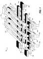
- FIG. 2an example of an imprint lithography mask 200 or template suitable for use in forming the memory lines 102 , 104 and vias 108 of the three-dimensional memory array shown in FIG. 1 is depicted.
- the imprint lithography mask 200 or templateis formed by etching a desired pattern into a translucent blank made from, for example, quartz or fused silica.
- the imprint mask 200includes interleaved rails 202 (corresponding to trenches) with wider landings 206 for forming contact pads at alternating ends of the rails 202 . Pillars 208 (corresponding to vias) project upwards from the top surface of each of the landings 206 .
- the imprint lithography mask 200may be formed at the minimum dimensions (e.g., line width and pitch) achievable by whichever technology (e.g., 32 nm, 16 nm, 9 nm photolithography, immersion lithography, etc.) may be used to pattern the mask 200 . Because a single mask 200 may be used repeatedly to form many layers of interconnect structures, the cost of manufacturing the mask 200 may be spread over each use of the mask 200 . Thus a net manufacturing cost reduction may be achieved by the methods and apparatus of the present invention.
- whichever technologye.g., 32 nm, 16 nm, 9 nm photolithography, immersion lithography, etc.
- the imprint lithography mask 200is inverted from the orientation shown and used to imprint its complement shape into a liquid transfer layer.
- the liquid transfer layeris then hardened or cured by exposure to light (e.g., ultraviolet) or other radiation transmitted directly through the translucent imprint lithography mask 200 .
- the hardened or cured transfer layermay be used during oxide etch to transfer the features of the imprint lithography mask 200 into a dielectric (e.g., oxide) layer.
- FIG. 3a second example of an imprint lithography mask 300 or template suitable for forming the memory lines and vias of a three-dimensional memory array is depicted.
- the simplified example mask 300corresponds to the mask 300 used in the processing sequence described below with respect to FIGS. 4 AX through 4 DX and 4 AY through 4 DY.
- FIGS. 4 AX, 4 BX, 4 CX, and 4 DXare cross-sectional views of a sequence of processing steps illustrating the formation of trenches and holes in a dielectric layer for use in manufacturing a memory array. As indicated in FIG.
- FIGS. 4 AY, 4 BY, 4 CY, and 4 DYare also cross-sectional views of the sequence of processing steps illustrating the formation of trenches and holes in the dielectric layer.
- the perspective of these viewsis looking across a trench and a via hole with the pillars of the imprint lithography mask 300 disposed on the left hand side of the cross-sectional views.
- the second example of an imprint lithography mask 300 or templatemay be formed by etching a desired pattern into a translucent blank made from, for example, quartz or fused silica.
- the imprint lithography mask 300may also be formed at the minimum dimensions (e.g., line width and pitch) achievable by whichever technology (e.g., 32 nm, 16 nm, 9 nm photolithography, immersion lithography, etc.) may be used to pattern the mask 300 .
- the cost of manufacturing the mask 300may be spread over each use of the mask 300 . Thus a net manufacturing cost reduction may be achieved by the methods and apparatus of the present invention.
- FIGS. 4 AX through 4 DX and 4 AY through 4 DYa method of forming memory lines and vias for a layer of a three-dimensional memory array is depicted from a front and side plan cross-sectional view, respectively.
- each side by side pair of drawingsrepresents a cross-sectional plan view of the same process step where the drawing numbers ending in X are views at the X-X cross-sectional cut line of FIG. 3 and the drawing numbers ending in Y are views at the Y-Y cross-sectional cut line of FIG. 3 , respectively.
- the inventive process of the present intentionmay begin with an initial arrangement of various material layers 402 - 408 selected to be suitable to form the desired devices in a memory array or other circuit.
- the imprint lithography mask 300is shown inserted in a transfer layer 402 .
- a hardmask layer 404has been deposited on a dielectric layer 406 which is on a conductor or wire layer 408 .
- the transfer layer 402facilitates concurrently transferring both the memory lines pattern and the vias pattern from the imprint lithography mask 300 to the dielectric layer 406 .
- transfer layer 402may be a photopolymerizable liquid material that is spin coated or otherwise deposited onto hardmask layer 404 .
- the transfer layer 402once cured, preferably provides high etch rate selectivity when subjected to subsequent etch processes that facilitate transfer of the desired dual damascene pattern.
- the transfer layer, 402may be resist or a conventional photoresist such as, for example, a spun on polymer PMMA and/or photo-curable materials such as those sold by Molecular Imprints Inc. under the name S-FIL Monomat Ac01, which may be cured by exposure to I-line radiation (e.g., 365 nanometers) utilizing a photo source such as 100 Watt Hg—Se ultraviolet arc lamp.
- a photo-curable materialthat may be utilized is a material that includes ethylene glycol diacrylate (3-acryloxypropyl)tris(trimethylsiloxy)silane, t-butyl acrylate, and 2-hydroxy-2-methyl-1-phenyl-propan-1-one. Other practicable materials may be used.
- the transfer layer 402may have an initial thickness in the range of approximately 500 angstroms to approximately 5,000 angstroms.
- a layer of hardmask material 404may be deposited.
- a polycrystalline semiconductor materialmay be used as a hardmask 404 such as polysilicon, a polycrystalline silicon-germanium alloy, polygermanium or any other suitable material.
- a materialsuch as tungsten (W) may be used.
- the hardmask material layer 404 thicknessmay be of varying thickness, depending on the etch process parameters used. In some embodiments, the hardmask material layer 404 may have an initial thickness in the range of approximately 500 angstroms to approximately 3000 angstroms.
- the dielectric layer 406is the layer into which the dual damascene interconnect structure is to ultimately be formed.
- Dielectric layer 406may include dielectric material or insulating material including silicon based dielectric materials, silicates, low k material, and the like.
- Silicon based dielectric materialsinclude silicon dioxide (SiO 2 ), silicon nitride, silicon oxynitride, and the like.
- Silicatesinclude fluorine doped silicon glass (FSG), tetraethylorthosilicate (TEOS), borophosphotetraethylorthosilicate (BPTEOS), phosphosilicate glass (PSG), borophosphosilicate glass (BPSG), and other suitable materials and spin-on glass (SOG).
- Low k polymer materialsinclude one or more of polyimides, fluorinated polyimides, polysilsequioxane, benzocyclobutene (BCB), poly(arylene ester), parylene F, parylene N, amorphous polytetrafluoroethylene, and the like.
- the dielectric layer 406may have an initial thickness in the range of approximately 1500 angstroms to approximately 10,000 angstroms.
- the conductive metal or wire layer 408may include tungsten (W) or any practicable conductor.
- the wire layer 408may have a thickness in the range of approximately 1000 angstroms to approximately 2000 angstroms.
- the wire layer 408may be formed on a substrate (not shown) and/or may be part of another memory level.
- the imprint lithography mask 300is depressed into transfer layer 402 .
- the transfer layer 402is then hardened by exposure to light (e.g., ultraviolet) or other radiation (e.g., an electron beam) transmitted directly through the translucent imprint lithography mask 300 .
- the mask 300is removed after the transfer layer 402 has been cured and a complementary version of the dual damascene features of the mask 300 remains.
- an etch processis applied to form the structure depicted in FIGS. 4 CX and 4 CY.
- the hardmask layer 404 that is exposed in the via holesis initially etched away. Then, during a partial etch of the dielectric layer 406 that was exposed in the via holes, the transfer layer 402 is eroded through to the hardmask layer 404 in the trench regions.
- the exposed area of hardmask layer 404 in the trenchesis etched away and the consequently exposed dielectric layer 406 is etched to form the final trenches.
- the area of the dielectric layer 406 in the via holes previously exposed,is etched away down to the wire layer 408 to form the final via holes.
- the remaining dielectric layer 406is then ready to receive a conductor material in the trenches and via holes.
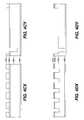
- FIGS. 5A through 5Dcross-sectional views of various different embodiments of columns of vias (referred to herein as zias) connecting adjacent word line layers and, if present, bit lines at different depths, are depicted.
- FIG. 5Adepicts horizontal word lines 502 connected by three stacked vias 508 forming a zia.
- the two depths labeled “a” and “b”correspond to the depths of the trenches and holes, respectively, formed by the rails and pillars, respectively, of an imprint lithography mask 300 .
- FIG. 5Balso depicts horizontal word lines 502 connected by stacked vias 508 forming a zia.
- a third damascene feature at a third depth “c”is included in the structure of FIG. 5B .
- This shoulder at a third depthallows connection to a bit line 504 running perpendicular (i.e., into and out of the page) to the word lines 502 as shown.
- FIG. 5Calso depicts horizontal word lines 502 connected by stacked vias 508 forming a zia and connections to bit lines 504 using a shoulder at an additional depth labeled “d.”
- depth dis deeper than depth c. This difference in the relative depths of the shoulders facilitates connection to features (e.g., bit lines) at different depths.
- FIG. 5Dincludes four depths of imprint a, b, c, d and connection to bit lines at two different depths are thus facilitated.
- FIG. 6depicts an example of an imprint lithography mask 600 that includes interleaved damascene features at four different depths a, b, c, d that could be used to facilitate making interconnections to bit lines 504 at two different depths c, d.
Landscapes
- Engineering & Computer Science (AREA)
- Physics & Mathematics (AREA)
- General Physics & Mathematics (AREA)
- Condensed Matter Physics & Semiconductors (AREA)
- Manufacturing & Machinery (AREA)
- Power Engineering (AREA)
- Computer Hardware Design (AREA)
- Microelectronics & Electronic Packaging (AREA)
- Nanotechnology (AREA)
- Chemical & Material Sciences (AREA)
- Crystallography & Structural Chemistry (AREA)
- Mathematical Physics (AREA)
- Theoretical Computer Science (AREA)
- Internal Circuitry In Semiconductor Integrated Circuit Devices (AREA)
- Semiconductor Memories (AREA)
- Non-Volatile Memory (AREA)
- Exposure Of Semiconductors, Excluding Electron Or Ion Beam Exposure (AREA)
- Shaping Of Tube Ends By Bending Or Straightening (AREA)
Abstract
Description
Claims (21)
Priority Applications (9)
| Application Number | Priority Date | Filing Date | Title |
|---|---|---|---|
| US11/967,638US8466068B2 (en) | 2007-12-31 | 2007-12-31 | Methods and apparatus for forming memory lines and vias in three dimensional memory arrays using dual damascene process and imprint lithography |
| KR1020107013806AKR20100120117A (en) | 2007-12-31 | 2008-12-31 | Methods and apparatus for forming memory lines and vias in three dimensional memory arrays using dual damascene process and imprint lithography |
| CN200880123672.4ACN101919046B (en) | 2007-12-31 | 2008-12-31 | Methods and apparatus for forming memory lines and vias in three dimensional memory arrays using dual damascene process and imprint lithography |
| TW097151904ATW200943491A (en) | 2007-12-31 | 2008-12-31 | Methods and apparatus for forming memory lines and vias in three dimensional memory arrays using dual damascene process and imprint lithography |
| PCT/US2008/088628WO2009088922A2 (en) | 2007-12-31 | 2008-12-31 | Methods and apparatus for forming memory lines and vias in three dimensional memory arrays using dual damascene process and imprint lithography |
| JP2010540951AJP2011508459A (en) | 2007-12-31 | 2008-12-31 | Method and apparatus for forming memory lines and vias in a three-dimensional memory array using dual damascene process and imprint lithography |
| EP08870141AEP2227823A4 (en) | 2007-12-31 | 2008-12-31 | METHODS AND APPARATUS FOR FORMING MEMORY LINES AND INTERCONNECTION HOLES IN THREE-DIMENSIONAL MEMORY ARRAYS USING DUAL DAMASCENE PROCESS AND PRINT LITHOGRAPHY |
| US12/856,392US20100301449A1 (en) | 2007-12-31 | 2010-08-13 | Methods and apparatus for forming line and pillar structures for three dimensional memory arrays using a double subtractive process and imprint lithography |
| US13/911,294US20130264675A1 (en) | 2007-12-31 | 2013-06-06 | Apparatus for forming memory lines and vias in three dimensional memory arrays using dual damascene process and imprint lithography |
Applications Claiming Priority (1)
| Application Number | Priority Date | Filing Date | Title |
|---|---|---|---|
| US11/967,638US8466068B2 (en) | 2007-12-31 | 2007-12-31 | Methods and apparatus for forming memory lines and vias in three dimensional memory arrays using dual damascene process and imprint lithography |
Related Child Applications (2)
| Application Number | Title | Priority Date | Filing Date |
|---|---|---|---|
| US12/856,392Continuation-In-PartUS20100301449A1 (en) | 2007-12-31 | 2010-08-13 | Methods and apparatus for forming line and pillar structures for three dimensional memory arrays using a double subtractive process and imprint lithography |
| US13/911,294DivisionUS20130264675A1 (en) | 2007-12-31 | 2013-06-06 | Apparatus for forming memory lines and vias in three dimensional memory arrays using dual damascene process and imprint lithography |
Publications (2)
| Publication Number | Publication Date |
|---|---|
| US20090166682A1 US20090166682A1 (en) | 2009-07-02 |
| US8466068B2true US8466068B2 (en) | 2013-06-18 |
Family
ID=40797036
Family Applications (2)
| Application Number | Title | Priority Date | Filing Date |
|---|---|---|---|
| US11/967,638Expired - Fee RelatedUS8466068B2 (en) | 2007-12-31 | 2007-12-31 | Methods and apparatus for forming memory lines and vias in three dimensional memory arrays using dual damascene process and imprint lithography |
| US13/911,294AbandonedUS20130264675A1 (en) | 2007-12-31 | 2013-06-06 | Apparatus for forming memory lines and vias in three dimensional memory arrays using dual damascene process and imprint lithography |
Family Applications After (1)
| Application Number | Title | Priority Date | Filing Date |
|---|---|---|---|
| US13/911,294AbandonedUS20130264675A1 (en) | 2007-12-31 | 2013-06-06 | Apparatus for forming memory lines and vias in three dimensional memory arrays using dual damascene process and imprint lithography |
Country Status (7)
| Country | Link |
|---|---|
| US (2) | US8466068B2 (en) |
| EP (1) | EP2227823A4 (en) |
| JP (1) | JP2011508459A (en) |
| KR (1) | KR20100120117A (en) |
| CN (1) | CN101919046B (en) |
| TW (1) | TW200943491A (en) |
| WO (1) | WO2009088922A2 (en) |
Cited By (5)
| Publication number | Priority date | Publication date | Assignee | Title |
|---|---|---|---|---|
| US10535669B2 (en)* | 2017-11-23 | 2020-01-14 | Yangtze Memory Technologies Co., Ltd. | Three-dimensional memory devices and fabricating methods thereof |
| US11800706B2 (en) | 2019-05-24 | 2023-10-24 | Micron Technology, Inc. | Integrated assemblies having conductive posts extending through stacks of alternating materials |
| US11806901B2 (en) | 2020-09-17 | 2023-11-07 | Kioxia Corporation | Template, template manufacturing method, and semiconductor device manufacturing method |
| US11869866B2 (en) | 2020-03-12 | 2024-01-09 | Kioxia Corporation | Wiring formation method, method for manufacturing semiconductor device, and semiconductor device |
| US12204251B2 (en) | 2021-03-23 | 2025-01-21 | Kioxia Corporation | Pattern generation method, template, and method for manufacturing template |
Families Citing this family (22)
| Publication number | Priority date | Publication date | Assignee | Title |
|---|---|---|---|---|
| KR100944605B1 (en)* | 2007-12-24 | 2010-02-25 | 주식회사 동부하이텍 | Semiconductor device |
| US20100301449A1 (en)* | 2007-12-31 | 2010-12-02 | Sandisk 3D Llc | Methods and apparatus for forming line and pillar structures for three dimensional memory arrays using a double subtractive process and imprint lithography |
| US8466068B2 (en) | 2007-12-31 | 2013-06-18 | Sandisk 3D Llc | Methods and apparatus for forming memory lines and vias in three dimensional memory arrays using dual damascene process and imprint lithography |
| JP4945609B2 (en)* | 2009-09-02 | 2012-06-06 | 株式会社東芝 | Semiconductor integrated circuit device |
| KR20120089697A (en)* | 2009-10-26 | 2012-08-13 | 쌘디스크 3디 엘엘씨 | Apparatus and methods of forming memory lines and structures using double sidewall patterning for four times half pitch relief patterning |
| CN103493201B (en)* | 2011-03-29 | 2016-04-13 | 惠普发展公司,有限责任合伙企业 | Dual-plane memory array |
| US9230611B2 (en) | 2011-11-04 | 2016-01-05 | Hewlett Packard Enterprise Development Lp | Structure of a switching device in an array |
| US20140353019A1 (en)* | 2013-05-30 | 2014-12-04 | Deepak ARORA | Formation of dielectric with smooth surface |
| US9728584B2 (en) | 2013-06-11 | 2017-08-08 | Micron Technology, Inc. | Three dimensional memory array with select device |
| TWI562281B (en)* | 2015-08-07 | 2016-12-11 | Macronix Int Co Ltd | Memory device and method of manufacturing the same |
| KR102449571B1 (en)* | 2015-08-07 | 2022-10-04 | 삼성전자주식회사 | Semiconductor Device |
| US9812502B2 (en) | 2015-08-31 | 2017-11-07 | Toshiba Memory Corporation | Semiconductor memory device having variable resistance elements provided at intersections of wiring lines |
| KR102475454B1 (en) | 2016-01-08 | 2022-12-08 | 에스케이하이닉스 주식회사 | Semiconductor device and manufacturing method of the same |
| US10354912B2 (en)* | 2016-03-21 | 2019-07-16 | Qualcomm Incorporated | Forming self-aligned vertical interconnect accesses (VIAs) in interconnect structures for integrated circuits (ICs) |
| KR102673120B1 (en)* | 2016-12-05 | 2024-06-05 | 삼성전자주식회사 | Semiconductor device and method for fabricating the same |
| WO2018148659A1 (en)* | 2017-02-10 | 2018-08-16 | Northeastern University | Damascene template for nanoelement printing fabricated without chemomechanical planarizaton |
| CN107946237A (en)* | 2017-11-23 | 2018-04-20 | 长江存储科技有限责任公司 | Three-dimensional storage organization bus connection method, storage organization, memory and electronic equipment |
| CN110391242B (en)* | 2019-07-31 | 2021-08-20 | 中国科学院微电子研究所 | L-shaped stepped word line structure, method for fabricating the same, and three-dimensional memory |
| JP2021141252A (en)* | 2020-03-06 | 2021-09-16 | キオクシア株式会社 | Semiconductor devices and their manufacturing methods |
| JP7458948B2 (en)* | 2020-09-17 | 2024-04-01 | キオクシア株式会社 | Template, template manufacturing method, and semiconductor device manufacturing method |
| JP2022076684A (en)* | 2020-11-10 | 2022-05-20 | ソニーセミコンダクタソリューションズ株式会社 | Semiconductor device |
| JP2022142518A (en) | 2021-03-16 | 2022-09-30 | キオクシア株式会社 | TEMPLATE, MARK AND METHOD FOR MANUFACTURE OF TEMPLATE |
Citations (34)
| Publication number | Priority date | Publication date | Assignee | Title |
|---|---|---|---|---|
| WO2001020402A1 (en) | 1999-09-14 | 2001-03-22 | Massachusetts Institute Of Technology | Fabrication of finely featured devices by liquid embossing |
| US20010050385A1 (en)* | 1999-04-28 | 2001-12-13 | Kotecki David E. | Method for simultaneously forming a storage-capacitor electrode and interconnect |
| US20020088998A1 (en) | 2000-04-28 | 2002-07-11 | Knall N. Johan | Three-dimensional memory array and method of fabrication |
| US6515888B2 (en) | 2000-08-14 | 2003-02-04 | Matrix Semiconductor, Inc. | Low cost three-dimensional memory array |
| US6534403B2 (en) | 2000-12-22 | 2003-03-18 | Matrix Semiconductor | Method of making a contact and via structure |
| WO2003030252A2 (en) | 2001-09-28 | 2003-04-10 | Hrl Laboratories, Llc | Process for producing interconnects |
| EP1387216A2 (en) | 2002-08-01 | 2004-02-04 | Hitachi, Ltd. | Stamper, lithographic method of using the stamper and method of forming a structure by a lithographic pattern |
| CN1487362A (en) | 2002-09-17 | 2004-04-07 | ��������˹�����տ����� | Impression mask photoetching |
| US6822903B2 (en) | 2003-03-31 | 2004-11-23 | Matrix Semiconductor, Inc. | Apparatus and method for disturb-free programming of passive element memory cells |
| US20040245547A1 (en) | 2003-06-03 | 2004-12-09 | Hitachi Global Storage Technologies B.V. | Ultra low-cost solid-state memory |
| US20050062165A1 (en) | 2003-09-19 | 2005-03-24 | International Business Machines Corporation | Method of forming closed air gap interconnects and structures formed thereby |
| US20050170269A1 (en) | 2003-06-20 | 2005-08-04 | Matsushita Electric Industrial Co., Ltd. | Pattern formation method and method for forming semiconductor device |
| US6951780B1 (en) | 2003-12-18 | 2005-10-04 | Matrix Semiconductor, Inc. | Selective oxidation of silicon in diode, TFT, and monolithic three dimensional memory arrays |
| CN1791967A (en) | 2003-04-25 | 2006-06-21 | 分子制模股份有限公司 | A method of forming stepped structures employing imprint lithography |
| US7091084B2 (en) | 2002-09-20 | 2006-08-15 | Intel Corporation | Ultra-high capacitance device based on nanostructures |
| US20060240681A1 (en) | 2005-04-25 | 2006-10-26 | Williams R S | Three-dimensional nanoscale crossbars |
| US7148142B1 (en)* | 2004-06-23 | 2006-12-12 | Advanced Micro Devices, Inc. | System and method for imprint lithography to facilitate dual damascene integration in a single imprint act |
| US7195950B2 (en) | 2004-07-21 | 2007-03-27 | Hewlett-Packard Development Company, L.P. | Forming a plurality of thin-film devices |
| EP1796159A2 (en) | 2005-12-07 | 2007-06-13 | Canon Kabushiki Kaisha | Method for manufacturing a semiconductor device by using a dual damascene process |
| US7256435B1 (en) | 2003-06-02 | 2007-08-14 | Hewlett-Packard Development Company, L.P. | Multilevel imprint lithography |
| US20070210449A1 (en) | 2006-03-07 | 2007-09-13 | Dirk Caspary | Memory device and an array of conductive lines and methods of making the same |
| US20070281219A1 (en) | 2006-06-01 | 2007-12-06 | Sandhu Gurtej S | Masking techniques and contact imprint reticles for dense semiconductor fabrication |
| US7396465B2 (en)* | 1999-02-25 | 2008-07-08 | Pall Corporation | Positively charged membrane |
| US20080167396A1 (en) | 2006-10-16 | 2008-07-10 | Kenji Murao | Fine Resinous Structure, Fabrication Thereof, and Polymerizable Resin-Precursor Composition |
| US7410904B2 (en)* | 2003-04-24 | 2008-08-12 | Hewlett-Packard Development Company, L.P. | Sensor produced using imprint lithography |
| US7462292B2 (en)* | 2004-01-27 | 2008-12-09 | Hewlett-Packard Development Company, L.P. | Silicon carbide imprint stamp |
| US7474000B2 (en) | 2003-12-05 | 2009-01-06 | Sandisk 3D Llc | High density contact to relaxed geometry layers |
| US7505321B2 (en) | 2002-12-31 | 2009-03-17 | Sandisk 3D Llc | Programmable memory array structure incorporating series-connected transistor strings and methods for fabrication and operation of same |
| US7508714B2 (en) | 2003-12-05 | 2009-03-24 | Sandisk 3D Llc | Memory array incorporating mirrored NAND strings and non-shared global bit lines within a block |
| US20090166682A1 (en) | 2007-12-31 | 2009-07-02 | Scheuerlein Roy E | Methods and apparatus for forming memory lines and vias in three dimensional memory arrays using dual damascene process and imprint lithography |
| WO2010041302A1 (en) | 2008-10-06 | 2010-04-15 | 株式会社 東芝 | Variable resistance memory |
| US20100301449A1 (en) | 2007-12-31 | 2010-12-02 | Sandisk 3D Llc | Methods and apparatus for forming line and pillar structures for three dimensional memory arrays using a double subtractive process and imprint lithography |
| US7928004B2 (en)* | 2006-06-30 | 2011-04-19 | Advanced Micro Devices, Inc. | Nano imprint technique with increased flexibility with respect to alignment and feature shaping |
| US8003310B2 (en) | 2006-04-24 | 2011-08-23 | Micron Technology, Inc. | Masking techniques and templates for dense semiconductor fabrication |
Family Cites Families (3)
| Publication number | Priority date | Publication date | Assignee | Title |
|---|---|---|---|---|
| US3723790A (en)* | 1971-02-01 | 1973-03-27 | Corning Glass Works | Electrical lamp or tube comprising copper coated nickel-iron alloy electrical current conductors and a glass enclosure |
| US6124224A (en)* | 1998-09-02 | 2000-09-26 | Ferro Corporation | High temperature sealing glass |
| US20080023885A1 (en)* | 2006-06-15 | 2008-01-31 | Nanochip, Inc. | Method for forming a nano-imprint lithography template having very high feature counts |
- 2007
- 2007-12-31USUS11/967,638patent/US8466068B2/ennot_activeExpired - Fee Related
- 2008
- 2008-12-31EPEP08870141Apatent/EP2227823A4/ennot_activeWithdrawn
- 2008-12-31TWTW097151904Apatent/TW200943491A/enunknown
- 2008-12-31WOPCT/US2008/088628patent/WO2009088922A2/enactiveApplication Filing
- 2008-12-31CNCN200880123672.4Apatent/CN101919046B/ennot_activeExpired - Fee Related
- 2008-12-31JPJP2010540951Apatent/JP2011508459A/enactivePending
- 2008-12-31KRKR1020107013806Apatent/KR20100120117A/ennot_activeWithdrawn
- 2013
- 2013-06-06USUS13/911,294patent/US20130264675A1/ennot_activeAbandoned
Patent Citations (42)
| Publication number | Priority date | Publication date | Assignee | Title |
|---|---|---|---|---|
| US7396465B2 (en)* | 1999-02-25 | 2008-07-08 | Pall Corporation | Positively charged membrane |
| US20010050385A1 (en)* | 1999-04-28 | 2001-12-13 | Kotecki David E. | Method for simultaneously forming a storage-capacitor electrode and interconnect |
| WO2001020402A1 (en) | 1999-09-14 | 2001-03-22 | Massachusetts Institute Of Technology | Fabrication of finely featured devices by liquid embossing |
| US20020088998A1 (en) | 2000-04-28 | 2002-07-11 | Knall N. Johan | Three-dimensional memory array and method of fabrication |
| US6420215B1 (en) | 2000-04-28 | 2002-07-16 | Matrix Semiconductor, Inc. | Three-dimensional memory array and method of fabrication |
| US6515888B2 (en) | 2000-08-14 | 2003-02-04 | Matrix Semiconductor, Inc. | Low cost three-dimensional memory array |
| US6534403B2 (en) | 2000-12-22 | 2003-03-18 | Matrix Semiconductor | Method of making a contact and via structure |
| WO2003030252A2 (en) | 2001-09-28 | 2003-04-10 | Hrl Laboratories, Llc | Process for producing interconnects |
| EP1387216A2 (en) | 2002-08-01 | 2004-02-04 | Hitachi, Ltd. | Stamper, lithographic method of using the stamper and method of forming a structure by a lithographic pattern |
| KR20040012563A (en) | 2002-08-01 | 2004-02-11 | 가부시끼가이샤 히다치 세이사꾸쇼 | Stamper, pattern transcription method using therewith and forming structure by transcripted pattern |
| CN1487362A (en) | 2002-09-17 | 2004-04-07 | ��������˹�����տ����� | Impression mask photoetching |
| US7091084B2 (en) | 2002-09-20 | 2006-08-15 | Intel Corporation | Ultra-high capacitance device based on nanostructures |
| US7505321B2 (en) | 2002-12-31 | 2009-03-17 | Sandisk 3D Llc | Programmable memory array structure incorporating series-connected transistor strings and methods for fabrication and operation of same |
| US6822903B2 (en) | 2003-03-31 | 2004-11-23 | Matrix Semiconductor, Inc. | Apparatus and method for disturb-free programming of passive element memory cells |
| US6963504B2 (en) | 2003-03-31 | 2005-11-08 | Matrix Semiconductor, Inc. | Apparatus and method for disturb-free programming of passive element memory cells |
| US7410904B2 (en)* | 2003-04-24 | 2008-08-12 | Hewlett-Packard Development Company, L.P. | Sensor produced using imprint lithography |
| US7396475B2 (en)* | 2003-04-25 | 2008-07-08 | Molecular Imprints, Inc. | Method of forming stepped structures employing imprint lithography |
| CN1791967A (en) | 2003-04-25 | 2006-06-21 | 分子制模股份有限公司 | A method of forming stepped structures employing imprint lithography |
| US7256435B1 (en) | 2003-06-02 | 2007-08-14 | Hewlett-Packard Development Company, L.P. | Multilevel imprint lithography |
| US20040245547A1 (en) | 2003-06-03 | 2004-12-09 | Hitachi Global Storage Technologies B.V. | Ultra low-cost solid-state memory |
| CN1698181A (en) | 2003-06-20 | 2005-11-16 | 松下电器产业株式会社 | Pattern forming method and method of manufacturing semiconductor device |
| US20050170269A1 (en) | 2003-06-20 | 2005-08-04 | Matsushita Electric Industrial Co., Ltd. | Pattern formation method and method for forming semiconductor device |
| US20050062165A1 (en) | 2003-09-19 | 2005-03-24 | International Business Machines Corporation | Method of forming closed air gap interconnects and structures formed thereby |
| US7508714B2 (en) | 2003-12-05 | 2009-03-24 | Sandisk 3D Llc | Memory array incorporating mirrored NAND strings and non-shared global bit lines within a block |
| US7474000B2 (en) | 2003-12-05 | 2009-01-06 | Sandisk 3D Llc | High density contact to relaxed geometry layers |
| US6951780B1 (en) | 2003-12-18 | 2005-10-04 | Matrix Semiconductor, Inc. | Selective oxidation of silicon in diode, TFT, and monolithic three dimensional memory arrays |
| US7462292B2 (en)* | 2004-01-27 | 2008-12-09 | Hewlett-Packard Development Company, L.P. | Silicon carbide imprint stamp |
| US7148142B1 (en)* | 2004-06-23 | 2006-12-12 | Advanced Micro Devices, Inc. | System and method for imprint lithography to facilitate dual damascene integration in a single imprint act |
| US7195950B2 (en) | 2004-07-21 | 2007-03-27 | Hewlett-Packard Development Company, L.P. | Forming a plurality of thin-film devices |
| US20060240681A1 (en) | 2005-04-25 | 2006-10-26 | Williams R S | Three-dimensional nanoscale crossbars |
| EP1796159A2 (en) | 2005-12-07 | 2007-06-13 | Canon Kabushiki Kaisha | Method for manufacturing a semiconductor device by using a dual damascene process |
| US20070210449A1 (en) | 2006-03-07 | 2007-09-13 | Dirk Caspary | Memory device and an array of conductive lines and methods of making the same |
| US8003310B2 (en) | 2006-04-24 | 2011-08-23 | Micron Technology, Inc. | Masking techniques and templates for dense semiconductor fabrication |
| US20070281219A1 (en) | 2006-06-01 | 2007-12-06 | Sandhu Gurtej S | Masking techniques and contact imprint reticles for dense semiconductor fabrication |
| US7795149B2 (en)* | 2006-06-01 | 2010-09-14 | Micron Technology, Inc. | Masking techniques and contact imprint reticles for dense semiconductor fabrication |
| US7928004B2 (en)* | 2006-06-30 | 2011-04-19 | Advanced Micro Devices, Inc. | Nano imprint technique with increased flexibility with respect to alignment and feature shaping |
| US20080167396A1 (en) | 2006-10-16 | 2008-07-10 | Kenji Murao | Fine Resinous Structure, Fabrication Thereof, and Polymerizable Resin-Precursor Composition |
| US7883764B2 (en) | 2006-10-16 | 2011-02-08 | Hitachi Chemical Company, Ltd. | Fine resinous structure, fabrication thereof, and polymerizable resin-precursor composition |
| US20090166682A1 (en) | 2007-12-31 | 2009-07-02 | Scheuerlein Roy E | Methods and apparatus for forming memory lines and vias in three dimensional memory arrays using dual damascene process and imprint lithography |
| US20100301449A1 (en) | 2007-12-31 | 2010-12-02 | Sandisk 3D Llc | Methods and apparatus for forming line and pillar structures for three dimensional memory arrays using a double subtractive process and imprint lithography |
| WO2010041302A1 (en) | 2008-10-06 | 2010-04-15 | 株式会社 東芝 | Variable resistance memory |
| US20110228589A1 (en) | 2008-10-06 | 2011-09-22 | Kenichi Murooka | Resistance change memory |
Non-Patent Citations (7)
| Title |
|---|
| Apr. 15, 2013 Reply to Jan. 30, 2013 Office Action of counterpart Chinese Patent Application No. 200880123672.4. |
| Communication pursuant to Rules 70(2) and 70a(2) EPC of counterpart European Patent Application No. 08870141.2 mailed Apr. 5, 2012. |
| Extended Search Report of counterpart European Patent Application No. 08870141.2 mailed Mar. 19, 2012. |
| First Office Action and Search Report of counterpart Chinese Patent Application No. 200880123672.4 mailed Jun. 26, 2012. |
| International Search Report and Written Opinion of International Application No. PCT/US2008/088628 mailed Jul. 29, 2009. |
| Oct. 24, 2012 Response to Jun. 26, 2012 Office Action and Search Report of counterpart Chinese Patent Application No. 200880123672.4. |
| Office Action of counterpart Chinese Patent Application No. 200880123672.4 dated Jan. 30, 2013. |
Cited By (6)
| Publication number | Priority date | Publication date | Assignee | Title |
|---|---|---|---|---|
| US10535669B2 (en)* | 2017-11-23 | 2020-01-14 | Yangtze Memory Technologies Co., Ltd. | Three-dimensional memory devices and fabricating methods thereof |
| US10770468B2 (en) | 2017-11-23 | 2020-09-08 | Yangtze Memory Technologies Co., Ltd. | Three-dimensional memory devices and fabricating methods thereof |
| US11800706B2 (en) | 2019-05-24 | 2023-10-24 | Micron Technology, Inc. | Integrated assemblies having conductive posts extending through stacks of alternating materials |
| US11869866B2 (en) | 2020-03-12 | 2024-01-09 | Kioxia Corporation | Wiring formation method, method for manufacturing semiconductor device, and semiconductor device |
| US11806901B2 (en) | 2020-09-17 | 2023-11-07 | Kioxia Corporation | Template, template manufacturing method, and semiconductor device manufacturing method |
| US12204251B2 (en) | 2021-03-23 | 2025-01-21 | Kioxia Corporation | Pattern generation method, template, and method for manufacturing template |
Also Published As
| Publication number | Publication date |
|---|---|
| WO2009088922A2 (en) | 2009-07-16 |
| CN101919046A (en) | 2010-12-15 |
| JP2011508459A (en) | 2011-03-10 |
| CN101919046B (en) | 2013-11-06 |
| EP2227823A4 (en) | 2012-04-18 |
| TW200943491A (en) | 2009-10-16 |
| EP2227823A2 (en) | 2010-09-15 |
| US20090166682A1 (en) | 2009-07-02 |
| WO2009088922A3 (en) | 2009-09-24 |
| KR20100120117A (en) | 2010-11-12 |
| US20130264675A1 (en) | 2013-10-10 |
Similar Documents
| Publication | Publication Date | Title |
|---|---|---|
| US8466068B2 (en) | Methods and apparatus for forming memory lines and vias in three dimensional memory arrays using dual damascene process and imprint lithography | |
| US10957582B2 (en) | Self aligned via and pillar cut for at least a self aligned double pitch | |
| US20100301449A1 (en) | Methods and apparatus for forming line and pillar structures for three dimensional memory arrays using a double subtractive process and imprint lithography | |
| US9263391B2 (en) | Interconnect structures incorporating air-gap spacers | |
| US10600678B2 (en) | Self-aligned isotropic etch of pre-formed vias and plugs for back end of line (BEOL) interconnects | |
| JP7348441B2 (en) | Subtractive interconnect formation using fully self-aligned method | |
| CN110660732A (en) | Method for forming integrated circuit device | |
| CN108074799B (en) | Method of forming semiconductor device using semi-bidirectional patterning | |
| US8716133B2 (en) | Three photomask sidewall image transfer method | |
| CN1514478A (en) | Robust ultra-low-k interconnect structure utilizing bridge-first metallization fabrication sequence | |
| CN108074808B (en) | Method of forming semiconductor device using semi-bidirectional patterning and islands | |
| JP4104426B2 (en) | Manufacturing method of semiconductor device | |
| KR101981867B1 (en) | Semiconductor device and manufacturing method thereof | |
| CN110718451B (en) | Method for manufacturing semiconductor structure | |
| US20240355633A1 (en) | Processes for reducing line-end spacing | |
| CN107204279B (en) | Method of forming semiconductor device | |
| US20090087993A1 (en) | Methods and apparatus for cost-effectively increasing feature density using a mask shrinking process with double patterning | |
| CN103531528A (en) | Method for manufacturing dual damascene structure | |
| JP6140616B2 (en) | Pattern division decomposition strategy for double patterned lithography process | |
| US12293970B2 (en) | Semiconductor structure and method for manufacturing thereof | |
| US20230096938A1 (en) | Fabrication of back-end-of-line interconnects | |
| JP4684984B2 (en) | Semiconductor device manufacturing method and article manufacturing method |
Legal Events
| Date | Code | Title | Description |
|---|---|---|---|
| AS | Assignment | Owner name:SANDISK 3D LLC, CALIFORNIA Free format text:ASSIGNMENT OF ASSIGNORS INTEREST;ASSIGNOR:SCHEUERLEIN, ROY E.;REEL/FRAME:020610/0779 Effective date:20080221 | |
| STCF | Information on status: patent grant | Free format text:PATENTED CASE | |
| AS | Assignment | Owner name:SANDISK TECHNOLOGIES INC., TEXAS Free format text:ASSIGNMENT OF ASSIGNORS INTEREST;ASSIGNOR:SANDISK 3D LLC.;REEL/FRAME:038300/0665 Effective date:20160324 | |
| AS | Assignment | Owner name:SANDISK TECHNOLOGIES INC., TEXAS Free format text:CORRECTIVE ASSIGNMENT TO CORRECT THE INCORRECT LISTED PATENT NUMBER 8853569 TO THE CORRECT PATENT NUMBER 8883569 PREVIOUSLY RECORDED ON REEL 038300 FRAME 0665. ASSIGNOR(S) HEREBY CONFIRMS THE ASSIGNMENT;ASSIGNOR:SANDISK 3D LLC;REEL/FRAME:038520/0552 Effective date:20160324 | |
| AS | Assignment | Owner name:SANDISK TECHNOLOGIES LLC, TEXAS Free format text:CHANGE OF NAME;ASSIGNOR:SANDISK TECHNOLOGIES INC;REEL/FRAME:038809/0600 Effective date:20160516 | |
| FPAY | Fee payment | Year of fee payment:4 | |
| FEPP | Fee payment procedure | Free format text:MAINTENANCE FEE REMINDER MAILED (ORIGINAL EVENT CODE: REM.); ENTITY STATUS OF PATENT OWNER: LARGE ENTITY | |
| LAPS | Lapse for failure to pay maintenance fees | Free format text:PATENT EXPIRED FOR FAILURE TO PAY MAINTENANCE FEES (ORIGINAL EVENT CODE: EXP.); ENTITY STATUS OF PATENT OWNER: LARGE ENTITY | |
| STCH | Information on status: patent discontinuation | Free format text:PATENT EXPIRED DUE TO NONPAYMENT OF MAINTENANCE FEES UNDER 37 CFR 1.362 | |
| FP | Lapsed due to failure to pay maintenance fee | Effective date:20210618 | |
| AS | Assignment | Owner name:WODEN TECHNOLOGIES INC., DELAWARE Free format text:ASSIGNMENT OF ASSIGNORS INTEREST;ASSIGNOR:SANDISK TECHNOLOGIES LLC;REEL/FRAME:058871/0928 Effective date:20210729 |