US8466016B2 - Hafnium tantalum oxynitride dielectric - Google Patents
Hafnium tantalum oxynitride dielectricDownload PDFInfo
- Publication number
- US8466016B2 US8466016B2US13/332,222US201113332222AUS8466016B2US 8466016 B2US8466016 B2US 8466016B2US 201113332222 AUS201113332222 AUS 201113332222AUS 8466016 B2US8466016 B2US 8466016B2
- Authority
- US
- United States
- Prior art keywords
- layer
- forming
- dielectric
- metal
- precursor
- Prior art date
- Legal status (The legal status is an assumption and is not a legal conclusion. Google has not performed a legal analysis and makes no representation as to the accuracy of the status listed.)
- Active
Links
Images


Classifications
- H—ELECTRICITY
- H10—SEMICONDUCTOR DEVICES; ELECTRIC SOLID-STATE DEVICES NOT OTHERWISE PROVIDED FOR
- H10D—INORGANIC ELECTRIC SEMICONDUCTOR DEVICES
- H10D64/00—Electrodes of devices having potential barriers
- H10D64/01—Manufacture or treatment
- H10D64/015—Manufacture or treatment removing at least parts of gate spacers, e.g. disposable spacers
- G—PHYSICS
- G11—INFORMATION STORAGE
- G11C—STATIC STORES
- G11C16/00—Erasable programmable read-only memories
- G11C16/02—Erasable programmable read-only memories electrically programmable
- G11C16/04—Erasable programmable read-only memories electrically programmable using variable threshold transistors, e.g. FAMOS
- G11C16/0466—Erasable programmable read-only memories electrically programmable using variable threshold transistors, e.g. FAMOS comprising cells with charge storage in an insulating layer, e.g. metal-nitride-oxide-silicon [MNOS], silicon-oxide-nitride-oxide-silicon [SONOS]
- H—ELECTRICITY
- H01—ELECTRIC ELEMENTS
- H01L—SEMICONDUCTOR DEVICES NOT COVERED BY CLASS H10
- H01L21/00—Processes or apparatus adapted for the manufacture or treatment of semiconductor or solid state devices or of parts thereof
- H01L21/02—Manufacture or treatment of semiconductor devices or of parts thereof
- H01L21/02104—Forming layers
- H01L21/02107—Forming insulating materials on a substrate
- H01L21/02109—Forming insulating materials on a substrate characterised by the type of layer, e.g. type of material, porous/non-porous, pre-cursors, mixtures or laminates
- H01L21/02112—Forming insulating materials on a substrate characterised by the type of layer, e.g. type of material, porous/non-porous, pre-cursors, mixtures or laminates characterised by the material of the layer
- H01L21/02172—Forming insulating materials on a substrate characterised by the type of layer, e.g. type of material, porous/non-porous, pre-cursors, mixtures or laminates characterised by the material of the layer the material containing at least one metal element, e.g. metal oxides, metal nitrides, metal oxynitrides or metal carbides
- H01L21/02175—Forming insulating materials on a substrate characterised by the type of layer, e.g. type of material, porous/non-porous, pre-cursors, mixtures or laminates characterised by the material of the layer the material containing at least one metal element, e.g. metal oxides, metal nitrides, metal oxynitrides or metal carbides characterised by the metal
- H01L21/02183—Forming insulating materials on a substrate characterised by the type of layer, e.g. type of material, porous/non-porous, pre-cursors, mixtures or laminates characterised by the material of the layer the material containing at least one metal element, e.g. metal oxides, metal nitrides, metal oxynitrides or metal carbides characterised by the metal the material containing tantalum, e.g. Ta2O5
- H—ELECTRICITY
- H01—ELECTRIC ELEMENTS
- H01L—SEMICONDUCTOR DEVICES NOT COVERED BY CLASS H10
- H01L21/00—Processes or apparatus adapted for the manufacture or treatment of semiconductor or solid state devices or of parts thereof
- H01L21/02—Manufacture or treatment of semiconductor devices or of parts thereof
- H01L21/02104—Forming layers
- H01L21/02107—Forming insulating materials on a substrate
- H01L21/02109—Forming insulating materials on a substrate characterised by the type of layer, e.g. type of material, porous/non-porous, pre-cursors, mixtures or laminates
- H01L21/02205—Forming insulating materials on a substrate characterised by the type of layer, e.g. type of material, porous/non-porous, pre-cursors, mixtures or laminates the layer being characterised by the precursor material for deposition
- H01L21/02208—Forming insulating materials on a substrate characterised by the type of layer, e.g. type of material, porous/non-porous, pre-cursors, mixtures or laminates the layer being characterised by the precursor material for deposition the precursor containing a compound comprising Si
- H01L21/02219—Forming insulating materials on a substrate characterised by the type of layer, e.g. type of material, porous/non-porous, pre-cursors, mixtures or laminates the layer being characterised by the precursor material for deposition the precursor containing a compound comprising Si the compound comprising silicon and nitrogen
- H01L21/02222—Forming insulating materials on a substrate characterised by the type of layer, e.g. type of material, porous/non-porous, pre-cursors, mixtures or laminates the layer being characterised by the precursor material for deposition the precursor containing a compound comprising Si the compound comprising silicon and nitrogen the compound being a silazane
- H—ELECTRICITY
- H10—SEMICONDUCTOR DEVICES; ELECTRIC SOLID-STATE DEVICES NOT OTHERWISE PROVIDED FOR
- H10D—INORGANIC ELECTRIC SEMICONDUCTOR DEVICES
- H10D64/00—Electrodes of devices having potential barriers
- H10D64/01—Manufacture or treatment
- H10D64/017—Manufacture or treatment using dummy gates in processes wherein at least parts of the final gates are self-aligned to the dummy gates, i.e. replacement gate processes
- H—ELECTRICITY
- H10—SEMICONDUCTOR DEVICES; ELECTRIC SOLID-STATE DEVICES NOT OTHERWISE PROVIDED FOR
- H10D—INORGANIC ELECTRIC SEMICONDUCTOR DEVICES
- H10D64/00—Electrodes of devices having potential barriers
- H10D64/60—Electrodes characterised by their materials
- H10D64/66—Electrodes having a conductor capacitively coupled to a semiconductor by an insulator, e.g. MIS electrodes
- H10D64/68—Electrodes having a conductor capacitively coupled to a semiconductor by an insulator, e.g. MIS electrodes characterised by the insulator, e.g. by the gate insulator
- H10D64/691—Electrodes having a conductor capacitively coupled to a semiconductor by an insulator, e.g. MIS electrodes characterised by the insulator, e.g. by the gate insulator comprising metallic compounds, e.g. metal oxides or metal silicates
- H—ELECTRICITY
- H10—SEMICONDUCTOR DEVICES; ELECTRIC SOLID-STATE DEVICES NOT OTHERWISE PROVIDED FOR
- H10D—INORGANIC ELECTRIC SEMICONDUCTOR DEVICES
- H10D64/00—Electrodes of devices having potential barriers
- H10D64/60—Electrodes characterised by their materials
- H10D64/66—Electrodes having a conductor capacitively coupled to a semiconductor by an insulator, e.g. MIS electrodes
- H10D64/68—Electrodes having a conductor capacitively coupled to a semiconductor by an insulator, e.g. MIS electrodes characterised by the insulator, e.g. by the gate insulator
- H10D64/693—Electrodes having a conductor capacitively coupled to a semiconductor by an insulator, e.g. MIS electrodes characterised by the insulator, e.g. by the gate insulator the insulator comprising nitrogen, e.g. nitrides, oxynitrides or nitrogen-doped materials
- H—ELECTRICITY
- H01—ELECTRIC ELEMENTS
- H01L—SEMICONDUCTOR DEVICES NOT COVERED BY CLASS H10
- H01L21/00—Processes or apparatus adapted for the manufacture or treatment of semiconductor or solid state devices or of parts thereof
- H01L21/02—Manufacture or treatment of semiconductor devices or of parts thereof
- H01L21/02104—Forming layers
- H01L21/02107—Forming insulating materials on a substrate
- H01L21/02109—Forming insulating materials on a substrate characterised by the type of layer, e.g. type of material, porous/non-porous, pre-cursors, mixtures or laminates
- H01L21/02112—Forming insulating materials on a substrate characterised by the type of layer, e.g. type of material, porous/non-porous, pre-cursors, mixtures or laminates characterised by the material of the layer
- H01L21/02172—Forming insulating materials on a substrate characterised by the type of layer, e.g. type of material, porous/non-porous, pre-cursors, mixtures or laminates characterised by the material of the layer the material containing at least one metal element, e.g. metal oxides, metal nitrides, metal oxynitrides or metal carbides
- H01L21/02175—Forming insulating materials on a substrate characterised by the type of layer, e.g. type of material, porous/non-porous, pre-cursors, mixtures or laminates characterised by the material of the layer the material containing at least one metal element, e.g. metal oxides, metal nitrides, metal oxynitrides or metal carbides characterised by the metal
- H01L21/02181—Forming insulating materials on a substrate characterised by the type of layer, e.g. type of material, porous/non-porous, pre-cursors, mixtures or laminates characterised by the material of the layer the material containing at least one metal element, e.g. metal oxides, metal nitrides, metal oxynitrides or metal carbides characterised by the metal the material containing hafnium, e.g. HfO2
- H—ELECTRICITY
- H01—ELECTRIC ELEMENTS
- H01L—SEMICONDUCTOR DEVICES NOT COVERED BY CLASS H10
- H01L21/00—Processes or apparatus adapted for the manufacture or treatment of semiconductor or solid state devices or of parts thereof
- H01L21/02—Manufacture or treatment of semiconductor devices or of parts thereof
- H01L21/02104—Forming layers
- H01L21/02107—Forming insulating materials on a substrate
- H01L21/02109—Forming insulating materials on a substrate characterised by the type of layer, e.g. type of material, porous/non-porous, pre-cursors, mixtures or laminates
- H01L21/02112—Forming insulating materials on a substrate characterised by the type of layer, e.g. type of material, porous/non-porous, pre-cursors, mixtures or laminates characterised by the material of the layer
- H01L21/02172—Forming insulating materials on a substrate characterised by the type of layer, e.g. type of material, porous/non-porous, pre-cursors, mixtures or laminates characterised by the material of the layer the material containing at least one metal element, e.g. metal oxides, metal nitrides, metal oxynitrides or metal carbides
- H01L21/02175—Forming insulating materials on a substrate characterised by the type of layer, e.g. type of material, porous/non-porous, pre-cursors, mixtures or laminates characterised by the material of the layer the material containing at least one metal element, e.g. metal oxides, metal nitrides, metal oxynitrides or metal carbides characterised by the metal
- H01L21/02194—Forming insulating materials on a substrate characterised by the type of layer, e.g. type of material, porous/non-porous, pre-cursors, mixtures or laminates characterised by the material of the layer the material containing at least one metal element, e.g. metal oxides, metal nitrides, metal oxynitrides or metal carbides characterised by the metal the material containing more than one metal element
- H—ELECTRICITY
- H01—ELECTRIC ELEMENTS
- H01L—SEMICONDUCTOR DEVICES NOT COVERED BY CLASS H10
- H01L21/00—Processes or apparatus adapted for the manufacture or treatment of semiconductor or solid state devices or of parts thereof
- H01L21/02—Manufacture or treatment of semiconductor devices or of parts thereof
- H01L21/02104—Forming layers
- H01L21/02107—Forming insulating materials on a substrate
- H01L21/02109—Forming insulating materials on a substrate characterised by the type of layer, e.g. type of material, porous/non-porous, pre-cursors, mixtures or laminates
- H01L21/022—Forming insulating materials on a substrate characterised by the type of layer, e.g. type of material, porous/non-porous, pre-cursors, mixtures or laminates the layer being a laminate, i.e. composed of sublayers, e.g. stacks of alternating high-k metal oxides
- H—ELECTRICITY
- H01—ELECTRIC ELEMENTS
- H01L—SEMICONDUCTOR DEVICES NOT COVERED BY CLASS H10
- H01L21/00—Processes or apparatus adapted for the manufacture or treatment of semiconductor or solid state devices or of parts thereof
- H01L21/02—Manufacture or treatment of semiconductor devices or of parts thereof
- H01L21/02104—Forming layers
- H01L21/02107—Forming insulating materials on a substrate
- H01L21/02225—Forming insulating materials on a substrate characterised by the process for the formation of the insulating layer
- H01L21/0226—Forming insulating materials on a substrate characterised by the process for the formation of the insulating layer formation by a deposition process
- H01L21/02263—Forming insulating materials on a substrate characterised by the process for the formation of the insulating layer formation by a deposition process deposition from the gas or vapour phase
- H01L21/02271—Forming insulating materials on a substrate characterised by the process for the formation of the insulating layer formation by a deposition process deposition from the gas or vapour phase deposition by decomposition or reaction of gaseous or vapour phase compounds, i.e. chemical vapour deposition
- H01L21/0228—Forming insulating materials on a substrate characterised by the process for the formation of the insulating layer formation by a deposition process deposition from the gas or vapour phase deposition by decomposition or reaction of gaseous or vapour phase compounds, i.e. chemical vapour deposition deposition by cyclic CVD, e.g. ALD, ALE, pulsed CVD
Definitions
- This documentrelates generally to semiconductor devices and device fabrication, including devices having a high- ⁇ dielectric.
- the semiconductor device industryhas a market-driven need to reduce the size of devices used in products such as processor chips, mobile telephones, and memory devices such as dynamic random access memories (DRAMs).
- DRAMsdynamic random access memories
- the semiconductor industryrelies on the ability to reduce or scale the dimensions of its basic devices. This includes scaling a dielectric layer in devices such as capacitors and silicon-based metal oxide semiconductor field effect transistors (MOSFETs), which have primarily been fabricated using silicon dioxide.
- MOSFETssilicon-based metal oxide semiconductor field effect transistors
- Thermally-grown SiO 2provides an electrically and thermodynamically stable material, where the interface of the SiO 2 layer with underlying silicon provides a high quality interface as well as desirable electrical isolation properties.
- increased scaling in microelectronic deviceshas made the use of SiO 2 less useful because of its band gap behavior and the resulting possibility of shorting.
- FIG. 1depicts an embodiment of an atomic layer deposition system for processing a hafnium tantalum oxynitride film according to various embodiments of the invention.
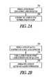
- FIG. 2Ashows a flow diagram of features of an embodiment for forming a hafnium tantalum oxynitride film using atomic layer deposition and nitridization.
- FIG. 2Bshows a flow diagram of features of an embodiment for forming hafnium tantalum oxide using atomic layer deposition for nitridization to a hafnium tantalum oxynitride film.
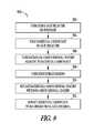
- FIG. 3shows a flow diagram of features of an embodiment for forming a hafnium tantalum oxynitride film using atomic layer deposition and oxidation.
- FIG. 4shows a flow diagram of features of an embodiment for forming hafnium tantalum oxynitride film using atomic layer deposition and annealing.
- FIGS. 5A-5Eillustrate an embodiment of a process for forming a metal substituted electrode.
- FIG. 6illustrates a flow diagram of features of an embodiment of a metal substitution technique.
- FIGS. 7A-7Dillustrate an embodiment of a process for forming a self-aligned conductive layer.
- FIG. 8illustrates an embodiment of a method for forming a self aligned metal gate on high- ⁇ gate dielectrics containing a hafnium tantalum oxynitride film.
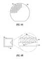
- FIG. 9A-Billustrate a wafer containing integrated circuits having a hafnium tantalum oxynitride film.
- FIG. 10shows an embodiment of a transistor having a dielectric layer including a hafnium tantalum oxynitride film.
- FIG. 11shows an embodiment of a floating gate transistor having a dielectric layer including a hafnium tantalum oxynitride film.
- FIG. 12shows an embodiment of a capacitor having a dielectric layer including a hafnium tantalum oxynitride film.
- FIG. 13depicts an embodiment of a dielectric layer having multiple layers including a hafnium tantalum oxynitride layer.
- FIG. 14is a simplified diagram for an embodiment of a controller coupled to an electronic device having a dielectric layer including a hafnium tantalum oxynitride film.
- FIG. 15illustrates a diagram for an embodiment of an electronic system including devices with a dielectric film including a hafnium tantalum oxynitride film.
- the dielectric regionmay have a reduced equivalent oxide thickness (t eq ).
- the equivalent oxide thicknessquantifies the electrical properties, such as capacitance, of a dielectric in terms of a representative physical thickness.
- T eqis defined as the thickness of a theoretical SiO 2 layer that would be required to have the same capacitance density as a given dielectric, ignoring leakage current and reliability considerations.
- a SiO 2 layer of thickness t, deposited on a silicon surfacemay have a t eq larger than its thickness t.
- This t eqresults from the capacitance in the surface on which the SiO 2 is deposited due to the formation of a depletion/inversion region.
- This depletion/inversion regioncan result in t eq being from 3 to 6 Angstroms ( ⁇ ) larger than the SiO 2 thickness, t.
- the physical thickness requirement for a SiO 2 layer used for a gate dielectricmay be approximately 4 to 7 ⁇ . Additional requirements on a SiO 2 layer would depend on the electrode used in conjunction with the SiO 2 dielectric.
- SiO 2is used as a dielectric layer in devices, in part, due to its electrical isolation properties in a SiO 2 —Si based structure. This electrical isolation is due to the relatively large band gap of SiO 2 (8.9 eV), making it a good insulator from electrical conduction. Significant reductions in its band gap may eliminate it as a material for a dielectric region in an electronic device. As the thickness of a SiO 2 layer decreases, the number of atomic layers or monolayers of the material decreases. At a certain thickness, the number of monolayers will be sufficiently small that the SiO 2 layer will not have a complete arrangement of atoms as in a larger or bulk layer.
- a thin SiO 2 layer of only one or two monolayersmay not form a full band gap.
- the lack of a full band gap in a SiO 2 dielectricmay cause an effective short between an underlying electrode and an overlying electrode.
- This undesirable propertysets a limit on the physical thickness to which a SiO 2 layer can be scaled.
- the minimum thickness due to this monolayer effectis thought to be about 7-8 ⁇ . Therefore, for future devices to have a t eq less than about 10 ⁇ , other dielectrics than SiO 2 may be considered for use as a dielectric region in such future devices.
- materials with a dielectric constant greater than that of SiO 2 , 3.9will have a physical thickness that can be considerably larger than a desired t eq , while providing the desired equivalent oxide thickness.
- an alternative dielectric material with a dielectric constant of 10could have a thickness of about 25.6 ⁇ to provide a t eq of 10 ⁇ , not including any depletion/inversion layer effects.
- a reduced equivalent oxide thickness for transistorscan be realized by using dielectric materials with higher dielectric constants than SiO 2 .
- silicon-based devicesmay employ a dielectric material grown on a silicon substrate or a silicon layer, which places significant constraints on the substitute dielectric material.
- a dielectric materialgrown on a silicon substrate or a silicon layer, which places significant constraints on the substitute dielectric material.
- a small layer of SiO 2could be formed in addition to the desired dielectric.
- the resultwould effectively be a dielectric layer consisting of two sublayers in parallel with each other and the silicon layer on which the dielectric is formed. In such a case, the resulting capacitance would be that of two dielectrics in series.
- t eqt SiO2 +( ⁇ ox / ⁇ ) t.
- SiO 2as a dielectric layer in a device
- the formation of the SiO 2 layerresults in an amorphous dielectric.
- Having an amorphous structure for a dielectrictends to reduce leakage current associated with grain boundaries in polycrystalline dielectrics that provide high leakage paths.
- grain size and orientation changes throughout a polycrystalline dielectriccan cause variations in the film's dielectric constant, along with uniformity and surface topography problems.
- Materials having a high dielectric constant relative to SiO 2may also have a crystalline form, at least in a bulk configuration.
- Good candidates for replacing SiO 2 as a dielectric in a deviceare those that can be fabricated as a thin layer with an amorphous form and that have high dielectric constants.
- Capacitor applicationshave used high- ⁇ dielectric materials, which are insulating materials having a dielectric constant greater than silicon dioxide.
- Such high- ⁇ dielectric materialsinclude silicon oxynitride (SiON, ⁇ ⁇ 6), alumina (Al 2 O 3 , ⁇ ⁇ 9), and oxide/nitride composites (SiO 2 /Si 3 N 4 , ⁇ ⁇ 6).
- Other possible candidatesinclude metal oxides ( ⁇ ⁇ 8-80), nitrides ( ⁇ ⁇ 7-30), oxynitrides ( ⁇ ⁇ 6-25), silicates ( ⁇ ⁇ 6-20), carbides ( ⁇ ⁇ 6-15), and complex titanates ( ⁇ ⁇ >100).
- Factors for selecting appropriate materialsinclude physical, chemical and thermal stability as well as etch-ability and stoichiometric reproducibility. In field effect transistor (FET) applications, there are other factors to consider while addressing device scalability.
- the selected dielectricshould provide stable amorphous and adherent films in the thickness range of 1 nm to 100 nm at temperatures ranging from room temperature to 1000° C.
- a relatively defect-free compositionthat is uniform and reproducible with a fixed charge density and trap density of less than 10 11 cm ⁇ 2 in films of such composition is a factor.
- Another factorincludes dielectric materials that provide a stable non-reactive interface with a silicon substrate such that the interface has an interface state density much less than 10 11 cm ⁇ 2 .
- Such interface state densitiesmay occur when silicon bonds at the interface are saturated with high strength covalent bonds with molecular elements of the dielectric material.
- Yet another factordeals with current transport through the dielectric that should be controlled by tunneling, which is independent of temperature, rather than by trap-assisted thermally dependent transport.
- the conductivity of the dielectricshould be equal to or lower than SiO 2 films when voltage is stressed to a field strength of 5 ⁇ 10 6 V/cm.
- a dielectric material having a bandgap greater than 5 eV and having an electron and hole barrier height greater than 2 eV at a silicon interfacemay be considered.
- An additional factor to consideris using dielectric materials with a destructive breakdown strength greater than 6 ⁇ 10 6 V/cm.
- processing characteristicsinclude compatibility with gate material, selective etch-ability, chemical inertness to contaminants, dopant and post processing environments (temperature, pressure, ambients), and intrinsic properties associated with annealing of defects/damages caused by post-processing such as ion-implantation, plasma-radiation, and gate/back-end processing.
- mixed metal oxynitridesare constructed as dielectric films in a variety of electronic devices and systems. Most oxynitrides are thermally stable and can integrate into semiconductor device processing. With nitrogen concentration in an oxynitride film at 30% or higher, such oxynitrides are considered chemically inert. With processing conditions controlled to provide very low partial pressures of hydrogen and ON ions, oxynitride films with a wide range of nitrogen to oxygen ratio can be deposited over a silicon substrate with very low fixed charge and interface states density. On the other hand, charge trapping and transport characteristics are dependent on the relative ratio of nitrogen to oxygen content in the constructed film.
- Films with nitrogen concentration twice that of oxygenhave a lower bandgap, higher trap density, and transport characteristics dominated by Frenkel-Poole conduction. Such materials may not be well-suited for gate dielectric applications. However, such films also exhibit higher ⁇ values. With increasing oxygen concentration in oxynitride films, the bandgap is raised, current leakage is reduced, and the low frequency ⁇ value is also somewhat reduced. In addition with increasing oxygen concentration, the trap density is reduced, the trap energy depth is increased, and the carrier transport ceases to be trap-assisted, exhibits tunneling conduction, with a weakened temperature dependence.
- a dielectric layerincludes an oxynitride film having approximately 30 atomic % oxygen and approximately 30-35 atomic % nitrogen. With high enough nitrogen content, oxygen-vacancy induced defects in films may be negligible when compared with metal oxides.
- Silicon oxynitridemay be used as a gate dielectric and gate insulator for a non-volatile FET device.
- Aluminum oxynitride (AlON)is expected to have a bandgap greater than 5 eV with a ⁇ value similar to SiON.
- metal oxynitridessuch as ZrON, HfON, LaON, and TaON and other single metal oxynitrides are expected to have a lower bandgap.
- bimetal (or metal/silicon) oxynitridesbased on Si, Al, Hf, La, and Ta are used as dielectric films in a variety of electronic devices and systems. These bimetal oxynitrides may provide a bandgap range from 5 eV to greater than 7 eV.
- bandgapsinclude a bandgap of Si—Al—ON of greater than 7 eV, a bandgap of Si—Hf—ON of about 6.9 eV, a bandgap of Al—Hf—ON of about 6.8 eV, a bandgap of Si—Ta—ON of about 6 eV, a bandgap of Al—Ta—ON of about 6 eV.
- Bimetal oxynitrides Hf—Ta—ON, Hf—La—ON, Al—La—ON, Ta—La—ON, and Si—La—ONare estimated to exhibit significantly lower bandgaps.
- the ⁇ value for Si—Al—ONis estimated at approximately 7 to 8, while the ⁇ values for the other oxynitrides of this group are estimated to be in the range from about 15 to 25.
- Refractory metalssuch as tungsten, molybdenum, tantalum, niobium, chromium, vanadium, and rhenium are metals with a melting point significantly higher than non-refractory metals.
- Transition metalsare typically considered any element with an incomplete d subshell and include generally those elements between the group 2 elements and group 13 elements of the periodic table. Examples of transition metals include hafnium, yttrium, zirconium, platinum as well as the refractory metals.
- a refractory metal and a non-refractory metalare used to form a dielectric.
- a refractory metal and a non-refractory metalare used in combination with oxygen and nitrogen to form a dielectric.
- combinations of a refractory oxide, a refractory nitride and a refractory oxynitrideform a dielectric.
- the refractory-based dielectricis amorphous. In some embodiments, the refractory-based dielectric is homogenous.
- a refractory metal and a non-refractory transition metalform a dielectric.
- Various embodimentsmay include using a refractory metal and a non-refractory transition metal to form a plurality of layers.
- stacked dielectric layersare formed using a refractory metal and a non-refractory transition metal in combination with oxygen and/or nitrogen.
- Various embodimentsinclude forming a stacked dielectric structure using refractory metal oxides, refractory metal nitrides, refractory metal oxynitrides in combination with non-refractory metal oxides, non-refractory metal nitrides, and non-refractory metal oxynitrides.
- forming a stacked dielectric structure using refractory metal oxides, refractory metal nitrides, refractory metal oxynitrides in combination with non-refractory transition metal oxides, non-refractory transition metal nitrides, and non-refractory transition metal oxynitridesare formed using refractory metal oxides, refractory metal nitrides, refractory metal oxynitrides in combination with non-refractory transition metal oxides, non-refractory transition metal nitrides, and non-refractory transition metal oxynitrides.
- one or more of the refractory metal, non-refractory metal, oxygen and nitrogen concentrationis graded substantially perpendicular to direction of deposition or to a surface normal.
- one or more of the refractory metal, non-refractory metal, oxygen and nitrogen concentrationis graded substantially parallel to direction of deposition or substantially parallel to the surface of the substrate.
- a film of hafnium tantalum oxynitrideis used as a dielectric layer for application in a variety of electronic devices, replacing the use of silicon oxide to provide a higher dielectric constant.
- a high-k gate dielectricincludes one or more of the following: TaN, HfN, HfON, TaON, HfTaON, TaN/HfN, TaN/HfON, TaON/HfN, TaON/HfON, TaN/HfO 2 , Ta 2 O 5 /HfN, TaON/HfO 2 , Ta 2 O 5 /HfON, and Ta 2 O 5 /HfO 2 .
- a dielectric layeris constructed containing hafnium tantalum oxynitride formed using atomic layer deposition with a metal electrode formed in contact with the dielectric layer.
- the metal electrodemay also be formed by atomic layer deposition.
- the metal electrodemay be formed by substituting a desired metal material for a previously disposed substitutable material.
- the metal electrodemay be formed as a self aligned metal electrode on and contacting the dielectric layer.
- the metal electrodemay be formed on the dielectric layer using a previously disposed sacrificial carbon layer on the dielectric layer and sacrificial carbon sidewall spacers adjacent to the sacrificial carbon layer.
- hafnium tantalum oxynitrideis used herein with respect to a composition that essentially consists of hafnium, tantalum, oxygen, and nitrogen in a form that may be stoichiometric, non-stoichiometric, or a combination of stoichiometric and non-stoichiometric.
- a hafnium tantalum oxynitride filmmay also be referred to as a hafnium tantalum oxygen nitrogen film.
- Other nomenclature for a composition that essentially consists of hafnium, tantalum, oxygen, and nitrogenmay be known to those skilled in the art.
- hafnium tantalum oxynitridemay be formed substantially as a stoichiometric hafnium tantalum oxynitride film. In an embodiment, hafnium tantalum oxynitride may be formed substantially as a non-stoichiometric hafnium tantalum oxynitride film. In an embodiment, hafnium tantalum oxynitride may be formed substantially as a combination film of non-stoichiometric hafnium tantalum oxynitride and stoichiometric hafnium tantalum oxynitride.
- a hafnium tantalum oxynitride compositionmay be expressed as HfTaON, Hf x Ta y O z N w , or other equivalent form.
- HfTaON or its equivalent formsmay be used to include HfTaON in a form that is stoichiometric, non-stoichiometric, or a combination of stoichiometric and non-stoichiometric hafnium tantalum oxynitride.
- the expression HfTaON or its equivalent formsmay be used to include HfTaON in a form that is homogeneous and amorphous hafnium tantalum oxynitride.
- TaO, Ta y O z , or its equivalent formsmay be used to include tantalum oxide in a form that is stoichiometric, non-stoichiometric, or a combination of stoichiometric and non-stoichiometric.
- expressionssuch as TaO, TaN, TaON, Ta y O z , HfO z , HfN w , HfON, Hf x O z N w , etc. may be used.
- x, y, w, and zare atomic mole fractions. In various embodiments, x, y, w, and z are atomic percentages. In some embodiments, x, y, w and z represent a particular chemical composition as is known in the art.
- Forms that are stoichiometric, non-stoichiometric, or a combination of stoichiometric and non-stoichiometricmay include expressions such as TaN, HfN, HfON, TaON, HfTaON, TaN/HfN, TaN/HfON, TaON/HfN, TaON/HfON, TaN/HfO 2 , Ta 2 O 5 /HfN, TaON/HfO 2 , Ta 2 O 5 /HfON, and Ta 2 O 5 /HfO 2 .
- a hafnium tantalum oxynitride filmis doped with elements or compounds other than hafnium, tantalum, oxygen, and nitrogen.
- a hafnium tantalum oxynitride dielectric filmmay be formed using atomic layer deposition (ALD). Forming such structures using atomic layer deposition may allow control of transitions between material layers. As a result of such control, atomic layer deposited hafnium tantalum oxynitride dielectric films can have an engineered transition with a surface on which it is formed.
- ALDatomic layer deposition
- ALDalso known as atomic layer epitaxy (ALE)
- ALEatomic layer epitaxy
- CVDchemical vapor deposition
- ALDalternatively pulsed-CVD
- gaseous precursorsare introduced one at a time to the substrate surface mounted within a reaction chamber (or reactor). This introduction of the gaseous precursors takes the form of pulses of each gaseous precursor.
- the precursor gasis made to flow into a specific area or region for a short period of time.
- the reaction chambermay be purged with a gas, where the purging gas may be an inert gas.
- the reaction chambermay be evacuated.
- the reaction chambermay be purged with a gas and evacuated.
- CS-ALDchemisorption-saturated ALD
- the second pulsing phaseintroduces another precursor on the substrate where the growth reaction of the desired film takes place. Subsequent to the film growth reaction, reaction byproducts and precursor excess are purged from the reaction chamber. With favorable precursor chemistry where the precursors absorb and react with each other aggressively on the substrate, one ALD cycle can be performed in less than one second in properly designed flow type reaction chambers.
- precursor pulse timesrange from about 0.5 sec to about 2 to 3 seconds. Pulse times for purging gases may be significantly longer, for example, pulse times of about 5 to about 30 seconds.
- ALDALD
- the saturation of all the reaction and purging phasesmakes the growth self-limiting.
- This self-limiting growthresults in large area uniformity and conformality, which has important applications for such cases as planar substrates, deep trenches, and in the processing of porous silicon and high surface area silica and alumina powders.
- Atomic layer depositionprovides control of film thickness in a straightforward manner by controlling the number of growth cycles.
- the precursors used in an ALD processmay be gaseous, liquid or solid. However, liquid or solid precursors should be volatile. The vapor pressure should be high enough for effective mass transportation. Also, solid and some liquid precursors may be heated inside the atomic layer deposition system and introduced through heated tubes to the substrates. The necessary vapor pressure should be reached at a temperature below the substrate temperature to avoid the condensation of the precursors on the substrate. Due to the self-limiting growth mechanisms of ALD, relatively low vapor pressure solid precursors can be used, though evaporation rates may vary somewhat during the process because of changes in their surface area.
- precursors used in ALDthere are several other characteristics for precursors used in ALD.
- the precursorsshould be thermally stable at the substrate temperature, because their decomposition may destroy the surface control and accordingly the advantages of the ALD method that relies on the reaction of the precursor at the substrate surface. A slight decomposition, if slow compared to the ALD growth, may be tolerated.
- the precursorsshould chemisorb on or react with the surface, though the interaction between the precursor and the surface as well as the mechanism for the adsorption is different for different precursors.
- the molecules at the substrate surfaceshould react aggressively with the second precursor to form the desired solid film. Additionally, precursors should not react with the film to cause etching, and precursors should not dissolve in the film. Using highly reactive precursors in ALD contrasts with the selection of precursors for conventional CVD.
- the by-products in the reactionshould be gaseous in order to allow their easy removal from the reaction chamber. Further, the by-products should not react or adsorb on the surface.
- RS-ALDreaction sequence ALD
- the self-limiting process sequenceinvolves sequential surface chemical reactions.
- RS-ALDrelies on chemistry between a reactive surface and a reactive molecular precursor.
- molecular precursorsare pulsed into the ALD reaction chamber separately.
- a metal precursor reaction at the substratemay be followed by an inert gas pulse to remove excess precursor and by-products from the reaction chamber prior to pulsing the next precursor of the fabrication sequence.
- filmscan be layered in equal metered sequences that may all be substantially identical in chemical kinetics, deposition per cycle, composition, and thickness.
- RS-ALD sequencesgenerally deposit less than a full layer per cycle. Typically, a deposition or growth rate of about 0.25 to about 2.00 ⁇ per RS-ALD cycle may be realized.
- a sequencerefers to ALD material formation based on an ALD reaction of a precursor with its reactant precursor.
- forming hafnium nitride from a HfCl 4 precursor and NH 3 , as its reactant precursorincludes a hafnium/nitrogen sequence.
- a reactant precursor that contains nitrogenis used to supply nitrogen.
- a precursor that contains nitrogen and that supplies nitrogen to be incorporated in the ALD composition formedwhich may be used in an ALD process with precursors supplying the other elements in the ALD composition, is referred to as a nitrogen reactant precursor.
- NH 3is a nitrogen reactant precursor.
- an ALD sequence for a metal oxidemay be referenced with respect to the metal and oxygen.
- an ALD sequence for hafnium oxidemay also be referred to as a hafnium/oxygen sequence.
- a reactant precursor that contains oxygenis used to supply the oxygen.
- a precursor that contains oxygen and that supplies oxygen to be incorporated in the ALD composition formedwhich may be used in an ALD process with precursors supplying the other elements in the ALD composition, is referred to as an oxygen reactant precursor.
- water vaporis an oxygen reactant precursor.
- An ALD cyclemay include pulsing a precursor, pulsing a purging gas for the precursor, pulsing a reactant precursor, and pulsing the reactant precursor's purging gas.
- An ALD cyclemay include pulsing a precursor, evacuating the reactant chamber, pulsing a reactant precursor, and evacuating the reactant chamber.
- An ALD cyclemay include pulsing a precursor, pulsing a purging gas for the precursor and evacuating the reactant chamber, pulsing a reactant precursor, and pulsing the reactant precursor's purging gas and evacuating the reactant chamber.
- tantalum oxidefrom a TaCl 5 precursor and H 2 O, as its reactant precursor, forms an embodiment of a tantalum/oxygen sequence, which can also be referred to as a tantalum sequence. Additional information regarding tantalum oxides formed by ALD can be found in U.S. patent application Ser. No. 11/029,757, referenced previously.
- an ALD sequencemay deal with pulsing a reactant precursor to the substrate surface on which a metal-containing species has been absorbed such that the reactant precursor reacts with the metal-containing species resulting in the deposited metal and a gaseous by-product that can be removed during the subsequent purging/evacuating process.
- an ALD sequencemay include reacting a precursor containing the metal species with a substrate surface.
- a cycle for such a metal forming sequencemay include pulsing a purging gas after pulsing the precursor containing the metal species to deposit the metal.
- deposition of a semiconductor materialmay be realized in a manner similar to forming a layer of a metal, given the appropriate precursors for the semiconductor material.
- a cyclemay include a number of sequences to provide the elements of the composition.
- a cycle for an ALD formation of an ABO x compositionwhere “A” is a first element, e.g., a metal, and “B” is a second element, e.g., a metal, may include sequentially [pulsing a first precursor/a purging gas for the first precursor/a first reactant precursor/the first reactant precursor's purging gas] followed sequentially by [a second precursor/a purging gas for the second precursor/a second reactant precursor/the second reactant precursor's purging gas], which may be viewed as a cycle having two sequences.
- a cyclemay include a number of sequences for element A and a different number of sequences for element B.
- ALD formation of an ABO x compositionuses one precursor that contains the elements A and B, such that pulsing the AB containing precursor followed by its reactant precursor onto a substrate may include a reaction that forms ABO x on the substrate to provide an AB/oxygen sequence.
- a cycle of an AB/oxygen sequencemay include pulsing a precursor containing A and B, pulsing a purging gas for the precursor, pulsing an oxygen reactant precursor to the A/B precursor, and pulsing a purging gas for the reactant precursor.
- a cyclemay be repeated a number of times to provide a desired thickness of the composition.
- a cycle for an ALD formation of the quaternary composition, hafnium tantalum oxygen nitrogenmay include sequentially [pulsing a first precursor/a purging gas for the first precursor/a first reactant precursor/the first reactant precursor's purging gas] followed sequentially by [a second precursor/a purging gas for the second precursor/a second reactant precursor/the second reactant precursor's purging gas/a third precursor/a purging gas for the third precursor/a third reactant precursor/the third reactant precursor's purging gas], which may be viewed as a cycle having three sequences.
- a layer substantially of a hafnium tantalum oxynitride compositionis formed on a substrate mounted in a reaction chamber using ALD in repetitive tantalum/oxygen and hafnium/nitrogen sequences using precursor gases individually pulsed into the reaction chamber.
- a layer substantially of a hafnium tantalum oxynitride compositionis formed on a substrate mounted in a reaction chamber using ALD in repetitive tantalum/nitrogen and hafnium/oxygen sequences using precursor gases individually pulsed into the reaction chamber.
- a substantially hafnium tantalum oxynitride compositionis formed by ALD having approximately 30% nitrogen and 30% oxygen concentrations in the resultant HfTaON dielectric film.
- a substantially pure hafnium tantalum oxynitride compositionis formed by ALD having approximately 20-40% nitrogen and 20-40% oxygen concentrations in the resultant HfTaON dielectric film.
- FIG. 1depicts an embodiment of an atomic layer deposition system 100 for processing a hafnium tantalum oxynitride according to various embodiments of the invention.
- the elements depictedare used to discuss various embodiments for forming HfTaON such that those skilled in the art may practice the present invention without undue experimentation.
- a substrate 110is located inside a reaction chamber 120 of ALD system 100 .
- reaction chamber 120may be located a heating element 130 , which is thermally coupled to substrate 110 to control the substrate temperature.
- a gas-distribution fixture 140introduces precursor gases to the substrate 110 . Each precursor gas originates from individual gas sources 150 - 155 whose flow is controlled by gas controllers 156 - 161 , respectively.
- gas controllersinclude flow switches such as mass-flow controllers, ultrasound meters, and rotameters.
- Gas sources 150 - 155provide a precursor gas either by storing the precursor as a gas or by providing a location and apparatus for evaporating a solid or liquid material to form the selected precursor gas. Furthermore, additional gas sources may be included, one or more for each metal precursor employed and one or more for each reactant precursor associated with each metal precursor, if desired.
- purging gas sources 163 , 164may be also included in the ALD system.
- additional purging gas sourcesmay be constructed in ALD system 100 , one purging gas source for each precursor gas. For a process that uses the same purging gas for multiple precursor gases, less purging gas sources are required for ALD system 100 .
- Gas sources 150 - 155 and purging gas sources 163 - 164are coupled by their associated gas controllers to a common gas line or conduit 170 , which is coupled to the gas-distribution fixture 140 inside reaction chamber 120 .
- Gas conduit 170is also coupled to vacuum pump, or exhaust pump, 181 by gas controller 186 to remove excess precursor gases, purging gases, and by-product gases at the end of a purging sequence from gas conduit 170 .
- the vacuum pump, or exhaust pump, 182may be coupled to chamber 120 using gas controller 187 to remove excess precursor gases, purging gases, and by-product gases at the end of a purging sequence from reaction chamber 120 .
- gas controller 187to remove excess precursor gases, purging gases, and by-product gases at the end of a purging sequence from reaction chamber 120 .
- control displays, mounting apparatus, temperature sensing devices, substrate maneuvering apparatus, and necessary electrical connections known to those skilled in the artare not shown in FIG. 1 .
- the use, construction and fundamental operation of reaction chambers for deposition of filmsare understood by those of ordinary skill in the art of semiconductor fabrication. Embodiments of the present invention may be practiced on a variety of such reaction chambers without undue experimentation.
- one of ordinary skill in the artwill comprehend the necessary detection, measurement, and control techniques in the art of semiconductor fabrication upon reading this disclosure.
- a hafnium tantalum oxynitride layeris structured as one or more monolayers with a thickness ranging from a monolayer to thousands of angstroms or more.
- the filmmay be processed using atomic layer deposition.
- Embodiments of an atomic layer deposited hafnium tantalum oxynitride layerhave a larger dielectric constant than silicon dioxide.
- Such dielectric layersprovide a significantly thinner equivalent oxide thickness compared with a silicon oxide layer having the same physical thickness.
- such dielectric layersprovide a significantly thicker physical thickness than a silicon oxide layer having the same equivalent oxide thickness. This increased physical thickness aids in reducing leakage current.
- the surface on which the hafnium tantalum oxynitride film is to be depositedmay undergo a preparation stage.
- the surfacemay be the surface of a substrate for an integrated circuit.
- the substrate used for forming a transistormay include a silicon or silicon containing material.
- silicon germanium, germanium, gallium arsenide, silicon-on-sapphire substrates, or other suitable substratesmay be used.
- a preparation processmay include cleaning the substrate and forming layers and regions of the substrate, such as drains and sources, prior to forming a gate dielectric in the formation of a metal oxide semiconductor (MOS) transistor.
- MOSmetal oxide semiconductor
- active regionsmay be formed after forming the dielectric layer, depending on the over-all fabrication process implemented.
- the substrateis cleaned to provide an initial substrate depleted of its native oxide.
- the initial substrateis cleaned also to provide a hydrogen-terminated surface.
- a silicon substrateundergoes a final hydrofluoric (HF) rinse prior to ALD processing to provide the silicon substrate with a hydrogen-terminated surface without a native silicon oxide layer.
- HFfinal hydrofluoric
- Cleaning immediately preceding atomic layer depositionaids in reducing an occurrence of silicon oxide as an interface between a silicon-based substrate and a hafnium tantalum oxynitride dielectric formed using the atomic layer deposition process.
- the material composition of an interface layer and its propertiesare typically dependent on process conditions and the condition of the substrate before forming the dielectric layer. Though the existence of an interface layer may effectively reduce the dielectric constant associated with the dielectric layer and its substrate interface layer, a SiO 2 interface layer or other composition interface layer may improve the interface density, fixed charge density, and channel mobility of a device having this interface layer.
- the sequencing of the formation of the regions of an electronic devicemay follow sequencing that is generally performed in the fabrication of such devices as is well known to those skilled in the art. Included in the processing prior to forming a dielectric may be the masking of substrate regions to be protected during the dielectric formation, as is typically performed in semiconductor fabrication. In an embodiment, an unmasked region includes a body region of a transistor; however, one skilled in the art will recognize that other semiconductor device structures may utilize this process.
- a purging gasis pulsed into the ALD reaction chamber.
- the ALD reactor chambermay be evacuated using vacuum techniques as is known by those skilled in the art.
- a purging gasmay be pulsed into the ALD reaction chamber and the ALD reactor chamber may be evacuated.
- an ALD cycle for forming HfTaONincludes sequencing component-containing precursors in the order of tantalum, oxygen, hafnium, and nitrogen with appropriate purging between the different component-containing precursors. Full coverage or partial coverage of a monolayer on a substrate surface may be attained for pulsing of a metal-containing precursor.
- an ALD cycle for forming HfTaONincludes sequencing the component-containing precursors in various permutations.
- an ALD cycle to form hafnium tantalum oxynitrideincludes a number, x, of tantalum/oxygen sequences and a number, y, of hafnium/nitrogen sequences.
- an ALD cycle to form hafnium tantalum oxynitrideincludes a number, x, of tantalum/nitrogen sequences and a number, y, of hafnium/oxygen sequences.
- the number of sequences x and yis determined by selecting the relative amounts of hafnium, tantalum, oxygen, and nitrogen.
- the number of sequences x and ymay be selected to form hafnium tantalum oxynitride that is a nitrogen-rich relative to the amount of oxygen in the dielectric.
- the number of sequences x and ymay be selected to form hafnium tantalum oxynitride that is oxygen-rich relative to the amount of nitrogen in the dielectric.
- the hafnium tantalum oxynitridemay be formed as a tantalum-rich dielectric relative to the amount of hafnium in the dielectric.
- the hafnium tantalum oxynitridemay be formed as a hafnium-rich dielectric relative to the amount of tantalum in the dielectric.
- the pulsing of the individual component-containing precursorsmay be performed independently in a non-overlapping manner using the individual gas sources 150 - 155 and flow controllers 156 - 161 of ALD system 100 of FIG. 1 .
- Each precursormay be pulsed into the reaction chamber 120 for a predetermined period, where the predetermined period can be set separately for each precursor. Additionally, for various ALD formations, each precursor may be pulsed into the reaction chamber under separate environmental conditions.
- the substratemay be maintained at a selected temperature and the reaction chamber 120 maintained at a selected pressure independently for pulsing each precursor. Appropriate temperatures and pressures may be maintained, whether the precursor is a single precursor or a mixture of precursors.
- a number of precursors containing tantalummay be used to provide the tantalum to a substrate for an integrated circuit.
- a precursor containing a tantalumincludes, but is not limited to TaCl 5 , (Ta(N-t-C 5 H 11 )[N(CH 3 ) 2 ] 3 , and tantalum ethoxide Ta(OC 2 H 5 ) 5 .
- H 2is pulsed along with a precursor to reduce carbon contamination in the fabricated film.
- a tantalum-containing precursoris pulsed onto a substrate in an ALD reaction chamber.
- a reactant precursoris pulsed into the reaction chamber.
- the reactant precursormay be an oxygen reactant precursor that may include, but is not limited to, one or more of water, atomic oxygen, molecular oxygen, ozone, hydrogen peroxide, a water-hydrogen peroxide mixture, alcohol, or nitrous oxide.
- the pulsing of the tantalum precursormay use a pulsing period that provides uniform coverage of a monolayer on the surface or may use a pulsing period that provides partial coverage of a monolayer on the surface during a tantalum sequence.
- a number of precursors containing hafniummay be used to provide the hafnium to a substrate for an integrated circuit.
- a precursor containing hafniummay include anhydrous hafnium nitride, Hf(NO 3 ) 4 .
- the substrate temperatureis maintained at a temperature ranging from about 160° C. to about 180° C.
- a hafnium precursorincludes HfCl 4 .
- the substrate temperatureis maintained at a temperature ranging from about 180° C. to about 600° C.
- the substrate temperatureis maintained at a temperature ranging from about 300° C. to about 940° C.
- a hafnium precursoris HfI 4 .
- the substrate temperatureis maintained at a temperature of about 300° C.
- Hafnium oxidemay be grown by ALD using a Hf[N(CH 3 )(C 2 H 5 )] 4 , which may be known as a homoleptic tetrakis(dialkylamino) hafnium(IV) compound, and water as an oxygen reactant.
- hafnium tetrakis(dialkylamino) hafnium compoundsmay also be used, such as hafnium tetrakis dimethylamine, Hf[N(CH 3 ) 2 ] 4 , or hafnium tetrakis diethylamine, Hf[N(C 2 H 5 ) 2 ] 4 , as a hafnium-containing precursor.
- hafnium tetrakis dimethylamineHf[N(CH 3 ) 2 ] 4
- hafnium tetrakis diethylamineHf[N(C 2 H 5 ) 2 ] 4
- use of the individual hafnium-containing precursorsis not limited to the temperature ranges of the above example embodiments.
- the pulsing of the hafnium precursormay use a pulsing period that provides uniform coverage of a monolayer on the surface or may use a pulsing period that provides partial coverage of a monolayer on the surface during a hafnium sequence.
- nitrogenis used as a purging gas and a carrier gas for one or more of the sequences used in the ALD formation of hafnium tantalum oxynitride.
- hydrogen, argon gas, or other inert gasesmay be used as the purging gas.
- Excess precursor gas and reaction by-productsmay be removed by the purge gas.
- Excess precursor gas and reaction by-productsmay be removed by evacuation of the reaction chamber using various vacuum techniques.
- Excess precursor gas and reaction by-productsmay be removed by the purge gas and by evacuation of the reaction chamber.
- the thickness of a hafnium tantalum oxynitride layer formed by atomic layer depositionis determined by a fixed growth rate for the pulsing periods and precursors used, set at a value such as N nm/cycle, and the number of cycles conducted.
- the processis conducted in an ALD window, which is a range of temperatures in which the growth rate is substantially constant. In an embodiment, if such an ALD window is not available, the ALD process is conducted at the same set of temperatures for each ALD sequence in the process. For a desired hafnium tantalum oxynitride layer thickness, t, in an application, the ALD process is repeated for t/N total cycles. Once the t/N cycles have completed, further ALD processing for the hafnium tantalum oxynitride layer may be terminated. In an embodiment, a hafnium tantalum oxynitride layer processed at relatively low temperatures associated with atomic layer deposition provides an amorphous layer.
- a HfTaON filmis grown to a desired thickness by repetition of a process including atomic layer deposition of layers of Ta 2 O 5 and HfN and/or layers of HfO 2 and TaN followed by annealing.
- a base thicknessis formed according to various embodiments such that forming a predetermined thickness of a HfTaON film may be conducted by forming a number of layers having the base thickness. As can be understood by one skilled in the art, determining the base thickness depends on the application and can be determined during initial processing without undue experimentation.
- Relative amounts of hafnium, tantalum, oxygen, and nitrogen in a HfTaON filmmay be controlled by regulating the relative thicknesses of the individual layers of oxides and nitrides formed.
- relative amounts of hafnium, tantalum, oxygen, and nitrogen in a HfTaON filmmay be controlled by forming a layer of HfTaON as multiple layers of different base thickness and by regulating the relative thicknesses of the individual layers of oxides and nitrides formed in each base layer prior to annealing.
- particular effective growth rates for the selected hafnium tantalum oxynitride filmcan be determined during normal initial testing of the ALD system used in processing a hafnium tantalum oxynitride dielectric for a given application without undue experimentation.
- FIG. 2Ashows a flow diagram of features of an embodiment for forming HfTaON using atomic layer deposition and nitridization.
- a layer of HfTaOis formed using atomic layer deposition.
- the layer of HfTaOis subjected to nitridization to form a HfTaON film.
- the nitridizationmay be a high temperature nitridization.
- active nitrogenmay be introduced by microwave plasma.
- active nitrogenmay be introduced by a NH 3 anneal.
- a high temperature nitridizationis a nitridizing process that is performed at temperatures equal to or above 500° C.
- HfTaOis formed by atomic layer deposition using ALD cycles of tantalum/oxygen sequences and hafnium/oxygen sequences.
- ALD cyclecan be selected from a number of different permutations of tantalum/oxygen sequences and hafnium/oxygen sequences.
- FIG. 2Bshows a flow diagram of features of an embodiment for forming HfTaO using atomic layer deposition for nitridization to a HfTaON film.
- a layer of tantalum oxideis formed on a substrate by atomic layer deposition.
- a layer of hafnium oxideis formed by atomic layer deposition on the layer of tantalum oxide.
- the layers of tantalum oxide and hafnium oxideare annealed to form a layer of HfTaO.
- the order of forming Ta 2 O 5 and HfO 2may be interchanged.
- the layer of HfTaOmay be nitridized to form HfTaON.
- the layers of tantalum oxide and hafnium oxidemay be nitridized during the annealing process.
- alternating layers of ALD tantalum oxide and ALD hafnium oxideare formed to a desired thickness prior to nitridization.
- a layer of ALD tantalum oxide and a layer of ALD hafnium oxideare formed, each to a desired thickness, the layers of ALD tantalum oxide and ALD hafnium oxide nitridized to form a HfTaON layer.
- a layer of ALD tantalum oxide and a layer of ALD hafnium oxidemay be formed on the HfTaON layer, the layers of ALD tantalum oxide and ALD hafnium oxide nitridized to form a HfTaON layer on and contiguous with the previously formed HfTaON layer. This process may be continued until the desired thickness of HfTaON is formed.
- ALD Ta 2 O 5is formed using a number of precursors containing tantalum to provide the tantalum to a substrate for an integrated circuit.
- tantalum-containing precursorsinclude, but are not limited to, a tantalum halide precursor, such as TaCl 5 , Ta(N-t-C 5 H 11 )[N(CH 3 ) 2 ] 3 , or tantalum ethoxide Ta(OC 2 H 5 ) 5 .
- an oxygen reactant precursormay be pulsed into the reaction chamber.
- the oxygen reactant precursormay include, but is not limited to, one or more of water, atomic oxygen, molecular oxygen, ozone, hydrogen peroxide, a water-hydrogen peroxide mixture, alcohol, or nitrous oxide.
- the reaction chambermay be purged of excess precursor and by-products.
- the pulsing of the precursorsmay use pulsing periods that provide uniform coverage of a monolayer on the surface or may use pulsing periods that provide partial coverage of a monolayer on the surface during a tantalum/oxygen ALD cycle.
- ALD HfO 2is formed using a number of precursors containing hafnium to provide the hafnium to a substrate for an integrated circuit.
- hafnium-containing precursorsinclude, but are not limited to, a hafnium halide, such as HfCl 4 and HfI 4 , Hf(NO 3 ) 4 , Hf[N(CH 3 )(C 2 H 5 )] 4 , Hf[N(CH 3 ) 2 ] 4 , and Hf[N(C 2 H 5 ) 2 ] 4 .
- an oxygen reactant precursormay be pulsed into the reaction chamber.
- the oxygen reactant precursormay include, but is not limited to, one or more of water, atomic oxygen, molecular oxygen, ozone, hydrogen peroxide, a water-hydrogen peroxide mixture, alcohol, or nitrous oxide.
- the pulsing of the precursorsmay use pulsing periods that provide uniform coverage of a monolayer on the surface or may use pulsing periods that provide partial coverage of a monolayer on the surface during an ALD cycle forming HfO 2 .
- nitrogenis used as a purging gas and a carrier gas for one or more of the sequences.
- hydrogen, argon gas, or other inert gasesmay be used as the purging gas.
- Excess precursor gas and reaction by-productsmay be removed by the purge gas.
- Excess precursor gas and reaction by-productsmay be removed by evacuation of the reaction chamber using various vacuum techniques.
- Excess precursor gas and reaction by-productsmay be removed by the purge gas and by evacuation of the reaction chamber.
- FIG. 3shows a flow diagram of features of an embodiment for forming HfTaON using atomic layer deposition and oxidation.
- a layer of HfNis formed by atomic layer deposition.
- a layer of TaNis formed by atomic layer deposition on the layer of HfN.
- HfN and TaN filmsmay be alternately deposited in adjacent layers, in which either nitride layer may be deposited as the starting layer.
- the layers of TaN and HfNare annealed.
- the annealed layers of TaN and HfNare oxidized to form HfTaON. In an embodiment, the annealing and oxidation may be performed together.
- the layers of TaN and HfNmay be annealed and oxidized by rapid thermal oxidation to form HfTaON.
- ALD HfNis formed using a number of precursors containing hafnium to provide the hafnium to a substrate for an integrated circuit.
- a hafnium-containing precursoris pulsed onto a substrate in an ALD reaction chamber.
- a number of precursors containing hafniummay be used to provide the hafnium to a substrate for an integrated circuit.
- the hafnium-containing precursormay be a hafnium halide precursor, such as HfCl 4 or HfI 4 .
- the hafnium nitridemay be grown by ALD using Hf[N(CH 3 )(C 2 H 5 )] 4 .
- the substrateis held at a temperature ranging from about 150° C. to about 300° C.
- Other types of tetrakis(dialkylamino) metal compoundsmay also be used, such as hafnium tetrakis dimethylamine, Hf[N(CH 3 ) 2 ] 4 , or hafnium tetrakis diethylamine, Hf[N(C 2 H 5 ) 2 ] 4 , as a hafnium-containing precursor.
- a reactant precursoris pulsed into the reaction chamber.
- the reactant precursormay be a nitrogen reactant precursor including, but not limited to, ammonia (NH 3 ).
- Other nitrogen reactant precursors that may be usedinclude nitrogen-containing compositions that do not include oxygen.
- use of the individual hafnium-containing precursorsis not limited to the temperature ranges of the above embodiments.
- forming hafnium nitride by atomic layer depositionis not limited to the abovementioned precursors.
- the pulsing of the hafnium precursormay use a pulsing period that provides uniform coverage of a monolayer on the surface or may use a pulsing period that provides partial coverage of a monolayer on the surface during a hafnium sequence.
- ALD TaNis formed using a number of precursors containing tantalum to provide the tantalum to a substrate for an integrated circuit.
- a tantalum-containing precursoris pulsed onto a substrate in an ALD reaction chamber.
- Precursors containing tantalummay be used to provide the tantalum to a substrate for an integrated circuit.
- the tantalum-containing precursormay be a tantalum halide precursor, such as TaF 5 , TaCl 5 , or Ta(N-t-O 5 H 11 )[N(CH 3 ) 2 ] 3 . Additional information regarding metal nitride layers formed by ALD can be found in U.S.
- H 2is pulsed along with the precursor to reduce carbon contamination in the deposited film.
- a reactant precursormay be pulsed into the reaction chamber.
- a nitrogen reactant precursoris pulsed.
- a number of precursors containing nitrogenmay be used to provide nitrogen.
- nitrogen-containing precursorsinclude, but are not limited to, nitrogen, ammonia (NH 3 ), tert-butylamine (C 4 H 11 N), allylamine (C 3 H 7 N), 1,1-dimethylhydrazine ((CH 3 ) 2 NNH 2 ).
- the substrateis maintained at a temperature ranging from about 400° C. to about 500° C. using tert-butylamine or allylamine as a nitrogen precursor.
- NH 3is pulsed with the tert-butylamine and the allylamine. The addition of NH 3 may enhance the deposition rate at lower temperatures.
- use of the individual tantalum-containing precursorsis not limited to the temperature ranges of the above example embodiments. Further, forming tantalum nitride by atomic layer deposition is not limited to the abovementioned precursors.
- the pulsing of the tantalum precursormay use a pulsing period that provides uniform coverage of a monolayer on the surface or may use a pulsing period that provides partial coverage of a monolayer on the surface during a tantalum/nitrogen sequence.
- nitrogenis used as a purging gas and a carrier gas for one or more of the sequences.
- hydrogen, argon gas, or other inert gasesmay be used as the purging gas.
- Excess precursor gas and reaction by-productsmay be removed by the purge gas.
- Excess precursor gas and reaction by-productsmay be removed by evacuation of the reaction chamber using various vacuum techniques.
- Excess precursor gas and reaction by-productsmay be removed by the purge gas and by evacuation of the reaction chamber.
- FIG. 4shows a flow diagram of features of an embodiment for forming HfTaON using atomic layer deposition and annealing.
- a layer of HfONis formed using atomic layer deposition.
- a layer of TaONis formed using atomic layer deposition on the layer of HfON.
- the layers of HfON and TaONreact during annealing to form a layer of HfTaON.
- HfON and TaON filmsmay be alternately deposited in adjacent layers, in which either oxynitride layer may be deposited as the starting layer.
- ALD TaONis formed using a number of precursors containing tantalum to provide the tantalum to a substrate for an integrated circuit.
- tantalum-containing precursorsinclude, but are not limited to, a tantalum halide, such as TaF 5 , TaCl 5 , or Ta( N-t-C 5 H 11 )[N(CH 3 ) 2 ] 3 , and tantalum ethoxide Ta(OC 2 H 5 ) 5 .
- a reactant precursormay be pulsed into the reaction chamber.
- a nitrogen reactant precursormay be pulsed.
- a number of precursors containing nitrogenmay be used to provide nitrogen.
- nitrogen-containing precursorsinclude, but are not limited to, nitrogen, ammonia (NH 3 ), tert-butylamine (C 4 H 11 N), allylamine (C 3 H 7 N), and 1,1-dimethylhydrazine ((CH 3 ) 2 NNH 2 ).
- an oxygen reactant precursormay be pulsed into the reaction chamber.
- the oxygen reactant precursormay include, but is not limited to, one or more of water, atomic oxygen, molecular oxygen, ozone, hydrogen peroxide, a water-hydrogen peroxide mixture, alcohol, or nitrous oxide.
- the order of pulsing the precursorsmay vary.
- forming tantalum oxynitride by atomic layer depositionis not limited to the abovementioned precursors.
- the pulsing of the precursorsmay use pulsing periods that provide uniform coverage of a monolayer on the surface or may use pulsing periods that provide partial coverage of a monolayer on the surface during an ALD cycle forming TaON.
- ALD HfONis formed using a number of precursors containing hafnium to provide the hafnium to a substrate for an integrated circuit.
- hafnium-containing precursorsinclude, but are not limited to, a hafnium halide, such as HfCl 4 or HfI 4 , Hf[N(CH 3 )(C 2 H 5 )] 4 , hafnium tetrakis dimethylamine, Hf[N(CH 3 ) 2 ] 4 , or hafnium tetrakis diethylamine, Hf[N(C 2 H 5 ) 2 ] 4 .
- a nitrogen reactant precursoris pulsed into the reaction chamber.
- a number of precursors containing nitrogenmay be used to provide nitrogen.
- NH 3is used as the nitrogen-containing precursor.
- Other nitrogen reactant precursors that may be usedinclude nitrogen-containing compositions that do not include oxygen.
- the nitrogen-containing precursormay also include oxygen.
- an oxygen reactant precursormay be pulsed into the reaction chamber.
- the oxygen reactant precursormay include, but is not limited to, one or more of water, atomic oxygen, molecular oxygen, ozone, hydrogen peroxide, a water-hydrogen peroxide mixture, alcohol, or nitrous oxide.
- the order of pulsing the precursorsvaries. Further, forming hafnium oxynitride by atomic layer deposition is not limited to the abovementioned precursors.
- the pulsing of the precursorsmay use pulsing periods that provide uniform coverage of a monolayer on the surface or may use pulsing periods that provide partial coverage of a monolayer on the surface during an ALD cycle forming HfON.
- nitrogenis used as a purging gas and a carrier gas for one or more of the sequences.
- hydrogen, argon gas, or other inert gasesmay be used as the purging gas.
- Excess precursor gas and reaction by-productsmay be removed by the purge gas.
- Excess precursor gas and reaction by-productsmay be removed by evacuation of the reaction chamber using various vacuum techniques.
- Excess precursor gas and reaction by-productsmay be removed by the purge gas and by evacuation of the reaction chamber.
- HfTaON filmeither before or after forming a HfTaON film, other dielectric layers such as HfO, TaO, HfON, TaON, dielectric nitride layers, dielectric metal silicates, insulating metal oxides, or combinations thereof may be formed as part of a dielectric layer or dielectric stack.
- these layers of dielectric materialare provided in stoichiometric form, in non-stoichiometric form, or a combination of stoichiometric dielectric material and non-stoichiometric dielectric material.
- these layers of dielectric materialare provided in homogeneous form.
- these layers of dielectric materialare provided in amorphous form.
- a dielectric stack containing a Hf x Ta y O z N w filmincludes a silicon oxide layer.
- the dielectric layeris formed as a nanolaminate.
- An embodiment of a nanolaminateincludes a layer of a hafnium oxide and a Hf x Ta y O z N w film, a layer of hafnium nitride and a Hf x Ta y O z N w film, a layer of hafnium oxynitride and a Hf x Ta y O z N w film, a layer of tantalum oxide and a Hf x Ta y O z N w film, a layer of tantalum nitride and a Hf x Ta y O z N w film, and a layer of tantalum oxynitride and a Hf x Ta y O z N w film, layers of hafnium oxide,
- the structure of an interface between a dielectric layer and a substrate on which it is disposedis controlled to limit the inclusion of silicon oxide, since a silicon oxide layer might reduce the effective dielectric constant of the dielectric layer.
- the material composition and properties for an interface layerare dependent on process conditions and the condition of the substrate before forming the dielectric layer.
- the interface layersuch as a silicon oxide interface layer or other composition interface layer, may improve the interface density, fixed charge density, and channel mobility of a device having this interface layer.
- a hafnium tantalum oxynitride layeris doped with other elements.
- the dopingmay be employed to enhance the leakage current characteristics of the dielectric layer containing the Hf x Ta y O z N w film by providing a disruption or perturbation of the hafnium tantalum oxynitride structure.
- such dopingis realized by substituting a sequence of one of these elements for a hafnium sequence, a tantalum sequence, or various combinations of sequences. The choice for substitution may depend on the form of the hafnium tantalum oxynitride structure with respect to the relative amounts of hafnium atoms and tantalum atoms desired in the oxide.
- the amount of dopants inserted into the oxynitrideare limited to a relatively small fraction of the total number of hafnium and tantalum atoms.
- the other materialmay be formed upon the hafnium tantalum oxynitride layer.
- the other materialis a conductive material.
- the conductive materialmay be used as an electrode. Such electrodes may be used as capacitor electrodes, control gates in transistors, or floating gates in floating gate transistors, among others.
- the conductive materialis a metal or conductive metal nitride.
- the conductive materialis a conductive semiconductor material.
- the conductive materialis formed by ALD processes.
- the conductive materialis formed by a substitution process.
- the conductive materialis formed in a self-alignment process.
- a conductive layeris deposited by atomic layer deposition on a layer of HfTaON or on a dielectric layer containing a layer of HfTaON.
- a metal layermay be deposited by atomic layer deposition in an ALD cycle having a halide precursor containing the metal to be deposited and a reactant precursor containing hydrogen.
- Metal layer formation by ALDis not limited to halide precursors and hydrogen reactant precursors.
- precursorsare selected to form ALD conductive layers such as aluminum (Al), tungsten (W), molybdenum (Mo), gold (Au), silver (Ag), gold alloy, silver alloy, copper (Cu), platinum (Pt), rhenium (Re), ruthenium (Ru), rhodium (Rh), nickel (Ni), osmium (Os), palladium (Pd), iridium (Ir), cobalt (Co), germanium (Ge), or metallic nitrides such as WN, TiN or TaN. Formation of ALD conductive layers is not limited to the abovementioned materials.
- a tantalum layeris formed on a HfTaON film by atomic layer deposition using a tantalum-containing precursor.
- a tantalum halide precursorsuch as TaF 5 or TaCl 5 is used with hydrogen as a reactant precursor.
- a TaCl 5 precursoris used with an atomic hydrogen reactant precursor.
- the atomic hydrogen reactant precursormay be provided using a plasma.
- the substrate temperatureis held at a temperature ranging from about 250° C. to about 400° C. The hydrogen reactant precursor reacts at the substrate to remove the halogen, which forms the selected tantalum halide precursor, leaving tantalum on the substrate surface.
- the reaction chambermay be purged of excess precursor and/or by-products.
- use of the individual tantalum-containing precursorsis not limited to the temperature ranges of the above example embodiments.
- forming tantalum by atomic layer depositionis not limited to the abovementioned precursors.
- the pulsing of the tantalum precursormay use a pulsing period that provides uniform coverage of a monolayer on the surface or may use a pulsing period that provides partial coverage of a monolayer on the surface.
- the tantalum layermay be structured as one or more monolayers.
- the tantalum layermay have a thickness ranging from a monolayer to thousands of angstroms or more.
- a metal nitride layeris deposited by atomic layer deposition using a precursor containing the metal to be deposited and a reactant precursor containing nitrogen in an ALD cycle.
- a tantalum nitride layeris formed with a HfTaON film by atomic layer deposition using a tantalum-containing precursor.
- a nitrogen-containing precursormay be used as the reactant precursor for the tantalum-containing precursor.
- the tantalum-containing precursor and the nitrogen-containing precursormay be selected such that their use does not form a tantalum oxide in the layer of tantalum nitride being formed.
- the tantalum-containing precursor and the nitrogen-containing precursormay be selected such that these precursors do not include oxygen as an elemental component.
- a tantalum halide precursoris used with NH 3 as a reactant precursor.
- a TaCl 4 precursoris used with a NH 3 reactant precursor.
- the substrate temperatureis held at a temperature ranging from about 380° C. to about 500° C. In an embodiment, the substrate temperature is held at a temperature less than 600° C.
- the reaction chambermay be purged of excess precursor and/or by-products. In various embodiments, use of the individual tantalum-containing precursors is not limited to the temperature ranges of the above example embodiments.
- forming tantalum nitride by atomic layer depositionis not limited to the abovementioned precursors, but may include other precursors containing tantalum and nitrogen.
- the pulsing of the tantalum precursormay use a pulsing period that provides uniform coverage of a monolayer on the surface or may use a pulsing period that provides partial coverage of a monolayer on the surface.
- the tantalum nitride layermay be structured as one or more monolayers.
- the tantalum nitride layermay have a thickness ranging from a monolayer to thousands of angstroms or more.
- FIGS. 5A-5Eillustrate an embodiment of a process for forming a metal substituted electrode in place of a previously deposited material on a dielectric containing HfTaON. Though a transistor is discussed with reference to FIGS. 5A-5E , such a process may be used with respect to other embodiments of device configurations.
- FIG. 5Ashows a substrate 501 and shallow trench isolation (STI) regions 502 .
- the substrate 501can be a semiconductor wafer as well as structures having one or more insulative, semi-insulative, conductive, or semiconductive layers and materials.
- the substratecan include silicon-on-insulator, silicon-on-sapphire, and other structures upon which semiconductor devices are formed.
- FIG. 5Bfurther shows a gate dielectric layer 503 formed on the substrate 501 , and a gate substitutable layer 504 formed on the gate dielectric layer 503 .
- the gate dielectric layermay include a dielectric layer containing HfTaON in addition to other insulative material or a dielectric layer essentially of HfTaON. The use of such a high- ⁇ dielectric increases the capacitance, which may be useful for nanoscale integrated circuits.
- the gate dielectricincludes stacked layers comprising one or more high- ⁇ dielectric materials.
- the material of the gate substitutable layer 504may be selected with respect to the desired gate material to allow the gate material to replace the gate substitutable layer. This process forms a gate of the desired gate metal where the substitutable material was positioned on the gate dielectric.
- portions of the gate dielectric layer 503 and the gate substitutable layer 504may be removed to define a gate 505 .
- Sidewalls or spacers 506are formed along the gate 505 .
- Source/drain regions 507are also formed. Source/drain regions 507 can be formed using conventional ion implantation and subsequent annealing. These annealing temperatures can pose problems for aluminum gates and other metal gates that have melting temperatures less than the anneal temperature for the source/drain regions.
- FIG. 5Dshows an insulative fill layer 508 provided to match the thickness of the gate stack.
- a planarization proceduresuch as chemical-mechanical polishing, can be used to provide an even surface across the fill layer 508 and the gate substitutable layer 504 .
- a metal layer 509perhaps forming a gate material, may be deposited over the gate substitutable layer 504 and the fill layer 508 .
- the metal layer 509is also referred to herein as a layer of gate material.
- Various deposition processessuch as evaporation, sputtering, chemical vapor deposition, or atomic layer deposition, may be used to form the metal layer 509 .
- the volume of layer 509may be significantly larger than the volume of the substitutable material left on the wafer.
- a metal-substitution reactionmay be induced.
- the reactioncan be provided by annealing the structure in a non-oxidizing atmosphere such as a nitrogen gas or a forming gas. The heating urges diffusion or dissolution of the intended gate material in metal layer 509 for the substitutable material 504 .
- the substitution processis bounded by the spacers 506 and the gate dielectric 503 .
- FIG. 5Eshows the resulting low-resistance gate structure.
- the illustrated structureincludes a metal substituted gate 510 formed by the substitution of the metal of layer 509 .
- the metal substituted gate 510may include a small amount of the gate substitutable material that did not diffuse above the planarization level 511 . Such small amounts of the gate substitutable material may not significantly affect the conductivity of the metal substituted gate 510 , and thus do not significantly affect the performance of the device.
- Drain and source contactscan be formed, as well as interconnects to other transistors or components, using conventional techniques. Another heat treatment may occur after packaging the structure (e.g., an integrated circuit) in a protective housing in an attempt to minimize the resistivity of the metal gate contacts and other metal interconnections.
- the metal gate substitution techniquecan be applied to MOS devices, as generally illustrated in FIG. 5E , as well as to form metal floating gates and/or metal control gates in nonvolatile devices. Additionally, various high- ⁇ dielectrics having a HfTaON film can be used between the floating gate and the substrate, and between the control gate and the floating gate in these nonvolatile devices.
- FIG. 6illustrates a flow diagram of features of an embodiment of a metal substitution technique.
- a gate dielectricis formed on a substrate.
- the gate dielectricmay include a HfTaON film.
- a layer of gate substitutable materialis formed on the gate dielectric. Examples of gate substitutable material include polysilicon, germanium, silicon-germanium, and carbon.
- source/drain regionsare formed.
- a layer of gate materialis formed at 615 on the gate substitutable material. Examples of such metals include gold, silver, and aluminum. Other metals may be used.
- the gate materialis substituted for the layer of gate substitutable material.
- a metal substitution reactionsubstitutes or replaces the substitutable material (e.g. silicon, germanium, silicon-germanium, carbon) with a metal. After the substitution, the resulting gate structure includes substantially all of the desired metal. Small amounts of the substitutable material may remain in the gate structure.
- the substitution reactioncan be induced by heating the integrated circuit assembly to a desired temperature in a vacuum, nitrogen, argon, forming gas or other non-oxidizing atmosphere. Heating causes diffusion of the metal layer 509 into the substitutable layer.
- the annealing temperature for the substitutionshould be less than the eutectic (lowest melting) temperature of materials involved in the substitution for the reaction for substitution to occur.
- a metal layeris formed from gold and annealed at approximately 300° C.
- a metal layeris formed from silver and annealed at approximately 500-600° C. to substitute the silver for a silicon substitutable structure.
- a polysilicon and germanium substitutable materialmay be used, which reduces the anneal temperature.
- the gate substitutable material 504 shown in FIGS. 5A-5Eincludes polysilicon.
- the gate substitutable materialincludes germanium.
- Some embodimentsuse silicon-germanium with a percentage of silicon in the range from 0% to 100% as the gate substitutable material 504 .
- Some embodimentsuse carbon as the gate substitutable material 504 .
- a replacement metal for the substituted gatemay include aluminum, alloys of aluminum, silver, gold, an alloy of silver, an alloy of gold as the replacement metal, or combinations thereof.
- a replacement metal for the substituted gateinclude aluminium, gold, silver, alloys of aluminum, an alloy of gold, an alloy of silver, copper, platinum, rhenium, ruthenium, alloys of tantalum, alloys of tungsten, rhodium, nickel, osmium, palladium, iridium, cobalt, germanium, or combinations thereof.
- Various embodimentsform an integrated circuit structure using two or more substitution reactions. Relatively higher temperature substitution processes can be performed before relatively lower temperature substitution processes.
- One application for multiple substitution reactionsis to independently adjust work functions of NMOS and PMOS transistors in CMOS integrated circuits. Multiple substitution reactions are not limited to this CMOS integrated circuit application. Additional information regarding metal substitution can be found in U.S. patent application Ser. No. 11/176,738, referenced previously.
- FIGS. 7A-7Dillustrate an embodiment of a process for forming a self aligned conductive layer such as a metal gate for a transistor structure.
- FIG. 7Aillustrates a high- ⁇ gate dielectric 710 containing HfTaON formed on a substrate 701 .
- the substrate 701may comprise a semiconductor wafer as well as structures having one or more insulative, semi-insulative, conductive, or semiconductive layers and materials.
- the substratecan include silicon-on-insulator, silicon-on-sapphire, and other structures upon which semiconductor devices are formed.
- a sacrificial gate 703may be formed of amorphous carbon on the high- ⁇ gate dielectric 710 .
- an etch barrier 708is formed over the sacrificial gate and the dielectric.
- the etch barrier 708includes silicon nitride or aluminium oxide, and can be formed using a deposition process, according to various embodiments.
- Sacrificial sidewall spacers 706are added adjacent the sacrificial gate 703 .
- the spacers 706are formed of amorphous carbon by deposition and conventional direct etch techniques.
- An ion implantation 730 and high temperature annealare used to form source/drain regions 702 in areas defined by the sacrificial sidewall spacers 706 . These annealing temperatures can pose problems for aluminum gates and other metal gates that have melting temperatures less than the anneal temperature for the source/drain regions.
- FIG. 7Bthe sacrificial sidewall spacers ( 706 in FIG. 7A ) have been removed.
- Various embodimentsuse a plasma oxidation process to remove the sacrificial sidewall spacers.
- the etch barrier ( 708 in FIG. 7A )has been removed.
- a light dose ion implantation 740is used to form source/drain extensions 742 in the substrate 701 .
- the extensions 742can be annealed at lower temperatures and in shorter times than the more heavily doped source/drain regions 702 .
- source/drain extensions for the transistormay be formed with doping the substrate to a depth of 30 nm or less.
- conventional or non-carbon sidewall spacers 756are formed and the whole structure is back filled with an oxide fill 758 , such as silicon dioxide, and planarized.
- oxide fill 758such as silicon dioxide
- the conventional sidewall spacersare formed with silicon nitride.
- the sacrificial gate( 703 in FIG. 7C ) is removed and replaced by the deposition of a metal layer 760 .
- the sacrificial gateis removed using a plasma oxidation process.
- Various deposition processessuch as evaporation, sputtering, chemical vapor deposition, or atomic layer deposition, may be used to form the metal layer 760 .
- the structureis planarized (not shown) using a planarization procedure, such as chemical-mechanical polishing, resulting in the self aligned metal gate over the high- ⁇ gate dielectric insulator 710 .
- Drain and source contacts(not shown) can be formed, as well as interconnects to other transistors or components, using conventional techniques. Another heat treatment may occur after packaging the structure (e.g., an integrated circuit) in a protective housing in an attempt to minimize the resistivity of the metal gate contacts and other metal interconnections.
- FIGS. 7A-7Dillustrate two replacement processes for the formation of planar self aligned metal gate transistors, one for disposable sidewall spacers and the other for the gate material itself.
- the metal gate replacement techniqueas disclosed herein, can be applied to MOS devices, as generally illustrated in FIGS. 7A-7D , as well as to form metal floating gates and/or metal control gates in nonvolatile devices. Additionally, various high- ⁇ dielectrics can be used between the floating gate and the substrate, and between the control gate and the floating gate in these nonvolatile devices.
- FIG. 8illustrates an embodiment of a method 800 for forming a self aligned metal gate on high- ⁇ gate dielectrics containing HfTaON.
- a high- ⁇ gate dielectric containing HfTaONis formed on a substrate, at 802 .
- a sacrificial carbon gateis formed on the gate dielectric.
- sacrificial carbon sidewall spacersare formed adjacent to the sacrificial carbon gate.
- source/drain regions for the transistorare formed, using the sacrificial carbon sidewall spacers to define the source/drain regions.
- the sacrificial carbon sidewall spacersare replaced with non-carbon sidewall spacers at 810 .
- the sacrificial carbon gateis replaced with a desired metal gate material to provide the desired metal gate material on the gate dielectric.
- source/drain extensionsmay be formed after removing the carbon sidewall spacers and before replacing with non-carbon sidewall spacers.
- An etch barriercan be used in various embodiments to separate the sacrificial carbon gate from the sacrificial carbon sidewall spacers.
- the carbon sacrificial gateis replaced with aluminum (Al), alloys of aluminum, tungsten (W), molybdenum (Mo), gold (Au), silver (Ag), gold alloy, silver alloy, copper (Cu), platinum (Pt), rhenium (Re), ruthenium (Ru), rhodium (Rh), nickel (Ni), osmium (Os), palladium (Pd), iridium (Ir), cobalt (Co), germanium (Ge), or metallic nitrides such as WN, TiN or TaN covered by metals.
- the high- ⁇ gate dielectric formed at 802may be one of a number of high- ⁇ gate dielectrics containing HfTaON.
- construction of an integrated circuit structureincludes a dielectric containing HfTaON on which is disposed a self-aligned metal electrode. Additional information regarding a self-aligned metal electrode used as a transistor gate can be found in U.S. patent application Ser. No. 11/216,375, referenced previously.
- FIG. 9A-Billustrate an embodiment of a wafer 940 containing integrated circuits having one or more dielectric layers that include a hafnium tantalum oxynitride film. A number of dice can be formed on a wafer.
- FIG. 9Aillustrates die 941 as an individual pattern on a substrate that contains integrated circuitry 942 to perform a specific function.
- a semiconductor wafertypically contains a repeated pattern of such dice with the same functionality, but may include dice with circuitry having different functionalities.
- FIG. 9Billustrates, generally, a portion of a cross-section of integrated circuit 942 of die 941 .
- conductive electrodes 944are disposed on substrate 943 and further disposed on dielectric layer 946 that includes hafnium tantalum oxynitride in a number of configurations such as capacitors, transistors and elements of a memory.
- the conductive electrodesmay be metal electrodes, conductive metal nitride electrodes, polysilicon, and/or conductive metal oxide electrodes.
- the conductive electrodesmay be atomic layer deposited electrodes.
- Metal electrodesmay be metal substituted electrodes and/or self aligned metal electrodes formed in accordance with the teachings of embodiments discussed herein.
- a dieis typically packaged in a protective casing (not shown) with leads extending therefrom (not shown) providing access to the circuitry of the die for communication and control.
- a common wafer sizeis 8 inches in diameter. However, wafers are capable of being fabricated in other sizes, and embodiments of wafers containing a hafnium tantalum oxynitride film are not limited to a particular size.
- dielectric layers containing hafnium tantalum oxynitride filminclude electronic systems for use in memory modules, device drivers, power modules, communication modems, processor modules, and application-specific modules, which may include multilayer, multichip modules.
- Such dielectric layersmay be configured as multiple layers containing at least one layer of HfTaON or configured substantially as a HfTaON layer.
- such dielectric layersmay be configured in contact with a metal electrode.
- the magnitude (or strength) of an electric field across the HfTaON layeris based on its dielectric constant and its thickness. In general, the strength of such an electric field decreases as the value of the dielectric constant increases, and also as dielectric thickness increases.
- the thickness of the hafnium tantalum oxynitride layermay be adjusted to obtain a specified electric field between one or more electrodes.
- the dielectric constant of the hafnium tantalum oxynitride layermay be adjusted to obtain a specified electric field between one or more electrodes.
- the dielectric constant and thickness of the hafnium tantalum oxynitride layer in combinationmay be adjusted to obtain a specified electric field between one or more electrodes.
- the electric field strength across a HfTaON layermay be adjusted as desired to achieve a particular circuit function or circuit characteristic.
- Such circuitrycan be a subcomponent of a variety of electronic systems, such as a clock, a television, a cell phone, a personal computer, an automobile, an industrial control system, an aircraft, and others.
- FIG. 10shows an embodiment of a transistor 1000 having a dielectric layer 1040 containing a Hf x Ta y O z N w film.
- transistor 1000includes a source region 1020 and a drain region 1030 in a silicon-based substrate 1010 where source and drain regions 1020 , 1030 are separated by a body region 1032 .
- Body region 1032defines a channel having a channel length 1034 .
- a gate dielectric 1040is disposed on substrate 1010 with gate dielectric 1040 formed as a dielectric layer containing Hf x Ta y O z N w .
- gate dielectric 1040is realized as a dielectric layer formed substantially of Hf x Ta y O z N w .
- gate dielectric 1040is constructed as multiple dielectric layers, that is, as a dielectric stack, containing at least one Hf x Ta y O z N w film and one or more layers of insulating material other than hafnium tantalum oxynitride film.
- the Hf x Ta y O z N w filmis structured as one or more monolayers.
- An embodiment of a Hf x Ta y O z N w filmis formed using atomic layer deposition.
- gate dielectric 1040is realized as a gate insulator in a silicon-based structure.
- a gate 1050is formed on and contacts gate dielectric 1040 .
- gate 1050includes conductive material.
- gate 1050includes a conductive material structured as one or more monolayers.
- the conductive material layeris an ALD conductive material layer.
- the conductive material layeris a substituted metal layer.
- the conductive material layeris a self-aligned metal layer.
- the thickness of the conductive layerranges from a monolayer to thousands of angstroms or more.
- An interfacial layer 1031may form between body region 1032 and gate dielectric 1040 .
- an interfacial layeris limited to a relatively small thickness compared to gate dielectric 1040 , or to a thickness significantly less than gate dielectric 1040 as to be effectively eliminated.
- forming the substrate and the source and drain regionsis performed using standard processes known to those skilled in the art.
- the sequencing of the various elements of the process for forming a transistoris conducted with fabrication processes known to those skilled in the art.
- transistor 1000is a MOSFET transistor.
- transistor 1000is a germanium MOSFET structure.
- transistor 1000is a silicon MOSFET structure.
- transistor 1000is a silicon-germanium (SiGe) MOSFET structure. In an embodiment, transistor 1000 is a gallium arsenide MOSFET structure. In an embodiment, transistor 1000 is a NMOS transistor. In an embodiment, transistor 1000 is a PMOS transistor. Transistor 1000 is not limited to the arrangement illustrated in FIG. 10 . For example, transistor 1000 may be structured as a vertical transistor. In various embodiments, use of a gate dielectric containing hafnium tantalum oxynitride is not limited to silicon-based substrates, but is used with a variety of semiconductor substrates.
- FIG. 11shows an embodiment of a floating gate transistor 1100 having a dielectric layer containing a Hf x Ta y O z N w film.
- the Hf x Ta y O z N w filmis structured as one or more monolayers.
- the Hf x Ta y O z N w filmis formed using atomic layer deposition techniques.
- transistor 1100includes a silicon-based substrate 1110 with a source 1120 and a drain 1130 separated by a body region 1132 . Body region 1132 between source 1120 and drain 1130 defines a channel region having a channel length 1134 .
- a stack 1155including a gate dielectric 1140 , a floating gate 1152 , a floating gate dielectric 1142 (inter-gate dielectric 1142 ), and a control gate 1150 .
- An interfacial layer 1131may form between body region 1132 and gate dielectric 1140 . In an embodiment, such an interfacial layer is limited to a relatively small thickness compared to gate dielectric 1140 or to a thickness significantly less than gate dielectric 1140 as to be effectively eliminated.
- gate dielectric 1140includes a dielectric containing an atomic layer deposited Hf x Ta y O z N w film formed in embodiments similar to those described herein. In an embodiment, gate dielectric 1140 is realized as a dielectric layer formed substantially of Hf x Ta y O z N w . In an embodiment, gate dielectric 1140 is a dielectric stack containing at least one Hf x Ta y O z N w film and one or more layers of other insulating materials.
- floating gate 1152is formed on and contacts gate dielectric 1140 .
- floating gate 1152includes conductive material.
- floating gate 1152is structured as one or more monolayers.
- floating gate 1152is an ALD layer.
- floating gate 1152is a substituted metal layer.
- floating gate 1152is a self-aligned metal layer.
- the thickness of the floating gate layerranges from a monolayer to thousands of angstroms or more.
- floating gate dielectric 1142includes a dielectric containing a Hf x Ta y O z N w film.
- the Hf x Ta y O z N w filmis structured as one or more monolayers.
- the Hf x Ta y O z N wis formed using atomic layer deposition techniques.
- floating gate dielectric 1142is realized as a dielectric layer formed substantially of Hf x Ta y O z N w .
- floating gate dielectric 1142is a dielectric stack containing at least one Hf x Ta y O z N w film and one or more layers of other insulating materials.
- control gate 1150is formed on and contacts floating gate dielectric 1142 .
- control gate 1150includes conductive material.
- control gate 1150is structured as one or more monolayers.
- the control gate 1150is an ALD layer.
- control gate 1150is a substituted metal layer.
- control gate 1150is a self-aligned metal layer.
- the thickness of the control gate layer 1150ranges from a monolayer to thousands of angstroms or more.
- control gate 1150is structured as one or more monolayers.
- both gate dielectric 1140 and floating gate dielectric 1142are formed as dielectric layers containing a Hf x Ta y O z N w film structured as one or more monolayers.
- control gate 1150 and floating gate 1152are formed as conductive layers.
- the control gate 1150 and floating gate 1152are structured as one or more monolayers.
- control gate 1150 and floating gate 1152are ALD layers.
- control gate 1150 and floating gate 1152are substituted metal layers.
- control gate 1150 and floating gate 1152are self-aligned metal layers.
- gate dielectric 1140 , floating gate dielectric 1142 , control gate 1150 , and floating gate 1152are realized by embodiments similar to those described herein, with the remaining elements of the transistor 1100 formed using processes known to those skilled in the art.
- gate dielectric 1140forms a tunnel gate insulator and floating gate dielectric 1142 forms an inter-gate insulator in flash memory devices, where gate dielectric 1140 and floating gate dielectric 1142 may include a hafnium tantalum oxynitride film structured as one or more monolayers.
- Floating gate transistor 1100is not limited to the arrangement illustrated in FIG. 11 .
- floating gate transistor 1100may be structured as a vertical transistor. Such structures are not limited to silicon-based substrates, but may be used with a variety of semiconductor substrates, such as for but not limited to germanium floating gate transistors, SiGe floating gate transistors, and gallium arsenide floating gate transistors.
- FIG. 12shows an embodiment of a capacitor 1200 having a dielectric layer containing a hafnium tantalum oxynitride film 1220 and having an electrode 1230 .
- Embodiments of a hafnium tantalum oxynitride film 1220 structured as one or more monolayersmay also be applied to capacitors in various integrated circuits, memory devices, and electronic systems.
- a methodincludes forming a first conductive layer 1210 , forming a dielectric layer 1220 containing a hafnium tantalum oxynitride film structured as one or more monolayers on first conductive layer 1210 , and forming a second conductive layer 1230 on dielectric layer 1220 .
- second conductive layer 1230 , first conductive layer 1210 , or both second and first conductive layers 1230 , 1210are ALD conductive material layers, substituted metal layers, self-aligned metal layers, or a combination thereof.
- the thickness of the conductive layerranges from a monolayer to thousands of angstroms or more.
- dielectric layer 1220containing a Hf x Ta y O z N w film, and conductive layers 1210 , 1220 are formed using various embodiments described herein.
- dielectric layer 1220is realized as a dielectric layer formed substantially of Hf x Ta y O z N w .
- dielectric layer 1220is a dielectric stack containing at least one Hf x Ta y O z N w film and one or more layers of other insulating materials.
- Embodiments for a hafnium tantalum oxynitride filminclude, but are not limited to, a capacitor in a DRAM and capacitors in analog, radio frequency (RF), and mixed signal integrated circuits. Mixed signal integrated circuits are integrated circuits that may operate with digital and analog signals.
- FIG. 13depicts an embodiment of a dielectric structure 1300 having multiple dielectric layers 1305 - 1 , 1305 - 2 . . . 1305 -N, in which at least one layer is a hafnium tantalum oxynitride layer.
- layers 1310 and 1320provide a mechanism to contact dielectric layers 1305 - 1 , 1305 - 2 . . . 1305 -N.
- each layer 1310 , 1320 or both layersare conductive layers.
- layers 1310 and 1320are electrodes forming a capacitor.
- layer 1310is a body region of a transistor with layer 1320 being a gate.
- layer 1310is a floating gate electrode with layer 1320 being a control gate.
- dielectric structure 1300includes one or more layers 1305 - 1 , 1305 - 2 . . . 1305 -N as dielectric layers other than a HfTaON layer, where at least one layer is a HfTaON layer.
- dielectric layers 1305 - 1 , 1305 - 2 . . . 1305 -Ninclude a HfO layer, a TaO layer, a HfON layer, a TaON layer, or various combinations of these layers.
- dielectric layers 1305 - 1 , 1305 - 2 . . . 1305 -Ninclude an insulating metal oxide layer.
- dielectric layers 1305 - 1 , 1305 - 2 . . . 1305 -Ninclude an insulating oxynitride layer. In an embodiment, dielectric layers 1305 - 1 , 1305 - 2 . . . 1305 -N include an insulating silicate layer.
- a dielectric layer containing a hafnium tantalum oxynitride film structured as one or more monolayersmay enhance device performance by providing devices with reduced leakage current. Such improvements in leakage current characteristics may be attained by forming one or more layers of a hafnium tantalum oxynitride in a nanolaminate structure with other metal oxides, non-metal-containing dielectrics, or combinations thereof. The transition from one layer of the nanolaminate to another layer of the nanolaminate can disrupt an ordered structure in the nanolaminate stack.
- nanolaminatemeans a composite film of ultra thin layers of two or more materials in a layered stack.
- each layer in a nanolaminatehas a thickness of less than 20 nm and may have a thickness less than a monolayer.
- a HfO/HfTaON nanolaminatecontains alternating layers of a HfO and HfTaON.
- a HfON/HfTaON nanolaminatecontains alternating layers of a HfON and HfTaON.
- a TaON/HfTaON nanolaminatecontains alternating layers of TaON and HfTaON.
- a TaO/HfTaON nanolaminatecontains alternating layers of TaO and HfTaON.
- a Ta 2 O 5 /HfTaON nanolaminatecontains alternating layers of a Ta 2 O 5 and HfTaON.
- a HfO 2 /TaAlON nanolaminatecontains alternating layers of HfO 2 and TaAlON.
- a Ta 2 O 5 /AlON/HfO 2 /TaON/TaAlON nanolaminatecontains various permutations.
- a HfO/TaON/TaO/HfON/HfTaON nanolaminatecontains various permutations of hafnium oxide layers, tantalum oxynitride layers, tantalum oxide layers, hafnium oxynitride layers, and hafnium tantalum oxynitride layers.
- the sequencing of the layers in dielectric structure 1300 structured as a nanolaminatedepends on the application.
- the effective dielectric constant associated with nanolaminate structure 1300is that attributable to N capacitors in series, where each capacitor has a thickness defined by the thickness and composition of the corresponding layer.
- a nanolaminate structuremay be formed with a predetermined dielectric constant.
- Embodiments for structures such as nanolaminate structure 1300is used as nanolaminate dielectrics in flash memory devices as well as other integrated circuits.
- a layer of the nanolaminate structure 1300is used to store charge in a flash memory device.
- the charge storage layer of a nanolaminate structure 1300 in a flash memory devicemay be a silicon oxide layer.
- transistors, capacitors, and other devicesinclude dielectric films containing a layer of a hafnium tantalum oxynitride composition with an electrode.
- the hafnium tantalum oxynitride layeris an atomic layer deposited hafnium tantalum oxynitride layer.
- the electrodeis an atomic layer deposited electrode.
- the electrodeis a substituted metal layer.
- the electrodeis a self-aligned metal layer.
- dielectric films containing a hafnium tantalum oxynitride layer with an electrodeare implemented into memory devices and electronic systems including information handling devices.
- information handling devicesinclude wireless systems, telecommunication systems, and computers.
- such electronic devices and electronic apparatusare realized as integrated circuits. Examples of circuits include, without limitation, transmit and receive circuitry, radio frequency transceivers, and optical transmitters and receivers.
- FIG. 14illustrates a block diagram for an electronic system 1400 with one or more devices having a dielectric structure including a Hf x Ta y O z N w film with an electrode.
- Electronic system 1400includes a controller 1405 , a bus 1415 , and an electronic device 1425 , where bus 1415 provides electrical conductivity between controller 1405 and electronic device 1425 .
- controller 1405includes an embodiment of a Hf x Ta y O z N w film with an electrode.
- electronic device 1425includes an embodiment of a Hf x Ta y O z N w film with an electrode.
- controller 1405 and electronic device 1425include embodiments of a Hf x Ta y O z N w film with an electrode.
- electronic system 1400includes, but is not limited to, fiber optic systems, electro-optic systems, telecommunication systems, wireless information handling systems such as cell phones and PDAs (personal digital assistants), GPS (global positioning system) receivers, data telemetry units, computer systems such as personal computers, MP3 (MPEG-1 Audio Layer-3) players, servers and routers, and control systems for use in automobiles such emission controls, automatic brakes, and entertainment systems.
- FIG. 15depicts a diagram of an embodiment of a system 1500 having a controller 1505 and a memory 1525 .
- controller 1505includes a HfTaON film with an electrode.
- memory 1525includes a HfTaON film structured as one or more monolayers with an electrode.
- controller 1505 and memory 1525each include a HfTaON film with an electrode.
- system 1500also includes an electronic apparatus 1535 and a bus 1515 , where bus 1515 provides electrical conductivity between controller 1505 and electronic apparatus 1535 and between controller 1505 and memory 1525 .
- bus 1515includes an address bus, a data bus, and a control bus, each independently configured.
- bus 1515uses common conductive lines for providing one or more of address, data, or control, the use of which is regulated by controller 1505 .
- electronic apparatus 1535is additional memory configured in a manner similar to memory 1525 .
- additional peripheral device or devices 1545are coupled to bus 1515 .
- peripheral devices 1545include displays, additional storage memory, or other control devices that operate in conjunction with controller 1505 .
- peripheral devices 1545include displays, additional storage memory, or other control devices that operate in conjunction with memory 1525 , or controller 1505 and memory 1525 .
- controller 1505is a processor.
- controller 1505includes an embodiment of a dielectric layer having a HfTaON film structured as one or more monolayers with an electrode.
- system 1500includes, but is not limited to, information handling devices, telecommunication systems, and computers.
- memory 1525is realized as a memory device containing a HfTaON film structured as one or more monolayers with an electrode.
- a HfTaON structure with a conductive layeris formed in a memory cell of a memory array.
- such a structureis formed in a capacitor in a memory cell of a memory array.
- such a structureis formed in a transistor in a memory cell of a memory array.
- Memory typesinclude a DRAM, SRAM (Static Random Access Memory) or Flash memories.
- the DRAMcould be a synchronous DRAM commonly referred to as SGRAM (Synchronous Graphics Random Access Memory), SDRAM (Synchronous Dynamic Random Access Memory), SDRAM II, and DDR SDRAM (Double Data Rate SDRAM), as well as other emerging DRAM technologies.
- SGRAMSynchronous Graphics Random Access Memory
- SDRAMSynchronous Dynamic Random Access Memory
- SDRAM IISynchronous Dynamic Random Access Memory
- DDR SDRAMDouble Data Rate SDRAM
- wafer and substratemay be used interchangeably herein to refer generally to any structure on which integrated circuits are formed and also to such structures during various stages of integrated circuit fabrication.
- substrateis understood to include a semiconductor wafer; it may be used to refer to semiconductor structures during processing and may include other layers that have been fabricated thereupon. Both wafers and substrates can include doped and undoped semiconductors, epitaxial semiconductor layers supported by a base semiconductor or insulator, as well as other semiconductor structures well known to one skilled in the art.
- conductoris understood to generally include n-type and p-type semiconductors and the term insulator or dielectric is defined to include any material that is less electrically conductive than the materials referred to as conductors.
- transistoris understood generally to include an insulated gate field effect transistor such as a metal oxide field effect transistor (MOSFET) and includes complementary metal oxide field effect transistor (CMOS), p-channel (PMOS) and n-channel (NMOS) field effect transistors and other such using an electric field for producing a charge inversion layer.
- CMOScomplementary metal oxide field effect transistor
- CMOScomplementary metal oxide field effect transistor
- PMOSp-channel
- NMOSn-channel
- capacitoris understood to generally include capacitive structures such as used to store electric charge or to provide an electric field between conductive regions.
- compositeis understood generally to include a mixture of two or more elements.
- refractory oxide, refractory nitride and refractory oxynitrideis understood generally to mean an oxide, a nitride, and an oxynitride, respectively, that include a refractory metal.
- refractory metal-basedis understood to mean a composition including a refractory metal.
Landscapes
- Engineering & Computer Science (AREA)
- Microelectronics & Electronic Packaging (AREA)
- Physics & Mathematics (AREA)
- Condensed Matter Physics & Semiconductors (AREA)
- General Physics & Mathematics (AREA)
- Manufacturing & Machinery (AREA)
- Computer Hardware Design (AREA)
- Power Engineering (AREA)
- Formation Of Insulating Films (AREA)
- Semiconductor Memories (AREA)
- Insulated Gate Type Field-Effect Transistor (AREA)
- Thin Film Transistor (AREA)
Abstract
Description
t=(κ/κox)teq=(κ/3.9)teq.
Thus, materials with a dielectric constant greater than that of SiO2, 3.9, will have a physical thickness that can be considerably larger than a desired teq, while providing the desired equivalent oxide thickness. For example, an alternative dielectric material with a dielectric constant of 10 could have a thickness of about 25.6 Å to provide a teqof 10 Å, not including any depletion/inversion layer effects. Thus, a reduced equivalent oxide thickness for transistors can be realized by using dielectric materials with higher dielectric constants than SiO2.
teq=tSiO2+(κox/κ)t.
Thus, if a SiO2layer is formed in the process, the teqis again limited by a SiO2layer. In the event that a barrier layer is formed between the silicon layer and the desired dielectric, and the barrier layer prevents the formation of a SiO2layer, the teqwould be limited by the layer with the lowest dielectric constant. However, whether a single dielectric layer with a high dielectric constant or a barrier layer with a dielectric constant greater than SiO2is employed, the layer interfacing with the silicon layer should provide a high quality interface.
Claims (19)
Priority Applications (2)
| Application Number | Priority Date | Filing Date | Title |
|---|---|---|---|
| US13/332,222US8466016B2 (en) | 2006-08-31 | 2011-12-20 | Hafnium tantalum oxynitride dielectric |
| US13/915,341US8759170B2 (en) | 2006-08-31 | 2013-06-11 | Hafnium tantalum oxynitride dielectric |
Applications Claiming Priority (3)
| Application Number | Priority Date | Filing Date | Title |
|---|---|---|---|
| US11/515,114US7605030B2 (en) | 2006-08-31 | 2006-08-31 | Hafnium tantalum oxynitride high-k dielectric and metal gates |
| US12/581,628US8084370B2 (en) | 2006-08-31 | 2009-10-19 | Hafnium tantalum oxynitride dielectric |
| US13/332,222US8466016B2 (en) | 2006-08-31 | 2011-12-20 | Hafnium tantalum oxynitride dielectric |
Related Parent Applications (1)
| Application Number | Title | Priority Date | Filing Date |
|---|---|---|---|
| US12/581,628DivisionUS8084370B2 (en) | 2006-08-31 | 2009-10-19 | Hafnium tantalum oxynitride dielectric |
Related Child Applications (1)
| Application Number | Title | Priority Date | Filing Date |
|---|---|---|---|
| US13/915,341DivisionUS8759170B2 (en) | 2006-08-31 | 2013-06-11 | Hafnium tantalum oxynitride dielectric |
Publications (2)
| Publication Number | Publication Date |
|---|---|
| US20120094477A1 US20120094477A1 (en) | 2012-04-19 |
| US8466016B2true US8466016B2 (en) | 2013-06-18 |
Family
ID=39464221
Family Applications (4)
| Application Number | Title | Priority Date | Filing Date |
|---|---|---|---|
| US11/515,114ActiveUS7605030B2 (en) | 2006-08-31 | 2006-08-31 | Hafnium tantalum oxynitride high-k dielectric and metal gates |
| US12/581,628ActiveUS8084370B2 (en) | 2006-08-31 | 2009-10-19 | Hafnium tantalum oxynitride dielectric |
| US13/332,222ActiveUS8466016B2 (en) | 2006-08-31 | 2011-12-20 | Hafnium tantalum oxynitride dielectric |
| US13/915,341ActiveUS8759170B2 (en) | 2006-08-31 | 2013-06-11 | Hafnium tantalum oxynitride dielectric |
Family Applications Before (2)
| Application Number | Title | Priority Date | Filing Date |
|---|---|---|---|
| US11/515,114ActiveUS7605030B2 (en) | 2006-08-31 | 2006-08-31 | Hafnium tantalum oxynitride high-k dielectric and metal gates |
| US12/581,628ActiveUS8084370B2 (en) | 2006-08-31 | 2009-10-19 | Hafnium tantalum oxynitride dielectric |
Family Applications After (1)
| Application Number | Title | Priority Date | Filing Date |
|---|---|---|---|
| US13/915,341ActiveUS8759170B2 (en) | 2006-08-31 | 2013-06-11 | Hafnium tantalum oxynitride dielectric |
Country Status (1)
| Country | Link |
|---|---|
| US (4) | US7605030B2 (en) |
Cited By (2)
| Publication number | Priority date | Publication date | Assignee | Title |
|---|---|---|---|---|
| US8759170B2 (en) | 2006-08-31 | 2014-06-24 | Micron Technology, Inc. | Hafnium tantalum oxynitride dielectric |
| US11145710B1 (en) | 2020-06-26 | 2021-10-12 | Micron Technology, Inc. | Electrode/dielectric barrier material formation and structures |
Families Citing this family (449)
| Publication number | Priority date | Publication date | Assignee | Title |
|---|---|---|---|---|
| US7589029B2 (en) | 2002-05-02 | 2009-09-15 | Micron Technology, Inc. | Atomic layer deposition and conversion |
| US7160577B2 (en) | 2002-05-02 | 2007-01-09 | Micron Technology, Inc. | Methods for atomic-layer deposition of aluminum oxides in integrated circuits |
| US6921702B2 (en) | 2002-07-30 | 2005-07-26 | Micron Technology Inc. | Atomic layer deposited nanolaminates of HfO2/ZrO2 films as gate dielectrics |
| US6958302B2 (en) | 2002-12-04 | 2005-10-25 | Micron Technology, Inc. | Atomic layer deposited Zr-Sn-Ti-O films using TiI4 |
| US7101813B2 (en) | 2002-12-04 | 2006-09-05 | Micron Technology Inc. | Atomic layer deposited Zr-Sn-Ti-O films |
| US7135369B2 (en) | 2003-03-31 | 2006-11-14 | Micron Technology, Inc. | Atomic layer deposited ZrAlxOy dielectric layers including Zr4AlO9 |
| US7601649B2 (en) | 2004-08-02 | 2009-10-13 | Micron Technology, Inc. | Zirconium-doped tantalum oxide films |
| US7588988B2 (en) | 2004-08-31 | 2009-09-15 | Micron Technology, Inc. | Method of forming apparatus having oxide films formed using atomic layer deposition |
| US7494939B2 (en) | 2004-08-31 | 2009-02-24 | Micron Technology, Inc. | Methods for forming a lanthanum-metal oxide dielectric layer |
| US7235501B2 (en) | 2004-12-13 | 2007-06-26 | Micron Technology, Inc. | Lanthanum hafnium oxide dielectrics |
| US7560395B2 (en) | 2005-01-05 | 2009-07-14 | Micron Technology, Inc. | Atomic layer deposited hafnium tantalum oxide dielectrics |
| US7374964B2 (en) | 2005-02-10 | 2008-05-20 | Micron Technology, Inc. | Atomic layer deposition of CeO2/Al2O3 films as gate dielectrics |
| US7687409B2 (en) | 2005-03-29 | 2010-03-30 | Micron Technology, Inc. | Atomic layer deposited titanium silicon oxide films |
| US7662729B2 (en) | 2005-04-28 | 2010-02-16 | Micron Technology, Inc. | Atomic layer deposition of a ruthenium layer to a lanthanide oxide dielectric layer |
| US7390756B2 (en) | 2005-04-28 | 2008-06-24 | Micron Technology, Inc. | Atomic layer deposited zirconium silicon oxide films |
| US7927948B2 (en) | 2005-07-20 | 2011-04-19 | Micron Technology, Inc. | Devices with nanocrystals and methods of formation |
| US7393736B2 (en)* | 2005-08-29 | 2008-07-01 | Micron Technology, Inc. | Atomic layer deposition of Zrx Hfy Sn1-x-y O2 films as high k gate dielectrics |
| US7592251B2 (en) | 2005-12-08 | 2009-09-22 | Micron Technology, Inc. | Hafnium tantalum titanium oxide films |
| US7972974B2 (en) | 2006-01-10 | 2011-07-05 | Micron Technology, Inc. | Gallium lanthanide oxide films |
| US7709402B2 (en) | 2006-02-16 | 2010-05-04 | Micron Technology, Inc. | Conductive layers for hafnium silicon oxynitride films |
| US7727908B2 (en) | 2006-08-03 | 2010-06-01 | Micron Technology, Inc. | Deposition of ZrA1ON films |
| US7544604B2 (en) | 2006-08-31 | 2009-06-09 | Micron Technology, Inc. | Tantalum lanthanide oxynitride films |
| US7776765B2 (en) | 2006-08-31 | 2010-08-17 | Micron Technology, Inc. | Tantalum silicon oxynitride high-k dielectrics and metal gates |
| US7759747B2 (en) | 2006-08-31 | 2010-07-20 | Micron Technology, Inc. | Tantalum aluminum oxynitride high-κ dielectric |
| US7563730B2 (en)* | 2006-08-31 | 2009-07-21 | Micron Technology, Inc. | Hafnium lanthanide oxynitride films |
| EP2068355A4 (en)* | 2006-09-29 | 2010-02-24 | Fujitsu Ltd | COMPOUND-BASED SEMICONDUCTOR DEVICE AND PROCESS FOR MANUFACTURING THE SAME |
| US8986456B2 (en) | 2006-10-10 | 2015-03-24 | Asm America, Inc. | Precursor delivery system |
| JP5283147B2 (en)* | 2006-12-08 | 2013-09-04 | 国立大学法人東北大学 | Semiconductor device and manufacturing method of semiconductor device |
| US20080182427A1 (en)* | 2007-01-26 | 2008-07-31 | Lars Oberbeck | Deposition method for transition-metal oxide based dielectric |
| US8076237B2 (en)* | 2008-05-09 | 2011-12-13 | Asm America, Inc. | Method and apparatus for 3D interconnect |
| US8208241B2 (en)* | 2008-06-04 | 2012-06-26 | Micron Technology, Inc. | Crystallographically orientated tantalum pentoxide and methods of making same |
| US10378106B2 (en) | 2008-11-14 | 2019-08-13 | Asm Ip Holding B.V. | Method of forming insulation film by modified PEALD |
| US8692310B2 (en) | 2009-02-09 | 2014-04-08 | Spansion Llc | Gate fringing effect based channel formation for semiconductor device |
| US9394608B2 (en) | 2009-04-06 | 2016-07-19 | Asm America, Inc. | Semiconductor processing reactor and components thereof |
| US8071452B2 (en)* | 2009-04-27 | 2011-12-06 | Asm America, Inc. | Atomic layer deposition of hafnium lanthanum oxides |
| US8802201B2 (en) | 2009-08-14 | 2014-08-12 | Asm America, Inc. | Systems and methods for thin-film deposition of metal oxides using excited nitrogen-oxygen species |
| US8883270B2 (en) | 2009-08-14 | 2014-11-11 | Asm America, Inc. | Systems and methods for thin-film deposition of metal oxides using excited nitrogen—oxygen species |
| US8877655B2 (en) | 2010-05-07 | 2014-11-04 | Asm America, Inc. | Systems and methods for thin-film deposition of metal oxides using excited nitrogen-oxygen species |
| DE102009046261B4 (en)* | 2009-10-30 | 2012-05-16 | GLOBALFOUNDRIES Dresden Module One Ltd. Liability Company & Co. KG | A method of fabricating transistors having large ε metal gate electrode structures made in front of the sacrificial carbon spacer based drain / source regions |
| US9312155B2 (en) | 2011-06-06 | 2016-04-12 | Asm Japan K.K. | High-throughput semiconductor-processing apparatus equipped with multiple dual-chamber modules |
| US9793148B2 (en) | 2011-06-22 | 2017-10-17 | Asm Japan K.K. | Method for positioning wafers in multiple wafer transport |
| US10364496B2 (en) | 2011-06-27 | 2019-07-30 | Asm Ip Holding B.V. | Dual section module having shared and unshared mass flow controllers |
| US10854498B2 (en) | 2011-07-15 | 2020-12-01 | Asm Ip Holding B.V. | Wafer-supporting device and method for producing same |
| US20130023129A1 (en) | 2011-07-20 | 2013-01-24 | Asm America, Inc. | Pressure transmitter for a semiconductor processing environment |
| US9096931B2 (en) | 2011-10-27 | 2015-08-04 | Asm America, Inc | Deposition valve assembly and method of heating the same |
| US9341296B2 (en) | 2011-10-27 | 2016-05-17 | Asm America, Inc. | Heater jacket for a fluid line |
| US9318336B2 (en) | 2011-10-27 | 2016-04-19 | Globalfoundries U.S. 2 Llc | Non-volatile memory structure employing high-k gate dielectric and metal gate |
| US9017481B1 (en) | 2011-10-28 | 2015-04-28 | Asm America, Inc. | Process feed management for semiconductor substrate processing |
| US9167625B2 (en) | 2011-11-23 | 2015-10-20 | Asm Ip Holding B.V. | Radiation shielding for a substrate holder |
| US9005539B2 (en) | 2011-11-23 | 2015-04-14 | Asm Ip Holding B.V. | Chamber sealing member |
| US8580635B2 (en)* | 2011-12-05 | 2013-11-12 | International Business Machines Corporation | Method of replacing silicon with metal in integrated circuit chip fabrication |
| US9202727B2 (en) | 2012-03-02 | 2015-12-01 | ASM IP Holding | Susceptor heater shim |
| US8946830B2 (en) | 2012-04-04 | 2015-02-03 | Asm Ip Holdings B.V. | Metal oxide protective layer for a semiconductor device |
| CN102655081B (en)* | 2012-04-16 | 2015-08-19 | 上海华力微电子有限公司 | A kind of shallow junction of amorphous carbon sacrificial gate electrode structure and the preparation method of side wall |
| TWI622664B (en) | 2012-05-02 | 2018-05-01 | Asm智慧財產控股公司 | Phase stable film, structure and device comprising the same, and method of forming same |
| US8728832B2 (en) | 2012-05-07 | 2014-05-20 | Asm Ip Holdings B.V. | Semiconductor device dielectric interface layer |
| US8933375B2 (en) | 2012-06-27 | 2015-01-13 | Asm Ip Holding B.V. | Susceptor heater and method of heating a substrate |
| US9558931B2 (en) | 2012-07-27 | 2017-01-31 | Asm Ip Holding B.V. | System and method for gas-phase sulfur passivation of a semiconductor surface |
| US9117866B2 (en) | 2012-07-31 | 2015-08-25 | Asm Ip Holding B.V. | Apparatus and method for calculating a wafer position in a processing chamber under process conditions |
| US8836037B2 (en)* | 2012-08-13 | 2014-09-16 | International Business Machines Corporation | Structure and method to form input/output devices |
| US9659799B2 (en) | 2012-08-28 | 2017-05-23 | Asm Ip Holding B.V. | Systems and methods for dynamic semiconductor process scheduling |
| US9169975B2 (en) | 2012-08-28 | 2015-10-27 | Asm Ip Holding B.V. | Systems and methods for mass flow controller verification |
| CN103681269B (en)* | 2012-09-03 | 2016-06-29 | 中芯国际集成电路制造(上海)有限公司 | The method of selectively formed high-K dielectric layer |
| US9021985B2 (en) | 2012-09-12 | 2015-05-05 | Asm Ip Holdings B.V. | Process gas management for an inductively-coupled plasma deposition reactor |
| US9324811B2 (en) | 2012-09-26 | 2016-04-26 | Asm Ip Holding B.V. | Structures and devices including a tensile-stressed silicon arsenic layer and methods of forming same |
| US10714315B2 (en) | 2012-10-12 | 2020-07-14 | Asm Ip Holdings B.V. | Semiconductor reaction chamber showerhead |
| US9640416B2 (en) | 2012-12-26 | 2017-05-02 | Asm Ip Holding B.V. | Single-and dual-chamber module-attachable wafer-handling chamber |
| US8894870B2 (en) | 2013-02-01 | 2014-11-25 | Asm Ip Holding B.V. | Multi-step method and apparatus for etching compounds containing a metal |
| US20160376700A1 (en) | 2013-02-01 | 2016-12-29 | Asm Ip Holding B.V. | System for treatment of deposition reactor |
| US9196718B2 (en)* | 2013-02-20 | 2015-11-24 | Taiwan Semiconductor Manufacturing Co., Ltd. | In-situ nitridation of gate dielectric for semiconductor devices |
| US9484191B2 (en) | 2013-03-08 | 2016-11-01 | Asm Ip Holding B.V. | Pulsed remote plasma method and system |
| US9589770B2 (en) | 2013-03-08 | 2017-03-07 | Asm Ip Holding B.V. | Method and systems for in-situ formation of intermediate reactive species |
| US8993054B2 (en) | 2013-07-12 | 2015-03-31 | Asm Ip Holding B.V. | Method and system to reduce outgassing in a reaction chamber |
| US9018111B2 (en) | 2013-07-22 | 2015-04-28 | Asm Ip Holding B.V. | Semiconductor reaction chamber with plasma capabilities |
| US9793115B2 (en) | 2013-08-14 | 2017-10-17 | Asm Ip Holding B.V. | Structures and devices including germanium-tin films and methods of forming same |
| US9396934B2 (en) | 2013-08-14 | 2016-07-19 | Asm Ip Holding B.V. | Methods of forming films including germanium tin and structures and devices including the films |
| US9240412B2 (en) | 2013-09-27 | 2016-01-19 | Asm Ip Holding B.V. | Semiconductor structure and device and methods of forming same using selective epitaxial process |
| US9556516B2 (en) | 2013-10-09 | 2017-01-31 | ASM IP Holding B.V | Method for forming Ti-containing film by PEALD using TDMAT or TDEAT |
| US20150132938A1 (en)* | 2013-11-13 | 2015-05-14 | Intermolecular, Inc. | Methods and Systems for Forming Reliable Gate Stack on Semiconductors |
| US9605343B2 (en) | 2013-11-13 | 2017-03-28 | Asm Ip Holding B.V. | Method for forming conformal carbon films, structures conformal carbon film, and system of forming same |
| US10179947B2 (en) | 2013-11-26 | 2019-01-15 | Asm Ip Holding B.V. | Method for forming conformal nitrided, oxidized, or carbonized dielectric film by atomic layer deposition |
| US20150214331A1 (en)* | 2014-01-30 | 2015-07-30 | Globalfoundries Inc. | Replacement metal gate including dielectric gate material |
| US10683571B2 (en) | 2014-02-25 | 2020-06-16 | Asm Ip Holding B.V. | Gas supply manifold and method of supplying gases to chamber using same |
| US9447498B2 (en) | 2014-03-18 | 2016-09-20 | Asm Ip Holding B.V. | Method for performing uniform processing in gas system-sharing multiple reaction chambers |
| US10167557B2 (en) | 2014-03-18 | 2019-01-01 | Asm Ip Holding B.V. | Gas distribution system, reactor including the system, and methods of using the same |
| US11015245B2 (en) | 2014-03-19 | 2021-05-25 | Asm Ip Holding B.V. | Gas-phase reactor and system having exhaust plenum and components thereof |
| US9404587B2 (en) | 2014-04-24 | 2016-08-02 | ASM IP Holding B.V | Lockout tagout for semiconductor vacuum valve |
| US10858737B2 (en) | 2014-07-28 | 2020-12-08 | Asm Ip Holding B.V. | Showerhead assembly and components thereof |
| US9543180B2 (en) | 2014-08-01 | 2017-01-10 | Asm Ip Holding B.V. | Apparatus and method for transporting wafers between wafer carrier and process tool under vacuum |
| US9890456B2 (en) | 2014-08-21 | 2018-02-13 | Asm Ip Holding B.V. | Method and system for in situ formation of gas-phase compounds |
| US9657845B2 (en) | 2014-10-07 | 2017-05-23 | Asm Ip Holding B.V. | Variable conductance gas distribution apparatus and method |
| US10941490B2 (en) | 2014-10-07 | 2021-03-09 | Asm Ip Holding B.V. | Multiple temperature range susceptor, assembly, reactor and system including the susceptor, and methods of using the same |
| KR102300403B1 (en) | 2014-11-19 | 2021-09-09 | 에이에스엠 아이피 홀딩 비.브이. | Method of depositing thin film |
| KR102263121B1 (en) | 2014-12-22 | 2021-06-09 | 에이에스엠 아이피 홀딩 비.브이. | Semiconductor device and manufacuring method thereof |
| KR102235612B1 (en) | 2015-01-29 | 2021-04-02 | 삼성전자주식회사 | Semiconductor device having work-function metal and method of forming the same |
| US9478415B2 (en) | 2015-02-13 | 2016-10-25 | Asm Ip Holding B.V. | Method for forming film having low resistance and shallow junction depth |
| US10529542B2 (en) | 2015-03-11 | 2020-01-07 | Asm Ip Holdings B.V. | Cross-flow reactor and method |
| US10276355B2 (en) | 2015-03-12 | 2019-04-30 | Asm Ip Holding B.V. | Multi-zone reactor, system including the reactor, and method of using the same |
| US10458018B2 (en) | 2015-06-26 | 2019-10-29 | Asm Ip Holding B.V. | Structures including metal carbide material, devices including the structures, and methods of forming same |
| US10600673B2 (en) | 2015-07-07 | 2020-03-24 | Asm Ip Holding B.V. | Magnetic susceptor to baseplate seal |
| US10043661B2 (en) | 2015-07-13 | 2018-08-07 | Asm Ip Holding B.V. | Method for protecting layer by forming hydrocarbon-based extremely thin film |
| US9899291B2 (en) | 2015-07-13 | 2018-02-20 | Asm Ip Holding B.V. | Method for protecting layer by forming hydrocarbon-based extremely thin film |
| US10083836B2 (en) | 2015-07-24 | 2018-09-25 | Asm Ip Holding B.V. | Formation of boron-doped titanium metal films with high work function |
| US10087525B2 (en) | 2015-08-04 | 2018-10-02 | Asm Ip Holding B.V. | Variable gap hard stop design |
| US9647114B2 (en) | 2015-08-14 | 2017-05-09 | Asm Ip Holding B.V. | Methods of forming highly p-type doped germanium tin films and structures and devices including the films |
| US9711345B2 (en) | 2015-08-25 | 2017-07-18 | Asm Ip Holding B.V. | Method for forming aluminum nitride-based film by PEALD |
| US9960072B2 (en) | 2015-09-29 | 2018-05-01 | Asm Ip Holding B.V. | Variable adjustment for precise matching of multiple chamber cavity housings |
| US9909214B2 (en) | 2015-10-15 | 2018-03-06 | Asm Ip Holding B.V. | Method for depositing dielectric film in trenches by PEALD |
| US10211308B2 (en) | 2015-10-21 | 2019-02-19 | Asm Ip Holding B.V. | NbMC layers |
| US10322384B2 (en) | 2015-11-09 | 2019-06-18 | Asm Ip Holding B.V. | Counter flow mixer for process chamber |
| US9455138B1 (en) | 2015-11-10 | 2016-09-27 | Asm Ip Holding B.V. | Method for forming dielectric film in trenches by PEALD using H-containing gas |
| US9905420B2 (en) | 2015-12-01 | 2018-02-27 | Asm Ip Holding B.V. | Methods of forming silicon germanium tin films and structures and devices including the films |
| US9607837B1 (en) | 2015-12-21 | 2017-03-28 | Asm Ip Holding B.V. | Method for forming silicon oxide cap layer for solid state diffusion process |
| US9735024B2 (en) | 2015-12-28 | 2017-08-15 | Asm Ip Holding B.V. | Method of atomic layer etching using functional group-containing fluorocarbon |
| US9627221B1 (en) | 2015-12-28 | 2017-04-18 | Asm Ip Holding B.V. | Continuous process incorporating atomic layer etching |
| US11139308B2 (en) | 2015-12-29 | 2021-10-05 | Asm Ip Holding B.V. | Atomic layer deposition of III-V compounds to form V-NAND devices |
| US10529554B2 (en) | 2016-02-19 | 2020-01-07 | Asm Ip Holding B.V. | Method for forming silicon nitride film selectively on sidewalls or flat surfaces of trenches |
| US9754779B1 (en) | 2016-02-19 | 2017-09-05 | Asm Ip Holding B.V. | Method for forming silicon nitride film selectively on sidewalls or flat surfaces of trenches |
| US10468251B2 (en) | 2016-02-19 | 2019-11-05 | Asm Ip Holding B.V. | Method for forming spacers using silicon nitride film for spacer-defined multiple patterning |
| US10501866B2 (en) | 2016-03-09 | 2019-12-10 | Asm Ip Holding B.V. | Gas distribution apparatus for improved film uniformity in an epitaxial system |
| US10343920B2 (en) | 2016-03-18 | 2019-07-09 | Asm Ip Holding B.V. | Aligned carbon nanotubes |
| US9892913B2 (en) | 2016-03-24 | 2018-02-13 | Asm Ip Holding B.V. | Radial and thickness control via biased multi-port injection settings |
| US10087522B2 (en) | 2016-04-21 | 2018-10-02 | Asm Ip Holding B.V. | Deposition of metal borides |
| US10865475B2 (en) | 2016-04-21 | 2020-12-15 | Asm Ip Holding B.V. | Deposition of metal borides and silicides |
| US10190213B2 (en) | 2016-04-21 | 2019-01-29 | Asm Ip Holding B.V. | Deposition of metal borides |
| US10367080B2 (en) | 2016-05-02 | 2019-07-30 | Asm Ip Holding B.V. | Method of forming a germanium oxynitride film |
| US10032628B2 (en) | 2016-05-02 | 2018-07-24 | Asm Ip Holding B.V. | Source/drain performance through conformal solid state doping |
| KR102592471B1 (en) | 2016-05-17 | 2023-10-20 | 에이에스엠 아이피 홀딩 비.브이. | Method of forming metal interconnection and method of fabricating semiconductor device using the same |
| US11453943B2 (en) | 2016-05-25 | 2022-09-27 | Asm Ip Holding B.V. | Method for forming carbon-containing silicon/metal oxide or nitride film by ALD using silicon precursor and hydrocarbon precursor |
| US10388509B2 (en) | 2016-06-28 | 2019-08-20 | Asm Ip Holding B.V. | Formation of epitaxial layers via dislocation filtering |
| US9859151B1 (en) | 2016-07-08 | 2018-01-02 | Asm Ip Holding B.V. | Selective film deposition method to form air gaps |
| US10612137B2 (en) | 2016-07-08 | 2020-04-07 | Asm Ip Holdings B.V. | Organic reactants for atomic layer deposition |
| US9793135B1 (en) | 2016-07-14 | 2017-10-17 | ASM IP Holding B.V | Method of cyclic dry etching using etchant film |
| US10714385B2 (en) | 2016-07-19 | 2020-07-14 | Asm Ip Holding B.V. | Selective deposition of tungsten |
| KR102354490B1 (en) | 2016-07-27 | 2022-01-21 | 에이에스엠 아이피 홀딩 비.브이. | Method of processing a substrate |
| US9812320B1 (en) | 2016-07-28 | 2017-11-07 | Asm Ip Holding B.V. | Method and apparatus for filling a gap |
| US10177025B2 (en) | 2016-07-28 | 2019-01-08 | Asm Ip Holding B.V. | Method and apparatus for filling a gap |
| US10395919B2 (en) | 2016-07-28 | 2019-08-27 | Asm Ip Holding B.V. | Method and apparatus for filling a gap |
| KR102532607B1 (en) | 2016-07-28 | 2023-05-15 | 에이에스엠 아이피 홀딩 비.브이. | Substrate processing apparatus and method of operating the same |
| US9887082B1 (en) | 2016-07-28 | 2018-02-06 | Asm Ip Holding B.V. | Method and apparatus for filling a gap |
| US10090316B2 (en) | 2016-09-01 | 2018-10-02 | Asm Ip Holding B.V. | 3D stacked multilayer semiconductor memory using doped select transistor channel |
| CN106367719B (en)* | 2016-10-10 | 2018-09-11 | 吉林大学 | A method of improving rock salt structure hafnium nitride film properties |
| US10410943B2 (en) | 2016-10-13 | 2019-09-10 | Asm Ip Holding B.V. | Method for passivating a surface of a semiconductor and related systems |
| US9954050B1 (en)* | 2016-10-24 | 2018-04-24 | International Business Machines Corporation | Precise/designable FinFET resistor structure |
| US10643826B2 (en) | 2016-10-26 | 2020-05-05 | Asm Ip Holdings B.V. | Methods for thermally calibrating reaction chambers |
| US11532757B2 (en) | 2016-10-27 | 2022-12-20 | Asm Ip Holding B.V. | Deposition of charge trapping layers |
| US10229833B2 (en) | 2016-11-01 | 2019-03-12 | Asm Ip Holding B.V. | Methods for forming a transition metal nitride film on a substrate by atomic layer deposition and related semiconductor device structures |
| US10714350B2 (en) | 2016-11-01 | 2020-07-14 | ASM IP Holdings, B.V. | Methods for forming a transition metal niobium nitride film on a substrate by atomic layer deposition and related semiconductor device structures |
| US10643904B2 (en) | 2016-11-01 | 2020-05-05 | Asm Ip Holdings B.V. | Methods for forming a semiconductor device and related semiconductor device structures |
| US10435790B2 (en) | 2016-11-01 | 2019-10-08 | Asm Ip Holding B.V. | Method of subatmospheric plasma-enhanced ALD using capacitively coupled electrodes with narrow gap |
| US10134757B2 (en) | 2016-11-07 | 2018-11-20 | Asm Ip Holding B.V. | Method of processing a substrate and a device manufactured by using the method |
| KR102546317B1 (en) | 2016-11-15 | 2023-06-21 | 에이에스엠 아이피 홀딩 비.브이. | Gas supply unit and substrate processing apparatus including the same |
| US10340135B2 (en) | 2016-11-28 | 2019-07-02 | Asm Ip Holding B.V. | Method of topologically restricted plasma-enhanced cyclic deposition of silicon or metal nitride |
| KR102762543B1 (en) | 2016-12-14 | 2025-02-05 | 에이에스엠 아이피 홀딩 비.브이. | Substrate processing apparatus |
| US11581186B2 (en) | 2016-12-15 | 2023-02-14 | Asm Ip Holding B.V. | Sequential infiltration synthesis apparatus |
| US9916980B1 (en) | 2016-12-15 | 2018-03-13 | Asm Ip Holding B.V. | Method of forming a structure on a substrate |
| US11447861B2 (en) | 2016-12-15 | 2022-09-20 | Asm Ip Holding B.V. | Sequential infiltration synthesis apparatus and a method of forming a patterned structure |
| KR102700194B1 (en) | 2016-12-19 | 2024-08-28 | 에이에스엠 아이피 홀딩 비.브이. | Substrate processing apparatus |
| US10269558B2 (en) | 2016-12-22 | 2019-04-23 | Asm Ip Holding B.V. | Method of forming a structure on a substrate |
| US10867788B2 (en) | 2016-12-28 | 2020-12-15 | Asm Ip Holding B.V. | Method of forming a structure on a substrate |
| US11390950B2 (en) | 2017-01-10 | 2022-07-19 | Asm Ip Holding B.V. | Reactor system and method to reduce residue buildup during a film deposition process |
| US10655221B2 (en) | 2017-02-09 | 2020-05-19 | Asm Ip Holding B.V. | Method for depositing oxide film by thermal ALD and PEALD |
| US10468261B2 (en) | 2017-02-15 | 2019-11-05 | Asm Ip Holding B.V. | Methods for forming a metallic film on a substrate by cyclical deposition and related semiconductor device structures |
| US10283353B2 (en) | 2017-03-29 | 2019-05-07 | Asm Ip Holding B.V. | Method of reforming insulating film deposited on substrate with recess pattern |
| US10529563B2 (en) | 2017-03-29 | 2020-01-07 | Asm Ip Holdings B.V. | Method for forming doped metal oxide films on a substrate by cyclical deposition and related semiconductor device structures |
| US10103040B1 (en) | 2017-03-31 | 2018-10-16 | Asm Ip Holding B.V. | Apparatus and method for manufacturing a semiconductor device |
| USD830981S1 (en) | 2017-04-07 | 2018-10-16 | Asm Ip Holding B.V. | Susceptor for semiconductor substrate processing apparatus |
| KR102457289B1 (en) | 2017-04-25 | 2022-10-21 | 에이에스엠 아이피 홀딩 비.브이. | Method for depositing a thin film and manufacturing a semiconductor device |
| US10446393B2 (en) | 2017-05-08 | 2019-10-15 | Asm Ip Holding B.V. | Methods for forming silicon-containing epitaxial layers and related semiconductor device structures |
| US10892156B2 (en) | 2017-05-08 | 2021-01-12 | Asm Ip Holding B.V. | Methods for forming a silicon nitride film on a substrate and related semiconductor device structures |
| US10770286B2 (en) | 2017-05-08 | 2020-09-08 | Asm Ip Holdings B.V. | Methods for selectively forming a silicon nitride film on a substrate and related semiconductor device structures |
| US10504742B2 (en) | 2017-05-31 | 2019-12-10 | Asm Ip Holding B.V. | Method of atomic layer etching using hydrogen plasma |
| US10886123B2 (en) | 2017-06-02 | 2021-01-05 | Asm Ip Holding B.V. | Methods for forming low temperature semiconductor layers and related semiconductor device structures |
| US12040200B2 (en) | 2017-06-20 | 2024-07-16 | Asm Ip Holding B.V. | Semiconductor processing apparatus and methods for calibrating a semiconductor processing apparatus |
| US11306395B2 (en) | 2017-06-28 | 2022-04-19 | Asm Ip Holding B.V. | Methods for depositing a transition metal nitride film on a substrate by atomic layer deposition and related deposition apparatus |
| US10685834B2 (en) | 2017-07-05 | 2020-06-16 | Asm Ip Holdings B.V. | Methods for forming a silicon germanium tin layer and related semiconductor device structures |
| US20190013387A1 (en) | 2017-07-05 | 2019-01-10 | Micron Technology, Inc. | Memory cell structures |
| KR20190009245A (en) | 2017-07-18 | 2019-01-28 | 에이에스엠 아이피 홀딩 비.브이. | Methods for forming a semiconductor device structure and related semiconductor device structures |
| US10541333B2 (en) | 2017-07-19 | 2020-01-21 | Asm Ip Holding B.V. | Method for depositing a group IV semiconductor and related semiconductor device structures |
| US11374112B2 (en) | 2017-07-19 | 2022-06-28 | Asm Ip Holding B.V. | Method for depositing a group IV semiconductor and related semiconductor device structures |
| US11018002B2 (en) | 2017-07-19 | 2021-05-25 | Asm Ip Holding B.V. | Method for selectively depositing a Group IV semiconductor and related semiconductor device structures |
| US10312055B2 (en) | 2017-07-26 | 2019-06-04 | Asm Ip Holding B.V. | Method of depositing film by PEALD using negative bias |
| US10605530B2 (en) | 2017-07-26 | 2020-03-31 | Asm Ip Holding B.V. | Assembly of a liner and a flange for a vertical furnace as well as the liner and the vertical furnace |
| US10590535B2 (en) | 2017-07-26 | 2020-03-17 | Asm Ip Holdings B.V. | Chemical treatment, deposition and/or infiltration apparatus and method for using the same |
| TWI815813B (en) | 2017-08-04 | 2023-09-21 | 荷蘭商Asm智慧財產控股公司 | Showerhead assembly for distributing a gas within a reaction chamber |
| US10770336B2 (en) | 2017-08-08 | 2020-09-08 | Asm Ip Holding B.V. | Substrate lift mechanism and reactor including same |
| US10692741B2 (en) | 2017-08-08 | 2020-06-23 | Asm Ip Holdings B.V. | Radiation shield |
| US10249524B2 (en) | 2017-08-09 | 2019-04-02 | Asm Ip Holding B.V. | Cassette holder assembly for a substrate cassette and holding member for use in such assembly |
| US11139191B2 (en) | 2017-08-09 | 2021-10-05 | Asm Ip Holding B.V. | Storage apparatus for storing cassettes for substrates and processing apparatus equipped therewith |
| US11769682B2 (en) | 2017-08-09 | 2023-09-26 | Asm Ip Holding B.V. | Storage apparatus for storing cassettes for substrates and processing apparatus equipped therewith |
| US10236177B1 (en) | 2017-08-22 | 2019-03-19 | ASM IP Holding B.V.. | Methods for depositing a doped germanium tin semiconductor and related semiconductor device structures |
| USD900036S1 (en) | 2017-08-24 | 2020-10-27 | Asm Ip Holding B.V. | Heater electrical connector and adapter |
| US11222921B2 (en) | 2017-08-29 | 2022-01-11 | Intel Corporation | Selector devices |
| US11830730B2 (en) | 2017-08-29 | 2023-11-28 | Asm Ip Holding B.V. | Layer forming method and apparatus |
| KR102491945B1 (en) | 2017-08-30 | 2023-01-26 | 에이에스엠 아이피 홀딩 비.브이. | Substrate processing apparatus |
| US11056344B2 (en) | 2017-08-30 | 2021-07-06 | Asm Ip Holding B.V. | Layer forming method |
| US11295980B2 (en) | 2017-08-30 | 2022-04-05 | Asm Ip Holding B.V. | Methods for depositing a molybdenum metal film over a dielectric surface of a substrate by a cyclical deposition process and related semiconductor device structures |
| KR102401446B1 (en) | 2017-08-31 | 2022-05-24 | 에이에스엠 아이피 홀딩 비.브이. | Substrate processing apparatus |
| US10607895B2 (en) | 2017-09-18 | 2020-03-31 | Asm Ip Holdings B.V. | Method for forming a semiconductor device structure comprising a gate fill metal |
| KR102630301B1 (en) | 2017-09-21 | 2024-01-29 | 에이에스엠 아이피 홀딩 비.브이. | Method of sequential infiltration synthesis treatment of infiltrateable material and structures and devices formed using same |
| US10844484B2 (en) | 2017-09-22 | 2020-11-24 | Asm Ip Holding B.V. | Apparatus for dispensing a vapor phase reactant to a reaction chamber and related methods |
| US10658205B2 (en) | 2017-09-28 | 2020-05-19 | Asm Ip Holdings B.V. | Chemical dispensing apparatus and methods for dispensing a chemical to a reaction chamber |
| US10403504B2 (en) | 2017-10-05 | 2019-09-03 | Asm Ip Holding B.V. | Method for selectively depositing a metallic film on a substrate |
| US10319588B2 (en) | 2017-10-10 | 2019-06-11 | Asm Ip Holding B.V. | Method for depositing a metal chalcogenide on a substrate by cyclical deposition |
| US10923344B2 (en) | 2017-10-30 | 2021-02-16 | Asm Ip Holding B.V. | Methods for forming a semiconductor structure and related semiconductor structures |
| KR102443047B1 (en) | 2017-11-16 | 2022-09-14 | 에이에스엠 아이피 홀딩 비.브이. | Method of processing a substrate and a device manufactured by the same |
| US10910262B2 (en) | 2017-11-16 | 2021-02-02 | Asm Ip Holding B.V. | Method of selectively depositing a capping layer structure on a semiconductor device structure |
| US11022879B2 (en) | 2017-11-24 | 2021-06-01 | Asm Ip Holding B.V. | Method of forming an enhanced unexposed photoresist layer |
| WO2019103613A1 (en) | 2017-11-27 | 2019-05-31 | Asm Ip Holding B.V. | A storage device for storing wafer cassettes for use with a batch furnace |
| CN111344522B (en) | 2017-11-27 | 2022-04-12 | 阿斯莫Ip控股公司 | Including clean mini-environment device |
| US10290508B1 (en) | 2017-12-05 | 2019-05-14 | Asm Ip Holding B.V. | Method for forming vertical spacers for spacer-defined patterning |
| US10872771B2 (en) | 2018-01-16 | 2020-12-22 | Asm Ip Holding B. V. | Method for depositing a material film on a substrate within a reaction chamber by a cyclical deposition process and related device structures |
| KR102695659B1 (en) | 2018-01-19 | 2024-08-14 | 에이에스엠 아이피 홀딩 비.브이. | Method for depositing a gap filling layer by plasma assisted deposition |
| TWI799494B (en) | 2018-01-19 | 2023-04-21 | 荷蘭商Asm 智慧財產控股公司 | Deposition method |
| USD903477S1 (en) | 2018-01-24 | 2020-12-01 | Asm Ip Holdings B.V. | Metal clamp |
| US11018047B2 (en) | 2018-01-25 | 2021-05-25 | Asm Ip Holding B.V. | Hybrid lift pin |
| US10535516B2 (en) | 2018-02-01 | 2020-01-14 | Asm Ip Holdings B.V. | Method for depositing a semiconductor structure on a surface of a substrate and related semiconductor structures |
| USD880437S1 (en) | 2018-02-01 | 2020-04-07 | Asm Ip Holding B.V. | Gas supply plate for semiconductor manufacturing apparatus |
| US11081345B2 (en) | 2018-02-06 | 2021-08-03 | Asm Ip Holding B.V. | Method of post-deposition treatment for silicon oxide film |
| US10896820B2 (en) | 2018-02-14 | 2021-01-19 | Asm Ip Holding B.V. | Method for depositing a ruthenium-containing film on a substrate by a cyclical deposition process |
| WO2019158960A1 (en) | 2018-02-14 | 2019-08-22 | Asm Ip Holding B.V. | A method for depositing a ruthenium-containing film on a substrate by a cyclical deposition process |
| US10731249B2 (en) | 2018-02-15 | 2020-08-04 | Asm Ip Holding B.V. | Method of forming a transition metal containing film on a substrate by a cyclical deposition process, a method for supplying a transition metal halide compound to a reaction chamber, and related vapor deposition apparatus |
| US10658181B2 (en) | 2018-02-20 | 2020-05-19 | Asm Ip Holding B.V. | Method of spacer-defined direct patterning in semiconductor fabrication |
| KR102636427B1 (en) | 2018-02-20 | 2024-02-13 | 에이에스엠 아이피 홀딩 비.브이. | Substrate processing method and apparatus |
| US10975470B2 (en) | 2018-02-23 | 2021-04-13 | Asm Ip Holding B.V. | Apparatus for detecting or monitoring for a chemical precursor in a high temperature environment |
| US11473195B2 (en) | 2018-03-01 | 2022-10-18 | Asm Ip Holding B.V. | Semiconductor processing apparatus and a method for processing a substrate |
| US11629406B2 (en) | 2018-03-09 | 2023-04-18 | Asm Ip Holding B.V. | Semiconductor processing apparatus comprising one or more pyrometers for measuring a temperature of a substrate during transfer of the substrate |
| US11114283B2 (en) | 2018-03-16 | 2021-09-07 | Asm Ip Holding B.V. | Reactor, system including the reactor, and methods of manufacturing and using same |
| KR102646467B1 (en) | 2018-03-27 | 2024-03-11 | 에이에스엠 아이피 홀딩 비.브이. | Method of forming an electrode on a substrate and a semiconductor device structure including an electrode |
| US10510536B2 (en) | 2018-03-29 | 2019-12-17 | Asm Ip Holding B.V. | Method of depositing a co-doped polysilicon film on a surface of a substrate within a reaction chamber |
| US11230766B2 (en) | 2018-03-29 | 2022-01-25 | Asm Ip Holding B.V. | Substrate processing apparatus and method |
| US11088002B2 (en) | 2018-03-29 | 2021-08-10 | Asm Ip Holding B.V. | Substrate rack and a substrate processing system and method |
| KR102501472B1 (en) | 2018-03-30 | 2023-02-20 | 에이에스엠 아이피 홀딩 비.브이. | Substrate processing method |
| KR102600229B1 (en) | 2018-04-09 | 2023-11-10 | 에이에스엠 아이피 홀딩 비.브이. | Substrate supporting device, substrate processing apparatus including the same and substrate processing method |
| TWI811348B (en) | 2018-05-08 | 2023-08-11 | 荷蘭商Asm 智慧財產控股公司 | Methods for depositing an oxide film on a substrate by a cyclical deposition process and related device structures |
| US12025484B2 (en) | 2018-05-08 | 2024-07-02 | Asm Ip Holding B.V. | Thin film forming method |
| US12272527B2 (en) | 2018-05-09 | 2025-04-08 | Asm Ip Holding B.V. | Apparatus for use with hydrogen radicals and method of using same |
| KR20190129718A (en) | 2018-05-11 | 2019-11-20 | 에이에스엠 아이피 홀딩 비.브이. | Methods for forming a doped metal carbide film on a substrate and related semiconductor device structures |
| KR102596988B1 (en) | 2018-05-28 | 2023-10-31 | 에이에스엠 아이피 홀딩 비.브이. | Method of processing a substrate and a device manufactured by the same |
| TWI840362B (en) | 2018-06-04 | 2024-05-01 | 荷蘭商Asm Ip私人控股有限公司 | Wafer handling chamber with moisture reduction |
| US11718913B2 (en) | 2018-06-04 | 2023-08-08 | Asm Ip Holding B.V. | Gas distribution system and reactor system including same |
| US11286562B2 (en) | 2018-06-08 | 2022-03-29 | Asm Ip Holding B.V. | Gas-phase chemical reactor and method of using same |
| US10797133B2 (en) | 2018-06-21 | 2020-10-06 | Asm Ip Holding B.V. | Method for depositing a phosphorus doped silicon arsenide film and related semiconductor device structures |
| KR102568797B1 (en) | 2018-06-21 | 2023-08-21 | 에이에스엠 아이피 홀딩 비.브이. | Substrate processing system |
| TWI873894B (en) | 2018-06-27 | 2025-02-21 | 荷蘭商Asm Ip私人控股有限公司 | Cyclic deposition methods for forming metal-containing material and films and structures including the metal-containing material |
| KR102854019B1 (en) | 2018-06-27 | 2025-09-02 | 에이에스엠 아이피 홀딩 비.브이. | Periodic deposition method for forming a metal-containing material and films and structures comprising the metal-containing material |
| KR102686758B1 (en) | 2018-06-29 | 2024-07-18 | 에이에스엠 아이피 홀딩 비.브이. | Method for depositing a thin film and manufacturing a semiconductor device |
| US10612136B2 (en) | 2018-06-29 | 2020-04-07 | ASM IP Holding, B.V. | Temperature-controlled flange and reactor system including same |
| US10755922B2 (en) | 2018-07-03 | 2020-08-25 | Asm Ip Holding B.V. | Method for depositing silicon-free carbon-containing film as gap-fill layer by pulse plasma-assisted deposition |
| US10388513B1 (en) | 2018-07-03 | 2019-08-20 | Asm Ip Holding B.V. | Method for depositing silicon-free carbon-containing film as gap-fill layer by pulse plasma-assisted deposition |
| US10767789B2 (en) | 2018-07-16 | 2020-09-08 | Asm Ip Holding B.V. | Diaphragm valves, valve components, and methods for forming valve components |
| US10483099B1 (en) | 2018-07-26 | 2019-11-19 | Asm Ip Holding B.V. | Method for forming thermally stable organosilicon polymer film |
| US11053591B2 (en) | 2018-08-06 | 2021-07-06 | Asm Ip Holding B.V. | Multi-port gas injection system and reactor system including same |
| US10883175B2 (en) | 2018-08-09 | 2021-01-05 | Asm Ip Holding B.V. | Vertical furnace for processing substrates and a liner for use therein |
| US10829852B2 (en) | 2018-08-16 | 2020-11-10 | Asm Ip Holding B.V. | Gas distribution device for a wafer processing apparatus |
| US11430674B2 (en) | 2018-08-22 | 2022-08-30 | Asm Ip Holding B.V. | Sensor array, apparatus for dispensing a vapor phase reactant to a reaction chamber and related methods |
| US11024523B2 (en) | 2018-09-11 | 2021-06-01 | Asm Ip Holding B.V. | Substrate processing apparatus and method |
| KR102707956B1 (en) | 2018-09-11 | 2024-09-19 | 에이에스엠 아이피 홀딩 비.브이. | Method for deposition of a thin film |
| US11049751B2 (en) | 2018-09-14 | 2021-06-29 | Asm Ip Holding B.V. | Cassette supply system to store and handle cassettes and processing apparatus equipped therewith |
| CN110970344B (en) | 2018-10-01 | 2024-10-25 | Asmip控股有限公司 | Substrate holding apparatus, system comprising the same and method of using the same |
| US11232963B2 (en) | 2018-10-03 | 2022-01-25 | Asm Ip Holding B.V. | Substrate processing apparatus and method |
| KR102592699B1 (en) | 2018-10-08 | 2023-10-23 | 에이에스엠 아이피 홀딩 비.브이. | Substrate support unit and apparatuses for depositing thin film and processing the substrate including the same |
| US10847365B2 (en) | 2018-10-11 | 2020-11-24 | Asm Ip Holding B.V. | Method of forming conformal silicon carbide film by cyclic CVD |
| US10811256B2 (en) | 2018-10-16 | 2020-10-20 | Asm Ip Holding B.V. | Method for etching a carbon-containing feature |
| KR102546322B1 (en) | 2018-10-19 | 2023-06-21 | 에이에스엠 아이피 홀딩 비.브이. | Substrate processing apparatus and substrate processing method |
| KR102605121B1 (en) | 2018-10-19 | 2023-11-23 | 에이에스엠 아이피 홀딩 비.브이. | Substrate processing apparatus and substrate processing method |
| USD948463S1 (en) | 2018-10-24 | 2022-04-12 | Asm Ip Holding B.V. | Susceptor for semiconductor substrate supporting apparatus |
| US10381219B1 (en) | 2018-10-25 | 2019-08-13 | Asm Ip Holding B.V. | Methods for forming a silicon nitride film |
| US12378665B2 (en) | 2018-10-26 | 2025-08-05 | Asm Ip Holding B.V. | High temperature coatings for a preclean and etch apparatus and related methods |
| US11087997B2 (en) | 2018-10-31 | 2021-08-10 | Asm Ip Holding B.V. | Substrate processing apparatus for processing substrates |
| KR102748291B1 (en) | 2018-11-02 | 2024-12-31 | 에이에스엠 아이피 홀딩 비.브이. | Substrate support unit and substrate processing apparatus including the same |
| US11572620B2 (en) | 2018-11-06 | 2023-02-07 | Asm Ip Holding B.V. | Methods for selectively depositing an amorphous silicon film on a substrate |
| US11031242B2 (en) | 2018-11-07 | 2021-06-08 | Asm Ip Holding B.V. | Methods for depositing a boron doped silicon germanium film |
| US10847366B2 (en) | 2018-11-16 | 2020-11-24 | Asm Ip Holding B.V. | Methods for depositing a transition metal chalcogenide film on a substrate by a cyclical deposition process |
| US10818758B2 (en) | 2018-11-16 | 2020-10-27 | Asm Ip Holding B.V. | Methods for forming a metal silicate film on a substrate in a reaction chamber and related semiconductor device structures |
| US10559458B1 (en) | 2018-11-26 | 2020-02-11 | Asm Ip Holding B.V. | Method of forming oxynitride film |
| US12040199B2 (en) | 2018-11-28 | 2024-07-16 | Asm Ip Holding B.V. | Substrate processing apparatus for processing substrates |
| US11217444B2 (en) | 2018-11-30 | 2022-01-04 | Asm Ip Holding B.V. | Method for forming an ultraviolet radiation responsive metal oxide-containing film |
| KR102636428B1 (en) | 2018-12-04 | 2024-02-13 | 에이에스엠 아이피 홀딩 비.브이. | A method for cleaning a substrate processing apparatus |
| US11158513B2 (en) | 2018-12-13 | 2021-10-26 | Asm Ip Holding B.V. | Methods for forming a rhenium-containing film on a substrate by a cyclical deposition process and related semiconductor device structures |
| TWI874340B (en) | 2018-12-14 | 2025-03-01 | 荷蘭商Asm Ip私人控股有限公司 | Method of forming device structure, structure formed by the method and system for performing the method |
| TWI866480B (en) | 2019-01-17 | 2024-12-11 | 荷蘭商Asm Ip 私人控股有限公司 | Methods of forming a transition metal containing film on a substrate by a cyclical deposition process |
| KR102727227B1 (en) | 2019-01-22 | 2024-11-07 | 에이에스엠 아이피 홀딩 비.브이. | Semiconductor processing device |
| CN111524788B (en) | 2019-02-01 | 2023-11-24 | Asm Ip私人控股有限公司 | Method for forming topologically selective films of silicon oxide |
| TWI873122B (en) | 2019-02-20 | 2025-02-21 | 荷蘭商Asm Ip私人控股有限公司 | Method of filling a recess formed within a surface of a substrate, semiconductor structure formed according to the method, and semiconductor processing apparatus |
| TWI838458B (en) | 2019-02-20 | 2024-04-11 | 荷蘭商Asm Ip私人控股有限公司 | Apparatus and methods for plug fill deposition in 3-d nand applications |
| KR102626263B1 (en) | 2019-02-20 | 2024-01-16 | 에이에스엠 아이피 홀딩 비.브이. | Cyclical deposition method including treatment step and apparatus for same |
| TWI845607B (en) | 2019-02-20 | 2024-06-21 | 荷蘭商Asm Ip私人控股有限公司 | Cyclical deposition method and apparatus for filling a recess formed within a substrate surface |
| TWI842826B (en) | 2019-02-22 | 2024-05-21 | 荷蘭商Asm Ip私人控股有限公司 | Substrate processing apparatus and method for processing substrate |
| KR102858005B1 (en) | 2019-03-08 | 2025-09-09 | 에이에스엠 아이피 홀딩 비.브이. | Method for Selective Deposition of Silicon Nitride Layer and Structure Including Selectively-Deposited Silicon Nitride Layer |
| US11742198B2 (en) | 2019-03-08 | 2023-08-29 | Asm Ip Holding B.V. | Structure including SiOCN layer and method of forming same |
| KR102782593B1 (en) | 2019-03-08 | 2025-03-14 | 에이에스엠 아이피 홀딩 비.브이. | Structure Including SiOC Layer and Method of Forming Same |
| JP2020167398A (en) | 2019-03-28 | 2020-10-08 | エーエスエム・アイピー・ホールディング・ベー・フェー | Door openers and substrate processing equipment provided with door openers |
| KR102809999B1 (en) | 2019-04-01 | 2025-05-19 | 에이에스엠 아이피 홀딩 비.브이. | Method of manufacturing semiconductor device |
| KR20200123380A (en) | 2019-04-19 | 2020-10-29 | 에이에스엠 아이피 홀딩 비.브이. | Layer forming method and apparatus |
| KR20200125453A (en) | 2019-04-24 | 2020-11-04 | 에이에스엠 아이피 홀딩 비.브이. | Gas-phase reactor system and method of using same |
| KR20200130121A (en) | 2019-05-07 | 2020-11-18 | 에이에스엠 아이피 홀딩 비.브이. | Chemical source vessel with dip tube |
| US11289326B2 (en) | 2019-05-07 | 2022-03-29 | Asm Ip Holding B.V. | Method for reforming amorphous carbon polymer film |
| KR20200130652A (en) | 2019-05-10 | 2020-11-19 | 에이에스엠 아이피 홀딩 비.브이. | Method of depositing material onto a surface and structure formed according to the method |
| JP7598201B2 (en) | 2019-05-16 | 2024-12-11 | エーエスエム・アイピー・ホールディング・ベー・フェー | Wafer boat handling apparatus, vertical batch furnace and method |
| JP7612342B2 (en) | 2019-05-16 | 2025-01-14 | エーエスエム・アイピー・ホールディング・ベー・フェー | Wafer boat handling apparatus, vertical batch furnace and method |
| USD975665S1 (en) | 2019-05-17 | 2023-01-17 | Asm Ip Holding B.V. | Susceptor shaft |
| USD947913S1 (en) | 2019-05-17 | 2022-04-05 | Asm Ip Holding B.V. | Susceptor shaft |
| USD935572S1 (en) | 2019-05-24 | 2021-11-09 | Asm Ip Holding B.V. | Gas channel plate |
| USD922229S1 (en) | 2019-06-05 | 2021-06-15 | Asm Ip Holding B.V. | Device for controlling a temperature of a gas supply unit |
| KR20200141002A (en) | 2019-06-06 | 2020-12-17 | 에이에스엠 아이피 홀딩 비.브이. | Method of using a gas-phase reactor system including analyzing exhausted gas |
| KR20200141931A (en) | 2019-06-10 | 2020-12-21 | 에이에스엠 아이피 홀딩 비.브이. | Method for cleaning quartz epitaxial chambers |
| KR20200143254A (en) | 2019-06-11 | 2020-12-23 | 에이에스엠 아이피 홀딩 비.브이. | Method of forming an electronic structure using an reforming gas, system for performing the method, and structure formed using the method |
| USD944946S1 (en) | 2019-06-14 | 2022-03-01 | Asm Ip Holding B.V. | Shower plate |
| USD931978S1 (en) | 2019-06-27 | 2021-09-28 | Asm Ip Holding B.V. | Showerhead vacuum transport |
| KR20210005515A (en) | 2019-07-03 | 2021-01-14 | 에이에스엠 아이피 홀딩 비.브이. | Temperature control assembly for substrate processing apparatus and method of using same |
| JP7499079B2 (en) | 2019-07-09 | 2024-06-13 | エーエスエム・アイピー・ホールディング・ベー・フェー | Plasma device using coaxial waveguide and substrate processing method |
| CN112216646A (en) | 2019-07-10 | 2021-01-12 | Asm Ip私人控股有限公司 | Substrate supporting assembly and substrate processing device comprising same |
| KR20210010307A (en) | 2019-07-16 | 2021-01-27 | 에이에스엠 아이피 홀딩 비.브이. | Substrate processing apparatus |
| KR20210010816A (en) | 2019-07-17 | 2021-01-28 | 에이에스엠 아이피 홀딩 비.브이. | Radical assist ignition plasma system and method |
| KR102860110B1 (en) | 2019-07-17 | 2025-09-16 | 에이에스엠 아이피 홀딩 비.브이. | Methods of forming silicon germanium structures |
| US11643724B2 (en) | 2019-07-18 | 2023-05-09 | Asm Ip Holding B.V. | Method of forming structures using a neutral beam |
| TWI839544B (en) | 2019-07-19 | 2024-04-21 | 荷蘭商Asm Ip私人控股有限公司 | Method of forming topology-controlled amorphous carbon polymer film |
| KR20210010817A (en) | 2019-07-19 | 2021-01-28 | 에이에스엠 아이피 홀딩 비.브이. | Method of Forming Topology-Controlled Amorphous Carbon Polymer Film |
| TWI851767B (en) | 2019-07-29 | 2024-08-11 | 荷蘭商Asm Ip私人控股有限公司 | Methods for selective deposition utilizing n-type dopants and/or alternative dopants to achieve high dopant incorporation |
| US12169361B2 (en) | 2019-07-30 | 2024-12-17 | Asm Ip Holding B.V. | Substrate processing apparatus and method |
| CN112309899A (en) | 2019-07-30 | 2021-02-02 | Asm Ip私人控股有限公司 | Substrate processing apparatus |
| CN112309900A (en) | 2019-07-30 | 2021-02-02 | Asm Ip私人控股有限公司 | Substrate processing apparatus |
| US11227782B2 (en) | 2019-07-31 | 2022-01-18 | Asm Ip Holding B.V. | Vertical batch furnace assembly |
| US11587815B2 (en) | 2019-07-31 | 2023-02-21 | Asm Ip Holding B.V. | Vertical batch furnace assembly |
| US11587814B2 (en) | 2019-07-31 | 2023-02-21 | Asm Ip Holding B.V. | Vertical batch furnace assembly |
| CN112323048B (en) | 2019-08-05 | 2024-02-09 | Asm Ip私人控股有限公司 | Liquid level sensor for chemical source container |
| CN112342526A (en) | 2019-08-09 | 2021-02-09 | Asm Ip私人控股有限公司 | Heater assembly including cooling device and method of using same |
| USD965044S1 (en) | 2019-08-19 | 2022-09-27 | Asm Ip Holding B.V. | Susceptor shaft |
| USD965524S1 (en) | 2019-08-19 | 2022-10-04 | Asm Ip Holding B.V. | Susceptor support |
| JP2021031769A (en) | 2019-08-21 | 2021-03-01 | エーエスエム アイピー ホールディング ビー.ブイ. | Production apparatus of mixed gas of film deposition raw material and film deposition apparatus |
| KR20210024423A (en) | 2019-08-22 | 2021-03-05 | 에이에스엠 아이피 홀딩 비.브이. | Method for forming a structure with a hole |
| USD930782S1 (en) | 2019-08-22 | 2021-09-14 | Asm Ip Holding B.V. | Gas distributor |
| USD940837S1 (en) | 2019-08-22 | 2022-01-11 | Asm Ip Holding B.V. | Electrode |
| USD949319S1 (en) | 2019-08-22 | 2022-04-19 | Asm Ip Holding B.V. | Exhaust duct |
| USD979506S1 (en) | 2019-08-22 | 2023-02-28 | Asm Ip Holding B.V. | Insulator |
| US11286558B2 (en) | 2019-08-23 | 2022-03-29 | Asm Ip Holding B.V. | Methods for depositing a molybdenum nitride film on a surface of a substrate by a cyclical deposition process and related semiconductor device structures including a molybdenum nitride film |
| KR20210024420A (en) | 2019-08-23 | 2021-03-05 | 에이에스엠 아이피 홀딩 비.브이. | Method for depositing silicon oxide film having improved quality by peald using bis(diethylamino)silane |
| KR102806450B1 (en) | 2019-09-04 | 2025-05-12 | 에이에스엠 아이피 홀딩 비.브이. | Methods for selective deposition using a sacrificial capping layer |
| KR102733104B1 (en) | 2019-09-05 | 2024-11-22 | 에이에스엠 아이피 홀딩 비.브이. | Substrate processing apparatus |
| US11562901B2 (en) | 2019-09-25 | 2023-01-24 | Asm Ip Holding B.V. | Substrate processing method |
| CN112593212B (en) | 2019-10-02 | 2023-12-22 | Asm Ip私人控股有限公司 | Method for forming topologically selective silicon oxide film by cyclic plasma enhanced deposition process |
| TWI846953B (en) | 2019-10-08 | 2024-07-01 | 荷蘭商Asm Ip私人控股有限公司 | Substrate processing device |
| TW202128273A (en) | 2019-10-08 | 2021-08-01 | 荷蘭商Asm Ip私人控股有限公司 | Gas injection system, reactor system, and method of depositing material on surface of substratewithin reaction chamber |
| KR20210042810A (en) | 2019-10-08 | 2021-04-20 | 에이에스엠 아이피 홀딩 비.브이. | Reactor system including a gas distribution assembly for use with activated species and method of using same |
| TWI846966B (en) | 2019-10-10 | 2024-07-01 | 荷蘭商Asm Ip私人控股有限公司 | Method of forming a photoresist underlayer and structure including same |
| US12009241B2 (en) | 2019-10-14 | 2024-06-11 | Asm Ip Holding B.V. | Vertical batch furnace assembly with detector to detect cassette |
| TWI834919B (en) | 2019-10-16 | 2024-03-11 | 荷蘭商Asm Ip私人控股有限公司 | Method of topology-selective film formation of silicon oxide |
| US11637014B2 (en) | 2019-10-17 | 2023-04-25 | Asm Ip Holding B.V. | Methods for selective deposition of doped semiconductor material |
| KR102845724B1 (en) | 2019-10-21 | 2025-08-13 | 에이에스엠 아이피 홀딩 비.브이. | Apparatus and methods for selectively etching films |
| KR20210050453A (en) | 2019-10-25 | 2021-05-07 | 에이에스엠 아이피 홀딩 비.브이. | Methods for filling a gap feature on a substrate surface and related semiconductor structures |
| US11646205B2 (en) | 2019-10-29 | 2023-05-09 | Asm Ip Holding B.V. | Methods of selectively forming n-type doped material on a surface, systems for selectively forming n-type doped material, and structures formed using same |
| KR20210054983A (en) | 2019-11-05 | 2021-05-14 | 에이에스엠 아이피 홀딩 비.브이. | Structures with doped semiconductor layers and methods and systems for forming same |
| US11501968B2 (en) | 2019-11-15 | 2022-11-15 | Asm Ip Holding B.V. | Method for providing a semiconductor device with silicon filled gaps |
| KR102861314B1 (en) | 2019-11-20 | 2025-09-17 | 에이에스엠 아이피 홀딩 비.브이. | Method of depositing carbon-containing material on a surface of a substrate, structure formed using the method, and system for forming the structure |
| US11450529B2 (en) | 2019-11-26 | 2022-09-20 | Asm Ip Holding B.V. | Methods for selectively forming a target film on a substrate comprising a first dielectric surface and a second metallic surface |
| CN112951697B (en) | 2019-11-26 | 2025-07-29 | Asmip私人控股有限公司 | Substrate processing apparatus |
| CN120432376A (en) | 2019-11-29 | 2025-08-05 | Asm Ip私人控股有限公司 | Substrate processing apparatus |
| CN112885692B (en) | 2019-11-29 | 2025-08-15 | Asmip私人控股有限公司 | Substrate processing apparatus |
| JP7527928B2 (en) | 2019-12-02 | 2024-08-05 | エーエスエム・アイピー・ホールディング・ベー・フェー | Substrate processing apparatus and substrate processing method |
| KR20210070898A (en) | 2019-12-04 | 2021-06-15 | 에이에스엠 아이피 홀딩 비.브이. | Substrate processing apparatus |
| KR20210078405A (en) | 2019-12-17 | 2021-06-28 | 에이에스엠 아이피 홀딩 비.브이. | Method of forming vanadium nitride layer and structure including the vanadium nitride layer |
| KR20210080214A (en) | 2019-12-19 | 2021-06-30 | 에이에스엠 아이피 홀딩 비.브이. | Methods for filling a gap feature on a substrate and related semiconductor structures |
| JP7636892B2 (en) | 2020-01-06 | 2025-02-27 | エーエスエム・アイピー・ホールディング・ベー・フェー | Channeled Lift Pins |
| JP7730637B2 (en) | 2020-01-06 | 2025-08-28 | エーエスエム・アイピー・ホールディング・ベー・フェー | Gas delivery assembly, components thereof, and reactor system including same |
| US11993847B2 (en) | 2020-01-08 | 2024-05-28 | Asm Ip Holding B.V. | Injector |
| KR20210093163A (en) | 2020-01-16 | 2021-07-27 | 에이에스엠 아이피 홀딩 비.브이. | Method of forming high aspect ratio features |
| KR102675856B1 (en) | 2020-01-20 | 2024-06-17 | 에이에스엠 아이피 홀딩 비.브이. | Method of forming thin film and method of modifying surface of thin film |
| TWI889744B (en) | 2020-01-29 | 2025-07-11 | 荷蘭商Asm Ip私人控股有限公司 | Contaminant trap system, and baffle plate stack |
| TW202513845A (en) | 2020-02-03 | 2025-04-01 | 荷蘭商Asm Ip私人控股有限公司 | Semiconductor structures and methods for forming the same |
| KR20210100010A (en) | 2020-02-04 | 2021-08-13 | 에이에스엠 아이피 홀딩 비.브이. | Method and apparatus for transmittance measurements of large articles |
| US11776846B2 (en) | 2020-02-07 | 2023-10-03 | Asm Ip Holding B.V. | Methods for depositing gap filling fluids and related systems and devices |
| KR20210103956A (en) | 2020-02-13 | 2021-08-24 | 에이에스엠 아이피 홀딩 비.브이. | Substrate processing apparatus including light receiving device and calibration method of light receiving device |
| TW202146691A (en) | 2020-02-13 | 2021-12-16 | 荷蘭商Asm Ip私人控股有限公司 | Gas distribution assembly, shower plate assembly, and method of adjusting conductance of gas to reaction chamber |
| TWI855223B (en) | 2020-02-17 | 2024-09-11 | 荷蘭商Asm Ip私人控股有限公司 | Method for growing phosphorous-doped silicon layer |
| CN113410160A (en) | 2020-02-28 | 2021-09-17 | Asm Ip私人控股有限公司 | System specially used for cleaning parts |
| KR20210113043A (en) | 2020-03-04 | 2021-09-15 | 에이에스엠 아이피 홀딩 비.브이. | Alignment fixture for a reactor system |
| US11876356B2 (en) | 2020-03-11 | 2024-01-16 | Asm Ip Holding B.V. | Lockout tagout assembly and system and method of using same |
| KR20210116240A (en) | 2020-03-11 | 2021-09-27 | 에이에스엠 아이피 홀딩 비.브이. | Substrate handling device with adjustable joints |
| KR102775390B1 (en) | 2020-03-12 | 2025-02-28 | 에이에스엠 아이피 홀딩 비.브이. | Method for Fabricating Layer Structure Having Target Topological Profile |
| US12173404B2 (en) | 2020-03-17 | 2024-12-24 | Asm Ip Holding B.V. | Method of depositing epitaxial material, structure formed using the method, and system for performing the method |
| KR102755229B1 (en) | 2020-04-02 | 2025-01-14 | 에이에스엠 아이피 홀딩 비.브이. | Thin film forming method |
| TWI887376B (en) | 2020-04-03 | 2025-06-21 | 荷蘭商Asm Ip私人控股有限公司 | Method for manufacturing semiconductor device |
| TWI888525B (en) | 2020-04-08 | 2025-07-01 | 荷蘭商Asm Ip私人控股有限公司 | Apparatus and methods for selectively etching silcon oxide films |
| US11821078B2 (en) | 2020-04-15 | 2023-11-21 | Asm Ip Holding B.V. | Method for forming precoat film and method for forming silicon-containing film |
| KR20210128343A (en) | 2020-04-15 | 2021-10-26 | 에이에스엠 아이피 홀딩 비.브이. | Method of forming chromium nitride layer and structure including the chromium nitride layer |
| US11996289B2 (en) | 2020-04-16 | 2024-05-28 | Asm Ip Holding B.V. | Methods of forming structures including silicon germanium and silicon layers, devices formed using the methods, and systems for performing the methods |
| KR20210130646A (en) | 2020-04-21 | 2021-11-01 | 에이에스엠 아이피 홀딩 비.브이. | Method for processing a substrate |
| CN113555279A (en) | 2020-04-24 | 2021-10-26 | Asm Ip私人控股有限公司 | Methods of forming vanadium nitride-containing layers and structures comprising the same |
| KR20210132600A (en) | 2020-04-24 | 2021-11-04 | 에이에스엠 아이피 홀딩 비.브이. | Methods and systems for depositing a layer comprising vanadium, nitrogen, and a further element |
| TW202208671A (en) | 2020-04-24 | 2022-03-01 | 荷蘭商Asm Ip私人控股有限公司 | Methods of forming structures including vanadium boride and vanadium phosphide layers |
| KR20210132612A (en) | 2020-04-24 | 2021-11-04 | 에이에스엠 아이피 홀딩 비.브이. | Methods and apparatus for stabilizing vanadium compounds |
| KR102866804B1 (en) | 2020-04-24 | 2025-09-30 | 에이에스엠 아이피 홀딩 비.브이. | Vertical batch furnace assembly comprising a cooling gas supply |
| KR102783898B1 (en) | 2020-04-29 | 2025-03-18 | 에이에스엠 아이피 홀딩 비.브이. | Solid source precursor vessel |
| KR20210134869A (en) | 2020-05-01 | 2021-11-11 | 에이에스엠 아이피 홀딩 비.브이. | Fast FOUP swapping with a FOUP handler |
| JP7726664B2 (en) | 2020-05-04 | 2025-08-20 | エーエスエム・アイピー・ホールディング・ベー・フェー | Substrate processing system for processing a substrate |
| KR102788543B1 (en) | 2020-05-13 | 2025-03-27 | 에이에스엠 아이피 홀딩 비.브이. | Laser alignment fixture for a reactor system |
| TW202146699A (en) | 2020-05-15 | 2021-12-16 | 荷蘭商Asm Ip私人控股有限公司 | Method of forming a silicon germanium layer, semiconductor structure, semiconductor device, method of forming a deposition layer, and deposition system |
| KR20210143653A (en) | 2020-05-19 | 2021-11-29 | 에이에스엠 아이피 홀딩 비.브이. | Substrate processing apparatus |
| KR20210145079A (en) | 2020-05-21 | 2021-12-01 | 에이에스엠 아이피 홀딩 비.브이. | Flange and apparatus for processing substrates |
| KR102795476B1 (en) | 2020-05-21 | 2025-04-11 | 에이에스엠 아이피 홀딩 비.브이. | Structures including multiple carbon layers and methods of forming and using same |
| TWI873343B (en) | 2020-05-22 | 2025-02-21 | 荷蘭商Asm Ip私人控股有限公司 | Reaction system for forming thin film on substrate |
| KR20210146802A (en) | 2020-05-26 | 2021-12-06 | 에이에스엠 아이피 홀딩 비.브이. | Method for depositing boron and gallium containing silicon germanium layers |
| TWI876048B (en) | 2020-05-29 | 2025-03-11 | 荷蘭商Asm Ip私人控股有限公司 | Substrate processing device |
| TW202212620A (en) | 2020-06-02 | 2022-04-01 | 荷蘭商Asm Ip私人控股有限公司 | Apparatus for processing substrate, method of forming film, and method of controlling apparatus for processing substrate |
| TW202208659A (en) | 2020-06-16 | 2022-03-01 | 荷蘭商Asm Ip私人控股有限公司 | Method for depositing boron containing silicon germanium layers |
| TW202218133A (en) | 2020-06-24 | 2022-05-01 | 荷蘭商Asm Ip私人控股有限公司 | Method for forming a layer provided with silicon |
| TWI873359B (en) | 2020-06-30 | 2025-02-21 | 荷蘭商Asm Ip私人控股有限公司 | Substrate processing method |
| US12431354B2 (en) | 2020-07-01 | 2025-09-30 | Asm Ip Holding B.V. | Silicon nitride and silicon oxide deposition methods using fluorine inhibitor |
| TW202202649A (en) | 2020-07-08 | 2022-01-16 | 荷蘭商Asm Ip私人控股有限公司 | Substrate processing method |
| KR20220010438A (en) | 2020-07-17 | 2022-01-25 | 에이에스엠 아이피 홀딩 비.브이. | Structures and methods for use in photolithography |
| TWI878570B (en) | 2020-07-20 | 2025-04-01 | 荷蘭商Asm Ip私人控股有限公司 | Method and system for depositing molybdenum layers |
| KR20220011092A (en) | 2020-07-20 | 2022-01-27 | 에이에스엠 아이피 홀딩 비.브이. | Method and system for forming structures including transition metal layers |
| US12322591B2 (en) | 2020-07-27 | 2025-06-03 | Asm Ip Holding B.V. | Thin film deposition process |
| KR20220021863A (en) | 2020-08-14 | 2022-02-22 | 에이에스엠 아이피 홀딩 비.브이. | Method for processing a substrate |
| US12040177B2 (en) | 2020-08-18 | 2024-07-16 | Asm Ip Holding B.V. | Methods for forming a laminate film by cyclical plasma-enhanced deposition processes |
| TW202228863A (en) | 2020-08-25 | 2022-08-01 | 荷蘭商Asm Ip私人控股有限公司 | Method for cleaning a substrate, method for selectively depositing, and reaction system |
| US11725280B2 (en) | 2020-08-26 | 2023-08-15 | Asm Ip Holding B.V. | Method for forming metal silicon oxide and metal silicon oxynitride layers |
| TW202229601A (en) | 2020-08-27 | 2022-08-01 | 荷蘭商Asm Ip私人控股有限公司 | Method of forming patterned structures, method of manipulating mechanical property, device structure, and substrate processing system |
| TW202217045A (en) | 2020-09-10 | 2022-05-01 | 荷蘭商Asm Ip私人控股有限公司 | Methods for depositing gap filing fluids and related systems and devices |
| USD990534S1 (en) | 2020-09-11 | 2023-06-27 | Asm Ip Holding B.V. | Weighted lift pin |
| KR20220036866A (en) | 2020-09-16 | 2022-03-23 | 에이에스엠 아이피 홀딩 비.브이. | Silicon oxide deposition method |
| USD1012873S1 (en) | 2020-09-24 | 2024-01-30 | Asm Ip Holding B.V. | Electrode for semiconductor processing apparatus |
| TWI889903B (en) | 2020-09-25 | 2025-07-11 | 荷蘭商Asm Ip私人控股有限公司 | Semiconductor processing method |
| US12009224B2 (en) | 2020-09-29 | 2024-06-11 | Asm Ip Holding B.V. | Apparatus and method for etching metal nitrides |
| KR20220045900A (en) | 2020-10-06 | 2022-04-13 | 에이에스엠 아이피 홀딩 비.브이. | Deposition method and an apparatus for depositing a silicon-containing material |
| CN114293174A (en) | 2020-10-07 | 2022-04-08 | Asm Ip私人控股有限公司 | Gas supply unit and substrate processing apparatus including the same |
| TW202229613A (en) | 2020-10-14 | 2022-08-01 | 荷蘭商Asm Ip私人控股有限公司 | Method of depositing material on stepped structure |
| TW202232565A (en) | 2020-10-15 | 2022-08-16 | 荷蘭商Asm Ip私人控股有限公司 | Method of manufacturing semiconductor device, and substrate treatment apparatus using ether-cat |
| TW202217037A (en) | 2020-10-22 | 2022-05-01 | 荷蘭商Asm Ip私人控股有限公司 | Method of depositing vanadium metal, structure, device and a deposition assembly |
| TW202223136A (en) | 2020-10-28 | 2022-06-16 | 荷蘭商Asm Ip私人控股有限公司 | Method for forming layer on substrate, and semiconductor processing system |
| TW202229620A (en) | 2020-11-12 | 2022-08-01 | 特文特大學 | Deposition system, method for controlling reaction condition, method for depositing |
| TW202229795A (en) | 2020-11-23 | 2022-08-01 | 荷蘭商Asm Ip私人控股有限公司 | A substrate processing apparatus with an injector |
| TW202235649A (en) | 2020-11-24 | 2022-09-16 | 荷蘭商Asm Ip私人控股有限公司 | Methods for filling a gap and related systems and devices |
| TW202235675A (en) | 2020-11-30 | 2022-09-16 | 荷蘭商Asm Ip私人控股有限公司 | Injector, and substrate processing apparatus |
| US12255053B2 (en) | 2020-12-10 | 2025-03-18 | Asm Ip Holding B.V. | Methods and systems for depositing a layer |
| TW202233884A (en) | 2020-12-14 | 2022-09-01 | 荷蘭商Asm Ip私人控股有限公司 | Method of forming structures for threshold voltage control |
| US11946137B2 (en) | 2020-12-16 | 2024-04-02 | Asm Ip Holding B.V. | Runout and wobble measurement fixtures |
| TW202232639A (en) | 2020-12-18 | 2022-08-16 | 荷蘭商Asm Ip私人控股有限公司 | Wafer processing apparatus with a rotatable table |
| TW202226899A (en) | 2020-12-22 | 2022-07-01 | 荷蘭商Asm Ip私人控股有限公司 | Plasma treatment device having matching box |
| TW202242184A (en) | 2020-12-22 | 2022-11-01 | 荷蘭商Asm Ip私人控股有限公司 | Precursor capsule, precursor vessel, vapor deposition assembly, and method of loading solid precursor into precursor vessel |
| TW202231903A (en) | 2020-12-22 | 2022-08-16 | 荷蘭商Asm Ip私人控股有限公司 | Transition metal deposition method, transition metal layer, and deposition assembly for depositing transition metal on substrate |
| JP7564753B2 (en) | 2021-04-15 | 2024-10-09 | 株式会社東芝 | Semiconductor Device |
| USD980813S1 (en) | 2021-05-11 | 2023-03-14 | Asm Ip Holding B.V. | Gas flow control plate for substrate processing apparatus |
| USD1023959S1 (en) | 2021-05-11 | 2024-04-23 | Asm Ip Holding B.V. | Electrode for substrate processing apparatus |
| USD980814S1 (en) | 2021-05-11 | 2023-03-14 | Asm Ip Holding B.V. | Gas distributor for substrate processing apparatus |
| USD981973S1 (en) | 2021-05-11 | 2023-03-28 | Asm Ip Holding B.V. | Reactor wall for substrate processing apparatus |
| USD990441S1 (en) | 2021-09-07 | 2023-06-27 | Asm Ip Holding B.V. | Gas flow control plate |
| USD1060598S1 (en) | 2021-12-03 | 2025-02-04 | Asm Ip Holding B.V. | Split showerhead cover |
Citations (409)
| Publication number | Priority date | Publication date | Assignee | Title |
|---|---|---|---|---|
| US4542870A (en) | 1983-08-08 | 1985-09-24 | The United States Of America As Represented By The Secretary Of The Army | SSICM guidance and control concept |
| US4894801A (en) | 1986-08-01 | 1990-01-16 | Hitachi, Ltd. | Stacked MOS transistor flip-flop memory cell |
| US5122856A (en) | 1987-11-13 | 1992-06-16 | Nissan Motor Co., Ltd. | Semiconductor device |
| US5252370A (en) | 1991-04-23 | 1993-10-12 | Tdk Corporation | Optical recording medium and method for making |
| US5324980A (en) | 1989-09-22 | 1994-06-28 | Mitsubishi Denki Kabushiki Kaisha | Multi-layer type semiconductor device with semiconductor element layers stacked in opposite direction and manufacturing method thereof |
| US5334433A (en) | 1992-12-28 | 1994-08-02 | Tdk Corporation | Optical recording medium |
| US5364708A (en) | 1991-02-20 | 1994-11-15 | Tdk Corporation | Optical recording medium |
| US5401609A (en) | 1991-12-13 | 1995-03-28 | Tdk Corporation | Optical recording medium and its production |
| US5406546A (en) | 1992-10-05 | 1995-04-11 | Tdk Corporation | Magneto-optical disk |
| US5418030A (en) | 1992-06-12 | 1995-05-23 | Tdk Corporation | Optical recording medium and method for making |
| US5430706A (en) | 1993-04-16 | 1995-07-04 | Tdk Corporation | Magneto-optical disk having lands and grooves for recording information |
| US5470628A (en) | 1993-12-13 | 1995-11-28 | Tdk Corporation | Optical recording medium |
| US5498507A (en) | 1994-03-29 | 1996-03-12 | Tdk Corporation | Optical recording media |
| US5504376A (en) | 1991-09-10 | 1996-04-02 | Mitsubishi Denki Kabushiki Kaisha | Stacked-type semiconductor device |
| US5523140A (en) | 1994-03-31 | 1996-06-04 | Tdk Corporation | Optical recording method and medium |
| US5530581A (en) | 1995-05-31 | 1996-06-25 | Eic Laboratories, Inc. | Protective overlayer material and electro-optical coating using same |
| US5552237A (en) | 1992-09-30 | 1996-09-03 | Tdk Corporation | Magnetooptical recording medium |
| US5569517A (en) | 1994-06-23 | 1996-10-29 | Tdk Corporation | Optical information medium |
| US5577020A (en) | 1993-10-08 | 1996-11-19 | Tdk Corporation | Magneto-optical disc with intermediate film layer between a recording film and a dielectric film |
| US5593789A (en) | 1993-12-14 | 1997-01-14 | Tdk Corporation | Magneto-optical recording medium |
| US5620766A (en) | 1992-06-29 | 1997-04-15 | Tdk Corporation | Magneto-optical disk |
| US5625233A (en) | 1995-01-13 | 1997-04-29 | Ibm Corporation | Thin film multi-layer oxygen diffusion barrier consisting of refractory metal, refractory metal aluminide, and aluminum oxide |
| US5627012A (en) | 1995-02-13 | 1997-05-06 | Tdk Corporation | Method for preparing phase change optical recording medium |
| US5637372A (en) | 1995-03-31 | 1997-06-10 | Tdk Corporation | Phase change optical recording medium |
| US5637371A (en) | 1995-02-21 | 1997-06-10 | Tdk Corporation | Phase change optical recording medium and activation energy determining method |
| US5700567A (en) | 1991-03-14 | 1997-12-23 | Tdk Corporation | Magneto-optical recording medium |
| US5825046A (en) | 1996-10-28 | 1998-10-20 | Energy Conversion Devices, Inc. | Composite memory material comprising a mixture of phase-change memory material and dielectric material |
| US5879787A (en) | 1996-11-08 | 1999-03-09 | W. L. Gore & Associates, Inc. | Method and apparatus for improving wireability in chip modules |
| US5892249A (en) | 1996-02-23 | 1999-04-06 | National Semiconductor Corporation | Integrated circuit having reprogramming cell |
| US5891542A (en) | 1996-12-10 | 1999-04-06 | Tdk Corporation | Optical recording material, and optical recording medium |
| US5906874A (en) | 1996-12-28 | 1999-05-25 | Tdk Corporation | Optical recording medium, and its fabrication method |
| US5965323A (en) | 1997-02-27 | 1999-10-12 | Tdk Corporation | Method for preparing optical recording medium |
| US5981014A (en) | 1997-05-29 | 1999-11-09 | Tdk Corporation | Optical recording medium and method for preparing the same |
| US5994240A (en) | 1996-07-03 | 1999-11-30 | Micron Technology, Inc. | Method for cleaning semiconductor wafers |
| US6002418A (en) | 1997-04-16 | 1999-12-14 | Fuji Photo Film Co., Ltd. | Thermal head |
| US6020024A (en) | 1997-08-04 | 2000-02-01 | Motorola, Inc. | Method for forming high dielectric constant metal oxides |
| US6030679A (en) | 1997-08-20 | 2000-02-29 | Tdk Corporation | Optical recording material and its fabrication method |
| US6040030A (en) | 1997-09-19 | 2000-03-21 | Tdk Corporation | Optical recording medium |
| US6051363A (en) | 1997-01-10 | 2000-04-18 | Tdkcorporation | Method for making an optical recording medium |
| US6061077A (en) | 1998-08-04 | 2000-05-09 | Fuji Photo Film Co., Ltd. | Thermal head |
| US6072209A (en) | 1997-07-08 | 2000-06-06 | Micro Technology, Inc. | Four F2 folded bit line DRAM cell structure having buried bit and word lines |
| US6081287A (en) | 1997-04-22 | 2000-06-27 | Fuji Photo Film Co., Ltd. | Thermal head method of manufacturing the same |
| US6087674A (en) | 1996-10-28 | 2000-07-11 | Energy Conversion Devices, Inc. | Memory element with memory material comprising phase-change material and dielectric material |
| US6087067A (en) | 1997-04-10 | 2000-07-11 | Tdkcorporation | Optical recording medium |
| US6103330A (en) | 1997-05-26 | 2000-08-15 | Tdk Corporation | Optical recording medium and fabrication method therefor |
| US6136168A (en) | 1993-01-21 | 2000-10-24 | Tdk Corporation | Clean transfer method and apparatus therefor |
| US6137520A (en) | 1997-07-17 | 2000-10-24 | Fuji Photo Film Co., Ltd. | Thermal head |
| US6143582A (en) | 1990-12-31 | 2000-11-07 | Kopin Corporation | High density electronic circuit modules |
| US6153355A (en) | 1997-06-27 | 2000-11-28 | Tdk Corporation | Optical recording medium and method for preparing the same |
| US6165837A (en) | 1998-03-26 | 2000-12-26 | Kabushiki Kaisha Toshiba | Semiconductor integrated memory manufacturing method and device |
| EP1096042A1 (en) | 1999-10-25 | 2001-05-02 | Motorola, Inc. | Method for fabricating a semiconductor structure including a metal oxide interface with silicon |
| US20010002280A1 (en) | 1999-03-11 | 2001-05-31 | Ofer Sneh | Radical-assisted sequential CVD |
| US6242157B1 (en) | 1996-08-09 | 2001-06-05 | Tdk Corporation | Optical recording medium and method for making |
| US6243941B1 (en) | 1998-07-17 | 2001-06-12 | Fuji Photo Film Co., Ltd. | Thermal head fabrication method |
| US20010005625A1 (en) | 1997-07-28 | 2001-06-28 | Shih-Wei Sun | Interconnect structure with gas dielectric compatible with unlanded vias |
| US6256053B1 (en) | 1999-03-25 | 2001-07-03 | Fuji Photo Film Co., Ltd. | Thermal head |
| US6256052B1 (en) | 1998-07-21 | 2001-07-03 | Fuji Photo Film Co., Ltd. | Thermal head |
| US20010009383A1 (en) | 1995-12-04 | 2001-07-26 | Michiaki Nakayama | Semiconductor integrated circuit and its fabrication method |
| US20010009695A1 (en) | 2000-01-18 | 2001-07-26 | Saanila Ville Antero | Process for growing metalloid thin films |
| US20010010957A1 (en) | 1997-07-08 | 2001-08-02 | Micron Technology, Inc. | Memory cell with vertical transistor and buried word and body lines |
| US6274479B1 (en) | 1998-08-21 | 2001-08-14 | Micron Technology, Inc | Flowable germanium doped silicate glass for use as a spacer oxide |
| US20010014526A1 (en) | 1999-07-02 | 2001-08-16 | Clevenger Lawrence A. | Semi-sacrificial diamond for air dielectric formation |
| US20010015441A1 (en) | 1999-12-10 | 2001-08-23 | Ritsuko Kawasaki | Semiconductor device and a method of manufacturing the same |
| US20010019876A1 (en) | 1998-07-14 | 2001-09-06 | Werner Juengling | Methods of forming materials between conductive electrical components, and insulating materials |
| US20010024387A1 (en) | 1999-12-03 | 2001-09-27 | Ivo Raaijmakers | Conformal thin films over textured capacitor electrodes |
| US20010030352A1 (en) | 2000-02-29 | 2001-10-18 | Alexander Ruf | Method for increasing the capacitance in a storage trench and trench capacitor having increased capacitance |
| US20010032995A1 (en) | 2000-01-19 | 2001-10-25 | Jon-Paul Maria | Lanthanum oxide-based gate dielectrics for integrated circuit field effect transistors and methods of fabricating same |
| US20010034117A1 (en) | 1999-08-25 | 2001-10-25 | Eldridge Jerome M. | Microelectronic device package filled with liquid or pressurized gas and associated method of manufacture |
| US6316054B1 (en) | 1999-03-25 | 2001-11-13 | Fuji Photo Film Co., Ltd. | Carbon layer forming method |
| US6329036B1 (en) | 1998-12-09 | 2001-12-11 | Tdk Corporation | Optical recording medium and use |
| US20010050438A1 (en) | 1997-10-09 | 2001-12-13 | Werner Juengling | Methods of forming materials between conductive electrical components, and insulating materials |
| US20010053577A1 (en) | 1997-07-08 | 2001-12-20 | Leonard Forbes | Method of fabricating a semiconductor-on-insulator memory cell with buried word and body lines |
| US20010052752A1 (en) | 2000-04-25 | 2001-12-20 | Ghosh Amalkumar P. | Thin film encapsulation of organic light emitting diode devices |
| US20010053096A1 (en) | 2000-02-28 | 2001-12-20 | Micron Technology, Inc. | Dynamic flash memory cells with ultra thin tunnel oxides |
| US20010054598A1 (en) | 2000-03-31 | 2001-12-27 | Makoto Kashiwaya | Method of fabricating thermal head |
| US20020001219A1 (en) | 1999-08-30 | 2002-01-03 | Leonard Forbes | Discrete devices including eaprom transistor and nvram memory cell with edge defined ferroelectric capacitance, methods for operating same, and apparatus including same |
| US20020001971A1 (en) | 2000-06-27 | 2002-01-03 | Hag-Ju Cho | Methods of manufacturing integrated circuit devices that include a metal oxide layer disposed on another layer to protect the other layer from diffusion of impurities and integrated circuit devices manufactured using same |
| US6337704B1 (en) | 1997-04-14 | 2002-01-08 | Fuji Photo Film Co., Ltd. | Thermal head adjusting method |
| US20020004276A1 (en) | 2000-02-28 | 2002-01-10 | Micron Technology, Inc. | Structure and method for dual gate oxide thicknesses |
| US20020003403A1 (en) | 2000-04-25 | 2002-01-10 | Ghosh Amalkumar P. | Thin film encapsulation of organic light emitting diode devices |
| US20020019116A1 (en) | 1996-05-31 | 2002-02-14 | Sandhu Gurtej S. | Chemical vapor deposition using organometallic precursors |
| US6351276B1 (en) | 1998-05-21 | 2002-02-26 | Fuji Photo Film Co., Ltd. | Thermal recording apparatus |
| US20020025628A1 (en) | 2000-08-31 | 2002-02-28 | Derderian Garo J. | Capacitor fabrication methods and capacitor constructions |
| US20020024080A1 (en) | 2000-08-31 | 2002-02-28 | Derderian Garo J. | Capacitor fabrication methods and capacitor constructions |
| US6352591B1 (en) | 1996-11-13 | 2002-03-05 | Applied Materials, Inc. | Methods and apparatus for shallow trench isolation |
| US6358766B1 (en) | 1999-06-22 | 2002-03-19 | Semiconductor Energy Laboratory Co., Ltd. | Method of fabricating a semiconductor device |
| US20020037603A1 (en) | 2000-08-16 | 2002-03-28 | Eldridge Jerome M. | Microelectronic device package with conductive elements and associated method of manufacture |
| US20020046705A1 (en) | 2000-08-31 | 2002-04-25 | Gurtej Sandhu | Atomic layer doping apparatus and method |
| US6383873B1 (en) | 2000-05-18 | 2002-05-07 | Motorola, Inc. | Process for forming a structure |
| US20020053869A1 (en) | 1998-08-26 | 2002-05-09 | Ahn Kie Y. | Field emission display having reduced power requirements and method |
| US20020068466A1 (en) | 2000-12-06 | 2002-06-06 | Seung-Hwan Lee | Methods of forming thin films by atomic layer deposition |
| US20020072164A1 (en) | 2000-09-13 | 2002-06-13 | Applied Materials, Inc. | Processing chamber with multi-layer brazed lid |
| US6407435B1 (en) | 2000-02-11 | 2002-06-18 | Sharp Laboratories Of America, Inc. | Multilayer dielectric stack and method |
| US6410368B1 (en) | 1999-10-26 | 2002-06-25 | Semiconductor Energy Laboratory Co., Ltd. | Method of manufacturing a semiconductor device with TFT |
| US20020086507A1 (en) | 2000-12-29 | 2002-07-04 | Park Dae Gyu | Method of forming a metal gate in a semiconductor device |
| US20020089023A1 (en) | 2001-01-05 | 2002-07-11 | Motorola, Inc. | Low leakage current metal oxide-nitrides and method of fabricating same |
| US20020094632A1 (en) | 2000-08-31 | 2002-07-18 | Agarwal Vishnu K. | Capacitor fabrication methods and capacitor constructions |
| US6426245B1 (en) | 1999-07-09 | 2002-07-30 | Semiconductor Energy Laboratory Co., Ltd. | Method for manufacturing a semiconductor device |
| US20020102818A1 (en) | 2000-08-31 | 2002-08-01 | Sandhu Gurtej S. | Deposition methods and apparatuses providing surface activation |
| US20020100418A1 (en) | 2000-05-12 | 2002-08-01 | Gurtej Sandhu | Versatile atomic layer deposition apparatus |
| US20020105087A1 (en) | 2001-02-08 | 2002-08-08 | Leonard Forbes | High performance silicon contact for flip chip |
| US20020111001A1 (en) | 2001-02-09 | 2002-08-15 | Micron Technology, Inc. | Formation of metal oxide gate dielectric |
| US20020110991A1 (en) | 2001-02-13 | 2002-08-15 | Micron Technology, Inc. | Sequential pulse deposition |
| US20020117704A1 (en) | 2001-02-28 | 2002-08-29 | Micron Technology, Inc. | Memory cell capacitors having an over/under configuration |
| US20020122885A1 (en) | 2001-03-01 | 2002-09-05 | Micron Technology, Inc. | Methods, systems, and apparatus for uniform chemical-vapor depositions |
| US20020130378A1 (en) | 2001-03-15 | 2002-09-19 | Leonard Forbes | Technique to mitigate short channel effects with vertical gate transistor with different gate materials |
| US20020132374A1 (en) | 2001-02-02 | 2002-09-19 | Micron Technology, Inc. | Method for controlling deposition of dielectric films |
| US20020135048A1 (en) | 2001-02-23 | 2002-09-26 | Micron Technology, Inc. | Doped aluminum oxide dielectrics |
| US20020137330A1 (en) | 1999-10-01 | 2002-09-26 | Ryan Vivian W. | Process for fabricating copper interconnect for ULSI integrated circuits |
| US6461710B1 (en) | 1998-12-09 | 2002-10-08 | Tdk Corporation | Optical recording medium |
| US20020145845A1 (en) | 1998-11-23 | 2002-10-10 | Microcoating Technologies Of | Formation of thin film capacitors |
| US20020145901A1 (en) | 1999-07-30 | 2002-10-10 | Micron Technology, Inc. | Novel transmission lines for CMOS integrated circuits |
| US20020146916A1 (en) | 2001-03-29 | 2002-10-10 | Kiyoshi Irino | Semiconductor device having a high-dielectric gate insulation film and fabrication process thereof |
| US20020155689A1 (en) | 2001-04-20 | 2002-10-24 | Ahn Kie Y. | Highly reliable gate oxide and method of fabrication |
| US20020164420A1 (en) | 2002-02-25 | 2002-11-07 | Derderian Garo J. | Deposition methods and apparatus for improved delivery of metastable species |
| US20020167057A1 (en) | 2001-05-11 | 2002-11-14 | Ahn Kie Y. | Integrated decoupling capacitors |
| US20020170671A1 (en) | 2001-05-21 | 2002-11-21 | Minoru Matsushita | Processing apparatus, transferring apparatus and transferring method |
| US20020176989A1 (en) | 2001-04-16 | 2002-11-28 | Knudsen Philip D. | Dielectric laminate for a capacitor |
| US20020177244A1 (en) | 2001-03-28 | 2002-11-28 | Hsu Sheng Teng | MFOS memory transistor & method of fabricating same |
| US6492659B1 (en) | 1999-05-15 | 2002-12-10 | Semiconductor Energy Laboratory Co., Ltd. | Semiconductor device having single crystal grains with hydrogen and tapered gate insulation layer |
| US20020192974A1 (en) | 2001-06-13 | 2002-12-19 | Ahn Kie Y. | Dielectric layer forming method and devices formed therewith |
| US20020190294A1 (en) | 2001-06-13 | 2002-12-19 | Toshihiro Iizuka | Semiconductor device having a thin film capacitor and method for fabricating the same |
| US20030001241A1 (en) | 2000-01-18 | 2003-01-02 | Agere Systems Guardian Corp. | Semiconductor device and method of fabrication |
| US20030003635A1 (en) | 2001-05-23 | 2003-01-02 | Paranjpe Ajit P. | Atomic layer deposition for fabricating thin films |
| US20030003722A1 (en) | 1998-09-01 | 2003-01-02 | Micron Technology, Inc. | Chemical vapor deposition systems including metal complexes with chelating O- and/or N-donor ligands |
| US20030008243A1 (en) | 2001-07-09 | 2003-01-09 | Micron Technology, Inc. | Copper electroless deposition technology for ULSI metalization |
| US20030008235A1 (en) | 1999-02-15 | 2003-01-09 | Hiroyasu Inoue | Optical recording medium and method for its initialization |
| US20030017717A1 (en) | 2001-07-18 | 2003-01-23 | Ahn Kie Y. | Methods for forming dielectric materials and methods for forming semiconductor devices |
| US20030016619A1 (en) | 2001-06-21 | 2003-01-23 | Judge John S. | Optical recording article |
| US20030027360A1 (en) | 2001-03-28 | 2003-02-06 | Hsu Sheng Teng | Single transistor ferroelectric transistor structure with high-K insulator and method of fabricating same |
| US20030040196A1 (en) | 2001-08-27 | 2003-02-27 | Lim Jung Wook | Method of forming insulation layer in semiconductor devices for controlling the composition and the doping concentration |
| US20030043637A1 (en) | 2001-08-30 | 2003-03-06 | Micron Technology, Inc | Flash memory with low tunnel barrier interpoly insulators |
| US20030045060A1 (en) | 2001-08-30 | 2003-03-06 | Micron Technology, Inc. | Crystalline or amorphous medium-k gate oxides, Y2O3 and Gd2O3 |
| US20030045078A1 (en) | 2001-08-30 | 2003-03-06 | Micron Technology, Inc. | Highly reliable amorphous high-K gate oxide ZrO2 |
| US20030049900A1 (en) | 2001-08-30 | 2003-03-13 | Micron Technology Inc. | Graded composition gate insulators to reduce tunneling barriers in flash memory devices |
| US20030049942A1 (en) | 2001-08-31 | 2003-03-13 | Suvi Haukka | Low temperature gate stack |
| US20030060146A1 (en) | 1999-03-26 | 2003-03-27 | Makoto Kashiwaya | Thermal head lapping apparatus |
| US20030059535A1 (en) | 2001-09-25 | 2003-03-27 | Lee Luo | Cycling deposition of low temperature films in a cold wall single wafer process chamber |
| US6542229B1 (en) | 2001-09-12 | 2003-04-01 | Peter J. Kalal | Sensors, methods of manufacture and sensing methods |
| US20030064607A1 (en) | 2001-09-29 | 2003-04-03 | Jihperng Leu | Method for improving nucleation and adhesion of CVD and ALD films deposited onto low-dielectric-constant dielectrics |
| US6562491B1 (en) | 2001-10-15 | 2003-05-13 | Advanced Micro Devices, Inc. | Preparation of composite high-K dielectrics |
| US20030104666A1 (en) | 2001-02-05 | 2003-06-05 | International Business Machines Corporation | Method for forming dielectric stack without interfacial layer |
| US20030106490A1 (en) | 2001-12-06 | 2003-06-12 | Applied Materials, Inc. | Apparatus and method for fast-cycle atomic layer deposition |
| US20030111678A1 (en) | 2001-12-14 | 2003-06-19 | Luigi Colombo | CVD deposition of M-SION gate dielectrics |
| US20030119246A1 (en) | 2001-12-20 | 2003-06-26 | Micron Technology, Inc. | Low-temperature grown high quality ultra-thin CoTiO3 gate dielectrics |
| US20030119291A1 (en) | 2001-12-20 | 2003-06-26 | Micron Technology, Inc. | Low-temperature grown high-quality ultra-thin praseodymium gate dielectrics |
| US20030132491A1 (en) | 2002-01-17 | 2003-07-17 | Micron Technology, Inc. | Highly reliable amorphous high-K gate dielectric ZrOxNy |
| US6599788B1 (en) | 1999-08-18 | 2003-07-29 | Semiconductor Energy Laboratory Co., Ltd. | Semiconductor device and method of fabricating the same |
| US20030141560A1 (en) | 2002-01-25 | 2003-07-31 | Shi-Chung Sun | Incorporating TCS-SiN barrier layer in dual gate CMOS devices |
| US20030142569A1 (en) | 2002-01-30 | 2003-07-31 | Micron Technology, Inc. | Capacitive techniques to reduce noise in high speed interconnections |
| US20030157764A1 (en) | 2002-02-20 | 2003-08-21 | Micron Technology, Inc. | Evaporated LaA1O3 films for gate dielectrics |
| US6613695B2 (en) | 2000-11-24 | 2003-09-02 | Asm America, Inc. | Surface preparation prior to deposition |
| US6617639B1 (en) | 2002-06-21 | 2003-09-09 | Advanced Micro Devices, Inc. | Use of high-K dielectric material for ONO and tunnel oxide to improve floating gate flash memory coupling |
| US20030176050A1 (en) | 2002-03-13 | 2003-09-18 | Micron Technology Inc. | High permeability thin films and patterned thin films to reduce noise in high speed interconnections |
| US20030176065A1 (en) | 2002-03-14 | 2003-09-18 | Vaartstra Brian A. | Aluminum-containing material and atomic layer deposition methods |
| US20030174529A1 (en) | 2002-03-13 | 2003-09-18 | Micron Technology, Inc. | High permeability layered films to reduce noise in high speed interconnects |
| US20030175411A1 (en) | 2001-10-05 | 2003-09-18 | Kodas Toivo T. | Precursor compositions and methods for the deposition of passive electrical components on a substrate |
| US20030172872A1 (en) | 2002-01-25 | 2003-09-18 | Applied Materials, Inc. | Apparatus for cyclical deposition of thin films |
| US20030176049A1 (en) | 2002-03-15 | 2003-09-18 | Hegde Rama I. | Gate dielectric and method therefor |
| US20030176025A1 (en) | 2002-03-13 | 2003-09-18 | Micron Technology, Inc. | High permeability composite films to reduce noise in high speed interconnects |
| US20030185980A1 (en) | 2002-04-01 | 2003-10-02 | Nec Corporation | Thin film forming method and a semiconductor device manufacturing method |
| US20030200917A1 (en) | 2002-04-25 | 2003-10-30 | Vaartstra Brian A. | Atomic layer deposition methods and chemical vapor deposition methods |
| US6642573B1 (en) | 2002-03-13 | 2003-11-04 | Advanced Micro Devices, Inc. | Use of high-K dielectric material in modified ONO structure for semiconductor devices |
| US20030207540A1 (en) | 2002-05-02 | 2003-11-06 | Micron Technology, Inc. | Atomic layer-deposited laaio3 films for gate dielectrics |
| US20030207504A1 (en) | 2002-05-06 | 2003-11-06 | Mark B. Fuselier | Transistors with controllable threshold voltages, and various methods of making and operating same |
| US20030207032A1 (en) | 2002-05-02 | 2003-11-06 | Micron Technology, Inc. | Methods, systems, and apparatus for atomic-layer deposition of aluminum oxides in integrated circuits |
| US20030216038A1 (en) | 2002-05-20 | 2003-11-20 | Sucharita Madhukar | Dual metal gate transistors for CMOS process |
| US20030213987A1 (en) | 2002-05-16 | 2003-11-20 | Cem Basceri | MIS capacitor and method of formation |
| US6660660B2 (en) | 2000-10-10 | 2003-12-09 | Asm International, Nv. | Methods for making a dielectric stack in an integrated circuit |
| US20030228747A1 (en) | 2002-06-05 | 2003-12-11 | Micron Technology, Inc. | Pr2O3-based la-oxide gate dielectrics |
| US20030227033A1 (en) | 2002-06-05 | 2003-12-11 | Micron Technology, Inc. | Atomic layer-deposited HfA1O3 films for gate dielectrics |
| US6664154B1 (en) | 2002-06-28 | 2003-12-16 | Advanced Micro Devices, Inc. | Method of using amorphous carbon film as a sacrificial layer in replacement gate integration processes |
| US20030235961A1 (en) | 2002-04-17 | 2003-12-25 | Applied Materials, Inc. | Cyclical sequential deposition of multicomponent films |
| US20030235134A1 (en) | 2002-06-03 | 2003-12-25 | Tdk Corporation | Optical recording/reproducing method and optical recording medium |
| US6673701B1 (en) | 2002-08-27 | 2004-01-06 | Micron Technology, Inc. | Atomic layer deposition methods |
| US20040004247A1 (en) | 2002-07-08 | 2004-01-08 | Micron Technology, Inc. | Memory utilizing oxide-nitride nanolaminates |
| US20040009679A1 (en) | 2001-01-19 | 2004-01-15 | Yeo Jae-Hyun | Method of forming material using atomic layer deposition and method of forming capacitor of semiconductor device using the same |
| US20040009678A1 (en) | 2002-02-28 | 2004-01-15 | Hitachi Kokusai Electric Inc. | Method for manufacturing semiconductor device |
| US20040007171A1 (en) | 1999-10-14 | 2004-01-15 | Mikko Ritala | Method for growing thin oxide films |
| US20040023461A1 (en) | 2002-07-30 | 2004-02-05 | Micron Technology, Inc. | Atomic layer deposited nanolaminates of HfO2/ZrO2 films as gate dielectrics |
| US20040023516A1 (en) | 2001-10-02 | 2004-02-05 | Londergan Ana R. | Passivation method for improved uniformity and repeatability for atomic layer deposition and chemical vapor deposition |
| US20040028811A1 (en) | 2002-08-06 | 2004-02-12 | Young-Jin Cho | Bismuth titanium silicon oxide, bismuth titanium silicon oxide thin film, and method for forming the thin film |
| US20040027966A1 (en) | 2002-06-03 | 2004-02-12 | Tdk Corporation | Optical recording/reproducing method and optical recording medium |
| US20040033681A1 (en) | 2002-08-15 | 2004-02-19 | Micron Technology, Inc. | Lanthanide doped TiOx dielectric films by plasma oxidation |
| US20040032812A1 (en) | 2002-06-03 | 2004-02-19 | Tdk Corporation | Optical recording/reproducing method and optical recording medium |
| US20040033661A1 (en) | 2002-08-16 | 2004-02-19 | Yeo Jae-Hyun | Semiconductor device and method for manufacturing the same |
| US20040033701A1 (en) | 2002-08-15 | 2004-02-19 | Micron Technology, Inc. | Lanthanide doped tiox dielectric films |
| US20040038554A1 (en) | 2002-08-21 | 2004-02-26 | Ahn Kie Y. | Composite dielectric forming methods and composite dielectrics |
| US20040036129A1 (en) | 2002-08-22 | 2004-02-26 | Micron Technology, Inc. | Atomic layer deposition of CMOS gates with variable work functions |
| US20040040501A1 (en) | 2002-08-28 | 2004-03-04 | Micron Technology, Inc. | Systems and methods for forming zirconium and/or hafnium-containing layers |
| US20040043604A1 (en) | 2002-08-28 | 2004-03-04 | Micron Technology, Inc. | Systems and methods for forming refractory metal nitride layers using disilazanes |
| US20040043600A1 (en) | 2002-08-28 | 2004-03-04 | Micron Technology, Inc. | Systems and methods for forming refractory metal nitride layers using organic amines |
| US20040043541A1 (en) | 2002-08-29 | 2004-03-04 | Ahn Kie Y. | Atomic layer deposited lanthanide doped TiOx dielectric films |
| US20040043632A1 (en) | 2002-08-28 | 2004-03-04 | Micron Technology, Inc. | Systems and methods for forming metal oxides using alcohols |
| US20040043635A1 (en) | 2002-08-28 | 2004-03-04 | Micron Technology, Inc. | Systems and methods for forming metal oxides using metal diketonates and/or ketoimines |
| US20040043634A1 (en) | 2002-08-28 | 2004-03-04 | Micron Technology, Inc | Systems and methods for forming metal-doped alumina |
| US20040043630A1 (en) | 2002-08-28 | 2004-03-04 | Micron Technology, Inc. | Systems and methods for forming metal oxides using metal organo-amines and metal organo-oxides |
| US20040043625A1 (en) | 2002-08-28 | 2004-03-04 | Micron Technology, Inc. | Systems and methods for forming metal oxides using metal compounds containing aminosilane ligands |
| US20040043633A1 (en) | 2002-08-28 | 2004-03-04 | Micron Technology, Inc. | Systems and methods for forming refractory metal oxide layers |
| US20040040494A1 (en) | 2002-08-28 | 2004-03-04 | Micron Technology, Inc. | Systems and methods for forming strontium- and/or barium-containing layers |
| US20040043151A1 (en) | 2002-08-28 | 2004-03-04 | Micron Technology, Inc. | Systems and methods for forming tantalum silicide layers |
| US20040041192A1 (en) | 2002-08-29 | 2004-03-04 | Baker Frank Kelsey | Dielectric storage memory cell having high permittivity top dielectric and method therefor |
| US20040043636A1 (en) | 2002-08-28 | 2004-03-04 | Micron Technology, Inc. | Systems and methods for forming tantalum oxide layers and tantalum precursor compounds |
| US20040043569A1 (en) | 2002-08-28 | 2004-03-04 | Ahn Kie Y. | Atomic layer deposited HfSiON dielectric films |
| US20040065255A1 (en) | 2002-10-02 | 2004-04-08 | Applied Materials, Inc. | Cyclical layer deposition system |
| US20040070649A1 (en) | 2001-10-16 | 2004-04-15 | Hess Ulrich E. | Fluid-ejection devices and a deposition method for layers thereof |
| US6731590B1 (en) | 1999-11-19 | 2004-05-04 | Tdk Corporation | Optical recording medium containing a substrate, an intermediate layer having therein an amorphous material, the intermediate layer having a reflective layer thereon |
| US20040087178A1 (en) | 2002-07-29 | 2004-05-06 | Elpida Memory, Inc. | Method for manufacturing semiconductor device |
| US20040092073A1 (en) | 2002-11-08 | 2004-05-13 | Cyril Cabral | Deposition of hafnium oxide and/or zirconium oxide and fabrication of passivated electronic structures |
| US20040094801A1 (en) | 2002-11-20 | 2004-05-20 | Motorola, Inc. | Ferromagnetic semiconductor structure and method for forming the same |
| US20040104439A1 (en) | 2002-12-03 | 2004-06-03 | Asm International N.V. | Method of depositing barrier layer from metal gates |
| US20040110391A1 (en) | 2002-12-04 | 2004-06-10 | Micron Technology, Inc. | Atomic layer deposited Zr-Sn-Ti-O films |
| US20040110348A1 (en) | 2002-12-04 | 2004-06-10 | Micron Technology, Inc. | Atomic layer deposited Zr-Sn-Ti-O films using TiI4 |
| US6748959B1 (en) | 1999-03-26 | 2004-06-15 | Fuji Photo Film., Ltd. | Carbon layer forming method |
| US6750126B1 (en) | 2003-01-08 | 2004-06-15 | Texas Instruments Incorporated | Methods for sputter deposition of high-k dielectric films |
| US20040126944A1 (en) | 2002-12-31 | 2004-07-01 | Pacheco Rotondaro Antonio Luis | Methods for forming interfacial layer for deposition of high-k dielectrics |
| US20040127003A1 (en) | 2002-12-31 | 2004-07-01 | Chambers James Joseph | Methods for transistor gate fabrication and for reducing high-k gate dielectric roughness |
| US20040126649A1 (en) | 2002-12-30 | 2004-07-01 | Jin-Ming Chen | Simple procedure for growing highly-ordered nanofibers by self-catalytic growth |
| US20040135186A1 (en) | 2002-12-27 | 2004-07-15 | Nec Electronics Corporation | Semiconductor device and method for manufacturing same |
| US20040142546A1 (en) | 2003-01-14 | 2004-07-22 | Fujitsu Limited | Semiconductor device and method for fabricating the same |
| US20040145001A1 (en) | 2001-05-09 | 2004-07-29 | Hitachi, Ltd., Incorporation | MOS transistor devices and method of manufacturing same |
| US20040146805A1 (en) | 2003-01-15 | 2004-07-29 | Tdk Corporation | Optical recording medium |
| US20040144980A1 (en) | 2003-01-27 | 2004-07-29 | Ahn Kie Y. | Atomic layer deposition of metal oxynitride layers as gate dielectrics and semiconductor device structures utilizing metal oxynitride layers |
| US6770923B2 (en) | 2001-03-20 | 2004-08-03 | Freescale Semiconductor, Inc. | High K dielectric film |
| US20040152254A1 (en) | 2003-02-04 | 2004-08-05 | Vaartstra Brian A. | Method of forming a Ta2O5 comprising layer |
| US20040157158A1 (en) | 2003-01-28 | 2004-08-12 | Tdk Corporation | Optical recording medium |
| US20040161899A1 (en) | 2003-02-14 | 2004-08-19 | Luo Tien Ying | Radical oxidation and/or nitridation during metal oxide layer deposition process |
| US20040161883A1 (en) | 2003-02-13 | 2004-08-19 | Luigi Colombo | High temperature interface layer growth for high-k gate dielectric |
| US6784101B1 (en) | 2002-05-16 | 2004-08-31 | Advanced Micro Devices Inc | Formation of high-k gate dielectric layers for MOS devices fabricated on strained lattice semiconductor substrates with minimized stress relaxation |
| US20040171280A1 (en) | 2003-02-27 | 2004-09-02 | Sharp Laboratories Of America, Inc. | Atomic layer deposition of nanolaminate film |
| US20040168627A1 (en) | 2003-02-27 | 2004-09-02 | Sharp Laboratories Of America, Inc. | Atomic layer deposition of oxide film |
| US20040175882A1 (en) | 2003-03-04 | 2004-09-09 | Micron Technology, Inc. | Atomic layer deposited dielectric layers |
| US20040174804A1 (en) | 2003-03-04 | 2004-09-09 | Tdk Corporation | Optical recording medium |
| US20040180171A1 (en) | 2003-03-11 | 2004-09-16 | Tdk Corporation | Optical recording medium |
| US20040191689A1 (en) | 2003-03-28 | 2004-09-30 | Tdk Corporation | Optical recording medium and data recording medium for recording data in the same |
| US20040191997A1 (en) | 2003-03-24 | 2004-09-30 | Semiconductor Leading Edge Technologies, Inc. | Method for manufacturing semiconductor device |
| US20040190435A1 (en) | 2003-03-24 | 2004-09-30 | Tdk Corporation | Optical recording medium, method for manufacturing the same and target used for sputtering process |
| US20040191687A1 (en) | 2003-03-28 | 2004-09-30 | Tdk Corporation | Optical recording medium |
| US20040188778A1 (en) | 2003-03-31 | 2004-09-30 | Semiconductor Leading Edge Technologies, Inc. | Semiconductor device and manufacturing method therefor |
| US20040191685A1 (en) | 2003-03-28 | 2004-09-30 | Tdk Corporation | Optical recording medium |
| US20040191462A1 (en) | 2003-03-24 | 2004-09-30 | Tdk Corporation | Optical recording medium, method for manufacturing the same and target used for sputtering process |
| US20040198069A1 (en) | 2003-04-04 | 2004-10-07 | Applied Materials, Inc. | Method for hafnium nitride deposition |
| US20040203254A1 (en) | 2003-04-11 | 2004-10-14 | Sharp Laboratories Of America, Inc. | Modulated temperature method of atomic layer deposition (ALD) of high dielectric constant films |
| US6806211B2 (en) | 2000-08-11 | 2004-10-19 | Tokyo Electron Limited | Device and method for processing substrate |
| US20040208105A1 (en) | 2003-04-18 | 2004-10-21 | Tdk Corporation | Optical recording medium |
| US6809370B1 (en) | 2003-07-31 | 2004-10-26 | Texas Instruments Incorporated | High-k gate dielectric with uniform nitrogen profile and methods for making the same |
| US20040213124A1 (en) | 2003-04-28 | 2004-10-28 | Tdk Corporation | Optical recording medium and data recording apparatus for recording data in the same |
| US20040214399A1 (en) | 2003-04-22 | 2004-10-28 | Micron Technology, Inc. | Atomic layer deposited ZrTiO4 films |
| US6812157B1 (en) | 1999-06-24 | 2004-11-02 | Prasad Narhar Gadgil | Apparatus for atomic layer chemical vapor deposition |
| US20040219746A1 (en) | 2003-04-29 | 2004-11-04 | Micron Technology, Inc. | Systems and methods for forming metal oxide layers |
| US20040224527A1 (en) | 2002-08-15 | 2004-11-11 | Micron Technology, Inc. | Atomic layer deposition methods |
| US20040235313A1 (en) | 2002-11-27 | 2004-11-25 | Agere Systems, Inc. | Process for fabricating a semiconductor device having an insulating layer formed over a semiconductor substrate |
| US20040241581A1 (en) | 2003-05-30 | 2004-12-02 | Tdk Corporation | Optical information-recording medium |
| US20040248398A1 (en) | 2001-03-15 | 2004-12-09 | Micron Technology, Inc. | Barrier-metal-free copper damascene technology using atomic hydrogen enhanced reflow |
| US20040266217A1 (en) | 2003-06-24 | 2004-12-30 | Kyoung-Seok Kim | Method of forming high dielectric film using atomic layer deposition and method of manufacturing capacitor having the high dielectric film |
| US20040264236A1 (en) | 2003-04-30 | 2004-12-30 | Samsung Electronics Co., Ltd. | Nonvolatile semiconductor memory device having a gate stack and method of manufacturing the same |
| US20040262700A1 (en) | 2003-06-24 | 2004-12-30 | Micron Technology, Inc. | Lanthanide oxide / hafnium oxide dielectrics |
| US20050009335A1 (en) | 2002-03-13 | 2005-01-13 | Dean Trung Tri | Apparatuses for treating pluralities of discrete semiconductor substrates; and methods for treating pluralities of discrete semiconductor substrates |
| US20050009368A1 (en) | 2003-07-07 | 2005-01-13 | Vaartstra Brian A. | Methods of forming a phosphorus doped silicon dioxide comprising layer, and methods of forming trench isolation in the fabrication of integrated circuitry |
| US20050009358A1 (en) | 2003-07-10 | 2005-01-13 | Applied Materials, Inc. | Method of fabricating a gate structure of a field effect transistor having a metal-containing gate electrode |
| US6844604B2 (en) | 2001-02-02 | 2005-01-18 | Samsung Electronics Co., Ltd. | Dielectric layer for semiconductor device and method of manufacturing the same |
| US20050018590A1 (en) | 2003-07-23 | 2005-01-27 | Tdk Corporation | Optical information recording medium |
| US20050018592A1 (en) | 2003-07-23 | 2005-01-27 | Tdk Corporation | Optical information recording medium |
| US20050018591A1 (en) | 2003-07-23 | 2005-01-27 | Tdk Corporation | Optical information recording medium |
| US20050020017A1 (en) | 2003-06-24 | 2005-01-27 | Micron Technology, Inc. | Lanthanide oxide / hafnium oxide dielectric layers |
| US20050023584A1 (en) | 2002-05-02 | 2005-02-03 | Micron Technology, Inc. | Atomic layer deposition and conversion |
| US20050023613A1 (en) | 2002-07-18 | 2005-02-03 | Micron Technology, Inc. | Stable PD-SOI devices and methods |
| US20050023595A1 (en) | 2001-08-30 | 2005-02-03 | Micron Technology, Inc. | Programmable array logic or memory devices with asymmetrical tunnel barriers |
| US20050026458A1 (en) | 2003-07-03 | 2005-02-03 | Cem Basceri | Methods of forming hafnium-containing materials, methods of forming hafnium oxide, and constructions comprising hafnium oxide |
| US20050024092A1 (en) | 2002-08-27 | 2005-02-03 | Micron Technology, Inc. | Pseudo CMOS dynamic logic with delayed clocks |
| US20050023602A1 (en) | 2001-08-30 | 2005-02-03 | Micron Technology, Inc. | Programmable array logic or memory with p-channel devices and asymmetrical tunnel barriers |
| US20050023603A1 (en) | 2001-08-30 | 2005-02-03 | Micron Technology, Inc. | Atomic layer deposition of metal oxide and/or low asymmetrical tunnel barrier interpoly insulators |
| US20050029545A1 (en) | 2000-08-22 | 2005-02-10 | Micron Technology, Inc. | Method for forming programmable logic arrays using vertical gate transistors |
| US20050030825A1 (en) | 2001-03-15 | 2005-02-10 | Micron Technology, Inc. | Structures, methods, and systems for ferroelectric memory transistors |
| US20050047302A1 (en) | 2003-08-25 | 2005-03-03 | Tdk Corporation | Optical information recording medium |
| US20050047306A1 (en) | 2003-08-25 | 2005-03-03 | Tdk Corporation | Optical information recording medium |
| US20050047304A1 (en) | 2003-08-25 | 2005-03-03 | Tdk Corporation | Optical information recording medium |
| US20050047305A1 (en) | 2003-08-25 | 2005-03-03 | Tdk Corporation | Optical information recording medium |
| US20050048249A1 (en) | 2003-08-25 | 2005-03-03 | Tdk Corporation | Optical information recording medium |
| US20050047301A1 (en) | 2003-08-25 | 2005-03-03 | Tdk Corporation | Optical information recording medium |
| US20050047303A1 (en) | 2003-08-25 | 2005-03-03 | Tdk Corporation | Optical information recording medium |
| US20050054165A1 (en) | 2003-03-31 | 2005-03-10 | Micron Technology, Inc. | Atomic layer deposited ZrAlxOy dielectric layers |
| US20050051828A1 (en) | 2003-04-22 | 2005-03-10 | Park Ki-Yeon | Methods of forming metal thin films, lanthanum oxide films, and high dielectric films for semiconductor devices using atomic layer deposition |
| US20050059198A1 (en) | 2003-09-12 | 2005-03-17 | Mark Visokay | Metal gate MOS transistors and methods for making the same |
| US20050070126A1 (en) | 2003-04-21 | 2005-03-31 | Yoshihide Senzaki | System and method for forming multi-component dielectric films |
| US20050070062A1 (en) | 2003-09-30 | 2005-03-31 | Mark Visokay | MOS transistor gates with doped silicide and methods for making the same |
| US20050077519A1 (en) | 2003-10-10 | 2005-04-14 | Kie Ahn | Lanthanide oxide/zirconium oxide atomic layer deposited nanolaminate gate dielectrics |
| US20050079696A1 (en) | 2003-10-14 | 2005-04-14 | Luigi Colombo | Encapsulated MOS transistor gate structures and methods for making the same |
| US20050085092A1 (en) | 2003-10-16 | 2005-04-21 | Adetutu Olubunmi O. | Multi-layer dielectric containing diffusion barrier material |
| US20050112499A1 (en) | 2003-10-29 | 2005-05-26 | Tsukasa Nakai | Phase-change optical recording medium |
| US20050124109A1 (en) | 2003-12-03 | 2005-06-09 | Texas Instruments Incorporated | Top surface roughness reduction of high-k dielectric materials using plasma based processes |
| US20050130442A1 (en) | 2003-12-11 | 2005-06-16 | Visokay Mark R. | Method for fabricating transistor gate structures and gate dielectrics thereof |
| US20050136632A1 (en) | 2003-12-17 | 2005-06-23 | Rotondaro Antonio L. | Implementation of split gate transistor technology with high-k gate dielectrics |
| US20050138262A1 (en) | 2003-12-18 | 2005-06-23 | Micron Technology, Inc. | Flash memory having a high-permittivity tunnel dielectric |
| US20050136589A1 (en) | 2003-12-17 | 2005-06-23 | Rotondaro Antonio L. | Method for integrating high-k dielectrics in transistor devices |
| US20050142776A1 (en) | 2003-12-31 | 2005-06-30 | Shin Hyun S. | Methods of fabricating semiconductor devices |
| US20050142324A1 (en) | 2003-12-10 | 2005-06-30 | Tdk Corporation | Method of testing an information recording medium and an information recording medium testing apparatus |
| US20050145959A1 (en) | 2001-03-15 | 2005-07-07 | Leonard Forbes | Technique to mitigate short channel effects with vertical gate transistor with different gate materials |
| US6916398B2 (en) | 2001-10-26 | 2005-07-12 | Applied Materials, Inc. | Gas delivery apparatus and method for atomic layer deposition |
| US20050151184A1 (en) | 2001-02-02 | 2005-07-14 | Lee Jong-Ho | Dielectric layer for semiconductor device and method of manufacturing the same |
| US20050157549A1 (en) | 2004-01-21 | 2005-07-21 | Nima Mokhlesi | Non-volatile memory cell using high-k material and inter-gate programming |
| US20050170208A1 (en) | 2003-12-16 | 2005-08-04 | Matsushita Electric Industrial Co., Ltd. | Organic electroluminescent device and method for manufacturing the same |
| US20050169054A1 (en) | 2001-08-30 | 2005-08-04 | Micron Technology, Inc. | SRAM cells with repressed floating gate memory, low tunnel barrier interpoly insulators |
| US20050173755A1 (en) | 2004-02-10 | 2005-08-11 | Micron Technology, Inc. | NROM flash memory with a high-permittivity gate dielectric |
| US20050207308A1 (en) | 2004-02-05 | 2005-09-22 | Tdk Corporation | Method for recording information on optical recording medium and information recording apparatus |
| US6949433B1 (en) | 2003-02-07 | 2005-09-27 | Fasl Llc | Method of formation of semiconductor resistant to hot carrier injection stress |
| US20050217722A1 (en) | 2004-03-31 | 2005-10-06 | Takahiro Komatsu | Organic photoelectric conversion element and method of producing the same, organic photodiode and image sensor using the same, organic diode and method of producing the same |
| US20050233247A1 (en) | 2002-06-03 | 2005-10-20 | Yasuo Hosoda | Information recording medium and process for producing the same |
| US20050243677A1 (en) | 2004-02-12 | 2005-11-03 | Tdk Corporation | Method for recording information on optical recording medium and information recording apparatus |
| US20050242391A1 (en) | 2004-05-03 | 2005-11-03 | The Regents Of The University Of California | Two bit/four bit SONOS flash memory cell |
| US6967154B2 (en) | 2002-08-26 | 2005-11-22 | Micron Technology, Inc. | Enhanced atomic layer deposition |
| US20050260357A1 (en) | 2004-05-21 | 2005-11-24 | Applied Materials, Inc. | Stabilization of high-k dielectric materials |
| US20050260347A1 (en) | 2004-05-21 | 2005-11-24 | Narwankar Pravin K | Formation of a silicon oxynitride layer on a high-k dielectric material |
| US20050263756A1 (en) | 2004-05-12 | 2005-12-01 | Matsushita Electric Industrial Co., Ltd. | Organic field effect transistor and method of manufacturing the same |
| US20050270963A1 (en) | 2004-06-04 | 2005-12-08 | Tdk Corporation | Optical recording medium |
| US20050271812A1 (en) | 2004-05-12 | 2005-12-08 | Myo Nyi O | Apparatuses and methods for atomic layer deposition of hafnium-containing high-k dielectric materials |
| US20050282329A1 (en) | 2004-06-17 | 2005-12-22 | Hong-Jyh Li | CMOS transistors with dual high-k gate dielectric and methods of manufacture thereof |
| US20050285226A1 (en) | 2004-06-25 | 2005-12-29 | Magnachip Semiconductor, Ltd. | Parallel capacitor of semiconductor device |
| US20050285208A1 (en) | 2004-06-25 | 2005-12-29 | Chi Ren | Metal gate electrode for semiconductor devices |
| US20050285225A1 (en) | 2004-06-29 | 2005-12-29 | Ahn Kie Y | Semiconductor constructions comprising cerium oxide and titanium oxide |
| US20060003529A1 (en) | 2004-07-01 | 2006-01-05 | Baker Frank K | Dielectric storage memory cell having high permittivity top dielectric and method therefor |
| US6984591B1 (en) | 2000-04-20 | 2006-01-10 | International Business Machines Corporation | Precursor source mixtures |
| US20060008966A1 (en) | 2002-07-08 | 2006-01-12 | Micron Technology, Inc. | Memory utilizing oxide-conductor nanolaminates |
| US20060019033A1 (en) | 2004-05-21 | 2006-01-26 | Applied Materials, Inc. | Plasma treatment of hafnium-containing materials |
| US20060023513A1 (en) | 2004-07-27 | 2006-02-02 | Micron Technology, Inc. | High density stepped, non-planar nitride read only memory |
| US20060024975A1 (en) | 2004-08-02 | 2006-02-02 | Micron Technology, Inc. | Atomic layer deposition of zirconium-doped tantalum oxide films |
| US20060028867A1 (en) | 2004-08-03 | 2006-02-09 | Micron Technology, Inc. | Non-planar flash memory having shielding between floating gates |
| US20060028869A1 (en) | 2004-08-03 | 2006-02-09 | Micron Technology, Inc. | High density stepped, non-planar flash memory |
| US20060033165A1 (en) | 2004-08-11 | 2006-02-16 | International Business Machines Corporation | MOSFET structure with multiple self-aligned silicide contacts |
| US20060046505A1 (en) | 2004-08-26 | 2006-03-02 | Micron Technology, Inc. | Ruthenium gate for a lanthanide oxide dielectric layer |
| US20060043463A1 (en) | 2004-09-01 | 2006-03-02 | Taiwan Semiconductor Manufacturing Company, Ltd. | Floating gate having enhanced charge retention |
| US20060043504A1 (en) | 2004-08-31 | 2006-03-02 | Micron Technology, Inc. | Atomic layer deposited titanium aluminum oxide films |
| US20060046522A1 (en) | 2004-08-31 | 2006-03-02 | Micron Technology, Inc. | Atomic layer deposited lanthanum aluminum oxide dielectric layer |
| US20060043367A1 (en) | 2004-09-01 | 2006-03-02 | Mao-Yi Chang | Semiconductor device and method of fabricating a low temperature poly-silicon layer |
| US20060046521A1 (en) | 2004-09-01 | 2006-03-02 | Vaartstra Brian A | Deposition methods using heteroleptic precursors |
| US20060054943A1 (en) | 2004-09-14 | 2006-03-16 | Infineon Technologies North America Corp. | Flash EEPROM with metal floating gate electrode |
| US20060062917A1 (en) | 2004-05-21 | 2006-03-23 | Shankar Muthukrishnan | Vapor deposition of hafnium silicate materials with tris(dimethylamino)silane |
| US7019351B2 (en) | 2003-03-12 | 2006-03-28 | Micron Technology, Inc. | Transistor devices, and methods of forming transistor devices and circuit devices |
| US20060084247A1 (en) | 2004-10-20 | 2006-04-20 | Kaiping Liu | Transistors, integrated circuits, systems, and processes of manufacture with improved work function modulation |
| US20060081895A1 (en) | 2004-10-19 | 2006-04-20 | Deok-Huyng Lee | Semiconductor device having fin transistor and planar transistor and associated methods of manufacture |
| US20060086993A1 (en) | 2004-10-21 | 2006-04-27 | Masamichi Suzuki | Semiconductor device and manufacturing method thereof |
| US20060110870A1 (en) | 2004-11-23 | 2006-05-25 | Micron Technology, Inc. | Scalable integrated logic and non-volatile memory |
| US7057244B2 (en) | 2002-07-19 | 2006-06-06 | International Business Machines Corporation | Dielectric materials |
| US20060118890A1 (en) | 2004-12-06 | 2006-06-08 | Hong-Jyh Li | Semiconductor device and method of manufacture thereof |
| US20060125030A1 (en) | 2004-12-13 | 2006-06-15 | Micron Technology, Inc. | Hybrid ALD-CVD of PrxOy/ZrO2 films as gate dielectrics |
| US20060128168A1 (en) | 2004-12-13 | 2006-06-15 | Micron Technology, Inc. | Atomic layer deposited lanthanum hafnium oxide dielectrics |
| US20060148180A1 (en) | 2005-01-05 | 2006-07-06 | Micron Technology, Inc. | Atomic layer deposited hafnium tantalum oxide dielectrics |
| US20060153051A1 (en) | 2003-07-01 | 2006-07-13 | Tkd Corporation | Optical recording medium, optical recording/reproducing apparatus, optical, recording apparatus and optical reproducing apparatus, data recording/reproducing method for optical recording medium, and data recording method and data reproducing method |
| US20060161942A1 (en) | 2003-07-01 | 2006-07-20 | Tdk Corporation | Optical recording medium and process for producing the same, method for recording data on optical recording medium and method for reproducing data from optical recording medium |
| US20060166476A1 (en) | 2005-01-25 | 2006-07-27 | Jong-Cheol Lee | Method of forming a dielectric structure having a high dielectric constant and method of manufacturing a semiconductor device having the dielectric structure |
| US20060170032A1 (en) | 2001-08-30 | 2006-08-03 | Micron Technology, Inc. | Scalable Flash/NV structures and devices with extended endurance |
| US20060177975A1 (en) | 2005-02-10 | 2006-08-10 | Micron Technology, Inc. | Atomic layer deposition of CeO2/Al2O3 films as gate dielectrics |
| US20060176645A1 (en) | 2005-02-08 | 2006-08-10 | Micron Technology, Inc. | Atomic layer deposition of Dy doped HfO2 films as gate dielectrics |
| US20060183272A1 (en) | 2005-02-15 | 2006-08-17 | Micron Technology, Inc. | Atomic layer deposition of Zr3N4/ZrO2 films as gate dielectrics |
| US20060189154A1 (en) | 2005-02-23 | 2006-08-24 | Micron Technology, Inc. | Atomic layer deposition of Hf3N4/HfO2 films as gate dielectrics |
| US20060186458A1 (en) | 2005-02-23 | 2006-08-24 | Micron Technology,Inc. | Germanium-silicon-carbide floating gates in memories |
| US20060223337A1 (en) | 2005-03-29 | 2006-10-05 | Micron Technology, Inc. | Atomic layer deposited titanium silicon oxide films |
| US20060223248A1 (en) | 2005-03-29 | 2006-10-05 | Texas Instruments Incorporated | N+ poly on high-k dielectric for semiconductor devices |
| US20060228868A1 (en) | 2005-03-29 | 2006-10-12 | Micron Technology, Inc. | ALD of amorphous lanthanide doped TiOx films |
| US20060246716A1 (en) | 2005-04-29 | 2006-11-02 | Texas Instruments Incorporated | Semiconductor CMOS devices and methods with NMOS high-k dielectric formed prior to core PMOS dielectric formation |
| US20060245339A1 (en) | 2003-07-24 | 2006-11-02 | Tdk Corporation | Optical recording medium and process for producing the same, and data recording method and data reproducing method for optical recording medium |
| US20060244082A1 (en) | 2005-04-28 | 2006-11-02 | Micron Technology, Inc. | Atomic layer desposition of a ruthenium layer to a lanthanide oxide dielectric layer |
| US20060244100A1 (en) | 2005-04-28 | 2006-11-02 | Micron Technology, Inc. | Atomic layer deposited zirconium silicon oxide films |
| US20060246647A1 (en) | 2005-04-29 | 2006-11-02 | Texas Instruments Incorporated | Semiconductor CMOS devices and methods with NMOS high-k dielectric formed prior to core PMOS silicon oxynitride dielectric formation using direct nitridation of silicon |
| US20060245984A1 (en) | 2001-09-26 | 2006-11-02 | Siemens Power Generation, Inc. | Catalytic thermal barrier coatings |
| US20060246651A1 (en) | 2005-04-29 | 2006-11-02 | Texas Instruments Incorporated | Semiconductor CMOS devices and methods with NMOS high-k dielectric present in core region that mitigate damage to dielectric materials |
| US20060263981A1 (en) | 2001-08-30 | 2006-11-23 | Micron Technology, Inc. | DRAM cells with repressed floating gate memory, low tunnel barrier interpoly insulators |
| US20060264066A1 (en) | 2005-04-07 | 2006-11-23 | Aviza Technology, Inc. | Multilayer multicomponent high-k films and methods for depositing the same |
| US7141278B2 (en) | 2000-06-08 | 2006-11-28 | Asm Genitech Korea Ltd. | Thin film forming method |
| US20060270147A1 (en) | 2005-05-27 | 2006-11-30 | Micron Technology, Inc. | Hafnium titanium oxide films |
| US20060280895A1 (en) | 2003-08-19 | 2006-12-14 | Tdk Corporaion | Optical recording medium, method for producing the same, and data recording method and data reproducing method for optical recording medium |
| US20060278940A1 (en) | 2005-06-13 | 2006-12-14 | Kabushiki Kaisha Toshiba | Semiconductor device and manufacturing method thereof |
| US20060281330A1 (en) | 2005-06-14 | 2006-12-14 | Micron Technology, Inc. | Iridium / zirconium oxide structure |
| US20060280896A1 (en) | 2003-08-22 | 2006-12-14 | Tdk Corp. | Optical recording medium and process for producing the same, data recording method and data reproducing method for optical recording medium |
| US20060284220A1 (en) | 2005-06-09 | 2006-12-21 | Seiko Epson Corporation | Semiconductor device and manufacturing method of the semiconductor device |
| US20060292773A1 (en) | 2005-06-24 | 2006-12-28 | Goolsby Brian J | Method of making a metal gate semiconductor device |
| US20060289863A1 (en) | 2005-06-23 | 2006-12-28 | Kabushiki Kaisha Toshiba | Semiconductor device evaluation apparatus and semiconductor device evaluation method |
| US20060289895A1 (en) | 2005-06-23 | 2006-12-28 | Kabushiki Kaisha Toshiba | Semiconductor device |
| US20070007560A1 (en) | 2005-07-07 | 2007-01-11 | Micron Technology, Inc. | Metal-substituted transistor gates |
| US20070006798A1 (en) | 2002-08-28 | 2007-01-11 | Micron Technology, Inc. | Systems and methods for forming strontium-and/or barium-containing layers |
| US20070018214A1 (en) | 2005-07-25 | 2007-01-25 | Micron Technology, Inc. | Magnesium titanium oxide films |
| US20070027882A1 (en) | 2005-06-03 | 2007-02-01 | Parashuram Kulkarni | Record boundary identification and extraction through pattern mining |
| US20070030795A1 (en) | 2003-04-09 | 2007-02-08 | Takashi Kikuawa | Optical recording medium, manufacturing method thereof, method for recording data on optical recording medium, and data reproduction method |
| US20070037335A1 (en) | 2005-08-15 | 2007-02-15 | Texas Instruments Incorporated | Dual work function CMOS devices utilizing carbide based electrodes |
| US20070049051A1 (en) | 2005-08-29 | 2007-03-01 | Micron Technology, Inc. | Atomic layer deposition of Zrx Hfy Sn1-x-y O2 films as high k gate dielectrics |
| US20070049054A1 (en) | 2005-08-31 | 2007-03-01 | Micron Technology, Inc. | Cobalt titanium oxide dielectric films |
| US20070048989A1 (en) | 2005-08-30 | 2007-03-01 | Micron Technology, Inc. | Atomic layer deposition of GdScO3 films as gate dielectrics |
| US20070045676A1 (en) | 2005-08-31 | 2007-03-01 | Micron Technology, Inc. | Self aligned metal gates on high-k dielectrics |
| US20070049023A1 (en) | 2005-08-29 | 2007-03-01 | Micron Technology, Inc. | Zirconium-doped gadolinium oxide films |
| US20070048926A1 (en) | 2005-08-31 | 2007-03-01 | Micron Technology, Inc. | Lanthanum aluminum oxynitride dielectric films |
| US20070069241A1 (en) | 2005-07-01 | 2007-03-29 | Matrix Semiconductor, Inc. | Memory with high dielectric constant antifuses and method for using at low voltage |
| US20070092989A1 (en) | 2005-08-04 | 2007-04-26 | Micron Technology, Inc. | Conductive nanoparticles |
| US20070105313A1 (en) | 2001-08-30 | 2007-05-10 | Micron Technology, Inc. | In service programmable logic arrays with low tunnel barrier interpoly insulators |
| US20070134942A1 (en) | 2005-12-08 | 2007-06-14 | Micron Technology, Inc. | Hafnium tantalum titanium oxide films |
| US20070134931A1 (en) | 2005-12-08 | 2007-06-14 | Micron Technology, Inc. | Lanthanide yttrium aluminum oxide dielectric films |
| US20070141832A1 (en) | 2005-12-08 | 2007-06-21 | Micron Technology, Inc. | Integrated circuit insulators and related methods |
| US20070158765A1 (en) | 2006-01-10 | 2007-07-12 | Micron Technology, Inc. | Gallium lanthanide oxide films |
| US20070187831A1 (en) | 2006-02-16 | 2007-08-16 | Micron Technology, Inc. | Conductive layers for hafnium silicon oxynitride films |
| US20070234949A1 (en) | 2006-04-07 | 2007-10-11 | Micron Technology, Inc. | Atomic layer deposited titanium-doped indium oxide films |
| US20080032465A1 (en) | 2006-08-03 | 2008-02-07 | Micron Technology, Inc. | Deposition of ZrAION films |
| US20080032424A1 (en) | 2006-08-03 | 2008-02-07 | Micron Technology, Inc. | ALD of Zr-substituted BaTiO3 films as gate dielectrics |
| US20080057690A1 (en) | 2006-08-31 | 2008-03-06 | Micron Technology, Inc. | Tantalum silicon oxynitride high-k dielectrics and metal gates |
| US20080054330A1 (en) | 2006-08-31 | 2008-03-06 | Micron Technology, Inc. | Tantalum lanthanide oxynitride films |
| US20080057659A1 (en) | 2006-08-31 | 2008-03-06 | Micron Technology, Inc. | Hafnium aluminium oxynitride high-K dielectric and metal gates |
| US20080087945A1 (en) | 2006-08-31 | 2008-04-17 | Micron Technology, Inc. | Silicon lanthanide oxynitride films |
| US20080121962A1 (en) | 2006-08-31 | 2008-05-29 | Micron Technology, Inc. | Tantalum aluminum oxynitride high-k dielectric and metal gates |
| US20080124908A1 (en) | 2006-08-31 | 2008-05-29 | Micron Technology, Inc. | Hafnium tantalum oxynitride high-k dielectric and metal gates |
| US20080124907A1 (en) | 2006-08-31 | 2008-05-29 | Micron Technology, Inc. | Hafnium lanthanide oxynitride films |
| US20080193791A1 (en) | 2007-02-13 | 2008-08-14 | Micron Technology, Inc. | Zirconium-doped zinc oxide structures and methods |
Family Cites Families (10)
| Publication number | Priority date | Publication date | Assignee | Title |
|---|---|---|---|---|
| US5353431A (en) | 1991-04-29 | 1994-10-04 | Intel Corporation | Memory address decoder with storage for memory attribute information |
| US5324683A (en) | 1993-06-02 | 1994-06-28 | Motorola, Inc. | Method of forming a semiconductor structure having an air region |
| JPH10209714A (en)* | 1996-11-19 | 1998-08-07 | Sharp Corp | Voltage-controlled passband variable filter and high-frequency circuit module using the same |
| US6440933B1 (en) | 1997-09-10 | 2002-08-27 | University Of Florida | Compounds and method for the prevention and treatment of diabetic retinopathy |
| US20020100481A1 (en)* | 1998-07-10 | 2002-08-01 | Qamar Abbasi | Eye shield |
| US6444512B1 (en) | 2000-06-12 | 2002-09-03 | Motorola, Inc. | Dual metal gate transistors for CMOS process |
| US6600843B2 (en)* | 2001-03-13 | 2003-07-29 | Srico, Inc. | Optical modulator |
| DE10125616A1 (en)* | 2001-05-25 | 2002-12-05 | Microbatterie Gmbh | Process for the production of electrode foils for galvanic elements |
| US20040047305A1 (en)* | 2002-08-27 | 2004-03-11 | Fatih Ulupinar | Distributed reverse channel outer loop power control for a wireless communications system |
| US9068234B2 (en)* | 2003-01-21 | 2015-06-30 | Ptc Therapeutics, Inc. | Methods and agents for screening for compounds capable of modulating gene expression |
- 2006
- 2006-08-31USUS11/515,114patent/US7605030B2/enactiveActive
- 2009
- 2009-10-19USUS12/581,628patent/US8084370B2/enactiveActive
- 2011
- 2011-12-20USUS13/332,222patent/US8466016B2/enactiveActive
- 2013
- 2013-06-11USUS13/915,341patent/US8759170B2/enactiveActive
Patent Citations (661)
| Publication number | Priority date | Publication date | Assignee | Title |
|---|---|---|---|---|
| US4542870A (en) | 1983-08-08 | 1985-09-24 | The United States Of America As Represented By The Secretary Of The Army | SSICM guidance and control concept |
| US4894801A (en) | 1986-08-01 | 1990-01-16 | Hitachi, Ltd. | Stacked MOS transistor flip-flop memory cell |
| US5122856A (en) | 1987-11-13 | 1992-06-16 | Nissan Motor Co., Ltd. | Semiconductor device |
| US5324980A (en) | 1989-09-22 | 1994-06-28 | Mitsubishi Denki Kabushiki Kaisha | Multi-layer type semiconductor device with semiconductor element layers stacked in opposite direction and manufacturing method thereof |
| US6143582A (en) | 1990-12-31 | 2000-11-07 | Kopin Corporation | High density electronic circuit modules |
| US5364708A (en) | 1991-02-20 | 1994-11-15 | Tdk Corporation | Optical recording medium |
| US5700567A (en) | 1991-03-14 | 1997-12-23 | Tdk Corporation | Magneto-optical recording medium |
| US5252370A (en) | 1991-04-23 | 1993-10-12 | Tdk Corporation | Optical recording medium and method for making |
| US5504376A (en) | 1991-09-10 | 1996-04-02 | Mitsubishi Denki Kabushiki Kaisha | Stacked-type semiconductor device |
| US5401609A (en) | 1991-12-13 | 1995-03-28 | Tdk Corporation | Optical recording medium and its production |
| US5418030A (en) | 1992-06-12 | 1995-05-23 | Tdk Corporation | Optical recording medium and method for making |
| US5620766A (en) | 1992-06-29 | 1997-04-15 | Tdk Corporation | Magneto-optical disk |
| US5552237A (en) | 1992-09-30 | 1996-09-03 | Tdk Corporation | Magnetooptical recording medium |
| US5406546A (en) | 1992-10-05 | 1995-04-11 | Tdk Corporation | Magneto-optical disk |
| US5334433A (en) | 1992-12-28 | 1994-08-02 | Tdk Corporation | Optical recording medium |
| US6136168A (en) | 1993-01-21 | 2000-10-24 | Tdk Corporation | Clean transfer method and apparatus therefor |
| US5430706A (en) | 1993-04-16 | 1995-07-04 | Tdk Corporation | Magneto-optical disk having lands and grooves for recording information |
| US5577020A (en) | 1993-10-08 | 1996-11-19 | Tdk Corporation | Magneto-optical disc with intermediate film layer between a recording film and a dielectric film |
| US5470628A (en) | 1993-12-13 | 1995-11-28 | Tdk Corporation | Optical recording medium |
| US5593789A (en) | 1993-12-14 | 1997-01-14 | Tdk Corporation | Magneto-optical recording medium |
| US5498507A (en) | 1994-03-29 | 1996-03-12 | Tdk Corporation | Optical recording media |
| US5523140A (en) | 1994-03-31 | 1996-06-04 | Tdk Corporation | Optical recording method and medium |
| US5569517A (en) | 1994-06-23 | 1996-10-29 | Tdk Corporation | Optical information medium |
| US5625233A (en) | 1995-01-13 | 1997-04-29 | Ibm Corporation | Thin film multi-layer oxygen diffusion barrier consisting of refractory metal, refractory metal aluminide, and aluminum oxide |
| US5627012A (en) | 1995-02-13 | 1997-05-06 | Tdk Corporation | Method for preparing phase change optical recording medium |
| US5637371A (en) | 1995-02-21 | 1997-06-10 | Tdk Corporation | Phase change optical recording medium and activation energy determining method |
| US5637372A (en) | 1995-03-31 | 1997-06-10 | Tdk Corporation | Phase change optical recording medium |
| US5530581A (en) | 1995-05-31 | 1996-06-25 | Eic Laboratories, Inc. | Protective overlayer material and electro-optical coating using same |
| US20010009383A1 (en) | 1995-12-04 | 2001-07-26 | Michiaki Nakayama | Semiconductor integrated circuit and its fabrication method |
| US5892249A (en) | 1996-02-23 | 1999-04-06 | National Semiconductor Corporation | Integrated circuit having reprogramming cell |
| US20020019116A1 (en) | 1996-05-31 | 2002-02-14 | Sandhu Gurtej S. | Chemical vapor deposition using organometallic precursors |
| US5994240A (en) | 1996-07-03 | 1999-11-30 | Micron Technology, Inc. | Method for cleaning semiconductor wafers |
| US20010031332A1 (en) | 1996-08-09 | 2001-10-18 | Tdk Corporation | Optical recording medium and method for making |
| US6242157B1 (en) | 1996-08-09 | 2001-06-05 | Tdk Corporation | Optical recording medium and method for making |
| US6406772B2 (en) | 1996-08-09 | 2002-06-18 | Tdk Corporation | Optical recording medium and method for making |
| US5825046A (en) | 1996-10-28 | 1998-10-20 | Energy Conversion Devices, Inc. | Composite memory material comprising a mixture of phase-change memory material and dielectric material |
| US6087674A (en) | 1996-10-28 | 2000-07-11 | Energy Conversion Devices, Inc. | Memory element with memory material comprising phase-change material and dielectric material |
| US5879787A (en) | 1996-11-08 | 1999-03-09 | W. L. Gore & Associates, Inc. | Method and apparatus for improving wireability in chip modules |
| US6352591B1 (en) | 1996-11-13 | 2002-03-05 | Applied Materials, Inc. | Methods and apparatus for shallow trench isolation |
| US5891542A (en) | 1996-12-10 | 1999-04-06 | Tdk Corporation | Optical recording material, and optical recording medium |
| US5906874A (en) | 1996-12-28 | 1999-05-25 | Tdk Corporation | Optical recording medium, and its fabrication method |
| US6051363A (en) | 1997-01-10 | 2000-04-18 | Tdkcorporation | Method for making an optical recording medium |
| US5965323A (en) | 1997-02-27 | 1999-10-12 | Tdk Corporation | Method for preparing optical recording medium |
| US6087067A (en) | 1997-04-10 | 2000-07-11 | Tdkcorporation | Optical recording medium |
| US6337704B1 (en) | 1997-04-14 | 2002-01-08 | Fuji Photo Film Co., Ltd. | Thermal head adjusting method |
| US6002418A (en) | 1997-04-16 | 1999-12-14 | Fuji Photo Film Co., Ltd. | Thermal head |
| US6081287A (en) | 1997-04-22 | 2000-06-27 | Fuji Photo Film Co., Ltd. | Thermal head method of manufacturing the same |
| US6175377B1 (en) | 1997-04-22 | 2001-01-16 | Fuji Photo Film Co., Ltd. | Thermal head and method of manufacturing the same |
| US6103330A (en) | 1997-05-26 | 2000-08-15 | Tdk Corporation | Optical recording medium and fabrication method therefor |
| US5981014A (en) | 1997-05-29 | 1999-11-09 | Tdk Corporation | Optical recording medium and method for preparing the same |
| US6153355A (en) | 1997-06-27 | 2000-11-28 | Tdk Corporation | Optical recording medium and method for preparing the same |
| US6072209A (en) | 1997-07-08 | 2000-06-06 | Micro Technology, Inc. | Four F2 folded bit line DRAM cell structure having buried bit and word lines |
| US20010053577A1 (en) | 1997-07-08 | 2001-12-20 | Leonard Forbes | Method of fabricating a semiconductor-on-insulator memory cell with buried word and body lines |
| US20010010957A1 (en) | 1997-07-08 | 2001-08-02 | Micron Technology, Inc. | Memory cell with vertical transistor and buried word and body lines |
| US6137520A (en) | 1997-07-17 | 2000-10-24 | Fuji Photo Film Co., Ltd. | Thermal head |
| US20010005625A1 (en) | 1997-07-28 | 2001-06-28 | Shih-Wei Sun | Interconnect structure with gas dielectric compatible with unlanded vias |
| US6020024A (en) | 1997-08-04 | 2000-02-01 | Motorola, Inc. | Method for forming high dielectric constant metal oxides |
| US6030679A (en) | 1997-08-20 | 2000-02-29 | Tdk Corporation | Optical recording material and its fabrication method |
| US6040030A (en) | 1997-09-19 | 2000-03-21 | Tdk Corporation | Optical recording medium |
| US20020019125A1 (en) | 1997-10-09 | 2002-02-14 | Werner Juengling | Methods of forming materials between conductive electrical components, and insulating materials |
| US20010050438A1 (en) | 1997-10-09 | 2001-12-13 | Werner Juengling | Methods of forming materials between conductive electrical components, and insulating materials |
| US6165837A (en) | 1998-03-26 | 2000-12-26 | Kabushiki Kaisha Toshiba | Semiconductor integrated memory manufacturing method and device |
| US6351276B1 (en) | 1998-05-21 | 2002-02-26 | Fuji Photo Film Co., Ltd. | Thermal recording apparatus |
| US20010019876A1 (en) | 1998-07-14 | 2001-09-06 | Werner Juengling | Methods of forming materials between conductive electrical components, and insulating materials |
| US6243941B1 (en) | 1998-07-17 | 2001-06-12 | Fuji Photo Film Co., Ltd. | Thermal head fabrication method |
| US6256052B1 (en) | 1998-07-21 | 2001-07-03 | Fuji Photo Film Co., Ltd. | Thermal head |
| US6061077A (en) | 1998-08-04 | 2000-05-09 | Fuji Photo Film Co., Ltd. | Thermal head |
| US6274479B1 (en) | 1998-08-21 | 2001-08-14 | Micron Technology, Inc | Flowable germanium doped silicate glass for use as a spacer oxide |
| US20020053869A1 (en) | 1998-08-26 | 2002-05-09 | Ahn Kie Y. | Field emission display having reduced power requirements and method |
| US20040169453A1 (en) | 1998-08-26 | 2004-09-02 | Ahn Kie Y. | Field emission display having reduced power requirements and method |
| US20040189175A1 (en) | 1998-08-26 | 2004-09-30 | Ahn Kie Y. | Field emission display having reduced power requirements and method |
| US20030003722A1 (en) | 1998-09-01 | 2003-01-02 | Micron Technology, Inc. | Chemical vapor deposition systems including metal complexes with chelating O- and/or N-donor ligands |
| US20020145845A1 (en) | 1998-11-23 | 2002-10-10 | Microcoating Technologies Of | Formation of thin film capacitors |
| US6461710B1 (en) | 1998-12-09 | 2002-10-08 | Tdk Corporation | Optical recording medium |
| US6329036B1 (en) | 1998-12-09 | 2001-12-11 | Tdk Corporation | Optical recording medium and use |
| US6537721B2 (en) | 1999-02-15 | 2003-03-25 | Tdk Corporation | Optical recording medium and method for its initialization |
| US20030008235A1 (en) | 1999-02-15 | 2003-01-09 | Hiroyasu Inoue | Optical recording medium and method for its initialization |
| US6451695B2 (en) | 1999-03-11 | 2002-09-17 | Genus, Inc. | Radical-assisted sequential CVD |
| US20010002280A1 (en) | 1999-03-11 | 2001-05-31 | Ofer Sneh | Radical-assisted sequential CVD |
| US6256053B1 (en) | 1999-03-25 | 2001-07-03 | Fuji Photo Film Co., Ltd. | Thermal head |
| US6316054B1 (en) | 1999-03-25 | 2001-11-13 | Fuji Photo Film Co., Ltd. | Carbon layer forming method |
| US20030060146A1 (en) | 1999-03-26 | 2003-03-27 | Makoto Kashiwaya | Thermal head lapping apparatus |
| US6748959B1 (en) | 1999-03-26 | 2004-06-15 | Fuji Photo Film., Ltd. | Carbon layer forming method |
| US6688951B2 (en) | 1999-03-26 | 2004-02-10 | Fuji Photo Film Co., Ltd. | Thermal head lapping apparatus |
| US6492659B1 (en) | 1999-05-15 | 2002-12-10 | Semiconductor Energy Laboratory Co., Ltd. | Semiconductor device having single crystal grains with hydrogen and tapered gate insulation layer |
| US20030092213A1 (en) | 1999-05-15 | 2003-05-15 | Semiconductor Energy Laboratory Co., Ltd. | Semiconductor device and method for its fabrication |
| US6762081B2 (en) | 1999-05-15 | 2004-07-13 | Semiconductor Energy Laboratory Co., Ltd. | Method for fabricating a semiconductor device |
| US6358766B1 (en) | 1999-06-22 | 2002-03-19 | Semiconductor Energy Laboratory Co., Ltd. | Method of fabricating a semiconductor device |
| US6812157B1 (en) | 1999-06-24 | 2004-11-02 | Prasad Narhar Gadgil | Apparatus for atomic layer chemical vapor deposition |
| US20010014526A1 (en) | 1999-07-02 | 2001-08-16 | Clevenger Lawrence A. | Semi-sacrificial diamond for air dielectric formation |
| US20040092061A1 (en) | 1999-07-09 | 2004-05-13 | Semiconductor Energy Laboratory Co., Ltd. | Method for manufacturing a semiconductor device |
| US20020146874A1 (en) | 1999-07-09 | 2002-10-10 | Semiconductor Energy Laboratory Co.,Ltd. | Method for manufacturing a semiconductor device |
| US6844249B2 (en) | 1999-07-09 | 2005-01-18 | Semiconductor Energy Laboratory Co., Ltd. | Method for manufacturing a semiconductor device using laser light |
| US6624013B2 (en) | 1999-07-09 | 2003-09-23 | Semiconductor Energy Laboratory Co., Ltd. | Method for manufacturing a semiconductor device |
| US6426245B1 (en) | 1999-07-09 | 2002-07-30 | Semiconductor Energy Laboratory Co., Ltd. | Method for manufacturing a semiconductor device |
| US20020145901A1 (en) | 1999-07-30 | 2002-10-10 | Micron Technology, Inc. | Novel transmission lines for CMOS integrated circuits |
| US20040140470A1 (en) | 1999-08-18 | 2004-07-22 | Semiconductor Energy Laboratory Co., Ltd. | Semiconductor device and method of fabricating the same |
| US6599788B1 (en) | 1999-08-18 | 2003-07-29 | Semiconductor Energy Laboratory Co., Ltd. | Semiconductor device and method of fabricating the same |
| US20010034117A1 (en) | 1999-08-25 | 2001-10-25 | Eldridge Jerome M. | Microelectronic device package filled with liquid or pressurized gas and associated method of manufacture |
| US20020001219A1 (en) | 1999-08-30 | 2002-01-03 | Leonard Forbes | Discrete devices including eaprom transistor and nvram memory cell with edge defined ferroelectric capacitance, methods for operating same, and apparatus including same |
| US20020137330A1 (en) | 1999-10-01 | 2002-09-26 | Ryan Vivian W. | Process for fabricating copper interconnect for ULSI integrated circuits |
| US20040007171A1 (en) | 1999-10-14 | 2004-01-15 | Mikko Ritala | Method for growing thin oxide films |
| EP1096042A1 (en) | 1999-10-25 | 2001-05-02 | Motorola, Inc. | Method for fabricating a semiconductor structure including a metal oxide interface with silicon |
| US20020121665A1 (en) | 1999-10-26 | 2002-09-05 | Semiconductor Energy Laboratory Co., Ltd. | Semiconductor device and method of manufacturing the same |
| US6555875B2 (en) | 1999-10-26 | 2003-04-29 | Semiconductor Energy Laboratory Co., Ltd. | EL display device with a TFT |
| US6410368B1 (en) | 1999-10-26 | 2002-06-25 | Semiconductor Energy Laboratory Co., Ltd. | Method of manufacturing a semiconductor device with TFT |
| US6731590B1 (en) | 1999-11-19 | 2004-05-04 | Tdk Corporation | Optical recording medium containing a substrate, an intermediate layer having therein an amorphous material, the intermediate layer having a reflective layer thereon |
| US20010024387A1 (en) | 1999-12-03 | 2001-09-27 | Ivo Raaijmakers | Conformal thin films over textured capacitor electrodes |
| US6653657B2 (en) | 1999-12-10 | 2003-11-25 | Semoconductor Energy Laboratory Co., Ltd. | Semiconductor device and a method of manufacturing the same |
| US20040248387A1 (en) | 1999-12-10 | 2004-12-09 | Semiconductor Energy Laboratory Co., Ltd. | Semiconductor device and a method of manufacturing the same |
| US20010015441A1 (en) | 1999-12-10 | 2001-08-23 | Ritsuko Kawasaki | Semiconductor device and a method of manufacturing the same |
| US7122409B2 (en) | 1999-12-10 | 2006-10-17 | Semiconductor Energy Laboratory Co., Ltd. | Semiconductor device and a method of manufacturing the same |
| US20010009695A1 (en) | 2000-01-18 | 2001-07-26 | Saanila Ville Antero | Process for growing metalloid thin films |
| US20030001241A1 (en) | 2000-01-18 | 2003-01-02 | Agere Systems Guardian Corp. | Semiconductor device and method of fabrication |
| US20030137019A1 (en) | 2000-01-19 | 2003-07-24 | Jon-Paul Maria | Lanthanum Oxide-Based Dielectrics for Integrated Circuit Capacitors |
| US20010032995A1 (en) | 2000-01-19 | 2001-10-25 | Jon-Paul Maria | Lanthanum oxide-based gate dielectrics for integrated circuit field effect transistors and methods of fabricating same |
| US6753567B2 (en) | 2000-01-19 | 2004-06-22 | North Carolina State University | Lanthanum oxide-based dielectrics for integrated circuit capacitors |
| US6531354B2 (en) | 2000-01-19 | 2003-03-11 | North Carolina State University | Lanthanum oxide-based gate dielectrics for integrated circuit field effect transistors |
| US6407435B1 (en) | 2000-02-11 | 2002-06-18 | Sharp Laboratories Of America, Inc. | Multilayer dielectric stack and method |
| US20020004277A1 (en) | 2000-02-28 | 2002-01-10 | Micron Technology, Inc. | Structure and method for dual gate oxide thicknesses |
| US20010053096A1 (en) | 2000-02-28 | 2001-12-20 | Micron Technology, Inc. | Dynamic flash memory cells with ultra thin tunnel oxides |
| US20020004276A1 (en) | 2000-02-28 | 2002-01-10 | Micron Technology, Inc. | Structure and method for dual gate oxide thicknesses |
| US20010030352A1 (en) | 2000-02-29 | 2001-10-18 | Alexander Ruf | Method for increasing the capacitance in a storage trench and trench capacitor having increased capacitance |
| US20010054598A1 (en) | 2000-03-31 | 2001-12-27 | Makoto Kashiwaya | Method of fabricating thermal head |
| US6558563B2 (en) | 2000-03-31 | 2003-05-06 | Fuji Photo Film Co., Ltd. | Method of fabricating thermal head |
| US6984591B1 (en) | 2000-04-20 | 2006-01-10 | International Business Machines Corporation | Precursor source mixtures |
| US20020003403A1 (en) | 2000-04-25 | 2002-01-10 | Ghosh Amalkumar P. | Thin film encapsulation of organic light emitting diode devices |
| US20010052752A1 (en) | 2000-04-25 | 2001-12-20 | Ghosh Amalkumar P. | Thin film encapsulation of organic light emitting diode devices |
| US20020100418A1 (en) | 2000-05-12 | 2002-08-01 | Gurtej Sandhu | Versatile atomic layer deposition apparatus |
| US20020195056A1 (en) | 2000-05-12 | 2002-12-26 | Gurtej Sandhu | Versatile atomic layer deposition apparatus |
| US6383873B1 (en) | 2000-05-18 | 2002-05-07 | Motorola, Inc. | Process for forming a structure |
| US7141278B2 (en) | 2000-06-08 | 2006-11-28 | Asm Genitech Korea Ltd. | Thin film forming method |
| US20020001971A1 (en) | 2000-06-27 | 2002-01-03 | Hag-Ju Cho | Methods of manufacturing integrated circuit devices that include a metal oxide layer disposed on another layer to protect the other layer from diffusion of impurities and integrated circuit devices manufactured using same |
| US6806211B2 (en) | 2000-08-11 | 2004-10-19 | Tokyo Electron Limited | Device and method for processing substrate |
| US20020037603A1 (en) | 2000-08-16 | 2002-03-28 | Eldridge Jerome M. | Microelectronic device package with conductive elements and associated method of manufacture |
| US20050029545A1 (en) | 2000-08-22 | 2005-02-10 | Micron Technology, Inc. | Method for forming programmable logic arrays using vertical gate transistors |
| US20020046705A1 (en) | 2000-08-31 | 2002-04-25 | Gurtej Sandhu | Atomic layer doping apparatus and method |
| US20020094632A1 (en) | 2000-08-31 | 2002-07-18 | Agarwal Vishnu K. | Capacitor fabrication methods and capacitor constructions |
| US20020025628A1 (en) | 2000-08-31 | 2002-02-28 | Derderian Garo J. | Capacitor fabrication methods and capacitor constructions |
| US20020102818A1 (en) | 2000-08-31 | 2002-08-01 | Sandhu Gurtej S. | Deposition methods and apparatuses providing surface activation |
| US20020024080A1 (en) | 2000-08-31 | 2002-02-28 | Derderian Garo J. | Capacitor fabrication methods and capacitor constructions |
| US20020072164A1 (en) | 2000-09-13 | 2002-06-13 | Applied Materials, Inc. | Processing chamber with multi-layer brazed lid |
| US6660660B2 (en) | 2000-10-10 | 2003-12-09 | Asm International, Nv. | Methods for making a dielectric stack in an integrated circuit |
| US6613695B2 (en) | 2000-11-24 | 2003-09-02 | Asm America, Inc. | Surface preparation prior to deposition |
| US20020068466A1 (en) | 2000-12-06 | 2002-06-06 | Seung-Hwan Lee | Methods of forming thin films by atomic layer deposition |
| US20020086507A1 (en) | 2000-12-29 | 2002-07-04 | Park Dae Gyu | Method of forming a metal gate in a semiconductor device |
| US20020089023A1 (en) | 2001-01-05 | 2002-07-11 | Motorola, Inc. | Low leakage current metal oxide-nitrides and method of fabricating same |
| US20040009679A1 (en) | 2001-01-19 | 2004-01-15 | Yeo Jae-Hyun | Method of forming material using atomic layer deposition and method of forming capacitor of semiconductor device using the same |
| US6844604B2 (en) | 2001-02-02 | 2005-01-18 | Samsung Electronics Co., Ltd. | Dielectric layer for semiconductor device and method of manufacturing the same |
| US20020132374A1 (en) | 2001-02-02 | 2002-09-19 | Micron Technology, Inc. | Method for controlling deposition of dielectric films |
| US20050151184A1 (en) | 2001-02-02 | 2005-07-14 | Lee Jong-Ho | Dielectric layer for semiconductor device and method of manufacturing the same |
| US20030104666A1 (en) | 2001-02-05 | 2003-06-05 | International Business Machines Corporation | Method for forming dielectric stack without interfacial layer |
| US20030207566A1 (en) | 2001-02-08 | 2003-11-06 | Leonard Forbes | High performance silicon contact for flip chip |
| US20020175423A1 (en) | 2001-02-08 | 2002-11-28 | Leonard Forbes | High performance silicon contact for flip chip |
| US20020105087A1 (en) | 2001-02-08 | 2002-08-08 | Leonard Forbes | High performance silicon contact for flip chip |
| US6495436B2 (en) | 2001-02-09 | 2002-12-17 | Micron Technology, Inc. | Formation of metal oxide gate dielectric |
| US20030003702A1 (en) | 2001-02-09 | 2003-01-02 | Micron Technology, Inc. | Formation of metal oxide gate dielectric |
| US20020111001A1 (en) | 2001-02-09 | 2002-08-15 | Micron Technology, Inc. | Formation of metal oxide gate dielectric |
| US20020110991A1 (en) | 2001-02-13 | 2002-08-15 | Micron Technology, Inc. | Sequential pulse deposition |
| US20030003730A1 (en) | 2001-02-13 | 2003-01-02 | Micron Technology, Inc. | Sequential pulse deposition |
| US20040178439A1 (en) | 2001-02-23 | 2004-09-16 | Micron Technology, Inc. | Doped aluminum oxide dielectrics |
| US20030139039A1 (en) | 2001-02-23 | 2003-07-24 | Micron Technology, Inc. | Doped aluminum oxide dielectrics |
| US20020135048A1 (en) | 2001-02-23 | 2002-09-26 | Micron Technology, Inc. | Doped aluminum oxide dielectrics |
| US20020117704A1 (en) | 2001-02-28 | 2002-08-29 | Micron Technology, Inc. | Memory cell capacitors having an over/under configuration |
| US20050087134A1 (en) | 2001-03-01 | 2005-04-28 | Micron Technology, Inc. | Methods, systems, and apparatus for uniform chemical-vapor depositions |
| US20050034662A1 (en) | 2001-03-01 | 2005-02-17 | Micro Technology, Inc. | Methods, systems, and apparatus for uniform chemical-vapor depositions |
| US20020122885A1 (en) | 2001-03-01 | 2002-09-05 | Micron Technology, Inc. | Methods, systems, and apparatus for uniform chemical-vapor depositions |
| US20070131169A1 (en) | 2001-03-01 | 2007-06-14 | Micron Technology, Inc. | Methods, systems, and apparatus for uniform chemical-vapor depositions |
| US20070107661A1 (en) | 2001-03-01 | 2007-05-17 | Micron Technology, Inc. | Methods, systems, and apparatus for uniform chemical-vapor depositions |
| US20050030825A1 (en) | 2001-03-15 | 2005-02-10 | Micron Technology, Inc. | Structures, methods, and systems for ferroelectric memory transistors |
| US20040185630A1 (en) | 2001-03-15 | 2004-09-23 | Leonard Forbes | Technique to mitigate short channel effects with vertical gate transistor with different gate materials |
| US20040248398A1 (en) | 2001-03-15 | 2004-12-09 | Micron Technology, Inc. | Barrier-metal-free copper damascene technology using atomic hydrogen enhanced reflow |
| US20020130378A1 (en) | 2001-03-15 | 2002-09-19 | Leonard Forbes | Technique to mitigate short channel effects with vertical gate transistor with different gate materials |
| US20050145959A1 (en) | 2001-03-15 | 2005-07-07 | Leonard Forbes | Technique to mitigate short channel effects with vertical gate transistor with different gate materials |
| US6770923B2 (en) | 2001-03-20 | 2004-08-03 | Freescale Semiconductor, Inc. | High K dielectric film |
| US20030027360A1 (en) | 2001-03-28 | 2003-02-06 | Hsu Sheng Teng | Single transistor ferroelectric transistor structure with high-K insulator and method of fabricating same |
| US20020177244A1 (en) | 2001-03-28 | 2002-11-28 | Hsu Sheng Teng | MFOS memory transistor & method of fabricating same |
| US20020146916A1 (en) | 2001-03-29 | 2002-10-10 | Kiyoshi Irino | Semiconductor device having a high-dielectric gate insulation film and fabrication process thereof |
| US20040196620A1 (en) | 2001-04-16 | 2004-10-07 | Shipley Company, L.L.C. | Dielectric laminate for a capacitor |
| US20020176989A1 (en) | 2001-04-16 | 2002-11-28 | Knudsen Philip D. | Dielectric laminate for a capacitor |
| US20020155688A1 (en) | 2001-04-20 | 2002-10-24 | Ahn Kie Y. | Highly reliable gate oxide and method of fabrication |
| US20020155689A1 (en) | 2001-04-20 | 2002-10-24 | Ahn Kie Y. | Highly reliable gate oxide and method of fabrication |
| US6514828B2 (en) | 2001-04-20 | 2003-02-04 | Micron Technology, Inc. | Method of fabricating a highly reliable gate oxide |
| US20040145001A1 (en) | 2001-05-09 | 2004-07-29 | Hitachi, Ltd., Incorporation | MOS transistor devices and method of manufacturing same |
| US20020167057A1 (en) | 2001-05-11 | 2002-11-14 | Ahn Kie Y. | Integrated decoupling capacitors |
| US20040016944A1 (en) | 2001-05-11 | 2004-01-29 | Ahn Kie Y. | Integrated decoupling capacitors |
| US20020170671A1 (en) | 2001-05-21 | 2002-11-21 | Minoru Matsushita | Processing apparatus, transferring apparatus and transferring method |
| US20030003635A1 (en) | 2001-05-23 | 2003-01-02 | Paranjpe Ajit P. | Atomic layer deposition for fabricating thin films |
| US20020192979A1 (en) | 2001-06-13 | 2002-12-19 | Ahn Kie Y. | Dielectric layer forming method and devices formed therewith |
| US20020190294A1 (en) | 2001-06-13 | 2002-12-19 | Toshihiro Iizuka | Semiconductor device having a thin film capacitor and method for fabricating the same |
| US20020192975A1 (en) | 2001-06-13 | 2002-12-19 | Ahn Kie Y. | Dielectric layer forming method and devices formed therewith |
| US20050037563A1 (en) | 2001-06-13 | 2005-02-17 | Ahn Kie Y. | Capacitor structures |
| US7037862B2 (en) | 2001-06-13 | 2006-05-02 | Micron Technology, Inc. | Dielectric layer forming method and devices formed therewith |
| US20020192974A1 (en) | 2001-06-13 | 2002-12-19 | Ahn Kie Y. | Dielectric layer forming method and devices formed therewith |
| US7161894B2 (en) | 2001-06-21 | 2007-01-09 | Quantum Corporation | Optical recording article |
| US20030016619A1 (en) | 2001-06-21 | 2003-01-23 | Judge John S. | Optical recording article |
| US20040219783A1 (en) | 2001-07-09 | 2004-11-04 | Micron Technology, Inc. | Copper dual damascene interconnect technology |
| US20030008243A1 (en) | 2001-07-09 | 2003-01-09 | Micron Technology, Inc. | Copper electroless deposition technology for ULSI metalization |
| US6534420B2 (en) | 2001-07-18 | 2003-03-18 | Micron Technology, Inc. | Methods for forming dielectric materials and methods for forming semiconductor devices |
| US20030017717A1 (en) | 2001-07-18 | 2003-01-23 | Ahn Kie Y. | Methods for forming dielectric materials and methods for forming semiconductor devices |
| US20030040196A1 (en) | 2001-08-27 | 2003-02-27 | Lim Jung Wook | Method of forming insulation layer in semiconductor devices for controlling the composition and the doping concentration |
| US20030043637A1 (en) | 2001-08-30 | 2003-03-06 | Micron Technology, Inc | Flash memory with low tunnel barrier interpoly insulators |
| US20050023595A1 (en) | 2001-08-30 | 2005-02-03 | Micron Technology, Inc. | Programmable array logic or memory devices with asymmetrical tunnel barriers |
| US20050023602A1 (en) | 2001-08-30 | 2005-02-03 | Micron Technology, Inc. | Programmable array logic or memory with p-channel devices and asymmetrical tunnel barriers |
| US20060274580A1 (en) | 2001-08-30 | 2006-12-07 | Micron Technology, Inc. | DRAM cells with repressed floating gate memory, low tunnel barrier interpoly insulators |
| US20060170032A1 (en) | 2001-08-30 | 2006-08-03 | Micron Technology, Inc. | Scalable Flash/NV structures and devices with extended endurance |
| US20050169054A1 (en) | 2001-08-30 | 2005-08-04 | Micron Technology, Inc. | SRAM cells with repressed floating gate memory, low tunnel barrier interpoly insulators |
| US20050026349A1 (en) | 2001-08-30 | 2005-02-03 | Micron Technology, Inc. | Flash memory with low tunnel barrier interpoly insulators |
| US20030045078A1 (en) | 2001-08-30 | 2003-03-06 | Micron Technology, Inc. | Highly reliable amorphous high-K gate oxide ZrO2 |
| US20050029605A1 (en) | 2001-08-30 | 2005-02-10 | Micron Technology, Inc. | Highly reliable amorphous high-k gate oxide ZrO2 |
| US20030045060A1 (en) | 2001-08-30 | 2003-03-06 | Micron Technology, Inc. | Crystalline or amorphous medium-k gate oxides, Y2O3 and Gd2O3 |
| US20030049900A1 (en) | 2001-08-30 | 2003-03-13 | Micron Technology Inc. | Graded composition gate insulators to reduce tunneling barriers in flash memory devices |
| US7068544B2 (en) | 2001-08-30 | 2006-06-27 | Micron Technology, Inc. | Flash memory with low tunnel barrier interpoly insulators |
| US20060263981A1 (en) | 2001-08-30 | 2006-11-23 | Micron Technology, Inc. | DRAM cells with repressed floating gate memory, low tunnel barrier interpoly insulators |
| US6844203B2 (en) | 2001-08-30 | 2005-01-18 | Micron Technology, Inc. | Gate oxides, and methods of forming |
| US20070105313A1 (en) | 2001-08-30 | 2007-05-10 | Micron Technology, Inc. | In service programmable logic arrays with low tunnel barrier interpoly insulators |
| US20050023603A1 (en) | 2001-08-30 | 2005-02-03 | Micron Technology, Inc. | Atomic layer deposition of metal oxide and/or low asymmetrical tunnel barrier interpoly insulators |
| US20050032292A1 (en) | 2001-08-30 | 2005-02-10 | Micron Technology, Inc. | Crystalline or amorphous medium-K gate oxides, Y2O3 and Gd2O3 |
| US20030049942A1 (en) | 2001-08-31 | 2003-03-13 | Suvi Haukka | Low temperature gate stack |
| US6542229B1 (en) | 2001-09-12 | 2003-04-01 | Peter J. Kalal | Sensors, methods of manufacture and sensing methods |
| US20030059535A1 (en) | 2001-09-25 | 2003-03-27 | Lee Luo | Cycling deposition of low temperature films in a cold wall single wafer process chamber |
| US20060245984A1 (en) | 2001-09-26 | 2006-11-02 | Siemens Power Generation, Inc. | Catalytic thermal barrier coatings |
| US20030064607A1 (en) | 2001-09-29 | 2003-04-03 | Jihperng Leu | Method for improving nucleation and adhesion of CVD and ALD films deposited onto low-dielectric-constant dielectrics |
| US20040023516A1 (en) | 2001-10-02 | 2004-02-05 | Londergan Ana R. | Passivation method for improved uniformity and repeatability for atomic layer deposition and chemical vapor deposition |
| US20030175411A1 (en) | 2001-10-05 | 2003-09-18 | Kodas Toivo T. | Precursor compositions and methods for the deposition of passive electrical components on a substrate |
| US6562491B1 (en) | 2001-10-15 | 2003-05-13 | Advanced Micro Devices, Inc. | Preparation of composite high-K dielectrics |
| US20040070649A1 (en) | 2001-10-16 | 2004-04-15 | Hess Ulrich E. | Fluid-ejection devices and a deposition method for layers thereof |
| US6916398B2 (en) | 2001-10-26 | 2005-07-12 | Applied Materials, Inc. | Gas delivery apparatus and method for atomic layer deposition |
| US20030106490A1 (en) | 2001-12-06 | 2003-06-12 | Applied Materials, Inc. | Apparatus and method for fast-cycle atomic layer deposition |
| US20030111678A1 (en) | 2001-12-14 | 2003-06-19 | Luigi Colombo | CVD deposition of M-SION gate dielectrics |
| US20030119246A1 (en) | 2001-12-20 | 2003-06-26 | Micron Technology, Inc. | Low-temperature grown high quality ultra-thin CoTiO3 gate dielectrics |
| US6953730B2 (en) | 2001-12-20 | 2005-10-11 | Micron Technology, Inc. | Low-temperature grown high quality ultra-thin CoTiO3 gate dielectrics |
| US6900122B2 (en) | 2001-12-20 | 2005-05-31 | Micron Technology, Inc. | Low-temperature grown high-quality ultra-thin praseodymium gate dielectrics |
| US20030119291A1 (en) | 2001-12-20 | 2003-06-26 | Micron Technology, Inc. | Low-temperature grown high-quality ultra-thin praseodymium gate dielectrics |
| US6979855B2 (en) | 2001-12-20 | 2005-12-27 | Micron Technology, Inc. | High-quality praseodymium gate dielectrics |
| US20040183108A1 (en) | 2001-12-20 | 2004-09-23 | Micron Technology, Inc. | Low-temperature grown high-quality ultra-thin praseodymium gate dielectrics |
| US20040185654A1 (en) | 2001-12-20 | 2004-09-23 | Micron Technology, Inc. | Low-temperature growth high-quality ultra-thin praseodymium gate dielectrics |
| US20030132491A1 (en) | 2002-01-17 | 2003-07-17 | Micron Technology, Inc. | Highly reliable amorphous high-K gate dielectric ZrOxNy |
| US6767795B2 (en) | 2002-01-17 | 2004-07-27 | Micron Technology, Inc. | Highly reliable amorphous high-k gate dielectric ZrOXNY |
| US20040222476A1 (en) | 2002-01-17 | 2004-11-11 | Micron Technology, Inc. | Highly reliable amorphous high-k gate dielectric ZrOxNy |
| US20030141560A1 (en) | 2002-01-25 | 2003-07-31 | Shi-Chung Sun | Incorporating TCS-SiN barrier layer in dual gate CMOS devices |
| US20030172872A1 (en) | 2002-01-25 | 2003-09-18 | Applied Materials, Inc. | Apparatus for cyclical deposition of thin films |
| US20050023650A1 (en) | 2002-01-30 | 2005-02-03 | Micron Technology, Inc. | Capacitive techniques to reduce noise in high speed interconnections |
| US20030142569A1 (en) | 2002-01-30 | 2003-07-31 | Micron Technology, Inc. | Capacitive techniques to reduce noise in high speed interconnections |
| US20050145957A1 (en) | 2002-02-20 | 2005-07-07 | Micron Technology, Inc. | Evaporated LaAlO3 films for gate dielectrics |
| US20030157764A1 (en) | 2002-02-20 | 2003-08-21 | Micron Technology, Inc. | Evaporated LaA1O3 films for gate dielectrics |
| US6893984B2 (en) | 2002-02-20 | 2005-05-17 | Micron Technology Inc. | Evaporated LaA1O3 films for gate dielectrics |
| US20020164420A1 (en) | 2002-02-25 | 2002-11-07 | Derderian Garo J. | Deposition methods and apparatus for improved delivery of metastable species |
| US20040009678A1 (en) | 2002-02-28 | 2004-01-15 | Hitachi Kokusai Electric Inc. | Method for manufacturing semiconductor device |
| US20030173653A1 (en) | 2002-03-13 | 2003-09-18 | Micron Technology, Inc. | High permeability thin films and patterned thin films to reduce noise in high speed interconnections |
| US20030174529A1 (en) | 2002-03-13 | 2003-09-18 | Micron Technology, Inc. | High permeability layered films to reduce noise in high speed interconnects |
| US20030176050A1 (en) | 2002-03-13 | 2003-09-18 | Micron Technology Inc. | High permeability thin films and patterned thin films to reduce noise in high speed interconnections |
| US20050006727A1 (en) | 2002-03-13 | 2005-01-13 | Micron Technology, Inc. | High permeability composite films to reduce noise in high speed interconnects |
| US20030173652A1 (en) | 2002-03-13 | 2003-09-18 | Micron Technology, Inc. | High permeability thin films and patterned thin films to reduce noise in high speed interconnections |
| US20030176025A1 (en) | 2002-03-13 | 2003-09-18 | Micron Technology, Inc. | High permeability composite films to reduce noise in high speed interconnects |
| US20050007817A1 (en) | 2002-03-13 | 2005-01-13 | Micron Technology, Inc. | High permeability composite films to reduce noise in high speed interconnects |
| US6642573B1 (en) | 2002-03-13 | 2003-11-04 | Advanced Micro Devices, Inc. | Use of high-K dielectric material in modified ONO structure for semiconductor devices |
| US20030176052A1 (en) | 2002-03-13 | 2003-09-18 | Micron Technology, Inc. | High permeability thin films and patterned thin films to reduce noise in high speed interconnections |
| US20050017327A1 (en) | 2002-03-13 | 2005-01-27 | Micron Technology, Inc. | High permeability composite films to reduce noise in high speed interconnects |
| US20050009335A1 (en) | 2002-03-13 | 2005-01-13 | Dean Trung Tri | Apparatuses for treating pluralities of discrete semiconductor substrates; and methods for treating pluralities of discrete semiconductor substrates |
| US20030176053A1 (en) | 2002-03-13 | 2003-09-18 | Micron Technology, Inc. | High permeability thin films and patterned thin films to reduce noise in high speed interconnections |
| US7077902B2 (en) | 2002-03-14 | 2006-07-18 | Micron Technology, Inc. | Atomic layer deposition methods |
| US6730163B2 (en) | 2002-03-14 | 2004-05-04 | Micron Technology, Inc. | Aluminum-containing material and atomic layer deposition methods |
| US20040187968A1 (en) | 2002-03-14 | 2004-09-30 | Vaartstra Brian A. | Atomic layer deposition methods |
| US20030176065A1 (en) | 2002-03-14 | 2003-09-18 | Vaartstra Brian A. | Aluminum-containing material and atomic layer deposition methods |
| US20030176049A1 (en) | 2002-03-15 | 2003-09-18 | Hegde Rama I. | Gate dielectric and method therefor |
| US20030185980A1 (en) | 2002-04-01 | 2003-10-02 | Nec Corporation | Thin film forming method and a semiconductor device manufacturing method |
| US20030235961A1 (en) | 2002-04-17 | 2003-12-25 | Applied Materials, Inc. | Cyclical sequential deposition of multicomponent films |
| US20030200917A1 (en) | 2002-04-25 | 2003-10-30 | Vaartstra Brian A. | Atomic layer deposition methods and chemical vapor deposition methods |
| US20060231017A1 (en) | 2002-04-25 | 2006-10-19 | Micron Technology, Inc. | Atomic layer deposition methods and chemical vapor deposition methods |
| US7374617B2 (en) | 2002-04-25 | 2008-05-20 | Micron Technology, Inc. | Atomic layer deposition methods and chemical vapor deposition methods |
| US20070101929A1 (en) | 2002-05-02 | 2007-05-10 | Micron Technology, Inc. | Methods for atomic-layer deposition |
| US7160577B2 (en) | 2002-05-02 | 2007-01-09 | Micron Technology, Inc. | Methods for atomic-layer deposition of aluminum oxides in integrated circuits |
| US20040164357A1 (en) | 2002-05-02 | 2004-08-26 | Micron Technology, Inc. | Atomic layer-deposited LaAIO3 films for gate dielectrics |
| US20050023584A1 (en) | 2002-05-02 | 2005-02-03 | Micron Technology, Inc. | Atomic layer deposition and conversion |
| US7045430B2 (en) | 2002-05-02 | 2006-05-16 | Micron Technology Inc. | Atomic layer-deposited LaAlO3 films for gate dielectrics |
| US20030207032A1 (en) | 2002-05-02 | 2003-11-06 | Micron Technology, Inc. | Methods, systems, and apparatus for atomic-layer deposition of aluminum oxides in integrated circuits |
| US20060000412A1 (en) | 2002-05-02 | 2006-01-05 | Micron Technology, Inc. | Systems and apparatus for atomic-layer deposition |
| US20030207540A1 (en) | 2002-05-02 | 2003-11-06 | Micron Technology, Inc. | Atomic layer-deposited laaio3 films for gate dielectrics |
| US20030207504A1 (en) | 2002-05-06 | 2003-11-06 | Mark B. Fuselier | Transistors with controllable threshold voltages, and various methods of making and operating same |
| US6784101B1 (en) | 2002-05-16 | 2004-08-31 | Advanced Micro Devices Inc | Formation of high-k gate dielectric layers for MOS devices fabricated on strained lattice semiconductor substrates with minimized stress relaxation |
| US20030213987A1 (en) | 2002-05-16 | 2003-11-20 | Cem Basceri | MIS capacitor and method of formation |
| US20030216038A1 (en) | 2002-05-20 | 2003-11-20 | Sucharita Madhukar | Dual metal gate transistors for CMOS process |
| US20040032812A1 (en) | 2002-06-03 | 2004-02-19 | Tdk Corporation | Optical recording/reproducing method and optical recording medium |
| US20050233247A1 (en) | 2002-06-03 | 2005-10-20 | Yasuo Hosoda | Information recording medium and process for producing the same |
| US20030235134A1 (en) | 2002-06-03 | 2003-12-25 | Tdk Corporation | Optical recording/reproducing method and optical recording medium |
| US7136343B2 (en) | 2002-06-03 | 2006-11-14 | Tdk Corporation | Optical recording/reproducing method and optical recording medium |
| US7154836B2 (en) | 2002-06-03 | 2006-12-26 | Tdk Corporation | Optical recording/reproducing method and optical recording medium |
| US20040027966A1 (en) | 2002-06-03 | 2004-02-12 | Tdk Corporation | Optical recording/reproducing method and optical recording medium |
| US20050023594A1 (en) | 2002-06-05 | 2005-02-03 | Micron Technology, Inc. | Pr2O3-based la-oxide gate dielectrics |
| US7135421B2 (en) | 2002-06-05 | 2006-11-14 | Micron Technology, Inc. | Atomic layer-deposited hafnium aluminum oxide |
| US20050023624A1 (en) | 2002-06-05 | 2005-02-03 | Micron Technology, Inc. | Atomic layer-deposited HfAlO3 films for gate dielectrics |
| US20030227033A1 (en) | 2002-06-05 | 2003-12-11 | Micron Technology, Inc. | Atomic layer-deposited HfA1O3 films for gate dielectrics |
| US20030228747A1 (en) | 2002-06-05 | 2003-12-11 | Micron Technology, Inc. | Pr2O3-based la-oxide gate dielectrics |
| US20070111544A1 (en) | 2002-06-05 | 2007-05-17 | Micron Technology, Inc. | Systems with a gate dielectric having multiple lanthanide oxide layers |
| US6617639B1 (en) | 2002-06-21 | 2003-09-09 | Advanced Micro Devices, Inc. | Use of high-K dielectric material for ONO and tunnel oxide to improve floating gate flash memory coupling |
| US6664154B1 (en) | 2002-06-28 | 2003-12-16 | Advanced Micro Devices, Inc. | Method of using amorphous carbon film as a sacrificial layer in replacement gate integration processes |
| US20060261376A1 (en) | 2002-07-08 | 2006-11-23 | Micron Technology, Inc. | Memory utilizing oxide-nitride nanolaminates |
| US20070178643A1 (en) | 2002-07-08 | 2007-08-02 | Micron Technology, Inc. | Memory utilizing oxide-conductor nanolaminates |
| US20050023574A1 (en) | 2002-07-08 | 2005-02-03 | Micron Technology, Inc. | Memory utilizing oxide-nitride nanolaminates |
| US20060258097A1 (en) | 2002-07-08 | 2006-11-16 | Micron Technology, Inc. | Memory utilizing oxide-nitride nanolaminates |
| US20060008966A1 (en) | 2002-07-08 | 2006-01-12 | Micron Technology, Inc. | Memory utilizing oxide-conductor nanolaminates |
| US20040004247A1 (en) | 2002-07-08 | 2004-01-08 | Micron Technology, Inc. | Memory utilizing oxide-nitride nanolaminates |
| US20050023613A1 (en) | 2002-07-18 | 2005-02-03 | Micron Technology, Inc. | Stable PD-SOI devices and methods |
| US20050023578A1 (en) | 2002-07-18 | 2005-02-03 | Micron Technology, Inc. | Stable PD-SOI devices and methods |
| US7057244B2 (en) | 2002-07-19 | 2006-06-06 | International Business Machines Corporation | Dielectric materials |
| US20040087178A1 (en) | 2002-07-29 | 2004-05-06 | Elpida Memory, Inc. | Method for manufacturing semiconductor device |
| US6921702B2 (en) | 2002-07-30 | 2005-07-26 | Micron Technology Inc. | Atomic layer deposited nanolaminates of HfO2/ZrO2 films as gate dielectrics |
| US20040023461A1 (en) | 2002-07-30 | 2004-02-05 | Micron Technology, Inc. | Atomic layer deposited nanolaminates of HfO2/ZrO2 films as gate dielectrics |
| US20060246741A1 (en) | 2002-07-30 | 2006-11-02 | Micron Technology, Inc. | ATOMIC LAYER DEPOSITED NANOLAMINATES OF HfO2/ZrO2 FILMS AS GATE DIELECTRICS |
| US20060252211A1 (en) | 2002-07-30 | 2006-11-09 | Micron Technology, Inc. | ATOMIC LAYER DEPOSITED NANOLAMINATES OF HfO2/ZrO2 FILMS AS GATE DIELECTRICS |
| US20050227442A1 (en) | 2002-07-30 | 2005-10-13 | Micron Technology, Inc. | Atomic layer deposited nanolaminates of HfO2/ZrO2 films as gate dielectrics |
| US20050277256A1 (en) | 2002-07-30 | 2005-12-15 | Micron Technology, Inc. | Nanolaminates of hafnium oxide and zirconium oxide |
| US20040028811A1 (en) | 2002-08-06 | 2004-02-12 | Young-Jin Cho | Bismuth titanium silicon oxide, bismuth titanium silicon oxide thin film, and method for forming the thin film |
| US20040033701A1 (en) | 2002-08-15 | 2004-02-19 | Micron Technology, Inc. | Lanthanide doped tiox dielectric films |
| US20050023627A1 (en) | 2002-08-15 | 2005-02-03 | Micron Technology, Inc. | Lanthanide doped TiOx dielectric films by plasma oxidation |
| US20040033681A1 (en) | 2002-08-15 | 2004-02-19 | Micron Technology, Inc. | Lanthanide doped TiOx dielectric films by plasma oxidation |
| US20040164365A1 (en) | 2002-08-15 | 2004-08-26 | Micron Technology, Inc. | Lanthanide doped TiOx dielectric films |
| US7026694B2 (en) | 2002-08-15 | 2006-04-11 | Micron Technology, Inc. | Lanthanide doped TiOx dielectric films by plasma oxidation |
| US20040224527A1 (en) | 2002-08-15 | 2004-11-11 | Micron Technology, Inc. | Atomic layer deposition methods |
| US20050124174A1 (en) | 2002-08-15 | 2005-06-09 | Micron Technology, Inc. | Lanthanide doped TiOx dielectric films by plasma oxidation |
| US20040033661A1 (en) | 2002-08-16 | 2004-02-19 | Yeo Jae-Hyun | Semiconductor device and method for manufacturing the same |
| US6960538B2 (en) | 2002-08-21 | 2005-11-01 | Micron Technology, Inc. | Composite dielectric forming methods and composite dielectrics |
| US20040038554A1 (en) | 2002-08-21 | 2004-02-26 | Ahn Kie Y. | Composite dielectric forming methods and composite dielectrics |
| US20050009370A1 (en) | 2002-08-21 | 2005-01-13 | Ahn Kie Y. | Composite dielectric forming methods and composite dielectrics |
| US20040036129A1 (en) | 2002-08-22 | 2004-02-26 | Micron Technology, Inc. | Atomic layer deposition of CMOS gates with variable work functions |
| US20050032342A1 (en) | 2002-08-22 | 2005-02-10 | Micron Technology, Inc. | Atomic layer deposition of CMOS gates with variable work functions |
| US20040140513A1 (en) | 2002-08-22 | 2004-07-22 | Micron Technology, Inc. | Atomic layer deposition of CMOS gates with variable work functions |
| US7279732B2 (en) | 2002-08-26 | 2007-10-09 | Micron Technology, Inc. | Enhanced atomic layer deposition |
| US6967154B2 (en) | 2002-08-26 | 2005-11-22 | Micron Technology, Inc. | Enhanced atomic layer deposition |
| US20050024092A1 (en) | 2002-08-27 | 2005-02-03 | Micron Technology, Inc. | Pseudo CMOS dynamic logic with delayed clocks |
| US6673701B1 (en) | 2002-08-27 | 2004-01-06 | Micron Technology, Inc. | Atomic layer deposition methods |
| US7271077B2 (en) | 2002-08-27 | 2007-09-18 | Micron Technology, Inc. | Deposition methods with time spaced and time abutting precursor pulses |
| US20040126954A1 (en) | 2002-08-27 | 2004-07-01 | Eugene Marsh | Deposition methods with time spaced and time abutting precursor pulses |
| US20040040494A1 (en) | 2002-08-28 | 2004-03-04 | Micron Technology, Inc. | Systems and methods for forming strontium- and/or barium-containing layers |
| US7300870B2 (en) | 2002-08-28 | 2007-11-27 | Micron Technology, Inc. | Systems and methods of forming refractory metal nitride layers using organic amines |
| US20060252279A1 (en) | 2002-08-28 | 2006-11-09 | Micron Technology, Inc. | Systems and methods for forming metal oxides using metal diketonates and/or ketoimines |
| US6984592B2 (en) | 2002-08-28 | 2006-01-10 | Micron Technology, Inc. | Systems and methods for forming metal-doped alumina |
| US6794284B2 (en) | 2002-08-28 | 2004-09-21 | Micron Technology, Inc. | Systems and methods for forming refractory metal nitride layers using disilazanes |
| US6995081B2 (en) | 2002-08-28 | 2006-02-07 | Micron Technology, Inc. | Systems and methods for forming tantalum silicide layers |
| US20050009266A1 (en) | 2002-08-28 | 2005-01-13 | Micron Technology, Inc. | Systems and methods for forming refractory metal oxide layers |
| US6784049B2 (en) | 2002-08-28 | 2004-08-31 | Micron Technology, Inc. | Method for forming refractory metal oxide layers with tetramethyldisiloxane |
| US7122464B2 (en) | 2002-08-28 | 2006-10-17 | Micron Technology, Inc. | Systems and methods of forming refractory metal nitride layers using disilazanes |
| US20040197946A1 (en) | 2002-08-28 | 2004-10-07 | Micron Technology, Inc. | Systems and methods for forming strontium-and/or barium-containing layers |
| US7115166B2 (en) | 2002-08-28 | 2006-10-03 | Micron Technology, Inc. | Systems and methods for forming strontium- and/or barium-containing layers |
| US7112485B2 (en) | 2002-08-28 | 2006-09-26 | Micron Technology, Inc. | Systems and methods for forming zirconium and/or hafnium-containing layers |
| US7087481B2 (en) | 2002-08-28 | 2006-08-08 | Micron Technology, Inc. | Systems and methods for forming metal oxides using metal compounds containing aminosilane ligands |
| US20060172485A1 (en) | 2002-08-28 | 2006-08-03 | Micron Technology, Inc. | Systems and methods for forming metal oxides using alcohols |
| US20050023625A1 (en) | 2002-08-28 | 2005-02-03 | Micron Technology, Inc. | Atomic layer deposited HfSiON dielectric films |
| US20060048711A1 (en) | 2002-08-28 | 2006-03-09 | Micron Technology, Inc. | Systems and methods of forming tantalum silicide layers |
| US20050019978A1 (en) | 2002-08-28 | 2005-01-27 | Micron Technology, Inc. | Systems and methods for forming tantalum oxide layers and tantalum precursor compounds |
| US6958300B2 (en) | 2002-08-28 | 2005-10-25 | Micron Technology, Inc. | Systems and methods for forming metal oxides using metal organo-amines and metal organo-oxides |
| US6967159B2 (en) | 2002-08-28 | 2005-11-22 | Micron Technology, Inc. | Systems and methods for forming refractory metal nitride layers using organic amines |
| US20050032360A1 (en) | 2002-08-28 | 2005-02-10 | Micron Technology, Inc. | Systems and methods of forming refractory metal nitride layers using disilazanes |
| US20050287819A1 (en) | 2002-08-28 | 2005-12-29 | Micron Technology, Inc. | Systems and methods for forming metal oxides using metal organo-amines and metal organo-oxides |
| US20050028733A1 (en) | 2002-08-28 | 2005-02-10 | Micron Technology, Inc. | Systems and methods of forming refractory metal nitride layers using disilazanes |
| US7030042B2 (en) | 2002-08-28 | 2006-04-18 | Micron Technology, Inc. | Systems and methods for forming tantalum oxide layers and tantalum precursor compounds |
| US7041609B2 (en) | 2002-08-28 | 2006-05-09 | Micron Technology, Inc. | Systems and methods for forming metal oxides using alcohols |
| US7410918B2 (en) | 2002-08-28 | 2008-08-12 | Micron Technology, Inc. | Systems and methods for forming metal oxides using alcohols |
| US20060261389A1 (en) | 2002-08-28 | 2006-11-23 | Micron Technology, Inc. | Systems and methods for forming zirconium and/or hafnium-containing layers |
| US7196007B2 (en) | 2002-08-28 | 2007-03-27 | Micron Technology, Inc. | Systems and methods of forming refractory metal nitride layers using disilazanes |
| US7199023B2 (en) | 2002-08-28 | 2007-04-03 | Micron Technology, Inc. | Atomic layer deposited HfSiON dielectric films wherein each precursor is independendently pulsed |
| US6730164B2 (en) | 2002-08-28 | 2004-05-04 | Micron Technology, Inc. | Systems and methods for forming strontium- and/or barium-containing layers |
| US7368402B2 (en) | 2002-08-28 | 2008-05-06 | Micron Technology, Inc. | Systems and methods for forming tantalum oxide layers and tantalum precursor compounds |
| US20080102629A1 (en) | 2002-08-28 | 2008-05-01 | Micron Technology, Inc. | Systems and methods of forming tantalum silicide layers |
| US20080064210A1 (en) | 2002-08-28 | 2008-03-13 | Micron Technology, Inc. | Systems and methods of forming refractory metal nitride layers using organic amines |
| US20050136689A9 (en) | 2002-08-28 | 2005-06-23 | Micron Technology, Inc. | Systems and methods for forming metal oxides using alcohols |
| US20070295273A1 (en) | 2002-08-28 | 2007-12-27 | Micron Technology, Inc. | Systems and methods for forming metal oxides using metal diketonates and/or ketoimines |
| US20050287804A1 (en) | 2002-08-28 | 2005-12-29 | Micron Technology, Inc. | Systems and methods of forming refractory metal nitride layers using organic amines |
| US20050221006A1 (en) | 2002-08-28 | 2005-10-06 | Micron Technology, Inc. | Metal-doped alumina and layers thereof |
| US20060292788A1 (en) | 2002-08-28 | 2006-12-28 | Micron Technology, Inc. | Systems and methods of forming refractory metal nitride layers using disilazanes |
| US20040043569A1 (en) | 2002-08-28 | 2004-03-04 | Ahn Kie Y. | Atomic layer deposited HfSiON dielectric films |
| US20040043636A1 (en) | 2002-08-28 | 2004-03-04 | Micron Technology, Inc. | Systems and methods for forming tantalum oxide layers and tantalum precursor compounds |
| US20040040501A1 (en) | 2002-08-28 | 2004-03-04 | Micron Technology, Inc. | Systems and methods for forming zirconium and/or hafnium-containing layers |
| US20070006798A1 (en) | 2002-08-28 | 2007-01-11 | Micron Technology, Inc. | Systems and methods for forming strontium-and/or barium-containing layers |
| US20040043604A1 (en) | 2002-08-28 | 2004-03-04 | Micron Technology, Inc. | Systems and methods for forming refractory metal nitride layers using disilazanes |
| US7253122B2 (en) | 2002-08-28 | 2007-08-07 | Micron Technology, Inc. | Systems and methods for forming metal oxides using metal diketonates and/or ketoimines |
| US20040043600A1 (en) | 2002-08-28 | 2004-03-04 | Micron Technology, Inc. | Systems and methods for forming refractory metal nitride layers using organic amines |
| US20070166999A1 (en) | 2002-08-28 | 2007-07-19 | Micron Technology, Inc. | Systems and methods of forming refractory metal nitride layers using disilazanes |
| US20040043151A1 (en) | 2002-08-28 | 2004-03-04 | Micron Technology, Inc. | Systems and methods for forming tantalum silicide layers |
| US20060258175A1 (en) | 2002-08-28 | 2006-11-16 | Micron Technology, Inc. | Systems and methods for forming metal oxides using metal compounds containing aminosilane ligands |
| US20040043633A1 (en) | 2002-08-28 | 2004-03-04 | Micron Technology, Inc. | Systems and methods for forming refractory metal oxide layers |
| US20050160981A9 (en) | 2002-08-28 | 2005-07-28 | Micron Technology, Inc. | Systems and methods for forming zirconium and/or hafnium-containing layers |
| US20040043625A1 (en) | 2002-08-28 | 2004-03-04 | Micron Technology, Inc. | Systems and methods for forming metal oxides using metal compounds containing aminosilane ligands |
| US20070144438A1 (en) | 2002-08-28 | 2007-06-28 | Micron Technology, Inc. | Systems and methods of forming refractory metal nitride layers using disilazanes |
| US20040043630A1 (en) | 2002-08-28 | 2004-03-04 | Micron Technology, Inc. | Systems and methods for forming metal oxides using metal organo-amines and metal organo-oxides |
| US20040043634A1 (en) | 2002-08-28 | 2004-03-04 | Micron Technology, Inc | Systems and methods for forming metal-doped alumina |
| US20040043635A1 (en) | 2002-08-28 | 2004-03-04 | Micron Technology, Inc. | Systems and methods for forming metal oxides using metal diketonates and/or ketoimines |
| US20040043632A1 (en) | 2002-08-28 | 2004-03-04 | Micron Technology, Inc. | Systems and methods for forming metal oxides using alcohols |
| US20040043541A1 (en) | 2002-08-29 | 2004-03-04 | Ahn Kie Y. | Atomic layer deposited lanthanide doped TiOx dielectric films |
| US20040041192A1 (en) | 2002-08-29 | 2004-03-04 | Baker Frank Kelsey | Dielectric storage memory cell having high permittivity top dielectric and method therefor |
| US6812517B2 (en) | 2002-08-29 | 2004-11-02 | Freescale Semiconductor, Inc. | Dielectric storage memory cell having high permittivity top dielectric and method therefor |
| US7084078B2 (en) | 2002-08-29 | 2006-08-01 | Micron Technology, Inc. | Atomic layer deposited lanthanide doped TiOx dielectric films |
| US20060237764A1 (en) | 2002-08-29 | 2006-10-26 | Micron Technology, Inc. | LANTHANIDE DOPED TiOx DIELECTRIC FILMS |
| US20040065255A1 (en) | 2002-10-02 | 2004-04-08 | Applied Materials, Inc. | Cyclical layer deposition system |
| US20040092073A1 (en) | 2002-11-08 | 2004-05-13 | Cyril Cabral | Deposition of hafnium oxide and/or zirconium oxide and fabrication of passivated electronic structures |
| US20040094801A1 (en) | 2002-11-20 | 2004-05-20 | Motorola, Inc. | Ferromagnetic semiconductor structure and method for forming the same |
| US20040235313A1 (en) | 2002-11-27 | 2004-11-25 | Agere Systems, Inc. | Process for fabricating a semiconductor device having an insulating layer formed over a semiconductor substrate |
| US20040104439A1 (en) | 2002-12-03 | 2004-06-03 | Asm International N.V. | Method of depositing barrier layer from metal gates |
| US20050164521A1 (en) | 2002-12-04 | 2005-07-28 | Micron Technology, Inc. | Zr-Sn-Ti-O films |
| US20060003517A1 (en) | 2002-12-04 | 2006-01-05 | Micron Technology, Inc. | Atomic layer deposited Zr-Sn-Ti-O films using TiI4 |
| US20040110391A1 (en) | 2002-12-04 | 2004-06-10 | Micron Technology, Inc. | Atomic layer deposited Zr-Sn-Ti-O films |
| US20040110348A1 (en) | 2002-12-04 | 2004-06-10 | Micron Technology, Inc. | Atomic layer deposited Zr-Sn-Ti-O films using TiI4 |
| US20050029604A1 (en) | 2002-12-04 | 2005-02-10 | Micron Technology, Inc. | Atomic layer deposited Zr-Sn-Ti-O films using TiI4 |
| US7101813B2 (en) | 2002-12-04 | 2006-09-05 | Micron Technology Inc. | Atomic layer deposited Zr-Sn-Ti-O films |
| US6958302B2 (en) | 2002-12-04 | 2005-10-25 | Micron Technology, Inc. | Atomic layer deposited Zr-Sn-Ti-O films using TiI4 |
| US20040135186A1 (en) | 2002-12-27 | 2004-07-15 | Nec Electronics Corporation | Semiconductor device and method for manufacturing same |
| US20040126649A1 (en) | 2002-12-30 | 2004-07-01 | Jin-Ming Chen | Simple procedure for growing highly-ordered nanofibers by self-catalytic growth |
| US6762114B1 (en) | 2002-12-31 | 2004-07-13 | Texas Instruments Incorporated | Methods for transistor gate fabrication and for reducing high-k gate dielectric roughness |
| US20040127003A1 (en) | 2002-12-31 | 2004-07-01 | Chambers James Joseph | Methods for transistor gate fabrication and for reducing high-k gate dielectric roughness |
| US20040126944A1 (en) | 2002-12-31 | 2004-07-01 | Pacheco Rotondaro Antonio Luis | Methods for forming interfacial layer for deposition of high-k dielectrics |
| US6750126B1 (en) | 2003-01-08 | 2004-06-15 | Texas Instruments Incorporated | Methods for sputter deposition of high-k dielectric films |
| US20040142546A1 (en) | 2003-01-14 | 2004-07-22 | Fujitsu Limited | Semiconductor device and method for fabricating the same |
| US20040146805A1 (en) | 2003-01-15 | 2004-07-29 | Tdk Corporation | Optical recording medium |
| US20040144980A1 (en) | 2003-01-27 | 2004-07-29 | Ahn Kie Y. | Atomic layer deposition of metal oxynitride layers as gate dielectrics and semiconductor device structures utilizing metal oxynitride layers |
| US20050218462A1 (en) | 2003-01-27 | 2005-10-06 | Ahn Kie Y | Atomic layer deposition of metal oxynitride layers as gate dielectrics |
| US20040157158A1 (en) | 2003-01-28 | 2004-08-12 | Tdk Corporation | Optical recording medium |
| US6863725B2 (en) | 2003-02-04 | 2005-03-08 | Micron Technology, Inc. | Method of forming a Ta2O5 comprising layer |
| US20040152254A1 (en) | 2003-02-04 | 2004-08-05 | Vaartstra Brian A. | Method of forming a Ta2O5 comprising layer |
| US6949433B1 (en) | 2003-02-07 | 2005-09-27 | Fasl Llc | Method of formation of semiconductor resistant to hot carrier injection stress |
| US20040238904A1 (en) | 2003-02-13 | 2004-12-02 | Luigi Colombo | High temperature interface layer growth for high-k gate dielectric |
| US6852645B2 (en) | 2003-02-13 | 2005-02-08 | Texas Instruments Incorporated | High temperature interface layer growth for high-k gate dielectric |
| US20040161883A1 (en) | 2003-02-13 | 2004-08-19 | Luigi Colombo | High temperature interface layer growth for high-k gate dielectric |
| US20040161899A1 (en) | 2003-02-14 | 2004-08-19 | Luo Tien Ying | Radical oxidation and/or nitridation during metal oxide layer deposition process |
| US20040168627A1 (en) | 2003-02-27 | 2004-09-02 | Sharp Laboratories Of America, Inc. | Atomic layer deposition of oxide film |
| US20040171280A1 (en) | 2003-02-27 | 2004-09-02 | Sharp Laboratories Of America, Inc. | Atomic layer deposition of nanolaminate film |
| US20040175882A1 (en) | 2003-03-04 | 2004-09-09 | Micron Technology, Inc. | Atomic layer deposited dielectric layers |
| US20060001151A1 (en) | 2003-03-04 | 2006-01-05 | Micron Technology, Inc. | Atomic layer deposited dielectric layers |
| US20040174804A1 (en) | 2003-03-04 | 2004-09-09 | Tdk Corporation | Optical recording medium |
| US20040180171A1 (en) | 2003-03-11 | 2004-09-16 | Tdk Corporation | Optical recording medium |
| US7014903B2 (en) | 2003-03-11 | 2006-03-21 | Tdk Corporation | Optical recording medium |
| US7019351B2 (en) | 2003-03-12 | 2006-03-28 | Micron Technology, Inc. | Transistor devices, and methods of forming transistor devices and circuit devices |
| US7018694B2 (en) | 2003-03-24 | 2006-03-28 | Tdk Corporation | Optical recording medium, method for manufacturing the same and target used for sputtering process |
| US20040191997A1 (en) | 2003-03-24 | 2004-09-30 | Semiconductor Leading Edge Technologies, Inc. | Method for manufacturing semiconductor device |
| US20040190435A1 (en) | 2003-03-24 | 2004-09-30 | Tdk Corporation | Optical recording medium, method for manufacturing the same and target used for sputtering process |
| US20040191462A1 (en) | 2003-03-24 | 2004-09-30 | Tdk Corporation | Optical recording medium, method for manufacturing the same and target used for sputtering process |
| US6929840B2 (en) | 2003-03-24 | 2005-08-16 | Tdk Corporation | Optical recording medium, method for manufacturing the same and target used for sputtering process |
| US7018695B2 (en) | 2003-03-28 | 2006-03-28 | Tdk Corporation | Optical recording medium |
| US20040191689A1 (en) | 2003-03-28 | 2004-09-30 | Tdk Corporation | Optical recording medium and data recording medium for recording data in the same |
| US20040191687A1 (en) | 2003-03-28 | 2004-09-30 | Tdk Corporation | Optical recording medium |
| US20040191685A1 (en) | 2003-03-28 | 2004-09-30 | Tdk Corporation | Optical recording medium |
| US7135369B2 (en) | 2003-03-31 | 2006-11-14 | Micron Technology, Inc. | Atomic layer deposited ZrAlxOy dielectric layers including Zr4AlO9 |
| US20050181607A1 (en) | 2003-03-31 | 2005-08-18 | Kabushiki Kaisha Toshiba | Method of manufacturing a semiconductor device |
| US20070059881A1 (en) | 2003-03-31 | 2007-03-15 | Micron Technology, Inc. | Atomic layer deposited zirconium aluminum oxide |
| US20050054165A1 (en) | 2003-03-31 | 2005-03-10 | Micron Technology, Inc. | Atomic layer deposited ZrAlxOy dielectric layers |
| US20040188778A1 (en) | 2003-03-31 | 2004-09-30 | Semiconductor Leading Edge Technologies, Inc. | Semiconductor device and manufacturing method therefor |
| US6909156B2 (en) | 2003-03-31 | 2005-06-21 | Abushiki Kaisha Toshiba | Semiconductor device and manufacturing method therefor |
| US20060255470A1 (en) | 2003-03-31 | 2006-11-16 | Micron Technology, Inc. | ZrAlxOy DIELECTRIC LAYERS |
| US20040198069A1 (en) | 2003-04-04 | 2004-10-07 | Applied Materials, Inc. | Method for hafnium nitride deposition |
| US20070030795A1 (en) | 2003-04-09 | 2007-02-08 | Takashi Kikuawa | Optical recording medium, manufacturing method thereof, method for recording data on optical recording medium, and data reproduction method |
| US20040203254A1 (en) | 2003-04-11 | 2004-10-14 | Sharp Laboratories Of America, Inc. | Modulated temperature method of atomic layer deposition (ALD) of high dielectric constant films |
| US20040208105A1 (en) | 2003-04-18 | 2004-10-21 | Tdk Corporation | Optical recording medium |
| US20050070126A1 (en) | 2003-04-21 | 2005-03-31 | Yoshihide Senzaki | System and method for forming multi-component dielectric films |
| US20050051828A1 (en) | 2003-04-22 | 2005-03-10 | Park Ki-Yeon | Methods of forming metal thin films, lanthanum oxide films, and high dielectric films for semiconductor devices using atomic layer deposition |
| US20050280067A1 (en) | 2003-04-22 | 2005-12-22 | Micron Technology, Inc. | Atomic layer deposited zirconium titanium oxide films |
| US20040214399A1 (en) | 2003-04-22 | 2004-10-28 | Micron Technology, Inc. | Atomic layer deposited ZrTiO4 films |
| US20040213124A1 (en) | 2003-04-28 | 2004-10-28 | Tdk Corporation | Optical recording medium and data recording apparatus for recording data in the same |
| US7332442B2 (en) | 2003-04-29 | 2008-02-19 | Micron Technology, Inc. | Systems and methods for forming metal oxide layers |
| US7115528B2 (en) | 2003-04-29 | 2006-10-03 | Micron Technology, Inc. | Systems and method for forming silicon oxide layers |
| US20040219746A1 (en) | 2003-04-29 | 2004-11-04 | Micron Technology, Inc. | Systems and methods for forming metal oxide layers |
| US20060252244A1 (en) | 2003-04-29 | 2006-11-09 | Micron Technology, Inc. | Systems and methods for forming metal oxide layers |
| US20070155190A1 (en) | 2003-04-29 | 2007-07-05 | Micron Technology, Inc. | Systems and methods for forming metal oxide layers |
| US20040264236A1 (en) | 2003-04-30 | 2004-12-30 | Samsung Electronics Co., Ltd. | Nonvolatile semiconductor memory device having a gate stack and method of manufacturing the same |
| US20040241581A1 (en) | 2003-05-30 | 2004-12-02 | Tdk Corporation | Optical information-recording medium |
| US20060261397A1 (en) | 2003-06-24 | 2006-11-23 | Micron Technology, Inc. | Lanthanide oxide/hafnium oxide dielectric layers |
| US20050029547A1 (en) | 2003-06-24 | 2005-02-10 | Micron Technology, Inc. | Lanthanide oxide / hafnium oxide dielectric layers |
| US20050023626A1 (en) | 2003-06-24 | 2005-02-03 | Micron Technology, Inc. | Lanthanide oxide / hafnium oxide dielectrics |
| US20050020017A1 (en) | 2003-06-24 | 2005-01-27 | Micron Technology, Inc. | Lanthanide oxide / hafnium oxide dielectric layers |
| US7396719B2 (en) | 2003-06-24 | 2008-07-08 | Samsung Electronics Co., Ltd. | Method of forming high dielectric film using atomic layer deposition and method of manufacturing capacitor having the high dielectric film |
| US20040262700A1 (en) | 2003-06-24 | 2004-12-30 | Micron Technology, Inc. | Lanthanide oxide / hafnium oxide dielectrics |
| US20040266217A1 (en) | 2003-06-24 | 2004-12-30 | Kyoung-Seok Kim | Method of forming high dielectric film using atomic layer deposition and method of manufacturing capacitor having the high dielectric film |
| US7049192B2 (en) | 2003-06-24 | 2006-05-23 | Micron Technology, Inc. | Lanthanide oxide / hafnium oxide dielectrics |
| US20060161942A1 (en) | 2003-07-01 | 2006-07-20 | Tdk Corporation | Optical recording medium and process for producing the same, method for recording data on optical recording medium and method for reproducing data from optical recording medium |
| US20060153051A1 (en) | 2003-07-01 | 2006-07-13 | Tkd Corporation | Optical recording medium, optical recording/reproducing apparatus, optical, recording apparatus and optical reproducing apparatus, data recording/reproducing method for optical recording medium, and data recording method and data reproducing method |
| US20050026458A1 (en) | 2003-07-03 | 2005-02-03 | Cem Basceri | Methods of forming hafnium-containing materials, methods of forming hafnium oxide, and constructions comprising hafnium oxide |
| US20050009368A1 (en) | 2003-07-07 | 2005-01-13 | Vaartstra Brian A. | Methods of forming a phosphorus doped silicon dioxide comprising layer, and methods of forming trench isolation in the fabrication of integrated circuitry |
| US20070161260A1 (en) | 2003-07-07 | 2007-07-12 | Vaartstra Brian A | Methods of forming a phosphorus doped silicon dioxide-comprising layer |
| US7294556B2 (en) | 2003-07-07 | 2007-11-13 | Micron Technology, Inc. | Method of forming trench isolation in the fabrication of integrated circuitry |
| US20050124171A1 (en) | 2003-07-07 | 2005-06-09 | Vaartstra Brian A. | Method of forming trench isolation in the fabrication of integrated circuitry |
| US7125815B2 (en) | 2003-07-07 | 2006-10-24 | Micron Technology, Inc. | Methods of forming a phosphorous doped silicon dioxide comprising layer |
| US20050009358A1 (en) | 2003-07-10 | 2005-01-13 | Applied Materials, Inc. | Method of fabricating a gate structure of a field effect transistor having a metal-containing gate electrode |
| US20050018590A1 (en) | 2003-07-23 | 2005-01-27 | Tdk Corporation | Optical information recording medium |
| US20050018591A1 (en) | 2003-07-23 | 2005-01-27 | Tdk Corporation | Optical information recording medium |
| US20050018592A1 (en) | 2003-07-23 | 2005-01-27 | Tdk Corporation | Optical information recording medium |
| US7157128B2 (en) | 2003-07-23 | 2007-01-02 | Tdk Corporation | Optical information recording medium |
| US7182990B2 (en) | 2003-07-23 | 2007-02-27 | Tdk Corporation | Optical information recording medium |
| US7160597B2 (en) | 2003-07-23 | 2007-01-09 | Tdk Corporation | Optical information recording medium |
| US20060245339A1 (en) | 2003-07-24 | 2006-11-02 | Tdk Corporation | Optical recording medium and process for producing the same, and data recording method and data reproducing method for optical recording medium |
| US6809370B1 (en) | 2003-07-31 | 2004-10-26 | Texas Instruments Incorporated | High-k gate dielectric with uniform nitrogen profile and methods for making the same |
| US20060280895A1 (en) | 2003-08-19 | 2006-12-14 | Tdk Corporaion | Optical recording medium, method for producing the same, and data recording method and data reproducing method for optical recording medium |
| US20060280896A1 (en) | 2003-08-22 | 2006-12-14 | Tdk Corp. | Optical recording medium and process for producing the same, data recording method and data reproducing method for optical recording medium |
| US20050048249A1 (en) | 2003-08-25 | 2005-03-03 | Tdk Corporation | Optical information recording medium |
| US7166347B2 (en) | 2003-08-25 | 2007-01-23 | Tdk Corporation | Optical information recording medium |
| US7167440B2 (en) | 2003-08-25 | 2007-01-23 | Tdk Corporation | Optical information recording medium |
| US20050047305A1 (en) | 2003-08-25 | 2005-03-03 | Tdk Corporation | Optical information recording medium |
| US20050047304A1 (en) | 2003-08-25 | 2005-03-03 | Tdk Corporation | Optical information recording medium |
| US20050047306A1 (en) | 2003-08-25 | 2005-03-03 | Tdk Corporation | Optical information recording medium |
| US20050047302A1 (en) | 2003-08-25 | 2005-03-03 | Tdk Corporation | Optical information recording medium |
| US20050047301A1 (en) | 2003-08-25 | 2005-03-03 | Tdk Corporation | Optical information recording medium |
| US20050047303A1 (en) | 2003-08-25 | 2005-03-03 | Tdk Corporation | Optical information recording medium |
| US7141289B2 (en) | 2003-08-25 | 2006-11-28 | Tdk Corporation | Optical information recording medium |
| US7141288B2 (en) | 2003-08-25 | 2006-11-28 | Tdk Corporation | Optical information recording medium |
| US6936508B2 (en) | 2003-09-12 | 2005-08-30 | Texas Instruments Incorporated | Metal gate MOS transistors and methods for making the same |
| US20050059198A1 (en) | 2003-09-12 | 2005-03-17 | Mark Visokay | Metal gate MOS transistors and methods for making the same |
| US20050070062A1 (en) | 2003-09-30 | 2005-03-31 | Mark Visokay | MOS transistor gates with doped silicide and methods for making the same |
| US7148546B2 (en) | 2003-09-30 | 2006-12-12 | Texas Instruments Incorporated | MOS transistor gates with doped silicide and methods for making the same |
| US20070059872A1 (en) | 2003-09-30 | 2007-03-15 | Texas Instruments Incorporated | MOS Transistor Gates with Doped Silicide and Methods for Making the Same |
| US20060244045A1 (en) | 2003-09-30 | 2006-11-02 | Mark Visokay | MOS Transistor Gates with Doped Silicide and Methods for Making the Same |
| US20050077519A1 (en) | 2003-10-10 | 2005-04-14 | Kie Ahn | Lanthanide oxide/zirconium oxide atomic layer deposited nanolaminate gate dielectrics |
| US20050124175A1 (en) | 2003-10-10 | 2005-06-09 | Kie Ahn | Lanthanide oxide/zirconium oxide atomic layer deposited nanolaminate gate dielectrics |
| US6989573B2 (en) | 2003-10-10 | 2006-01-24 | Micron Technology, Inc. | Lanthanide oxide/zirconium oxide atomic layer deposited nanolaminate gate dielectrics |
| US7091119B2 (en) | 2003-10-14 | 2006-08-15 | Texas Instruments Incorporated | Encapsulated MOS transistor gate structures and methods for making the same |
| US7015534B2 (en) | 2003-10-14 | 2006-03-21 | Texas Instruments Incorporated | Encapsulated MOS transistor gate structures and methods for making the same |
| US20050079696A1 (en) | 2003-10-14 | 2005-04-14 | Luigi Colombo | Encapsulated MOS transistor gate structures and methods for making the same |
| US20050106797A1 (en) | 2003-10-14 | 2005-05-19 | Luigi Colombo | Encapsulated MOS transistor gate structures and methods for making the same |
| US20050085092A1 (en) | 2003-10-16 | 2005-04-21 | Adetutu Olubunmi O. | Multi-layer dielectric containing diffusion barrier material |
| US7144825B2 (en) | 2003-10-16 | 2006-12-05 | Freescale Semiconductor, Inc. | Multi-layer dielectric containing diffusion barrier material |
| US20060275577A1 (en) | 2003-10-29 | 2006-12-07 | Kabushiki Kaisha Toshiba | Phase-change optical recording medium |
| US20050112499A1 (en) | 2003-10-29 | 2005-05-26 | Tsukasa Nakai | Phase-change optical recording medium |
| US7214416B2 (en) | 2003-10-29 | 2007-05-08 | Kabushiki Kaisha Toshiba | Phase-change optical recording medium |
| US20060121744A1 (en) | 2003-12-03 | 2006-06-08 | Quevedo-Lopez Manuel A | Top surface roughness reduction of high-k dielectric materials using plasma based processes |
| US20050124109A1 (en) | 2003-12-03 | 2005-06-09 | Texas Instruments Incorporated | Top surface roughness reduction of high-k dielectric materials using plasma based processes |
| US7115530B2 (en) | 2003-12-03 | 2006-10-03 | Texas Instruments Incorporated | Top surface roughness reduction of high-k dielectric materials using plasma based processes |
| US20050142324A1 (en) | 2003-12-10 | 2005-06-30 | Tdk Corporation | Method of testing an information recording medium and an information recording medium testing apparatus |
| US20050130442A1 (en) | 2003-12-11 | 2005-06-16 | Visokay Mark R. | Method for fabricating transistor gate structures and gate dielectrics thereof |
| US7135361B2 (en) | 2003-12-11 | 2006-11-14 | Texas Instruments Incorporated | Method for fabricating transistor gate structures and gate dielectrics thereof |
| US20050170208A1 (en) | 2003-12-16 | 2005-08-04 | Matsushita Electric Industrial Co., Ltd. | Organic electroluminescent device and method for manufacturing the same |
| US20050136589A1 (en) | 2003-12-17 | 2005-06-23 | Rotondaro Antonio L. | Method for integrating high-k dielectrics in transistor devices |
| US6979623B2 (en) | 2003-12-17 | 2005-12-27 | Texas Instruments Incorporated | Method for fabricating split gate transistor device having high-k dielectrics |
| US20050136632A1 (en) | 2003-12-17 | 2005-06-23 | Rotondaro Antonio L. | Implementation of split gate transistor technology with high-k gate dielectrics |
| US7045431B2 (en) | 2003-12-17 | 2006-05-16 | Texas Instruments Incorporated | Method for integrating high-k dielectrics in transistor devices |
| US20050138262A1 (en) | 2003-12-18 | 2005-06-23 | Micron Technology, Inc. | Flash memory having a high-permittivity tunnel dielectric |
| US20050142776A1 (en) | 2003-12-31 | 2005-06-30 | Shin Hyun S. | Methods of fabricating semiconductor devices |
| US20060027882A1 (en) | 2004-01-21 | 2006-02-09 | Nima Mokhlesi | Dielectric layer created using ALD to deposit multiple components |
| US20050157549A1 (en) | 2004-01-21 | 2005-07-21 | Nima Mokhlesi | Non-volatile memory cell using high-k material and inter-gate programming |
| US20050207308A1 (en) | 2004-02-05 | 2005-09-22 | Tdk Corporation | Method for recording information on optical recording medium and information recording apparatus |
| US20050173755A1 (en) | 2004-02-10 | 2005-08-11 | Micron Technology, Inc. | NROM flash memory with a high-permittivity gate dielectric |
| US20050243677A1 (en) | 2004-02-12 | 2005-11-03 | Tdk Corporation | Method for recording information on optical recording medium and information recording apparatus |
| US20050217722A1 (en) | 2004-03-31 | 2005-10-06 | Takahiro Komatsu | Organic photoelectric conversion element and method of producing the same, organic photodiode and image sensor using the same, organic diode and method of producing the same |
| US20050242391A1 (en) | 2004-05-03 | 2005-11-03 | The Regents Of The University Of California | Two bit/four bit SONOS flash memory cell |
| US20050271813A1 (en) | 2004-05-12 | 2005-12-08 | Shreyas Kher | Apparatuses and methods for atomic layer deposition of hafnium-containing high-k dielectric materials |
| US20050271812A1 (en) | 2004-05-12 | 2005-12-08 | Myo Nyi O | Apparatuses and methods for atomic layer deposition of hafnium-containing high-k dielectric materials |
| US20050263756A1 (en) | 2004-05-12 | 2005-12-01 | Matsushita Electric Industrial Co., Ltd. | Organic field effect transistor and method of manufacturing the same |
| US20050260357A1 (en) | 2004-05-21 | 2005-11-24 | Applied Materials, Inc. | Stabilization of high-k dielectric materials |
| US20060062917A1 (en) | 2004-05-21 | 2006-03-23 | Shankar Muthukrishnan | Vapor deposition of hafnium silicate materials with tris(dimethylamino)silane |
| US20060019033A1 (en) | 2004-05-21 | 2006-01-26 | Applied Materials, Inc. | Plasma treatment of hafnium-containing materials |
| US20050260347A1 (en) | 2004-05-21 | 2005-11-24 | Narwankar Pravin K | Formation of a silicon oxynitride layer on a high-k dielectric material |
| US20050270963A1 (en) | 2004-06-04 | 2005-12-08 | Tdk Corporation | Optical recording medium |
| US20050282329A1 (en) | 2004-06-17 | 2005-12-22 | Hong-Jyh Li | CMOS transistors with dual high-k gate dielectric and methods of manufacture thereof |
| US20050285208A1 (en) | 2004-06-25 | 2005-12-29 | Chi Ren | Metal gate electrode for semiconductor devices |
| US20050285226A1 (en) | 2004-06-25 | 2005-12-29 | Magnachip Semiconductor, Ltd. | Parallel capacitor of semiconductor device |
| US20050285225A1 (en) | 2004-06-29 | 2005-12-29 | Ahn Kie Y | Semiconductor constructions comprising cerium oxide and titanium oxide |
| US20060003529A1 (en) | 2004-07-01 | 2006-01-05 | Baker Frank K | Dielectric storage memory cell having high permittivity top dielectric and method therefor |
| US7135370B2 (en) | 2004-07-01 | 2006-11-14 | Freescale Semiconductor, Inc. | Dielectric storage memory cell having high permittivity top dielectric and method therefor |
| US20060023513A1 (en) | 2004-07-27 | 2006-02-02 | Micron Technology, Inc. | High density stepped, non-planar nitride read only memory |
| US20060024975A1 (en) | 2004-08-02 | 2006-02-02 | Micron Technology, Inc. | Atomic layer deposition of zirconium-doped tantalum oxide films |
| US20070087563A1 (en) | 2004-08-02 | 2007-04-19 | Micron Technology, Inc. | Zirconium-doped tantalum oxide films |
| US20060264064A1 (en) | 2004-08-02 | 2006-11-23 | Micron Technology, Inc. | Zirconium-doped tantalum oxide films |
| US20060028869A1 (en) | 2004-08-03 | 2006-02-09 | Micron Technology, Inc. | High density stepped, non-planar flash memory |
| US20060028867A1 (en) | 2004-08-03 | 2006-02-09 | Micron Technology, Inc. | Non-planar flash memory having shielding between floating gates |
| US20060033165A1 (en) | 2004-08-11 | 2006-02-16 | International Business Machines Corporation | MOSFET structure with multiple self-aligned silicide contacts |
| US20060043492A1 (en) | 2004-08-26 | 2006-03-02 | Micron Technology, Inc. | Ruthenium gate for a lanthanide oxide dielectric layer |
| US20060046505A1 (en) | 2004-08-26 | 2006-03-02 | Micron Technology, Inc. | Ruthenium gate for a lanthanide oxide dielectric layer |
| US7081421B2 (en) | 2004-08-26 | 2006-07-25 | Micron Technology, Inc. | Lanthanide oxide dielectric layer |
| US20060043504A1 (en) | 2004-08-31 | 2006-03-02 | Micron Technology, Inc. | Atomic layer deposited titanium aluminum oxide films |
| WO2006026716A1 (en) | 2004-08-31 | 2006-03-09 | Micron Technology, Inc. | Atomic layer deposited titanium aluminum oxide films |
| US20070090441A1 (en) | 2004-08-31 | 2007-04-26 | Micron Technology, Inc. | Titanium aluminum oxide films |
| US20060046522A1 (en) | 2004-08-31 | 2006-03-02 | Micron Technology, Inc. | Atomic layer deposited lanthanum aluminum oxide dielectric layer |
| US20070099366A1 (en) | 2004-08-31 | 2007-05-03 | Micron Technology, Inc. | Lanthanum aluminum oxide dielectric layer |
| US20060043367A1 (en) | 2004-09-01 | 2006-03-02 | Mao-Yi Chang | Semiconductor device and method of fabricating a low temperature poly-silicon layer |
| US7250367B2 (en) | 2004-09-01 | 2007-07-31 | Micron Technology, Inc. | Deposition methods using heteroleptic precursors |
| US20060043463A1 (en) | 2004-09-01 | 2006-03-02 | Taiwan Semiconductor Manufacturing Company, Ltd. | Floating gate having enhanced charge retention |
| US20060046521A1 (en) | 2004-09-01 | 2006-03-02 | Vaartstra Brian A | Deposition methods using heteroleptic precursors |
| US20060054943A1 (en) | 2004-09-14 | 2006-03-16 | Infineon Technologies North America Corp. | Flash EEPROM with metal floating gate electrode |
| US20060081895A1 (en) | 2004-10-19 | 2006-04-20 | Deok-Huyng Lee | Semiconductor device having fin transistor and planar transistor and associated methods of manufacture |
| US20060084247A1 (en) | 2004-10-20 | 2006-04-20 | Kaiping Liu | Transistors, integrated circuits, systems, and processes of manufacture with improved work function modulation |
| US20060086993A1 (en) | 2004-10-21 | 2006-04-27 | Masamichi Suzuki | Semiconductor device and manufacturing method thereof |
| US20070145454A1 (en) | 2004-11-23 | 2007-06-28 | Micron Technology, Inc. | Scalable integrated logic and non-volatile memory |
| US7208793B2 (en) | 2004-11-23 | 2007-04-24 | Micron Technology, Inc. | Scalable integrated logic and non-volatile memory |
| US20060110870A1 (en) | 2004-11-23 | 2006-05-25 | Micron Technology, Inc. | Scalable integrated logic and non-volatile memory |
| US20060205132A1 (en) | 2004-11-23 | 2006-09-14 | Micron Technology, Inc. | Scalable integrated logic and non-volatile memory |
| US7291526B2 (en) | 2004-12-06 | 2007-11-06 | Infineon Technologies Ag | Semiconductor device and method of manufacture thereof |
| US20060118890A1 (en) | 2004-12-06 | 2006-06-08 | Hong-Jyh Li | Semiconductor device and method of manufacture thereof |
| US7235501B2 (en) | 2004-12-13 | 2007-06-26 | Micron Technology, Inc. | Lanthanum hafnium oxide dielectrics |
| US20090032910A1 (en) | 2004-12-13 | 2009-02-05 | Micron Technology, Inc. | Dielectric stack containing lanthanum and hafnium |
| US20060125030A1 (en) | 2004-12-13 | 2006-06-15 | Micron Technology, Inc. | Hybrid ALD-CVD of PrxOy/ZrO2 films as gate dielectrics |
| US20060128168A1 (en) | 2004-12-13 | 2006-06-15 | Micron Technology, Inc. | Atomic layer deposited lanthanum hafnium oxide dielectrics |
| US20070037415A1 (en) | 2004-12-13 | 2007-02-15 | Micron Technology, Inc. | Lanthanum hafnium oxide dielectrics |
| US20130012031A1 (en) | 2005-01-05 | 2013-01-10 | Micron Technology, Inc. | Hafnium tantalum oxide dielectrics |
| US20060148180A1 (en) | 2005-01-05 | 2006-07-06 | Micron Technology, Inc. | Atomic layer deposited hafnium tantalum oxide dielectrics |
| US20070181931A1 (en) | 2005-01-05 | 2007-08-09 | Micron Technology, Inc. | Hafnium tantalum oxide dielectrics |
| US20060166476A1 (en) | 2005-01-25 | 2006-07-27 | Jong-Cheol Lee | Method of forming a dielectric structure having a high dielectric constant and method of manufacturing a semiconductor device having the dielectric structure |
| US20060176645A1 (en) | 2005-02-08 | 2006-08-10 | Micron Technology, Inc. | Atomic layer deposition of Dy doped HfO2 films as gate dielectrics |
| US20070020835A1 (en) | 2005-02-10 | 2007-01-25 | Micron Technology, Inc. | Atomic layer deposition of CeO2/Al2O3 films as gate dielectrics |
| US20060177975A1 (en) | 2005-02-10 | 2006-08-10 | Micron Technology, Inc. | Atomic layer deposition of CeO2/Al2O3 films as gate dielectrics |
| US20060263972A1 (en) | 2005-02-15 | 2006-11-23 | Micron Technology, Inc. | ATOMIC LAYER DEPOSITION OF Zr3N4/ZrO2 FILMS AS GATE DIELECTRICS |
| US20060183272A1 (en) | 2005-02-15 | 2006-08-17 | Micron Technology, Inc. | Atomic layer deposition of Zr3N4/ZrO2 films as gate dielectrics |
| US20060186458A1 (en) | 2005-02-23 | 2006-08-24 | Micron Technology,Inc. | Germanium-silicon-carbide floating gates in memories |
| US20060189154A1 (en) | 2005-02-23 | 2006-08-24 | Micron Technology, Inc. | Atomic layer deposition of Hf3N4/HfO2 films as gate dielectrics |
| US20060223248A1 (en) | 2005-03-29 | 2006-10-05 | Texas Instruments Incorporated | N+ poly on high-k dielectric for semiconductor devices |
| US20060223337A1 (en) | 2005-03-29 | 2006-10-05 | Micron Technology, Inc. | Atomic layer deposited titanium silicon oxide films |
| US20070187772A1 (en) | 2005-03-29 | 2007-08-16 | Micron Technology, Inc. | ALD OF AMORPHOUS LANTHANIDE DOPED TiOX FILMS |
| US20060228868A1 (en) | 2005-03-29 | 2006-10-12 | Micron Technology, Inc. | ALD of amorphous lanthanide doped TiOx films |
| US20060264066A1 (en) | 2005-04-07 | 2006-11-23 | Aviza Technology, Inc. | Multilayer multicomponent high-k films and methods for depositing the same |
| US20060244100A1 (en) | 2005-04-28 | 2006-11-02 | Micron Technology, Inc. | Atomic layer deposited zirconium silicon oxide films |
| US20060244082A1 (en) | 2005-04-28 | 2006-11-02 | Micron Technology, Inc. | Atomic layer desposition of a ruthenium layer to a lanthanide oxide dielectric layer |
| US20080217676A1 (en) | 2005-04-28 | 2008-09-11 | Micron Technology, Inc. | Zirconium silicon oxide films |
| US20060246716A1 (en) | 2005-04-29 | 2006-11-02 | Texas Instruments Incorporated | Semiconductor CMOS devices and methods with NMOS high-k dielectric formed prior to core PMOS dielectric formation |
| US7176076B2 (en) | 2005-04-29 | 2007-02-13 | Texas Instruments Incorporated | Semiconductor CMOS devices and methods with NMOS high-k dielectric present in core region that mitigate damage to dielectric materials |
| US20060246647A1 (en) | 2005-04-29 | 2006-11-02 | Texas Instruments Incorporated | Semiconductor CMOS devices and methods with NMOS high-k dielectric formed prior to core PMOS silicon oxynitride dielectric formation using direct nitridation of silicon |
| US20060246651A1 (en) | 2005-04-29 | 2006-11-02 | Texas Instruments Incorporated | Semiconductor CMOS devices and methods with NMOS high-k dielectric present in core region that mitigate damage to dielectric materials |
| US7226830B2 (en) | 2005-04-29 | 2007-06-05 | Texas Instruments Incorporated | Semiconductor CMOS devices and methods with NMOS high-k dielectric formed prior to core PMOS dielectric formation |
| US20060270147A1 (en) | 2005-05-27 | 2006-11-30 | Micron Technology, Inc. | Hafnium titanium oxide films |
| US20070090439A1 (en) | 2005-05-27 | 2007-04-26 | Micron Technology, Inc. | Hafnium titanium oxide films |
| US20070027882A1 (en) | 2005-06-03 | 2007-02-01 | Parashuram Kulkarni | Record boundary identification and extraction through pattern mining |
| US20060284220A1 (en) | 2005-06-09 | 2006-12-21 | Seiko Epson Corporation | Semiconductor device and manufacturing method of the semiconductor device |
| US20060278940A1 (en) | 2005-06-13 | 2006-12-14 | Kabushiki Kaisha Toshiba | Semiconductor device and manufacturing method thereof |
| US20060281330A1 (en) | 2005-06-14 | 2006-12-14 | Micron Technology, Inc. | Iridium / zirconium oxide structure |
| US20060289863A1 (en) | 2005-06-23 | 2006-12-28 | Kabushiki Kaisha Toshiba | Semiconductor device evaluation apparatus and semiconductor device evaluation method |
| US20060289895A1 (en) | 2005-06-23 | 2006-12-28 | Kabushiki Kaisha Toshiba | Semiconductor device |
| US20060292773A1 (en) | 2005-06-24 | 2006-12-28 | Goolsby Brian J | Method of making a metal gate semiconductor device |
| US20070069241A1 (en) | 2005-07-01 | 2007-03-29 | Matrix Semiconductor, Inc. | Memory with high dielectric constant antifuses and method for using at low voltage |
| US20070007560A1 (en) | 2005-07-07 | 2007-01-11 | Micron Technology, Inc. | Metal-substituted transistor gates |
| US20070007635A1 (en) | 2005-07-07 | 2007-01-11 | Micron Technology, Inc. | Self aligned metal gates on high-k dielectrics |
| US20070010060A1 (en) | 2005-07-07 | 2007-01-11 | Micron Technology, Inc. | Metal-substituted transistor gates |
| US20070010061A1 (en) | 2005-07-07 | 2007-01-11 | Micron Technology, Inc. | Metal-substituted transistor gates |
| US7211492B2 (en) | 2005-07-07 | 2007-05-01 | Micron Technology, Inc. | Self aligned metal gates on high-k dielectrics |
| US7195999B2 (en) | 2005-07-07 | 2007-03-27 | Micron Technology, Inc. | Metal-substituted transistor gates |
| US20070018214A1 (en) | 2005-07-25 | 2007-01-25 | Micron Technology, Inc. | Magnesium titanium oxide films |
| US20070092989A1 (en) | 2005-08-04 | 2007-04-26 | Micron Technology, Inc. | Conductive nanoparticles |
| US7575978B2 (en) | 2005-08-04 | 2009-08-18 | Micron Technology, Inc. | Method for making conductive nanoparticle charge storage element |
| US20070037335A1 (en) | 2005-08-15 | 2007-02-15 | Texas Instruments Incorporated | Dual work function CMOS devices utilizing carbide based electrodes |
| US20070049051A1 (en) | 2005-08-29 | 2007-03-01 | Micron Technology, Inc. | Atomic layer deposition of Zrx Hfy Sn1-x-y O2 films as high k gate dielectrics |
| US20070049023A1 (en) | 2005-08-29 | 2007-03-01 | Micron Technology, Inc. | Zirconium-doped gadolinium oxide films |
| US20070048989A1 (en) | 2005-08-30 | 2007-03-01 | Micron Technology, Inc. | Atomic layer deposition of GdScO3 films as gate dielectrics |
| US7531869B2 (en) | 2005-08-31 | 2009-05-12 | Micron Technology, Inc. | Lanthanum aluminum oxynitride dielectric films |
| US20070090440A1 (en) | 2005-08-31 | 2007-04-26 | Micron Technology, Inc. | Lanthanum aluminum oxynitride dielectric films |
| US20070048926A1 (en) | 2005-08-31 | 2007-03-01 | Micron Technology, Inc. | Lanthanum aluminum oxynitride dielectric films |
| US20070045752A1 (en) | 2005-08-31 | 2007-03-01 | Leonard Forbes | Self aligned metal gates on high-K dielectrics |
| US7214994B2 (en) | 2005-08-31 | 2007-05-08 | Micron Technology, Inc. | Self aligned metal gates on high-k dielectrics |
| US20070049054A1 (en) | 2005-08-31 | 2007-03-01 | Micron Technology, Inc. | Cobalt titanium oxide dielectric films |
| US7410910B2 (en) | 2005-08-31 | 2008-08-12 | Micron Technology, Inc. | Lanthanum aluminum oxynitride dielectric films |
| US20070045676A1 (en) | 2005-08-31 | 2007-03-01 | Micron Technology, Inc. | Self aligned metal gates on high-k dielectrics |
| US20070141832A1 (en) | 2005-12-08 | 2007-06-21 | Micron Technology, Inc. | Integrated circuit insulators and related methods |
| US20070134931A1 (en) | 2005-12-08 | 2007-06-14 | Micron Technology, Inc. | Lanthanide yttrium aluminum oxide dielectric films |
| US20070134942A1 (en) | 2005-12-08 | 2007-06-14 | Micron Technology, Inc. | Hafnium tantalum titanium oxide films |
| US20070158765A1 (en) | 2006-01-10 | 2007-07-12 | Micron Technology, Inc. | Gallium lanthanide oxide films |
| US20070187831A1 (en) | 2006-02-16 | 2007-08-16 | Micron Technology, Inc. | Conductive layers for hafnium silicon oxynitride films |
| US20070234949A1 (en) | 2006-04-07 | 2007-10-11 | Micron Technology, Inc. | Atomic layer deposited titanium-doped indium oxide films |
| US20080032424A1 (en) | 2006-08-03 | 2008-02-07 | Micron Technology, Inc. | ALD of Zr-substituted BaTiO3 films as gate dielectrics |
| US20080032465A1 (en) | 2006-08-03 | 2008-02-07 | Micron Technology, Inc. | Deposition of ZrAION films |
| US20080057690A1 (en) | 2006-08-31 | 2008-03-06 | Micron Technology, Inc. | Tantalum silicon oxynitride high-k dielectrics and metal gates |
| US20080124907A1 (en) | 2006-08-31 | 2008-05-29 | Micron Technology, Inc. | Hafnium lanthanide oxynitride films |
| US20080124908A1 (en) | 2006-08-31 | 2008-05-29 | Micron Technology, Inc. | Hafnium tantalum oxynitride high-k dielectric and metal gates |
| US7432548B2 (en) | 2006-08-31 | 2008-10-07 | Micron Technology, Inc. | Silicon lanthanide oxynitride films |
| US20080121962A1 (en) | 2006-08-31 | 2008-05-29 | Micron Technology, Inc. | Tantalum aluminum oxynitride high-k dielectric and metal gates |
| US20080087945A1 (en) | 2006-08-31 | 2008-04-17 | Micron Technology, Inc. | Silicon lanthanide oxynitride films |
| US20080057659A1 (en) | 2006-08-31 | 2008-03-06 | Micron Technology, Inc. | Hafnium aluminium oxynitride high-K dielectric and metal gates |
| US8084370B2 (en) | 2006-08-31 | 2011-12-27 | Micron Technology, Inc. | Hafnium tantalum oxynitride dielectric |
| US20080054330A1 (en) | 2006-08-31 | 2008-03-06 | Micron Technology, Inc. | Tantalum lanthanide oxynitride films |
| US20080193791A1 (en) | 2007-02-13 | 2008-08-14 | Micron Technology, Inc. | Zirconium-doped zinc oxide structures and methods |
Non-Patent Citations (61)
| Title |
|---|
| "International Technology Roadmap for Semiconductors, 2001 Edition", Organized by International SEMATECH, [Online]. Retrieved from the Internet: , (2001), 469 pages. |
| "International Technology Roadmap for Semiconductors, 2001 Edition", Organized by International SEMATECH, [Online]. Retrieved from the Internet: <URL: http://public.itrs.net/Files/2001ITRS/Home.html>, (2001), 469 pages. |
| Alers, G. B., et al., "Intermixing at the tantalum oxide/silicon interface in gate dielectric structures", Applied Physics Letters, 73(11), (Sep. 14, 1998), 1517-1519. |
| Atanassova, E., et al., "Breakdown Fields and Conduction Mechanisms in thin Ta2O5 Layers on Si for high density DRAMs", Microelectronics Reliability, 42, (2002), 157-173. |
| Chin, Albert, et al., "Device and reliability of high-K Al O gate dielectric. with good mobility and low D", 1999 Symposium on VLSI Technology Digest of Technical Papers, (1999), 135-136. |
| Cho, H., et al., "Novel nitrogen profile engineering for improved TaN/HfO2/Si MOSFET performance", International Electron Devices Meeting, 2001. IEDM Technical Digest., (2001), 655-658. |
| Choi, Rino, et al., "High-Quality Ultra-thin HfO2 Gate Dielectric MOSFETs with TaN Electrode and Nitridation Surface Properties", 2001 Symposium on VLSI Technology Digest of Technical Papers, (2001), 15-16. |
| Colombo, D., et al., "Anhydrous Metal Nitrates as Volatile Single Source Precursors for the CVD of Metal Oxide Films", Communications, Department of EE, U of M, Mpls, MN, (Jul. 7, 1998), 3 pages. |
| Conley, J. F, "Atomic Layer Deposition of Hafnium Oxide Using Anhydrous Hafnium Nitrate", Electrochemical and Solid-State Letters, 5(5), (May 2002), C57-C59. |
| Degrave, R, "Temperature Acceleration of oxide breakdown and its impact on ultra-thin gate oxide reliaility", 1999 Symposium on VLSI Technology Digest of Technical Papers, (1999), 59-60. |
| Endo, Kazuhiko, "Metal Organic Atomic Layer Deposition of High-k Gate Dielectrics Using Plasma Oxidation", Japanese Journal of Applied Physics, 42, (2003), L685-L687. |
| Gusev, E. P., et al., "Ultrathin high-K gate stacks for advanced CMOS devices", IEEE Tech. Dig. Int. Electron Devices, (2001), 451-454. |
| Horiuchi, M, et al., "A mechanism of silicon wafer bonding", of the First International Symposium on Semiconductor Wafer Bonding: Science, Technology and Applications, (1992), 48-62. |
| Horwitz, J S, et al., "Pulsed laser deposition as a materials research tool", Applied Surface Science, 127-29, (May 1998), 507-513. |
| Hoshino, Y., "Characterization and Control of the HfO2/Si(001) Interfaces", Applied Physics Letters, 81, (Sep. 30, 2002), 2650-2652. |
| Hoshino, Y., et al., "Characterization and Control of the HfO2/Si(001) Interfaces", Applied Physics Letters, 81, (Sep. 30, 2002), 2650-2652. |
| Inumiya, Seiji, et al., "Fabrication of HfSiON gate dielectrics by plasma oxidation and nitridation, optimized for 65 nm mode low power CMOS applications", 2003 Symposium on VLSI Technology Digest of Technical Papers, (Jun. 10-12, 2003), 17-18. |
| Ishii, Hiroyuki, "Growth and electrical properties of atomic-layer deposited ZrO2/Si-nitride stack gate dielectrics", Journal of Applied Physics, 95(2), (Jan. 15, 2004), 536-542. |
| Iwamoto, K., "Advanced Layer-By-Layer Deposition and Annealing Process for High-Quality High-K Dielectrics Formation", Electrochemical Society Proceedings vol. 2003 (14), (2003), 265-272. |
| Jeon, T. S., "Thermal Stabilitiy of ultrathin ZrO2 films prpared by chemical vapor deposition of Si(100)", Appl. Phys. Lett., 78(3), (Jan. 15, 2001), 368-370. |
| Jeong, Chang-Wook, "Plasma-Assisted Atomic Layer Growth of High-Quality Aluminum Oxide Thin Films", Japanese Journal of Applied Physics, Part 1: Regular Papers and Short Notes and Review Papers, 40(1), (Jan. 2001), 285-289. |
| Jeong, Chang-Wook, et al., "Plasma-Assisted Atomic layer Growth of High-Quality Aluminum Oxide Thin Films", Japanese Journal of Applied Physics, 40, (Jan. 2001), 285-289. |
| Jonsson, A. K., "Dielectric Permittivity and Intercalation Parameters of Li Ion Intercalated Atomic Layer Deposited ZrO2", Journal of the Electrochemical Society, vol. 151, No. 3, (2004), F54-F58. |
| Kim, C. T., "Application of Al2O3 Grown by Atomic Layer Deposition to DRAM and FeRAM", 12th International Symposium in Integrated Ferroelectrics, (Mar. 2000), p. 316. |
| Kim, Hyoungsub, et al., "Effects of crystallization on the electrical properties of ultrathin HfO2 dielectrics grown by atomic layer deposition", Applied Physics Letters, vol. 82, No. 1, (Jan. 6, 2003), 106-108. |
| Kim, Y, et al., "Substrate dependence on the optical properties of Al2O3 films grown by atomic layer deposition", Applied Physics Letters, 71(25), (Dec. 22, 1997), 3604-3606. |
| Kukli, Kaupo, "Atomic Layer Deposition of Titanium Oxide from Til4 and H2O2", Chemical Vapor Deposition, 6(6), (2000), 303-310. |
| Kukli, Kaupo, "Atomic Layer Epitaxy Growth of Tantalum Oxide Thin Films from Ta(OC2H5)5 and H2O", J. Electrochem. Soc., vol. 142, No. 5, (May 1995), 1670-1675. |
| Kukli, Kaupo, "Low-Temperature Deposition of Zirconium Oxide-Based Nanocrystalline Films by Alternate Supply of Zr[OC(CH3)3]4 and H2O", Chemical Vapor Deposition, 6(6), (2000), 297-302. |
| Kukli, Kaupo, "Tailoring the dielectric properties of HfO2-Ta2O3 nanolaminates", Appl. Phys. Lett., 68, (1996), 3737-3739. |
| Lee, Jack C., et al., "High-k dielectrics and MOSFET characteristics", IEDM '03 Technical Digest. IEEE International Electron Devices Meeting, 2003, (Dec. 8-10, 2003), 4.4.1-4.4.4. |
| Lee, S. J., et al., "Performance and Reliability of Ultra Thin CVD HfO2 Gate Dielectrics with Dual Poly-Si Gate Electrodes", 2001 Symposium on VLSI Technology, (2001), 133-134. |
| Leskela, M., "ALD precursor chemistry: Evolution and future challenges", J. Phys. IV France, 9, (1999), 837-852. |
| Lu, Xu-Bing, et al., "Structure and dielectric prioperties of amorphous LaAlO3 and LaAlOxNy films as alternative gate dielectric materials", Journal of Applied Physics, 94(2), (Jul. 15, 2003), 1229-1234. |
| Lu, Xu-Bing, et al., "Structure and dielectric properties of amorphous LaAlOsub3 and LaAlOsub x Nsub y films as alternative gate dielectric materials", Journal of Applied Physics, 94(2), (Jul. 15, 2003), 1229-1234. |
| Michaelson, Herbert B., "The work function of the elements and its periodicity", Journal of Applied Physics, 48(11), (Nov. 1977), 4729-4733. |
| Muller, D. A., et al., "The Electronic Structure at the Atomic Scale of Ultrathin Gate Oxides", Nature, 399, (Jun. 1999), 758-761. |
| Muller, D. A., et al., "The electronic structure at the atomic scale of ultrathin gate oxides", Nature, 399, (Jun. 24, 1999), 758-61. |
| Nalwa, H. S, "Handbook of Thin Film Materials", Deposition and Processing of Thin Films, vol. 1, San Diego : Academic Press, (2002), 114-119. |
| Nam, Seok-Woo, "Study of ZrO2 thin films for gate oxide applications", Journal of Vacuum Science & Technology A: Vacuum, Surfaces, and Films, 19(4), (Jul. 2001), 1720-1724. |
| Nieh, R, et al., "Evaluation of Silicon Surface Nitridation Effects on Ultra-thin ZrO2 GateDielectrics", Applied Physics Letters, 81(9), (Aug. 26, 2002), 1663-1665. |
| Packan, Paul A, "Pushing the Limits", Science, 285(5436), (Sep. 1999), 2079-2081. |
| Ritala, M., "Atomic layer deposition of oxide thin films with metal alkoxides as oxygen sources", Science, 288(5464), (Apr. 14, 2000), 319-321. |
| Robertson, J., "Band offsets of wide-band-gap oxides and implications for future electronic devices", Journal of Vacuum Science & Technology B (Microelectronics and Nanometer Structures), 18(3), (May-Jun. 2000), 1785-1791. |
| Robertson, John, "Band offsets of wide-band-gap oxides and implications for future electronic devices", Journal of Vacuum Science & Technology B: Microelectronics and Nanometer Structures, 18(3), (May 2000), 1785-1791. |
| Shanware, A., et al., "Characterization and comparison of the charge trapping in HfSiON and HfO/sub 2/ gate dielectrics", IEEE International Electron Devices Meeting, 2003. IEDM '03 Technical Digest., (Dec. 8-10, 2003), 38.6.1-38.6.4. |
| Shin, Chang Ho, "Fabrication and Characterization of MFISFET Using Al2O3 Insulating Layer for Non-volatile Memory", 12th International Symposium in Integrated Ferroelectrics, (Mar. 2000), 9 pages. |
| Sneh, Ofer, "Thin film atomic layer deposition equipment for semiconductor processing", Thin Solid Films, 402(1-2), Preparation and Characterization, Elsevier Sequoia, NL, vol. 402, No. 1-2, (2002), 248-261. |
| Suntola, T., "Atomic Layer Epitaxy", Handbook of Crystal Growth, 3; Thin Films of Epitaxy, Part B: Growth Mechanics and Dynamics, Amsterdam, (1994), 601-663. |
| Suntola, Tuomo, "Atomic layer epitaxy", Thin Solid Films, 216(1), (Aug. 28, 1992), 84-89. |
| Tewg, J.Y., "Electrical and Physical Characterization of Zirconium-Doped Tantalum Oxide Films", Electrochemical Society Proceedings, vol. 2002-28, (2002), 75-81. |
| Triyoso, D. H., et al., "Film properties of ALD HfO2 and La2O3 gate dielectrics grown on Si with various pre-deposition treatments", J. Vac. Sci. Technol. B 22(4), (Jul./Aug. 2004), 2121-2127. |
| Wilk, G D, et al., "Hafnium and zirconium silicates for advanced gate dielectrics", Journal of Applied Physics, 87(1), (Jan. 2000), 484-492. |
| Wilk, G. D., "High-K gate dielectrics: Current status and materials properties considerations", Journal of Applied Physics, 89(10), (May 2001), 5243-5275. |
| Youm, Minsoo, "Metal oxide semiconductor field effect transistor characteristics with iridium gate electrode on atomic layer deposited ZrO2 high-k dielectrics", Jpn. J. Appl. Phys., vol. 42, (Aug. 2003), 5010-5013. |
| Yu, Xiongfei, et al., "Advanced MOSFETs using HfTaON/SiO/sub 2/ gate dielectric and TaN metal gate with excellent performances for low standby power application", IEEE International Electron Devices Meeting, 2005. IEDM Technical Digest., (Dec. 2005), 27-30. |
| Yu, Xiongfei, et al., "High Mobility and Excellent Electrical Stability of MOSFETs Using a Novel HfTaO Gate Dielectric", 2004 Symposium on VLSI Technology Digest of Technical Papers, (Jun. 15-17, 2004), 110-111. |
| Zhang, H, et al., "High permitivity thin film nanolaminates", Journal of Applied Physics, 87(4), (Feb. 2000), 1921-1924. |
| Zhu, J, "Structure and dielectric properties of ultra-thin ZrO2 films for high-k gate dielectric application prepared by pulsed laser deposition", Applied Physics A Materials Science & Processing, 78, (5), (2004), 741-744. |
| Zhu, J, et al., "Pulsed laser deposited ZrAlON films for high-k gate dielectric applications", Applied Physics A, 81, (Nov. 2005), 1167-1171. |
| Zhu, J, et al., "Structure and dielectric properties of Zr Al O thin films prpared by pulsed laser deposition", Microelectronic Engineering, 66, (2003), 849-854. |
Cited By (2)
| Publication number | Priority date | Publication date | Assignee | Title |
|---|---|---|---|---|
| US8759170B2 (en) | 2006-08-31 | 2014-06-24 | Micron Technology, Inc. | Hafnium tantalum oxynitride dielectric |
| US11145710B1 (en) | 2020-06-26 | 2021-10-12 | Micron Technology, Inc. | Electrode/dielectric barrier material formation and structures |
Also Published As
| Publication number | Publication date |
|---|---|
| US8084370B2 (en) | 2011-12-27 |
| US7605030B2 (en) | 2009-10-20 |
| US8759170B2 (en) | 2014-06-24 |
| US20120094477A1 (en) | 2012-04-19 |
| US20080124908A1 (en) | 2008-05-29 |
| US20130279259A1 (en) | 2013-10-24 |
| US20100041244A1 (en) | 2010-02-18 |
Similar Documents
| Publication | Publication Date | Title |
|---|---|---|
| US8466016B2 (en) | Hafnium tantalum oxynitride dielectric | |
| US8951880B2 (en) | Dielectrics containing at least one of a refractory metal or a non-refractory metal | |
| US8519466B2 (en) | Tantalum silicon oxynitride high-K dielectrics and metal gates | |
| US7902582B2 (en) | Tantalum lanthanide oxynitride films | |
| US7989362B2 (en) | Hafnium lanthanide oxynitride films | |
| US7432548B2 (en) | Silicon lanthanide oxynitride films | |
| US20080057659A1 (en) | Hafnium aluminium oxynitride high-K dielectric and metal gates | |
| US8785312B2 (en) | Conductive layers for hafnium silicon oxynitride | |
| US7999334B2 (en) | Hafnium tantalum titanium oxide films |
Legal Events
| Date | Code | Title | Description |
|---|---|---|---|
| FEPP | Fee payment procedure | Free format text:PAYOR NUMBER ASSIGNED (ORIGINAL EVENT CODE: ASPN); ENTITY STATUS OF PATENT OWNER: LARGE ENTITY | |
| STCF | Information on status: patent grant | Free format text:PATENTED CASE | |
| CC | Certificate of correction | ||
| AS | Assignment | Owner name:U.S. BANK NATIONAL ASSOCIATION, AS COLLATERAL AGENT, CALIFORNIA Free format text:SECURITY INTEREST;ASSIGNOR:MICRON TECHNOLOGY, INC.;REEL/FRAME:038669/0001 Effective date:20160426 Owner name:U.S. BANK NATIONAL ASSOCIATION, AS COLLATERAL AGEN Free format text:SECURITY INTEREST;ASSIGNOR:MICRON TECHNOLOGY, INC.;REEL/FRAME:038669/0001 Effective date:20160426 | |
| AS | Assignment | Owner name:MORGAN STANLEY SENIOR FUNDING, INC., AS COLLATERAL AGENT, MARYLAND Free format text:PATENT SECURITY AGREEMENT;ASSIGNOR:MICRON TECHNOLOGY, INC.;REEL/FRAME:038954/0001 Effective date:20160426 Owner name:MORGAN STANLEY SENIOR FUNDING, INC., AS COLLATERAL Free format text:PATENT SECURITY AGREEMENT;ASSIGNOR:MICRON TECHNOLOGY, INC.;REEL/FRAME:038954/0001 Effective date:20160426 | |
| FPAY | Fee payment | Year of fee payment:4 | |
| AS | Assignment | Owner name:U.S. BANK NATIONAL ASSOCIATION, AS COLLATERAL AGENT, CALIFORNIA Free format text:CORRECTIVE ASSIGNMENT TO CORRECT THE REPLACE ERRONEOUSLY FILED PATENT #7358718 WITH THE CORRECT PATENT #7358178 PREVIOUSLY RECORDED ON REEL 038669 FRAME 0001. ASSIGNOR(S) HEREBY CONFIRMS THE SECURITY INTEREST;ASSIGNOR:MICRON TECHNOLOGY, INC.;REEL/FRAME:043079/0001 Effective date:20160426 Owner name:U.S. BANK NATIONAL ASSOCIATION, AS COLLATERAL AGEN Free format text:CORRECTIVE ASSIGNMENT TO CORRECT THE REPLACE ERRONEOUSLY FILED PATENT #7358718 WITH THE CORRECT PATENT #7358178 PREVIOUSLY RECORDED ON REEL 038669 FRAME 0001. ASSIGNOR(S) HEREBY CONFIRMS THE SECURITY INTEREST;ASSIGNOR:MICRON TECHNOLOGY, INC.;REEL/FRAME:043079/0001 Effective date:20160426 | |
| AS | Assignment | Owner name:JPMORGAN CHASE BANK, N.A., AS COLLATERAL AGENT, ILLINOIS Free format text:SECURITY INTEREST;ASSIGNORS:MICRON TECHNOLOGY, INC.;MICRON SEMICONDUCTOR PRODUCTS, INC.;REEL/FRAME:047540/0001 Effective date:20180703 Owner name:JPMORGAN CHASE BANK, N.A., AS COLLATERAL AGENT, IL Free format text:SECURITY INTEREST;ASSIGNORS:MICRON TECHNOLOGY, INC.;MICRON SEMICONDUCTOR PRODUCTS, INC.;REEL/FRAME:047540/0001 Effective date:20180703 | |
| AS | Assignment | Owner name:MICRON TECHNOLOGY, INC., IDAHO Free format text:RELEASE BY SECURED PARTY;ASSIGNOR:U.S. BANK NATIONAL ASSOCIATION, AS COLLATERAL AGENT;REEL/FRAME:047243/0001 Effective date:20180629 | |
| AS | Assignment | Owner name:MICRON TECHNOLOGY, INC., IDAHO Free format text:RELEASE BY SECURED PARTY;ASSIGNOR:MORGAN STANLEY SENIOR FUNDING, INC., AS COLLATERAL AGENT;REEL/FRAME:050937/0001 Effective date:20190731 | |
| AS | Assignment | Owner name:MICRON TECHNOLOGY, INC., IDAHO Free format text:RELEASE BY SECURED PARTY;ASSIGNOR:JPMORGAN CHASE BANK, N.A., AS COLLATERAL AGENT;REEL/FRAME:051028/0001 Effective date:20190731 Owner name:MICRON SEMICONDUCTOR PRODUCTS, INC., IDAHO Free format text:RELEASE BY SECURED PARTY;ASSIGNOR:JPMORGAN CHASE BANK, N.A., AS COLLATERAL AGENT;REEL/FRAME:051028/0001 Effective date:20190731 | |
| MAFP | Maintenance fee payment | Free format text:PAYMENT OF MAINTENANCE FEE, 8TH YEAR, LARGE ENTITY (ORIGINAL EVENT CODE: M1552); ENTITY STATUS OF PATENT OWNER: LARGE ENTITY Year of fee payment:8 | |
| MAFP | Maintenance fee payment | Free format text:PAYMENT OF MAINTENANCE FEE, 12TH YEAR, LARGE ENTITY (ORIGINAL EVENT CODE: M1553); ENTITY STATUS OF PATENT OWNER: LARGE ENTITY Year of fee payment:12 |