US8459856B2 - Planar white illumination apparatus - Google Patents
Planar white illumination apparatusDownload PDFInfo
- Publication number
- US8459856B2 US8459856B2US13/449,625US201213449625AUS8459856B2US 8459856 B2US8459856 B2US 8459856B2US 201213449625 AUS201213449625 AUS 201213449625AUS 8459856 B2US8459856 B2US 8459856B2
- Authority
- US
- United States
- Prior art keywords
- light
- illumination structure
- waveguide
- layer
- photoluminescent
- Prior art date
- Legal status (The legal status is an assumption and is not a legal conclusion. Google has not performed a legal analysis and makes no representation as to the accuracy of the status listed.)
- Expired - Fee Related
Links
Images


Classifications
- G—PHYSICS
- G02—OPTICS
- G02B—OPTICAL ELEMENTS, SYSTEMS OR APPARATUS
- G02B6/00—Light guides; Structural details of arrangements comprising light guides and other optical elements, e.g. couplings
- G02B6/0001—Light guides; Structural details of arrangements comprising light guides and other optical elements, e.g. couplings specially adapted for lighting devices or systems
- G02B6/0011—Light guides; Structural details of arrangements comprising light guides and other optical elements, e.g. couplings specially adapted for lighting devices or systems the light guides being planar or of plate-like form
- G02B6/0033—Means for improving the coupling-out of light from the light guide
- G02B6/0035—Means for improving the coupling-out of light from the light guide provided on the surface of the light guide or in the bulk of it
- G02B6/004—Scattering dots or dot-like elements, e.g. microbeads, scattering particles, nanoparticles
- G02B6/0041—Scattering dots or dot-like elements, e.g. microbeads, scattering particles, nanoparticles provided in the bulk of the light guide
- G—PHYSICS
- G02—OPTICS
- G02B—OPTICAL ELEMENTS, SYSTEMS OR APPARATUS
- G02B6/00—Light guides; Structural details of arrangements comprising light guides and other optical elements, e.g. couplings
- G02B6/0001—Light guides; Structural details of arrangements comprising light guides and other optical elements, e.g. couplings specially adapted for lighting devices or systems
- G02B6/0011—Light guides; Structural details of arrangements comprising light guides and other optical elements, e.g. couplings specially adapted for lighting devices or systems the light guides being planar or of plate-like form
- G02B6/0065—Manufacturing aspects; Material aspects
- G—PHYSICS
- G02—OPTICS
- G02B—OPTICAL ELEMENTS, SYSTEMS OR APPARATUS
- G02B6/00—Light guides; Structural details of arrangements comprising light guides and other optical elements, e.g. couplings
- G02B6/0001—Light guides; Structural details of arrangements comprising light guides and other optical elements, e.g. couplings specially adapted for lighting devices or systems
- G02B6/0011—Light guides; Structural details of arrangements comprising light guides and other optical elements, e.g. couplings specially adapted for lighting devices or systems the light guides being planar or of plate-like form
- G02B6/0075—Arrangements of multiple light guides
- G02B6/0076—Stacked arrangements of multiple light guides of the same or different cross-sectional area
- G—PHYSICS
- G02—OPTICS
- G02B—OPTICAL ELEMENTS, SYSTEMS OR APPARATUS
- G02B6/00—Light guides; Structural details of arrangements comprising light guides and other optical elements, e.g. couplings
- G02B6/0001—Light guides; Structural details of arrangements comprising light guides and other optical elements, e.g. couplings specially adapted for lighting devices or systems
- G02B6/0011—Light guides; Structural details of arrangements comprising light guides and other optical elements, e.g. couplings specially adapted for lighting devices or systems the light guides being planar or of plate-like form
- G02B6/0075—Arrangements of multiple light guides
- G02B6/0078—Side-by-side arrangements, e.g. for large area displays
Definitions
- the present inventionrelates to optics, and in particular to optical waveguides.
- optical waveguidesThe technology to transmit and guide light through optical systems exploits a physical phenomenon in which light is confined within a material surrounded by other materials with lower refractive index.
- Such optical systemsare generally referred to as optical waveguides, and are employed to direct, diffuse, and/or polarize light in many applications, e.g., optical communication and illumination.
- Optical fiberrepresents one such system.
- Optical fibersare transparent, flexible rods of glass or plastic, basically composed of a core and cladding.
- the coreis the inner part of the fiber, through which light is guided, while the cladding surrounds it completely.
- the refractive index of the coreis higher than that of the cladding, so that light in the core impinging the boundary with the cladding at an angle equal to or exceeding the critical angle is confined in the core by total internal reflection.
- geometric opticsmay be used to derive the largest angle at which total internal reflection occurs.
- Every optical fiber(or any other light-transmitting optical system) is known as the “numerical aperture,” which is defined as the sine of the largest incident light ray angle that is successfully transmitted through the optical fiber, multiplied by the index of refraction of the medium from which the light ray enters the optical fiber.
- Another optical system designed for guiding lightis the graded-index optical fiber, in which the light ray is guided by refraction rather than by total internal reflection.
- the refractive indexdecreases gradually from the center outwards along the radial direction, and finally drops to the same value as the cladding at the edge of the core.
- the refractive indexdoes not change abruptly at the boundary between the core and the cladding, there is no total internal reflection.
- the refractionnonetheless bends the guided light rays back into the center of the core while the light passes through layers with lower refractive indices.
- optical systemis based on photonic materials, where light is confined within a bandgap material surrounding the light.
- this type of optical systemalso known as a photonic material waveguide
- the lightis confined in the vicinity of a low-index region.
- a photonic material waveguideis a silica fiber having an array of small air holes throughout its length.
- the waveguideis made of a flexible, multilayer waveguide material in which the refractive index of one layer is larger than the refractive index of the other layers to allow propagation of light via total internal reflection.
- One layer of the waveguide materialcomprises one or more impurities which scatter the light to thereby emit a portion thereof through the surface of the waveguide material.
- LEDslight-emitting diodes
- LEDsdo not emit white light directly, so if white output light is desired, color mixing is typically utilized.
- a photoluminescent materialmay be used to alter the color of light.
- the light emitted by a photoluminescent materialmay have a longer wavelength than the light it absorbs.
- blue light generated by a blue LEDmay be readily converted to visible light having a longer wavelength.
- the converted lightmay be mixed with unconverted light from the LED to form mixed light spectrally different from both the output light and the converted light, e.g., white light.
- a disadvantage of LED-based illumination systems that utilize conversion to achieve a white output lightis non-uniformity.
- a high-intensity “hot spot”may occur where light from the LED passes through the photoluminescent material to reach the viewer (i.e., along the line of sight through the photoluminescent material to the LED).
- proximity between the LED and the photoluminescent materialmay result in heat damage to the latter.
- Illumination structures in accordance with the inventionmay utilize a waveguide that incorporates spatially distinct in-coupling, propagation, and out-coupling regions and/or that is easily manufactured as a group of aligned core structures.
- the photoluminescent materialmay be disposed sufficiently remotely from the discrete light source so as to be substantially unaffected by heat emitted by the discrete light source.
- embodiments of the inventionfeature an illumination structure that includes a waveguide, a discrete light source for emitting output light, and a photoluminescent or “phosphor” material for converting some of the output light to a different wavelength, the converted light mixing with unconverted output light to form mixed light spectrally different from both the output light and the converted light.
- the discrete light sourceis disposed within the waveguide, and there is substantially no direct line of sight between the discrete light source and the phosphor material.
- the phosphor materialmay also be disposed within the waveguide.
- the waveguidemay be shaped to prevent line-of-sight travel of light between the discrete light source and the phosphor material.
- the discrete light source and the phosphor materialmay be arranged in a geometry that prevents line-of-sight travel of light between the discrete light source and the phosphor material.
- Embodiments of the inventionmay include at least one of the following.
- the output lightmay include blue light and/or ultraviolet light.
- the phosphor materialmay be disposed sufficiently remotely from the discrete light source so as to be substantially unaffected by heat emitted by the discrete light source.
- the discrete light sourcemay include or consist essentially of a substantially unpackaged light-emitting diode die.
- the waveguidemay include or consist essentially of a discrete in-coupling region for receiving the output light and a discrete out-coupling region for emitting the light, the waveguide retaining light propagating therein and directing light to the out-coupling region for output.
- a surface of the out-coupling regionmay be substantially planar.
- the phosphor materialmay be disposed proximate and/or in direct physical contact with the surface of the out-coupling region.
- the phosphor materialmay include or consist essentially of a plurality of photoluminescent particles disposed within the out-coupling region. The concentration of the photoluminescent particles may be graded along a length of the out-coupling region.
- the waveguidemay include, disposed between the in-coupling region and the out-coupling region, a propagation region substantially free of scattering particles. The propagation region may be shaped to block the direct line of sight between the discrete light source and the phosphor material.
- the quantum efficiency of the phosphor materialmay be stable only up to a temperature of approximately 50° C.
- the mixed lightmay be substantially white.
- embodiments of the inventionfeature an illumination structure including or consisting essentially of a waveguide, a discrete light source for emitting output light into the waveguide, a phosphor material for converting some of the output light to a different wavelength, and a plurality of optical elements that deflect light out of the waveguide.
- the converted lightmixes with unconverted light to form substantially white light.
- the optical elementsmay be disposed within the waveguide between the discrete light source and the phosphor material. Output light striking the optical elements may be less uniform than output light striking the phosphor material (e.g., after striking the optical elements).
- the discrete light source and/or the phosphor materialmay be disposed within the waveguide.
- the substantially white lightmay be emitted from a substantially planar surface of the waveguide.
- the luminous flux and/or the color coordinate(s) of the substantially white lightmay be substantially uniform across the substantially planar surface of the waveguide. There may be no direct line of sight between the discrete light source and the phosphor material.
- embodiments of the inventionfeature a method of forming an illumination structure.
- the methodincludes providing a waveguide, providing a phosphor material within the waveguide, and providing a discrete light source within the waveguide. There may be no direct line of sight between the discrete light source and the phosphor material.
- the discrete light sourcemay be provided after the phosphor material is provided.
- embodiments of the inventionfeature a method of producing substantially white light including providing an illumination structure.
- the illumination structureincludes or consists essentially of a waveguide, means (disposed within the waveguide) for emitting output light, and means for converting light to a different wavelength, where there is no direct line of sight between the emitting means and the converting means.
- Output lightis emitted from the emitting means, the converting means converts a portion of the output light to a different wavelength, the converted light mixes with unconverted output light to form the substantially white light, and the substantially white light is emitted from a surface of the waveguide.
- the converting meansmay be disposed within the waveguide.
- the surface of the waveguidemay be substantially planar.
- the operating temperature of the emitting meansmay exceed the operating temperature of the converting means by at least approximately 30° C.
- Disposed within the waveguidemay be means for out-coupling the light to be emitted from the surface of the waveguide. Output light may be out-coupled by the out-coupling means before being converted by the converting means.
- embodiments of the inventionfeature an illumination structure including or consisting essentially of a waveguide, a discrete light source for emitting output light, and a phosphor material for converting some of the output light to a different wavelength.
- the converted lightmixes with unconverted output light to form substantially white light.
- the phosphor materialmay be disposed sufficiently remotely from the discrete light source so as to be substantially unaffected by heat emitted by the discrete light source.
- the discrete light sourcemay be disposed within the waveguide.
- the quantum efficiency of the phosphor materialmay be stable only up to a temperature of approximately 50° C.
- FIG. 1 ais a schematic illustration showing a perspective view of an optical waveguide device which comprises a plurality of core structures joined in a side-by-side configuration, according to some embodiments of the present invention
- FIG. 1 bis a schematic illustration showing a cross-sectional view along the line A-A of FIG. 1 a , according to some embodiments of the present invention
- FIG. 1 cis a schematic illustration showing a perspective view of the device optical waveguide device in embodiments in which the device comprises one or more cladding layers;
- FIGS. 1 d and 1 eare schematic illustrations showing cross sectional views along line B-B of FIG. 1 c;
- FIGS. 1 f and 1 gare schematic illustrations showing perspective views of the optical waveguide device without ( FIG. 10 and with ( FIG. 1 g ) claddings, in an embodiment in which the core layer of the device is formed of core structures in the shape of plaques;
- FIG. 1 his a schematic illustration showing a perspective view of an optical waveguide device which comprises a plurality of core structures joined in a nested configuration, according to some embodiments of the present invention
- FIGS. 2 a and 2 bshow representative examples of an optical mean free path as a function of a lateral direction, according to some embodiments of the present invention
- FIGS. 3 a - 3 dare schematic illustrations showing fragmentary cross-sectional views of the device, according to some embodiments of the present invention.
- FIGS. 4 a - 4 dare schematic illustrations showing cross-sectional views of an optical funnel, according to some embodiments of the present invention.
- FIGS. 4 e - 4 gare cross-sectional views of an optical waveguide device having substantially no line-of-sight between a photoluminescent material and a light-emitting element in an optical funnel, according to some embodiments of the present invention
- FIGS. 4 h - 4 jare cross-sectional views of an optical waveguide device having substantially no line-of-sight between a photoluminescent material and a light-emitting element embedded within the waveguide device, according to some embodiments of the present invention
- FIG. 5is a schematic illustration of a coextrusion apparatus for forming a core layer, according to some embodiments of the present invention.
- FIG. 6is a schematic illustration of a coextrusion apparatus for forming a core layer and one or more cladding layers, according to some embodiments of the present invention.
- FIGS. 7 a and 7 bare schematic illustrations of a process for forming a core layer and optionally one or more cladding layers using extrusion coating technique, according to various exemplary embodiments of the present invention
- FIGS. 8 a - 8 care schematic illustrations of a process for forming a core layer and optionally one or more cladding layers using lamination technique, according to various exemplary embodiments of the present invention.
- FIGS. 9 a - 9 care schematic illustrations of a process for forming a core layer and optionally one or more cladding layers using tiling technique, according to various exemplary embodiments of the present invention.
- FIGS. 10 a - 10 care schematic illustrations of a process for manufacturing a core layer by co-injection technique, according to various exemplary embodiments of the present invention.
- FIG. 11is a schematic illustration showing a perspective view of a multilayer optical waveguide device, according to some embodiments of the present invention.
- FIG. 12 ais a plan view of an illumination panel incorporating multiple optical waveguide devices, according to some embodiments of the present invention.
- FIG. 12 bis an exploded view of a display device incorporating the illumination panel depicted in FIG. 12 a ;
- FIG. 13is a schematic illustration of a light-emitting element that includes a phosphor layer.
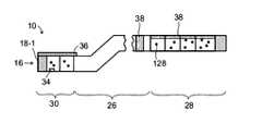
- FIGS. 1 a - 1 hillustrate an optical waveguide device 10 according to various exemplary embodiments of the present invention.
- Device 10generally has an open shape (i.e., non-tubular) such as the shape of a sheet, e.g., a planar sheet.
- device 10is a non-fiber device, i.e., not a substantially cylindrical waveguide in which a light-conducting core is surrounded by a layer of cladding, and is solid (i.e., not hollow).
- the sheetis flexible and hence may be also assume a non-planar shape. For example, when the sheet is placed on a curved surface, the sheet may acquire the curvature of the surface.
- Device 10may also have a certain degree of elasticity. Thus, one or more of the layers of device 10 may be made, for example, from an elastomer.
- device 10is substantially rigid.
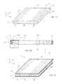
- Device 10includes a core layer 16 formed of a plurality of core structures 18 joined in, e.g., a side-by-side or nested configuration.
- Core structures 18(designated in FIGS. 1 a - 1 h by reference numerals 18 - 1 , 18 - 2 , . . . , 18 - n ) may take the form of elongated bands arranged side-by-side (see, e.g., FIG. 1 a ), or may instead have a nested configuration (see, e.g., FIG. 1 h ) with their common ends joined.
- the width of structures 18(along the x direction in FIGS. 1 a - 1 h ) may vary.
- each section of a non-planar sheetmay be described using a Cartesian x-y-z coordinate system which is rotated such that the section is tangential to the x-y plane and normal to the z direction.
- the x, y and z directionsare referred to herein as the “lateral,” “longitudinal” and “normal” directions, respectively.
- core structures 18are shown in FIGS. 1 a - 1 g as having a rectangular cross-section, this need not necessarily be the case, depending on the application.
- FIG. 1 ais a perspective view of device 10 and FIG. 1 b is a cross-sectional view along the line A-A of FIG. 1 a in embodiments in which core layer 16 is at least partially surrounded by air.
- FIG. 1 bis a cross-sectional view along the line A-A of a device similar to that illustrated FIGS. 1 a and 1 h in embodiments in which core layer 16 is at least partially surrounded by air.
- structures 18are characterized by a refractive index which is larger than the refractive index of the surrounding air.
- ⁇ x ⁇ sin ⁇ 1 (n 1 /n 2 )where n 1 and n 2 are the refractive indices of the air and the core layer, respectively, the light energy is trapped within core layer 16 and propagates therethrough via total internal reflection.
- Lightmay also propagate through device 10 when the impinging angle is smaller than the critical angle, in which case one portion of the light is emitted and the other portion thereof continues to propagate.
- the difference between the indices of refraction the core layer and surrounding airmay be selected in accordance with the desired propagation angle of the light.
- core structures 18typically include or consist essentially of a waveguide material having a refractive index greater than 1.
- waveguide materials suitable for the core structuresinclude, without limitation, a thermoplastic such as a polycarbonate, polymethyl methacrylate (PMMA), and/or polyurethane (TPU) (aliphatic) with a refractive index of about 1.50, TPU (aromatic) with a refractive index of from about 1.58 to about 1.60, amorphous nylon such as GRILAMID supplied by EMS Grivory (e.g., GRILAMID TR90 with refractive index of about 1.54), polymethylpentene, e.g., TPX supplied by Mitsui with a refractive index of about 1.46, polyvinylidene fluoride (PVDF) with a refractive index of about 1.34, or other thermoplastic fluorocarbon polymers, and/or STYROLUX (UV stabilized)
- a thermoplasticsuch as a polycarbonate, polymethyl
- FIGS. 1 c - 1 eare perspective ( FIG. 1 c ) and cross-sectional ( FIGS. 1 d and 1 e ) views along line B-B of device 10 in embodiments in which device 10 further comprises one or more cladding layers.
- the core layer of the device shown in FIG. 1 cis illustrated as having the core structures in a side-by-side configuration, this need not necessarily be the case, since, for some applications, it may be desired to have the core layer arranged in a nested configuration (e.g., the configuration schematically illustrated in FIG. 1 h ).
- device 10includes a first cladding layer 12 , a second cladding layer 14 , and core layer 16 interposed between cladding layers 12 , 14 .
- core layer 16interposed between cladding layers 12 , 14 .
- the elongated structures of core 16extend along the length of the cladding layers.
- the refractive index of the cladding layersis typically smaller than the refractive index of the core layer.
- the refractive index of the cladding layersis typically smaller than the refractive index of the core layer.
- core structures 18include or consist essentially of a waveguide material such as those identified above for the embodiment lacking cladding layers, and preferably have relatively high refractive indices.
- the indices of refractionare selected such that propagation angle is from about 2° to about 55°.
- core layer 16may be made of GRILAMID TR90 with a refractive index of about 1.54, and cladding layers 12 , 14 may be made of TPX with refractive index of about 1.46, so that ⁇ n ⁇ n 2 ⁇ n 1 ⁇ 0.08 and n 1 /n 2 ⁇ 0.948, corresponding to a propagation angle of 90° ⁇ sin ⁇ 1 (0.948), or approximately ⁇ 19°.
- a core layer 16 made of TPU (aromatic) with a refractive index of about 1.60 without claddinghas a corresponding propagation angle of 90° ⁇ sin ⁇ 1 (1/1.6), or approximately ⁇ 51°.
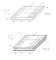
- FIGS. 1 f and 1 gare perspective views of device 10 without ( FIG. 1 f ) and with ( FIG. 1 g ) claddings, in an embodiment in which core structures 18 are in the shape of plaques (e.g., polygonal plaques such as squares or rectangles).
- plaquese.g., polygonal plaques such as squares or rectangles.
- the ordinarily skilled personwill know how to construct a cross-sectional view of these illustrations, which may be similar to FIGS. 1 b , 1 d and 1 e.
- core layer 16 into core structures 18may be accomplished by any process known in the art, such as, but not limited to, coextrusion, extrusion, coating, coinjection molding, lamination, tiling, and the like.
- core structures 18elongated or shaped as plaques
- two adjacent structuresmay be welded at their joined ends, bonded by an adhesive material disposed along their length and/or width, etc.
- a process for forming core layer 16 according to some embodiments of the present inventionis provided below.
- some of the core structuresinclude additives selected to provide the individual core structures with a predetermined effective refractive index.
- the effective refractive indexdepends on the type and concentration of the additive. Typically, higher additive concentrations provide higher effective refractive indices.
- the additivesmay take the form of light-scattering particles 20 embedded in one or more of the core structures. In various exemplary embodiments of the invention, the size, concentration, refractive index, and/or type of light-scattering particles 20 varies among at least two of the core structures.
- Particles 20are dispersed within core structures 18 and facilitate emission of the light from a surface 23 of core layer 16 and/or a surface 24 of cladding layer 14 (in the embodiments in which cladding layer 14 is employed). Particles 20 serve as scatterers and typically scatter optical radiation in more than one direction. When light is scattered by a particle 20 such that the impinging angle is below the critical angle, no total internal reflection occurs and the scattered light is emitted through surface 23 and/or surface 24 .
- the light-scattering particlesmay be beads, e.g., glass beads, or other ceramic particles, rubber particles, silica particles, particles including or consisting essentially of inorganic materials such as BaSO 4 or TiO 2 , particles including or consisting essentially of a phosphor material (as further described below), and the like.
- the light-scattering particlesare substantially or even completely non-phosphorescent. Such non-phosphorescent particles merely scatter light without converting the wavelength of any of the light striking the particles.
- the term “light-scattering particles”may also refer to non-solid objects embedded in the waveguide material from which core structure are made, provided that such objects are capable of scattering the light.
- suitable non-solid objectsinclude, without limitation, closed voids within the core structures, e.g., air bubbles, and/or droplets of liquid embedded within the core structures.
- the light-scattering particlesmay also be organic or biological particles, such as, but not limited to, liposomes.
- optical elementssuch as microlenses are utilized in conjunction with, or even instead of, light-scattering particles.
- optical elementsinclude or consist essentially of structures such as hemispheres or diffusive dots. In such embodiments, the optical elements function to out-couple light propagating through device 10 .
- “optical elements”may generically refer to elements such as microlenses as well as light-scattering particles, e.g., non-photoluminescent particles.
- the concentration, size and/or type of particlesis selected such as to provide illumination at a predetermined profile (e.g., intensity profile) from predetermined regions of surface 23 or 24 .
- a predetermined profilee.g., intensity profile
- the concentration of particles 20may be large and/or the particles may have a type and/or size which provides them with high scattering properties; in regions where a smaller portion of the light is to be emitted the concentration of particles 20 may be smaller and/or the particles may have a type and/or size which provides them with lower scattering properties; and in surface regions from which no light is to be emitted, substantially no particles are embedded in core structures 18 .
- the energy trapped in waveguide device 10decreases each time a light ray is emitted through surface 23 or 24 .
- device 10may be desired to use device 10 to provide a uniform surface illumination.
- a uniform surface illuminationmay be achieved by gradually increasing the ratio between the emitted light and the propagated light.
- the increasing ratio of emitted light to propagated lightis achieved by an appropriate selection of the distribution, type, refractive index, and/or size of particles 20 in the core layer 16 .
- the concentration of particles 20may be an increasing function of the optical distance traversed by the propagated light.
- the optical output at specific and predetermined regionsmay be controlled by arranging the core structures 18 such that different core structures have different concentrations, sizes, refractive indices, and/or types of particles 20 .
- the core structures 18are arranged to define a first zone 26 and a second zone 28 .
- First and second zones 26 , 28may include portions of core layer 16 such that a profile of an optical mean free path characterizing core layer 16 is generally flat across the first zone 26 and monotonically varying across the second zone 28 .
- the optical mean free pathmay be measured directly by positioning a bulk material in front of a light-emitting element and measuring the optical output through the bulk at a given direction as a function of the thickness of the bulk.
- a bulk material, t mm in thicknessreduces the optical output of a light source at the forward direction by 50%, the material is said to have a mean free path of t mm.
- FIG. 2 ashows a representative example of an optical mean free path as a function of the lateral direction x.
- the optical mean free pathis substantially constant in zone 26 , and is a decreasing function of x in zone 28 .
- the decrement of the optical mean free path in region 28facilitates an increasing ratio between the emitted portion and propagated portions of the light.
- Zone 26may include one or more core structures and is typically devoid of light-scattering particles 20 .
- zone 26propagates light with minimal or no emissions from surfaces 23 or 24 , i.e., zone 26 is a propagation region.
- Zone 28may include a plurality, e.g., three or more, of core structures 18 each having particles 20 embedded therein.
- zone 28provides illumination by out-coupling light from core 16 (i.e., zone 28 is an out-coupling region for light propagated through zone 26 ).
- the brightness of the illumination from zone 28may be substantially uniform.
- Brightness uniformitymay be calculated by considering the luminance deviation across the range of azimuthal angles as a fraction of the average luminance across that range.
- substantially uniform brightnessrefers to a BU value which is at least 0.8 when calculated according to the above formula.
- the value of BUis at least 0.85, more preferably at least 0.9, and still more preferably at least 0.95.
- the concentration of particles 20 in the core structures 18 of zone 28may be an increasing function of the distance from zone 26 .
- the type and/or size of the particles in the individual core structures 18 of zone 28may vary to achieve the desired profile.
- the concentration, type, size, and/or refractive index of particles 20 in zone 28may change in a direction of light propagation through device 10 (denoted as the x direction in FIG. 1 b ).
- the concentration, type, size, and/or refractive index of particles 20may be substantially constant in at least one of the directions perpendicular to the light-propagation direction (e.g., the y and z directions in FIG. 1 b ).
- each core structure 18 in zone 28may have a substantially constant concentration, type, size, and/or refractive index of particles 20 therewithin, but this value may change in at least one (or every) other core structure 18 in zone 28 .
- third zone 30may be proximate or in direct contact with first zone 26 and away from second zone 28 .
- Third zone 30may comprise or consist essentially of one or more core structures 18 having light-scattering particles 20 embedded therein.
- FIG. 2 bA representative example of an optical mean free path in the embodiment in which three zones are defined is illustrated in FIG. 2 b.
- Zone 30may be an in-coupling region for facilitating the entry of light into device 10 .
- Light enters device 10 at zone 30propagates through zone 26 and exits (i.e., is out-coupled) at zone 28 .
- One or more of the core structures 18typically the first and last structures (i.e., structures 18 - 1 and 18 - n in the illustration of FIG. 1 d ) may be made light-reflective so as to prevent or reduce optical losses through the side(s) of device 10 .
- the characteristic refractive index of such light-reflective core structures 18is preferably above 2.
- a representative example of a material having a sufficiently high refractive index suitable for the present embodimentis TiO 2 , which has a refractive index of about 2.5.
- light-reflective structures 22may be disposed proximate the entire height of device 10 as shown in FIG. 1 e.
- Coupling of light into device 10may be facilitated using an optical funnel 32 positioned adjacent to layer 12 or layer 16 at zone 30 .
- Funnel 32is preferably configured to receive light from one or more light-emitting elements and to transmit the light into layer 12 or layer 16 .
- the principle of operation of funnel 30 according to some embodiments of the present inventionis further detailed herein under with reference to FIG. 4 .
- device 10may further include one or more light reflectors 36 adjacent to cladding layer 14 at the region of cladding layer 14 which overlaps zone 30 .
- Reflector(s) 36reduce illumination in any direction other than a circumferential direction.
- zone 30 of device 10includes one or more components that cause the light exiting zone 30 (into zone 26 ) to have a predetermined optical profile, such as, but not limited to, a substantially uniform color profile or substantially uniform white light.
- This embodimentmay be implemented by color mixing, optical means, or may be implemented via luminescence, a phenomenon in which energy is absorbed by a substance, commonly called a luminescent, and is emitted in the form of light. The wavelength of the emitted light differs from the characteristic wavelength of the absorbed energy (the characteristic wavelength equals hc/E, where h is the Plank's constant, c is the speed of light and E is the energy absorbed by the luminescent).
- Luminescenceis a widely occurring phenomenon which may be classified according to the excitation mechanism as well as according to the emission mechanism. Examples of such classifications include photoluminescence and electroluminescence. Photoluminescence is sub-classified to fluorescence and phosphorescence.
- a photoluminescentis generally a material which absorbs energy is in the form of light.
- a fluorescent materialis a material which emits light upon return to the base state from a singlet excitation
- a phosphorescent materialsis a material which emits light upon return to the base state from a triplet excitation.
- fluorescent materials, or fluorophoresthe electron de-excitation occurs almost spontaneously, and the emission ceases when the source of the energy exciting the fluorophore is removed.
- phosphor materials, or phosphorsthe excitation state involves a change of spin state, which decays only slowly. In phosphorescence, light emitted by an atom or molecule persists after the excitation source is removed.
- Photoluminescent materialsare used according to various embodiments of the present invention for altering the color of light. Since blue light has a short wavelength (compared, e.g., to green or red light), and since the light emitted by a photoluminescent material has a longer wavelength than the absorbed light, blue light generated by a blue light-emitting element such as a light-emitting diode (LED) may be readily converted to visible light having a longer wavelength. Accordingly, in various exemplary embodiments of the invention a specific light profile on the exit of light into zone 26 is provided using one or more photoluminescent layers disposed on or embedded in device 10 .
- a blue light-emitting elementsuch as a light-emitting diode (LED)
- photoluminescent layeris commonly used herein to describe one photoluminescent layer or a plurality of photoluminescent layers. Additionally, a photoluminescent layer may include one or more types of photoluminescent species.
- a photoluminescent layeris characterized by an absorption spectrum (i.e., a range of wavelengths of light absorbed by the photoluminescent molecules to effect quantum transition to a higher energy level) and an emission spectrum (i.e., a range of wavelengths of light emitted by the photoluminescent molecules as a result of quantum transition to a lower energy level).
- the emission spectrum of the photoluminescent layeris typically wider and shifted relative to its absorption spectrum. The difference in wavelength between the apex of the absorption and emission spectra of the photoluminescent layer is referred to as the Stokes shift of the photoluminescent layer.
- the absorption spectrum of the photoluminescent layerpreferably overlaps, at least partially, the emission spectrum of the light source which feeds device 10 . More preferably, for each characteristic emission spectrum of the light source, there is at least one photoluminescent layer having an absorption spectrum overlapping the characteristic emission spectrum. According to some embodiments of the present invention, the apex of the source's emission spectrum lies in the spectrum of the photoluminescent layer, and/or the apex of the photoluminescent layer's absorption spectrum lies in the spectrum of the light source.
- the photoluminescent layermay “convert” the wavelength of a portion of the light emitted by the light source. More specifically, for each photon which is successfully absorbed by the layer, a new photon is emitted. Depending on the type of photoluminescent, the emitted photon may have a wavelength which is longer or shorter than the wavelength of the absorbed photon. Photons which do not interact with the photoluminescent layer propagate therethrough. The combination of converted light and non-converted light forms the profile of light entering zone 26 . This “mixed” light is preferably spectrally different from each of the converted light and the non-converted light. Since the mixed light is formed by the superposition of the converted light and the non-converted light, the spectrum of the mixed light generally contains all of the wavelengths of the converted light and the non-converted light.
- the photoluminescent materialis disposed neither on an outer surface of device 10 nor directly on a light-emitting element 34 . Rather, as described further below, the photoluminescent material (e.g., in the form of particles and/or a layer or layers) is disposed within device 10 some distance away from light-emitting element 34 .
- FIGS. 3 a - dare fragmentary schematic illustrations of device 10 showing a cross-section of zone 30 parallel to the z-x plane. Several components of device 10 are omitted from FIGS. 3 a - d for clarity of presentation.
- FIG. 3 aillustrates an embodiment in which the elongated structures at the ends of zone 30 (structures 18 - 1 and 18 - 3 , in the present example) include or consist essentially of photoluminescent material, e.g., a phosphor or a fluorophore.
- FIG. 3 billustrates an embodiment in which one or more of the inner elongated structures of zone 30 (structure 18 - 2 , in the present example) include or consist essentially of photoluminescent material.
- FIG. 3 aillustrates an embodiment in which the elongated structures at the ends of zone 30 (structures 18 - 1 and 18 - 3 , in the present example) include or consist essentially of photoluminescent material, e.g., a
- 3 cis a schematic illustration of an embodiment in which a photoluminescent layer 38 , which may include or consist essentially of a photoluminescent material such as a phosphor or a fluorophore, is disposed on the surface of layer 12 and/or layer 14 .
- the wavelength of the lightis changed via the multiple impingements of the light on surface of layer 12 and/or 14 .
- only one of the surfacesis coated by the photoluminescent layer 38 .
- the surface of layer 14may be coated by the photoluminescent layer 38 and the surface of layer 12 may be left exposed for better light coupling between layer 12 and the light-emitting element or funnel 32 .
- Photoluminescent materialmay also be incorporated in the form of particles, as illustrated in FIG. 3 d .
- a plurality of photoluminescent particles 128may be distributed within one or more of the core structures 18 in accordance with the desired light output profile.
- the particles 128are uniformly distributed in all the core structures 18 .
- the particlesare distributed such that there are core structures 18 with a higher population of the particles 128 and core structures 18 with a lower population of the particles 128 , depending on the desired profile in or near each core structure.
- FIG. 4 aA cross-sectional view of an exemplary embodiment of optical funnel 32 is illustrated in FIG. 4 a .
- Optical funnel 32receives the light from one or more light-emitting elements 34 and distributes it prior to entry of the light into layer 12 (not shown in FIG. 4 , see FIGS. 1 d and 1 e ) so as to establish a plurality of entry locations within zone 30 (hence improving the uniformity of light distribution within zone 30 ).
- Light-emitting elements 34may be arranged near funnel 32 or they may be embedded in funnel 32 . Efficient optical transmission between funnel 32 and layer 12 is preferably ensured by impedance matching therebetween.
- Each light-emitting element 34may be a discrete light source, e.g., an LED.
- each light-emitting element 34is a substantially unpackaged (or “bare”) LED die.
- funnel 32 or other portions of device 10function as the “package” for light-emitting element 34 .
- bare LED diesdo not include a phosphor or other photoluminescent material as a portion thereof (e.g., on a common substrate therewith or incorporated into or onto the LED semiconductor layer structure).
- a single light-emitting element 34is described herein, more than one light-emitting element 34 could generally also be utilized, and vice versa.
- lightis emitted from light-emitting element 34 upon supply of electrical current thereto.
- Funnel 32may be made as a surface-emitting waveguide or surface-emitting optical cavity which receives the light generated by light-emitting elements 34 through an entry surface 142 , distributes it within an internal volume 148 , and emits it through an exit surface 144 , which is typically opposite to the entry surface 142 .
- funnel 32comprises one or more light reflectors 146 , which are typically arranged peripherally about volume 148 so as to form an optical cavity or an optical resonator within volume 148 .
- One or more light reflectors 146may also be formed on or attached to the entry surface 142 of funnel 32 .
- one or more openings 150are formed on the reflectors 146 at the entry surface, thus allowing light to enter volume 148 . Openings 150 may be substantially aligned, e.g., in the x-y plane, with light-emitting elements 34 .
- Funnel 32may include or consist essentially of a waveguide material, or it may be filled with a medium having a small absorption coefficient to the spectrum or spectra emitted by the light-emitting elements 34 .
- funnel 32may be filled with air, or be made of a waveguide material which is similar or identical to the material of the cladding layers 12 and/or 14 .
- the advantage of using airis its low absorption coefficient, and the advantage of a waveguide material identical to material of the cladding layers 12 , 14 is impedance matching therewith.
- funnel 32When funnel 32 is filled with medium having a small absorption coefficient (e.g., air), there may be no impedance matching at exit surface 144 of funnel 32 . Thus, some reflections and refraction events may occur upon the impingement of light on the interface between funnel 32 and the cladding layer 12 . Neither refraction nor reflection events cause significant optical losses; refraction events contribute to the distribution of light within zone 30 , and reflection events contribute to the distribution of light within volume 148 .
- medium having a small absorption coefficiente.g., air
- funnel 32is supplemented by photoluminescent material for controlling the output profile of the light, as schematically illustrated in FIGS. 4 b - 4 d .
- the reflectors 146are not shown in FIGS. 4 b - 4 d .
- funnel 32may include one or more light reflectors 146 as detailed above.
- a photoluminescent layer 38is interposed between layer 12 and funnel 32 ; in the embodiment illustrated in FIG. 4 c , photoluminescent layer 38 is embedded in funnel 32 ; and in the embodiment illustrated in FIG. 4 d a plurality of photoluminescent particles 128 is distributed within funnel 32 .
- Various embodiments of the present inventionfeature one or more light-emitting elements 34 embedded within zone 30 of device 10 and/or photoluminescent material (e.g., photoluminescent layer 38 and/or particles 128 ) disposed within device 10 outside of the direct “line-of-sight” from light-emitting elements 34 . That is, in such embodiments, there is no direct, straight-line optical path between the light-emitting elements 34 and the photoluminescent material; rather, light emitted from light-emitting elements 34 reflects from a reflector, a surface, or an interface within device 10 before reaching the photoluminescent material.
- photoluminescent materiale.g., photoluminescent layer 38 and/or particles 128
- any light striking and being back-reflected from the photoluminescent materialwill not propagate directly back into light-emitting element 34 (where it could be absorbed, thus reducing overall light output and efficiency of device 10 ). Rather, light reflecting from the photoluminescent material will tend to remain within device 10 and eventually reflected back toward zone 28 to be out-coupled.
- there is substantially no direct line-of-sight between light-emitting element 34 and the photoluminescent materiali.e., less than approximately 5% of the light from light-emitting element 34 has a direct line-of-sight to the photoluminescent material; any losses thereof are therefore negligible.
- the photoluminescent materialmay advantageously be located remotely in relation to light-emitting element 34 , i.e., it may be present in zone 26 and/or zone 28 rather than proximate light-emitting element 34 (in zone 30 or in funnel 32 , for example).
- the quantum efficiency (or other performance metric) of the photoluminescent materialmay degrade when the material is exposed to elevated temperatures, e.g., temperatures greater than approximately 50° C. Remote placement of the photoluminescent material prevents the temperature of the material from rising during operation due to, e.g., heat given off by light-emitting element 34 .
- the temperature of remotely placed luminescent materialwill generally remain at the ambient temperature of the surroundings of device 10 .
- the temperature of the luminescent materialmay remain at least approximately 30° C., or even at least 100° C. less than the temperature of light-emitting element 34 during operation.
- elevated temperatures capable of damaging (e.g., degrading the quantum efficiency of) the photoluminescent materialare often required when affixing or embedding light-emitting element 34 into device 10 .
- Remote placement of the photoluminescent materialenables the photoluminescent material to be provided within device 10 prior to the addition of light-emitting element 34 —the distance therebetween prevents the elevated temperatures from damaging the photoluminescent material.
- a remotely placed photoluminescent materialmay be located in any one or more of a variety of locations, as depicted in FIGS. 4 e - 4 j .
- FIG. 4 edepicts a photoluminescent layer 38 within zone 26 and outside the direct line-of-sight of light-emitting element(s) in funnel 32 (e.g., as illustrated in FIG. 4 a ). At least a portion of the light propagating through zone 26 is converted by photoluminescent layer 38 to light of a different wavelength, and then the converted and unconverted light components enter zone 28 where they are out-coupled together to form, e.g., substantially white light. In this and similar configurations, the propagating light converted by the photoluminescent material travels in a direction substantially perpendicular to the direction of the eventual out-coupled light. Such configurations may enable superior uniformity, brightness, and color of the out-coupled light.
- FIG. 4 fdepicts potential locations in zone 28 for the photoluminescent material, which are also outside the direct line-of-sight of light-emitting element(s) in funnel 32 .
- photoluminescent particles 128may be utilized in conjunction with (or instead of) particles 20 ; at least a portion of light striking particles 128 is converted to light of a different wavelength, and the light out-coupled from zone 28 is, e.g., substantially white.
- photoluminescent layer 38may be disposed within zone 28 , e.g., proximate a top edge thereof. In this configuration, at least a portion of the light already being out-coupled (i.e., on its way out of device 10 ) is converted to light of a different wavelength.
- the exiting converted and unconverted lightmix to form, e.g., substantially white light.
- the uniformity of the light striking the photoluminescent materialmay be greater than the uniformity of the light striking particles 20 . That is, the scattering by particles 20 increases the uniformity of the light, which then strikes the photoluminescent material and is out-coupled from device 10 with a high level of uniformity.
- the line of sight between light-emitting element 34 and the photoluminescent materialmay not be eliminated by placement of particles 20 therebetween, as some light may propagate through the region populated with particles 20 without being scattered thereby.
- FIG. 4 gdepicts possible locations for a photoluminescent material described with reference to FIGS. 4 e and 4 f , any of which (or any combination of which) may be utilized in conjunction with a device 10 shaped to eliminate the direct line-of-sight between the light-emitting element(s) in funnel 32 and photoluminescent layer 38 and/or particles 128 .
- device 10may include a bend, curve, or other geometry in zone 26 (or even in zone 28 ) which facilitates the elimination of a direct line-of-sight between the light-emitting element(s) and the photoluminescent material.
- This geometrymay also facilitate subsequent “tiling” of multiple devices 10 to form an illumination panel, e.g., a panel in which the zones 28 of devices 10 overlie zones 26 and/or 30 of adjacent devices 10 (as further described below with reference to FIGS. 12 a and 12 b ).
- the shape depicted in FIG. 4 gis exemplary, and many other configurations are possible.
- FIGS. 4 h - 4 jare analogous to FIGS. 4 e - 4 g , respectively, but depict one or more light-emitting elements 34 embedded within device 10 (here shown embedded within a core structure 18 of zone 30 ) rather than coupled to device 10 via funnel 32 .
- zone 26may be elongated and/or be sized and shaped so as to substantially or completely eliminate the direct line-of-sight between light-emitting element(s) 34 and photoluminescent layer 38 and/or particles 128 .
- Each device 10 depicted in FIGS. 4 e - 4 jmay also incorporate cladding layers 12 , 14 , e.g., as illustrated in FIGS. 1 c - 1 e.
- light from light-emitting element 34(whether embedded within device 10 or operated in conjunction with funnel 32 ) generally enters zone 30 in an “in-coupling direction,” i.e., along the z axis indicated in FIG. 1 b .
- the lightOnce in-coupled into device 10 by scattering from particles 20 and/or reflector 36 , the light generally propagates through device 10 (e.g., through zone 26 ) in a “propagation direction” that is substantially perpendicular to the in-coupling direction. As illustrated in FIG. 1 b , the propagation direction is generally along the x axis.
- the lightAfter the light enters zone 28 , it is generally out-coupled from device 10 (i.e., emitted from surface 23 and/or 24 ) in an “out-coupling direction” that is substantially perpendicular to the propagation direction (e.g., along the z axis indicated in FIG. 1 b ).
- the in-coupling direction and the out-coupling directionmay be substantially parallel.
- at least a portion of the light propagating in device 10 in the propagation directionis stimulated by photoluminescent layer 38 and/or particles 128 , giving rise to the mixed light that is out-coupled from device 10 in an out-coupling direction substantially perpendicular to the propagation direction.
- This configurationmay enable better brightness and/or color uniformity than devices in which stimulated light (i.e., light before or as it strikes a photoluminescent material) propagates in a direction that is not substantially perpendicular (e.g., a substantially parallel direction) to an out-coupling direction of the mixed light resulting from stimulation by the photoluminescent material.
- stimulated lighti.e., light before or as it strikes a photoluminescent material
- a direction that is not substantially perpendiculare.g., a substantially parallel direction
- Phosphorsare widely used for coating individual LEDs, typically to obtain white light therefrom.
- photoluminescent layers incorporated in waveguide devices as described hereinhave not been employed.
- the advantage of providing photoluminescent layer 38 and/or particles 128 (in layer 16 and/or funnel 32 ) as opposed to on each individual light-emitting element,is that waveguide device 10 diffuses the light before emitting it.
- photoluminescent layer 38 and/or particles 128collects light having a predetermined extent. This configuration allows a better control on the light profile provided by device 10 .
- phosphorescent and fluorescent substanceare contemplated. Representative examples include, without limitation, the phosphors disclosed in U.S. Pat. Nos. 5,813,752, 5,813,753, 5,847,507, 5,959,316, 6,155,699, 6,351,069, 6,501,100, 6,501,102, 6,522,065, 6,614,179, 6,621,211, 6,635,363, 6,635,987, 6,680,004, 6,765,237, 6,853,131, 6,890,234, 6,917,057, 6,939,481, 6,982,522, 7,015,510, 7,026,756, 7,045,826, and 7,005,086, the entire disclosures of which are hereby incorporated by reference.
- the quantum efficiency of photoluminescent layer 38 and/or particles 128is only stable up to a temperature of approximately 50° C. However, in many configurations the temperature of such materials remains lower than this level due to spatial separation of photoluminescent layer 38 and/or particles 128 from the light-emitting element(s).
- layer 38 and/or particles 128include or consist essentially of one or more electroluminescent materials rather than (or in addition to) photoluminescent materials.
- electroluminescent materialsmay include or consist essentially of quantum dot materials and/or organic LED (OLED) materials.
- Suitable quantum dotsmay include or consist essentially of cadmium selenide.
- photoluminescent layer 38complements the light emitted by light-emitting elements 34 to create a white light, e.g., using dichromatic, trichromatic, tetrachromatic or multichromatic approach.
- blue-yellow dichromatic approachmay be employed, in which case blue light-emitting elements (e.g., InGaN LEDs with a peak emission wavelength at about 460 nm) are used, and photoluminescent layer 38 may include or consist essentially of phosphor molecules with an absorption spectrum in the blue range and an emission spectrum extending to the yellow range (e.g., cerium-activated yttrium aluminum garnet, or strontium silicate europium).
- blue light-emitting elementse.g., InGaN LEDs with a peak emission wavelength at about 460 nm
- photoluminescent layer 38may include or consist essentially of phosphor molecules with an absorption spectrum in the blue range and an emission spectrum extending to the yellow range (e.g., cerium-activated yttrium aluminum garnet, or strontium silicate europium).
- the blue light generated by the blue light-emitting elements 34is efficiently diffused in the waveguide material before interacting with photoluminescent layer 38 and/or particles 128 .
- Layer 38 and/or particles 128emit light in its emission spectrum and complement the blue light which is not absorbed by photoluminescent layer 38 and/or particles 128 to white light.
- ultraviolet light-emitting elementse.g., LEDs of GaN, AlGaN, and/or InGaN with a peak emission wavelength between 360 nm and 420 nm
- Light of such ultraviolet light-emitting elementsis efficiently diffused in the waveguide material.
- two photoluminescent layers 38 and/or two types of photoluminescent particles 128are preferably employed.
- One such photoluminescent layer and/or type of particlesmay be characterized by an absorption spectrum in the ultraviolet range and emission spectrum in the orange range (with peak emission wavelength from about 570 nm to about 620 nm), and another photoluminescent layer and/or type of particles may be characterized by an absorption spectrum in the ultraviolet range and emission spectrum in the blue-green range (with peak emission wavelength from about 480 nm to about 500 nm).
- the orange light and blue-green light emitted by the two photoluminescent layers 38 and/or two types of photoluminescent particles 128blend to appear as white light to an observer. Since the light emitted by the ultraviolet light-emitting elements is above or close to the end of the visual range, it is not discerned by the observer.
- two photoluminescent layers 38When two photoluminescent layers 38 are employed, they may be deposited one on top of the other so as to improve the uniformity. Alternatively, a single photoluminescent layer 38 having two types of photoluminescent material with the above
- a trichromatic approachis employed.
- blue light-emitting elementsmay be employed as described above, with two photoluminescent layers 38 and/or two types of photoluminescent particles 128 .
- a first photoluminescent layer 38 and/or type of photoluminescent particles 128may include or consist essentially of phosphor molecules with an absorption spectrum in the blue range and an emission spectrum extending to the yellow range as described above, and a second photoluminescent layer 38 and/or type of photoluminescent particles 128 may include or consist essentially of phosphor molecules with an absorption spectrum in the blue range and an emission spectrum extending to the red range (e.g., cerium-activated yttrium aluminum garnet doped with a trivalent ion of praseodymium, or europium-activated strontium sulphide).
- the unabsorbed blue light, the yellow light, and the red light blendto appear as white light to an observer.
- a configurationis which light-emitting elements 34 with different emission spectra are employed and several photoluminescent layers 38 are deposited and/or several types of photoluminescent particles 128 are distributed, such that the absorption spectrum of each photoluminescent layer 38 and/or type of photoluminescent particles 128 overlaps one of the emission spectra of the light-emitting elements 34 , and all the emitted colors (of the light-emitting elements 34 and the photoluminescent layers 38 and/or particles 128 ) blend to appear as white light.
- the advantage of such a multi-chromatic configurationis that it provides a high-quality white balance because it allows better control of the various spectral components of the light in a localized manner, e.g., along an edge or surface of device 10 .
- the color composite of the white output lightdepends on the intensities and spectral distributions of the emanating light emissions. These depend on the spectral characteristics and spatial distribution of the light-emitting elements 34 , and, in the embodiments in which one or more photoluminescent components (layers 38 and/or particles 128 ) are employed, on the spectral characteristics of the photoluminescent components and on the amount of unabsorbed light.
- the amount of light unabsorbed by the photoluminescent componentsis, in turn, a function of the characteristics of the components, e.g., thickness of the photoluminescent layer(s) 38 , density of photoluminescent material(s), and the like.
- device 10may provide substantially uniform white light.
- the “whiteness” of the lightmay be tailored according to the specific application for which device 10 is intended.
- the spectral components of the light provided by device 10may be selected in accordance with the spectral characteristics of the color filters of the liquid crystal panel.
- the white light provided by device 10includes at least at the distinct colors of such filters. This configuration significantly improves the optical efficiency as well as the image quality provided by the LCD device, because the optical losses due to mismatch between the spectral components of the backlight unit and the color filters of the liquid crystal panel are reduced or eliminated.
- the emission spectra of the light-emitting elements 34are preferably selected to substantially overlap the characteristic spectra of the color filters of an LCD panel.
- the emission spectra of the photoluminescent components and optionally the emission spectrum (or spectra) of the light-emitting elementsare preferably selected to overlap the characteristic spectra of the color filters of an LCD panel.
- the overlap between a characteristic emission spectrum and a characteristic filter spectrumis about 70% spectral overlap, more preferably about 80% spectral overlap, and even more preferably about 90%.
- the followingis a description of a production process for the core layer 16 and the optical waveguide device 10 according to various exemplary embodiments of the present invention.
- the core layeris formed by coextrusion.
- coextrusionrefers to the process of simultaneous extrusion of several die outputs which are welded together before chilling to form an extrudate having an open shape, e.g., a non-tubular sheet.
- An extrudate formed by a coextrusion process according to some embodiments of the present inventionmay be a single-layer structure or a laminate structure having two or more layers.
- the coextrusion processis employed in an extrusion coating process in which an extrudate formed by the coextrusion process is applied so as to coat one or more existing layers.
- a plurality of light-transmissive compositions in a molten or plastic statemay be coextruded to form the elongated core structures of core layer 16 .
- Each light-transmissive compositionmay be extruded to form a single core structure 18 , and may be a polymeric material mixed with light-scattering particles of type, size and concentration selected to provide the core structure 18 with the desired optical properties (e.g., mean free path).
- a coextrusion apparatus 50which may be used according to some embodiments of the present invention is schematically illustrated in FIG. 5 .
- the melt streamscomprise light-transmissive compositions in accordance with the respective core structures 18 to be formed.
- Extruders 54discharge the compositions, which are conveyed by conventional conduits (not shown) to a coextrusion die or feedblock 56 .
- Die 56combines and arranges the compositions and issues a composite flat stream 58 in which the various compositions flow side-by-side.
- a chill roller system 60quenches stream 58 to form core layer 16 which includes or consists essentially of a plurality of core structures 18 as described above.
- the formed core structures 18may have any shape or cross-section, e.g., rectangular or triangular.
- One or more of the extruded core structures 18may be made reflective. This may be achieved by judicious selection of the composition from which these core structures are formed.
- a composition characterized by high refractive indexe.g., 2 or more
- a representative example of a material having a sufficiently high refractive index for reflectivityis TiO 2 , which has a refractive index of about 2.5.
- TiO 2which has a refractive index of about 2.5.
- Coextrusion apparatus 50may be adapted to simultaneously form the core layer 16 as well as the cladding layers 12 , 14 .
- This approachis illustrated in FIG. 6 , which shows apparatus 50 with a die 56 configured to combine and arrange the compositions into a laminated flat stream 58 in which the intermediate layer of stream 58 is composed of side-by-side flow of the various compositions of the core layer 16 and the outer layers of the stream are composed of the compositions of the cladding layers 12 , 14 .
- additional layersare formed above and below the cladding layers 12 , 14 , e.g., for the purpose of protecting or reinforcing the cladding layers 12 , 14 .
- apparatus 50performs an extrusion coating process, whereby the core structures 18 of core layer 16 are coextruded on a cladding layer 12 which is already in a dimensionally stable (i.e., rigid) state.
- cladding layer 14may optionally be laminated on core layer 16 to form a three-layer structure.
- the layer(s)may be further treated while the compositions are in molten or plastic state.
- One example of such treatmentis application of heat and/or pressure so as to at least partially mix respective compositions at common edges of adjacent core structures 18 .
- the heat and/or pressure treatmentmay result in a concentration gradient across the lateral direction of the core structures 18 . This embodiment is particularly useful when it is desired to have a smooth profile along the optical mean free path.
- Post-extrusion treatment of the formed core structures 18may be performed by roller system 60 (prior to the cooling of the extruded structures), or it may be done using another roller system.
- the post-extrusion treatmentmay be performed after the structures are cooled.
- the post-extrusion treatmentmay include reheating of the core structures.
- the optical waveguide device featured in embodiments of the present inventionmay also be manufactured by a lamination process. Suitable lamination processes may be employed on both thermoset and thermoplastic materials. Any lamination technique suitable for the materials from which core layer 16 and cladding layers 12 , 14 are formed may be employed.
- the lamination processmay be executed with or without a solid support.
- a solid supporte.g., a metal support or other rigid support
- itis preferably designed and constructed to allow lamination of individual core structures 18 in a side-by-side fashion.
- the solid supportpreferably fixes each individual core structure 18 to its place sidewise with a previously laminated elongated structure.
- FIGS. 8 a - 8 cA lamination technique according to various embodiments is schematically illustrated in FIGS. 8 a - 8 c .
- the processstarts with a substrate 62 ( FIG. 8 a ), on which the lamination process is executed.
- the processcontinues with the lamination of a plurality of core structures 18 (e.g., elongated core structures) in a side-by-side configuration on a substrate 62 to form core layer 16 ( FIG. 8 b ).
- the laminationmay be performed by heat-and-press, with or without adhesives.
- substrate 62may serve as a cladding layer (e.g., layer 12 of FIGS. 1 c - 1 e or 1 g ).
- substrate 62preferably includes or consists essentially of a flexible cladding material and is preferably laid on a support substrate (not shown), which is desirably planar.
- One or more light-reflective structuresmay be laminated sidewise relative to core layer 16 . This may be done in a similar manner to the lamination of the other core structures 18 .
- the core structures 18may be joined at their common ends using any technique known in the art, including, without limitation, adhesive bonding, solvent bonding, or welding (also known as fusion bonding).
- the lamination of core 16 on substrate 62may be preceded by a step in which an adhesive optical material is applied on substrate 62 . If desired, substrate 62 may be removed following the lamination of the core structures 18 . It this embodiment, the air serves as the “cladding” layer as detailed above.
- the processcontinues by laminating cladding layer 14 on core layer 16 ( FIG. 8 c ).
- an optical adhesivemay be applied on core layer 16 prior to the lamination of cladding layer 14 thereon.
- FIGS. 9 a - 9 cAn additional technique for fabricating device 10 is illustrated in FIGS. 9 a - 9 c .
- the processstarts with substrate 62 ( FIG. 9 a ).
- a plurality of core structures 18 having the shape of plaquesare tiled in a side-by-side configuration on a substrate 62 to form core layer 16 ( FIG. 9 b ).
- the tilingmay be performed by lamination techniques such as heat-and-press, with or without adhesives.
- substrate 62may serve as a cladding layer (e.g., layer 12 of FIGS. 1 c - e or 1 g ).
- substrate 62is made of a flexible cladding material and is preferably laid on a support substrate (not shown), which is preferably planar.
- One or more light-reflective structuresmay be laminated sidewise relative to core layer 16 . This may be done in a similar manner to the lamination of the other core structures 18 .
- the core structures 18may be joined at their common ends using any technique known in the art, including, without limitation, adhesive bonding, solvent bonding, or welding.
- the lamination of core 16 on substrate 62may be preceded by a step in which an adhesive optical material is applied on substrate 62 .
- substrate 62may be removed following the lamination of the core structures 18 .
- the airserves as the “cladding” layer as detailed above.
- the processcontinues by laminating cladding layer 14 on core layer 16 ( FIG. 9 c ).
- an optical adhesivemay be applied on core layer 16 prior to the lamination of cladding layer 14 thereon.
- one or more additional layersmay be attached to cladding layers 12 and/or 14 .
- Thismay be achieved using any procedure known in the art, including, without limitation, printing, embossing, lamination, and the like.
- the attachment of the additional layersmay be performed using any technique, including, without limitation, adhesive bonding, solvent bonding, welding, mechanical fastening, co-consolidation, and the like.
- the additional layermay cover the entire surface area of the cladding or a portion thereof.
- a reflective foil 36see, e.g., FIG. 1 a
- jacket layersfor protecting the cladding layers 12 , 14 .
- FIGS. 10 a - 10 cAn additional technique for fabricating device 10 according to some embodiments of the present invention is illustrated in FIGS. 10 a - 10 c .
- co-injection moldingis employed.
- Co-injection moldingis a variant of a process known as injection molding.
- thermoplastic polymers or the likeare fed from a hopper into a barrel, melted by a reciprocating screw and/or electric heat, and are propelled forward by a ram (piston, plunger) or the screw (used as a plunger) into a mold cavity, which is cooled to below the heat-distortion temperature of the resin.
- Co-injection moldingtakes advantage of a characteristic of injection molding called fountain flow.
- the material at the melt frontmoves from the center line of the stream to the cavity walls.
- the wallsare typically kept below the transition temperature of the melt such that the material that touches the walls cools rapidly and freezes in place. This provides insulating layers through which new melt makes its way to the melt front.
- the co-injection techniqueis employed for forming a core layer 16 having a plurality of core structures 18 in a nested configuration.
- a co-injection molding system suitable for the present embodimentsis illustrated in FIG. 10 a .
- the systemtypically includes a co-injection manifold 230 mounted relative to a mold cavity 220 , and shaped according to the desired shape of the device.
- mold cavity 220has a substantially planar shape.
- Manifold 230includes a nozzle housing 234 having forward and rearward ends.
- the illustrated nozzle housing 234is generally V-shaped, but any other shape suitable for co-injection may be utilized.
- Nozzle housing 234includes a plurality of arms 254 , each having a rearward end 262 , and includes an outwardly extending mounting portion 266 .
- Arms 254are supported by mounting columns 236 , which are typically fixedly mounted on a horizontal surface of a machine base sled (not shown).
- Housing 234has an outlet 270 in its forward end, as well as a plurality of inlets 274 in the rearward end of each arm. Outlet 270 communicates with an inlet 226 of cavity 220 . Inlets 274 of housing 234 respectively communicate with a plurality of injection nozzles 284 of respective injection units (not shown). Each injection nozzle is typically fed by a different light-transmissive composition as described above.
- Manifold 230also includes a valve 258 movable between a plurality of positions. In each position, valve 258 open a fluid communication channel between one of inlets 274 and outlet 270 . Also contemplated is a position in which valve 258 closes all communication channels. Valve 258 may be moved relative to housing 234 by a hydraulic cylinder 278 mounted on the manifold 230 .
- the co-injection systemmay operate as follows.
- the nozzle housingis oriented such that each injection nozzle provides one type of light-transmissive composition.
- the co-injection processbegins with the valve 258 in a position selected such that a first light-transmissive composition (e.g., a composition with low concentration of light-scattering particles), in a molten or plastic state, flows through the outlet 270 .
- the selected compositionis injected into the mold cavity 220 .
- the valve 258is then moved to another position to allow flow of a second light-transmissive composition (e.g., a composition with a higher concentration of light-scattering particles), in a molten or plastic state, through the outlet 270 .
- a first light-transmissive compositione.g., a composition with low concentration of light-scattering particles
- the selected compositionis injected into the mold cavity 220 .
- the valve 258is then moved to another position to allow flow of a second light
- the second compositionis nested into the first composition.
- the processis optionally continued by repositioning the valve 258 so as to inject into the mold a third composition in a molten or plastic state.
- the third compositionis nested into the previously injected second composition.
- the third compositionmay have a concentration of light-scattering particles higher than that of the second composition.
- any number of light-transmissive compositionsmay be serially injected into the mold so as to form a core layer 16 with a plurality of core structures 18 (which may be flexible) joined in a nested configuration.
- the melt fronts of the different light-transmissive compositionsare designated in FIG. 10 a by reference numerals 222 - 1 , . . . , 222 - n .
- the propagation of each melt front nesting into previously injected light-transmissive compositionsis shown by arrows.
- An advantage of using a co-injection manifold for manufacturing the core layer 16is that it allows more flexibility in selecting the characteristics of the different core structures 18 .
- a continuous or semi-continuous control on the operation of the co-injection manifoldmay facilitate formation of core structures 18 in a manner such that the characteristic mean free path varies substantially smoothly from one core structure 18 to the other. Since the effective refractive index varies with the characteristic mean free path, various embodiments of the present invention allow production of an optical waveguide device 10 having a graded effective refractive index along the lateral direction.
- FIG. 10 bA top view of the core layer 16 once released from the mold is illustrated in FIG. 10 b .
- the procedureoptionally and preferably continues by cutting the core layer 16 along the lateral direction so as to remove one or more marginal regions 228 therefrom, thereby providing a core layer 16 in which the core structures 18 are joined in a side-by-side configuration. Shown in FIG. 10 b are two cut lines 224 parallel to the lateral direction along which the core layer may be cut. A top view of the core layer 16 once cut along cut lines 224 is illustrated in FIG. 10 c .
- the proceduremay continue to form additional layers such as cladding layers 12 , 14 , and/or photoluminescent layers 38 on the core structure 16 as detailed above.
- the co-injection systemis configured to inject also the cladding layers 12 , 14 .
- multilayer optical waveguide device 100comprises multiple waveguide devices 10 , each of which may be fabricated as described above.
- the devices 10 in multilayer device 100may be disposed in a vertically “stacked” configuration as depicted in FIG. 11 .
- a layer 1100 of low-refractive-index materialmay be disposed between each “layer” 10 in order to prevent undesired light propagation from one layer 10 to another.
- Lightmay be coupled in to zone 30 of each layer 10 from a different light source, or the same light source may be utilized for each layer 10 .
- multilayer device 100provides controllable RGB illumination by including different types of photoluminescent particles 128 in each layer 10 .
- a bottom layer 10may include photoluminescent particles 128 that emit red light
- a middle layer 10may include photoluminescent particles 128 that emit green light
- a top layer 10may include photoluminescent particles 128 that emit blue light.
- Such a multicolor multilayer device 100may be suitable for LCD backlight applications.
- the zones 28 of the layers 10may be substantially vertically aligned such that light emitted from the bottom layer 10 travels through the other layers 10 before finally being emitted from multilayer device 100 .
- each zone 28 in multilayer device 100may have substantially no vertical overlap with zones 26 , 30 of the other layers 10 .
- Illumination panel 1200includes or consists essentially of a plurality of optical waveguide devices 10 attached together at their edges (or overlapped) in a “tiled” fashion.
- the waveguide devices 10may be tiled together such that only out-coupling region 28 of each device 10 is visible. In-coupling region 30 and propagation region 26 of each device 10 may therefore be disposed beneath adjoining devices 10 and not visible.
- illumination panel 1200is illustrated as substantially planar, the flexibility of each waveguide device 10 enables illumination panel 1200 to be configured in a variety of shapes, including curved sheets and even spheres.
- Illumination panel 1200may be utilized to provide substantially uniform illumination in a variety of applications.
- illumination panel 1200may itself be utilized as a luminaire for lighting applications.
- illumination panel 1200is utilized as a backlight unit for a display device 1210 , e.g., a liquid crystal display (LCD).
- Display device 1210may additionally include an LCD panel 1220 defining a plurality of pixels, and may be actuated by signals received from control circuitry 1230 .
- a phosphor layer 1302may be added to a light-emitting element 1300 .
- the phosphor layer 1302converts light emitted from the in-coupling region 1304 from the light source 1306 , such as an LED, into a different color (i.e., changes the spectrum). For example, part of the light from a blue LED may be converted to yellow light, which mixes with the remaining blue light to provide white output illumination.
- phosphor materialis placed at any location in the optical path, including locations without any direct line of sight from any light source.
- the waveguide materials from which the waveguide device 10 is mademay include or consist essentially of one or more polymeric materials.
- the polymeric materialmay optionally include a rubbery or rubber-like material.
- the materialmay be formed by dip-molding in a dipping medium, for example, a hydrocarbon solvent in which a rubbery material is dissolved or dispersed.
- the polymeric materialoptionally and preferably has a predetermined level of cross-linking, which is preferably between particular limits.
- the cross-linkingmay optionally be physical cross-linking, chemical cross-linking, or a combination thereof.
- a non-limiting illustrative example of a chemically cross-linked polymeris cross-linked polyisoprene rubber.
- Non-limiting illustrative examples of physically cross-linked polymersinclude cross-linked block co-polymers and segmented co-polymers, which may be cross-linked due to, e.g., micro-phase separation.
- the materialis optionally cross-linked through application of radiation, such as, but not limited to, electron beam radiation and/or electromagnetic (e.g., ultraviolet) radiation.
- the materialoptionally and preferably has the physical characteristics (e.g., parameters relating to tensile strength and elasticity) of rubber.
- the waveguide materialmay be characterized by a tensile set value which is below 5%.
- the tensile set valuegenerally depends on the degree of cross-linking and is a measure of the ability of a flexible material, after having been stretched either by inflation or by an externally applied force, to return to its original dimensions upon deflation or removal of the applied force.
- the tensile set valuemay be determined by, for example, placing two reference marks on a strip of the waveguide material and noting the distance between them, stretching the strip to a certain degree, for example, by increasing its elongation to 90% of its expected ultimate elongation, holding the stretch for a certain period of time, e.g., one minute, then releasing the strip and allowing it to return to its relaxed length, and re-measuring the distance between the two reference marks.
- the tensile set valueis then determined by comparing the measurements before and after the stretch, subtracting one from the other, and dividing the difference by the measurement taken before the stretch.
- the preferred tensile set valueis less than 5%. Also contemplated are materials having about 30% plastic elongation and less than 5% elastic elongation.
- exemplary materialswhich may optionally be used alone or in combination with each other, or with one or more of the above rubber materials, include but are not limited to, crosslinked polymers such as: polyolefins, including but not limited to, polyisoprene, polybutadiene, ethylene-propylene copolymers, chlorinated olefins such as polychloroprene (neoprene) block copolymers, including diblock-, triblock-, multiblock- or star-block-, such as: styrene-butadiene-styrene copolymers, or styrene-isoprene-styrene copolymers (preferably with styrene content from about 1% to about 37%), segmented copolymers such as polyurethanes, polyether-urethanes, segmented polyether copolymers, silicone polymers, including copolymers, and fluorinated polymers and copolymers.
- the embedded particlesmay be glass beads, BaSO 4 particles, and/or similar particles.
- the volume density of the particlesmay be from about 0.1% to about 5%.
- the number of extruders used to fabricate the core layer 16may number from three to approximately 10. When the cladding layers 12 , 14 are formed simultaneously with the core layer 16 the number of extruders may number from three to approximately 15.
- the total width of the coextrusion diemay be about 400 mm to about 1200 mm, and it may be constructed and designed to provide from about 20 to about 100 side-by-side core structures 18 .
- the thickness of the cladding layers 12 , 14may be about 10 ⁇ m to about 100 ⁇ m.
- the thickness of the core layer 16may be about 400 ⁇ m to about 1300 ⁇ m.
- the number of core structures 18 in the core layermay be approximately 20 structures to approximately 100 structures.
- the width of a single core structure 18may be about 5 mm to about 30 mm.
- the core structures 18 of an optical waveguide device 10were fabricated from polyurethane.
- Two outer in-coupling zones 30were each approximately 22 mm wide and included 0.5% volume density of VELVOLUX M synthetic BaSO 4 particles (available from Sachtleben Chemie GmbH of Duisburg, Germany) having approximate diameters of 5 ⁇ m.
- Propagation zones 26were each approximately 29 mm wide and were substantially particle-free.
- the center out-coupling zone 28was approximately 77 mm wide, and was composed of three core structures 18 .
- the outer core structures 18were approximately 26 mm wide and included 0.35% volume density of VELVOLUX M synthetic BaSO 4 particles.
- the middle core structure 18 of out-coupling zone 28was approximately 25 mm wide and contained 0.2% volume density of BLANC FIXE F synthetic BaSO 4 particles (also available from Sachtleben Chemie GmbH of Duisburg, Germany) having approximate diameters of 1 ⁇ m.
- Out-coupling region 28exhibited a nine-point average brightness of approximately 9078 Nits, with a uniformity of approximately 10%.
- Another optical waveguide device 10was fabricated from IOTEK, and included a propagation zone 26 that was substantially particle-free and had a width of approximately 11 mm.
- Out-coupling zone 28was composed of three core structures 18 . In increasing distance from propagation zone 26 , these core structures 18 were 1) a 17 mm-wide region having 0.75% volume density of 5 ⁇ m-diameter BaSO 4 particles, 2) a 10 mm-wide region having 1.5% volume density of 5 ⁇ m-diameter BaSO 4 particles, and 3) a 10 mm-wider region having 3% volume density of 5 ⁇ m-diameter BaSO 4 particles. Illumination from this out-coupling zone 28 was approximately uniform across its width.
Landscapes
- Physics & Mathematics (AREA)
- General Physics & Mathematics (AREA)
- Optics & Photonics (AREA)
- Engineering & Computer Science (AREA)
- Manufacturing & Machinery (AREA)
- Planar Illumination Modules (AREA)
- Light Guides In General And Applications Therefor (AREA)
- Optical Integrated Circuits (AREA)
- Optical Couplings Of Light Guides (AREA)
Abstract
Description
Claims (24)
Priority Applications (1)
| Application Number | Priority Date | Filing Date | Title |
|---|---|---|---|
| US13/449,625US8459856B2 (en) | 2007-12-19 | 2012-04-18 | Planar white illumination apparatus |
Applications Claiming Priority (7)
| Application Number | Priority Date | Filing Date | Title |
|---|---|---|---|
| US611007P | 2007-12-19 | 2007-12-19 | |
| US6438408P | 2008-03-03 | 2008-03-03 | |
| US12709508P | 2008-05-09 | 2008-05-09 | |
| US7642708P | 2008-06-27 | 2008-06-27 | |
| US13509808P | 2008-07-16 | 2008-07-16 | |
| US12/324,528US8182128B2 (en) | 2007-12-19 | 2008-11-26 | Planar white illumination apparatus |
| US13/449,625US8459856B2 (en) | 2007-12-19 | 2012-04-18 | Planar white illumination apparatus |
Related Parent Applications (1)
| Application Number | Title | Priority Date | Filing Date |
|---|---|---|---|
| US12/324,528ContinuationUS8182128B2 (en) | 2007-12-19 | 2008-11-26 | Planar white illumination apparatus |
Publications (2)
| Publication Number | Publication Date |
|---|---|
| US20120257415A1 US20120257415A1 (en) | 2012-10-11 |
| US8459856B2true US8459856B2 (en) | 2013-06-11 |
Family
ID=40788371
Family Applications (6)
| Application Number | Title | Priority Date | Filing Date |
|---|---|---|---|
| US12/324,528Expired - Fee RelatedUS8182128B2 (en) | 2007-12-19 | 2008-11-26 | Planar white illumination apparatus |
| US12/324,535ActiveUS7929816B2 (en) | 2007-12-19 | 2008-11-26 | Waveguide sheet containing in-coupling, propagation, and out-coupling regions |
| US12/324,509AbandonedUS20090161369A1 (en) | 2007-12-19 | 2008-11-26 | Waveguide sheet and methods for manufacturing the same |
| US13/041,698ActiveUS8238703B2 (en) | 2007-12-19 | 2011-03-07 | Waveguide sheet containing in-coupling, propagation, and out-coupling regions |
| US13/449,625Expired - Fee RelatedUS8459856B2 (en) | 2007-12-19 | 2012-04-18 | Planar white illumination apparatus |
| US13/542,089ActiveUS8542964B2 (en) | 2007-12-19 | 2012-07-05 | Waveguide sheet containing in-coupling, propagation, and out-coupling regions |
Family Applications Before (4)
| Application Number | Title | Priority Date | Filing Date |
|---|---|---|---|
| US12/324,528Expired - Fee RelatedUS8182128B2 (en) | 2007-12-19 | 2008-11-26 | Planar white illumination apparatus |
| US12/324,535ActiveUS7929816B2 (en) | 2007-12-19 | 2008-11-26 | Waveguide sheet containing in-coupling, propagation, and out-coupling regions |
| US12/324,509AbandonedUS20090161369A1 (en) | 2007-12-19 | 2008-11-26 | Waveguide sheet and methods for manufacturing the same |
| US13/041,698ActiveUS8238703B2 (en) | 2007-12-19 | 2011-03-07 | Waveguide sheet containing in-coupling, propagation, and out-coupling regions |
Family Applications After (1)
| Application Number | Title | Priority Date | Filing Date |
|---|---|---|---|
| US13/542,089ActiveUS8542964B2 (en) | 2007-12-19 | 2012-07-05 | Waveguide sheet containing in-coupling, propagation, and out-coupling regions |
Country Status (4)
| Country | Link |
|---|---|
| US (6) | US8182128B2 (en) |
| EP (1) | EP2232329A4 (en) |
| CN (1) | CN101946207B (en) |
| WO (1) | WO2009078008A2 (en) |
Cited By (7)
| Publication number | Priority date | Publication date | Assignee | Title |
|---|---|---|---|---|
| US9127818B2 (en) | 2012-10-03 | 2015-09-08 | Lighting Science Group Corporation | Elongated LED luminaire and associated methods |
| US9157581B2 (en) | 2009-10-05 | 2015-10-13 | Lighting Science Group Corporation | Low profile luminaire with light guide and associated systems and methods |
| US9164218B2 (en) | 2008-07-10 | 2015-10-20 | Oree, Inc. | Slim waveguide coupling apparatus and method |
| US9429294B2 (en) | 2013-11-11 | 2016-08-30 | Lighting Science Group Corporation | System for directional control of light and associated methods |
| US9459397B2 (en) | 2013-03-12 | 2016-10-04 | Lighting Science Group Corporation | Edge lit lighting device |
| US9581756B2 (en) | 2009-10-05 | 2017-02-28 | Lighting Science Group Corporation | Light guide for low profile luminaire |
| US9857519B2 (en) | 2012-07-03 | 2018-01-02 | Oree Advanced Illumination Solutions Ltd. | Planar remote phosphor illumination apparatus |
Families Citing this family (103)
| Publication number | Priority date | Publication date | Assignee | Title |
|---|---|---|---|---|
| US8272758B2 (en) | 2005-06-07 | 2012-09-25 | Oree, Inc. | Illumination apparatus and methods of forming the same |
| US8215815B2 (en) | 2005-06-07 | 2012-07-10 | Oree, Inc. | Illumination apparatus and methods of forming the same |
| WO2006131924A2 (en) | 2005-06-07 | 2006-12-14 | Oree, Advanced Illumination Solutions Inc. | Illumination apparatus |
| US20100080018A1 (en)* | 2006-12-07 | 2010-04-01 | Koninklijke Philips Electronics N.V. | compensating light guide |
| US7907804B2 (en) | 2007-12-19 | 2011-03-15 | Oree, Inc. | Elimination of stitch artifacts in a planar illumination area |
| US8182128B2 (en)* | 2007-12-19 | 2012-05-22 | Oree, Inc. | Planar white illumination apparatus |
| US20090225566A1 (en)* | 2008-03-05 | 2009-09-10 | Micha Zimmermann | Illumination apparatus and methods of forming the same |
| US8301002B2 (en) | 2008-07-10 | 2012-10-30 | Oree, Inc. | Slim waveguide coupling apparatus and method |
| GB2463913B (en)* | 2008-09-29 | 2012-07-04 | Iti Scotland Ltd | Light guide device |
| GB2464916B (en) | 2008-10-21 | 2013-07-31 | Iti Scotland Ltd | Light Guides |
| CN102245959A (en)* | 2008-12-09 | 2011-11-16 | 夏普株式会社 | Light source unit, illuminating device, display device and television receiver |
| US7976740B2 (en)* | 2008-12-16 | 2011-07-12 | Microsoft Corporation | Fabrication of optically smooth light guide |
| EP2404201B1 (en) | 2009-03-05 | 2016-07-27 | Design LED Products Limited | Light guides |
| EP2404202B1 (en) | 2009-03-05 | 2016-08-10 | Design LED Products Limited | Light guides |
| US8624527B1 (en) | 2009-03-27 | 2014-01-07 | Oree, Inc. | Independently controllable illumination device |
| US20100320904A1 (en) | 2009-05-13 | 2010-12-23 | Oree Inc. | LED-Based Replacement Lamps for Incandescent Fixtures |
| WO2010150202A2 (en) | 2009-06-24 | 2010-12-29 | Oree, Advanced Illumination Solutions Inc. | Illumination apparatus with high conversion efficiency and methods of forming the same |
| US20150309316A1 (en) | 2011-04-06 | 2015-10-29 | Microsoft Technology Licensing, Llc | Ar glasses with predictive control of external device based on event input |
| US9097891B2 (en) | 2010-02-28 | 2015-08-04 | Microsoft Technology Licensing, Llc | See-through near-eye display glasses including an auto-brightness control for the display brightness based on the brightness in the environment |
| US9285589B2 (en) | 2010-02-28 | 2016-03-15 | Microsoft Technology Licensing, Llc | AR glasses with event and sensor triggered control of AR eyepiece applications |
| US9223134B2 (en) | 2010-02-28 | 2015-12-29 | Microsoft Technology Licensing, Llc | Optical imperfections in a light transmissive illumination system for see-through near-eye display glasses |
| US8472120B2 (en) | 2010-02-28 | 2013-06-25 | Osterhout Group, Inc. | See-through near-eye display glasses with a small scale image source |
| US9128281B2 (en) | 2010-09-14 | 2015-09-08 | Microsoft Technology Licensing, Llc | Eyepiece with uniformly illuminated reflective display |
| US9091851B2 (en) | 2010-02-28 | 2015-07-28 | Microsoft Technology Licensing, Llc | Light control in head mounted displays |
| WO2011106797A1 (en) | 2010-02-28 | 2011-09-01 | Osterhout Group, Inc. | Projection triggering through an external marker in an augmented reality eyepiece |
| US9134534B2 (en) | 2010-02-28 | 2015-09-15 | Microsoft Technology Licensing, Llc | See-through near-eye display glasses including a modular image source |
| US9097890B2 (en) | 2010-02-28 | 2015-08-04 | Microsoft Technology Licensing, Llc | Grating in a light transmissive illumination system for see-through near-eye display glasses |
| US9129295B2 (en) | 2010-02-28 | 2015-09-08 | Microsoft Technology Licensing, Llc | See-through near-eye display glasses with a fast response photochromic film system for quick transition from dark to clear |
| US9229227B2 (en) | 2010-02-28 | 2016-01-05 | Microsoft Technology Licensing, Llc | See-through near-eye display glasses with a light transmissive wedge shaped illumination system |
| US9182596B2 (en) | 2010-02-28 | 2015-11-10 | Microsoft Technology Licensing, Llc | See-through near-eye display glasses with the optical assembly including absorptive polarizers or anti-reflective coatings to reduce stray light |
| US8477425B2 (en) | 2010-02-28 | 2013-07-02 | Osterhout Group, Inc. | See-through near-eye display glasses including a partially reflective, partially transmitting optical element |
| US10180572B2 (en) | 2010-02-28 | 2019-01-15 | Microsoft Technology Licensing, Llc | AR glasses with event and user action control of external applications |
| US8467133B2 (en) | 2010-02-28 | 2013-06-18 | Osterhout Group, Inc. | See-through display with an optical assembly including a wedge-shaped illumination system |
| US9759917B2 (en) | 2010-02-28 | 2017-09-12 | Microsoft Technology Licensing, Llc | AR glasses with event and sensor triggered AR eyepiece interface to external devices |
| US20120249797A1 (en) | 2010-02-28 | 2012-10-04 | Osterhout Group, Inc. | Head-worn adaptive display |
| US9341843B2 (en) | 2010-02-28 | 2016-05-17 | Microsoft Technology Licensing, Llc | See-through near-eye display glasses with a small scale image source |
| US8488246B2 (en) | 2010-02-28 | 2013-07-16 | Osterhout Group, Inc. | See-through near-eye display glasses including a curved polarizing film in the image source, a partially reflective, partially transmitting optical element and an optically flat film |
| US8482859B2 (en) | 2010-02-28 | 2013-07-09 | Osterhout Group, Inc. | See-through near-eye display glasses wherein image light is transmitted to and reflected from an optically flat film |
| US9366862B2 (en) | 2010-02-28 | 2016-06-14 | Microsoft Technology Licensing, Llc | System and method for delivering content to a group of see-through near eye display eyepieces |
| WO2011140564A2 (en)* | 2010-05-07 | 2011-11-10 | Abl Ip Holding, Llp | Luminaire having non-revealed area light sources |
| US8735791B2 (en) | 2010-07-13 | 2014-05-27 | Svv Technology Innovations, Inc. | Light harvesting system employing microstructures for efficient light trapping |
| WO2012032436A1 (en)* | 2010-09-08 | 2012-03-15 | Koninklijke Philips Electronics N.V. | Segmented illumination system |
| IT1401974B1 (en)* | 2010-09-28 | 2013-08-28 | Università Degli Studi Di Milano Bicocca | LIGHTING DEVICE |
| EP2447746A1 (en) | 2010-10-28 | 2012-05-02 | Koninklijke Philips Electronics N.V. | Lighting device with waveguide plate |
| US8503087B1 (en) | 2010-11-02 | 2013-08-06 | Google Inc. | Structured optical surface |
| US8743464B1 (en) | 2010-11-03 | 2014-06-03 | Google Inc. | Waveguide with embedded mirrors |
| US8582209B1 (en) | 2010-11-03 | 2013-11-12 | Google Inc. | Curved near-to-eye display |
| CN103314254A (en)* | 2010-12-02 | 2013-09-18 | 英特曼帝克司公司 | Solid-state lamps with light guide and photoluminescence material |
| WO2012097004A1 (en)* | 2011-01-10 | 2012-07-19 | Little Michael J | Color separating light guide for edge-lit lcd backlights |
| US8189263B1 (en) | 2011-04-01 | 2012-05-29 | Google Inc. | Image waveguide with mirror arrays |
| US8773599B2 (en) | 2011-10-24 | 2014-07-08 | Google Inc. | Near-to-eye display with diffraction grating that bends and focuses light |
| WO2013066306A1 (en)* | 2011-10-31 | 2013-05-10 | Hewlett-Packard Development Company, L.P. | Luminescent stacked waveguide display |
| US8591072B2 (en) | 2011-11-16 | 2013-11-26 | Oree, Inc. | Illumination apparatus confining light by total internal reflection and methods of forming the same |
| US9958136B2 (en) | 2012-01-27 | 2018-05-01 | Rockwell Automation Technologies, Inc. | Sensor device with indicator and related methods |
| US9297935B2 (en)* | 2012-01-27 | 2016-03-29 | Rockwell Automation Technologies, Inc. | Method and device for enhancing sensor indication |
| US20150062963A1 (en)* | 2012-03-31 | 2015-03-05 | Noam Meir | Illumination system and method for backlighting |
| US9133389B2 (en) | 2012-10-31 | 2015-09-15 | Empire Technology Development Llc | Light guide structure and illuminating device |
| US9690029B2 (en) | 2013-01-30 | 2017-06-27 | Cree, Inc. | Optical waveguides and luminaires incorporating same |
| US9869432B2 (en) | 2013-01-30 | 2018-01-16 | Cree, Inc. | Luminaires using waveguide bodies and optical elements |
| US9366396B2 (en) | 2013-01-30 | 2016-06-14 | Cree, Inc. | Optical waveguide and lamp including same |
| US9291320B2 (en) | 2013-01-30 | 2016-03-22 | Cree, Inc. | Consolidated troffer |
| US9625638B2 (en) | 2013-03-15 | 2017-04-18 | Cree, Inc. | Optical waveguide body |
| US9519095B2 (en) | 2013-01-30 | 2016-12-13 | Cree, Inc. | Optical waveguides |
| US9442243B2 (en) | 2013-01-30 | 2016-09-13 | Cree, Inc. | Waveguide bodies including redirection features and methods of producing same |
| US8933478B2 (en) | 2013-02-19 | 2015-01-13 | Cooledge Lighting Inc. | Engineered-phosphor LED packages and related methods |
| US8754435B1 (en) | 2013-02-19 | 2014-06-17 | Cooledge Lighting Inc. | Engineered-phosphor LED package and related methods |
| US9920901B2 (en) | 2013-03-15 | 2018-03-20 | Cree, Inc. | LED lensing arrangement |
| US9366799B2 (en) | 2013-03-15 | 2016-06-14 | Cree, Inc. | Optical waveguide bodies and luminaires utilizing same |
| US10209429B2 (en) | 2013-03-15 | 2019-02-19 | Cree, Inc. | Luminaire with selectable luminous intensity pattern |
| US9798072B2 (en) | 2013-03-15 | 2017-10-24 | Cree, Inc. | Optical element and method of forming an optical element |
| US10502899B2 (en)* | 2013-03-15 | 2019-12-10 | Ideal Industries Lighting Llc | Outdoor and/or enclosed structure LED luminaire |
| US10379278B2 (en)* | 2013-03-15 | 2019-08-13 | Ideal Industries Lighting Llc | Outdoor and/or enclosed structure LED luminaire outdoor and/or enclosed structure LED luminaire having outward illumination |
| US10400984B2 (en) | 2013-03-15 | 2019-09-03 | Cree, Inc. | LED light fixture and unitary optic member therefor |
| US10436970B2 (en) | 2013-03-15 | 2019-10-08 | Ideal Industries Lighting Llc | Shaped optical waveguide bodies |
| US8755114B1 (en) | 2013-06-14 | 2014-06-17 | Computer Power Supply, Inc. | Apparatus for aiding manual, mechanical alignment of optical equipment |
| AT515132A1 (en)* | 2013-12-04 | 2015-06-15 | Isiqiri Interface Tech Gmbh | Optical input surface |
| WO2015113979A1 (en)* | 2014-01-28 | 2015-08-06 | Koninklijke Philips N.V. | A light emitting device |
| CN103885117B (en)* | 2014-03-10 | 2018-02-06 | 京东方科技集团股份有限公司 | Light guide plate, backlight module and liquid crystal module |
| FR3019259B1 (en)* | 2014-03-31 | 2019-04-05 | Valeo Vision | LIGHT GUIDE COMPRISING A BAND WITH DIFFUSING MATERIAL |
| WO2016003551A1 (en)* | 2014-07-03 | 2016-01-07 | Cree, Inc. | Luminaire with selectable luminous intensity pattern |
| JP6637972B2 (en) | 2014-10-07 | 2020-01-29 | シグニファイ ホールディング ビー ヴィSignify Holding B.V. | Color control for fluorescent light guides |
| CN105592609A (en)* | 2014-11-13 | 2016-05-18 | 钰瀚科技股份有限公司 | LED Lighting Module Using Slow Decaying Phosphors to Reduce Flicker |
| WO2016190937A1 (en)* | 2015-03-09 | 2016-12-01 | Massachusetts Institute Of Technology | Phosphor-loaded waveguide |
| CN106371571B (en)* | 2015-11-30 | 2019-12-13 | 北京智谷睿拓技术服务有限公司 | Information processing method, information processing device and user equipment |
| CN106371572B (en)* | 2015-11-30 | 2019-10-15 | 北京智谷睿拓技术服务有限公司 | Information processing method, information processing unit and user equipment |
| EP3173691A1 (en)* | 2015-11-30 | 2017-05-31 | Embedded Nano Europe AB | A method and printing head for locally introducing a light emitter or a plasmonic element into a light guide |
| US9720237B1 (en)* | 2016-01-27 | 2017-08-01 | Microsoft Technology Licensing, Llc. | Mixed environment display device and waveguide cross-coupling suppressors |
| CN105742329A (en)* | 2016-03-07 | 2016-07-06 | 京东方科技集团股份有限公司 | Display panel and manufacturing method therefor, and display apparatus |
| US10416377B2 (en) | 2016-05-06 | 2019-09-17 | Cree, Inc. | Luminaire with controllable light emission |
| US11719882B2 (en) | 2016-05-06 | 2023-08-08 | Ideal Industries Lighting Llc | Waveguide-based light sources with dynamic beam shaping |
| US20180133988A1 (en)* | 2016-11-17 | 2018-05-17 | Polymerplus Llc | Polymeric gradient optical element and methods of fabricating |
| US10371896B2 (en)* | 2016-12-22 | 2019-08-06 | Magic Leap, Inc. | Color separation in planar waveguides using dichroic filters |
| US10338400B2 (en) | 2017-07-03 | 2019-07-02 | Holovisions LLC | Augmented reality eyewear with VAPE or wear technology |
| US10859834B2 (en) | 2017-07-03 | 2020-12-08 | Holovisions | Space-efficient optical structures for wide field-of-view augmented reality (AR) eyewear |
| CN109695825A (en)* | 2017-10-20 | 2019-04-30 | 阳睐(上海)光电科技有限公司 | Stage illumination, lighting light emitting device |
| KR102585238B1 (en)* | 2017-12-28 | 2023-10-06 | 삼성디스플레이 주식회사 | Organic light-emitting display device and method of manufacturing the same |
| US10683985B2 (en) | 2018-01-19 | 2020-06-16 | Heathco Llc | Security light with diffusing light panel |
| US10788617B2 (en) | 2018-01-19 | 2020-09-29 | HeatchCo LLC | Outside light with diffusing light panel |
| EP3886091A1 (en) | 2020-03-26 | 2021-09-29 | Microsoft Technology Licensing, LLC | Holographic storage |
| EP3885646A1 (en) | 2020-03-26 | 2021-09-29 | Microsoft Technology Licensing, LLC | Waveguide network |
| EP3886093A1 (en) | 2020-03-26 | 2021-09-29 | Microsoft Technology Licensing, LLC | Optical data transfer |
| EP3886092A1 (en) | 2020-03-26 | 2021-09-29 | Microsoft Technology Licensing, LLC | Holographic storage |
| RS20220432A1 (en)* | 2022-05-10 | 2023-11-30 | Mandic Zeljko | LIGHT EMITTING POLYMER FILM AND ITS FORMATION PROCEDURE |
Citations (292)
| Publication number | Priority date | Publication date | Assignee | Title |
|---|---|---|---|---|
| GB512062A (en) | 1938-01-28 | 1939-08-29 | Ernst Hirsch | Improvements in reflectors |
| US3261356A (en) | 1963-10-21 | 1966-07-19 | American Cystoscope Makers Inc | Suction and illumination device |
| US3626471A (en) | 1969-10-13 | 1971-12-07 | Robert E Florin | Illuminated suction brain retractor |
| US3871747A (en) | 1972-10-03 | 1975-03-18 | Us Navy | Optical waveguide display panel |
| US3995934A (en) | 1973-10-19 | 1976-12-07 | Nath Guenther | Flexible light guide |
| US4551129A (en) | 1983-04-08 | 1985-11-05 | Coleman D Jackson | Technique and apparatus for intraocular and microsurgery including lighter-irrigator hypodermic tube |
| US4669467A (en) | 1985-03-22 | 1987-06-02 | Massachusetts Institute Of Technology | Mode mixer for a laser catheter |
| US4714983A (en) | 1985-06-10 | 1987-12-22 | Motorola, Inc. | Uniform emission backlight |
| US4762381A (en) | 1986-01-29 | 1988-08-09 | Sumitomo Electric Industries, Ltd. | Optical element integrated optical waveguide and production of the same |
| US4783140A (en) | 1985-03-30 | 1988-11-08 | Sumitomo Electric Industries, Ltd. | Elastomeric optical waveguide with core and cladding imparted with elasticity by irradiation of a radioactive ray |
| US4829192A (en) | 1986-03-27 | 1989-05-09 | Kabushiki Kaisha Tokai Rika Denki Seisakusho | Photo-coupler with delay function using a fluorescent substance as the delay means |
| US4853593A (en) | 1986-09-30 | 1989-08-01 | Siemens Aktiengesellschaft | Light emitting diode (LED) display |
| US4872837A (en) | 1987-02-06 | 1989-10-10 | Robert Issalene | Surgical or dental instrument and cannulae for aspirating, cleaning, drying and illuminating |
| US4878072A (en) | 1987-09-11 | 1989-10-31 | Oce-Nederland B.V. | LED age correction means |
| US4903172A (en) | 1987-09-11 | 1990-02-20 | Schoeniger Karl Heinz | Display construction |
| US4906062A (en) | 1988-10-26 | 1990-03-06 | The General Electric Company, P.L.C. | Integrated optical waveguide bend |
| US5048913A (en) | 1989-12-26 | 1991-09-17 | United Technologies Corporation | Optical waveguide embedded transverse spatial mode discrimination filter |
| US5061032A (en) | 1989-12-26 | 1991-10-29 | United Technologies Corporation | Optical waveguide embedded light redirecting and focusing bragg grating arrangement |
| US5139420A (en) | 1990-09-04 | 1992-08-18 | Walker William S | Dental mirror system |
| US5152686A (en) | 1991-04-25 | 1992-10-06 | Calvin Duggan | Dental appliance |
| US5165187A (en) | 1987-01-30 | 1992-11-24 | Fiber Sense & Signals Inc. | Edge illuminated sign panel |
| US5211467A (en) | 1992-01-07 | 1993-05-18 | Rockwell International Corporation | Fluorescent lighting system |
| US5281134A (en) | 1991-11-19 | 1994-01-25 | Schultz Allen J | Fiber optic illumination system for dental instruments |
| US5425730A (en) | 1994-02-16 | 1995-06-20 | Luloh; K. P. | Illumination cannula system for vitreous surgery |
| US5535105A (en) | 1992-08-05 | 1996-07-09 | Koenen; H. Peter | Work glove and illuminator assembly |
| US5559358A (en) | 1993-05-25 | 1996-09-24 | Honeywell Inc. | Opto-electro-mechanical device or filter, process for making, and sensors made therefrom |
| US5569254A (en) | 1995-04-12 | 1996-10-29 | Midas Rex Pneumatic Tools, Inc. | Surgical resection tool having an irrigation, lighting, suction and vision attachment |
| US5580154A (en) | 1994-08-24 | 1996-12-03 | Coulter; James D. | Glow-in-the-dark glove apparatus |
| US5675678A (en) | 1995-10-10 | 1997-10-07 | Ceram Optec Industries Inc. | Flexible system for linearly distributed illumination |
| US5718666A (en) | 1996-02-29 | 1998-02-17 | Bioenterics Corporation | Transilluminating bougie |
| US5813752A (en) | 1997-05-27 | 1998-09-29 | Philips Electronics North America Corporation | UV/blue LED-phosphor device with short wave pass, long wave pass band pass and peroit filters |
| US5813753A (en) | 1997-05-27 | 1998-09-29 | Philips Electronics North America Corporation | UV/blue led-phosphor device with efficient conversion of UV/blues light to visible light |
| US5847507A (en) | 1997-07-14 | 1998-12-08 | Hewlett-Packard Company | Fluorescent dye added to epoxy of light emitting diode lens |
| US5899552A (en) | 1993-11-11 | 1999-05-04 | Enplas Corporation | Surface light source device |
| US5947588A (en) | 1997-10-06 | 1999-09-07 | Grand General Accessories Manufacturing Inc. | Light fixture with an LED light bulb having a conventional connection post |
| US5959316A (en) | 1998-09-01 | 1999-09-28 | Hewlett-Packard Company | Multiple encapsulation of phosphor-LED devices |
| US5969869A (en) | 1996-10-25 | 1999-10-19 | Asahi Kogaku Kogyo Kabushiki Kaisha | Prism |
| US6016038A (en) | 1997-08-26 | 2000-01-18 | Color Kinetics, Inc. | Multicolored LED lighting method and apparatus |
| GB2339318A (en) | 1998-07-06 | 2000-01-19 | Lite On Electronics Inc | Lateral type backlight using light emitting diodes |
| US6031511A (en) | 1997-06-10 | 2000-02-29 | Deluca; Michael J. | Multiple wave guide phosphorous display |
| GB2343361A (en) | 1998-11-05 | 2000-05-10 | Paul Spooner | A glove with illuminating light |
| US6079838A (en) | 1995-06-27 | 2000-06-27 | Lumitex, Inc. | Light emitting panel assemblies |
| US6097871A (en) | 1994-08-26 | 2000-08-01 | De Dobbelaere; Peter Martin Cyriel | Method of making an optical waveguide to fibre connector using a free-standing, flexible waveguide sheet |
| US6155699A (en) | 1999-03-15 | 2000-12-05 | Agilent Technologies, Inc. | Efficient phosphor-conversion led structure |
| US6226440B1 (en) | 1996-09-16 | 2001-05-01 | Whelen Engineering Company, Inc. | Optical coupler and illumination system employing the same |
| DE19952430A1 (en) | 1999-10-22 | 2001-05-31 | Hans Stern | Illuminated glove for cyclists, comprises rows of light emitting diodes on fingers to allow signaling in dark and improve safety |
| US6275512B1 (en) | 1998-11-25 | 2001-08-14 | Imra America, Inc. | Mode-locked multimode fiber laser pulse source |
| US6278106B1 (en) | 1997-07-28 | 2001-08-21 | Shinzo Muto | Optical sensor and sensing method |
| US6322225B1 (en) | 1993-12-17 | 2001-11-27 | Enplas Corporation | Light scattering guiding light source device and liquid crystal display |
| US20010046142A1 (en) | 2000-05-04 | 2001-11-29 | Helmar Van Santen | Illumination unit for a device having a multi-color reflective liquid crystal display |
| US6329444B1 (en) | 1998-10-14 | 2001-12-11 | Apex Medical Technologies, Inc. | Dip-molded medical devices from cis-1,4-polyisoprene |
| US20010053072A1 (en) | 1999-12-24 | 2001-12-20 | Takahiro Takemoto | Planar light source apparatus having simplified configuration and providing uniform and high brightness and liquid crystal display unit including the same |
| US6345903B1 (en) | 2000-09-01 | 2002-02-12 | Citizen Electronics Co., Ltd. | Surface-mount type emitting diode and method of manufacturing same |
| US6350041B1 (en) | 1999-12-03 | 2002-02-26 | Cree Lighting Company | High output radial dispersing lamp using a solid state light source |
| US6351069B1 (en) | 1999-02-18 | 2002-02-26 | Lumileds Lighting, U.S., Llc | Red-deficiency-compensating phosphor LED |
| US6356691B2 (en) | 1998-12-01 | 2002-03-12 | Iljin Corp. | Optical waveguide display having embedded light source |
| US6408123B1 (en) | 1999-11-11 | 2002-06-18 | Canon Kabushiki Kaisha | Near-field optical probe having surface plasmon polariton waveguide and method of preparing the same as well as microscope, recording/regeneration apparatus and micro-fabrication apparatus using the same |
| US6417616B2 (en) | 1998-11-20 | 2002-07-09 | Micron Technology, Inc. | Field emission display devices with reflectors, and methods of forming field emission display devices with reflectors |
| US20020118907A1 (en) | 2001-02-28 | 2002-08-29 | Akio Sugama | Optical wiring substrate, method of manufacturing optical wiring substrate and multilayer optical wiring |
| US20020122629A1 (en) | 1999-05-12 | 2002-09-05 | Victor Grubsky | Wavelength-selective optical fiber components using cladding-mode assisted coupling |
| US6473554B1 (en) | 1996-12-12 | 2002-10-29 | Teledyne Lighting And Display Products, Inc. | Lighting apparatus having low profile |
| US6488704B1 (en) | 2001-05-07 | 2002-12-03 | Biomed Solutions, Llc | Implantable particle measuring apparatus |
| US6491443B1 (en) | 1999-11-08 | 2002-12-10 | Yazaki Corporation | Sleeve for optical connector and receptacle |
| US6501102B2 (en) | 1999-09-27 | 2002-12-31 | Lumileds Lighting, U.S., Llc | Light emitting diode (LED) device that produces white light by performing phosphor conversion on all of the primary radiation emitted by the light emitting structure of the LED device |
| US6501100B1 (en) | 2000-05-15 | 2002-12-31 | General Electric Company | White light emitting phosphor blend for LED devices |
| US6504301B1 (en) | 1999-09-03 | 2003-01-07 | Lumileds Lighting, U.S., Llc | Non-incandescent lightbulb package using light emitting diodes |
| US6522794B1 (en) | 1994-09-09 | 2003-02-18 | Gemfire Corporation | Display panel with electrically-controlled waveguide-routing |
| US6522065B1 (en) | 2000-03-27 | 2003-02-18 | General Electric Company | Single phosphor for creating white light with high luminosity and high CRI in a UV led device |
| US6528755B2 (en) | 2000-04-11 | 2003-03-04 | Branson Ultrasonics Corporation | Light guide for laser welding |
| US6527419B1 (en) | 2001-10-12 | 2003-03-04 | Robert D. Galli | LED spotlight illumination system |
| US6530670B2 (en) | 2000-11-06 | 2003-03-11 | Sharp Kabushiki Kaisha | Planar illumination device |
| US6551346B2 (en) | 2000-05-17 | 2003-04-22 | Kent Crossley | Method and apparatus to prevent infections |
| US6554462B2 (en) | 1997-12-09 | 2003-04-29 | Federal-Mogul World Wide, Inc. | Optical waveguide structures |
| US6599000B2 (en) | 2001-10-15 | 2003-07-29 | Steven T. Nolan | Interior lamp for producing white light using bright white LEDs |
| US6608332B2 (en) | 1996-07-29 | 2003-08-19 | Nichia Kagaku Kogyo Kabushiki Kaisha | Light emitting device and display |
| US20030156425A1 (en) | 1996-06-13 | 2003-08-21 | Turnbull Robert R. | Light emitting assembly |
| US6614179B1 (en) | 1996-07-29 | 2003-09-02 | Nichia Kagaku Kogyo Kabushiki Kaisha | Light emitting device with blue light LED and phosphor components |
| US6621211B1 (en) | 2000-05-15 | 2003-09-16 | General Electric Company | White light emitting phosphor blends for LED devices |
| US6635987B1 (en) | 2000-09-26 | 2003-10-21 | General Electric Company | High power white LED lamp structure using unique phosphor application for LED lighting products |
| US6635363B1 (en) | 2000-08-21 | 2003-10-21 | General Electric Company | Phosphor coating with self-adjusting distance from LED chip |
| US20030198455A1 (en) | 2002-04-17 | 2003-10-23 | Fuji Photo Film Co., Ltd. | Light guide film, and light guide |
| US6637924B2 (en) | 2000-11-15 | 2003-10-28 | Teledyne Lighting And Display Products, Inc. | Strip lighting apparatus and method |
| CN2593229Y (en) | 2002-12-17 | 2003-12-17 | 统宝光电股份有限公司 | Light source module of liquid crystal display |
| US6671235B1 (en) | 2000-03-27 | 2003-12-30 | Ultratech Stepper, Inc. | Method of and apparatus for defining disk tracks in magnetic recording media |
| US6680004B2 (en) | 2000-06-27 | 2004-01-20 | Sumitomo Chemical Company Limited | Method of producing aluminate fluorescent substance, a fluorescent substance and a diode containing a fluorescent substance |
| US20040012556A1 (en) | 2002-07-17 | 2004-01-22 | Sea-Weng Yong | Method and related device for controlling illumination of a backlight of a liquid crystal display |
| US6687010B1 (en) | 1999-09-09 | 2004-02-03 | Olympus Corporation | Rapid depth scanning optical imaging device |
| EP0911658B1 (en) | 1997-10-22 | 2004-02-04 | DaimlerChrysler AG | Fabrication method of wavegiude structures with optical components |
| US6694069B2 (en) | 2000-10-30 | 2004-02-17 | Kyocera Corporation | Optical integrated circuit substrate and optical module |
| WO2004017109A1 (en) | 2002-08-14 | 2004-02-26 | Fibertile Innovations Inc. | Illumination structure comprising an embedded optical waveguide |
| US6709132B2 (en) | 2001-08-13 | 2004-03-23 | Atex Co., Ltd. | LED bulb |
| US6714711B1 (en) | 1999-06-16 | 2004-03-30 | Optech Ventures, Llc | Optical waveguide illuminator |
| US6754408B2 (en) | 2000-10-23 | 2004-06-22 | Sony Corporation | Optical switch and display unit |
| US6765237B1 (en) | 2003-01-15 | 2004-07-20 | Gelcore, Llc | White light emitting device based on UV LED and phosphor blend |
| US20040156182A1 (en) | 1999-05-28 | 2004-08-12 | Leo Hatjasalo | Light panel |
| JP2004241282A (en) | 2003-02-06 | 2004-08-26 | Nichia Chem Ind Ltd | Surface emitting device and method of manufacturing surface emitting device |
| US6796698B2 (en) | 2002-04-01 | 2004-09-28 | Gelcore, Llc | Light emitting diode-based signal light |
| US20040196648A1 (en) | 2001-05-22 | 2004-10-07 | Franklin James Bruce | Side scattering polymer light guide and method of manufacture |
| US6817735B2 (en) | 2001-05-24 | 2004-11-16 | Matsushita Electric Industrial Co., Ltd. | Illumination light source |
| WO2004100275A1 (en) | 2003-05-01 | 2004-11-18 | Cree, Inc. | White light emitting lamp |
| US20040246697A1 (en) | 2001-10-04 | 2004-12-09 | Tomoyoshi Yamashita | Area light source and lightguide used therefor |
| US20040257352A1 (en) | 2003-06-18 | 2004-12-23 | Nuelight Corporation | Method and apparatus for controlling |
| US6847170B2 (en) | 1999-12-14 | 2005-01-25 | Exfo Photonic Solutions Inc. | Smart light source with integrated operational parameters data storage capability |
| US20050041424A1 (en) | 1999-11-18 | 2005-02-24 | Color Kinetics, Inc. | Systems and methods for converting illumination |
| US6871982B2 (en) | 2003-01-24 | 2005-03-29 | Digital Optics International Corporation | High-density illumination system |
| JP2005085718A (en) | 2003-09-11 | 2005-03-31 | Toyoda Gosei Co Ltd | Planar light emitting device |
| US6890234B2 (en) | 2000-08-07 | 2005-05-10 | General Electric Company | LED cross-linkable phosphor coating |
| US20050100288A1 (en) | 2003-11-10 | 2005-05-12 | Sunplus Technology Co., Ltd. | Light guide module having embedded LED |
| US20050116667A1 (en) | 2001-09-17 | 2005-06-02 | Color Kinetics, Incorporated | Tile lighting methods and systems |
| US6908205B2 (en) | 2001-01-20 | 2005-06-21 | Koninklijke Philips Electronics N.V. | Lighting device with linear light sources |
| US6917057B2 (en) | 2002-12-31 | 2005-07-12 | Gelcore Llc | Layered phosphor coatings for LED devices |
| US6941069B2 (en) | 2003-01-17 | 2005-09-06 | Pentax Corporation | Light-projecting device |
| US6943380B2 (en) | 2000-12-28 | 2005-09-13 | Toyoda Gosei Co., Ltd. | Light emitting device having phosphor of alkaline earth metal silicate |
| US6948829B2 (en) | 2004-01-28 | 2005-09-27 | Dialight Corporation | Light emitting diode (LED) light bulbs |
| WO2005096258A1 (en) | 2004-03-30 | 2005-10-13 | Koninklijke Philips Electronics N.V. | Method of calibrating an illumination system and an illumination system |
| WO2005101070A1 (en) | 2004-04-15 | 2005-10-27 | Design Led Products Limited | Laterally light emitting light guide device |
| US20050243243A1 (en) | 2004-04-23 | 2005-11-03 | Nobuyuki Koganezawa | Liquid crystal display device, display device and backlight device |
| US6965709B1 (en) | 2003-05-14 | 2005-11-15 | Sandia Corporation | Fluorescent optical position sensor |
| US20050258432A1 (en) | 2004-05-12 | 2005-11-24 | Samsung Electro-Mechanics Co., Ltd. | Method for increasing optical output of semiconductor led using pulsation current and a driving unit of the semiconductor led using the method |
| US20050265403A1 (en) | 2004-01-22 | 2005-12-01 | Anderson Michael H | Tunable laser having liquid crystal waveguide |
| US6982522B2 (en) | 2002-10-07 | 2006-01-03 | Sharp Kabushiki Kaisha | LED device including phosphor layers on the reflecting surface |
| US20060002146A1 (en) | 2004-07-01 | 2006-01-05 | Nec Lcd Technologies, Ltd. | Backlight unit and liquid crystal display device using the same |
| US20060001037A1 (en) | 2004-06-30 | 2006-01-05 | Schardt Craig R | Phosphor based illumination system having a plurality of light guides and a display using same |
| US20060001036A1 (en) | 2004-07-02 | 2006-01-05 | Gelcore, Llc | LED-based edge lit illumination system |
| US20060008205A1 (en) | 2004-06-21 | 2006-01-12 | Noam Meir | High efficacy waveguide coupler |
| US20060012286A1 (en) | 2004-07-15 | 2006-01-19 | Cull Brian D | Display with bright backlight |
| US7005086B2 (en) | 2002-11-08 | 2006-02-28 | Seiwa Electric Mfg. Co., Ltd. | Fluorescent substance, light-emitting diode and method for producing fluorescent substance |
| US7006306B2 (en) | 2003-07-29 | 2006-02-28 | Light Prescriptions Innovators, Llc | Circumferentially emitting luminaires and lens-elements formed by transverse-axis profile-sweeps |
| US7038246B2 (en) | 2002-07-25 | 2006-05-02 | Toyoda Gosei Co., Ltd. | Light emitting apparatus |
| US20060092346A1 (en) | 2004-10-30 | 2006-05-04 | Moon Jeong M | Light emitting diode backlight unit and liquid crystal display device using the same |
| US20060098434A1 (en) | 2004-11-10 | 2006-05-11 | Coretronic Corporation | Direct type backlight module |
| US7045826B2 (en) | 2003-03-28 | 2006-05-16 | Korea Research Institute Of Chemical Technology | Strontium silicate-based phosphor, fabrication method thereof, and LED using the phosphor |
| US7052152B2 (en) | 2003-10-03 | 2006-05-30 | Philips Lumileds Lighting Company, Llc | LCD backlight using two-dimensional array LEDs |
| US20060131924A1 (en) | 2004-11-19 | 2006-06-22 | Cts Fahrzeug-Dachsysteme Gmbh | Adjustable vehicle roof having a fabric cover |
| US7066623B2 (en) | 2003-12-19 | 2006-06-27 | Soo Ghee Lee | Method and apparatus for producing untainted white light using off-white light emitting diodes |
| US20060164840A1 (en) | 2005-01-24 | 2006-07-27 | Samsung Electronics Co., Ltd. | Reflective plate and liquid crystal display apparatus having the same |
| US20060170332A1 (en) | 2003-03-13 | 2006-08-03 | Hiroto Tamaki | Light emitting film, luminescent device, method for manufacturing light emitting film and method for manufacturing luminescent device |
| US7086767B2 (en) | 2004-05-12 | 2006-08-08 | Osram Sylvania Inc. | Thermally efficient LED bulb |
| US20060193133A1 (en) | 2005-02-25 | 2006-08-31 | Erco Leuchten Gmbh | Lamp |
| US20060203502A1 (en) | 2005-03-10 | 2006-09-14 | Stevens Peter M | Total internal reflection license plate frame |
| US20060208670A1 (en) | 2005-03-21 | 2006-09-21 | Ke-Chin Chang | Light module with control of luminance and method for managing the luminance |
| US20060221610A1 (en) | 2005-04-01 | 2006-10-05 | Chew Tong F | Light-emitting apparatus having a plurality of overlapping panels forming recesses from which light is emitted |
| US20060227085A1 (en) | 2003-04-25 | 2006-10-12 | Boldt Norton K Jr | Led illumination source/display with individual led brightness monitoring capability and calibration method |
| US7123796B2 (en) | 2003-12-08 | 2006-10-17 | University Of Cincinnati | Light emissive display based on lightwave coupling |
| US20060262250A1 (en) | 2005-05-18 | 2006-11-23 | Hobbs Douglas S | Microstructured optical device for polarization and wavelength filtering |
| US20060268537A1 (en) | 2005-05-31 | 2006-11-30 | Makoto Kurihara | Phosphor film, lighting device using the same, and display device |
| US7144131B2 (en) | 2004-09-29 | 2006-12-05 | Advanced Optical Technologies, Llc | Optical system using LED coupled with phosphor-doped reflective materials |
| US20060273337A1 (en) | 2005-06-01 | 2006-12-07 | Samsung Electro-Mechanics Co., Ltd | Side-emitting LED package and method of manufacturing the same |
| US7153008B2 (en) | 2004-08-18 | 2006-12-26 | Grote Industries, Inc. | Conversion cradle incandescent lamp to LED lamp |
| US20060290253A1 (en) | 2005-06-23 | 2006-12-28 | Fusion Optix, Inc. | Enhanced Diffusing Plates, Films and Backlights |
| US20070019439A1 (en) | 2005-07-21 | 2007-01-25 | Chuan-Pei Yu | Back light unit and method of adjusting spectral distribution thereof |
| US7168842B2 (en) | 2004-12-01 | 2007-01-30 | Au Optronics Corporation | Light emitting diode backlight package |
| US7178941B2 (en) | 2003-05-05 | 2007-02-20 | Color Kinetics Incorporated | Lighting methods and systems |
| US20070053208A1 (en)* | 2003-05-09 | 2007-03-08 | Koninklijke Philips Electronics, N.V. | Uv light source coated with nano-particles of phosphor |
| US20070057626A1 (en) | 2005-09-15 | 2007-03-15 | Matoko Kurihara | Illumination device and display device provided with the same |
| US7193248B2 (en) | 2001-01-16 | 2007-03-20 | Visteon Global Technologies, Inc. | LED backlighting system |
| US7204607B2 (en) | 2003-09-16 | 2007-04-17 | Matsushita Electric Industrial Co., Ltd. | LED lamp |
| US20070086211A1 (en) | 2005-10-18 | 2007-04-19 | Goldeneye, Inc. | Side emitting illumination systems incorporating light emitting diodes |
| US7215086B2 (en) | 2004-04-23 | 2007-05-08 | Lighting Science Group Corporation | Electronic light generating element light bulb |
| US20070103914A1 (en) | 2005-11-08 | 2007-05-10 | United Technologies Corporation | LED replacement bulb |
| US7218824B2 (en) | 2002-09-18 | 2007-05-15 | University Of Technology Sydney | Light emitting device |
| WO2007055509A1 (en) | 2005-11-08 | 2007-05-18 | Lg Innotek Co., Ltd | Backlight assembly and liquid crystal display device having the same |
| US7221110B2 (en) | 2004-12-17 | 2007-05-22 | Bruce Industries, Inc. | Lighting control system and method |
| US7230222B2 (en) | 2005-08-15 | 2007-06-12 | Avago Technologies Ecbu Ip (Singapore) Pte. Ltd. | Calibrated LED light module |
| CN1321344C (en) | 2003-10-14 | 2007-06-13 | 统宝光电股份有限公司 | LCD device |
| US20070133935A1 (en) | 2002-12-09 | 2007-06-14 | Eran Fine | Flexible optical device |
| US20070133210A1 (en) | 2005-12-13 | 2007-06-14 | Watson David A | Illuminating device and assembly for illuminating enclosed spaces using the same |
| US20070138966A1 (en) | 2005-11-14 | 2007-06-21 | Trumpf Kreuzer Medizin Systeme Gmbh + Co. Kg | Lamp power tabulation |
| WO2007071397A1 (en) | 2005-12-21 | 2007-06-28 | Perkinelmer Elcos Gmbh | Illumination device, illumination control apparatus, illumination system |
| US7251389B2 (en) | 2005-09-26 | 2007-07-31 | Intel Corporation | Embedded on-die laser source and optical interconnect |
| WO2007086657A1 (en) | 2006-01-24 | 2007-08-02 | Lg Innotek Co., Ltd | Backlight unit and lcd having the same |
| US20070188425A1 (en) | 2006-02-10 | 2007-08-16 | Honeywell International, Inc. | Systems and methods for controlling light sources |
| US20070187710A1 (en) | 2003-09-08 | 2007-08-16 | Schefenacker Vision Systmes Usa Inc. | Led light source |
| US7259403B2 (en) | 2001-08-09 | 2007-08-21 | Matsushita Electric Industrial Co., Ltd. | Card-type LED illumination source |
| US7267787B2 (en) | 2004-08-04 | 2007-09-11 | Intematix Corporation | Phosphor systems for a white light emitting diode (LED) |
| US7279832B2 (en) | 2003-04-01 | 2007-10-09 | Innovalight, Inc. | Phosphor materials and illumination devices made therefrom |
| US7288797B2 (en) | 2004-01-20 | 2007-10-30 | Nichia Corporation | Semiconductor light emitting element |
| US7293906B2 (en) | 2005-05-23 | 2007-11-13 | Avago Technologies Ecbu Ip (Singapore) Pte Ltd | Light source adapted for LCD back-lit displays |
| US20070274094A1 (en) | 2006-05-24 | 2007-11-29 | Schultz John C | Backlight wedge with side mounted light source |
| EP1521503B1 (en) | 2003-09-30 | 2007-12-05 | Oxley Developments Company Limited | Method and drive circuit for controlling leds |
| US20070284600A1 (en) | 2006-06-09 | 2007-12-13 | Philips Lumileds Lighting Company, Llc | Low Profile Side Emitting LED |
| US20070297179A1 (en) | 2006-06-27 | 2007-12-27 | Cree, Inc. | Efficient emitting LED package and method for efficiently emitting light |
| EP1776722B1 (en) | 2004-08-06 | 2008-01-09 | Philips Intellectual Property & Standards GmbH | High performance led lamp system |
| US20080007541A1 (en) | 2006-07-06 | 2008-01-10 | O-Pen A/S | Optical touchpad system and waveguide for use therein |
| WO2008013097A1 (en) | 2006-07-25 | 2008-01-31 | Showa Denko K.K. | Light emitting apparatus, display apparatus and method for manufacturing light emitting apparatus |
| US20080029720A1 (en) | 2006-08-03 | 2008-02-07 | Intematix Corporation | LED lighting arrangement including light emitting phosphor |
| US7331700B2 (en) | 2003-11-14 | 2008-02-19 | A L Lightech, Inc. | High intensity utility light |
| US20080049445A1 (en) | 2006-08-25 | 2008-02-28 | Philips Lumileds Lighting Company, Llc | Backlight Using High-Powered Corner LED |
| US20080055931A1 (en) | 2004-09-27 | 2008-03-06 | Barco N.V. | Method and Systems for Illuminating |
| US20080061683A1 (en) | 2004-09-27 | 2008-03-13 | Koninklijke Philips Electronics, N.V. | Illumination System |
| US7345317B2 (en) | 1996-06-26 | 2008-03-18 | Osram Gmbh | Light-radiating semiconductor component with a luminescene conversion element |
| EP1901587A2 (en) | 2006-09-13 | 2008-03-19 | Honeywell International, Inc. | LED brightness compensation system and method |
| US7347586B2 (en) | 2005-05-09 | 2008-03-25 | Gamasonic Ltd. | LED light bulb |
| WO2008035282A1 (en) | 2006-09-22 | 2008-03-27 | Koninklijke Philips Electronics N.V. | Illumination system |
| US7350936B2 (en) | 1999-11-18 | 2008-04-01 | Philips Solid-State Lighting Solutions, Inc. | Conventionally-shaped light bulbs employing white LEDs |
| US20080094348A1 (en) | 2006-09-29 | 2008-04-24 | Innocom Technology (Shenzhen) Co., Ltd. | Liquid crystal display device with light sensor on light guide plate thereof |
| US7367692B2 (en) | 2004-04-30 | 2008-05-06 | Lighting Science Group Corporation | Light bulb having surfaces for reflecting light produced by electronic light generating sources |
| WO2008053063A1 (en) | 2006-11-02 | 2008-05-08 | Nokia Corporation | Method for coupling light into a thin planar waveguide |
| US20080122365A1 (en) | 2006-11-24 | 2008-05-29 | Hella Kgaa | Method of Supplying Pulsed Power to Light Bulbs in Motor Vehicles |
| US7382091B2 (en) | 2005-07-27 | 2008-06-03 | Lung-Chien Chen | White light emitting diode using phosphor excitation |
| US7391060B2 (en) | 2004-04-27 | 2008-06-24 | Matsushita Electric Industrial Co., Ltd. | Phosphor composition and method for producing the same, and light-emitting device using the same |
| US20080151576A1 (en) | 2001-05-16 | 2008-06-26 | Benzion Inditsky | Ultra-Thin Backlight |
| US7396142B2 (en) | 2005-03-25 | 2008-07-08 | Five Star Import Group, L.L.C. | LED light bulb |
| US7399108B2 (en) | 2004-10-19 | 2008-07-15 | Omron Corporation | Light emitting source and a light emitting source array |
| WO2008093267A1 (en) | 2007-01-30 | 2008-08-07 | Philips Intellectual Property & Standards Gmbh | Light emitting floor surface |
| US20080186736A1 (en) | 2006-11-14 | 2008-08-07 | Kari Rinko | Lightguide arrangement and related applications |
| US20080192458A1 (en) | 2007-02-12 | 2008-08-14 | Intematix Corporation | Light emitting diode lighting system |
| US20080205080A1 (en) | 2007-02-23 | 2008-08-28 | Luminus Devices, Inc. | Tiled illumination assembly and related methods |
| US20080212315A1 (en) | 2005-09-19 | 2008-09-04 | Koninklijke Philips Electronics, N.V. | Illumination System for Illumination Display Devices, and Display Device Provided with Such an Illumination System |
| US20080218993A1 (en) | 2007-03-05 | 2008-09-11 | Intematix Corporation | LED signal lamp |
| US7425798B2 (en) | 2003-01-23 | 2008-09-16 | Lumination Llc | Intelligent light degradation sensing LED traffic signal |
| US7430355B2 (en) | 2003-12-08 | 2008-09-30 | University Of Cincinnati | Light emissive signage devices based on lightwave coupling |
| US20080239749A1 (en) | 2007-03-30 | 2008-10-02 | Honeywell International, Inc. | Luminaire having a two-way waveguide |
| US7433565B2 (en) | 2002-09-06 | 2008-10-07 | Poly Optics Australia Pty | Side-scattering light guides |
| US20080252571A1 (en) | 2005-09-29 | 2008-10-16 | Koninklijke Philips Electronics, N.V. | Method of Compensating an Aging Process of an Illumination Device |
| US20080251690A1 (en) | 2007-04-16 | 2008-10-16 | Schott Ag | LED luminaire with stabilized luminous flux and stabilized light color |
| US20080297644A1 (en) | 2004-06-30 | 2008-12-04 | Nadir Farchtchian | Light-Emitting Diode Arrangement, Optical Recording Device and Method for the Pulsed Operation of at Least One Light-Emitting Diode |
| WO2008148927A1 (en) | 2007-06-04 | 2008-12-11 | Nokia Corporation | A diffractive beam expander and a virtual display based on a diffractive beam expander |
| US20080305439A1 (en) | 2007-06-07 | 2008-12-11 | Nitto Denko Corporation | Manufacturing method of optical waveguide |
| US7465961B2 (en) | 2003-03-25 | 2008-12-16 | Sharp Kabushiki Kaisha | Electronic equipment, backlight structure and keypad for electronic equipment |
| US20080316605A1 (en) | 2005-05-06 | 2008-12-25 | Cambridge Consultants Limited | Spectacles With Embedded Segmented Display Comprising Light Guide End |
| US20090002668A1 (en) | 2007-06-26 | 2009-01-01 | Carl Zeiss Smt Ag | Method and Device for Controlling a Plurality of Actuators and an Illumination Device for Lithography |
| US20090001397A1 (en) | 2007-05-29 | 2009-01-01 | Oree, Advanced Illumiation Solutions Inc. | Method and device for providing circumferential illumination |
| US20090016060A1 (en) | 2005-04-18 | 2009-01-15 | Rohm Co., Ltd. | Lighting apparatus and display apparatus therewith |
| US7479733B2 (en) | 2005-03-24 | 2009-01-20 | Lighthouse Technology Co., Ltd. | Light-emitting diode package structure, cold cathode flourescent lamp and photoluminescent material thereof |
| EP2018089A2 (en) | 2007-07-19 | 2009-01-21 | Aussmak Optoelectronic Corp. | Light emitting device and its calibrating and control methods |
| US7481562B2 (en) | 2004-11-18 | 2009-01-27 | Avago Technologies Ecbu Ip (Singapore) Pte. Ltd. | Device and method for providing illuminating light using quantum dots |
| US20090027588A1 (en) | 2007-07-29 | 2009-01-29 | Medendorp Jr Nicholas W | Led backlight system for lcd displays |
| US20090046453A1 (en) | 2005-05-11 | 2009-02-19 | Regine Kramer | Spotlight for shooting films and videos |
| US20090046978A1 (en) | 2007-06-06 | 2009-02-19 | Hiroki Yasuda | Mirror-Embedded Optical Waveguide and Fabrication Method of Same |
| US20090051268A1 (en) | 2007-08-21 | 2009-02-26 | Samsung Sdi Co., Ltd. | White phosphor, light emission device including the same, and display device |
| US20090052205A1 (en) | 2007-08-23 | 2009-02-26 | Ching-Chung Chen | Light source module of scanning device |
| US20090059553A1 (en) | 2007-05-08 | 2009-03-05 | Tai-Yen Lin | Light guiding structure and manufacturing of the same |
| US20090067194A1 (en) | 2007-09-11 | 2009-03-12 | World Properties, Inc. | Light guide with imprinted phosphor |
| US7513669B2 (en) | 2005-08-01 | 2009-04-07 | Avago Technologies General Ip (Singapore) Pte. Ltd. | Light source for LCD back-lit displays |
| GB2448564B (en) | 2007-11-26 | 2009-04-29 | Iti Scotland Ltd | Light guides |
| US20090129115A1 (en) | 2005-06-07 | 2009-05-21 | Oree, Advanced Illumination Solutions Inc. | Illumination apparatus |
| US7537947B2 (en) | 2001-08-30 | 2009-05-26 | Cambridge Display Technology Limited | Optoelectronic displays |
| US7540628B2 (en) | 2006-04-24 | 2009-06-02 | Novicomm, Inc. | Illuminated panels and methods therefor |
| US20090141476A1 (en) | 2005-06-07 | 2009-06-04 | Noam Meir | Illumination Apparatus and Methods of Forming the Same |
| US20090151575A1 (en) | 2007-12-14 | 2009-06-18 | Benjamin Cardozo Eisendrath | Elevated rotisserie for grill assembly |
| US20090161340A1 (en) | 2007-12-19 | 2009-06-25 | Fu Zhun Precision Industry (Shen Zhen) Co., Ltd. | White light illuminator and reading lamp using the same |
| US20090161369A1 (en) | 2007-12-19 | 2009-06-25 | Keren Regev | Waveguide sheet and methods for manufacturing the same |
| US20090161361A1 (en) | 2007-12-19 | 2009-06-25 | Noam Meir | Discrete lighting elements and planar assembly thereof |
| US20090168395A1 (en) | 2007-12-26 | 2009-07-02 | Lumination Llc | Directional linear light source |
| US20090201955A1 (en) | 2008-02-07 | 2009-08-13 | Carl Zeiss Laser Optics Gmbh | Illumination apparatus and method for controlling energy of a laser source |
| US20090212718A1 (en) | 2008-02-26 | 2009-08-27 | Panasonic Electric Works Co., Ltd. | Illumination control system |
| US20090225566A1 (en) | 2008-03-05 | 2009-09-10 | Micha Zimmermann | Illumination apparatus and methods of forming the same |
| US20090236620A1 (en) | 2008-03-14 | 2009-09-24 | Dong Wook Park | Light emitting apparatus and display apparatus having the same |
| US7597470B2 (en) | 2006-08-09 | 2009-10-06 | Seiko Instruments Inc. | Illuminating device, and display device and portable electronic device having the same |
| US20090250714A1 (en) | 2008-04-03 | 2009-10-08 | Samsung Electro-Mechanics Co., Ltd. | White light emitting diode and lighting apparatus using the same |
| US7607815B2 (en) | 2006-11-27 | 2009-10-27 | Avago Technologies Ecbu Ip (Singapore) Pte. Ltd. | Low profile and high efficiency lighting device for backlighting applications |
| WO2009130637A1 (en) | 2008-04-23 | 2009-10-29 | Koninklijke Philips Electronics N.V. | Direction-dependent control of light guide |
| US20090273918A1 (en) | 2008-05-02 | 2009-11-05 | Light Prescriptions Innovators, Llc | Remote-phosphor led downlight |
| US20090284177A1 (en) | 2005-12-01 | 2009-11-19 | Martin Professional A/S | Method and apparatus for controlling a variable-colour light source |
| US20090303412A1 (en) | 2006-09-06 | 2009-12-10 | Yasunori Ake | Illuminating device, backlight device, liquid crystal display device, method for controlling illuminating device and method for controlling liquid crystal display device |
| US20090310338A1 (en) | 2005-07-20 | 2009-12-17 | Cree, Inc. | Independent control of light emitting diodes |
| US7635203B2 (en) | 2003-05-05 | 2009-12-22 | Lumination Llc | Method and apparatus for LED panel lamp systems |
| US7638754B2 (en) | 2005-10-07 | 2009-12-29 | Sharp Kabushiki Kaisha | Backlight device, display apparatus including backlight device, method for driving backlight device, and method for adjusting backlight device |
| US20090322251A1 (en) | 2006-06-27 | 2009-12-31 | Koninklijke Philips Electronics N.V. | Large area lighting |
| EP1876385B1 (en) | 2003-07-02 | 2010-01-06 | S.C.Johnson & Son, Inc | Lamp and bulb for illumination and ambiance lighting |
| US20100002414A1 (en) | 2005-06-07 | 2010-01-07 | Noam Meir | Illumination Apparatus and Methods of Forming the Same |
| US20100008628A1 (en) | 2008-07-10 | 2010-01-14 | Yosi Shani | Slim waveguide coupling apparatus and method |
| US20100033420A1 (en) | 2008-08-06 | 2010-02-11 | Kun-Huang Jheng | Lighting system having control architecture |
| US20100045189A1 (en) | 2008-08-19 | 2010-02-25 | Plextronics, Inc. | Organic light emitting diode lighting systems |
| US20100046219A1 (en) | 2007-04-12 | 2010-02-25 | Koninklijke Philips Electronics N.V. | Light guide and light-output device |
| US20100060157A1 (en) | 2008-09-10 | 2010-03-11 | Wei Shi | Phosphor layer arrangement for use with light emitting diodes |
| US20100079841A1 (en) | 2008-09-26 | 2010-04-01 | Nokia Corporation | Device and a method for polarized illumination of a micro-display |
| US7690803B2 (en) | 2006-08-03 | 2010-04-06 | Citizen Electronics Co., Ltd. | Light emitting sheet module |
| US7695150B2 (en)* | 2005-04-12 | 2010-04-13 | Seiko Instruments Inc. | Lighting unit, display device, and phosphor film |
| US20100098377A1 (en) | 2008-10-16 | 2010-04-22 | Noam Meir | Light confinement using diffusers |
| US7703942B2 (en)* | 2006-08-31 | 2010-04-27 | Rensselaer Polytechnic Institute | High-efficient light engines using light emitting diodes |
| US7717589B2 (en) | 2003-11-25 | 2010-05-18 | Panasonic Electric Works Co., Ltd. | Light emitting device using light emitting diode chip |
| US7719022B2 (en) | 2008-05-06 | 2010-05-18 | Palo Alto Research Center Incorporated | Phosphor illumination optics for LED light sources |
| US7722211B2 (en) | 2004-08-06 | 2010-05-25 | Koninklijke Philips Electronics N.V. | Light engine |
| US7738054B2 (en) | 2007-02-21 | 2010-06-15 | Fujifilm Corporation | Liquid crystal display device |
| US7736044B2 (en) | 2006-05-26 | 2010-06-15 | Avago Technologies General Ip (Singapore) Pte. Ltd. | Indirect lighting device for light guide illumination |
| US7736042B2 (en) | 2006-07-20 | 2010-06-15 | Ls Tech Co., Ltd. | Back light unit |
| US20100195306A1 (en) | 2009-02-03 | 2010-08-05 | Rene Helbing | Light emitting diode lamp with phosphor coated reflector |
| US20100201611A1 (en) | 2008-12-23 | 2010-08-12 | Illumitex, Inc. | Led displays |
| US20100208470A1 (en) | 2009-02-10 | 2010-08-19 | Yosi Shani | Overlapping illumination surfaces with reduced linear artifacts |
| US20100220484A1 (en) | 2008-07-10 | 2010-09-02 | Oree Inc. | Slim waveguide coupling apparatus and method |
| US7791683B2 (en) | 2007-11-19 | 2010-09-07 | Honeywell International Inc. | Backlight systems for liquid crystal displays |
| US7800708B2 (en)* | 2006-10-06 | 2010-09-21 | 3M Innovative Properties Company | Stereoscopic 3D liquid crystal display with segmented light guide |
| US7845839B2 (en) | 2007-11-13 | 2010-12-07 | Intematix Corporation | Light emitting display |
| US20100315817A1 (en) | 2009-05-13 | 2010-12-16 | Oree Inc. | Low-profile illumination device |
| US7891852B2 (en) | 2005-10-17 | 2011-02-22 | Koninklijke Philips Electronics Nv | Illumination system using phosphor remote from light source |
| US7903198B2 (en) | 2005-05-30 | 2011-03-08 | Kyocera Corporation | Liquid crystal display device |
| US8033706B1 (en) | 2004-09-09 | 2011-10-11 | Fusion Optix, Inc. | Lightguide comprising a low refractive index region |
| EP1376708B1 (en) | 2002-06-24 | 2011-11-30 | Philips Lumileds Lighting Company, LLC | Side emitting LED and lens |
| EP1988752B1 (en) | 2006-02-23 | 2013-01-23 | Panasonic Corporation | Led illumination device |
| JP5127158B2 (en) | 2006-04-06 | 2013-01-23 | 三井・デュポンポリケミカル株式会社 | Methylpentene polymer resin composition for release layer of release paper, film or sheet thereof, and laminate containing the resin composition layer |
Family Cites Families (19)
| Publication number | Priority date | Publication date | Assignee | Title |
|---|---|---|---|---|
| US5009483A (en)* | 1989-04-12 | 1991-04-23 | Rockwell Iii Marshall A | Optical waveguide display system |
| US5596671A (en)* | 1994-04-28 | 1997-01-21 | Rockwell, Iii; Marshall A. | Optical waveguide display system |
| JP3116727B2 (en)* | 1994-06-17 | 2000-12-11 | 日亜化学工業株式会社 | Planar light source |
| JP3326390B2 (en)* | 1998-07-07 | 2002-09-24 | 日本電信電話株式会社 | Playback-only multiplex hologram card |
| JP4348457B2 (en)* | 2002-03-13 | 2009-10-21 | ドルビー ラボラトリーズ ライセンシング コーポレイション | High dynamic range display, display controller, and image display method |
| FR2845812B1 (en) | 2002-10-10 | 2005-09-23 | Inanov | VISUALIZING SCREEN ADDRESSING SYSTEM |
| DE10314525A1 (en) | 2003-03-31 | 2004-11-04 | Osram Opto Semiconductors Gmbh | Method of manufacturing a lighting device and lighting device |
| JP4703104B2 (en)* | 2003-06-06 | 2011-06-15 | 株式会社東芝 | Communication terminal device |
| JP2005134422A (en)* | 2003-10-28 | 2005-05-26 | Advanced Display Inc | Liquid crystal display device and electronic equipment |
| TWI390264B (en)* | 2004-11-17 | 2013-03-21 | Hitachi Chemical Co Ltd | A photoelectric hybrid circuit mounting substrate and a transfer device using the same |
| US7773849B2 (en)* | 2004-12-14 | 2010-08-10 | Oms Displays Ltd. | Device and method for optical resizing and backlighting |
| US7311431B2 (en) | 2005-04-01 | 2007-12-25 | Avago Technologies Ecbu Ip Pte Ltd | Light-emitting apparatus having a plurality of adjacent, overlapping light-guide plates |
| US7434940B2 (en)* | 2005-09-06 | 2008-10-14 | Hewlett-Packard Development Company, L.P. | Light coupling system and method |
| CA2624507C (en) | 2005-10-07 | 2014-04-29 | Osram Sylvania Inc. | Led with light transmissive heat sink |
| DE102006029203B9 (en) | 2006-06-26 | 2023-06-22 | OSRAM Opto Semiconductors Gesellschaft mit beschränkter Haftung | Light Emitting Device |
| EP2084942A2 (en) | 2006-11-14 | 2009-08-05 | Koninklijke Philips Electronics N.V. | External microcontroller for led lighting fixture, led lighting fixture with internal controller, and led lighting system |
| TW200828622A (en) | 2006-12-27 | 2008-07-01 | Fitipower Integrated Tech Inc | Method for manufacturing a white light source |
| US7991257B1 (en)* | 2007-05-16 | 2011-08-02 | Fusion Optix, Inc. | Method of manufacturing an optical composite |
| DE102007041439A1 (en)* | 2007-08-28 | 2009-03-05 | Carl Zeiss Surgical Gmbh | Secondary light source |
- 2008
- 2008-11-26USUS12/324,528patent/US8182128B2/ennot_activeExpired - Fee Related
- 2008-11-26USUS12/324,535patent/US7929816B2/enactiveActive
- 2008-11-26USUS12/324,509patent/US20090161369A1/ennot_activeAbandoned
- 2008-11-27WOPCT/IL2008/001554patent/WO2009078008A2/enactiveApplication Filing
- 2008-11-27CNCN200880126951.6Apatent/CN101946207B/ennot_activeExpired - Fee Related
- 2008-11-27EPEP08863117.1Apatent/EP2232329A4/ennot_activeCeased
- 2011
- 2011-03-07USUS13/041,698patent/US8238703B2/enactiveActive
- 2012
- 2012-04-18USUS13/449,625patent/US8459856B2/ennot_activeExpired - Fee Related
- 2012-07-05USUS13/542,089patent/US8542964B2/enactiveActive
Patent Citations (318)
| Publication number | Priority date | Publication date | Assignee | Title |
|---|---|---|---|---|
| GB512062A (en) | 1938-01-28 | 1939-08-29 | Ernst Hirsch | Improvements in reflectors |
| US3261356A (en) | 1963-10-21 | 1966-07-19 | American Cystoscope Makers Inc | Suction and illumination device |
| US3626471A (en) | 1969-10-13 | 1971-12-07 | Robert E Florin | Illuminated suction brain retractor |
| US3871747A (en) | 1972-10-03 | 1975-03-18 | Us Navy | Optical waveguide display panel |
| US3995934A (en) | 1973-10-19 | 1976-12-07 | Nath Guenther | Flexible light guide |
| US4551129A (en) | 1983-04-08 | 1985-11-05 | Coleman D Jackson | Technique and apparatus for intraocular and microsurgery including lighter-irrigator hypodermic tube |
| US4669467A (en) | 1985-03-22 | 1987-06-02 | Massachusetts Institute Of Technology | Mode mixer for a laser catheter |
| US4783140A (en) | 1985-03-30 | 1988-11-08 | Sumitomo Electric Industries, Ltd. | Elastomeric optical waveguide with core and cladding imparted with elasticity by irradiation of a radioactive ray |
| US4714983A (en) | 1985-06-10 | 1987-12-22 | Motorola, Inc. | Uniform emission backlight |
| US4762381A (en) | 1986-01-29 | 1988-08-09 | Sumitomo Electric Industries, Ltd. | Optical element integrated optical waveguide and production of the same |
| US4829192A (en) | 1986-03-27 | 1989-05-09 | Kabushiki Kaisha Tokai Rika Denki Seisakusho | Photo-coupler with delay function using a fluorescent substance as the delay means |
| US4853593A (en) | 1986-09-30 | 1989-08-01 | Siemens Aktiengesellschaft | Light emitting diode (LED) display |
| US5165187A (en) | 1987-01-30 | 1992-11-24 | Fiber Sense & Signals Inc. | Edge illuminated sign panel |
| US4872837A (en) | 1987-02-06 | 1989-10-10 | Robert Issalene | Surgical or dental instrument and cannulae for aspirating, cleaning, drying and illuminating |
| US4903172A (en) | 1987-09-11 | 1990-02-20 | Schoeniger Karl Heinz | Display construction |
| US4878072A (en) | 1987-09-11 | 1989-10-31 | Oce-Nederland B.V. | LED age correction means |
| US4906062A (en) | 1988-10-26 | 1990-03-06 | The General Electric Company, P.L.C. | Integrated optical waveguide bend |
| US5048913A (en) | 1989-12-26 | 1991-09-17 | United Technologies Corporation | Optical waveguide embedded transverse spatial mode discrimination filter |
| US5061032A (en) | 1989-12-26 | 1991-10-29 | United Technologies Corporation | Optical waveguide embedded light redirecting and focusing bragg grating arrangement |
| US5139420A (en) | 1990-09-04 | 1992-08-18 | Walker William S | Dental mirror system |
| US5152686A (en) | 1991-04-25 | 1992-10-06 | Calvin Duggan | Dental appliance |
| US5281134A (en) | 1991-11-19 | 1994-01-25 | Schultz Allen J | Fiber optic illumination system for dental instruments |
| US5211467A (en) | 1992-01-07 | 1993-05-18 | Rockwell International Corporation | Fluorescent lighting system |
| US5535105A (en) | 1992-08-05 | 1996-07-09 | Koenen; H. Peter | Work glove and illuminator assembly |
| US5559358A (en) | 1993-05-25 | 1996-09-24 | Honeywell Inc. | Opto-electro-mechanical device or filter, process for making, and sensors made therefrom |
| US5899552A (en) | 1993-11-11 | 1999-05-04 | Enplas Corporation | Surface light source device |
| US6322225B1 (en) | 1993-12-17 | 2001-11-27 | Enplas Corporation | Light scattering guiding light source device and liquid crystal display |
| US5425730A (en) | 1994-02-16 | 1995-06-20 | Luloh; K. P. | Illumination cannula system for vitreous surgery |
| US5580154A (en) | 1994-08-24 | 1996-12-03 | Coulter; James D. | Glow-in-the-dark glove apparatus |
| US6549709B1 (en) | 1994-08-26 | 2003-04-15 | Jds Uniphase Inc. | Method of making a polymeric optical waveguide device provided with fibre ends, and free-standing, flexible waveguide sheets used therein |
| US6097871A (en) | 1994-08-26 | 2000-08-01 | De Dobbelaere; Peter Martin Cyriel | Method of making an optical waveguide to fibre connector using a free-standing, flexible waveguide sheet |
| US6522794B1 (en) | 1994-09-09 | 2003-02-18 | Gemfire Corporation | Display panel with electrically-controlled waveguide-routing |
| US5569254A (en) | 1995-04-12 | 1996-10-29 | Midas Rex Pneumatic Tools, Inc. | Surgical resection tool having an irrigation, lighting, suction and vision attachment |
| US6079838A (en) | 1995-06-27 | 2000-06-27 | Lumitex, Inc. | Light emitting panel assemblies |
| US5675678A (en) | 1995-10-10 | 1997-10-07 | Ceram Optec Industries Inc. | Flexible system for linearly distributed illumination |
| US5718666A (en) | 1996-02-29 | 1998-02-17 | Bioenterics Corporation | Transilluminating bougie |
| US20030156425A1 (en) | 1996-06-13 | 2003-08-21 | Turnbull Robert R. | Light emitting assembly |
| US7345317B2 (en) | 1996-06-26 | 2008-03-18 | Osram Gmbh | Light-radiating semiconductor component with a luminescene conversion element |
| US7026756B2 (en) | 1996-07-29 | 2006-04-11 | Nichia Kagaku Kogyo Kabushiki Kaisha | Light emitting device with blue light LED and phosphor components |
| US7071616B2 (en) | 1996-07-29 | 2006-07-04 | Nichia Kagaku Kogyo Kabushiki Kaisha | Light emitting device with blue light led and phosphor components |
| US20090315015A1 (en) | 1996-07-29 | 2009-12-24 | Yoshinori Shimizu | Light emitting device and display |
| US6614179B1 (en) | 1996-07-29 | 2003-09-02 | Nichia Kagaku Kogyo Kabushiki Kaisha | Light emitting device with blue light LED and phosphor components |
| US6608332B2 (en) | 1996-07-29 | 2003-08-19 | Nichia Kagaku Kogyo Kabushiki Kaisha | Light emitting device and display |
| US6226440B1 (en) | 1996-09-16 | 2001-05-01 | Whelen Engineering Company, Inc. | Optical coupler and illumination system employing the same |
| US5969869A (en) | 1996-10-25 | 1999-10-19 | Asahi Kogaku Kogyo Kabushiki Kaisha | Prism |
| US6473554B1 (en) | 1996-12-12 | 2002-10-29 | Teledyne Lighting And Display Products, Inc. | Lighting apparatus having low profile |
| US5813753A (en) | 1997-05-27 | 1998-09-29 | Philips Electronics North America Corporation | UV/blue led-phosphor device with efficient conversion of UV/blues light to visible light |
| US5813752A (en) | 1997-05-27 | 1998-09-29 | Philips Electronics North America Corporation | UV/blue LED-phosphor device with short wave pass, long wave pass band pass and peroit filters |
| US6031511A (en) | 1997-06-10 | 2000-02-29 | Deluca; Michael J. | Multiple wave guide phosphorous display |
| US5847507A (en) | 1997-07-14 | 1998-12-08 | Hewlett-Packard Company | Fluorescent dye added to epoxy of light emitting diode lens |
| US6278106B1 (en) | 1997-07-28 | 2001-08-21 | Shinzo Muto | Optical sensor and sensing method |
| US6016038A (en) | 1997-08-26 | 2000-01-18 | Color Kinetics, Inc. | Multicolored LED lighting method and apparatus |
| US5947588A (en) | 1997-10-06 | 1999-09-07 | Grand General Accessories Manufacturing Inc. | Light fixture with an LED light bulb having a conventional connection post |
| EP0911658B1 (en) | 1997-10-22 | 2004-02-04 | DaimlerChrysler AG | Fabrication method of wavegiude structures with optical components |
| US6554462B2 (en) | 1997-12-09 | 2003-04-29 | Federal-Mogul World Wide, Inc. | Optical waveguide structures |
| GB2339318A (en) | 1998-07-06 | 2000-01-19 | Lite On Electronics Inc | Lateral type backlight using light emitting diodes |
| US5959316A (en) | 1998-09-01 | 1999-09-28 | Hewlett-Packard Company | Multiple encapsulation of phosphor-LED devices |
| US6329444B1 (en) | 1998-10-14 | 2001-12-11 | Apex Medical Technologies, Inc. | Dip-molded medical devices from cis-1,4-polyisoprene |
| GB2343361A (en) | 1998-11-05 | 2000-05-10 | Paul Spooner | A glove with illuminating light |
| US6417616B2 (en) | 1998-11-20 | 2002-07-09 | Micron Technology, Inc. | Field emission display devices with reflectors, and methods of forming field emission display devices with reflectors |
| US6275512B1 (en) | 1998-11-25 | 2001-08-14 | Imra America, Inc. | Mode-locked multimode fiber laser pulse source |
| US6356691B2 (en) | 1998-12-01 | 2002-03-12 | Iljin Corp. | Optical waveguide display having embedded light source |
| US6351069B1 (en) | 1999-02-18 | 2002-02-26 | Lumileds Lighting, U.S., Llc | Red-deficiency-compensating phosphor LED |
| US6155699A (en) | 1999-03-15 | 2000-12-05 | Agilent Technologies, Inc. | Efficient phosphor-conversion led structure |
| US6850665B2 (en) | 1999-05-12 | 2005-02-01 | Sabeus Photonics | Wavelength-selective optical fiber components using cladding-mode assisted coupling |
| US20020122629A1 (en) | 1999-05-12 | 2002-09-05 | Victor Grubsky | Wavelength-selective optical fiber components using cladding-mode assisted coupling |
| US20040156182A1 (en) | 1999-05-28 | 2004-08-12 | Leo Hatjasalo | Light panel |
| US6714711B1 (en) | 1999-06-16 | 2004-03-30 | Optech Ventures, Llc | Optical waveguide illuminator |
| US6504301B1 (en) | 1999-09-03 | 2003-01-07 | Lumileds Lighting, U.S., Llc | Non-incandescent lightbulb package using light emitting diodes |
| US6687010B1 (en) | 1999-09-09 | 2004-02-03 | Olympus Corporation | Rapid depth scanning optical imaging device |
| US6501102B2 (en) | 1999-09-27 | 2002-12-31 | Lumileds Lighting, U.S., Llc | Light emitting diode (LED) device that produces white light by performing phosphor conversion on all of the primary radiation emitted by the light emitting structure of the LED device |
| DE19952430A1 (en) | 1999-10-22 | 2001-05-31 | Hans Stern | Illuminated glove for cyclists, comprises rows of light emitting diodes on fingers to allow signaling in dark and improve safety |
| US6491443B1 (en) | 1999-11-08 | 2002-12-10 | Yazaki Corporation | Sleeve for optical connector and receptacle |
| US6408123B1 (en) | 1999-11-11 | 2002-06-18 | Canon Kabushiki Kaisha | Near-field optical probe having surface plasmon polariton waveguide and method of preparing the same as well as microscope, recording/regeneration apparatus and micro-fabrication apparatus using the same |
| US7350936B2 (en) | 1999-11-18 | 2008-04-01 | Philips Solid-State Lighting Solutions, Inc. | Conventionally-shaped light bulbs employing white LEDs |
| US20050041424A1 (en) | 1999-11-18 | 2005-02-24 | Color Kinetics, Inc. | Systems and methods for converting illumination |
| US6350041B1 (en) | 1999-12-03 | 2002-02-26 | Cree Lighting Company | High output radial dispersing lamp using a solid state light source |
| US6847170B2 (en) | 1999-12-14 | 2005-01-25 | Exfo Photonic Solutions Inc. | Smart light source with integrated operational parameters data storage capability |
| US20010053072A1 (en) | 1999-12-24 | 2001-12-20 | Takahiro Takemoto | Planar light source apparatus having simplified configuration and providing uniform and high brightness and liquid crystal display unit including the same |
| US6522065B1 (en) | 2000-03-27 | 2003-02-18 | General Electric Company | Single phosphor for creating white light with high luminosity and high CRI in a UV led device |
| US6853131B2 (en) | 2000-03-27 | 2005-02-08 | General Electric Company | Single phosphor for creating white light with high luminosity and high CRI in a UV LED device |
| US6671235B1 (en) | 2000-03-27 | 2003-12-30 | Ultratech Stepper, Inc. | Method of and apparatus for defining disk tracks in magnetic recording media |
| US6528755B2 (en) | 2000-04-11 | 2003-03-04 | Branson Ultrasonics Corporation | Light guide for laser welding |
| US20010046142A1 (en) | 2000-05-04 | 2001-11-29 | Helmar Van Santen | Illumination unit for a device having a multi-color reflective liquid crystal display |
| US7015510B2 (en) | 2000-05-15 | 2006-03-21 | General Electric Company | White light emitting phosphor blend for LED devices |
| US6939481B2 (en) | 2000-05-15 | 2005-09-06 | General Electric Company | White light emitting phosphor blends for LED devices |
| US6621211B1 (en) | 2000-05-15 | 2003-09-16 | General Electric Company | White light emitting phosphor blends for LED devices |
| US6501100B1 (en) | 2000-05-15 | 2002-12-31 | General Electric Company | White light emitting phosphor blend for LED devices |
| US6551346B2 (en) | 2000-05-17 | 2003-04-22 | Kent Crossley | Method and apparatus to prevent infections |
| US6680004B2 (en) | 2000-06-27 | 2004-01-20 | Sumitomo Chemical Company Limited | Method of producing aluminate fluorescent substance, a fluorescent substance and a diode containing a fluorescent substance |
| US6890234B2 (en) | 2000-08-07 | 2005-05-10 | General Electric Company | LED cross-linkable phosphor coating |
| US6635363B1 (en) | 2000-08-21 | 2003-10-21 | General Electric Company | Phosphor coating with self-adjusting distance from LED chip |
| US6345903B1 (en) | 2000-09-01 | 2002-02-12 | Citizen Electronics Co., Ltd. | Surface-mount type emitting diode and method of manufacturing same |
| US6635987B1 (en) | 2000-09-26 | 2003-10-21 | General Electric Company | High power white LED lamp structure using unique phosphor application for LED lighting products |
| US6754408B2 (en) | 2000-10-23 | 2004-06-22 | Sony Corporation | Optical switch and display unit |
| US6694069B2 (en) | 2000-10-30 | 2004-02-17 | Kyocera Corporation | Optical integrated circuit substrate and optical module |
| US6530670B2 (en) | 2000-11-06 | 2003-03-11 | Sharp Kabushiki Kaisha | Planar illumination device |
| US6637924B2 (en) | 2000-11-15 | 2003-10-28 | Teledyne Lighting And Display Products, Inc. | Strip lighting apparatus and method |
| US6943380B2 (en) | 2000-12-28 | 2005-09-13 | Toyoda Gosei Co., Ltd. | Light emitting device having phosphor of alkaline earth metal silicate |
| US7193248B2 (en) | 2001-01-16 | 2007-03-20 | Visteon Global Technologies, Inc. | LED backlighting system |
| US6908205B2 (en) | 2001-01-20 | 2005-06-21 | Koninklijke Philips Electronics N.V. | Lighting device with linear light sources |
| US20020118907A1 (en) | 2001-02-28 | 2002-08-29 | Akio Sugama | Optical wiring substrate, method of manufacturing optical wiring substrate and multilayer optical wiring |
| US6488704B1 (en) | 2001-05-07 | 2002-12-03 | Biomed Solutions, Llc | Implantable particle measuring apparatus |
| US20080151576A1 (en) | 2001-05-16 | 2008-06-26 | Benzion Inditsky | Ultra-Thin Backlight |
| US20040196648A1 (en) | 2001-05-22 | 2004-10-07 | Franklin James Bruce | Side scattering polymer light guide and method of manufacture |
| US6817735B2 (en) | 2001-05-24 | 2004-11-16 | Matsushita Electric Industrial Co., Ltd. | Illumination light source |
| US7008078B2 (en) | 2001-05-24 | 2006-03-07 | Matsushita Electric Industrial Co., Ltd. | Light source having blue, blue-green, orange and red LED's |
| US7375381B2 (en) | 2001-08-09 | 2008-05-20 | Matsushita Electric Industrial Co., Ltd. | LED illumination apparatus and card-type LED illumination source |
| US7259403B2 (en) | 2001-08-09 | 2007-08-21 | Matsushita Electric Industrial Co., Ltd. | Card-type LED illumination source |
| US6709132B2 (en) | 2001-08-13 | 2004-03-23 | Atex Co., Ltd. | LED bulb |
| US7537947B2 (en) | 2001-08-30 | 2009-05-26 | Cambridge Display Technology Limited | Optoelectronic displays |
| US20050116667A1 (en) | 2001-09-17 | 2005-06-02 | Color Kinetics, Incorporated | Tile lighting methods and systems |
| US20040246697A1 (en) | 2001-10-04 | 2004-12-09 | Tomoyoshi Yamashita | Area light source and lightguide used therefor |
| US6527419B1 (en) | 2001-10-12 | 2003-03-04 | Robert D. Galli | LED spotlight illumination system |
| US6599000B2 (en) | 2001-10-15 | 2003-07-29 | Steven T. Nolan | Interior lamp for producing white light using bright white LEDs |
| US6796698B2 (en) | 2002-04-01 | 2004-09-28 | Gelcore, Llc | Light emitting diode-based signal light |
| US20030198455A1 (en) | 2002-04-17 | 2003-10-23 | Fuji Photo Film Co., Ltd. | Light guide film, and light guide |
| EP1376708B1 (en) | 2002-06-24 | 2011-11-30 | Philips Lumileds Lighting Company, LLC | Side emitting LED and lens |
| US20040012556A1 (en) | 2002-07-17 | 2004-01-22 | Sea-Weng Yong | Method and related device for controlling illumination of a backlight of a liquid crystal display |
| US7038246B2 (en) | 2002-07-25 | 2006-05-02 | Toyoda Gosei Co., Ltd. | Light emitting apparatus |
| WO2004017109A1 (en) | 2002-08-14 | 2004-02-26 | Fibertile Innovations Inc. | Illumination structure comprising an embedded optical waveguide |
| US7433565B2 (en) | 2002-09-06 | 2008-10-07 | Poly Optics Australia Pty | Side-scattering light guides |
| US7218824B2 (en) | 2002-09-18 | 2007-05-15 | University Of Technology Sydney | Light emitting device |
| US6982522B2 (en) | 2002-10-07 | 2006-01-03 | Sharp Kabushiki Kaisha | LED device including phosphor layers on the reflecting surface |
| US7005086B2 (en) | 2002-11-08 | 2006-02-28 | Seiwa Electric Mfg. Co., Ltd. | Fluorescent substance, light-emitting diode and method for producing fluorescent substance |
| US20070133935A1 (en) | 2002-12-09 | 2007-06-14 | Eran Fine | Flexible optical device |
| US20090116801A1 (en) | 2002-12-09 | 2009-05-07 | Oree, Advanced Illumination Solutions Inc. | Flexible optical device |
| US7639916B2 (en) | 2002-12-09 | 2009-12-29 | Orec, Advanced Illumination Solutions Inc. | Flexible optical device |
| US20100014822A1 (en) | 2002-12-09 | 2010-01-21 | Oree Advanced Illumination Solutions Inc. | Flexible Optical Device |
| CN2593229Y (en) | 2002-12-17 | 2003-12-17 | 统宝光电股份有限公司 | Light source module of liquid crystal display |
| US6917057B2 (en) | 2002-12-31 | 2005-07-12 | Gelcore Llc | Layered phosphor coatings for LED devices |
| US6765237B1 (en) | 2003-01-15 | 2004-07-20 | Gelcore, Llc | White light emitting device based on UV LED and phosphor blend |
| US6941069B2 (en) | 2003-01-17 | 2005-09-06 | Pentax Corporation | Light-projecting device |
| US7425798B2 (en) | 2003-01-23 | 2008-09-16 | Lumination Llc | Intelligent light degradation sensing LED traffic signal |
| US6871982B2 (en) | 2003-01-24 | 2005-03-29 | Digital Optics International Corporation | High-density illumination system |
| JP2004241282A (en) | 2003-02-06 | 2004-08-26 | Nichia Chem Ind Ltd | Surface emitting device and method of manufacturing surface emitting device |
| US20060170332A1 (en) | 2003-03-13 | 2006-08-03 | Hiroto Tamaki | Light emitting film, luminescent device, method for manufacturing light emitting film and method for manufacturing luminescent device |
| US7465961B2 (en) | 2003-03-25 | 2008-12-16 | Sharp Kabushiki Kaisha | Electronic equipment, backlight structure and keypad for electronic equipment |
| US7045826B2 (en) | 2003-03-28 | 2006-05-16 | Korea Research Institute Of Chemical Technology | Strontium silicate-based phosphor, fabrication method thereof, and LED using the phosphor |
| US7279832B2 (en) | 2003-04-01 | 2007-10-09 | Innovalight, Inc. | Phosphor materials and illumination devices made therefrom |
| US20060227085A1 (en) | 2003-04-25 | 2006-10-12 | Boldt Norton K Jr | Led illumination source/display with individual led brightness monitoring capability and calibration method |
| WO2004100275A1 (en) | 2003-05-01 | 2004-11-18 | Cree, Inc. | White light emitting lamp |
| US7635203B2 (en) | 2003-05-05 | 2009-12-22 | Lumination Llc | Method and apparatus for LED panel lamp systems |
| US7178941B2 (en) | 2003-05-05 | 2007-02-20 | Color Kinetics Incorporated | Lighting methods and systems |
| US20070053208A1 (en)* | 2003-05-09 | 2007-03-08 | Koninklijke Philips Electronics, N.V. | Uv light source coated with nano-particles of phosphor |
| US6965709B1 (en) | 2003-05-14 | 2005-11-15 | Sandia Corporation | Fluorescent optical position sensor |
| US20040257352A1 (en) | 2003-06-18 | 2004-12-23 | Nuelight Corporation | Method and apparatus for controlling |
| EP1876385B1 (en) | 2003-07-02 | 2010-01-06 | S.C.Johnson & Son, Inc | Lamp and bulb for illumination and ambiance lighting |
| US7006306B2 (en) | 2003-07-29 | 2006-02-28 | Light Prescriptions Innovators, Llc | Circumferentially emitting luminaires and lens-elements formed by transverse-axis profile-sweeps |
| US20070187710A1 (en) | 2003-09-08 | 2007-08-16 | Schefenacker Vision Systmes Usa Inc. | Led light source |
| JP2005085718A (en) | 2003-09-11 | 2005-03-31 | Toyoda Gosei Co Ltd | Planar light emitting device |
| US7204607B2 (en) | 2003-09-16 | 2007-04-17 | Matsushita Electric Industrial Co., Ltd. | LED lamp |
| EP1521503B1 (en) | 2003-09-30 | 2007-12-05 | Oxley Developments Company Limited | Method and drive circuit for controlling leds |
| US7052152B2 (en) | 2003-10-03 | 2006-05-30 | Philips Lumileds Lighting Company, Llc | LCD backlight using two-dimensional array LEDs |
| CN1321344C (en) | 2003-10-14 | 2007-06-13 | 统宝光电股份有限公司 | LCD device |
| US20050100288A1 (en) | 2003-11-10 | 2005-05-12 | Sunplus Technology Co., Ltd. | Light guide module having embedded LED |
| US7331700B2 (en) | 2003-11-14 | 2008-02-19 | A L Lightech, Inc. | High intensity utility light |
| US7717589B2 (en) | 2003-11-25 | 2010-05-18 | Panasonic Electric Works Co., Ltd. | Light emitting device using light emitting diode chip |
| US7123796B2 (en) | 2003-12-08 | 2006-10-17 | University Of Cincinnati | Light emissive display based on lightwave coupling |
| US7430355B2 (en) | 2003-12-08 | 2008-09-30 | University Of Cincinnati | Light emissive signage devices based on lightwave coupling |
| US7066623B2 (en) | 2003-12-19 | 2006-06-27 | Soo Ghee Lee | Method and apparatus for producing untainted white light using off-white light emitting diodes |
| US7288797B2 (en) | 2004-01-20 | 2007-10-30 | Nichia Corporation | Semiconductor light emitting element |
| US20050265403A1 (en) | 2004-01-22 | 2005-12-01 | Anderson Michael H | Tunable laser having liquid crystal waveguide |
| US6948829B2 (en) | 2004-01-28 | 2005-09-27 | Dialight Corporation | Light emitting diode (LED) light bulbs |
| WO2005096258A1 (en) | 2004-03-30 | 2005-10-13 | Koninklijke Philips Electronics N.V. | Method of calibrating an illumination system and an illumination system |
| WO2005101070A1 (en) | 2004-04-15 | 2005-10-27 | Design Led Products Limited | Laterally light emitting light guide device |
| US20080144333A1 (en) | 2004-04-15 | 2008-06-19 | James Gourlay | Laterally Light Emitting Light Guide Device |
| US7215086B2 (en) | 2004-04-23 | 2007-05-08 | Lighting Science Group Corporation | Electronic light generating element light bulb |
| US20050243243A1 (en) | 2004-04-23 | 2005-11-03 | Nobuyuki Koganezawa | Liquid crystal display device, display device and backlight device |
| US7391060B2 (en) | 2004-04-27 | 2008-06-24 | Matsushita Electric Industrial Co., Ltd. | Phosphor composition and method for producing the same, and light-emitting device using the same |
| US7367692B2 (en) | 2004-04-30 | 2008-05-06 | Lighting Science Group Corporation | Light bulb having surfaces for reflecting light produced by electronic light generating sources |
| US20050258432A1 (en) | 2004-05-12 | 2005-11-24 | Samsung Electro-Mechanics Co., Ltd. | Method for increasing optical output of semiconductor led using pulsation current and a driving unit of the semiconductor led using the method |
| US7086767B2 (en) | 2004-05-12 | 2006-08-08 | Osram Sylvania Inc. | Thermally efficient LED bulb |
| US20060008205A1 (en) | 2004-06-21 | 2006-01-12 | Noam Meir | High efficacy waveguide coupler |
| US20060001037A1 (en) | 2004-06-30 | 2006-01-05 | Schardt Craig R | Phosphor based illumination system having a plurality of light guides and a display using same |
| US20080297644A1 (en) | 2004-06-30 | 2008-12-04 | Nadir Farchtchian | Light-Emitting Diode Arrangement, Optical Recording Device and Method for the Pulsed Operation of at Least One Light-Emitting Diode |
| US20060002146A1 (en) | 2004-07-01 | 2006-01-05 | Nec Lcd Technologies, Ltd. | Backlight unit and liquid crystal display device using the same |
| US20060001036A1 (en) | 2004-07-02 | 2006-01-05 | Gelcore, Llc | LED-based edge lit illumination system |
| US20060012286A1 (en) | 2004-07-15 | 2006-01-19 | Cull Brian D | Display with bright backlight |
| US7267787B2 (en) | 2004-08-04 | 2007-09-11 | Intematix Corporation | Phosphor systems for a white light emitting diode (LED) |
| US7722211B2 (en) | 2004-08-06 | 2010-05-25 | Koninklijke Philips Electronics N.V. | Light engine |
| EP1776722B1 (en) | 2004-08-06 | 2008-01-09 | Philips Intellectual Property & Standards GmbH | High performance led lamp system |
| US7153008B2 (en) | 2004-08-18 | 2006-12-26 | Grote Industries, Inc. | Conversion cradle incandescent lamp to LED lamp |
| US8033706B1 (en) | 2004-09-09 | 2011-10-11 | Fusion Optix, Inc. | Lightguide comprising a low refractive index region |
| US20080061683A1 (en) | 2004-09-27 | 2008-03-13 | Koninklijke Philips Electronics, N.V. | Illumination System |
| US20080055931A1 (en) | 2004-09-27 | 2008-03-06 | Barco N.V. | Method and Systems for Illuminating |
| US7144131B2 (en) | 2004-09-29 | 2006-12-05 | Advanced Optical Technologies, Llc | Optical system using LED coupled with phosphor-doped reflective materials |
| US7399108B2 (en) | 2004-10-19 | 2008-07-15 | Omron Corporation | Light emitting source and a light emitting source array |
| US20060092346A1 (en) | 2004-10-30 | 2006-05-04 | Moon Jeong M | Light emitting diode backlight unit and liquid crystal display device using the same |
| US20060098434A1 (en) | 2004-11-10 | 2006-05-11 | Coretronic Corporation | Direct type backlight module |
| US7481562B2 (en) | 2004-11-18 | 2009-01-27 | Avago Technologies Ecbu Ip (Singapore) Pte. Ltd. | Device and method for providing illuminating light using quantum dots |
| US20060131924A1 (en) | 2004-11-19 | 2006-06-22 | Cts Fahrzeug-Dachsysteme Gmbh | Adjustable vehicle roof having a fabric cover |
| US7168842B2 (en) | 2004-12-01 | 2007-01-30 | Au Optronics Corporation | Light emitting diode backlight package |
| US7221110B2 (en) | 2004-12-17 | 2007-05-22 | Bruce Industries, Inc. | Lighting control system and method |
| US20060164840A1 (en) | 2005-01-24 | 2006-07-27 | Samsung Electronics Co., Ltd. | Reflective plate and liquid crystal display apparatus having the same |
| US20060193133A1 (en) | 2005-02-25 | 2006-08-31 | Erco Leuchten Gmbh | Lamp |
| US20060203502A1 (en) | 2005-03-10 | 2006-09-14 | Stevens Peter M | Total internal reflection license plate frame |
| US20060208670A1 (en) | 2005-03-21 | 2006-09-21 | Ke-Chin Chang | Light module with control of luminance and method for managing the luminance |
| US7479733B2 (en) | 2005-03-24 | 2009-01-20 | Lighthouse Technology Co., Ltd. | Light-emitting diode package structure, cold cathode flourescent lamp and photoluminescent material thereof |
| US7396142B2 (en) | 2005-03-25 | 2008-07-08 | Five Star Import Group, L.L.C. | LED light bulb |
| US20060221610A1 (en) | 2005-04-01 | 2006-10-05 | Chew Tong F | Light-emitting apparatus having a plurality of overlapping panels forming recesses from which light is emitted |
| US7695150B2 (en)* | 2005-04-12 | 2010-04-13 | Seiko Instruments Inc. | Lighting unit, display device, and phosphor film |
| US20090016060A1 (en) | 2005-04-18 | 2009-01-15 | Rohm Co., Ltd. | Lighting apparatus and display apparatus therewith |
| US20080316605A1 (en) | 2005-05-06 | 2008-12-25 | Cambridge Consultants Limited | Spectacles With Embedded Segmented Display Comprising Light Guide End |
| US7347586B2 (en) | 2005-05-09 | 2008-03-25 | Gamasonic Ltd. | LED light bulb |
| US20090046453A1 (en) | 2005-05-11 | 2009-02-19 | Regine Kramer | Spotlight for shooting films and videos |
| US20060262250A1 (en) | 2005-05-18 | 2006-11-23 | Hobbs Douglas S | Microstructured optical device for polarization and wavelength filtering |
| US7293906B2 (en) | 2005-05-23 | 2007-11-13 | Avago Technologies Ecbu Ip (Singapore) Pte Ltd | Light source adapted for LCD back-lit displays |
| US7903198B2 (en) | 2005-05-30 | 2011-03-08 | Kyocera Corporation | Liquid crystal display device |
| US20060268537A1 (en) | 2005-05-31 | 2006-11-30 | Makoto Kurihara | Phosphor film, lighting device using the same, and display device |
| US20060273337A1 (en) | 2005-06-01 | 2006-12-07 | Samsung Electro-Mechanics Co., Ltd | Side-emitting LED package and method of manufacturing the same |
| US20090141476A1 (en) | 2005-06-07 | 2009-06-04 | Noam Meir | Illumination Apparatus and Methods of Forming the Same |
| US20100002414A1 (en) | 2005-06-07 | 2010-01-07 | Noam Meir | Illumination Apparatus and Methods of Forming the Same |
| US20090129115A1 (en) | 2005-06-07 | 2009-05-21 | Oree, Advanced Illumination Solutions Inc. | Illumination apparatus |
| US20060290253A1 (en) | 2005-06-23 | 2006-12-28 | Fusion Optix, Inc. | Enhanced Diffusing Plates, Films and Backlights |
| US20090310338A1 (en) | 2005-07-20 | 2009-12-17 | Cree, Inc. | Independent control of light emitting diodes |
| US20070019439A1 (en) | 2005-07-21 | 2007-01-25 | Chuan-Pei Yu | Back light unit and method of adjusting spectral distribution thereof |
| US7382091B2 (en) | 2005-07-27 | 2008-06-03 | Lung-Chien Chen | White light emitting diode using phosphor excitation |
| US7513669B2 (en) | 2005-08-01 | 2009-04-07 | Avago Technologies General Ip (Singapore) Pte. Ltd. | Light source for LCD back-lit displays |
| US7230222B2 (en) | 2005-08-15 | 2007-06-12 | Avago Technologies Ecbu Ip (Singapore) Pte. Ltd. | Calibrated LED light module |
| US20070057626A1 (en) | 2005-09-15 | 2007-03-15 | Matoko Kurihara | Illumination device and display device provided with the same |
| US7661841B2 (en) | 2005-09-15 | 2010-02-16 | Seiko Instruments Inc. | Illumination device and display device provided with the same |
| US20080212315A1 (en) | 2005-09-19 | 2008-09-04 | Koninklijke Philips Electronics, N.V. | Illumination System for Illumination Display Devices, and Display Device Provided with Such an Illumination System |
| US7251389B2 (en) | 2005-09-26 | 2007-07-31 | Intel Corporation | Embedded on-die laser source and optical interconnect |
| US20080252571A1 (en) | 2005-09-29 | 2008-10-16 | Koninklijke Philips Electronics, N.V. | Method of Compensating an Aging Process of an Illumination Device |
| US7638754B2 (en) | 2005-10-07 | 2009-12-29 | Sharp Kabushiki Kaisha | Backlight device, display apparatus including backlight device, method for driving backlight device, and method for adjusting backlight device |
| US7891852B2 (en) | 2005-10-17 | 2011-02-22 | Koninklijke Philips Electronics Nv | Illumination system using phosphor remote from light source |
| US20070086211A1 (en) | 2005-10-18 | 2007-04-19 | Goldeneye, Inc. | Side emitting illumination systems incorporating light emitting diodes |
| US20070103914A1 (en) | 2005-11-08 | 2007-05-10 | United Technologies Corporation | LED replacement bulb |
| WO2007055509A1 (en) | 2005-11-08 | 2007-05-18 | Lg Innotek Co., Ltd | Backlight assembly and liquid crystal display device having the same |
| US20070138966A1 (en) | 2005-11-14 | 2007-06-21 | Trumpf Kreuzer Medizin Systeme Gmbh + Co. Kg | Lamp power tabulation |
| US20090284177A1 (en) | 2005-12-01 | 2009-11-19 | Martin Professional A/S | Method and apparatus for controlling a variable-colour light source |
| US20070133210A1 (en) | 2005-12-13 | 2007-06-14 | Watson David A | Illuminating device and assembly for illuminating enclosed spaces using the same |
| WO2007071397A1 (en) | 2005-12-21 | 2007-06-28 | Perkinelmer Elcos Gmbh | Illumination device, illumination control apparatus, illumination system |
| WO2007086657A1 (en) | 2006-01-24 | 2007-08-02 | Lg Innotek Co., Ltd | Backlight unit and lcd having the same |
| US20070188425A1 (en) | 2006-02-10 | 2007-08-16 | Honeywell International, Inc. | Systems and methods for controlling light sources |
| EP1988752B1 (en) | 2006-02-23 | 2013-01-23 | Panasonic Corporation | Led illumination device |
| JP5127158B2 (en) | 2006-04-06 | 2013-01-23 | 三井・デュポンポリケミカル株式会社 | Methylpentene polymer resin composition for release layer of release paper, film or sheet thereof, and laminate containing the resin composition layer |
| US7540628B2 (en) | 2006-04-24 | 2009-06-02 | Novicomm, Inc. | Illuminated panels and methods therefor |
| US20070274094A1 (en) | 2006-05-24 | 2007-11-29 | Schultz John C | Backlight wedge with side mounted light source |
| US7736044B2 (en) | 2006-05-26 | 2010-06-15 | Avago Technologies General Ip (Singapore) Pte. Ltd. | Indirect lighting device for light guide illumination |
| US20070284600A1 (en) | 2006-06-09 | 2007-12-13 | Philips Lumileds Lighting Company, Llc | Low Profile Side Emitting LED |
| US20090322251A1 (en) | 2006-06-27 | 2009-12-31 | Koninklijke Philips Electronics N.V. | Large area lighting |
| US20070297179A1 (en) | 2006-06-27 | 2007-12-27 | Cree, Inc. | Efficient emitting LED package and method for efficiently emitting light |
| US20080007541A1 (en) | 2006-07-06 | 2008-01-10 | O-Pen A/S | Optical touchpad system and waveguide for use therein |
| US7736042B2 (en) | 2006-07-20 | 2010-06-15 | Ls Tech Co., Ltd. | Back light unit |
| WO2008013097A1 (en) | 2006-07-25 | 2008-01-31 | Showa Denko K.K. | Light emitting apparatus, display apparatus and method for manufacturing light emitting apparatus |
| US20080029720A1 (en) | 2006-08-03 | 2008-02-07 | Intematix Corporation | LED lighting arrangement including light emitting phosphor |
| US7690803B2 (en) | 2006-08-03 | 2010-04-06 | Citizen Electronics Co., Ltd. | Light emitting sheet module |
| US7597470B2 (en) | 2006-08-09 | 2009-10-06 | Seiko Instruments Inc. | Illuminating device, and display device and portable electronic device having the same |
| US20080049445A1 (en) | 2006-08-25 | 2008-02-28 | Philips Lumileds Lighting Company, Llc | Backlight Using High-Powered Corner LED |
| US7703942B2 (en)* | 2006-08-31 | 2010-04-27 | Rensselaer Polytechnic Institute | High-efficient light engines using light emitting diodes |
| US20090303412A1 (en) | 2006-09-06 | 2009-12-10 | Yasunori Ake | Illuminating device, backlight device, liquid crystal display device, method for controlling illuminating device and method for controlling liquid crystal display device |
| EP1901587A2 (en) | 2006-09-13 | 2008-03-19 | Honeywell International, Inc. | LED brightness compensation system and method |
| WO2008035282A1 (en) | 2006-09-22 | 2008-03-27 | Koninklijke Philips Electronics N.V. | Illumination system |
| US20080094348A1 (en) | 2006-09-29 | 2008-04-24 | Innocom Technology (Shenzhen) Co., Ltd. | Liquid crystal display device with light sensor on light guide plate thereof |
| US7800708B2 (en)* | 2006-10-06 | 2010-09-21 | 3M Innovative Properties Company | Stereoscopic 3D liquid crystal display with segmented light guide |
| WO2008053063A1 (en) | 2006-11-02 | 2008-05-08 | Nokia Corporation | Method for coupling light into a thin planar waveguide |
| US20080186736A1 (en) | 2006-11-14 | 2008-08-07 | Kari Rinko | Lightguide arrangement and related applications |
| US20080122365A1 (en) | 2006-11-24 | 2008-05-29 | Hella Kgaa | Method of Supplying Pulsed Power to Light Bulbs in Motor Vehicles |
| US7607815B2 (en) | 2006-11-27 | 2009-10-27 | Avago Technologies Ecbu Ip (Singapore) Pte. Ltd. | Low profile and high efficiency lighting device for backlighting applications |
| WO2008093267A1 (en) | 2007-01-30 | 2008-08-07 | Philips Intellectual Property & Standards Gmbh | Light emitting floor surface |
| US20080192458A1 (en) | 2007-02-12 | 2008-08-14 | Intematix Corporation | Light emitting diode lighting system |
| US7738054B2 (en) | 2007-02-21 | 2010-06-15 | Fujifilm Corporation | Liquid crystal display device |
| US20080205080A1 (en) | 2007-02-23 | 2008-08-28 | Luminus Devices, Inc. | Tiled illumination assembly and related methods |
| US20080218993A1 (en) | 2007-03-05 | 2008-09-11 | Intematix Corporation | LED signal lamp |
| US20080239749A1 (en) | 2007-03-30 | 2008-10-02 | Honeywell International, Inc. | Luminaire having a two-way waveguide |
| US20100046219A1 (en) | 2007-04-12 | 2010-02-25 | Koninklijke Philips Electronics N.V. | Light guide and light-output device |
| US20080251690A1 (en) | 2007-04-16 | 2008-10-16 | Schott Ag | LED luminaire with stabilized luminous flux and stabilized light color |
| US20090059553A1 (en) | 2007-05-08 | 2009-03-05 | Tai-Yen Lin | Light guiding structure and manufacturing of the same |
| US20090001397A1 (en) | 2007-05-29 | 2009-01-01 | Oree, Advanced Illumiation Solutions Inc. | Method and device for providing circumferential illumination |
| WO2008148927A1 (en) | 2007-06-04 | 2008-12-11 | Nokia Corporation | A diffractive beam expander and a virtual display based on a diffractive beam expander |
| US20090046978A1 (en) | 2007-06-06 | 2009-02-19 | Hiroki Yasuda | Mirror-Embedded Optical Waveguide and Fabrication Method of Same |
| US20080305439A1 (en) | 2007-06-07 | 2008-12-11 | Nitto Denko Corporation | Manufacturing method of optical waveguide |
| US20090002668A1 (en) | 2007-06-26 | 2009-01-01 | Carl Zeiss Smt Ag | Method and Device for Controlling a Plurality of Actuators and an Illumination Device for Lithography |
| EP2018089A2 (en) | 2007-07-19 | 2009-01-21 | Aussmak Optoelectronic Corp. | Light emitting device and its calibrating and control methods |
| US20090027588A1 (en) | 2007-07-29 | 2009-01-29 | Medendorp Jr Nicholas W | Led backlight system for lcd displays |
| US20090051268A1 (en) | 2007-08-21 | 2009-02-26 | Samsung Sdi Co., Ltd. | White phosphor, light emission device including the same, and display device |
| US20090052205A1 (en) | 2007-08-23 | 2009-02-26 | Ching-Chung Chen | Light source module of scanning device |
| US20090067194A1 (en) | 2007-09-11 | 2009-03-12 | World Properties, Inc. | Light guide with imprinted phosphor |
| US7845839B2 (en) | 2007-11-13 | 2010-12-07 | Intematix Corporation | Light emitting display |
| US7791683B2 (en) | 2007-11-19 | 2010-09-07 | Honeywell International Inc. | Backlight systems for liquid crystal displays |
| GB2448564B (en) | 2007-11-26 | 2009-04-29 | Iti Scotland Ltd | Light guides |
| US20090151575A1 (en) | 2007-12-14 | 2009-06-18 | Benjamin Cardozo Eisendrath | Elevated rotisserie for grill assembly |
| US20090161341A1 (en) | 2007-12-19 | 2009-06-25 | Noam Meir | Planar White Illumination Apparatus |
| US20090161361A1 (en) | 2007-12-19 | 2009-06-25 | Noam Meir | Discrete lighting elements and planar assembly thereof |
| US8064743B2 (en) | 2007-12-19 | 2011-11-22 | Oree, Inc. | Discrete light guide-based planar illumination area |
| US20090161369A1 (en) | 2007-12-19 | 2009-06-25 | Keren Regev | Waveguide sheet and methods for manufacturing the same |
| US7826698B1 (en) | 2007-12-19 | 2010-11-02 | Oree, Inc. | Elimination of stitch artifacts in a planar illumination area |
| US20090290380A1 (en) | 2007-12-19 | 2009-11-26 | Noam Meir | Waveguide-based packaging structures and methods for discrete lighting elements |
| US20090161383A1 (en) | 2007-12-19 | 2009-06-25 | Noam Meir | Waveguide sheet containing in-coupling, propagation, and out-coupling regions |
| US20090162015A1 (en) | 2007-12-19 | 2009-06-25 | Noam Meir | Stitches elimination structure and method to provide the same |
| US20090161340A1 (en) | 2007-12-19 | 2009-06-25 | Fu Zhun Precision Industry (Shen Zhen) Co., Ltd. | White light illuminator and reading lamp using the same |
| US20110013415A1 (en) | 2007-12-19 | 2011-01-20 | Oree Inc. | Discrete light guide-based planar illumination area |
| US20090168395A1 (en) | 2007-12-26 | 2009-07-02 | Lumination Llc | Directional linear light source |
| US20090201955A1 (en) | 2008-02-07 | 2009-08-13 | Carl Zeiss Laser Optics Gmbh | Illumination apparatus and method for controlling energy of a laser source |
| US20090212718A1 (en) | 2008-02-26 | 2009-08-27 | Panasonic Electric Works Co., Ltd. | Illumination control system |
| US20090225566A1 (en) | 2008-03-05 | 2009-09-10 | Micha Zimmermann | Illumination apparatus and methods of forming the same |
| US20090225565A1 (en) | 2008-03-05 | 2009-09-10 | Micha Zimmermann | Sub-assembly and methods for forming the same |
| US20090236620A1 (en) | 2008-03-14 | 2009-09-24 | Dong Wook Park | Light emitting apparatus and display apparatus having the same |
| US20090250714A1 (en) | 2008-04-03 | 2009-10-08 | Samsung Electro-Mechanics Co., Ltd. | White light emitting diode and lighting apparatus using the same |
| WO2009130637A1 (en) | 2008-04-23 | 2009-10-29 | Koninklijke Philips Electronics N.V. | Direction-dependent control of light guide |
| US20090273918A1 (en) | 2008-05-02 | 2009-11-05 | Light Prescriptions Innovators, Llc | Remote-phosphor led downlight |
| US7719022B2 (en) | 2008-05-06 | 2010-05-18 | Palo Alto Research Center Incorporated | Phosphor illumination optics for LED light sources |
| US20100220484A1 (en) | 2008-07-10 | 2010-09-02 | Oree Inc. | Slim waveguide coupling apparatus and method |
| US20100008628A1 (en) | 2008-07-10 | 2010-01-14 | Yosi Shani | Slim waveguide coupling apparatus and method |
| US8301002B2 (en)* | 2008-07-10 | 2012-10-30 | Oree, Inc. | Slim waveguide coupling apparatus and method |
| US20100033420A1 (en) | 2008-08-06 | 2010-02-11 | Kun-Huang Jheng | Lighting system having control architecture |
| US20100045189A1 (en) | 2008-08-19 | 2010-02-25 | Plextronics, Inc. | Organic light emitting diode lighting systems |
| US20100060157A1 (en) | 2008-09-10 | 2010-03-11 | Wei Shi | Phosphor layer arrangement for use with light emitting diodes |
| US20100079841A1 (en) | 2008-09-26 | 2010-04-01 | Nokia Corporation | Device and a method for polarized illumination of a micro-display |
| US20100098377A1 (en) | 2008-10-16 | 2010-04-22 | Noam Meir | Light confinement using diffusers |
| US20100201611A1 (en) | 2008-12-23 | 2010-08-12 | Illumitex, Inc. | Led displays |
| US20100195306A1 (en) | 2009-02-03 | 2010-08-05 | Rene Helbing | Light emitting diode lamp with phosphor coated reflector |
| US20100208470A1 (en) | 2009-02-10 | 2010-08-19 | Yosi Shani | Overlapping illumination surfaces with reduced linear artifacts |
| US20100320904A1 (en) | 2009-05-13 | 2010-12-23 | Oree Inc. | LED-Based Replacement Lamps for Incandescent Fixtures |
| US20100315817A1 (en) | 2009-05-13 | 2010-12-16 | Oree Inc. | Low-profile illumination device |
| US8328406B2 (en)* | 2009-05-13 | 2012-12-11 | Oree, Inc. | Low-profile illumination device |
Non-Patent Citations (17)
| Title |
|---|
| "Solid-State Lighting Research and Development: Multi-year Program Plan," U.S. Department of Energy, 162 pages (Mar. 2010). |
| Allen et al., "A nearly ideal phosphor-converted white light-emitting diode" Appl. Phys. Ltrs. 92: 143309 (2008). |
| Application Brief AB27 "For LCD Backlighting Luxeon DCC", Lumileds (2004). |
| Beeson et al., "61.5: LED-Based Light-Recycling Light Sources for Projection Displays," SID Symp. Dig. of Tech. Papers, 37(1): 1823-1826 (2006). |
| Fine, "Black Light Modular Unit (BLMu) for large LCD screens", SIL (2006). |
| International Search Report and Written Opinion for PCT/IB2010/056079 mailed Oct. 11, 2011 (11 pages). |
| International Search Report and Written Opinion for PCT/IL 08/01553, mailed Mar. 25, 2009. |
| International Search Report and Written Opinion for PCT/IL2006/000667, dated Jun. 10, 2008. |
| International Search Report and Written Opinion for PCT/IL2008/01554, dated May 19, 2009. |
| International Search Report for PCT/IL2003/01042, mailed Jul. 29, 2004. |
| International Search Report for PCT/IL2008/000730, mailed Nov. 25, 2008. |
| ISR and WO for PCT/IL2009/000248, mailed Dec. 14, 2009 (25 pages). |
| Jones-Bey, "High-Output LEDs: Solid-state lighting seeks a role in pictures," www.laserfocusworld.com/articles (May 21, 2009). |
| Office Action in Israel Patent Application No. 169122, dated Dec. 22, 2008 (translation). |
| Smith-Gillespie, R., "LCD Backlighting Options and Design Considerations", SID Display Applications Tutorial (May 22, 2008). |
| Tsao et al., "Solid-state lighting: an integrated human factors, technology and economic perspective," Proc. IEEE, pp. 1-18 (Aug. 2009). |
| Zwanenburg et al., "41.2: High efficiency LEDs for LCD Backlights," SID 04 Digest, p. 1222, ISSN/0004-0966X/04/3502-1222 (2004). |
Cited By (9)
| Publication number | Priority date | Publication date | Assignee | Title |
|---|---|---|---|---|
| US9164218B2 (en) | 2008-07-10 | 2015-10-20 | Oree, Inc. | Slim waveguide coupling apparatus and method |
| US9157581B2 (en) | 2009-10-05 | 2015-10-13 | Lighting Science Group Corporation | Low profile luminaire with light guide and associated systems and methods |
| US9435930B2 (en) | 2009-10-05 | 2016-09-06 | Lighting Science Group Corporation | Low profile luminaire and associated systems and methods |
| US9581756B2 (en) | 2009-10-05 | 2017-02-28 | Lighting Science Group Corporation | Light guide for low profile luminaire |
| US9857519B2 (en) | 2012-07-03 | 2018-01-02 | Oree Advanced Illumination Solutions Ltd. | Planar remote phosphor illumination apparatus |
| US9127818B2 (en) | 2012-10-03 | 2015-09-08 | Lighting Science Group Corporation | Elongated LED luminaire and associated methods |
| US9353916B2 (en) | 2012-10-03 | 2016-05-31 | Lighting Science Group Corporation | Elongated LED luminaire and associated methods |
| US9459397B2 (en) | 2013-03-12 | 2016-10-04 | Lighting Science Group Corporation | Edge lit lighting device |
| US9429294B2 (en) | 2013-11-11 | 2016-08-30 | Lighting Science Group Corporation | System for directional control of light and associated methods |
Also Published As
| Publication number | Publication date |
|---|---|
| US8182128B2 (en) | 2012-05-22 |
| WO2009078008A2 (en) | 2009-06-25 |
| WO2009078008A3 (en) | 2010-03-11 |
| US20090161369A1 (en) | 2009-06-25 |
| EP2232329A2 (en) | 2010-09-29 |
| US7929816B2 (en) | 2011-04-19 |
| US20090161383A1 (en) | 2009-06-25 |
| US20120057820A1 (en) | 2012-03-08 |
| US20120257415A1 (en) | 2012-10-11 |
| EP2232329A4 (en) | 2013-10-30 |
| US20130003348A1 (en) | 2013-01-03 |
| CN101946207A (en) | 2011-01-12 |
| US20090161341A1 (en) | 2009-06-25 |
| US8542964B2 (en) | 2013-09-24 |
| CN101946207B (en) | 2014-07-16 |
| US8238703B2 (en) | 2012-08-07 |
Similar Documents
| Publication | Publication Date | Title |
|---|---|---|
| US8459856B2 (en) | Planar white illumination apparatus | |
| US8727597B2 (en) | Illumination apparatus with high conversion efficiency and methods of forming the same | |
| US8641254B2 (en) | Illumination apparatus | |
| US8215815B2 (en) | Illumination apparatus and methods of forming the same | |
| US11543578B2 (en) | Sheet-form solid-state illumination device | |
| US8579466B2 (en) | Illumination apparatus and methods of forming the same | |
| KR101489399B1 (en) | Lcd displays with light redirection | |
| CN1306295C (en) | Compact lighting system and display device | |
| TWI446027B (en) | Transparent light emitting members and method of manufacture | |
| KR101489409B1 (en) | Liquid crystal display backlight with extended illumination | |
| US20130033164A1 (en) | Planar remote phosphor illumination apparatus | |
| CN102374497A (en) | Light guide plate and LED (light emitting diode) light source assembly | |
| US20150062963A1 (en) | Illumination system and method for backlighting | |
| JP2015195110A (en) | Edge light type surface luminaire and liquid crystal display device |
Legal Events
| Date | Code | Title | Description |
|---|---|---|---|
| AS | Assignment | Owner name:OREE, INC., ISRAEL Free format text:ASSIGNMENT OF ASSIGNORS INTEREST;ASSIGNORS:MEIR, NOAM;FINE, ERAN;REEL/FRAME:028069/0686 Effective date:20090101 | |
| FEPP | Fee payment procedure | Free format text:PAYOR NUMBER ASSIGNED (ORIGINAL EVENT CODE: ASPN); ENTITY STATUS OF PATENT OWNER: SMALL ENTITY | |
| STCF | Information on status: patent grant | Free format text:PATENTED CASE | |
| AS | Assignment | Owner name:OREE ADVANCED ILLUMINATION SOLUTIONS INC., ISRAEL Free format text:CORRECTIVE ASSIGNMENT TO CORRECT THE ASSIGNEE NAME PREVIOUSLY RECORDED AT REEL: 028069 FRAME: 0686. ASSIGNOR(S) HEREBY CONFIRMS THE ASSIGNMENT;ASSIGNORS:MEIR, NOAM;FINE, ERAN;REEL/FRAME:040940/0070 Effective date:20090101 | |
| FPAY | Fee payment | Year of fee payment:4 | |
| AS | Assignment | Owner name:JUGANU LTD., ISRAEL Free format text:ASSIGNMENT OF ASSIGNORS INTEREST;ASSIGNOR:OREE ADVANCED ILLUMINATION SOLUTIONS INC.;REEL/FRAME:040522/0724 Effective date:20161025 | |
| AS | Assignment | Owner name:OREE ADVANCED ILLUMINATION SOLUTIONS LTD., ISRAEL Free format text:ASSIGNMENT OF ASSIGNORS INTEREST;ASSIGNOR:JUGANU LTD.;REEL/FRAME:040531/0875 Effective date:20161028 | |
| MAFP | Maintenance fee payment | Free format text:PAYMENT OF MAINTENANCE FEE, 8TH YR, SMALL ENTITY (ORIGINAL EVENT CODE: M2552); ENTITY STATUS OF PATENT OWNER: SMALL ENTITY Year of fee payment:8 | |
| FEPP | Fee payment procedure | Free format text:MAINTENANCE FEE REMINDER MAILED (ORIGINAL EVENT CODE: REM.); ENTITY STATUS OF PATENT OWNER: SMALL ENTITY | |
| LAPS | Lapse for failure to pay maintenance fees | Free format text:PATENT EXPIRED FOR FAILURE TO PAY MAINTENANCE FEES (ORIGINAL EVENT CODE: EXP.); ENTITY STATUS OF PATENT OWNER: SMALL ENTITY | |
| STCH | Information on status: patent discontinuation | Free format text:PATENT EXPIRED DUE TO NONPAYMENT OF MAINTENANCE FEES UNDER 37 CFR 1.362 | |
| FP | Lapsed due to failure to pay maintenance fee | Effective date:20250611 |