US8458436B2 - Device and memory system for memory management using access frequency information - Google Patents
Device and memory system for memory management using access frequency informationDownload PDFInfo
- Publication number
- US8458436B2 US8458436B2US13/360,903US201213360903AUS8458436B2US 8458436 B2US8458436 B2US 8458436B2US 201213360903 AUS201213360903 AUS 201213360903AUS 8458436 B2US8458436 B2US 8458436B2
- Authority
- US
- United States
- Prior art keywords
- memory
- data
- main memory
- type flash
- nand type
- Prior art date
- Legal status (The legal status is an assumption and is not a legal conclusion. Google has not performed a legal analysis and makes no representation as to the accuracy of the status listed.)
- Active
Links
Images


Classifications
- G—PHYSICS
- G06—COMPUTING OR CALCULATING; COUNTING
- G06F—ELECTRIC DIGITAL DATA PROCESSING
- G06F12/00—Accessing, addressing or allocating within memory systems or architectures
- G06F12/02—Addressing or allocation; Relocation
- G06F12/0223—User address space allocation, e.g. contiguous or non contiguous base addressing
- G06F12/023—Free address space management
- G06F12/0238—Memory management in non-volatile memory, e.g. resistive RAM or ferroelectric memory
- G06F12/0246—Memory management in non-volatile memory, e.g. resistive RAM or ferroelectric memory in block erasable memory, e.g. flash memory
- G—PHYSICS
- G06—COMPUTING OR CALCULATING; COUNTING
- G06F—ELECTRIC DIGITAL DATA PROCESSING
- G06F12/00—Accessing, addressing or allocating within memory systems or architectures
- G06F12/02—Addressing or allocation; Relocation
- G06F12/08—Addressing or allocation; Relocation in hierarchically structured memory systems, e.g. virtual memory systems
- G06F12/0802—Addressing of a memory level in which the access to the desired data or data block requires associative addressing means, e.g. caches
- G06F12/0804—Addressing of a memory level in which the access to the desired data or data block requires associative addressing means, e.g. caches with main memory updating
- G—PHYSICS
- G06—COMPUTING OR CALCULATING; COUNTING
- G06F—ELECTRIC DIGITAL DATA PROCESSING
- G06F2212/00—Indexing scheme relating to accessing, addressing or allocation within memory systems or architectures
- G06F2212/72—Details relating to flash memory management
- G06F2212/7201—Logical to physical mapping or translation of blocks or pages
- G—PHYSICS
- G06—COMPUTING OR CALCULATING; COUNTING
- G06F—ELECTRIC DIGITAL DATA PROCESSING
- G06F2212/00—Indexing scheme relating to accessing, addressing or allocation within memory systems or architectures
- G06F2212/72—Details relating to flash memory management
- G06F2212/7211—Wear leveling
Definitions
- the present inventionrelates to a device and memory management method for managing writing or reading with respect to a cache memory and a main memory.
- a micro processing unitis provided with a cache memory.
- a dynamic random access memory(DRAM) is used as a main memory.
- the MPUconverts a logical address to a physical address using a memory management unit (MMU) to make an access to a cache memory.
- MMUmemory management unit
- the MPUaccesses the main memory, that is, DRAM, with respect to partial data by virtual memory management of an operating system (OS).
- OSoperating system
- the MPUmakes the following controls to determine a physical location of the NAND type flash memory by a Flash File System.
- Oneis a control for avoiding a defective block in NAND type flash memory.
- Anotheris a control for making accesses to all blocks of the NAND type flash memory almost equally (without difference).
- the MPUaccesses the NAND type flash memory based on the determined physical location.
- the conventional MPUmust execute many operations included in different hierarchy when the number of memory hierarchy is much. For this reason, it is difficult to effect optimization between different hierarchy operations.
- the MPUmakes a changeover of data of the cache memory. In this case, it is difficult to realize control of managing bad block peculiar to the NAND type flash memory because the control belongs to different operation memory hierarchy.
- a document 1Jpn. Pat. Appln. KOKAI Publication No. 2001-266580 discloses an invention enable different kind of a semiconductor memory device to be connected to a common bus.
- the semiconductor memory device disclosed in the document 1includes a random access memory chip and a package having the random access memory chip.
- the packagehas a plurality of pins electrically connecting the random access memory chip to an external device.
- the pinsprovide a memory function in common to the random access memory chip and an electrically erasable and programmable non-volatile semiconductor memory.
- the pinsare arrayed according to the corresponding pin position of the non-volatile semiconductor memory.
- An integrated memory management devicecomprises an acquiring unit acquiring a read destination logical address from a first processor of one or more processors; an address conversion unit converting the read destination logical address acquired by the acquiring unit into a read destination physical address of a non-volatile main memory; an access unit reading, from the non-volatile main memory, data that corresponds to the read destination physical address and has a size that is equal to a block size of the non-volatile main memory or an integer multiple of the page size of the non-volatile main memory; and transmission unit transferring the read data to a cache memory of the first processor having a cache size that depends on the block size of the non-volatile main memory or the integer multiple of the page size of the non-volatile main memory.
- a memory management methodcomprises acquiring a read destination logical address from a first processor of one or more processors by an integrated memory management device; converting the read destination logical address acquired into a read destination physical address of a non-volatile main memory by the integrated memory management device; reading, from the non-volatile main memory, data that corresponds to the read destination physical address and has a size that is equal to a block size of the non-volatile main memory or an integer multiple of the page size of the non-volatile main memory by the integrated memory management device; and transferring the read data to a cache memory of the first processor having a cache size that depends on the block size of the non-volatile main memory or the integer multiple of the page size of the non-volatile main memory by the integrated memory management device.
- FIG. 1is a block diagram showing an example of an integrated memory management device in accordance with the first embodiment of the present invention
- FIG. 2is a view showing an example of a memory hierarchy of the integrated memory management device in accordance with the first embodiment
- FIG. 3is a flowchart to explain an example of an operation when a MPU including the integrated memory management device according to the first embodiment stores data of a NAND type flash memory, part of rewrite frequency data of the NAND type flash memory, and part of an address conversion table of the NAND type flash memory in the MPU;
- FIG. 4is a flowchart to explain an example of an operation of reading data from a primary cache memory or the NAND type flash main memory by the MPU including the integrated memory management device according to the first embodiment;
- FIG. 5is a flowchart to explain an example of an operation when overwrite to a cache line of the Primary cache memory occurs from the MPU including the integrated memory management device according to the first embodiment and data in the Primary cache memory is stored in the NAND type flash memory;
- FIG. 6is a block diagram showing an example of an integrated memory management device in accordance with the second embodiment of the present invention.
- FIG. 7is a view showing an example of a memory hierarchy of the integrated memory management device in accordance with the second embodiment
- FIG. 8is a block diagram showing a first example of an integrated memory management device in accordance with the third embodiment of the present invention.
- FIG. 9is a block diagram showing a second example of the integrated memory management device in accordance with the third embodiment.
- FIG. 10is a block diagram showing a example to which an integrated memory management device in accordance with a fourth embodiment of the present invention is applied.
- FIG. 11is a block diagram showing the configuration of an integrated memory management device according to a fifth embodiment of the present invention.
- FIG. 12is a block diagram showing the configuration of a system logical address according to the fifth embodiment.
- FIG. 13is a block diagram showing the configuration of an integrated memory management device according to a sixth embodiment of the present invention.
- FIG. 14is a block diagram showing the configuration of a system logical address according to the sixth embodiment.
- FIG. 15is a block diagram showing the configuration of an integrated memory management device according to a seventh embodiment of the present invention.
- FIG. 16is a block diagram illustrating an example of the structure of an integrated memory management device according to an eighth embodiment of the present invention.
- FIG. 17is a block diagram illustrating an example of the function of the microprocessor of the integrated memory management device according to the eighth embodiment.
- FIG. 18is a diagram illustrating an example of the first operation of a transmission algorithm of the integrated memory management device according to the eighth embodiment.
- FIG. 19is a diagram illustrating an example of the second operation of the transmission algorithm of the integrated memory management device according to the eighth embodiment.
- FIG. 20is a diagram illustrating an example of the third operation of the transmission algorithm of the integrated memory management device according to the eighth embodiment.
- FIG. 21is a block diagram illustrating an example of a wear-leveling
- FIG. 22is a perspective view illustrating an example of an integrated memory management device that manages a plurality of NAND type flash main memories
- FIG. 23is a block diagram illustrating an example of a multi-processor system using the integrated memory management device according to the eighth embodiment for an existing processor including an MMU;
- FIG. 24is a block diagram illustrating an example of a general multi-processor system according to the related art.
- FIG. 25is a block diagram illustrating an example of a process of obtaining a pointer for a large address space.
- FIG. 26is a block diagram illustrating an example of a virtual memory space formed between a plurality of cache memories and a plurality of NAND type flash main memories.
- An integrated memory management device (flat memory management device) of this embodimentis included in a MPU.
- the integrated memory management devicemakes memory management with respect to a cache memory and a main memory.
- the integrated memory management devicereduces the number of memory hierarchies related to memory access, and easily realizes optimization of memory access.
- the first embodimentrelates to the integrated memory management device, which are integrated with a MMU of MPU, a cache controller of MPU and a main memory MMU.
- FIG. 1is a block diagram showing an example of the integrated memory management device according to the first embodiment.
- This embodimentdescribes the case where a NAND type flash memory is used as the main memory. However, in this case, other memory may be used.
- accessincludes at least one of read and write of data (or program).
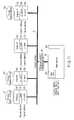
- a MPU 1includes an integrated memory management device 2 , and accesses a NAND type flash main memory 4 .
- the NAND type flash main memory 4stores an address conversion table 5 and rewrite frequency data 6 inside.
- the rewrite frequency data 6corresponds to main memory history data showing an accessed state of the main memory.
- the address conversion table 5is data associating a logical address with a physical location (or physical address) in the NAND type flash main memory 4 .
- the rewrite frequency data 6shows the number of rewrite times of each page or block of the NAND type flash main memory 4 .
- the integrated memory management device 2includes MMU 7 , cache controller 8 , primary cache memory 3 , secondary cache memory 22 , main memory MMU 9 , and access history storage (NAND information registers) 10 .
- the cache controller 8includes a first cache controller 8 a used for the primary cache memory 3 and a second cache controller 8 b used for the secondary cache memory 22 .
- the main memory MMU 9includes an address relation storage 23 . The address relation storage 23 may be separated from the main memory MMU 9 .
- the first embodimentrelates to the case where the cache memory is two.
- the number of cache memoriesmay be one or three or more.
- the MMU 7converts a logical address of the cache memory 3 into a physical address.
- the primary cache memory 3has a tag storage area 3 a and a line storage area 3 b.
- the secondary cache memory 22has a tag storage area 22 a and a line storage area 22 b.
- each line size of the primary and secondary cache memories 3 and 22is set as follows. Specifically, the line size is set to the same size (e.g., 256 kilobytes) as the block of the NAND type flash main memory 4 or to a multiple of the page thereof. In this way, the following operations are carried out at a unit of page, a multiple of the page, or block.
- Oneis an operation of moving data of the NAND type flash main memory 4 to the primary or secondary cache memory 3 or 22 .
- Anotheris an operation of moving data of the primary or secondary cache memory 3 or 22 to the NAND type flash main memory 4 .
- data movecan be simplified.
- the primary and secondary cache memories 3 and 22are a write back type.
- the secondary cache memory 22has a storage capacity larger than the primary cache memory 3 ; however, the operation is low speed.
- the first cache controller 8 acontrols access to the primary cache memory 3 .
- the first cache controller 8 awhen reading data from the primary cache memory 3 , the first cache controller 8 a reads data corresponding to a physical address of the primary cache memory 3 according to the physical address obtained from the MMU 7 .
- the first cache controllerWhen writing data to the primary cache memory 3 , the first cache controller writes write target data to a location corresponding to the physical address of the primary cache memory 3 according to the physical address obtained from the MMU 7 .
- the second cache controller 8 bcontrols access to the secondary cache memory 22 .
- the second cache controller 8 bwhen reading data from the secondary cache memory 22 , the second cache controller 8 b reads data corresponding to a physical address of the secondary cache memory 22 according to the physical address obtained from the MMU 7 .
- the second cache controllerWhen writing data to the secondary cache memory 22 , the second cache controller writes write target data to a location corresponding to the physical address of the secondary cache memory 22 according to the physical address obtained from the MMU 7 .
- the main memory MMU 9controls access to the NAND type flash main memory 4 .
- the main memory MMU 9stores part or all of the address conversion table 5 of the NAND type flash main memory 4 in the address relation storage 23 as address relation data if necessary.
- the main memory MMU 9stores part or all of the rewrite frequency data 6 of the NAND type flash main memory 4 to the access history storage 10 as access history data if necessary.
- the main memory MMU 9converts the logical address of the NAND type flash main memory 4 to a physical location.
- the main memory MMU 9reads data from the NAND type flash main memory 4 based on the physical location of the NAND type flash main memory 4 . Thereafter, the main memory MMU 9 stores the read data in the primary or secondary cache memory 3 or 22 using the first or second cache controller 8 a or 8 b.
- the main memory MMU 9When reading new data from the NAND type flash main memory 4 , the main memory MMU 9 reads address conversion table data and rewrite frequency data related to the new data. Thereafter, the main memory MMU 9 stores the foregoing two data in the address relation storage 23 and the access history storage 10 , respectively.
- the main memory MMU 9executes the following controls based on the foregoing address relation data and access history data.
- Oneis a control of accessing all area or all blocks of the NAND type flash main memory 4 equally (regardless of the kind).
- Anotheris a control for equalizing the rewrite frequency of each area or block of the NAND type flash main memory 4 .
- Anotheris a control of avoiding a defective area or defective block.
- the main memory MMU 9acquires data stored in the primary or secondary cache memory 3 or 22 using the first or second cache controller 8 a or 8 b . Then, the main memory MMU 9 stores the acquired data in the NAND type flash main memory 4 based on the physical location of the NAND type flash main memory 4 .
- the main memory MMU 9updates the address relation data of the address relation storage 23 based on the relationship between a logical address and a physical location related to the written data.
- the main memory MMU 9further updates the access history data of the access history storage 10 .
- the main memory MMU 9reflects the following data to the address conversion table 5 and the rewrite frequency data 6 of the NAND type flash main memory 4 .
- Oneis the address relation data stored in the main memory MMU 9 and another is the access history data stored in the access history storage 10 .
- the main memory MMU 9matches the address relation data stored in the MPU 1 with the address conversion table 5 stored in the NAND type flash main memory 4 .
- the MMU 9further matches the access history data of the access history storage 10 with the rewrite frequency data of the NAND type flash main memory 4 .
- the access history storage 10stores an access state history of the page or block (physical location) of the NAND type flash main memory 4 . According to this embodiment, the access history storage 10 stores rewrite frequency data of part or all pages or blocks in the rewrite frequency data 6 of each block of the NAND type flash main memory 4 .
- the rewrite frequency of each blockis recorded using four bytes.
- Each block sizeis set to 256 kilobytes.
- the storage capacity of the NAND type flash main memory 4is 1 megabyte
- the number of blocks stored in the NAND type flash main memory 4is four.
- the storage capacity required for storing the rewrite frequency of each blockis 16 bytes.
- the storage capacity required for storing the rewrite frequency of each blockis 16 kilobytes.
- the storage capacity of the NAND type flash main memory 4is 16 gigabytes
- the storage capacity required for storing the rewrite frequency of each blockis 64 kilobytes.
- the access history storage 10stores part of the rewrite frequency data 6 in the NAND type flash main memory 4 .
- a symbol “pos”is marked on the rewrite frequency because the access history storage 10 stores part of the rewrite frequency data 6 .
- the “pos”is used the same manner as a cache tag.
- the main memory MMU 9stores part of the address conversion table 5 of the NAND type flash main memory 4 in the address relation storage 23 .
- the main memory MMU 9further stores part of the rewrite frequency data 6 in the access history storage 10 .
- the main memory MMU 9When the cache memories 3 and 22 does not store read target data, the main memory MMU 9 reads the data from there. Thereafter, the main memory MMU 9 stores data which corresponds to the read data and is included in the address conversion table 5 in the address relation storage 23 . In addition, the main memory MMU 9 stores data which corresponds to the read data and is included in the rewrite frequency data 6 in the access history storage 10 .
- the main memory MMU 9converts a logical address of the NAND type flash main memory 4 into a physical location. Then, the main memory MMU 9 writes write target data in cache lines 3 b and 22 b to the NAND type flash main memory 4 . In addition, the main memory MMU 9 updates address relation data stored in the address relation storage 23 and access history data stored in the access history storage 10 .
- the main memory MMU 9updates the address conversion table 5 and the rewrite frequency data 6 based on the address relation data of the address relation storage 23 and the access history data of the access history storage 10 .
- the main memory MMU 9overwrites data read from the NAND type flash main memory 4 on the primary cache memory 3 using the first cache controller 8 a .
- the first cache controller 8 areads data from the first cache memory 3 .
- the MPU 1executes a program to write the obtained data to the cache memory 3 .
- the main memory MMU 9reads the written-back data from the cache memory 3 via the first cache controller 8 a .
- the main memory MMU 9selects a page or block having rewrite frequency less than a predetermined number as a write back location of the NAND type flash main memory 4 based on the access history data of the access history storage 10 . Thereafter, the main memory MMU 9 stores the written-back data in the selected page or block.
- the main memory MMU 9updates address relation data showing a conversion relationship between a logical address and a physical location in the NAND type flash main memory 4 with respect to the selected page or block.
- the main memory MMU 9further updates the rewrite frequency of the access history storage 10 with respect to the selected page or block.
- the main memory MMU 9updates the address conversion table 5 and the rewrite frequency data 6 according to the contents of the address relation storage 23 and the access history storage 10 .
- FIG. 2is a view showing one example of a memory hierarchy of the integrated memory management device 2 of this embodiment.
- the memory hierarchyhas a hierarchy belonging to the MMU 7 , and a hierarchy belonging to the main memory MMU 9 and the cache controller 8 .
- a logical addressis converted into a physical address.
- access destinationthat is, the physical location of the NAND type flash main memory 4 is determined.
- access control for a page or block having rewrite frequency less than a predetermined numberis carried out.
- the integrated memory management device 2accesses the NAND type flash main memory 4 based on the determined physical location.
- FIG. 3is a flowchart to explain an example of an operation when the MPU 1 including the integrated memory management device 2 stores data of the NAND type flash main memory 4 , part of the rewrite frequency data 6 of the NAND type flash main memory 4 , and part of the address conversion table 5 of the NAND type flash main memory 4 in the MPU 1 .
- step S 1the main memory MMU 9 reads partial data (first, 1 gigabyte from the header) of the NAND type flash main memory 4 used by the MPU 1 .
- the cache controller 8writes the read data to cache lines 3 b and 22 b of the cache memories 3 and 22 .
- step S 2the main memory MMU 9 copies part of the rewrite frequency data 6 stored in the NAND type flash main memory 4 into the access history storage 10 included in the MPU 1 . (i.e., the part is rewrite frequency of the block with respect to data stored in cache memories 3 and 22 . Incidentally, data equivalent to 1 gigabyte from the header may be first copied.)
- step S 3the main memory MMU 9 copies part of the address conversion table 5 stored in the NAND type flash main memory 4 into the address relation storage 23 of the main memory MMU 9 of the MPU 1 .
- the partis data showing the relationship between logical address and physical location of the block corresponding to data stored in cache memories 3 and 22 .
- data equivalent to 1 gigabyte from the headermay be first copied.
- FIG. 4is a flowchart to explain an example of an operation of reading data from the primary cache memory 3 or NAND type flash main memory 4 by the MPU 1 including the integrated memory management device 2 .
- the case of reading data from the secondary cache memory 22is the same as the case of the primary cache memory 3 .
- step T 1the MMU 7 and the main memory MMU 9 converts a read target logical address to a physical address.
- step T 2 athe first cache controller 8 a reads the read target data from the primary cache memory 3 based on the physical address.
- step T 2 bthe main memory MMU 9 reads data corresponding to the physical address from the NAND type flash main memory 4 .
- step T 3 bthe main memory MMU 9 overwrites the data read from the NAND type flash main memory 4 onto the primary cache memory 3 via the first cache controller 8 a.
- the main memory MMU 9stores data corresponding to the newly read data in the address relation storage and the access history storage based on the address conversion table 5 and the rewrite frequency data 6 of the NAND type flash main memory 4 .
- FIG. 5is a flowchart to explain an example of an operation when overwrite to the cache line 3 b of the primary cache memory 3 is generated from the MPU 1 including the integrated memory management device 2 of this embodiment and data in the Primary cache memory 3 is stored in the NAND type flash memory 4 .
- the case where overwrite to the secondary cache memory 22 is generatedis the same as the case of the primary cache memory 3 .
- step U 1the MMU 7 makes conversion from logical address to physical address.
- step U 2the first cache controller 8 a stores write target data in the primary cache memory 3 in accordance with the physical address.
- step U 3the main memory MMU 9 selects a location of a block having rewrite frequency less than a predetermined value or a location of a block having the least rewrite frequency as a rewrite location of the NAND type flash main memory 4 based on the following data.
- Oneis address relation data of the address relation storage 23
- anotheris access history data of the access history storage 10 .
- step U 4the main memory MMU 9 stores the write target data in the selected location of the NAND type flash main memory 4 .
- step U 5the main memory MMU 9 updates the address relation data of the address relation storage 23 so that the data corresponds to the cache line 3 b after overwritten.
- the main memory MMU 9further updates the access history data of the access history storage 10 .
- step U 6the main memory MMU 9 updates the address conversion table 5 of the NAND type flash main memory 4 to match with the address relation data stored in the main memory MMU 9 .
- the main memory MMU 9updates the rewrite frequency data 6 of the NAND type flash main memory 4 to match with the address history data stored in the access history storage 10 .
- update of rewrite frequency data 6 of the NAND type flash main memory 4is executed when the power of the MPU 1 is turned off or when the access history storage 10 of the MPU 1 is rewritten.
- the integrated memory management device 2selects a physical location of the rewritten block based on rewrite frequency. Moreover, the integrated memory management device 2 executes the following controls in place of the foregoing control (operation). One is control of avoiding a defective area or block, and another is control of accessing all areas or blocks of the NAND type flash main memory 4 equally. Another is control of dispersing a location of the access destination area or block. In this case, the access history storage 10 is stored with data such as a generating location of a defective area or block stored in the NAND type flash main memory 4 or rewrite location distribution thereof. The integrated memory management device 2 may freely combine various controls to select a location of the rewritten area or block.
- the integrated memory management device 2may execute garbage collection or erase control in the NAND type flash main memory 4 when interchanging data of cache memory 3 .
- data of at least one of the address relation storage 23 and the access history storage 10 of the main memory MMU 9may be stored in the secondary cache memory 22 .
- the address relation data stored in the address relation storage 23may be stored in the secondary cache memory 22 .
- access history data including rewrite frequency stored in the access history storage 10may be stored in the secondary cache memory 22 .
- the integrated memory management device 2 of the MPU 1employs the following algorithm.
- the write targetthat is, a physical location of the NAND type flash main memory 4 is selected using data stored in the access history storage 10 , and then, written back.
- the integrated memory management device 2can utilize a program for executing the foregoing algorithm. For example, it is possible to employ excellent algorithm of avoiding rewriting a block having many rewrite frequencies.
- the foregoing integrated memory management device 2employs the following configuration in the MPU 1 .
- the foregoing MMU 7 , first and second cache controllers 8 a , 8 b , cache memories 3 , 22 , main memory MMU 9 and access history storage 10are integrated.
- the following architectureis realized. Namely, memory mapping management of the NAND type flash main memory 4 is executed by the integrated memory management device 2 of the MPU 1 .
- the MPU 1executes an operation of a memory controller included in a general NAND type flash memory. As described above, the operation of the MPU and the operation of the memory controller are combined, and then, executed by the MPU 1 , and thereby, memory control are cooperated.
- the memory hierarchyis simple; therefore, a programmer easily grasps a hierarchy where MMU conversion and a generation of replacement of the cache memory are made. Thus, this serves to easily carry out program optimization.
- the second embodimentrelates to a modification example of the foregoing first embodiment.
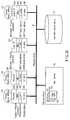
- FIG. 6is a bloc diagram showing an example of an integrated memory management device according to the second embodiment.
- a MPU 11includes an integrated memory management device 12 according to the second embodiment.
- An integrated MMU 13realizes a function of integrating the MMU 7 and the main memory MMU 9 of the first embodiment.
- each tag of the primary and secondary cache memories 3 and 22is used for managing these cache memories 3 and 22 using a process ID and a logical address.
- the integrated MMU 13 of a processorthat is, MPU 11 executes a memory mapping management of primary and secondary cache memories 3 , 22 and the NAND type flash main memory 4 .
- various memoriesare integrally managed.
- FIG. 7is a view showing an example of a memory hierarchy of the integrated memory management device 12 according to the second embodiment.
- the integrated memory management device 12integrates address conversions for the primary and secondary cache memories 3 , 22 , and an address conversion for the NAND type flash main memory 4 .
- the address conversionsbelong to the same memory layer.
- the integrated memory management device 12decides an access target area of the primary and secondary cache memories 3 , 22 and the NAND type flash main memory 4 .
- the memory hierarchybelongs to the same hierarchy as the integrated MMU 13 and the cache controller 8 .
- the integrated memory management device 12accesses the NAND type flash main memory 4 based on the determined physical location.
- the MMU 7 and the main memory MMU 9 of the first embodimentare integrated. By doing so, the configuration is simplified, and it is possible to reduce various costs such as time cost required for access and economic cost required for manufacture.
- the integrated MMU 13is used, and thereby, the following address conversions are integrated.
- Oneis an address conversion with respect to the primary and secondary cache memories 3 and 22 .
- Anotheris an address conversion with respect to the NAND type flash main memory 4 .
- storage contents related to a certain processis stored in a near location in the NAND type flash main memory 4 as much as possible. This serves to enable high-speed access. For example, only block having few rewrite frequency is selected, and then, assigned to one process.
- the third embodimentrelates to modification examples of the integrated memory management devices 2 and 12 according to the foregoing first and second embodiments.
- FIG. 8is a block diagram showing an example of an integrated memory management device 2 according to a modification example of the first embodiment.
- the main memory MMU 9accesses the NAND type flash main memory 4 based on the physical address.
- the cache controller 8may execute access to the NAND type flash main memory 4 based on the physical address.
- the main memory MMU 9executes control of converting a logical address to a physical location. Then, the cache controller 8 accesses the NAND type flash main memory 4 based on the physical location selected by the main memory MMU 9 . According to this embodiment, the cache controller 8 reads and updates the address conversion table 5 and the rewrite frequency data 6 of the NAND type flash main memory 4 in place of the main memory MMU 9 .
- FIG. 9is a block diagram showing an example of an integrated memory management device 12 according to a modification example of the first embodiment.
- the integrated MMU 13executes access to the NAND type flash main memory 4 based on the physical location.
- the cache controller 8may execute access to the NAND type flash main memory 4 based on the physical address.
- the integrated MMU 13executes control of converting a logical address to a physical location. Then, the cache controller 8 accesses the NAND type flash main memory 4 based on the physical location selected by the integrated MMU 13 . According to this embodiment, the cache controller 8 reads and updates the address conversion table 5 and the rewrite frequency data 6 of the NAND type flash main memory 4 .
- the fourth embodimentrelates to an example to which the integrated memory management devices 2 and 12 according to the foregoing first to third embodiments are applied.
- FIG. 10is a block diagram showing an applied example of an integrated memory management device according to the fourth embodiment.
- the fourth embodimentmakes an explanation about the case where an integrated memory management device 20 is applied to a game machine.
- the integrated memory management device 20is applied to other devices such as car navigation system in the same manner.
- the integrated memory management devices 2 , 12 of the foregoing first embodimentmay be used in place of the integrated memory management device 20 .
- a portable game console processor 14includes a graphics processor 15 and a processor 16 .
- the graphics processor 15 , the processor 16 , a secondary cache memory 17 , a NAND type flash main memory 4 and a disk drive 18are connected to a bus 19 .
- the processor 16includes a primary cache memory 3 , a secondary cache tag 21 for accessing the secondary cache memory 17 , a cache controller 8 and an integrated MMU 13 .
- the processor 16further includes a rewrite frequency storage 10 ; however, the rewrite frequency storage 10 is not illustrated in FIG. 10 .
- the processor 16may use the primary or secondary cache memory 3 or 17 as the rewrite frequency storage 10 .
- the cache controller 8controls access to the primary and secondary cache memories 3 and 17 .
- a DRAMis usable as the secondary cache memory 17 .
- the secondary cache memory 17is separated from the portable game console processor 14 .
- a band width to the secondary cache memory 17is set to about ten times as much as the NAND type flash main memory 4 .
- an optical disk driveis usable as the disk drive 18 .
- write to the NAND type flash main memory 4is executed when a game cartridge is replaced.
- the NAND type flash main memory 4is used in read only. Frequently written data or program code and frequently read data or program code are stored in the secondary cache memory 17 . In addition, the frequently read data or program code is stored in the primary cache memory 3 .
- data or program code having low frequencyis written to the NAND type flash main memory 4 .
- data or program code having high frequencymay be stored in the primary or secondary cache memory 3 or 17 .
- the primary cache memory 3has a data capacity of about 64 kilobytes
- the secondary cache memory 17has a data capacity of about 16 to 128 megabytes
- the NAND type flash main memory 4has a data capacity of about 1 gigabytes.
- the graphics processor 15has processing capabilities balanced with a speed of the NAND type flash main memory 4 having 1/10 band width or about two or three times as much as the speed. Low frequency data is read from the NAND type flash main memory 4 ; conversely, high frequency data is read from the primary or secondary cache memory 3 or 17 .
- garbage collection and erase of the NAND type flash main memory 4are carried out when cache is replaced (cache miss).
- cache missit is possible to provide a processor 16 , which can realize optimization described above. Thus, preferable optimization is effected.
- An entry size of the secondary cache memory 17is set to about 1 megabyte, and thereby, the secondary cache memory 17 has good compatibility with the NAND type flash main memory 4 .
- the processor 16is provided with the integrated MMU 13 , and thereby, the primary cache memory 3 , the secondary cache memory 17 and the NAND type flash main memory 4 are integrally managed.
- data or programis stored in the NAND type flash main memory 4 , and thereby, access to the disk drive 18 is reduced.
- thisserves to reduce wait time, and to improve user's operability and satisfaction.
- the NAND type flash main memory 4having a memory unit price cheaper than the secondary cache memory 17 (DRAM) is used, and thereby, a large number of data or program is accessible at high speed.
- DRAMsecondary cache memory 17
- the fifth embodimentrelates to an integrated memory management device which is interposed between a plurality of processors and a main memory.
- FIG. 11is a block diagram showing the configuration of an integrated memory management device according to a fifth embodiment.
- the memory device of this embodimentincludes an integrated memory management device 24 .
- the integrated memory management device 24is connected with a plurality of processors (for example, Codec IP or Graphic IP) 251 to 254 via a system bus 30 .
- the integrated memory management device 24is applied to the multiprocessor configuration.
- the integrated memory management device 24is further connected with a non-volatile main memory 26 such as a NAND type flash memory, for example.
- the number of processorsis one or more, and may be freely changeable.
- writing and readingare carried out at a unit of plural bits called as a page. Erasing is collectively carried out at a unit collecting a plurality of pages called as a block.
- processors 251 to 254execute a process including a logical address.
- processors 251 , 252 and 254execute processes 271 , 272 and 274 , respectively.
- the foregoing processes 271 , 272 and 274may be an operating system.
- the processors 251 to 254include primary cache memories 281 to 284 and secondary cache memories 291 to 294 , respectively.
- the integrated memory management device 24executes wear leveling, and makes a conversion from a logical address to a physical address.
- the integrated memory management device 24executes wear leveling at a page unit, a multiple unit of the page or block unit of the main memory 26 .
- a wear leveling counteris stored in a redundancy area 26 a of the main memory.
- the redundancy area 26 ais a redundancy area given every page or block of the main memory 26 .
- the integrated memory management device 24handles a removable memory as a main memory, and maps it in a memory space.
- the integrated memory management device 24is provided on the side of the main memory 26 rather than the side of the processors 271 to 274 . However, the integrated memory management device 24 may be provided on the side of the processors 271 to 274 .
- the integrated memory management device 24changes a page size based on an instruction and data. For example, an instruction page size is set to a small size such as 16 kilobytes, and a data page size is set to a large size such as 512 kilobytes.
- the main memory 26has the same memory page size as the page size (process or OS) of the integrated memory management device 24 or a memory page size of multiple of the page size of the MMU.
- Page transmissionis collectively executed between primary and secondary cache memories 281 to 284 and 291 to 294 and the main memory 26 .
- the batch transmissionis carried out at the page unit, the multiple unit of the page or the block unit of the main memory (e.g., 256 kilobytes to 512 kilobytes).
- Access to primary and secondary cache memories 281 to 284 and 291 to 294is made based on a logical address.
- the logical addressis used on the system bus 30 .
- the integrated memory management device 24integrally executes the following conversions.
- Oneis a conversion from a process level logical address to a physical address with respect to the processors 271 to 274 .
- Anotheris a conversion from a logical page or logical block to a physical block for the wear leveling of the page unit, the multiple unit of the page or block unit of the main memory 26 .
- a system logical address 31 having a format shown in FIG. 12is used.
- the system logical address 31is composed of a processor ID and a process ID and a process internal logical address. At least one of processor ID and a process ID is may be converted. For example, the length of at least one of the processor ID and process ID is may be shortened by hashing. And the system logical address 31 may include a converted content. For example, the processor ID and process ID may be converted by hashing, and the system logical address 31 may include converted bits by hashing and the process internal logical address.
- the main memory 26is stored with a page table 26 b in the entire system. Specifically, the main memory 26 has a page table 26 b integrating processes 271 , 272 and 274 , and does not have a page table every process 271 , 272 and 274 .
- a main memory having the same capacity as HDDis used as the main memory 26 .
- the physical memoryis a DRAM, and has a capacity of about 1 GB.
- a secondary storage areais secured on the HDD having a larger storage capacity, and then, swap in/swap out must be executed.
- the main memoryhas the same level storage as the HDD capacity; therefore, the secondary storage does not need to be used.
- the sixth embodimentrelates to a modification example of the foregoing fifth embodiment.
- FIG. 13is a block diagram showing the configuration of an integrated memory management device according to a sixth embodiment.
- a plurality of integrated memory management devices 241 and 242is connected with a plurality of processors (including Codec IP, graphic IP) 251 to 254 via a network.
- the integrated memory management devices 241 and 242are connected with a plurality of non-volatile main memories 261 and 262 such as NAND type flash memory, for example.
- the number of the MMUs and the number of the main memoriesmay be freely changeable.
- the main memory 261has the same features as the main memory 26 of the foregoing fifth embodiment.
- the main memory 261has a redundancy area 261 a , which stores a wear leveling counter, and a page table 261 b , which integrates these processes 271 , 272 and 274 .
- the main memory 262has the same features as the main memory 261 .
- a logical address 34is used.
- the logical address shown in FIG. 14is composed of IP address or IPv6 address of the network 33 , processor ID and process ID, and process internal logical address. At least one of address and ID is may be converted. For example, the length of at least one of the address and ID is may be shortened by hashing. And the logical address 34 may include a converted content. For example, IP address or IPv6 address, the processor ID and process ID may be converted by hashing, and the logical address 34 may include converted bits by hashing and the process internal logical address.
- the main memories 261 and 262have the same memory page size as that of the integrated memory management devices 241 and 242 or has a memory page size of integer multiples of the page size of the integrated memory management devices 241 and 242 .
- Page transmissionis collectively executed between primary cache memories 281 to 284 and secondary cache memories 291 to 294 and main memories 261 and 262 .
- the batch transmissionis executed at a page unit, integer multiples unit of the page size, or block unit (e.g., 256 kilobytes to 512 kilobytes) of the main memory.
- access to the primary cache memories 281 to 284 and to secondary cache memories 291 to 294is made based on a logical address.
- a logical addressis used on the network 33 .
- the integrated memory management devices 241 and 242integrally make the following conversions.
- Oneis a conversion from a process level logical address to a physical address with respect to the processors 271 to 274 .
- Anotheris a conversion from a logical page or block to a physical page or block for wear leveling of the page unit, integer multiples unit of the page size, or block unit of the non-volatile main memories 261 and 262 .
- the same effect as the foregoing fifth embodimentis obtained in a wide memory space via the network 33 .
- the seventh embodimentrelates to a modification example of the foregoing fifth and sixth embodiments.
- a modification example of the fifth embodimentwill be hereinafter described.
- the sixth embodimentmay be also modified in the same manner.
- FIG. 15is a block diagram showing the configuration of an integrated memory management device according to a seventh embodiment.
- a plurality of processors 351 to 354is connected with a main memory 26 via a system bus 30 . According to this embodiment, the number of processors may be freely changeable.
- processors 351 to 354execute a process including a logical address.
- processors 351 , 352 and 354execute processes 271 , 272 and 274 , respectively.
- the foregoing processes 271 , 272 and 274may be an operating system.
- the foregoing processors 351 to 354include primary cache memories 361 to 364 , secondary cache memories 371 to 374 and MMUs 381 to 384 , respectively.
- the MMUs 381 to 384each execute wear leveling, and make a conversion from a logical address to a physical address. These MMUs 381 to 384 are provided on the side of the processors 351 to 354 .
- the main memory 26has the same memory page size as that of the MMUs 381 to 384 or has a memory page size of integer multiples of the page size of the MMUs 381 to 384 .
- Page transmissionis collectively executed between primary cache memories 361 to 364 and secondary cache memories 371 to 374 and the main memory 26 .
- the batch transmissionis executed at a block (page) unit (e.g., 256 kilobytes to 512 kilobytes) of the main memory.
- a physical addressis used for making access to primary cache memories 361 to 364 and for making access to secondary cache memories 371 to 374 .
- a physical addressis also used on the system bus 30 .
- the MMUs 381 to 384 provided for the processors 351 to 354each make the following conversions.
- Oneis a conversion from a process level logical address to a physical address.
- Anotheris a conversion from a logical address to a physical address for wear leveling of a page unit, integer multiples unit of the page size, or block unit of the main memory 26 .
- the seventh embodimenteven if the MMUs 381 to 384 are provided on the side of the processors 351 to 354 , the same effect as the foregoing fifth embodiment is obtained.
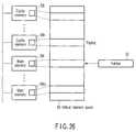
- FIG. 16is a block diagram illustrating an example of the structure of an integrated memory management device 24 according to this embodiment.
- a NAND type flash main memory 26includes a physical block 39 corresponding to a physical address, a page table 26 b , memory usage information 40 , and memory peculiarity (unique) information 41 .
- the cache line size of each of the primary cache memories 281 to 284 and the secondary cache memories 291 to 294 of the processors 251 to 254is equal to the integral multiples of the page size or the block size of the NAND type flash main memory 26 , which makes it possible to improve the transmission efficiency of data.
- various types of datasuch as data D 1
- data D 1may exist in a plurality of physical blocks 39 .
- a plurality of data, such as data D 1 and D 2may exist in one physical block 39 .
- the data D 1 and D 2may include unique read/write (read and write) frequency information items E 1 and E 2 , respectively.
- each of the data D 1 and D 2includes at least one of static information and dynamic information.
- the static informationmeans a predetermined value.
- the dynamic informationincludes the number of times data is actually rewritten and the number of times data is actually read.
- information indicating that data for a captured image is read or written one time for two hours immediately after image capture, and information indicating that data for a captured image is read one time within two weeks and is not written after three days have elapsed from image captureis stored as the static information of image data of a digital camera.
- the following informationis stored as the static information of the cache information of a web browser: information indicating that data is written and read one time for several minutes; information indicating that the information of a site, which is accessed a predetermined number of times or more, is written one time per day; information indicating that, when there is a periodic access pattern, the information thereof is written according to the periodic access pattern; and information indicating that the number of write operations is large for a predetermined amount of time.
- the static informationneeds to include a value that is effective for various types of data.
- a static information setting filemay be shared on a network.
- One page table 26 bmay suffice for one system. Alternatively, the page table 26 b may not be provided.
- the memory usage information 40includes the number of read and write operations in each memory area and the number of times each data is read and written. Specifically, for example, the memory usage information 40 includes the number of times data is rewritten in each memory area (page or block), the number of times data is read from each memory area, and data information (for example, the number and type of data information items, the number of times data is read, and the number of times data is rewritten) stored in the memory area.
- the memory peculiarity information 41includes, for example, the page size and the block size of the NAND type flash main memory 26 , the number of times data can be rewritten in the memory, and the number of time data can be read from the memory.
- the memory peculiarity information 41includes the page size and the block size of the NAND type flash main memory 26 , the total storage capacity of the memory, SLC (single level cell) area information (for example, a block position, a size, the number of times data can be read, and the number of times data can be written), and MLC (multi level cell) area information (for example, a block position, a size, the number of times data can be read, and the number of times data can be written).
- the integrated memory management device 24converts a logical address for each process (or an OS) into a physical address, and converts a logical address for the NAND type flash main memory 26 into a physical address.
- the integrated memory management device 24performs optimal wear-leveling on the basis of the read/write frequency information items E 1 and E 2 peculiar to the data D 1 and D 2 , the memory usage information 40 , and the memory peculiarity information 41 .
- the integrated memory management device 24includes a microprocessor 42 , a work memory 43 , an information register 44 , and a cache memory 45 .
- the microprocessor 42uses the information register 44 and the work memory 43 to perform memory management.
- the cache memory 45temporarily stores data from the processors 271 to 274 and data from the NAND type flash main memory 26 .
- the cache memory 45may be an external DRAM.
- FIG. 17is a block diagram illustrating an example of the function of the microprocessor 42 .
- the microprocessor 42has an acquisition function 42 a , an address conversion function 42 b , an access function 42 c , and a transmission function 42 d.
- the acquisition function 42 aacquires a read logical address from any one of the plurality of processors 251 to 254 .
- the address conversion function 42 bconverts the read destination logical address acquired by the acquisition function 42 a into the read destination physical address of the NAND type flash main memory 26 .
- the NAND type flash main memory 26is divided into areas having each group attribute.
- the NAND type flash main memory 26comprises memory peculiarity information 41 including the group attributes of the areas.
- the address conversion function 42 brefers to read/write frequency information items E 1 and E 2 peculiar to data D 1 and D 2 and the memory peculiarity information 41 .
- the read/write frequency information items E 1 and E 2are defined by an operating of a file management program (process) on a processor.
- the address conversion function 42 bdecides the write destination physical address representing an area corresponding to the group attribute of the read/write frequency information items E 1 and E 2 peculiar to data D 1 and D 2 .
- the access function 42 creads data corresponding to the read destination physical address from the NAND type flash main memory 26 .
- the size of the read datais equal to a page size, the integer multiples of the page size of the NAND type flash main memory 26 , or the block size thereof.
- the transmission function 42 dtransmits the read data to the cache memory of the processor that has issued the read logical address.
- the cache size of the cache memory of the processor that has issued the read logical addressdepends on (e.g., equal to) a page size, the integer multiples of the page size of the NAND type flash main memory 26 , or the block size thereof.
- the acquisition function 42 aacquires a write destination logical address and write data from the processor.
- the size of the write datais equal to the cache size.
- the address conversion function 42 bconverts the write destination logical address acquired by the acquisition function 42 a into the write destination physical address of the NAND type flash main memory 26 .
- the access function 42 cwrites the write data in the NAND type flash main memory 26 at a position corresponding to the write destination physical address.
- the address conversion function 42 b of the microprocessor 42performs wear-leveling on the basis of at least one of the read/write frequency information items peculiar to data, the memory usage information 40 , and the memory peculiarity information 41 .
- FIG. 18is a diagram illustrating an example of the first operation of a transmission algorithm of the integrated memory management device 24 .
- the microprocessor 42 of the integrated memory management device 24reads out the memory usage information 40 and the memory peculiarity information 41 and stores the information in the information register 44 during start-up.
- the memory peculiarity information 41includes the page size and the block size of the NAND type flash main memory 26 .
- the cache size of each of the processors 271 to 274is equal to a page size, the integer multiples of the page size of the NAND type flash main memory 26 or the block size thereof.
- the microprocessor 42When the integrated memory management device 24 is applied to the existing processor and it is impossible to change the cache size of the processor, the microprocessor 42 performs buffering in the cache memory 45 to adjust a difference between the cache size of each of the processor 271 to 274 and the integer multiple of the page size or the block size of the NAND type flash main memory 26 . For example, the microprocessor 42 reads data corresponding to a 256-kilobyte page size to the cache memory 45 , and outputs data corresponding to a cache line of 4 kilobytes to any one of the processors 271 to 274 .
- FIG. 19is a diagram illustrating an example of the second operation of the transmission algorithm of the integrated memory management device 24 .
- the microprocessor 42 of the integrated memory management device 24receives an access request corresponding to one cache line from the processor 252 (Tr 19 A).
- the microprocessor 42reads data that is equal to a block or the integer multiple of a page corresponding to the access request from the NAND type flash main memory 26 , and stores the read data in the cache memory 45 (Tr 19 B).
- the microprocessor 42transmits data corresponding to the access request from the cache memory 45 to the processor 252 (Tr 19 C).
- FIG. 20is a diagram illustrating an example of the third operation of the transmission algorithm of the integrated memory management device 24 .
- the processor 252rewrites data in the cache memory 282 or the cache memory 292 (Tr 20 A).
- the microprocessor 42 of the integrated memory management device 24caches out the data written in the cache memory 282 or the cache memory 292 , and transmits the data to the cache memory 45 (Tr 20 B).
- the microprocessor 42performs wear-leveling on the basis of the read/write frequency information items included in the data, and the memory usage information 40 and the memory peculiarity information 41 stored in the information register 44 to determine a physical block 39 for data writing among a plurality of physical blocks of the NAND type flash main memory 26 .
- the microprocessor 42stores the rewritten data stored in the cache memory 45 in the determined physical block 39 (Tr 20 C).
- FIG. 21is a block diagram illustrating an example of the wear-leveling.
- the NAND type flash main memory 26includes two or more banks 46 a and 46 b.
- the microprocessor 42additionally stores data (a block or a page) in one bank 46 a.
- the microprocessor 42When data is erased, the microprocessor 42 erases target data from the bank 46 a . However, until data is stored in the last area of the bank 46 a , the additional data storage process is sequentially performed. In the bank 46 a , which is a write target, data writing is not performed on an area from which data is erased. Therefore, when data is erased from the bank 46 a , which is a write target, the area from which the data is erased is empty.
- the microprocessor 42copies valid data that has not been erased from the bank 46 a to the bank 46 b while performing garbage collection, and additionally stores new data in the bank 46 b , starting from the area following the area in which the copied data is stored.
- the microprocessor 42copies data of a bank to another bank, and then clears the bank. Then, the same process as described above is repeated.
- the microprocessor 42receives data to be written from a processor or an OS. When there is a plurality of data to be written, data having the highest write frequency is used as a standard. When the existing processor or OS is used, the microprocessor 42 examines the head of data to determine the type of data.
- the microprocessor 42determines an MLC area as a rewrite area.
- the microprocessor 42determines an empty area in which the rewrite frequency is high as a rewrite area.
- the microprocessor 42determines an SLC area as the rewrite area.
- the microprocessor 42determines an empty block having the lowest rewrite frequency in the SLC area or the MLC area as a write area.
- the microprocessor 42selects an area having a low rewrite frequency on the basis of static information and an area having a low rewrite frequency on the basis of dynamic information, from the areas in which data has already been written. Then, the microprocessor stores, in an empty area, the data in the selected area. Then, the microprocessor 42 erases the data stored in the selected area. That is, the microprocessor shifts data from the selected area to an empty area.
- the microprocessor 42 of the integrated memory management device 24may manage a plurality of NAND type flash main memories 26 .
- FIG. 22is a perspective view illustrating an example of the integrated memory management device 24 that manages a plurality of NAND type flash main memories 26 .
- One integrated memory management device 24 and a plurality of NAND type flash main memories 26form one memory unit 47 .
- three memory units 47are formed.
- the integrated memory management device 24manages an access to a plurality of NAND type flash main memories 26 belonging to one memory unit 47 .
- a plurality of integrated memory management devices 24 provided in the plurality of memory units 47are operated such as one memory management device in cooperation with each other.
- the integrated memory management device 24 of the memory unit 47includes an ECC function and an RAID function for a plurality of NAND type flash main memories 26 in the memory unit 47 , and performs mirroring and striping.
- Each of the NAND type flash main memories 26is hot-swappable (replaceable) even when the memory unit 47 is turned on (operated).
- Each of the plurality of NAND type flash main memories 26is provided with a button 48 .
- the button 48includes an alarm output unit (for example, an LED).
- the alarm output unithas a first color (green) indicating a normal condition and a second color (red) indicating that replacement is needed.
- the button 48When the button 48 is pushed, a notification signal is transmitted to a process and an OS. In a stable state in which access is not performed, the button 48 has a third color (blue), and the NAND type flash main memory 26 corresponding to the button 48 is hot-swappable.
- the microprocessor 42 of the integrated memory management device 24determines whether the number of rewrite operations or read operations of each of the NAND type flash main memories 26 reaches the upper limit described in the memory peculiarity information 41 on the basis of the memory usage information 40 and the memory peculiarity information 41 stored in the information register 44 . Then, when it is determined that the number of rewrite operations or read operations reaches the upper limit, the microprocessor 42 notifies or alerts that the memory should be replaced.
- the microprocessor 42 of the integrated memory management device 24preloads data, which is more likely to be frequently accessed, to the cache memory 45 in advance, with reference to the data peculiarity (unique) information items E 1 and E 2 of the NAND type flash main memory 26 .
- the microprocessor 42preloads data that has periodicity and is more likely to be accessed within a predetermined period of time before the predetermined period of time elapses.
- FIG. 23is a block diagram illustrating an example of a multi-processor system using the integrated memory management device 24 according to this embodiment, which is compared to the existing processor including an MMU.
- a processor 255is the existing processor, and includes an MMU 495 , a primary cache memory 285 , and a secondary cache memory 295 .
- the processor 255executes a process 275 .
- the system shown in FIG. 23includes both address conversion (translation) by the MMU 495 according to the related art and address conversion by the memory management device according to this embodiment.
- the MMU 495 of the processor 255accesses the NAND type flash main memory 26 , first, it accesses the page table 26 b of the NAND type flash main memory 26 .
- the page table 26 bincludes a content which does not perform address conversion, but passes through the conversion. For example, both an address before conversion and a converted address which are same values in the page table 26 b . Therefore, the MMU 495 of the processor 255 does not perform address conversion, but the integrated memory management device 24 can perform address conversion.
- FIG. 24is a block diagram illustrating an example of a general multi-processor system according to the related art.
- the existing processors 255 to 258 , a main memory 50 , and a secondary storage device 51are connected to a system bus 30 .
- the processors 255 to 258include MMUs 495 to 498 and the primary cache memories 285 to 288 , and the secondary cache memories 295 to 298 , respectively.
- the processors 255 to 258perform the processes 275 to 277 , respectively.
- Each of the MMUs 495 to 498performs translation between a logical address and a physical address. An access from each of the processors 255 to 258 to any one of the primary cache memories 285 to 288 , the secondary cache memories 295 to 298 , the main memory 50 , and the secondary storage device 51 is performed on the basis of the physical address.
- the main memory 50includes page tables 525 to 528 for the processes 275 to 277 .
- a hard disk drivefor example, a hard disk drive, an SSD (solid state drive), or a NAND type flash memory is used as the secondary storage device 51 .
- an SSDsolid state drive
- a NAND type flash memoryis used as the secondary storage device 51 .
- a DRAMis used as the main memory.
- the NAND type flash main memory 26is used as the main memory.
- the bit cost of the DRAMis higher than that of the NAND type flash main memory 26 . Therefore, this embodiment can reduce costs.
- the main memoryis volatile.
- a non-volatile NAND type flash main memory 26is used as the main memory. Therefore, this embodiment can perform instant boot-up, and reduce the time required to load, for example, a program or data to the main memory. As a result, it is possible to increase an operating speed.
- the multi-processor system according to the related artis provided with both the volatile main memory 50 and the non-volatile secondary storage device 51 .
- the multi-processor system according to this embodimentis provided with the NAND type flash main memory 26 . Therefore, it is possible to use a non-volatile main memory and remove the secondary storage device, such as a hard disk.
- the page tables 525 to 528should be shared, which causes access congestion.
- a DRAM or SSDis used for the secondary storage device.
- a disk search timeis not required, and it is possible to reduce the start-up time.
- since a non-volatile main memory is usedit is not necessary to consider the life span of a batter for a main memory when the system is in a sleep state.
- This embodimentcan easily adapt to a multi-processor environment. In this embodiment, times of installation are reduced, and it is possible to remove process migration.
- the integrated memory management device 24performs optimal wear-leveling on the basis of the read/write frequency information items E 1 and E 2 peculiar to data, the memory usage information 40 , and the memory peculiarity information 41 .
- the wear-levelingis performed on the basis of the read/write frequency information items E 1 and E 2 peculiar to data, which makes it possible to perform wear-leveling more efficiently than SSD.
- the integrated memory management device 24reads out the memory peculiarity information 41 from the NAND type flash main memory 26 , and performs a process corresponding to the page size or block size indicated by the memory peculiarity information 41 . In this way, it is possible to use various generations of NAND type flash memories as the NAND type flash main memory 26 .
- the integrated memory management device 24can read out the memory peculiarity information 41 including a page size or a block size from the NAND type flash main memory 26 , and match the page size or block size of the NAND type flash main memory 26 with the cache line size of each processor.
- the integrated memory management device 24manages the life span of the NAND type flash main memory 26 , and gives an alarm. In this way, it is possible to prevent the occurrence of defects.
- the integrated memory management device 24has an RAID function for a plurality of NAND type flash main memories 26 . Therefore, it is possible to hot-swap the NAND type flash main memory 26 to be replaced. In this way, it is possible to easily replace an exhausted NAND type flash main memory 26 .
- FIG. 25is a block diagram illustrating an example of a process of obtaining a pointer for a large address space.
- a pointer 53includes a pointer 53 a for a small address space and a pointer 53 b for a small address space.
- a segment table 54is provided for each process ID 55 , and includes a pointer 56 for a large address space.
- a pointer 57 for a large address spaceis obtained by combining the pointer 53 b for a small address space with the pointer 56 for a large address space on the segment table 54 that is specified by the pointer 53 a for a small address space.
- FIG. 26is a block diagram illustrating an example of the virtual memory space formed between a plurality of cache memories and a plurality of NAND type flash main memories.
- the pointer 57 for a large address spaceindicates any portion of a virtual memory space 60 formed by cache memories 581 to 58 n of a processor and a plurality of NAND type flash main memories 591 to 59 m.
- non-volatile memories other than the NAND type flash memorymay be used as the main memory.
- the integrated memory management devices of the above-described embodimentscan use for both a write back type cache and write through type cache.
Landscapes
- Engineering & Computer Science (AREA)
- Theoretical Computer Science (AREA)
- Physics & Mathematics (AREA)
- General Engineering & Computer Science (AREA)
- General Physics & Mathematics (AREA)
- Memory System Of A Hierarchy Structure (AREA)
- Memory System (AREA)
Abstract
Description
Claims (6)
Priority Applications (2)
| Application Number | Priority Date | Filing Date | Title |
|---|---|---|---|
| US13/360,903US8458436B2 (en) | 2007-03-28 | 2012-01-30 | Device and memory system for memory management using access frequency information |
| US13/890,891US8738851B2 (en) | 2007-03-28 | 2013-05-09 | Device and memory system for swappable memory |
Applications Claiming Priority (5)
| Application Number | Priority Date | Filing Date | Title |
|---|---|---|---|
| JP2007-084272 | 2007-03-28 | ||
| JP2007084272AJP5032172B2 (en) | 2007-03-28 | 2007-03-28 | Integrated memory management apparatus and method, and data processing system |
| US12/056,501US8261041B2 (en) | 2007-03-28 | 2008-03-27 | Memory management device for accessing cache memory or main memory |
| US12/236,880US8135900B2 (en) | 2007-03-28 | 2008-09-24 | Integrated memory management and memory management method |
| US13/360,903US8458436B2 (en) | 2007-03-28 | 2012-01-30 | Device and memory system for memory management using access frequency information |
Related Parent Applications (1)
| Application Number | Title | Priority Date | Filing Date |
|---|---|---|---|
| US12/236,880ContinuationUS8135900B2 (en) | 2007-03-28 | 2008-09-24 | Integrated memory management and memory management method |
Related Child Applications (1)
| Application Number | Title | Priority Date | Filing Date |
|---|---|---|---|
| US13/890,891ContinuationUS8738851B2 (en) | 2007-03-28 | 2013-05-09 | Device and memory system for swappable memory |
Publications (2)
| Publication Number | Publication Date |
|---|---|
| US20120124290A1 US20120124290A1 (en) | 2012-05-17 |
| US8458436B2true US8458436B2 (en) | 2013-06-04 |
Family
ID=40472944
Family Applications (3)
| Application Number | Title | Priority Date | Filing Date |
|---|---|---|---|
| US12/236,880Active2030-02-22US8135900B2 (en) | 2007-03-28 | 2008-09-24 | Integrated memory management and memory management method |
| US13/360,903ActiveUS8458436B2 (en) | 2007-03-28 | 2012-01-30 | Device and memory system for memory management using access frequency information |
| US13/890,891ActiveUS8738851B2 (en) | 2007-03-28 | 2013-05-09 | Device and memory system for swappable memory |
Family Applications Before (1)
| Application Number | Title | Priority Date | Filing Date |
|---|---|---|---|
| US12/236,880Active2030-02-22US8135900B2 (en) | 2007-03-28 | 2008-09-24 | Integrated memory management and memory management method |
Family Applications After (1)
| Application Number | Title | Priority Date | Filing Date |
|---|---|---|---|
| US13/890,891ActiveUS8738851B2 (en) | 2007-03-28 | 2013-05-09 | Device and memory system for swappable memory |
Country Status (1)
| Country | Link |
|---|---|
| US (3) | US8135900B2 (en) |
Cited By (7)
| Publication number | Priority date | Publication date | Assignee | Title |
|---|---|---|---|---|
| US8738851B2 (en) | 2007-03-28 | 2014-05-27 | Kabushiki Kaisha Toshiba | Device and memory system for swappable memory |
| US8930647B1 (en) | 2011-04-06 | 2015-01-06 | P4tents1, LLC | Multiple class memory systems |
| US9158546B1 (en) | 2011-04-06 | 2015-10-13 | P4tents1, LLC | Computer program product for fetching from a first physical memory between an execution of a plurality of threads associated with a second physical memory |
| US9164679B2 (en) | 2011-04-06 | 2015-10-20 | Patents1, Llc | System, method and computer program product for multi-thread operation involving first memory of a first memory class and second memory of a second memory class |
| US9170744B1 (en) | 2011-04-06 | 2015-10-27 | P4tents1, LLC | Computer program product for controlling a flash/DRAM/embedded DRAM-equipped system |
| US9176671B1 (en) | 2011-04-06 | 2015-11-03 | P4tents1, LLC | Fetching data between thread execution in a flash/DRAM/embedded DRAM-equipped system |
| US9417754B2 (en) | 2011-08-05 | 2016-08-16 | P4tents1, LLC | User interface system, method, and computer program product |
Families Citing this family (118)
| Publication number | Priority date | Publication date | Assignee | Title |
|---|---|---|---|---|
| US8019938B2 (en) | 2006-12-06 | 2011-09-13 | Fusion-I0, Inc. | Apparatus, system, and method for solid-state storage as cache for high-capacity, non-volatile storage |
| US8443134B2 (en) | 2006-12-06 | 2013-05-14 | Fusion-Io, Inc. | Apparatus, system, and method for graceful cache device degradation |
| US9104599B2 (en) | 2007-12-06 | 2015-08-11 | Intelligent Intellectual Property Holdings 2 Llc | Apparatus, system, and method for destaging cached data |
| US8706968B2 (en) | 2007-12-06 | 2014-04-22 | Fusion-Io, Inc. | Apparatus, system, and method for redundant write caching |
| US8489817B2 (en) | 2007-12-06 | 2013-07-16 | Fusion-Io, Inc. | Apparatus, system, and method for caching data |
| JP5171448B2 (en)* | 2007-07-31 | 2013-03-27 | キヤノン株式会社 | Image forming apparatus and control method thereof |
| US7836226B2 (en) | 2007-12-06 | 2010-11-16 | Fusion-Io, Inc. | Apparatus, system, and method for coordinating storage requests in a multi-processor/multi-thread environment |
| US9519540B2 (en) | 2007-12-06 | 2016-12-13 | Sandisk Technologies Llc | Apparatus, system, and method for destaging cached data |
| US8892831B2 (en)* | 2008-01-16 | 2014-11-18 | Apple Inc. | Memory subsystem hibernation |
| US20090198952A1 (en)* | 2008-02-04 | 2009-08-06 | Apple Inc | Memory Mapping Architecture |
| US20090307409A1 (en)* | 2008-06-06 | 2009-12-10 | Apple Inc. | Device memory management |
| KR101038167B1 (en)* | 2008-09-09 | 2011-05-31 | 가부시끼가이샤 도시바 | Information processing device and memory management method comprising a memory management device for managing access from the processor to the memory |
| JP2010165251A (en)* | 2009-01-16 | 2010-07-29 | Toshiba Corp | Information processing device, processor, and information processing method |
| US9208084B2 (en)* | 2009-06-29 | 2015-12-08 | Oracle America, Inc. | Extended main memory hierarchy having flash memory for page fault handling |
| US8612666B2 (en)* | 2009-06-30 | 2013-12-17 | Intel Corporation | Method and system for managing a NAND flash memory by paging segments of a logical to physical address map to a non-volatile memory |
| WO2011007599A1 (en) | 2009-07-17 | 2011-01-20 | 株式会社 東芝 | Memory management device |
| US8468293B2 (en)* | 2009-07-24 | 2013-06-18 | Apple Inc. | Restore index page |
| US8516219B2 (en)* | 2009-07-24 | 2013-08-20 | Apple Inc. | Index cache tree |
| JP5999645B2 (en)* | 2009-09-08 | 2016-10-05 | ロンギチュード エンタープライズ フラッシュ エスエイアールエル | Apparatus, system, and method for caching data on a solid state storage device |
| KR101769883B1 (en)* | 2009-09-09 | 2017-08-21 | 샌디스크 테크놀로지스 엘엘씨 | Apparatus, system, and method for allocating storage |
| US9122579B2 (en) | 2010-01-06 | 2015-09-01 | Intelligent Intellectual Property Holdings 2 Llc | Apparatus, system, and method for a storage layer |
| JP2011118469A (en)* | 2009-11-30 | 2011-06-16 | Toshiba Corp | Device and method for managing memory |
| JP2011128792A (en) | 2009-12-16 | 2011-06-30 | Toshiba Corp | Memory management device |
| JP2011145838A (en) | 2010-01-13 | 2011-07-28 | Toshiba Corp | Storage device management device and method for managing storage device |
| US8532349B2 (en)* | 2010-02-02 | 2013-09-10 | Omnivision Technologies, Inc. | Encapsulated image acquisition devices having on-board data storage, and systems, kits, and methods therefor |
| US8819208B2 (en) | 2010-03-05 | 2014-08-26 | Solidfire, Inc. | Data deletion in a distributed data storage system |
| JP5521716B2 (en)* | 2010-04-06 | 2014-06-18 | 富士通株式会社 | Storage control program, storage control method, and storage control apparatus |
| US8341340B2 (en) | 2010-07-21 | 2012-12-25 | Seagate Technology Llc | Multi-tier address mapping in flash memory |
| JP2012033047A (en) | 2010-07-30 | 2012-02-16 | Toshiba Corp | Information processor, memory management device, memory management method and program |
| JP2012033001A (en) | 2010-07-30 | 2012-02-16 | Toshiba Corp | Information processing apparatus and information processing method |
| JP2012064158A (en) | 2010-09-17 | 2012-03-29 | Toshiba Corp | Memory management device and memory management method |
| WO2012065112A2 (en) | 2010-11-12 | 2012-05-18 | Apple Inc. | Apparatus and methods for recordation of device history across multiple software emulations |
| US20120239860A1 (en) | 2010-12-17 | 2012-09-20 | Fusion-Io, Inc. | Apparatus, system, and method for persistent data management on a non-volatile storage media |
| US9092337B2 (en) | 2011-01-31 | 2015-07-28 | Intelligent Intellectual Property Holdings 2 Llc | Apparatus, system, and method for managing eviction of data |
| US9003104B2 (en) | 2011-02-15 | 2015-04-07 | Intelligent Intellectual Property Holdings 2 Llc | Systems and methods for a file-level cache |
| US8874823B2 (en) | 2011-02-15 | 2014-10-28 | Intellectual Property Holdings 2 Llc | Systems and methods for managing data input/output operations |
| US9201677B2 (en) | 2011-05-23 | 2015-12-01 | Intelligent Intellectual Property Holdings 2 Llc | Managing data input/output operations |
| WO2012116369A2 (en) | 2011-02-25 | 2012-08-30 | Fusion-Io, Inc. | Apparatus, system, and method for managing contents of a cache |
| US8966191B2 (en) | 2011-03-18 | 2015-02-24 | Fusion-Io, Inc. | Logical interface for contextual storage |
| US9563555B2 (en) | 2011-03-18 | 2017-02-07 | Sandisk Technologies Llc | Systems and methods for storage allocation |
| KR101596606B1 (en)* | 2011-08-19 | 2016-03-07 | 가부시끼가이샤 도시바 | Information processing apparatus, method for controlling information processing apparatus, non-transitory recording medium storing control tool, host device, non-transitory recording medium storing performance evaluation tool, and performance evaluation method for external memory device |
| KR101289931B1 (en)* | 2011-09-23 | 2013-07-25 | 한양대학교 산학협력단 | Method and apparatus for storing data in flash memory using address mapping with various block sizes |
| US9274937B2 (en) | 2011-12-22 | 2016-03-01 | Longitude Enterprise Flash S.A.R.L. | Systems, methods, and interfaces for vector input/output operations |
| US9054992B2 (en) | 2011-12-27 | 2015-06-09 | Solidfire, Inc. | Quality of service policy sets |
| US9838269B2 (en) | 2011-12-27 | 2017-12-05 | Netapp, Inc. | Proportional quality of service based on client usage and system metrics |
| US9251052B2 (en) | 2012-01-12 | 2016-02-02 | Intelligent Intellectual Property Holdings 2 Llc | Systems and methods for profiling a non-volatile cache having a logical-to-physical translation layer |
| US8782344B2 (en) | 2012-01-12 | 2014-07-15 | Fusion-Io, Inc. | Systems and methods for managing cache admission |
| US9767032B2 (en) | 2012-01-12 | 2017-09-19 | Sandisk Technologies Llc | Systems and methods for cache endurance |
| US10102117B2 (en) | 2012-01-12 | 2018-10-16 | Sandisk Technologies Llc | Systems and methods for cache and storage device coordination |
| US9251086B2 (en) | 2012-01-24 | 2016-02-02 | SanDisk Technologies, Inc. | Apparatus, system, and method for managing a cache |
| US10359972B2 (en) | 2012-08-31 | 2019-07-23 | Sandisk Technologies Llc | Systems, methods, and interfaces for adaptive persistence |
| US9116812B2 (en) | 2012-01-27 | 2015-08-25 | Intelligent Intellectual Property Holdings 2 Llc | Systems and methods for a de-duplication cache |
| US10019353B2 (en) | 2012-03-02 | 2018-07-10 | Longitude Enterprise Flash S.A.R.L. | Systems and methods for referencing data on a storage medium |
| KR101924022B1 (en)* | 2012-04-03 | 2019-02-22 | 삼성전자주식회사 | Page replace method and memory system using the same |
| US20130311700A1 (en)* | 2012-05-20 | 2013-11-21 | Chung-Jwu Chen | Extending Lifetime For Non-volatile Memory Apparatus |
| JP2013242694A (en)* | 2012-05-21 | 2013-12-05 | Renesas Mobile Corp | Semiconductor device, electronic device, electronic system, and method of controlling electronic device |
| KR101832574B1 (en)* | 2012-06-15 | 2018-02-26 | 인텔 코포레이션 | A method and system for filtering the stores to prevent all stores from having to snoop check against all words of a cache |
| EP2862069A4 (en) | 2012-06-15 | 2016-12-28 | Soft Machines Inc | DEFINING INSTRUCTIONS TO REORDER AND OPTIMIZE LOADING AND STORAGE |
| KR101996462B1 (en) | 2012-06-15 | 2019-07-04 | 인텔 코포레이션 | A disambiguation-free out of order load store queue |
| KR101826080B1 (en) | 2012-06-15 | 2018-02-06 | 인텔 코포레이션 | A virtual load store queue having a dynamic dispatch window with a unified structure |
| CN104823168B (en) | 2012-06-15 | 2018-11-09 | 英特尔公司 | Method and system for implementing recovery from speculative forward miss predictions/mistakes caused by load store reordering and optimization |
| KR101774993B1 (en) | 2012-06-15 | 2017-09-05 | 인텔 코포레이션 | A virtual load store queue having a dynamic dispatch window with a distributed structure |
| WO2013188306A1 (en) | 2012-06-15 | 2013-12-19 | Soft Machines, Inc. | Reordered speculative instruction sequences with a disambiguation-free out of order load store queue |
| US10339056B2 (en) | 2012-07-03 | 2019-07-02 | Sandisk Technologies Llc | Systems, methods and apparatus for cache transfers |
| US9612966B2 (en) | 2012-07-03 | 2017-04-04 | Sandisk Technologies Llc | Systems, methods and apparatus for a virtual machine cache |
| US9348936B2 (en)* | 2012-07-25 | 2016-05-24 | Oracle International Corporation | Heuristic caching to personalize applications |
| US10318495B2 (en) | 2012-09-24 | 2019-06-11 | Sandisk Technologies Llc | Snapshots for a non-volatile device |
| US10509776B2 (en) | 2012-09-24 | 2019-12-17 | Sandisk Technologies Llc | Time sequence data management |
| US11249652B1 (en) | 2013-01-28 | 2022-02-15 | Radian Memory Systems, Inc. | Maintenance of nonvolatile memory on host selected namespaces by a common memory controller |
| US9652376B2 (en) | 2013-01-28 | 2017-05-16 | Radian Memory Systems, Inc. | Cooperative flash memory control |
| US10642505B1 (en) | 2013-01-28 | 2020-05-05 | Radian Memory Systems, Inc. | Techniques for data migration based on per-data metrics and memory degradation |
| US9229854B1 (en) | 2013-01-28 | 2016-01-05 | Radian Memory Systems, LLC | Multi-array operation support and related devices, systems and software |
| US10445229B1 (en) | 2013-01-28 | 2019-10-15 | Radian Memory Systems, Inc. | Memory controller with at least one address segment defined for which data is striped across flash memory dies, with a common address offset being used to obtain physical addresses for the data in each of the dies |
| KR20140112303A (en)* | 2013-03-13 | 2014-09-23 | 삼성전자주식회사 | Nonvolitile memory device, elelctric device and computing system including the same |
| US9158678B2 (en)* | 2013-03-13 | 2015-10-13 | Kabushiki Kaisha Toshiba | Memory address management system and method |
| US9842053B2 (en) | 2013-03-15 | 2017-12-12 | Sandisk Technologies Llc | Systems and methods for persistent cache logging |
| US10102144B2 (en) | 2013-04-16 | 2018-10-16 | Sandisk Technologies Llc | Systems, methods and interfaces for data virtualization |
| US10558561B2 (en) | 2013-04-16 | 2020-02-11 | Sandisk Technologies Llc | Systems and methods for storage metadata management |
| US9842128B2 (en) | 2013-08-01 | 2017-12-12 | Sandisk Technologies Llc | Systems and methods for atomic storage operations |
| US10019320B2 (en) | 2013-10-18 | 2018-07-10 | Sandisk Technologies Llc | Systems and methods for distributed atomic storage operations |
| US10073630B2 (en) | 2013-11-08 | 2018-09-11 | Sandisk Technologies Llc | Systems and methods for log coordination |
| US9507706B2 (en)* | 2013-12-03 | 2016-11-29 | Sandisk Technologies Llc | Memory system controller including a multi-resolution internal cache |
| JP6221702B2 (en)* | 2013-12-05 | 2017-11-01 | 富士通株式会社 | Information processing apparatus, information processing method, and information processing program |
| US9251064B2 (en) | 2014-01-08 | 2016-02-02 | Netapp, Inc. | NVRAM caching and logging in a storage system |
| US9152330B2 (en) | 2014-01-09 | 2015-10-06 | Netapp, Inc. | NVRAM data organization using self-describing entities for predictable recovery after power-loss |
| US20150244795A1 (en) | 2014-02-21 | 2015-08-27 | Solidfire, Inc. | Data syncing in a distributed system |
| US9633233B2 (en) | 2014-05-07 | 2017-04-25 | Sandisk Technologies Llc | Method and computing device for encrypting data stored in swap memory |
| US9928169B2 (en)* | 2014-05-07 | 2018-03-27 | Sandisk Technologies Llc | Method and system for improving swap performance |
| US9710198B2 (en) | 2014-05-07 | 2017-07-18 | Sandisk Technologies Llc | Method and computing device for controlling bandwidth of swap operations |
| US9665296B2 (en) | 2014-05-07 | 2017-05-30 | Sandisk Technologies Llc | Method and computing device for using both volatile memory and non-volatile swap memory to pre-load a plurality of applications |
| US9798728B2 (en) | 2014-07-24 | 2017-10-24 | Netapp, Inc. | System performing data deduplication using a dense tree data structure |
| CN104156178A (en)* | 2014-08-11 | 2014-11-19 | 四川九成信息技术有限公司 | Data access method for embedded terminal |
| US10552085B1 (en) | 2014-09-09 | 2020-02-04 | Radian Memory Systems, Inc. | Techniques for directed data migration |
| US9542118B1 (en) | 2014-09-09 | 2017-01-10 | Radian Memory Systems, Inc. | Expositive flash memory control |
| US10061515B2 (en)* | 2014-09-11 | 2018-08-28 | Toshiba Memory Corporation | Information processing apparatus and memory system |
| US10133511B2 (en) | 2014-09-12 | 2018-11-20 | Netapp, Inc | Optimized segment cleaning technique |
| US9671960B2 (en) | 2014-09-12 | 2017-06-06 | Netapp, Inc. | Rate matching technique for balancing segment cleaning and I/O workload |
| US9836229B2 (en) | 2014-11-18 | 2017-12-05 | Netapp, Inc. | N-way merge technique for updating volume metadata in a storage I/O stack |
| US9720601B2 (en) | 2015-02-11 | 2017-08-01 | Netapp, Inc. | Load balancing technique for a storage array |
| US9658959B2 (en)* | 2015-02-20 | 2017-05-23 | PernixData, Inc. | Cache resource manager |
| US9946607B2 (en) | 2015-03-04 | 2018-04-17 | Sandisk Technologies Llc | Systems and methods for storage error management |
| US9762460B2 (en) | 2015-03-24 | 2017-09-12 | Netapp, Inc. | Providing continuous context for operational information of a storage system |
| US9710317B2 (en) | 2015-03-30 | 2017-07-18 | Netapp, Inc. | Methods to identify, handle and recover from suspect SSDS in a clustered flash array |
| US10552058B1 (en) | 2015-07-17 | 2020-02-04 | Radian Memory Systems, Inc. | Techniques for delegating data processing to a cooperative memory controller |
| US9740566B2 (en) | 2015-07-31 | 2017-08-22 | Netapp, Inc. | Snapshot creation workflow |
| US20170097771A1 (en) | 2015-10-01 | 2017-04-06 | Netapp, Inc. | Transaction log layout for efficient reclamation and recovery |
| US9846539B2 (en) | 2016-01-22 | 2017-12-19 | Netapp, Inc. | Recovery from low space condition of an extent store |
| US10929022B2 (en) | 2016-04-25 | 2021-02-23 | Netapp. Inc. | Space savings reporting for storage system supporting snapshot and clones |
| US10121555B2 (en)* | 2016-05-26 | 2018-11-06 | Advanced Micro Devices, Inc. | Wear-limiting non-volatile memory |
| CN107506135B (en) | 2016-06-14 | 2022-05-06 | 杭州海康威视数字技术股份有限公司 | Data processing method, device and system |
| US10642763B2 (en) | 2016-09-20 | 2020-05-05 | Netapp, Inc. | Quality of service policy sets |
| US10489299B2 (en)* | 2016-12-09 | 2019-11-26 | Stormagic Limited | Systems and methods for caching data |
| US10705767B2 (en)* | 2017-07-20 | 2020-07-07 | International Business Machines Corporation | Optimizing user satisfaction when training a cognitive hierarchical storage-management system |
| JP2019159791A (en) | 2018-03-13 | 2019-09-19 | 東芝メモリ株式会社 | Memory system |
| CN108667655B (en)* | 2018-04-23 | 2021-09-07 | 新华三技术有限公司 | Interface alarming method, device, network management system and computer readable medium |
| CN110413521B (en)* | 2019-07-24 | 2023-01-24 | 杭州迪普信息技术有限公司 | Write-crossing detection method and device for heap memory |
| US11175984B1 (en) | 2019-12-09 | 2021-11-16 | Radian Memory Systems, Inc. | Erasure coding techniques for flash memory |
| JP2021140555A (en)* | 2020-03-06 | 2021-09-16 | 本田技研工業株式会社 | Semiconductor devices and their control methods |
Citations (22)
| Publication number | Priority date | Publication date | Assignee | Title |
|---|---|---|---|---|
| JPH07146820A (en) | 1993-04-08 | 1995-06-06 | Hitachi Ltd | Flash memory control method and information processing apparatus using the same |
| US6000006A (en) | 1997-08-25 | 1999-12-07 | Bit Microsystems, Inc. | Unified re-map and cache-index table with dual write-counters for wear-leveling of non-volatile flash RAM mass storage |
| JP2001266580A (en) | 2000-01-26 | 2001-09-28 | Samsung Electronics Co Ltd | Semiconductor memory device |
| JP2002073409A (en) | 2000-08-28 | 2002-03-12 | Toshiba Corp | Memory card and address conversion method applied to the card |
| JP2005235182A (en) | 2004-02-16 | 2005-09-02 | Samsung Electronics Co Ltd | Controller for controlling non-volatile memory |
| US20070118688A1 (en) | 2000-01-06 | 2007-05-24 | Super Talent Electronics Inc. | Flash-Memory Card for Caching a Hard Disk Drive with Data-Area Toggling of Pointers Stored in a RAM Lookup Table |
| US20070204128A1 (en) | 2003-09-10 | 2007-08-30 | Super Talent Electronics Inc. | Two-Level RAM Lookup Table for Block and Page Allocation and Wear-Leveling in Limited-Write Flash-Memories |
| US20070276988A1 (en) | 2004-02-26 | 2007-11-29 | Super Talent Electronics, Inc. | Page and Block Management Algorithm for NAND Flash |
| US20080140918A1 (en) | 2006-12-11 | 2008-06-12 | Pantas Sutardja | Hybrid non-volatile solid state memory system |
| US20080147998A1 (en) | 2006-12-18 | 2008-06-19 | Samsung Electronics Co., Ltd. | Method and apparatus for detecting static data area, wear-leveling, and merging data units in nonvolatile data storage device |
| US20080189452A1 (en) | 2007-02-07 | 2008-08-07 | Merry David E | Storage subsystem with configurable buffer |
| US20090055576A1 (en) | 2005-03-15 | 2009-02-26 | Matsushita Electric Industrial Co., Ltd. | Memory controller, nonvolatile storage device, nonvolatile storage system, and data writing method |
| US7512767B2 (en) | 2006-01-04 | 2009-03-31 | Sony Ericsson Mobile Communications Ab | Data compression method for supporting virtual memory management in a demand paging system |
| US20090150588A1 (en) | 2005-12-28 | 2009-06-11 | Silicon Storage Technology, Inc. | Hard Disk Drive Cache Memory and Playback Device |
| US7716411B2 (en) | 2006-06-07 | 2010-05-11 | Microsoft Corporation | Hybrid memory device with single interface |
| US7870446B2 (en) | 2008-02-29 | 2011-01-11 | Kabushiki Kaisha Toshiba | Information processing apparatus and nonvolatile semiconductor memory drive |
| US20110029723A1 (en) | 2004-08-06 | 2011-02-03 | Super Talent Electronics, Inc. | Non-Volatile Memory Based Computer Systems |
| US7948798B1 (en) | 2009-07-22 | 2011-05-24 | Marvell International Ltd. | Mixed multi-level cell and single level cell storage device |
| US20110219180A1 (en)* | 2006-10-30 | 2011-09-08 | Samsung Electronics Co., Ltd. | Flash memory device with multi-level cells and method of writing data therein |
| US20110246701A1 (en) | 2009-03-24 | 2011-10-06 | Hitachi, Ltd. | Storage apparatus and its data control method |
| US20120059978A1 (en)* | 2010-09-07 | 2012-03-08 | Daniel L Rosenband | Storage array controller for flash-based storage devices |
| US20120311246A1 (en)* | 2007-05-30 | 2012-12-06 | Mcwilliams Thomas M | System Including a Fine-Grained Memory and a Less-Fine-Grained Memory |
Family Cites Families (6)
| Publication number | Priority date | Publication date | Assignee | Title |
|---|---|---|---|---|
| US8341332B2 (en)* | 2003-12-02 | 2012-12-25 | Super Talent Electronics, Inc. | Multi-level controller with smart storage transfer manager for interleaving multiple single-chip flash memory devices |
| JP5032172B2 (en) | 2007-03-28 | 2012-09-26 | 株式会社東芝 | Integrated memory management apparatus and method, and data processing system |
| US8135900B2 (en) | 2007-03-28 | 2012-03-13 | Kabushiki Kaisha Toshiba | Integrated memory management and memory management method |
| KR101038167B1 (en)* | 2008-09-09 | 2011-05-31 | 가부시끼가이샤 도시바 | Information processing device and memory management method comprising a memory management device for managing access from the processor to the memory |
| US20110035540A1 (en)* | 2009-08-10 | 2011-02-10 | Adtron, Inc. | Flash blade system architecture and method |
| US8583868B2 (en)* | 2011-08-29 | 2013-11-12 | International Business Machines | Storage system cache using flash memory with direct block access |
- 2008
- 2008-09-24USUS12/236,880patent/US8135900B2/enactiveActive
- 2012
- 2012-01-30USUS13/360,903patent/US8458436B2/enactiveActive
- 2013
- 2013-05-09USUS13/890,891patent/US8738851B2/enactiveActive
Patent Citations (23)
| Publication number | Priority date | Publication date | Assignee | Title |
|---|---|---|---|---|
| JPH07146820A (en) | 1993-04-08 | 1995-06-06 | Hitachi Ltd | Flash memory control method and information processing apparatus using the same |
| US6000006A (en) | 1997-08-25 | 1999-12-07 | Bit Microsystems, Inc. | Unified re-map and cache-index table with dual write-counters for wear-leveling of non-volatile flash RAM mass storage |
| US20070118688A1 (en) | 2000-01-06 | 2007-05-24 | Super Talent Electronics Inc. | Flash-Memory Card for Caching a Hard Disk Drive with Data-Area Toggling of Pointers Stored in a RAM Lookup Table |
| JP2001266580A (en) | 2000-01-26 | 2001-09-28 | Samsung Electronics Co Ltd | Semiconductor memory device |
| US6456517B2 (en) | 2000-01-26 | 2002-09-24 | Samsung Electronics Co., Ltd. | System having memory devices operable in a common interface |
| JP2002073409A (en) | 2000-08-28 | 2002-03-12 | Toshiba Corp | Memory card and address conversion method applied to the card |
| US20070204128A1 (en) | 2003-09-10 | 2007-08-30 | Super Talent Electronics Inc. | Two-Level RAM Lookup Table for Block and Page Allocation and Wear-Leveling in Limited-Write Flash-Memories |
| JP2005235182A (en) | 2004-02-16 | 2005-09-02 | Samsung Electronics Co Ltd | Controller for controlling non-volatile memory |
| US20070276988A1 (en) | 2004-02-26 | 2007-11-29 | Super Talent Electronics, Inc. | Page and Block Management Algorithm for NAND Flash |
| US20110029723A1 (en) | 2004-08-06 | 2011-02-03 | Super Talent Electronics, Inc. | Non-Volatile Memory Based Computer Systems |
| US20090055576A1 (en) | 2005-03-15 | 2009-02-26 | Matsushita Electric Industrial Co., Ltd. | Memory controller, nonvolatile storage device, nonvolatile storage system, and data writing method |
| US20090150588A1 (en) | 2005-12-28 | 2009-06-11 | Silicon Storage Technology, Inc. | Hard Disk Drive Cache Memory and Playback Device |
| US7512767B2 (en) | 2006-01-04 | 2009-03-31 | Sony Ericsson Mobile Communications Ab | Data compression method for supporting virtual memory management in a demand paging system |
| US7716411B2 (en) | 2006-06-07 | 2010-05-11 | Microsoft Corporation | Hybrid memory device with single interface |
| US20110219180A1 (en)* | 2006-10-30 | 2011-09-08 | Samsung Electronics Co., Ltd. | Flash memory device with multi-level cells and method of writing data therein |
| US20080140918A1 (en) | 2006-12-11 | 2008-06-12 | Pantas Sutardja | Hybrid non-volatile solid state memory system |
| US20080147998A1 (en) | 2006-12-18 | 2008-06-19 | Samsung Electronics Co., Ltd. | Method and apparatus for detecting static data area, wear-leveling, and merging data units in nonvolatile data storage device |
| US20080189452A1 (en) | 2007-02-07 | 2008-08-07 | Merry David E | Storage subsystem with configurable buffer |
| US20120311246A1 (en)* | 2007-05-30 | 2012-12-06 | Mcwilliams Thomas M | System Including a Fine-Grained Memory and a Less-Fine-Grained Memory |
| US7870446B2 (en) | 2008-02-29 | 2011-01-11 | Kabushiki Kaisha Toshiba | Information processing apparatus and nonvolatile semiconductor memory drive |
| US20110246701A1 (en) | 2009-03-24 | 2011-10-06 | Hitachi, Ltd. | Storage apparatus and its data control method |
| US7948798B1 (en) | 2009-07-22 | 2011-05-24 | Marvell International Ltd. | Mixed multi-level cell and single level cell storage device |
| US20120059978A1 (en)* | 2010-09-07 | 2012-03-08 | Daniel L Rosenband | Storage array controller for flash-based storage devices |
Non-Patent Citations (5)
| Title |
|---|
| Corrected Notice of Allowability for U.S. Appl. No. 12/236,880, mailed, Dec. 9, 2011, 5 pgs. |
| Notice of Allowance for U.S. Appl. No. 12/236,880, mailed Nov. 1, 2011, 12 pgs. |
| Office Action for Japanese Patent Application No. 2007-084272, dated Dec. 21, 2011, mailed Jan. 10, 2012, Japanese Patent Office, 5 pgs. (with English translation). |
| Office Action for U.S. Appl. No. 12/056,501, mailed Jun. 21, 2011, 8 pgs. |
| Office Action for U.S. Appl. No. 12/236,880, mailed Jun. 14, 2011, 8 pgs. |
Cited By (63)
| Publication number | Priority date | Publication date | Assignee | Title |
|---|---|---|---|---|
| US8738851B2 (en) | 2007-03-28 | 2014-05-27 | Kabushiki Kaisha Toshiba | Device and memory system for swappable memory |
| US8930647B1 (en) | 2011-04-06 | 2015-01-06 | P4tents1, LLC | Multiple class memory systems |
| US9158546B1 (en) | 2011-04-06 | 2015-10-13 | P4tents1, LLC | Computer program product for fetching from a first physical memory between an execution of a plurality of threads associated with a second physical memory |
| US9164679B2 (en) | 2011-04-06 | 2015-10-20 | Patents1, Llc | System, method and computer program product for multi-thread operation involving first memory of a first memory class and second memory of a second memory class |
| US9170744B1 (en) | 2011-04-06 | 2015-10-27 | P4tents1, LLC | Computer program product for controlling a flash/DRAM/embedded DRAM-equipped system |
| US9176671B1 (en) | 2011-04-06 | 2015-11-03 | P4tents1, LLC | Fetching data between thread execution in a flash/DRAM/embedded DRAM-equipped system |
| US9182914B1 (en) | 2011-04-06 | 2015-11-10 | P4tents1, LLC | System, method and computer program product for multi-thread operation involving first memory of a first memory class and second memory of a second memory class |
| US9189442B1 (en) | 2011-04-06 | 2015-11-17 | P4tents1, LLC | Fetching data between thread execution in a flash/DRAM/embedded DRAM-equipped system |
| US9195395B1 (en) | 2011-04-06 | 2015-11-24 | P4tents1, LLC | Flash/DRAM/embedded DRAM-equipped system and method |
| US9223507B1 (en) | 2011-04-06 | 2015-12-29 | P4tents1, LLC | System, method and computer program product for fetching data between an execution of a plurality of threads |
| US9417754B2 (en) | 2011-08-05 | 2016-08-16 | P4tents1, LLC | User interface system, method, and computer program product |
| US10031607B1 (en) | 2011-08-05 | 2018-07-24 | P4tents1, LLC | System, method, and computer program product for a multi-pressure selection touch screen |
| US10120480B1 (en) | 2011-08-05 | 2018-11-06 | P4tents1, LLC | Application-specific pressure-sensitive touch screen system, method, and computer program product |
| US10146353B1 (en) | 2011-08-05 | 2018-12-04 | P4tents1, LLC | Touch screen system, method, and computer program product |
| US10156921B1 (en) | 2011-08-05 | 2018-12-18 | P4tents1, LLC | Tri-state gesture-equipped touch screen system, method, and computer program product |
| US10162448B1 (en) | 2011-08-05 | 2018-12-25 | P4tents1, LLC | System, method, and computer program product for a pressure-sensitive touch screen for messages |
| US10203794B1 (en) | 2011-08-05 | 2019-02-12 | P4tents1, LLC | Pressure-sensitive home interface system, method, and computer program product |
| US10209806B1 (en) | 2011-08-05 | 2019-02-19 | P4tents1, LLC | Tri-state gesture-equipped touch screen system, method, and computer program product |
| US10209807B1 (en) | 2011-08-05 | 2019-02-19 | P4tents1, LLC | Pressure sensitive touch screen system, method, and computer program product for hyperlinks |
| US10209808B1 (en) | 2011-08-05 | 2019-02-19 | P4tents1, LLC | Pressure-based interface system, method, and computer program product with virtual display layers |
| US10209809B1 (en) | 2011-08-05 | 2019-02-19 | P4tents1, LLC | Pressure-sensitive touch screen system, method, and computer program product for objects |
| US10222895B1 (en) | 2011-08-05 | 2019-03-05 | P4tents1, LLC | Pressure-based touch screen system, method, and computer program product with virtual display layers |
| US10222893B1 (en) | 2011-08-05 | 2019-03-05 | P4tents1, LLC | Pressure-based touch screen system, method, and computer program product with virtual display layers |
| US10222894B1 (en) | 2011-08-05 | 2019-03-05 | P4tents1, LLC | System, method, and computer program product for a multi-pressure selection touch screen |
| US10222892B1 (en) | 2011-08-05 | 2019-03-05 | P4tents1, LLC | System, method, and computer program product for a multi-pressure selection touch screen |
| US10222891B1 (en) | 2011-08-05 | 2019-03-05 | P4tents1, LLC | Setting interface system, method, and computer program product for a multi-pressure selection touch screen |
| US10275087B1 (en) | 2011-08-05 | 2019-04-30 | P4tents1, LLC | Devices, methods, and graphical user interfaces for manipulating user interface objects with visual and/or haptic feedback |
| US10275086B1 (en) | 2011-08-05 | 2019-04-30 | P4tents1, LLC | Gesture-equipped touch screen system, method, and computer program product |
| US10338736B1 (en) | 2011-08-05 | 2019-07-02 | P4tents1, LLC | Devices, methods, and graphical user interfaces for manipulating user interface objects with visual and/or haptic feedback |
| US10345961B1 (en) | 2011-08-05 | 2019-07-09 | P4tents1, LLC | Devices and methods for navigating between user interfaces |
| US10365758B1 (en) | 2011-08-05 | 2019-07-30 | P4tents1, LLC | Devices, methods, and graphical user interfaces for manipulating user interface objects with visual and/or haptic feedback |
| US10386960B1 (en) | 2011-08-05 | 2019-08-20 | P4tents1, LLC | Devices, methods, and graphical user interfaces for manipulating user interface objects with visual and/or haptic feedback |
| US10521047B1 (en) | 2011-08-05 | 2019-12-31 | P4tents1, LLC | Gesture-equipped touch screen system, method, and computer program product |
| US10534474B1 (en) | 2011-08-05 | 2020-01-14 | P4tents1, LLC | Gesture-equipped touch screen system, method, and computer program product |
| US10540039B1 (en) | 2011-08-05 | 2020-01-21 | P4tents1, LLC | Devices and methods for navigating between user interface |
| US10551966B1 (en) | 2011-08-05 | 2020-02-04 | P4tents1, LLC | Gesture-equipped touch screen system, method, and computer program product |
| US10592039B1 (en) | 2011-08-05 | 2020-03-17 | P4tents1, LLC | Gesture-equipped touch screen system, method, and computer program product for displaying multiple active applications |
| US10606396B1 (en) | 2011-08-05 | 2020-03-31 | P4tents1, LLC | Gesture-equipped touch screen methods for duration-based functions |
| US10642413B1 (en) | 2011-08-05 | 2020-05-05 | P4tents1, LLC | Gesture-equipped touch screen system, method, and computer program product |
| US10649581B1 (en) | 2011-08-05 | 2020-05-12 | P4tents1, LLC | Devices, methods, and graphical user interfaces for manipulating user interface objects with visual and/or haptic feedback |
| US10649578B1 (en) | 2011-08-05 | 2020-05-12 | P4tents1, LLC | Gesture-equipped touch screen system, method, and computer program product |
| US10649571B1 (en) | 2011-08-05 | 2020-05-12 | P4tents1, LLC | Devices, methods, and graphical user interfaces for manipulating user interface objects with visual and/or haptic feedback |
| US10649579B1 (en) | 2011-08-05 | 2020-05-12 | P4tents1, LLC | Devices, methods, and graphical user interfaces for manipulating user interface objects with visual and/or haptic feedback |
| US10649580B1 (en) | 2011-08-05 | 2020-05-12 | P4tents1, LLC | Devices, methods, and graphical use interfaces for manipulating user interface objects with visual and/or haptic feedback |
| US10656755B1 (en) | 2011-08-05 | 2020-05-19 | P4tents1, LLC | Gesture-equipped touch screen system, method, and computer program product |
| US10656753B1 (en) | 2011-08-05 | 2020-05-19 | P4tents1, LLC | Gesture-equipped touch screen system, method, and computer program product |
| US10656758B1 (en) | 2011-08-05 | 2020-05-19 | P4tents1, LLC | Gesture-equipped touch screen system, method, and computer program product |
| US10656757B1 (en) | 2011-08-05 | 2020-05-19 | P4tents1, LLC | Gesture-equipped touch screen system, method, and computer program product |
| US10656759B1 (en) | 2011-08-05 | 2020-05-19 | P4tents1, LLC | Devices, methods, and graphical user interfaces for manipulating user interface objects with visual and/or haptic feedback |
| US10656756B1 (en) | 2011-08-05 | 2020-05-19 | P4tents1, LLC | Gesture-equipped touch screen system, method, and computer program product |
| US10656752B1 (en) | 2011-08-05 | 2020-05-19 | P4tents1, LLC | Gesture-equipped touch screen system, method, and computer program product |
| US10656754B1 (en) | 2011-08-05 | 2020-05-19 | P4tents1, LLC | Devices and methods for navigating between user interfaces |
| US10664097B1 (en) | 2011-08-05 | 2020-05-26 | P4tents1, LLC | Devices, methods, and graphical user interfaces for manipulating user interface objects with visual and/or haptic feedback |
| US10671213B1 (en) | 2011-08-05 | 2020-06-02 | P4tents1, LLC | Devices, methods, and graphical user interfaces for manipulating user interface objects with visual and/or haptic feedback |
| US10671212B1 (en) | 2011-08-05 | 2020-06-02 | P4tents1, LLC | Gesture-equipped touch screen system, method, and computer program product |
| US10725581B1 (en) | 2011-08-05 | 2020-07-28 | P4tents1, LLC | Devices, methods and graphical user interfaces for manipulating user interface objects with visual and/or haptic feedback |
| US10782819B1 (en) | 2011-08-05 | 2020-09-22 | P4tents1, LLC | Gesture-equipped touch screen system, method, and computer program product |
| US10788931B1 (en) | 2011-08-05 | 2020-09-29 | P4tents1, LLC | Devices, methods, and graphical user interfaces for manipulating user interface objects with visual and/or haptic feedback |
| US10838542B1 (en) | 2011-08-05 | 2020-11-17 | P4tents1, LLC | Gesture-equipped touch screen system, method, and computer program product |
| US10936114B1 (en) | 2011-08-05 | 2021-03-02 | P4tents1, LLC | Gesture-equipped touch screen system, method, and computer program product |
| US10996787B1 (en) | 2011-08-05 | 2021-05-04 | P4tents1, LLC | Gesture-equipped touch screen system, method, and computer program product |
| US11061503B1 (en) | 2011-08-05 | 2021-07-13 | P4tents1, LLC | Devices, methods, and graphical user interfaces for manipulating user interface objects with visual and/or haptic feedback |
| US11740727B1 (en) | 2011-08-05 | 2023-08-29 | P4Tents1 Llc | Devices, methods, and graphical user interfaces for manipulating user interface objects with visual and/or haptic feedback |
Also Published As
| Publication number | Publication date |
|---|---|
| US20090083478A1 (en) | 2009-03-26 |
| US8135900B2 (en) | 2012-03-13 |
| US8738851B2 (en) | 2014-05-27 |
| US20130254471A1 (en) | 2013-09-26 |
| US20120124290A1 (en) | 2012-05-17 |
Similar Documents
| Publication | Publication Date | Title |
|---|---|---|
| US8458436B2 (en) | Device and memory system for memory management using access frequency information | |
| US8261041B2 (en) | Memory management device for accessing cache memory or main memory | |
| US9280466B2 (en) | Information processing device including memory management device managing access from processor to memory and memory management method | |
| US10936203B2 (en) | Memory storage device and system employing nonvolatile read/write buffers | |
| USRE46404E1 (en) | Flash memory management method | |
| JP2011022933A (en) | Information processing apparatus including memory management device, and memory management method | |
| US7409492B2 (en) | Storage system using flash memory modules logically grouped for wear-leveling and RAID | |
| US9489296B1 (en) | Methods, devices and systems for hardware-based garbage collection in solid state drives | |
| US8688894B2 (en) | Page based management of flash storage | |
| US7761655B2 (en) | Storage system and method of preventing deterioration of write performance in storage system | |
| US6282624B1 (en) | Non-volatile memory apparatus including first and second address conversion tables stored in volatile and nonvolatile memories for improved access at power up | |
| JP4909963B2 (en) | Integrated memory management device | |
| JP7717504B2 (en) | Memory system and information processing system | |
| US9201784B2 (en) | Semiconductor storage device and method for controlling nonvolatile semiconductor memory | |
| JPH07105691A (en) | Method of writing / erasing and managing storage device | |
| JPWO2005103903A1 (en) | Nonvolatile storage system | |
| JP2012141946A (en) | Semiconductor storage device | |
| JP4356686B2 (en) | Memory device and memory control method | |
| US20100306456A1 (en) | Method for even utilization of a plurality of flash memory chips | |
| JP2021068129A (en) | Memory controller and flash memory system | |
| JP2013196155A (en) | Memory system | |
| JP2011128826A (en) | Storage device and storage method for semiconductor nonvolatile memory | |
| JP6640940B2 (en) | Memory system control method |
Legal Events
| Date | Code | Title | Description |
|---|---|---|---|
| AS | Assignment | Owner name:KABUSHIKI KAISHA TOSHIBA, JAPAN Free format text:ASSIGNMENT OF ASSIGNORS INTEREST;ASSIGNORS:KUNIMATSU, ATSUSHI;NAKAI, HIROTO;SAKAMOTO, HIROYUKI;AND OTHERS;SIGNING DATES FROM 20081127 TO 20081202;REEL/FRAME:027801/0455 | |
| STCF | Information on status: patent grant | Free format text:PATENTED CASE | |
| FPAY | Fee payment | Year of fee payment:4 | |
| AS | Assignment | Owner name:TOSHIBA MEMORY CORPORATION, JAPAN Free format text:ASSIGNMENT OF ASSIGNORS INTEREST;ASSIGNOR:KABUSHIKI KAISHA TOSHIBA;REEL/FRAME:043709/0035 Effective date:20170706 | |
| MAFP | Maintenance fee payment | Free format text:PAYMENT OF MAINTENANCE FEE, 8TH YEAR, LARGE ENTITY (ORIGINAL EVENT CODE: M1552); ENTITY STATUS OF PATENT OWNER: LARGE ENTITY Year of fee payment:8 | |
| AS | Assignment | Owner name:K.K. PANGEA, JAPAN Free format text:MERGER;ASSIGNOR:TOSHIBA MEMORY CORPORATION;REEL/FRAME:055659/0471 Effective date:20180801 Owner name:TOSHIBA MEMORY CORPORATION, JAPAN Free format text:CHANGE OF NAME AND ADDRESS;ASSIGNOR:K.K. PANGEA;REEL/FRAME:055669/0401 Effective date:20180801 Owner name:KIOXIA CORPORATION, JAPAN Free format text:CHANGE OF NAME AND ADDRESS;ASSIGNOR:TOSHIBA MEMORY CORPORATION;REEL/FRAME:055669/0001 Effective date:20191001 | |
| MAFP | Maintenance fee payment | Free format text:PAYMENT OF MAINTENANCE FEE, 12TH YEAR, LARGE ENTITY (ORIGINAL EVENT CODE: M1553); ENTITY STATUS OF PATENT OWNER: LARGE ENTITY Year of fee payment:12 |