US8456007B2 - Chemical vapor deposition of titanium - Google Patents
Chemical vapor deposition of titaniumDownload PDFInfo
- Publication number
- US8456007B2 US8456007B2US12/249,774US24977408AUS8456007B2US 8456007 B2US8456007 B2US 8456007B2US 24977408 AUS24977408 AUS 24977408AUS 8456007 B2US8456007 B2US 8456007B2
- Authority
- US
- United States
- Prior art keywords
- titanium
- layer
- titanium alloy
- memory
- contact
- Prior art date
- Legal status (The legal status is an assumption and is not a legal conclusion. Google has not performed a legal analysis and makes no representation as to the accuracy of the status listed.)
- Expired - Fee Related
Links
- 239000010936titaniumSubstances0.000titleclaimsabstractdescription70
- RTAQQCXQSZGOHL-UHFFFAOYSA-NTitaniumChemical group[Ti]RTAQQCXQSZGOHL-UHFFFAOYSA-N0.000titleclaimsabstractdescription61
- 229910052719titaniumInorganic materials0.000titleclaimsabstractdescription61
- 238000005229chemical vapour depositionMethods0.000titleabstractdescription27
- 239000002243precursorSubstances0.000claimsabstractdescription24
- 239000003638chemical reducing agentSubstances0.000claimsabstractdescription10
- 229910001069Ti alloyInorganic materials0.000claimsdescription40
- XUIMIQQOPSSXEZ-UHFFFAOYSA-NSiliconChemical compound[Si]XUIMIQQOPSSXEZ-UHFFFAOYSA-N0.000claimsdescription23
- 229910052710siliconInorganic materials0.000claimsdescription23
- 239000010703siliconSubstances0.000claimsdescription23
- 239000011701zincSubstances0.000claimsdescription19
- 229910021341titanium silicideInorganic materials0.000claimsdescription18
- HCHKCACWOHOZIP-UHFFFAOYSA-NZincChemical compound[Zn]HCHKCACWOHOZIP-UHFFFAOYSA-N0.000claimsdescription16
- 229910052725zincInorganic materials0.000claimsdescription16
- 229910052782aluminiumInorganic materials0.000claimsdescription14
- XAGFODPZIPBFFR-UHFFFAOYSA-NaluminiumChemical compound[Al]XAGFODPZIPBFFR-UHFFFAOYSA-N0.000claimsdescription14
- 238000000034methodMethods0.000claimsdescription14
- ATJFFYVFTNAWJD-UHFFFAOYSA-NTinChemical compound[Sn]ATJFFYVFTNAWJD-UHFFFAOYSA-N0.000claimsdescription11
- 229910052718tinInorganic materials0.000claimsdescription11
- GYHNNYVSQQEPJS-UHFFFAOYSA-NGalliumChemical compound[Ga]GYHNNYVSQQEPJS-UHFFFAOYSA-N0.000claimsdescription10
- 229910052787antimonyInorganic materials0.000claimsdescription10
- WATWJIUSRGPENY-UHFFFAOYSA-Nantimony atomChemical compound[Sb]WATWJIUSRGPENY-UHFFFAOYSA-N0.000claimsdescription10
- 229910052785arsenicInorganic materials0.000claimsdescription10
- RQNWIZPPADIBDY-UHFFFAOYSA-Narsenic atomChemical compound[As]RQNWIZPPADIBDY-UHFFFAOYSA-N0.000claimsdescription10
- 229910052793cadmiumInorganic materials0.000claimsdescription10
- BDOSMKKIYDKNTQ-UHFFFAOYSA-Ncadmium atomChemical compound[Cd]BDOSMKKIYDKNTQ-UHFFFAOYSA-N0.000claimsdescription10
- 229910052733galliumInorganic materials0.000claimsdescription10
- 229910052732germaniumInorganic materials0.000claimsdescription10
- GNPVGFCGXDBREM-UHFFFAOYSA-Ngermanium atomChemical compound[Ge]GNPVGFCGXDBREM-UHFFFAOYSA-N0.000claimsdescription10
- 229910052738indiumInorganic materials0.000claimsdescription10
- APFVFJFRJDLVQX-UHFFFAOYSA-Nindium atomChemical compound[In]APFVFJFRJDLVQX-UHFFFAOYSA-N0.000claimsdescription10
- QSHDDOUJBYECFT-UHFFFAOYSA-NmercuryChemical compound[Hg]QSHDDOUJBYECFT-UHFFFAOYSA-N0.000claimsdescription10
- 229910052753mercuryInorganic materials0.000claimsdescription10
- 229910052751metalInorganic materials0.000claimsdescription8
- 239000002184metalSubstances0.000claimsdescription8
- WFKWXMTUELFFGS-UHFFFAOYSA-NtungstenChemical compound[W]WFKWXMTUELFFGS-UHFFFAOYSA-N0.000claimsdescription4
- 229910052721tungstenInorganic materials0.000claimsdescription4
- 239000010937tungstenSubstances0.000claimsdescription4
- NRTOMJZYCJJWKI-UHFFFAOYSA-NTitanium nitrideChemical compound[Ti]#NNRTOMJZYCJJWKI-UHFFFAOYSA-N0.000claimsdescription2
- 239000004020conductorSubstances0.000claimsdescription2
- 230000008021depositionEffects0.000claimsdescription2
- 239000000203mixtureSubstances0.000claims2
- 239000000758substrateSubstances0.000abstractdescription18
- 230000015572biosynthetic processEffects0.000abstractdescription9
- XJDNKRIXUMDJCW-UHFFFAOYSA-Jtitanium tetrachlorideChemical compoundCl[Ti](Cl)(Cl)ClXJDNKRIXUMDJCW-UHFFFAOYSA-J0.000description23
- 239000007789gasSubstances0.000description20
- 238000001311chemical methods and processMethods0.000description14
- 239000004065semiconductorSubstances0.000description10
- 150000001335aliphatic alkanesChemical class0.000description9
- 239000007787solidSubstances0.000description9
- 229910003074TiCl4Inorganic materials0.000description8
- XKRFYHLGVUSROY-UHFFFAOYSA-NArgonChemical compound[Ar]XKRFYHLGVUSROY-UHFFFAOYSA-N0.000description6
- IJGRMHOSHXDMSA-UHFFFAOYSA-NAtomic nitrogenChemical compoundN#NIJGRMHOSHXDMSA-UHFFFAOYSA-N0.000description6
- 125000000217alkyl groupChemical group0.000description6
- 229910018957MClxInorganic materials0.000description5
- VYPSYNLAJGMNEJ-UHFFFAOYSA-NSilicium dioxideChemical compoundO=[Si]=OVYPSYNLAJGMNEJ-UHFFFAOYSA-N0.000description4
- 229910052786argonInorganic materials0.000description3
- 239000012159carrier gasSubstances0.000description3
- 239000007795chemical reaction productSubstances0.000description3
- 239000001307heliumSubstances0.000description3
- 229910052734heliumInorganic materials0.000description3
- SWQJXJOGLNCZEY-UHFFFAOYSA-Nhelium atomChemical compound[He]SWQJXJOGLNCZEY-UHFFFAOYSA-N0.000description3
- 229910052757nitrogenInorganic materials0.000description3
- 229910021332silicideInorganic materials0.000description3
- FVBUAEGBCNSCDD-UHFFFAOYSA-Nsilicide(4-)Chemical compound[Si-4]FVBUAEGBCNSCDD-UHFFFAOYSA-N0.000description3
- 239000011592zinc chlorideSubstances0.000description3
- JIAARYAFYJHUJI-UHFFFAOYSA-Lzinc dichlorideChemical compound[Cl-].[Cl-].[Zn+2]JIAARYAFYJHUJI-UHFFFAOYSA-L0.000description3
- HBCLZMGPTDXADD-UHFFFAOYSA-NC[Zn](C)CChemical compoundC[Zn](C)CHBCLZMGPTDXADD-UHFFFAOYSA-N0.000description2
- 230000002411adverseEffects0.000description2
- 230000008901benefitEffects0.000description2
- 239000005380borophosphosilicate glassSubstances0.000description2
- 238000000151depositionMethods0.000description2
- 239000001257hydrogenSubstances0.000description2
- 229910052739hydrogenInorganic materials0.000description2
- 125000004435hydrogen atomChemical group[H]*0.000description2
- 239000012212insulatorSubstances0.000description2
- 238000004519manufacturing processMethods0.000description2
- 150000002739metalsChemical class0.000description2
- 239000000377silicon dioxideSubstances0.000description2
- 229910008484TiSiInorganic materials0.000description1
- 229910008479TiSi2Inorganic materials0.000description1
- PXSHDOMYSLTUTJ-UHFFFAOYSA-N[Ti]NChemical compound[Ti]NPXSHDOMYSLTUTJ-UHFFFAOYSA-N0.000description1
- 238000000137annealingMethods0.000description1
- DFJQEGUNXWZVAH-UHFFFAOYSA-Nbis($l^{2}-silanylidene)titaniumChemical compound[Si]=[Ti]=[Si]DFJQEGUNXWZVAH-UHFFFAOYSA-N0.000description1
- 150000001875compoundsChemical group0.000description1
- 230000003247decreasing effectEffects0.000description1
- 238000010586diagramMethods0.000description1
- 238000005247getteringMethods0.000description1
- 239000000463materialSubstances0.000description1
- 238000001465metallisationMethods0.000description1
- 229910021421monocrystalline siliconInorganic materials0.000description1
- 229910021420polycrystalline siliconInorganic materials0.000description1
- 229920005591polysiliconPolymers0.000description1
- 230000005855radiationEffects0.000description1
- 235000012239silicon dioxideNutrition0.000description1
Images


Classifications
- H—ELECTRICITY
- H01—ELECTRIC ELEMENTS
- H01L—SEMICONDUCTOR DEVICES NOT COVERED BY CLASS H10
- H01L21/00—Processes or apparatus adapted for the manufacture or treatment of semiconductor or solid state devices or of parts thereof
- H01L21/70—Manufacture or treatment of devices consisting of a plurality of solid state components formed in or on a common substrate or of parts thereof; Manufacture of integrated circuit devices or of parts thereof
- H01L21/71—Manufacture of specific parts of devices defined in group H01L21/70
- H01L21/768—Applying interconnections to be used for carrying current between separate components within a device comprising conductors and dielectrics
- H01L21/76838—Applying interconnections to be used for carrying current between separate components within a device comprising conductors and dielectrics characterised by the formation and the after-treatment of the conductors
- H01L21/76841—Barrier, adhesion or liner layers
- H01L21/76853—Barrier, adhesion or liner layers characterized by particular after-treatment steps
- H01L21/76855—After-treatment introducing at least one additional element into the layer
- H01L21/76858—After-treatment introducing at least one additional element into the layer by diffusing alloying elements
- C—CHEMISTRY; METALLURGY
- C23—COATING METALLIC MATERIAL; COATING MATERIAL WITH METALLIC MATERIAL; CHEMICAL SURFACE TREATMENT; DIFFUSION TREATMENT OF METALLIC MATERIAL; COATING BY VACUUM EVAPORATION, BY SPUTTERING, BY ION IMPLANTATION OR BY CHEMICAL VAPOUR DEPOSITION, IN GENERAL; INHIBITING CORROSION OF METALLIC MATERIAL OR INCRUSTATION IN GENERAL
- C23C—COATING METALLIC MATERIAL; COATING MATERIAL WITH METALLIC MATERIAL; SURFACE TREATMENT OF METALLIC MATERIAL BY DIFFUSION INTO THE SURFACE, BY CHEMICAL CONVERSION OR SUBSTITUTION; COATING BY VACUUM EVAPORATION, BY SPUTTERING, BY ION IMPLANTATION OR BY CHEMICAL VAPOUR DEPOSITION, IN GENERAL
- C23C16/00—Chemical coating by decomposition of gaseous compounds, without leaving reaction products of surface material in the coating, i.e. chemical vapour deposition [CVD] processes
- C23C16/02—Pretreatment of the material to be coated
- C23C16/0272—Deposition of sub-layers, e.g. to promote the adhesion of the main coating
- C23C16/0281—Deposition of sub-layers, e.g. to promote the adhesion of the main coating of metallic sub-layers
- C—CHEMISTRY; METALLURGY
- C23—COATING METALLIC MATERIAL; COATING MATERIAL WITH METALLIC MATERIAL; CHEMICAL SURFACE TREATMENT; DIFFUSION TREATMENT OF METALLIC MATERIAL; COATING BY VACUUM EVAPORATION, BY SPUTTERING, BY ION IMPLANTATION OR BY CHEMICAL VAPOUR DEPOSITION, IN GENERAL; INHIBITING CORROSION OF METALLIC MATERIAL OR INCRUSTATION IN GENERAL
- C23C—COATING METALLIC MATERIAL; COATING MATERIAL WITH METALLIC MATERIAL; SURFACE TREATMENT OF METALLIC MATERIAL BY DIFFUSION INTO THE SURFACE, BY CHEMICAL CONVERSION OR SUBSTITUTION; COATING BY VACUUM EVAPORATION, BY SPUTTERING, BY ION IMPLANTATION OR BY CHEMICAL VAPOUR DEPOSITION, IN GENERAL
- C23C16/00—Chemical coating by decomposition of gaseous compounds, without leaving reaction products of surface material in the coating, i.e. chemical vapour deposition [CVD] processes
- C23C16/04—Coating on selected surface areas, e.g. using masks
- C23C16/045—Coating cavities or hollow spaces, e.g. interior of tubes; Infiltration of porous substrates
- C—CHEMISTRY; METALLURGY
- C23—COATING METALLIC MATERIAL; COATING MATERIAL WITH METALLIC MATERIAL; CHEMICAL SURFACE TREATMENT; DIFFUSION TREATMENT OF METALLIC MATERIAL; COATING BY VACUUM EVAPORATION, BY SPUTTERING, BY ION IMPLANTATION OR BY CHEMICAL VAPOUR DEPOSITION, IN GENERAL; INHIBITING CORROSION OF METALLIC MATERIAL OR INCRUSTATION IN GENERAL
- C23C—COATING METALLIC MATERIAL; COATING MATERIAL WITH METALLIC MATERIAL; SURFACE TREATMENT OF METALLIC MATERIAL BY DIFFUSION INTO THE SURFACE, BY CHEMICAL CONVERSION OR SUBSTITUTION; COATING BY VACUUM EVAPORATION, BY SPUTTERING, BY ION IMPLANTATION OR BY CHEMICAL VAPOUR DEPOSITION, IN GENERAL
- C23C16/00—Chemical coating by decomposition of gaseous compounds, without leaving reaction products of surface material in the coating, i.e. chemical vapour deposition [CVD] processes
- C23C16/06—Chemical coating by decomposition of gaseous compounds, without leaving reaction products of surface material in the coating, i.e. chemical vapour deposition [CVD] processes characterised by the deposition of metallic material
- C23C16/08—Chemical coating by decomposition of gaseous compounds, without leaving reaction products of surface material in the coating, i.e. chemical vapour deposition [CVD] processes characterised by the deposition of metallic material from metal halides
- C—CHEMISTRY; METALLURGY
- C23—COATING METALLIC MATERIAL; COATING MATERIAL WITH METALLIC MATERIAL; CHEMICAL SURFACE TREATMENT; DIFFUSION TREATMENT OF METALLIC MATERIAL; COATING BY VACUUM EVAPORATION, BY SPUTTERING, BY ION IMPLANTATION OR BY CHEMICAL VAPOUR DEPOSITION, IN GENERAL; INHIBITING CORROSION OF METALLIC MATERIAL OR INCRUSTATION IN GENERAL
- C23C—COATING METALLIC MATERIAL; COATING MATERIAL WITH METALLIC MATERIAL; SURFACE TREATMENT OF METALLIC MATERIAL BY DIFFUSION INTO THE SURFACE, BY CHEMICAL CONVERSION OR SUBSTITUTION; COATING BY VACUUM EVAPORATION, BY SPUTTERING, BY ION IMPLANTATION OR BY CHEMICAL VAPOUR DEPOSITION, IN GENERAL
- C23C16/00—Chemical coating by decomposition of gaseous compounds, without leaving reaction products of surface material in the coating, i.e. chemical vapour deposition [CVD] processes
- C23C16/56—After-treatment
- H—ELECTRICITY
- H01—ELECTRIC ELEMENTS
- H01L—SEMICONDUCTOR DEVICES NOT COVERED BY CLASS H10
- H01L21/00—Processes or apparatus adapted for the manufacture or treatment of semiconductor or solid state devices or of parts thereof
- H01L21/02—Manufacture or treatment of semiconductor devices or of parts thereof
- H01L21/04—Manufacture or treatment of semiconductor devices or of parts thereof the devices having potential barriers, e.g. a PN junction, depletion layer or carrier concentration layer
- H01L21/18—Manufacture or treatment of semiconductor devices or of parts thereof the devices having potential barriers, e.g. a PN junction, depletion layer or carrier concentration layer the devices having semiconductor bodies comprising elements of Group IV of the Periodic Table or AIIIBV compounds with or without impurities, e.g. doping materials
- H01L21/28—Manufacture of electrodes on semiconductor bodies using processes or apparatus not provided for in groups H01L21/20 - H01L21/268
- H01L21/283—Deposition of conductive or insulating materials for electrodes conducting electric current
- H01L21/285—Deposition of conductive or insulating materials for electrodes conducting electric current from a gas or vapour, e.g. condensation
- H01L21/28506—Deposition of conductive or insulating materials for electrodes conducting electric current from a gas or vapour, e.g. condensation of conductive layers
- H01L21/28512—Deposition of conductive or insulating materials for electrodes conducting electric current from a gas or vapour, e.g. condensation of conductive layers on semiconductor bodies comprising elements of Group IV of the Periodic Table
- H01L21/28556—Deposition of conductive or insulating materials for electrodes conducting electric current from a gas or vapour, e.g. condensation of conductive layers on semiconductor bodies comprising elements of Group IV of the Periodic Table by chemical means, e.g. CVD, LPCVD, PECVD, laser CVD
- H—ELECTRICITY
- H01—ELECTRIC ELEMENTS
- H01L—SEMICONDUCTOR DEVICES NOT COVERED BY CLASS H10
- H01L21/00—Processes or apparatus adapted for the manufacture or treatment of semiconductor or solid state devices or of parts thereof
- H01L21/02—Manufacture or treatment of semiconductor devices or of parts thereof
- H01L21/04—Manufacture or treatment of semiconductor devices or of parts thereof the devices having potential barriers, e.g. a PN junction, depletion layer or carrier concentration layer
- H01L21/18—Manufacture or treatment of semiconductor devices or of parts thereof the devices having potential barriers, e.g. a PN junction, depletion layer or carrier concentration layer the devices having semiconductor bodies comprising elements of Group IV of the Periodic Table or AIIIBV compounds with or without impurities, e.g. doping materials
- H01L21/28—Manufacture of electrodes on semiconductor bodies using processes or apparatus not provided for in groups H01L21/20 - H01L21/268
- H01L21/283—Deposition of conductive or insulating materials for electrodes conducting electric current
- H01L21/285—Deposition of conductive or insulating materials for electrodes conducting electric current from a gas or vapour, e.g. condensation
- H01L21/28506—Deposition of conductive or insulating materials for electrodes conducting electric current from a gas or vapour, e.g. condensation of conductive layers
- H01L21/28512—Deposition of conductive or insulating materials for electrodes conducting electric current from a gas or vapour, e.g. condensation of conductive layers on semiconductor bodies comprising elements of Group IV of the Periodic Table
- H01L21/28568—Deposition of conductive or insulating materials for electrodes conducting electric current from a gas or vapour, e.g. condensation of conductive layers on semiconductor bodies comprising elements of Group IV of the Periodic Table the conductive layers comprising transition metals
- H—ELECTRICITY
- H01—ELECTRIC ELEMENTS
- H01L—SEMICONDUCTOR DEVICES NOT COVERED BY CLASS H10
- H01L21/00—Processes or apparatus adapted for the manufacture or treatment of semiconductor or solid state devices or of parts thereof
- H01L21/70—Manufacture or treatment of devices consisting of a plurality of solid state components formed in or on a common substrate or of parts thereof; Manufacture of integrated circuit devices or of parts thereof
- H01L21/71—Manufacture of specific parts of devices defined in group H01L21/70
- H01L21/768—Applying interconnections to be used for carrying current between separate components within a device comprising conductors and dielectrics
- H01L21/76838—Applying interconnections to be used for carrying current between separate components within a device comprising conductors and dielectrics characterised by the formation and the after-treatment of the conductors
- H01L21/76841—Barrier, adhesion or liner layers
- H01L21/76843—Barrier, adhesion or liner layers formed in openings in a dielectric
- H—ELECTRICITY
- H01—ELECTRIC ELEMENTS
- H01L—SEMICONDUCTOR DEVICES NOT COVERED BY CLASS H10
- H01L21/00—Processes or apparatus adapted for the manufacture or treatment of semiconductor or solid state devices or of parts thereof
- H01L21/70—Manufacture or treatment of devices consisting of a plurality of solid state components formed in or on a common substrate or of parts thereof; Manufacture of integrated circuit devices or of parts thereof
- H01L21/71—Manufacture of specific parts of devices defined in group H01L21/70
- H01L21/768—Applying interconnections to be used for carrying current between separate components within a device comprising conductors and dielectrics
- H01L21/76838—Applying interconnections to be used for carrying current between separate components within a device comprising conductors and dielectrics characterised by the formation and the after-treatment of the conductors
- H01L21/76841—Barrier, adhesion or liner layers
- H01L21/76853—Barrier, adhesion or liner layers characterized by particular after-treatment steps
- H01L21/76855—After-treatment introducing at least one additional element into the layer
- H01L21/76856—After-treatment introducing at least one additional element into the layer by treatment in plasmas or gaseous environments, e.g. nitriding a refractory metal liner
- H—ELECTRICITY
- H01—ELECTRIC ELEMENTS
- H01L—SEMICONDUCTOR DEVICES NOT COVERED BY CLASS H10
- H01L21/00—Processes or apparatus adapted for the manufacture or treatment of semiconductor or solid state devices or of parts thereof
- H01L21/70—Manufacture or treatment of devices consisting of a plurality of solid state components formed in or on a common substrate or of parts thereof; Manufacture of integrated circuit devices or of parts thereof
- H01L21/71—Manufacture of specific parts of devices defined in group H01L21/70
- H01L21/768—Applying interconnections to be used for carrying current between separate components within a device comprising conductors and dielectrics
- H01L21/76838—Applying interconnections to be used for carrying current between separate components within a device comprising conductors and dielectrics characterised by the formation and the after-treatment of the conductors
- H01L21/76841—Barrier, adhesion or liner layers
- H01L21/76871—Layers specifically deposited to enhance or enable the nucleation of further layers, i.e. seed layers
- H01L21/76876—Layers specifically deposited to enhance or enable the nucleation of further layers, i.e. seed layers for deposition from the gas phase, e.g. CVD
- H—ELECTRICITY
- H01—ELECTRIC ELEMENTS
- H01L—SEMICONDUCTOR DEVICES NOT COVERED BY CLASS H10
- H01L21/00—Processes or apparatus adapted for the manufacture or treatment of semiconductor or solid state devices or of parts thereof
- H01L21/02—Manufacture or treatment of semiconductor devices or of parts thereof
- H01L21/04—Manufacture or treatment of semiconductor devices or of parts thereof the devices having potential barriers, e.g. a PN junction, depletion layer or carrier concentration layer
- H01L21/18—Manufacture or treatment of semiconductor devices or of parts thereof the devices having potential barriers, e.g. a PN junction, depletion layer or carrier concentration layer the devices having semiconductor bodies comprising elements of Group IV of the Periodic Table or AIIIBV compounds with or without impurities, e.g. doping materials
- H01L21/28—Manufacture of electrodes on semiconductor bodies using processes or apparatus not provided for in groups H01L21/20 - H01L21/268
- H01L21/283—Deposition of conductive or insulating materials for electrodes conducting electric current
- H01L21/285—Deposition of conductive or insulating materials for electrodes conducting electric current from a gas or vapour, e.g. condensation
- H01L21/28506—Deposition of conductive or insulating materials for electrodes conducting electric current from a gas or vapour, e.g. condensation of conductive layers
- H01L21/28512—Deposition of conductive or insulating materials for electrodes conducting electric current from a gas or vapour, e.g. condensation of conductive layers on semiconductor bodies comprising elements of Group IV of the Periodic Table
- H01L21/28518—Deposition of conductive or insulating materials for electrodes conducting electric current from a gas or vapour, e.g. condensation of conductive layers on semiconductor bodies comprising elements of Group IV of the Periodic Table the conductive layers comprising silicides
- Y—GENERAL TAGGING OF NEW TECHNOLOGICAL DEVELOPMENTS; GENERAL TAGGING OF CROSS-SECTIONAL TECHNOLOGIES SPANNING OVER SEVERAL SECTIONS OF THE IPC; TECHNICAL SUBJECTS COVERED BY FORMER USPC CROSS-REFERENCE ART COLLECTIONS [XRACs] AND DIGESTS
- Y10—TECHNICAL SUBJECTS COVERED BY FORMER USPC
- Y10S—TECHNICAL SUBJECTS COVERED BY FORMER USPC CROSS-REFERENCE ART COLLECTIONS [XRACs] AND DIGESTS
- Y10S257/00—Active solid-state devices, e.g. transistors, solid-state diodes
- Y10S257/906—Dram with capacitor electrodes used for accessing, e.g. bit line is capacitor plate
- Y—GENERAL TAGGING OF NEW TECHNOLOGICAL DEVELOPMENTS; GENERAL TAGGING OF CROSS-SECTIONAL TECHNOLOGIES SPANNING OVER SEVERAL SECTIONS OF THE IPC; TECHNICAL SUBJECTS COVERED BY FORMER USPC CROSS-REFERENCE ART COLLECTIONS [XRACs] AND DIGESTS
- Y10—TECHNICAL SUBJECTS COVERED BY FORMER USPC
- Y10T—TECHNICAL SUBJECTS COVERED BY FORMER US CLASSIFICATION
- Y10T428/00—Stock material or miscellaneous articles
- Y10T428/12—All metal or with adjacent metals
- Y10T428/12493—Composite; i.e., plural, adjacent, spatially distinct metal components [e.g., layers, joint, etc.]
- Y10T428/12674—Ge- or Si-base component
- Y—GENERAL TAGGING OF NEW TECHNOLOGICAL DEVELOPMENTS; GENERAL TAGGING OF CROSS-SECTIONAL TECHNOLOGIES SPANNING OVER SEVERAL SECTIONS OF THE IPC; TECHNICAL SUBJECTS COVERED BY FORMER USPC CROSS-REFERENCE ART COLLECTIONS [XRACs] AND DIGESTS
- Y10—TECHNICAL SUBJECTS COVERED BY FORMER USPC
- Y10T—TECHNICAL SUBJECTS COVERED BY FORMER US CLASSIFICATION
- Y10T428/00—Stock material or miscellaneous articles
- Y10T428/12—All metal or with adjacent metals
- Y10T428/12493—Composite; i.e., plural, adjacent, spatially distinct metal components [e.g., layers, joint, etc.]
- Y10T428/12736—Al-base component
- Y10T428/12743—Next to refractory [Group IVB, VB, or VIB] metal-base component
- Y—GENERAL TAGGING OF NEW TECHNOLOGICAL DEVELOPMENTS; GENERAL TAGGING OF CROSS-SECTIONAL TECHNOLOGIES SPANNING OVER SEVERAL SECTIONS OF THE IPC; TECHNICAL SUBJECTS COVERED BY FORMER USPC CROSS-REFERENCE ART COLLECTIONS [XRACs] AND DIGESTS
- Y10—TECHNICAL SUBJECTS COVERED BY FORMER USPC
- Y10T—TECHNICAL SUBJECTS COVERED BY FORMER US CLASSIFICATION
- Y10T428/00—Stock material or miscellaneous articles
- Y10T428/31504—Composite [nonstructural laminate]
- Y10T428/31678—Of metal
Definitions
- the present inventionrelates to a method for manufacturing semiconductor devices, and more particularly, to a method for depositing titanium layers on a substrate.
- Device density in integrated circuitsis constantly being increased. To enable the increase in density, device dimensions are being reduced. As the dimensions of device contacts get smaller, device contact resistance increases, and device performance is adversely affected. Methods for decreasing device contact resistance in ICs are needed to obtain enhanced device and IC performance.
- Device contacts with reduced resistancemay be created by forming certain metals on a silicon semiconductor base layer. These metals react with the underlying silicon, for example, to form silicides. Silicide device contacts are desirable because they reduce the native oxide on silicon. The native oxide is undesirable because it increases the contact resistance.
- titaniumis used to form silicide device contacts for two reasons. First, titanium silicide has superior gettering qualities. Also, titanium silicide forms low resistance contacts on both polysilicon and single-crystal silicon.
- Titanium silicide device contactsare normally formed with the following process. First, a thin layer of titanium is formed on top of the silicon base layer, such as a substrate. The titanium adjoins active regions exposed by contact holes in an isolating layer, such as an oxide, above the silicon base layer. Then, the silicon base layer is annealed. As a result, the titanium reacts with the active regions of silicon to form titanium silicide.
- an isolating layersuch as an oxide
- Titanium precursorssuch as titanium tetrachloride
- titanium tetrachlorideare commonly available and can be used to form titanium. Titanium tetrachloride, though, can only be reduced at temperatures exceeding 1000 degrees Celsius with certain reducing agents. At these temperatures, the silicon base layer will be damaged. Therefore, there is a need for a method of forming titanium from titanium precursors at lower temperatures.
- the resistance of device contactscan be adversely increased by conductive layers coupled between the device contacts and other components.
- the conductive layersmay be formed by the same metal layer used to form the device contacts.
- Step coverageis the ratio of the minimum thickness of a film as it crosses a step, to the nominal thickness of the film on flat regions, where thickness is generally measured perpendicular to the surfaces of the step and flat regions, and where the resultant value is usually expressed as a percentage.
- the effective contact resistanceis increased at lower values of step coverage. Therefore, there is also a need for a method of forming conductive layers having increased step coverage to reduce effective device contact resistance.
- the present inventionprovides a method, and a corresponding resulting structure, for forming conformal titanium films supported on a substrate of an integrated circuit (IC) by forming a seed layer supported by the substrate, and then reducing a titanium precursor with the seed layer.
- the seed layercomprises a main group element selected from the group consisting of zinc, cadmium, mercury, aluminum, gallium, indium, tin, silicon, germanium, lead, arsenic and antimony.
- the seed layeris formed by combining a first precursor and a reducing agent by chemical vapor deposition (CVD).
- CVDchemical vapor deposition
- titaniumis formed by combining a second precursor with the seed layer by CVD.
- the present inventionmay further comprise the step of annealing the titanium to form titanium silicide.
- forming the seed layerfurther comprises forming a seed layer according to the following chemical process (I): MR x +H 2 ⁇ M+alkanes, wherein:
- chemical process (I)is performed at a temperature between approximately 100 and 600 degrees Celsius.
- the step of forming titaniumfurther comprises the step of combining the seed layer with the second precursor that is titanium tetrachloride according to the following chemical process (II): TiCl 4 +M ⁇ Ti+MCl x
- chemical process (II)is performed at a temperature between approximately 100 and 600 degrees Celsius.
- titaniummay be formed in a single step according to the following chemical process (III): TiCl 4 +M(source) ⁇ Ti+MCl x
- chemical process (III)is performed at a temperature between approximately 100 and 700 degrees Celsius.
- the present inventionmay be an IC comprising a layer of a titanium alloy, coupled to a titanium silicide contact.
- the present inventionmay be a memory comprising a memory array operatively coupled to a control circuit and an I/O circuit.
- the memory array, control circuit and I/O circuitcomprise a layer of a titanium alloy coupled to titanium silicide contacts.
- the titanium alloymay comprise titanium and an element selected from the group consisting of zinc, cadmium, mercury, aluminum, gallium, indium, tin, silicon, germanium, lead, arsenic and antimony.
- the titanium alloymay comprise titanium and zinc.
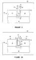
- FIG. 1Ais a cross-sectional view of a contact hole that has been etched through an insulative layer to an underlying semiconductor substrate.
- FIG. 1Bis a cross-sectional view of the contact hole of FIG. 1A , comprising titanium and titanium silicide film.
- FIG. 2is a cross-sectional view of the contact hole of FIG. 1A , comprising a film of second reducing agent.
- FIG. 3Ais a cross-sectional view of a contact hole as in FIG. 1A , including additional structures according to an embodiment of the invention.
- FIG. 3Bis a block diagram of a memory.
- wafer and substrate used in the following descriptioninclude any semiconductor-based structure having an exposed surface with which to form the integrated circuit structure of the invention. Wafer and substrate are used interchangeably to refer to semiconductor structures during processing, and may include other layers that have been fabricated thereupon.
- Both wafer and substrateinclude doped and undoped semiconductors, epitaxial semiconductor layers supported by a base semiconductor or insulator, as well as other semiconductor structures well known to one skilled in the art.
- doped and undoped semiconductorsepitaxial semiconductor layers supported by a base semiconductor or insulator, as well as other semiconductor structures well known to one skilled in the art.
- the following detailed descriptionis, therefore, not to be taken in a limiting sense, and the scope of the present invention is defined only by the appended claims.
- a contact hole 10is etched through an insulating layer 12 , such as borophosphosilicate glass (BPSG) or silicon dioxide (SiO 2 ).
- BPSGborophosphosilicate glass
- SiO 2silicon dioxide
- CVDChemical vapor deposition
- the conformal layerhas a step coverage of at least one hundred percent in the contact hole 10 , even for a high aspect ratio contact hole (i.e., a contact hole that is much deeper than it is wide).
- a low resistance layer of titanium or titanium alloy 16is formed on the insulating layer 12 , as shown in FIG. 1B .
- a portion of the layer 16is formed as a low resistance device contact 18 of titanium silicide over the active region 17 .
- a cold wall-hot substrate reactoris used to form the conformal layer of titanium or titanium alloy.
- a cold wall-hot substrate reactoris used for blanket depositions as this design is efficient in regard to precursor consumption.
- a conformal film of a seed layer 22 comprising zincis deposited on the insulator 12 and substrate 14 , as shown in FIG. 2 .
- the seed layer 22is formed with CVD by combining a first reducing agent 24 with a first precursor 26 , which are injected into the CVD reactor which is represented in block form at 29 .
- the seed layer 22 that is zincmay be formed by combining a first precursor 26 that is a dialkyl zinc or trimethyl zinc compound with a reducing agent 24 that is hydrogen.
- the integrated circuit 19is mounted on a substrate holder in the CVD reactor 29 .
- the substrate 14is heated to a temperature within a range of approximately 100 to 600 degrees Celsius and at a pressure approximately between 1 millitorr and 1 atmosphere.
- the temperaturemay range from approximately 300 to 550 degrees Celsius, or approximately 350 to 450 degrees Celsius.
- the temperatureis approximately 400 degrees Celsius.
- the pressuremay range from approximately 10 millitorr to 100 torr.
- the pressureis approximately 1 torr.
- a carrier gas of helium, argon or nitrogenmay be used at a flow rate of between approximately 1 and 200 sccm. Alternatively, the flow rate may range between approximately 20 sccm and 1 liter.
- the pressureis approximately 200 sccm.
- the first precursor 26 and the reducing agent 24contact the heated silicon base layer and insulating layer 12 , and form the seed layer 22 on the integrated circuit 19 .
- This chemical process (I)is exemplified below: ZnR 2 (gas)+H 2 (gas) ⁇ Zn(solid)+alkanes(gas), (I)
- Ris an alkyl group
- First reaction products 28such as gaseous alkanes, resulting from the formation of the seed layer 22 exit from the CVD reactor 29 through an exhaust manifold.
- the thickness of the seed layer 22 formed on the integrated circuit 19is between approximately 5 and 50 angstroms. However, the present invention envisions forming a seed layer 22 that is thicker.
- the seed layer 22is converted to a layer 16 of titanium or a titanium alloy.
- a titanium precursor 32such as titanium tetrachloride, is combined with the seed layer 22 by CVD to form a conformal layer 16 of titanium or titanium alloy in lieu of the seed layer 22 .
- the integrated circuit 19is mounted and heated in the CVD reactor 29 to a temperature within a range of approximately 100 to 600 degrees Celsius and at a pressure approximately between 1 millitorr and 1 atmosphere.
- the temperaturemay range from approximately 100 to 700 degrees Celsius, approximately 300 to 550 degrees Celsius, or approximately 350 to 450 degrees Celsius. In one embodiment, the temperature is approximately 400 degrees Celsius.
- the pressuremay range from approximately 10 millitorr to 100 torr. In one embodiment, the pressure is approximately 1 torr.
- a carrier gas of helium, argon or nitrogenmay be used at a flow of between approximately 1 and 200 sccm. Alternatively, the flow rate may range between approximately 20 sccm and 1 liter.
- the pressureis approximately 200 sccm.
- the titanium precursor 32contacts the seed layer 22 on the integrated circuit 19 , the compounds form a conformal layer 16 of titanium or a titanium alloy.
- the chemical process (II)is exemplified below: TiCl 4 (gas)+Zn(solid) ⁇ Ti(solid)+ZnCl 2 (gas) (II)
- Second reaction products 34 resulting from the formation of the titanium or titanium alloyexit from the CVD reactor 29 through the exhaust manifold.
- Part or all of the seed layer 22is converted to a layer 16 of titanium or titanium alloy. If this process step is conducted for a sufficient period of time, all of the seed layer 22 will be converted to a layer 16 of titanium. However, if not all of the seed layer 22 is converted to a layer 16 of titanium, a layer 16 of titanium alloy, including the seed layer 22 , will be formed on the integrated circuit 19 . These steps may be repeated to form thicker layers.
- the layer 16 of titanium or titanium alloycan be formed during a single CVD step, as exemplified by chemical process (III) below: TiCl 4 +Zn(source) ⁇ Ti+ZnCl 2 (III)
- the zinccan be provided from one of many types of sources, including gaseous and solid sources.
- the seed and titanium layers 22 , 16can be formed substantially simultaneously.
- the titanium or titanium alloy layer 16can be formed by combining a first precursor 26 , such as a dialkyl or trimethyl zinc compound, with a reducing agent 24 , such as hydrogen, and a titanium precursor 32 , such as titanium tetrachloride.
- the integrated circuit 19is mounted and heated in the CVD reactor 29 to a temperature within a range of approximately 100 to 600 degrees Celsius at a pressure of approximately between 1 millitorr and 1 atmosphere.
- the temperaturemay range from approximately 100 to 700 degrees Celsius, approximately 300 to 550 degrees Celsius, or approximately 350 to 450 degrees Celsius. In one embodiment, the temperature is approximately 400 degrees Celsius.
- the pressuremay range from approximately 10 millitorr to 100 torr. In one embodiment, the pressure is approximately 1 torr.
- a carrier gas of helium, argon or nitrogenmay be used at a flow rate of between approximately 1 and 200 sccm. Alternatively, the flow rate may range between approximately 20 sccm and 1 liter.
- the pressureis approximately 200 sccm.
- the first precursor 26 and the reducing agent 24contact the heated silicon base layer and insulating layer 12 , they form the seed layer 22 on the integrated circuit 19 .
- the titanium precursor 32contacts the seed layer 22 , a conformal layer 16 of titanium or titanium alloy is formed on the integrated circuit.
- the resulting layer 16 of titanium or titanium alloyhas a thickness between approximately 5 and 50 angstroms.
- the present inventionenvisions forming a thicker layer 16 titanium or titanium alloy.
- reaction products 28 , 34exit from the CVD reactor 29 through the exhaust manifold.
- the integrated circuit 19is annealed at a temperature of between approximately 250 to 750 degrees Celsius. Alternatively, the temperature may range from approximately 250 to 800 degrees Celsius. In one embodiment, the temperature is approximately 700 degrees Celsius.
- the titanium in the layer 16 of titanium or titanium alloy proximate to the siliconis converted to titanium silicide (TiSi, TiSi 2 , Ti 3 Si 5 or combinations thereof) to form the low resistance device contact 18 .
- the annealis not required.
- the viacomprises a tungsten or aluminum fill 42 on top of the layer 16 which is formed on top of a conductor (also represented by reference number 17 ) with an optional TiN layer 40 between layer 16 and the fill material 42 .
- the low resistance device contact 18 of titanium silicidemay be formed over the active region 17 when the layer 16 of titanium or titanium alloy is formed by CVD on the integrated circuit 19 at a temperature of between approximately 250 to 750 degrees Celsius. Alternatively, the temperature may range from approximately 250 to 800 degrees Celsius. In one embodiment, the temperature is approximately 700 degrees Celsius.
- additional metal layerssuch as titanium nitride and tungsten, may be subsequently formed over the device contact 18 and layer 16 of titanium or titanium alloy.
- the integrated circuit 19is a memory 300 in FIG. 3B , such as a dynamic random access memory.
- the memory 300may include an array of memory cells 302 , control circuit 304 , I/O circuit, word line decoder 308 , digit, or bit, line decoder 310 , and sense amplifier 312 coupled in a manner known to one skilled in the art.
- Each of the aforementioned elements of the memory 300includes contacts 18 and layers 16 of titanium, or titanium alloy, formed in the manner described above.
- the first precursor 26is an alkane of the form MR x , where M is an element selected from the group consisting of zinc, cadmium, mercury, aluminum, gallium, indium, tin, silicon, germanium, lead, arsenic and antimony; R is an alkyl group; and x is some integer value determined by the valence of M.
- the value of xis generally equal to a valence of M, e.g., when M has a valence of 3 as does aluminum, x equals 3.
- Mmay be capable of having more than one valence.
- Such alkane precursorsmay be used to form the seed layer 22 .
- Chemical process (I) for the formation of seed layer 22may then be written in its more general form: MR x (gas)+H 2 (gas) ⁇ M(solid)+alkanes(gas), (I) wherein:
- chemical process (III)may be written more generally as: TiCl 4 +M(source) ⁇ Ti+MCl x (III) wherein:
- chemical process (IV)may be written more generally as: MR x (gas)+H 2 (gas)+TiCl 4 (gas) ⁇ Ti(solid)+MCl x (gas)+alkanes(gas), (IV) wherein:
- the various embodiments of the present inventionprovide high step coverage, low resistivity titanium silicide device contacts to silicon, or titanium contacts to metal at the via level, formed at a relatively low temperature.
- Use of the various alkane precursorspermits formation of a titanium layer without depletion of an underlying silicon or other base layer.
- TDMATtetradimethyl amino titanium
- the present inventionmay be implemented with any CVD apparatus 29 , including hot wall reactors, cold wall reactors, radiation beam assisted reactors, plasma-assisted reactors, and the like.
- the seed layer 22may be formed in any manner which provides a desired thickness film.
Landscapes
- Chemical & Material Sciences (AREA)
- Engineering & Computer Science (AREA)
- Physics & Mathematics (AREA)
- Condensed Matter Physics & Semiconductors (AREA)
- General Physics & Mathematics (AREA)
- Manufacturing & Machinery (AREA)
- Computer Hardware Design (AREA)
- Microelectronics & Electronic Packaging (AREA)
- Power Engineering (AREA)
- General Chemical & Material Sciences (AREA)
- Chemical Kinetics & Catalysis (AREA)
- Materials Engineering (AREA)
- Mechanical Engineering (AREA)
- Metallurgy (AREA)
- Organic Chemistry (AREA)
- Plasma & Fusion (AREA)
- Crystallography & Structural Chemistry (AREA)
- Internal Circuitry In Semiconductor Integrated Circuit Devices (AREA)
- Electrodes Of Semiconductors (AREA)
- Chemical Vapour Deposition (AREA)
- Semiconductor Memories (AREA)
Abstract
Description
This application is a divisional of U.S. application Ser. No. 11/146,609, filed Jun. 7, 2005 now U.S. Pat. No. 7,443,032, which is a continuation of U.S. application Ser. No. 09/941,125, filed Aug. 28, 2001, now issued as U.S. Pat. No. 6,830,838, which is a divisional of U.S. application Ser. No. 09/489,187, filed Jan. 20, 2000, now issued as U.S. Pat. No. 6,284,316, which is a continuation-in-part of U.S. application Ser. No. 09/030,705, filed Feb. 25, 1998, now issued as U.S. Pat. No. 6,143,362. These applications are incorporated herein by reference.
The present invention relates to a method for manufacturing semiconductor devices, and more particularly, to a method for depositing titanium layers on a substrate.
Device density in integrated circuits (ICs) is constantly being increased. To enable the increase in density, device dimensions are being reduced. As the dimensions of device contacts get smaller, device contact resistance increases, and device performance is adversely affected. Methods for decreasing device contact resistance in ICs are needed to obtain enhanced device and IC performance.
Device contacts with reduced resistance may be created by forming certain metals on a silicon semiconductor base layer. These metals react with the underlying silicon, for example, to form silicides. Silicide device contacts are desirable because they reduce the native oxide on silicon. The native oxide is undesirable because it increases the contact resistance.
In one embodiment, titanium is used to form silicide device contacts for two reasons. First, titanium silicide has superior gettering qualities. Also, titanium silicide forms low resistance contacts on both polysilicon and single-crystal silicon.
Titanium silicide device contacts are normally formed with the following process. First, a thin layer of titanium is formed on top of the silicon base layer, such as a substrate. The titanium adjoins active regions exposed by contact holes in an isolating layer, such as an oxide, above the silicon base layer. Then, the silicon base layer is annealed. As a result, the titanium reacts with the active regions of silicon to form titanium silicide.
However, because titanium cannot be readily deposited in a pure form, additional processing steps are required to form titanium silicide device contacts. Titanium precursors, such as titanium tetrachloride, are commonly available and can be used to form titanium. Titanium tetrachloride, though, can only be reduced at temperatures exceeding 1000 degrees Celsius with certain reducing agents. At these temperatures, the silicon base layer will be damaged. Therefore, there is a need for a method of forming titanium from titanium precursors at lower temperatures.
Furthermore, the resistance of device contacts can be adversely increased by conductive layers coupled between the device contacts and other components. The conductive layers may be formed by the same metal layer used to form the device contacts. As device dimensions shrink, the contact holes become relatively deeper and narrower. Also, the walls of the contact holes become steeper, and closer to vertical. As a result, most metal deposition techniques form conductive layers having relatively small step coverage, and hence relatively high resistance. Step coverage is the ratio of the minimum thickness of a film as it crosses a step, to the nominal thickness of the film on flat regions, where thickness is generally measured perpendicular to the surfaces of the step and flat regions, and where the resultant value is usually expressed as a percentage. Thus, the effective contact resistance is increased at lower values of step coverage. Therefore, there is also a need for a method of forming conductive layers having increased step coverage to reduce effective device contact resistance.
Conformal layers of titanium having good step coverage have been previously formed at lower temperatures with chemical vapor deposition. Such techniques are disclosed in U.S. Pat. Nos. 5,173,327, 5,273,783 and 5,278,100, which are hereby incorporated by reference. However, alternative, effective and efficient techniques for forming titanium films are desired.
The present invention provides a method, and a corresponding resulting structure, for forming conformal titanium films supported on a substrate of an integrated circuit (IC) by forming a seed layer supported by the substrate, and then reducing a titanium precursor with the seed layer. In one embodiment, the seed layer comprises a main group element selected from the group consisting of zinc, cadmium, mercury, aluminum, gallium, indium, tin, silicon, germanium, lead, arsenic and antimony. The seed layer is formed by combining a first precursor and a reducing agent by chemical vapor deposition (CVD). Then, titanium is formed by combining a second precursor with the seed layer by CVD.
In another embodiment, the present invention may further comprise the step of annealing the titanium to form titanium silicide.
In another embodiment, forming the seed layer further comprises forming a seed layer according to the following chemical process (I):
MRx+H2→M+alkanes,
wherein:
MRx+H2→M+alkanes,
wherein:
- M is a main group element selected from the group consisting of zinc, cadmium, mercury, aluminum, gallium, indium, tin, silicon, germanium, lead, arsenic and antimony;
- R is an alkyl group; and
- x is some integer value determined by the valence of M.
In one embodiment, chemical process (I) is performed at a temperature between approximately 100 and 600 degrees Celsius.
In yet another embodiment, the step of forming titanium further comprises the step of combining the seed layer with the second precursor that is titanium tetrachloride according to the following chemical process (II):
TiCl4+M→Ti+MClx
In one embodiment, chemical process (II) is performed at a temperature between approximately 100 and 600 degrees Celsius.
TiCl4+M→Ti+MClx
In one embodiment, chemical process (II) is performed at a temperature between approximately 100 and 600 degrees Celsius.
In yet another embodiment, titanium may be formed in a single step according to the following chemical process (III):
TiCl4+M(source)→Ti+MClx
In one embodiment, chemical process (III) is performed at a temperature between approximately 100 and 700 degrees Celsius.
TiCl4+M(source)→Ti+MClx
In one embodiment, chemical process (III) is performed at a temperature between approximately 100 and 700 degrees Celsius.
In yet a further embodiment, the present invention may be an IC comprising a layer of a titanium alloy, coupled to a titanium silicide contact. In yet another embodiment, the present invention may be a memory comprising a memory array operatively coupled to a control circuit and an I/O circuit. The memory array, control circuit and I/O circuit comprise a layer of a titanium alloy coupled to titanium silicide contacts. In yet another embodiment, the titanium alloy may comprise titanium and an element selected from the group consisting of zinc, cadmium, mercury, aluminum, gallium, indium, tin, silicon, germanium, lead, arsenic and antimony. In still another embodiment, the titanium alloy may comprise titanium and zinc.
It is a benefit of the present invention that high step coverage metal layers can be formed. Further features and advantages of the present invention, as well as the structure and operations of various embodiments of the present invention, are described in detail below with reference to the accompanying drawings.
In the following detailed description of the preferred embodiments, reference is made to the accompanying drawings which form a part hereof, and in which is shown by way of illustration specific preferred embodiments in which the inventions may be practiced. These embodiments are described in sufficient detail to enable persons skilled in the art to practice the invention, and it is to be understood that other embodiments may be utilized and that logical, mechanical and electrical changes may be made without departing from the spirit and scope of the present invention. The terms wafer and substrate used in the following description include any semiconductor-based structure having an exposed surface with which to form the integrated circuit structure of the invention. Wafer and substrate are used interchangeably to refer to semiconductor structures during processing, and may include other layers that have been fabricated thereupon. Both wafer and substrate include doped and undoped semiconductors, epitaxial semiconductor layers supported by a base semiconductor or insulator, as well as other semiconductor structures well known to one skilled in the art. The following detailed description is, therefore, not to be taken in a limiting sense, and the scope of the present invention is defined only by the appended claims.
The subsequently described methods will be in the context of using zinc as a metal seed layer. However, other seed layers are suitable for use with the various embodiments of the invention, as will be described.
In order to manufacture a device contact in anintegrated circuit 19, acontact hole 10, as shown inFIG. 1A , is etched through an insulatinglayer 12, such as borophosphosilicate glass (BPSG) or silicon dioxide (SiO2). As a result, anactive region 17 of underlying semiconductor base layer orsubstrate 14, is exposed. A device contact is then formed on the exposedactive region 17 in the following manner.
Chemical vapor deposition (CVD) is used to form a conformal layer of titanium or titanium alloy on theintegrated circuit 19 by a subsequently described method. CVD is further described in U.S. Pat. No. 5,278,100. In one embodiment, the conformal layer has a step coverage of at least one hundred percent in thecontact hole 10, even for a high aspect ratio contact hole (i.e., a contact hole that is much deeper than it is wide). As a result, a low resistance layer of titanium ortitanium alloy 16 is formed on the insulatinglayer 12, as shown inFIG. 1B . A portion of thelayer 16 is formed as a lowresistance device contact 18 of titanium silicide over theactive region 17.
In another embodiment, a cold wall-hot substrate reactor is used to form the conformal layer of titanium or titanium alloy. In one embodiment, a cold wall-hot substrate reactor is used for blanket depositions as this design is efficient in regard to precursor consumption. In one embodiment, first, a conformal film of aseed layer 22 comprising zinc is deposited on theinsulator 12 andsubstrate 14, as shown inFIG. 2 . Theseed layer 22 is formed with CVD by combining a first reducingagent 24 with afirst precursor 26, which are injected into the CVD reactor which is represented in block form at29. In another embodiment, theseed layer 22 that is zinc may be formed by combining afirst precursor 26 that is a dialkyl zinc or trimethyl zinc compound with a reducingagent 24 that is hydrogen.
When performing this step, theintegrated circuit 19 is mounted on a substrate holder in theCVD reactor 29. Thesubstrate 14 is heated to a temperature within a range of approximately 100 to 600 degrees Celsius and at a pressure approximately between 1 millitorr and 1 atmosphere. Alternatively, the temperature may range from approximately 300 to 550 degrees Celsius, or approximately 350 to 450 degrees Celsius. In one embodiment, the temperature is approximately 400 degrees Celsius. Also, alternatively, the pressure may range from approximately 10 millitorr to 100 torr. In one embodiment, the pressure is approximately 1 torr. A carrier gas of helium, argon or nitrogen may be used at a flow rate of between approximately 1 and 200 sccm. Alternatively, the flow rate may range between approximately 20 sccm and 1 liter. In one embodiment, the pressure is approximately 200 sccm. Thefirst precursor 26 and the reducingagent 24 contact the heated silicon base layer and insulatinglayer 12, and form theseed layer 22 on theintegrated circuit 19. This chemical process (I) is exemplified below:
ZnR2(gas)+H2(gas)→Zn(solid)+alkanes(gas), (I)
ZnR2(gas)+H2(gas)→Zn(solid)+alkanes(gas), (I)
where R is an alkyl group.
Next, theseed layer 22 is converted to alayer 16 of titanium or a titanium alloy. As illustrated inFIG. 3A , atitanium precursor 32, such as titanium tetrachloride, is combined with theseed layer 22 by CVD to form aconformal layer 16 of titanium or titanium alloy in lieu of theseed layer 22.
When performing this step, theintegrated circuit 19 is mounted and heated in theCVD reactor 29 to a temperature within a range of approximately 100 to 600 degrees Celsius and at a pressure approximately between 1 millitorr and 1 atmosphere. Alternatively, the temperature may range from approximately 100 to 700 degrees Celsius, approximately 300 to 550 degrees Celsius, or approximately 350 to 450 degrees Celsius. In one embodiment, the temperature is approximately 400 degrees Celsius. Also, alternatively, the pressure may range from approximately 10 millitorr to 100 torr. In one embodiment, the pressure is approximately 1 torr. A carrier gas of helium, argon or nitrogen may be used at a flow of between approximately 1 and 200 sccm. Alternatively, the flow rate may range between approximately 20 sccm and 1 liter. In one embodiment, the pressure is approximately 200 sccm. When thetitanium precursor 32 contacts theseed layer 22 on theintegrated circuit 19, the compounds form aconformal layer 16 of titanium or a titanium alloy. The chemical process (II) is exemplified below:
TiCl4(gas)+Zn(solid)→Ti(solid)+ZnCl2(gas) (II)
TiCl4(gas)+Zn(solid)→Ti(solid)+ZnCl2(gas) (II)
In another embodiment, thelayer 16 of titanium or titanium alloy can be formed during a single CVD step, as exemplified by chemical process (III) below:
TiCl4+Zn(source)→Ti+ZnCl2 (III)
The zinc can be provided from one of many types of sources, including gaseous and solid sources. In one embodiment of such a single CVD step, the seed andtitanium layers titanium alloy layer 16 can be formed by combining afirst precursor 26, such as a dialkyl or trimethyl zinc compound, with a reducingagent 24, such as hydrogen, and atitanium precursor 32, such as titanium tetrachloride. When performing the CVD step, theintegrated circuit 19 is mounted and heated in theCVD reactor 29 to a temperature within a range of approximately 100 to 600 degrees Celsius at a pressure of approximately between 1 millitorr and 1 atmosphere. Alternatively, the temperature may range from approximately 100 to 700 degrees Celsius, approximately 300 to 550 degrees Celsius, or approximately 350 to 450 degrees Celsius. In one embodiment, the temperature is approximately 400 degrees Celsius. Also, alternatively, the pressure may range from approximately 10 millitorr to 100 torr. In one embodiment, the pressure is approximately 1 torr. A carrier gas of helium, argon or nitrogen may be used at a flow rate of between approximately 1 and 200 sccm. Alternatively, the flow rate may range between approximately 20 sccm and 1 liter. In one embodiment, the pressure is approximately 200 sccm. When thefirst precursor 26 and the reducingagent 24 contact the heated silicon base layer and insulatinglayer 12, they form theseed layer 22 on theintegrated circuit 19. Then, when thetitanium precursor 32 contacts theseed layer 22, aconformal layer 16 of titanium or titanium alloy is formed on the integrated circuit. The resultinglayer 16 of titanium or titanium alloy has a thickness between approximately 5 and 50 angstroms. However, the present invention envisions forming athicker layer 16 titanium or titanium alloy. The chemical process (IV) is exemplified below:
ZnR2(gas)+H2(gas)+TiCl4(gas)→Ti(solid)+ZnCl2(gas)+alkanes(gas), (IV)
where R is an alkyl group.
TiCl4+Zn(source)→Ti+ZnCl2 (III)
The zinc can be provided from one of many types of sources, including gaseous and solid sources. In one embodiment of such a single CVD step, the seed and
ZnR2(gas)+H2(gas)+TiCl4(gas)→Ti(solid)+ZnCl2(gas)+alkanes(gas), (IV)
where R is an alkyl group.
Thereaction products CVD reactor 29 through the exhaust manifold.
Subsequently, theintegrated circuit 19 is annealed at a temperature of between approximately 250 to 750 degrees Celsius. Alternatively, the temperature may range from approximately 250 to 800 degrees Celsius. In one embodiment, the temperature is approximately 700 degrees Celsius. As a result, the titanium in thelayer 16 of titanium or titanium alloy proximate to the silicon is converted to titanium silicide (TiSi, TiSi2, Ti3Si5or combinations thereof) to form the lowresistance device contact 18. For via level applications, the anneal is not required. The via comprises a tungsten or aluminum fill42 on top of thelayer 16 which is formed on top of a conductor (also represented by reference number17) with anoptional TiN layer 40 betweenlayer 16 and thefill material 42.
In yet another embodiment, the lowresistance device contact 18 of titanium silicide may be formed over theactive region 17 when thelayer 16 of titanium or titanium alloy is formed by CVD on theintegrated circuit 19 at a temperature of between approximately 250 to 750 degrees Celsius. Alternatively, the temperature may range from approximately 250 to 800 degrees Celsius. In one embodiment, the temperature is approximately 700 degrees Celsius. Upondevice contact 18 formation, additional metal layers, such as titanium nitride and tungsten, may be subsequently formed over thedevice contact 18 andlayer 16 of titanium or titanium alloy.
In another embodiment, theintegrated circuit 19 is amemory 300 inFIG. 3B , such as a dynamic random access memory. Thememory 300 may include an array ofmemory cells 302,control circuit 304, I/O circuit,word line decoder 308, digit, or bit,line decoder 310, andsense amplifier 312 coupled in a manner known to one skilled in the art. Each of the aforementioned elements of thememory 300 includescontacts 18 and layers16 of titanium, or titanium alloy, formed in the manner described above.
As noted above, other seed layers are suitable for use with the various embodiments of the invention. In one embodiment, thefirst precursor 26 is an alkane of the form MRx, where M is an element selected from the group consisting of zinc, cadmium, mercury, aluminum, gallium, indium, tin, silicon, germanium, lead, arsenic and antimony; R is an alkyl group; and x is some integer value determined by the valence of M. The value of x is generally equal to a valence of M, e.g., when M has a valence of 3 as does aluminum, x equals 3. M may be capable of having more than one valence. Such alkane precursors may be used to form theseed layer 22. Chemical process (I) for the formation ofseed layer 22 may then be written in its more general form:
MRx(gas)+H2(gas)→M(solid)+alkanes(gas), (I)
wherein:
MRx(gas)+H2(gas)→M(solid)+alkanes(gas), (I)
wherein:
- M is an element selected from the group consisting of zinc, cadmium, mercury, aluminum, gallium, indium, tin, silicon, germanium, lead, arsenic and antimony;
- R is an alkyl group; and
- x is some integer value equal to the valence of M.
In similar fashion, chemical process (II) for the formation of thelayer 16 of titanium or titanium alloy may be written more generally as:
TiCl4(gas)+M(solid)→Ti(solid)+MClx(gas) (II)
wherein:
TiCl4(gas)+M(solid)→Ti(solid)+MClx(gas) (II)
wherein:
- M is an element selected from the group consisting of zinc, cadmium, mercury, aluminum, gallium, indium, tin, silicon, germanium, lead, arsenic and antimony; and
- x is some integer value equal to the valence of M.
In another embodiment, where the formation of thelayer 16 of titanium or titanium alloy is performed in a single step, chemical process (III) may be written more generally as:
TiCl4+M(source)→Ti+MClx (III)
wherein:
TiCl4+M(source)→Ti+MClx (III)
wherein:
- M is an element selected from the group consisting of zinc, cadmium, mercury, aluminum, gallium, indium, tin, silicon, germanium, lead, arsenic and antimony; and
- x is some integer value equal to the valence of M.
In a further embodiment, where the formation of thelayer 16 of titanium or titanium alloy is performed in a single CVD step, chemical process (IV) may be written more generally as:
MRx(gas)+H2(gas)+TiCl4(gas)→Ti(solid)+MClx(gas)+alkanes(gas), (IV)
wherein:
MRx(gas)+H2(gas)+TiCl4(gas)→Ti(solid)+MClx(gas)+alkanes(gas), (IV)
wherein:
- M is an element selected from the group consisting of zinc, cadmium, mercury, aluminum, gallium, indium, tin, silicon, germanium, lead, arsenic and antimony;
- R is an alkyl group; and
- x is some integer value equal to the valence of M.
The various embodiments of the present invention provide high step coverage, low resistivity titanium silicide device contacts to silicon, or titanium contacts to metal at the via level, formed at a relatively low temperature. Use of the various alkane precursors permits formation of a titanium layer without depletion of an underlying silicon or other base layer.
It is to be understood that the above description is intended to be illustrative, and not restrictive. Many other embodiments will be apparent to those of skill in the art upon reviewing the above description. For example, other titanium precursors, such as tetradimethyl amino titanium (TDMAT) can be used to formlayers 16 anddevice contacts 18. Additionally, the present invention may be implemented with anyCVD apparatus 29, including hot wall reactors, cold wall reactors, radiation beam assisted reactors, plasma-assisted reactors, and the like. Furthermore, theseed layer 22 may be formed in any manner which provides a desired thickness film. Hence, the scope of the invention should, therefore, be determined with reference to the appended claims, along with the full scope of equivalents to which such claims are entitled.
Claims (7)
1. A memory device, comprising: a memory array; a control circuit operatively coupled to the memory array; and an input/output circuit operatively coupled to the memory array, wherein at least one of the memory array, the control circuit, or the input/output circuit further comprises a via having:
a layer of a titanium alloy formed to overlay walls of a contact hole, wherein the titanium alloy comprises titanium and an element selected from the group consisting of zinc, cadmium, mercury, aluminum, gallium, indium, tin, silicon, germanium, lead, arsenic and antimony,
a titanium silicide contact formed in the layer of titanium alloy and having a composition that is different than the layer of titanium alloy, the titanium silicide contact being directly coupled to the layer of titanium alloy, and a fill coupled to the layer of titanium alloy, the fill comprising a metal selected from the group consisting of tungsten and aluminum.
2. The memory ofclaim 1 , wherein the titanium has an atomic percentage of from about 50% to about 90% of the titanium alloy.
3. The memory ofclaim 1 , wherein the fill has a level approximately equal to a height of the via.
4. A memory device, comprising: a memory array; a control circuit operatively coupled to the memory array; and an input/output circuit operatively coupled to the memory array, wherein at least one of the memory array, the control circuit, or the input/output circuit comprises:
a layer of a titanium alloy formed to overlay walls of a contact hole, wherein the titanium alloy comprises titanium and an element selected from the group consisting of zinc, cadmium, mercury, aluminum, gallium, indium, tin, silicon, germanium, lead, arsenic and antimony; and
a titanium silicide contact formed in the layer of titanium alloy and having a composition that is different than the layer of titanium alloy, the titanium silicide contact being directly coupled to the layer of titanium alloy and produced using a method comprising:
forming a seed layer within the contact opening by combining a first precursor with a first reducing agent, and;
forming the titanium alloy layer within the contact opening by combining a titanium-containing precursor with the seed layer to form a titanium alloy layer having at least 100% step coverage within the contact.
5. The memory ofclaim 4 , wherein the titanium has an atomic percentage of from about 50% to about 90% of the titanium alloy.
6. The memory ofclaim 4 , further comprising:
a contact hole conductive plug formed from selective deposition of a conductive material selected from the list including tungsten and aluminum.
7. The memory ofclaim 6 , further comprising:
a titanium nitride layer disposed underneath the contact hole conductive plug and above the titanium silicide.
Priority Applications (1)
| Application Number | Priority Date | Filing Date | Title |
|---|---|---|---|
| US12/249,774US8456007B2 (en) | 1998-02-25 | 2008-10-10 | Chemical vapor deposition of titanium |
Applications Claiming Priority (5)
| Application Number | Priority Date | Filing Date | Title |
|---|---|---|---|
| US09/030,705US6143362A (en) | 1998-02-25 | 1998-02-25 | Chemical vapor deposition of titanium |
| US09/489,187US6284316B1 (en) | 1998-02-25 | 2000-01-20 | Chemical vapor deposition of titanium |
| US09/941,125US6830838B2 (en) | 1998-02-25 | 2001-08-28 | Chemical vapor deposition of titanium |
| US11/146,609US7443032B2 (en) | 1998-02-25 | 2005-06-07 | Memory device with chemical vapor deposition of titanium for titanium silicide contacts |
| US12/249,774US8456007B2 (en) | 1998-02-25 | 2008-10-10 | Chemical vapor deposition of titanium |
Related Parent Applications (1)
| Application Number | Title | Priority Date | Filing Date |
|---|---|---|---|
| US11/146,609DivisionUS7443032B2 (en) | 1998-02-25 | 2005-06-07 | Memory device with chemical vapor deposition of titanium for titanium silicide contacts |
Publications (2)
| Publication Number | Publication Date |
|---|---|
| US20090039517A1 US20090039517A1 (en) | 2009-02-12 |
| US8456007B2true US8456007B2 (en) | 2013-06-04 |
Family
ID=26706372
Family Applications (7)
| Application Number | Title | Priority Date | Filing Date |
|---|---|---|---|
| US09/489,187Expired - LifetimeUS6284316B1 (en) | 1998-02-25 | 2000-01-20 | Chemical vapor deposition of titanium |
| US09/940,917Expired - Fee RelatedUS6940172B2 (en) | 1998-02-25 | 2001-08-28 | Chemical vapor deposition of titanium |
| US09/941,123Expired - Fee RelatedUS6903462B2 (en) | 1998-02-25 | 2001-08-28 | Chemical vapor deposition of titanium |
| US09/941,125Expired - Fee RelatedUS6830838B2 (en) | 1998-02-25 | 2001-08-28 | Chemical vapor deposition of titanium |
| US09/940,980Expired - Fee RelatedUS6830820B2 (en) | 1998-02-25 | 2001-08-28 | Chemical vapor deposition of titanium |
| US11/146,609Expired - Fee RelatedUS7443032B2 (en) | 1998-02-25 | 2005-06-07 | Memory device with chemical vapor deposition of titanium for titanium silicide contacts |
| US12/249,774Expired - Fee RelatedUS8456007B2 (en) | 1998-02-25 | 2008-10-10 | Chemical vapor deposition of titanium |
Family Applications Before (6)
| Application Number | Title | Priority Date | Filing Date |
|---|---|---|---|
| US09/489,187Expired - LifetimeUS6284316B1 (en) | 1998-02-25 | 2000-01-20 | Chemical vapor deposition of titanium |
| US09/940,917Expired - Fee RelatedUS6940172B2 (en) | 1998-02-25 | 2001-08-28 | Chemical vapor deposition of titanium |
| US09/941,123Expired - Fee RelatedUS6903462B2 (en) | 1998-02-25 | 2001-08-28 | Chemical vapor deposition of titanium |
| US09/941,125Expired - Fee RelatedUS6830838B2 (en) | 1998-02-25 | 2001-08-28 | Chemical vapor deposition of titanium |
| US09/940,980Expired - Fee RelatedUS6830820B2 (en) | 1998-02-25 | 2001-08-28 | Chemical vapor deposition of titanium |
| US11/146,609Expired - Fee RelatedUS7443032B2 (en) | 1998-02-25 | 2005-06-07 | Memory device with chemical vapor deposition of titanium for titanium silicide contacts |
Country Status (1)
| Country | Link |
|---|---|
| US (7) | US6284316B1 (en) |
Cited By (3)
| Publication number | Priority date | Publication date | Assignee | Title |
|---|---|---|---|---|
| US9390909B2 (en) | 2013-11-07 | 2016-07-12 | Novellus Systems, Inc. | Soft landing nanolaminates for advanced patterning |
| US9478438B2 (en) | 2014-08-20 | 2016-10-25 | Lam Research Corporation | Method and apparatus to deposit pure titanium thin film at low temperature using titanium tetraiodide precursor |
| US9478411B2 (en) | 2014-08-20 | 2016-10-25 | Lam Research Corporation | Method to tune TiOx stoichiometry using atomic layer deposited Ti film to minimize contact resistance for TiOx/Ti based MIS contact scheme for CMOS |
Families Citing this family (35)
| Publication number | Priority date | Publication date | Assignee | Title |
|---|---|---|---|---|
| US6841203B2 (en)* | 1997-12-24 | 2005-01-11 | Tokyo Electron Limited | Method of forming titanium film by CVD |
| US6284316B1 (en)* | 1998-02-25 | 2001-09-04 | Micron Technology, Inc. | Chemical vapor deposition of titanium |
| KR100304714B1 (en)* | 1999-10-20 | 2001-11-02 | 윤종용 | Method for fabricating metal layer of semiconductor device using metal-halide gas |
| US6379383B1 (en) | 1999-11-19 | 2002-04-30 | Advanced Bio Prosthetic Surfaces, Ltd. | Endoluminal device exhibiting improved endothelialization and method of manufacture thereof |
| WO2002038080A2 (en) | 2000-11-07 | 2002-05-16 | Advanced Bio Prosthetic Surfaces, Ltd. | Endoluminal stent, self-fupporting endoluminal graft and methods of making same |
| US9076843B2 (en) | 2001-05-22 | 2015-07-07 | Novellus Systems, Inc. | Method for producing ultra-thin tungsten layers with improved step coverage |
| JP2004007270A (en)* | 2002-05-31 | 2004-01-08 | Panasonic Communications Co Ltd | Adsl modem apparatus, adsl communication apparatus, and synchronization adjustment method for adsl communication |
| US7311942B2 (en)* | 2002-08-29 | 2007-12-25 | Micron Technology, Inc. | Method for binding halide-based contaminants during formation of a titanium-based film |
| AU2003270817B2 (en) | 2002-09-26 | 2009-09-17 | Vactronix Scientific, Llc | High strength vacuum deposited nitionol alloy films, medical thin film graft materials and method of making same |
| KR100578221B1 (en)* | 2004-05-06 | 2006-05-12 | 주식회사 하이닉스반도체 | Method for manufacturing semiconductor device having diffusion barrier |
| US9202758B1 (en)* | 2005-04-19 | 2015-12-01 | Globalfoundries Inc. | Method for manufacturing a contact for a semiconductor component and related structure |
| US20070061006A1 (en)* | 2005-09-14 | 2007-03-15 | Nathan Desatnik | Methods of making shape memory films by chemical vapor deposition and shape memory devices made thereby |
| US20100267230A1 (en) | 2009-04-16 | 2010-10-21 | Anand Chandrashekar | Method for forming tungsten contacts and interconnects with small critical dimensions |
| US9159571B2 (en)* | 2009-04-16 | 2015-10-13 | Lam Research Corporation | Tungsten deposition process using germanium-containing reducing agent |
| US10256142B2 (en) | 2009-08-04 | 2019-04-09 | Novellus Systems, Inc. | Tungsten feature fill with nucleation inhibition |
| US8227708B2 (en)* | 2009-12-14 | 2012-07-24 | Qualcomm Incorporated | Via structure integrated in electronic substrate |
| TWI602283B (en) | 2012-03-27 | 2017-10-11 | 諾發系統有限公司 | Tungsten feature fill |
| US9969622B2 (en) | 2012-07-26 | 2018-05-15 | Lam Research Corporation | Ternary tungsten boride nitride films and methods for forming same |
| US8931553B2 (en) | 2013-01-04 | 2015-01-13 | Carbo Ceramics Inc. | Electrically conductive proppant and methods for detecting, locating and characterizing the electrically conductive proppant |
| US11008505B2 (en) | 2013-01-04 | 2021-05-18 | Carbo Ceramics Inc. | Electrically conductive proppant |
| US9589808B2 (en) | 2013-12-19 | 2017-03-07 | Lam Research Corporation | Method for depositing extremely low resistivity tungsten |
| US9997405B2 (en) | 2014-09-30 | 2018-06-12 | Lam Research Corporation | Feature fill with nucleation inhibition |
| US9953984B2 (en) | 2015-02-11 | 2018-04-24 | Lam Research Corporation | Tungsten for wordline applications |
| US9613818B2 (en) | 2015-05-27 | 2017-04-04 | Lam Research Corporation | Deposition of low fluorine tungsten by sequential CVD process |
| US9754824B2 (en) | 2015-05-27 | 2017-09-05 | Lam Research Corporation | Tungsten films having low fluorine content |
| US9978605B2 (en) | 2015-05-27 | 2018-05-22 | Lam Research Corporation | Method of forming low resistivity fluorine free tungsten film without nucleation |
| KR102259187B1 (en) | 2016-09-15 | 2021-06-01 | 어플라이드 머티어리얼스, 인코포레이티드 | Methods for contact integration and selective silicide formation |
| WO2019036292A1 (en) | 2017-08-14 | 2019-02-21 | Lam Research Corporation | Metal fill process for three-dimensional vertical nand wordline |
| KR102806630B1 (en) | 2018-05-03 | 2025-05-12 | 램 리써치 코포레이션 | Method for depositing tungsten and other metals on 3D NAND structures |
| US11972952B2 (en) | 2018-12-14 | 2024-04-30 | Lam Research Corporation | Atomic layer deposition on 3D NAND structures |
| WO2020210260A1 (en) | 2019-04-11 | 2020-10-15 | Lam Research Corporation | High step coverage tungsten deposition |
| US12237221B2 (en) | 2019-05-22 | 2025-02-25 | Lam Research Corporation | Nucleation-free tungsten deposition |
| KR20220047333A (en) | 2019-08-12 | 2022-04-15 | 램 리써치 코포레이션 | Tungsten Deposition |
| KR20210050453A (en)* | 2019-10-25 | 2021-05-07 | 에이에스엠 아이피 홀딩 비.브이. | Methods for filling a gap feature on a substrate surface and related semiconductor structures |
| TW202335050A (en)* | 2022-02-22 | 2023-09-01 | 美商應用材料股份有限公司 | Low contact resistance unsilicides for semiconductor applications |
Citations (119)
| Publication number | Priority date | Publication date | Assignee | Title |
|---|---|---|---|---|
| US3900312A (en) | 1972-10-16 | 1975-08-19 | Toth Aluminum Corp | Reduction of aluminum chloride by manganese |
| US4340617A (en) | 1980-05-19 | 1982-07-20 | Massachusetts Institute Of Technology | Method and apparatus for depositing a material on a surface |
| US4343870A (en) | 1980-09-08 | 1982-08-10 | Bell Telephone Laboratories, Incorporated | Semiconductor liquid junction photocell having a P-type photoactive electrode |
| US4359490A (en) | 1981-07-13 | 1982-11-16 | Fairchild Camera & Instrument Corp. | Method for LPCVD co-deposition of metal and silicon to form metal silicide |
| US4527184A (en) | 1982-12-01 | 1985-07-02 | Siemens Aktiengesellschaft | Integrated semiconductor circuits with contact interconnect levels comprised of an aluminum/silicon alloy |
| US4713258A (en) | 1984-08-06 | 1987-12-15 | Research Development Corporation Of Japan | Method of forming ultrafine patterns |
| US4721631A (en) | 1985-02-14 | 1988-01-26 | Sharp Kabushiki Kaisha | Method of manufacturing thin-film electroluminescent display panel |
| US4751101A (en) | 1987-04-30 | 1988-06-14 | International Business Machines Corporation | Low stress tungsten films by silicon reduction of WF6 |
| US4782380A (en) | 1987-01-22 | 1988-11-01 | Advanced Micro Devices, Inc. | Multilayer interconnection for integrated circuit structure having two or more conductive metal layers |
| US4829024A (en)* | 1988-09-02 | 1989-05-09 | Motorola, Inc. | Method of forming layered polysilicon filled contact by doping sensitive endpoint etching |
| US4868005A (en) | 1986-04-09 | 1989-09-19 | Massachusetts Institute Of Technology | Method and apparatus for photodeposition of films on surfaces |
| US4876112A (en) | 1986-05-29 | 1989-10-24 | Seiko Instruments Inc. | Process for forming metallic patterned film |
| US4884123A (en) | 1987-02-19 | 1989-11-28 | Advanced Micro Devices, Inc. | Contact plug and interconnect employing a barrier lining and a backfilled conductor material |
| US4923717A (en) | 1989-03-17 | 1990-05-08 | Regents Of The University Of Minnesota | Process for the chemical vapor deposition of aluminum |
| US4957777A (en) | 1988-07-28 | 1990-09-18 | Massachusetts Institute Of Technology | Very low pressure chemical vapor deposition process for deposition of titanium silicide films |
| US4971655A (en) | 1989-12-26 | 1990-11-20 | Micron Technology, Inc. | Protection of a refractory metal silicide during high-temperature processing using a dual-layer cap of silicon dioxide and silicon nitride |
| US4994410A (en) | 1988-04-04 | 1991-02-19 | Motorola, Inc. | Method for device metallization by forming a contact plug and interconnect using a silicide/nitride process |
| US5005519A (en) | 1990-03-14 | 1991-04-09 | Fusion Systems Corporation | Reaction chamber having non-clouded window |
| US5015330A (en) | 1989-02-28 | 1991-05-14 | Kabushiki Kaisha Toshiba | Film forming method and film forming device |
| US5022905A (en) | 1988-10-14 | 1991-06-11 | Pilkington Plc | Method and apparatus for coating glass |
| US5032233A (en) | 1990-09-05 | 1991-07-16 | Micron Technology, Inc. | Method for improving step coverage of a metallization layer on an integrated circuit by use of a high melting point metal as an anti-reflective coating during laser planarization |
| US5049975A (en) | 1989-03-14 | 1991-09-17 | Mitsubishi Denki Kabushiki Kaisha | Multi-layered interconnection structure for a semiconductor device |
| US5124780A (en) | 1991-06-10 | 1992-06-23 | Micron Technology, Inc. | Conductive contact plug and a method of forming a conductive contact plug in an integrated circuit using laser planarization |
| US5136362A (en) | 1990-11-27 | 1992-08-04 | Grief Malcolm K | Electrical contact with diffusion barrier |
| US5147819A (en) | 1991-02-21 | 1992-09-15 | Micron Technology, Inc. | Semiconductor metallization method |
| US5173327A (en) | 1991-06-18 | 1992-12-22 | Micron Technology, Inc. | LPCVD process for depositing titanium films for semiconductor devices |
| US5192589A (en) | 1991-09-05 | 1993-03-09 | Micron Technology, Inc. | Low-pressure chemical vapor deposition process for depositing thin titanium nitride films having low and stable resistivity |
| US5196360A (en) | 1990-10-02 | 1993-03-23 | Micron Technologies, Inc. | Methods for inhibiting outgrowth of silicide in self-aligned silicide process |
| US5202579A (en) | 1991-01-30 | 1993-04-13 | Mitsubishi Denki Kabushiki Kaisha | Semiconductor device having multilayer interconnection structure |
| US5227331A (en) | 1992-02-10 | 1993-07-13 | Micron Technology, Inc. | CVD method for semiconductor manufacture using rapid thermal pulses |
| US5227334A (en) | 1991-10-31 | 1993-07-13 | Micron Technology, Inc. | LPCVD process for depositing titanium nitride (tin) films and silicon substrates produced thereby |
| US5229643A (en) | 1990-07-25 | 1993-07-20 | Hitachi, Ltd. | Semiconductor apparatus and semiconductor package |
| US5232873A (en) | 1992-10-13 | 1993-08-03 | At&T Bell Laboratories | Method of fabricating contacts for semiconductor devices |
| US5239196A (en) | 1990-02-09 | 1993-08-24 | Shuji Ikeda | SRAM with dual word lines overlapping drive transistor gates |
| US5240739A (en) | 1992-08-07 | 1993-08-31 | Micron Technology | Chemical vapor deposition technique for depositing titanium silicide on semiconductor wafers |
| US5246881A (en) | 1993-04-14 | 1993-09-21 | Micron Semiconductor, Inc. | Low-pressure chemical vapor deposition process for depositing high-density, highly-conformal, titanium nitride films of low bulk resistivity |
| US5252518A (en) | 1992-03-03 | 1993-10-12 | Micron Technology, Inc. | Method for forming a mixed phase TiN/TiSi film for semiconductor manufacture using metal organometallic precursors and organic silane |
| US5254499A (en) | 1992-07-14 | 1993-10-19 | Micron Technology, Inc. | Method of depositing high density titanium nitride films on semiconductor wafers |
| US5258096A (en) | 1992-08-20 | 1993-11-02 | Micron Semiconductor, Inc. | Method of forming local etch stop landing pads for simultaneous, self-aligned dry etching of contact vias with various depths |
| US5273783A (en) | 1993-03-24 | 1993-12-28 | Micron Semiconductor, Inc. | Chemical vapor deposition of titanium and titanium containing films using bis (2,4-dimethylpentadienyl) titanium as a precursor |
| US5275715A (en) | 1992-01-23 | 1994-01-04 | Micron Technology Inc. | Electroplating process for enhancing the conformality of titanium and titanium nitride films in the manufacture of integrated circuits and structures produced thereby |
| US5278100A (en) | 1991-11-08 | 1994-01-11 | Micron Technology, Inc. | Chemical vapor deposition technique for depositing titanium silicide on semiconductor wafers |
| US5306951A (en) | 1992-05-14 | 1994-04-26 | Micron Technology, Inc. | Sidewall silicidation for improved reliability and conductivity |
| US5320880A (en) | 1992-10-20 | 1994-06-14 | Micron Technology, Inc. | Method of providing a silicon film having a roughened outer surface |
| US5341016A (en) | 1993-06-16 | 1994-08-23 | Micron Semiconductor, Inc. | Low resistance device element and interconnection structure |
| US5344792A (en) | 1993-03-04 | 1994-09-06 | Micron Technology, Inc. | Pulsed plasma enhanced CVD of metal silicide conductive films such as TiSi2 |
| US5355020A (en) | 1991-07-08 | 1994-10-11 | Samsung Electronics Co., Ltd. | Semiconductor device having a multi-layer metal contact |
| US5374591A (en) | 1991-03-22 | 1994-12-20 | Sony Corporation | Method of making a metal plug |
| US5381302A (en) | 1993-04-02 | 1995-01-10 | Micron Semiconductor, Inc. | Capacitor compatible with high dielectric constant materials having a low contact resistance layer and the method for forming same |
| US5384284A (en) | 1993-10-01 | 1995-01-24 | Micron Semiconductor, Inc. | Method to form a low resistant bond pad interconnect |
| US5384289A (en) | 1993-06-17 | 1995-01-24 | Micron Semiconductor, Inc. | Reductive elimination chemical vapor deposition processes utilizing organometallic precursor compounds in semiconductor wafer processing |
| US5391410A (en) | 1992-06-03 | 1995-02-21 | Showa Shell Sekiku K.K. | Plasma CVD of amorphous silicon thin film |
| US5393564A (en) | 1993-05-14 | 1995-02-28 | Micron Semiconductor, Inc. | High efficiency method for performing a chemical vapor deposition utilizing a nonvolatile precursor |
| US5399379A (en) | 1993-04-14 | 1995-03-21 | Micron Semiconductor, Inc. | Low-pressure chemical vapor deposition process for depositing high-density, highly-conformal titanium nitride films of low bulk resistivity |
| US5401674A (en) | 1994-06-10 | 1995-03-28 | Advanced Micro Devices | Germanium implant for use with ultra-shallow junctions |
| US5416045A (en) | 1993-02-18 | 1995-05-16 | Micron Technology, Inc. | Method for chemical vapor depositing a titanium nitride layer on a semiconductor wafer and method of annealing tin films |
| US5425392A (en) | 1993-05-26 | 1995-06-20 | Micron Semiconductor, Inc. | Method DRAM polycide rowline formation |
| US5444018A (en) | 1991-05-31 | 1995-08-22 | Texas Instruments Incorporated | Metallization process for a semiconductor device |
| US5453640A (en) | 1993-12-22 | 1995-09-26 | Nec Corporation | Semiconductor integrated circuit having MOS memory and bipolar peripherals |
| US5459353A (en) | 1991-02-12 | 1995-10-17 | Matsushita Electronics Corporation | Semiconductor device including interlayer dielectric film layers and conductive film layers |
| US5488245A (en)* | 1993-03-19 | 1996-01-30 | Mitsubishi Denki Kabushiki Kaisha | Semiconductor memory device capable of electrically erasing and writing information |
| US5496762A (en) | 1994-06-02 | 1996-03-05 | Micron Semiconductor, Inc. | Highly resistive structures for integrated circuits and method of manufacturing the same |
| US5508066A (en) | 1991-10-07 | 1996-04-16 | Sumitomo Metal Industries, Ltd. | Method for forming a thin film |
| US5534716A (en) | 1993-08-27 | 1996-07-09 | Semiconductor Energy Laboratory Co., Ltd. | Semiconductor device having transistors with different orientations of crystal channel growth with respect to current carrier direction |
| US5567243A (en) | 1994-06-03 | 1996-10-22 | Sony Corporation | Apparatus for producing thin films by low temperature plasma-enhanced chemical vapor deposition using a rotating susceptor reactor |
| US5571572A (en) | 1991-09-05 | 1996-11-05 | Micron Technology, Inc. | Method of depositing titanium carbonitride films on semiconductor wafers |
| US5575708A (en) | 1995-06-07 | 1996-11-19 | Alligiance Corporation | Belt grinding machine and method for forming cutting edges on surgical instruments |
| US5595784A (en) | 1995-08-01 | 1997-01-21 | Kaim; Robert | Titanium nitride and multilayers formed by chemical vapor deposition of titanium halides |
| US5600591A (en)* | 1992-04-24 | 1997-02-04 | Mitsubishi Denki Kabushiki Kaisha | Dynamic random access memory and manufacturing method thereof |
| US5607722A (en) | 1996-02-09 | 1997-03-04 | Micron Technology, Inc. | Process for titanium nitride deposition using five-and six-coordinate titanium complexes |
| US5633200A (en) | 1996-05-24 | 1997-05-27 | Micron Technology, Inc. | Process for manufacturing a large grain tungsten nitride film and process for manufacturing a lightly nitrided titanium salicide diffusion barrier with a large grain tungsten nitride cover layer |
| US5641545A (en) | 1995-06-07 | 1997-06-24 | Micron Technology, Inc. | Method to deposit highly conformal CVD films |
| US5644166A (en) | 1995-07-17 | 1997-07-01 | Micron Technology, Inc. | Sacrificial CVD germanium layer for formation of high aspect ratio submicron VLSI contacts |
| US5654577A (en) | 1994-06-28 | 1997-08-05 | Hitachi, Ltd. | Semiconductor integrated circuit device |
| US5693557A (en) | 1992-01-27 | 1997-12-02 | Matsushita Electric Industrial Co., Ltd. | Method of fabricating a semiconductor device |
| US5703403A (en) | 1993-11-08 | 1997-12-30 | Nippondenso Co., Ltd. | Electrode for semiconductor device and method for producing the same |
| US5725739A (en) | 1996-07-08 | 1998-03-10 | Micron Technology, Inc. | Low angle, low energy physical vapor deposition of alloys |
| US5747116A (en) | 1994-11-08 | 1998-05-05 | Micron Technology, Inc. | Method of forming an electrical contact to a silicon substrate |
| US5773890A (en) | 1995-12-28 | 1998-06-30 | Nippon Steel Corporation | Semiconductor device that prevents peeling of a titanium nitride film |
| US5828131A (en) | 1993-10-29 | 1998-10-27 | International Business Machines Corporation | Low temperature formation of low resistivity titanium silicide |
| US5834371A (en) | 1997-01-31 | 1998-11-10 | Tokyo Electron Limited | Method and apparatus for preparing and metallizing high aspect ratio silicon semiconductor device contacts to reduce the resistivity thereof |
| US5838052A (en) | 1996-03-07 | 1998-11-17 | Micron Technology, Inc. | Reducing reflectivity on a semiconductor wafer by annealing titanium and aluminum |
| US5846881A (en) | 1995-12-28 | 1998-12-08 | Micron Technology, Inc. | Low cost DRAM metallization |
| US5924012A (en) | 1996-10-02 | 1999-07-13 | Micron Technology, Inc. | Methods, complexes, and system for forming metal-containing films |
| US5956595A (en) | 1996-07-15 | 1999-09-21 | Nec Corporation | Method of fabricating a semiconductor integrated circuit having a capacitor with lower electrode comprising titanium nitride |
| US5970309A (en) | 1995-09-19 | 1999-10-19 | Samsung Electronics Co., Ltd. | Method of manufacturing a capacitor and a capacitor electrode in semiconductor device |
| US5973402A (en) | 1993-03-23 | 1999-10-26 | Kawasaki Steel Corporation | Metal interconnection and method for making |
| US5976976A (en) | 1997-08-21 | 1999-11-02 | Micron Technology, Inc. | Method of forming titanium silicide and titanium by chemical vapor deposition |
| US6016012A (en) | 1996-11-05 | 2000-01-18 | Cypress Semiconductor Corporation | Thin liner layer providing reduced via resistance |
| US6031288A (en) | 1995-11-14 | 2000-02-29 | Hitachi, Ltd. | Semiconductor integrated circuit device for connecting semiconductor region and electrical wiring metal via titanium silicide layer and method of fabrication thereof |
| US6051880A (en) | 1997-04-18 | 2000-04-18 | Nec Corporation | Base layer structure covering a hole of decreasing diameter in an insulation layer in a semiconductor device |
| US6066891A (en) | 1994-04-28 | 2000-05-23 | Nippondenso Co., Ltd | Electrode for semiconductor device including an alloy wiring layer for reducing defects in an aluminum layer and method for manufacturing the same |
| US6120844A (en) | 1995-11-21 | 2000-09-19 | Applied Materials, Inc. | Deposition film orientation and reflectivity improvement using a self-aligning ultra-thin layer |
| US6140230A (en) | 1998-02-19 | 2000-10-31 | Micron Technology, Inc. | Methods of forming metal nitride and silicide structures |
| US6143649A (en) | 1998-02-05 | 2000-11-07 | Micron Technology, Inc. | Method for making semiconductor devices having gradual slope contacts |
| US6143362A (en)* | 1998-02-25 | 2000-11-07 | Micron Technology, Inc. | Chemical vapor deposition of titanium |
| US6153490A (en) | 1997-07-01 | 2000-11-28 | Texas Instruments Incorporated | Method for forming integrated circuit capacitor and memory |
| US6197686B1 (en)* | 1992-03-03 | 2001-03-06 | Sony Corporation | Aluminum metallization by a barrier metal process |
| US6217721B1 (en) | 1995-08-07 | 2001-04-17 | Applied Materials, Inc. | Filling narrow apertures and forming interconnects with a metal utilizing a crystallographically oriented liner layer |
| US6284316B1 (en)* | 1998-02-25 | 2001-09-04 | Micron Technology, Inc. | Chemical vapor deposition of titanium |
| US6294469B1 (en) | 1999-05-21 | 2001-09-25 | Plasmasil, Llc | Silicon wafering process flow |
| US6294420B1 (en)* | 1997-01-31 | 2001-09-25 | Texas Instruments Incorporated | Integrated circuit capacitor |
| US6320213B1 (en)* | 1997-12-19 | 2001-11-20 | Advanced Technology Materials, Inc. | Diffusion barriers between noble metal electrodes and metallization layers, and integrated circuit and semiconductor devices comprising same |
| US20010042505A1 (en) | 1999-06-16 | 2001-11-22 | Micron Technology, Inc. | Precursor mixtures for use in preparing layers on substrates |
| US20010045661A1 (en)* | 1995-12-29 | 2001-11-29 | Chi-Cheng Yang | Composite metallization process for filling high aspect ratio contact holes |
| US6326690B2 (en)* | 1999-06-25 | 2001-12-04 | Applied Materials, Inc. | Method of titanium/titanium nitride integration |
| US20020011615A1 (en) | 1998-07-24 | 2002-01-31 | Masaya Nagata | Ferroelectric memory device and method for producing the same |
| US6420262B1 (en) | 2000-01-18 | 2002-07-16 | Micron Technology, Inc. | Structures and methods to enhance copper metallization |
| US6433430B2 (en)* | 1996-02-23 | 2002-08-13 | Micron Technology, Inc. | Contact structure having a diffusion barrier |
| US6509278B1 (en) | 1999-09-02 | 2003-01-21 | Micron Technology, Inc. | Method of forming a semiconductor contact that includes selectively removing a Ti-containing layer from the surface |
| US6531736B1 (en) | 1997-10-29 | 2003-03-11 | Kabushiki Kaisha Toshiba | Semiconductor device and method of manufacturing thereof |
| US6605533B2 (en) | 1997-08-21 | 2003-08-12 | Micron Technology, Inc. | Process for forming low resistance metal silicide local interconnects |
| EP0798777B1 (en) | 1996-03-29 | 2004-05-26 | Infineon Technologies AG | Method of metallizing submicronic contact holes in semiconductor body |
| US6803318B1 (en)* | 2000-09-14 | 2004-10-12 | Cypress Semiconductor Corp. | Method of forming self aligned contacts |
| US20050009325A1 (en)* | 2003-06-18 | 2005-01-13 | Hua Chung | Atomic layer deposition of barrier materials |
| US6969671B2 (en)* | 1995-11-14 | 2005-11-29 | Renesas Technology Corporation | Semiconductor integrated device and method of fabrication thereof |
| US7223689B2 (en)* | 2002-08-23 | 2007-05-29 | Samsung Electronics Co., Ltd. | Methods for forming a metal contact in a semiconductor device in which an ohmic layer is formed while forming a barrier metal layer |
| US20070235709A1 (en) | 1997-10-01 | 2007-10-11 | Kostylev Sergey A | Memory element with improved contacts |
| US20090142474A1 (en)* | 2004-12-10 | 2009-06-04 | Srinivas Gandikota | Ruthenium as an underlayer for tungsten film deposition |
Family Cites Families (5)
| Publication number | Priority date | Publication date | Assignee | Title |
|---|---|---|---|---|
| JPH04196419A (en)* | 1990-11-28 | 1992-07-16 | Seiko Epson Corp | Manufacture of semiconductor device |
| JPH056995A (en) | 1991-06-27 | 1993-01-14 | Nec Corp | High melting point metal silicide film and its formation method |
| US5358901A (en)* | 1993-03-01 | 1994-10-25 | Motorola, Inc. | Process for forming an intermetallic layer |
| JP2979921B2 (en) | 1993-09-30 | 1999-11-22 | 住友電気工業株式会社 | Ultra thin film laminate |
| JPH08176823A (en) | 1994-12-26 | 1996-07-09 | Sony Corp | Formation of thin film of high melting point metal |
- 2000
- 2000-01-20USUS09/489,187patent/US6284316B1/ennot_activeExpired - Lifetime
- 2001
- 2001-08-28USUS09/940,917patent/US6940172B2/ennot_activeExpired - Fee Related
- 2001-08-28USUS09/941,123patent/US6903462B2/ennot_activeExpired - Fee Related
- 2001-08-28USUS09/941,125patent/US6830838B2/ennot_activeExpired - Fee Related
- 2001-08-28USUS09/940,980patent/US6830820B2/ennot_activeExpired - Fee Related
- 2005
- 2005-06-07USUS11/146,609patent/US7443032B2/ennot_activeExpired - Fee Related
- 2008
- 2008-10-10USUS12/249,774patent/US8456007B2/ennot_activeExpired - Fee Related
Patent Citations (136)
| Publication number | Priority date | Publication date | Assignee | Title |
|---|---|---|---|---|
| US3900312A (en) | 1972-10-16 | 1975-08-19 | Toth Aluminum Corp | Reduction of aluminum chloride by manganese |
| US4340617A (en) | 1980-05-19 | 1982-07-20 | Massachusetts Institute Of Technology | Method and apparatus for depositing a material on a surface |
| US4343870A (en) | 1980-09-08 | 1982-08-10 | Bell Telephone Laboratories, Incorporated | Semiconductor liquid junction photocell having a P-type photoactive electrode |
| US4359490A (en) | 1981-07-13 | 1982-11-16 | Fairchild Camera & Instrument Corp. | Method for LPCVD co-deposition of metal and silicon to form metal silicide |
| US4527184A (en) | 1982-12-01 | 1985-07-02 | Siemens Aktiengesellschaft | Integrated semiconductor circuits with contact interconnect levels comprised of an aluminum/silicon alloy |
| US4713258A (en) | 1984-08-06 | 1987-12-15 | Research Development Corporation Of Japan | Method of forming ultrafine patterns |
| US4721631A (en) | 1985-02-14 | 1988-01-26 | Sharp Kabushiki Kaisha | Method of manufacturing thin-film electroluminescent display panel |
| US4868005A (en) | 1986-04-09 | 1989-09-19 | Massachusetts Institute Of Technology | Method and apparatus for photodeposition of films on surfaces |
| US4876112A (en) | 1986-05-29 | 1989-10-24 | Seiko Instruments Inc. | Process for forming metallic patterned film |
| US4782380A (en) | 1987-01-22 | 1988-11-01 | Advanced Micro Devices, Inc. | Multilayer interconnection for integrated circuit structure having two or more conductive metal layers |
| US4884123A (en) | 1987-02-19 | 1989-11-28 | Advanced Micro Devices, Inc. | Contact plug and interconnect employing a barrier lining and a backfilled conductor material |
| US4751101A (en) | 1987-04-30 | 1988-06-14 | International Business Machines Corporation | Low stress tungsten films by silicon reduction of WF6 |
| US4994410A (en) | 1988-04-04 | 1991-02-19 | Motorola, Inc. | Method for device metallization by forming a contact plug and interconnect using a silicide/nitride process |
| US4957777A (en) | 1988-07-28 | 1990-09-18 | Massachusetts Institute Of Technology | Very low pressure chemical vapor deposition process for deposition of titanium silicide films |
| US4829024A (en)* | 1988-09-02 | 1989-05-09 | Motorola, Inc. | Method of forming layered polysilicon filled contact by doping sensitive endpoint etching |
| US5022905A (en) | 1988-10-14 | 1991-06-11 | Pilkington Plc | Method and apparatus for coating glass |
| US5015330A (en) | 1989-02-28 | 1991-05-14 | Kabushiki Kaisha Toshiba | Film forming method and film forming device |
| US5049975A (en) | 1989-03-14 | 1991-09-17 | Mitsubishi Denki Kabushiki Kaisha | Multi-layered interconnection structure for a semiconductor device |
| US4923717A (en) | 1989-03-17 | 1990-05-08 | Regents Of The University Of Minnesota | Process for the chemical vapor deposition of aluminum |
| US4971655A (en) | 1989-12-26 | 1990-11-20 | Micron Technology, Inc. | Protection of a refractory metal silicide during high-temperature processing using a dual-layer cap of silicon dioxide and silicon nitride |
| US5239196A (en) | 1990-02-09 | 1993-08-24 | Shuji Ikeda | SRAM with dual word lines overlapping drive transistor gates |
| US5005519A (en) | 1990-03-14 | 1991-04-09 | Fusion Systems Corporation | Reaction chamber having non-clouded window |
| US5229643A (en) | 1990-07-25 | 1993-07-20 | Hitachi, Ltd. | Semiconductor apparatus and semiconductor package |
| US5032233A (en) | 1990-09-05 | 1991-07-16 | Micron Technology, Inc. | Method for improving step coverage of a metallization layer on an integrated circuit by use of a high melting point metal as an anti-reflective coating during laser planarization |
| US5196360A (en) | 1990-10-02 | 1993-03-23 | Micron Technologies, Inc. | Methods for inhibiting outgrowth of silicide in self-aligned silicide process |
| US5136362A (en) | 1990-11-27 | 1992-08-04 | Grief Malcolm K | Electrical contact with diffusion barrier |
| US5202579A (en) | 1991-01-30 | 1993-04-13 | Mitsubishi Denki Kabushiki Kaisha | Semiconductor device having multilayer interconnection structure |
| US5459353A (en) | 1991-02-12 | 1995-10-17 | Matsushita Electronics Corporation | Semiconductor device including interlayer dielectric film layers and conductive film layers |
| US5147819A (en) | 1991-02-21 | 1992-09-15 | Micron Technology, Inc. | Semiconductor metallization method |
| US5374591A (en) | 1991-03-22 | 1994-12-20 | Sony Corporation | Method of making a metal plug |
| US5444018A (en) | 1991-05-31 | 1995-08-22 | Texas Instruments Incorporated | Metallization process for a semiconductor device |
| US5124780A (en) | 1991-06-10 | 1992-06-23 | Micron Technology, Inc. | Conductive contact plug and a method of forming a conductive contact plug in an integrated circuit using laser planarization |
| US5173327A (en) | 1991-06-18 | 1992-12-22 | Micron Technology, Inc. | LPCVD process for depositing titanium films for semiconductor devices |
| US5355020A (en) | 1991-07-08 | 1994-10-11 | Samsung Electronics Co., Ltd. | Semiconductor device having a multi-layer metal contact |
| US5571572A (en) | 1991-09-05 | 1996-11-05 | Micron Technology, Inc. | Method of depositing titanium carbonitride films on semiconductor wafers |
| US5192589A (en) | 1991-09-05 | 1993-03-09 | Micron Technology, Inc. | Low-pressure chemical vapor deposition process for depositing thin titanium nitride films having low and stable resistivity |
| US5508066A (en) | 1991-10-07 | 1996-04-16 | Sumitomo Metal Industries, Ltd. | Method for forming a thin film |
| US5227334A (en) | 1991-10-31 | 1993-07-13 | Micron Technology, Inc. | LPCVD process for depositing titanium nitride (tin) films and silicon substrates produced thereby |
| US5278100A (en) | 1991-11-08 | 1994-01-11 | Micron Technology, Inc. | Chemical vapor deposition technique for depositing titanium silicide on semiconductor wafers |
| US5275715A (en) | 1992-01-23 | 1994-01-04 | Micron Technology Inc. | Electroplating process for enhancing the conformality of titanium and titanium nitride films in the manufacture of integrated circuits and structures produced thereby |
| US5693557A (en) | 1992-01-27 | 1997-12-02 | Matsushita Electric Industrial Co., Ltd. | Method of fabricating a semiconductor device |
| US5227331A (en) | 1992-02-10 | 1993-07-13 | Micron Technology, Inc. | CVD method for semiconductor manufacture using rapid thermal pulses |
| US5252518A (en) | 1992-03-03 | 1993-10-12 | Micron Technology, Inc. | Method for forming a mixed phase TiN/TiSi film for semiconductor manufacture using metal organometallic precursors and organic silane |
| US6197686B1 (en)* | 1992-03-03 | 2001-03-06 | Sony Corporation | Aluminum metallization by a barrier metal process |
| US5600591A (en)* | 1992-04-24 | 1997-02-04 | Mitsubishi Denki Kabushiki Kaisha | Dynamic random access memory and manufacturing method thereof |
| US5306951A (en) | 1992-05-14 | 1994-04-26 | Micron Technology, Inc. | Sidewall silicidation for improved reliability and conductivity |
| US5391410A (en) | 1992-06-03 | 1995-02-21 | Showa Shell Sekiku K.K. | Plasma CVD of amorphous silicon thin film |
| US5254499A (en) | 1992-07-14 | 1993-10-19 | Micron Technology, Inc. | Method of depositing high density titanium nitride films on semiconductor wafers |
| US5376405A (en) | 1992-08-07 | 1994-12-27 | Micron Technology, Inc. | Chemical vapor deposition technique for depositing titanium silicide on semiconductor wafers |
| US5240739A (en) | 1992-08-07 | 1993-08-31 | Micron Technology | Chemical vapor deposition technique for depositing titanium silicide on semiconductor wafers |
| US5258096A (en) | 1992-08-20 | 1993-11-02 | Micron Semiconductor, Inc. | Method of forming local etch stop landing pads for simultaneous, self-aligned dry etching of contact vias with various depths |
| US5232873A (en) | 1992-10-13 | 1993-08-03 | At&T Bell Laboratories | Method of fabricating contacts for semiconductor devices |
| US5320880A (en) | 1992-10-20 | 1994-06-14 | Micron Technology, Inc. | Method of providing a silicon film having a roughened outer surface |
| US5416045A (en) | 1993-02-18 | 1995-05-16 | Micron Technology, Inc. | Method for chemical vapor depositing a titanium nitride layer on a semiconductor wafer and method of annealing tin films |
| US5344792A (en) | 1993-03-04 | 1994-09-06 | Micron Technology, Inc. | Pulsed plasma enhanced CVD of metal silicide conductive films such as TiSi2 |
| US5488245A (en)* | 1993-03-19 | 1996-01-30 | Mitsubishi Denki Kabushiki Kaisha | Semiconductor memory device capable of electrically erasing and writing information |
| US5973402A (en) | 1993-03-23 | 1999-10-26 | Kawasaki Steel Corporation | Metal interconnection and method for making |
| US5273783A (en) | 1993-03-24 | 1993-12-28 | Micron Semiconductor, Inc. | Chemical vapor deposition of titanium and titanium containing films using bis (2,4-dimethylpentadienyl) titanium as a precursor |
| US5506166A (en) | 1993-04-02 | 1996-04-09 | Micron Technology, Inc. | Method for forming capacitor compatible with high dielectric constant materials having a low contact resistance layer |
| US5381302A (en) | 1993-04-02 | 1995-01-10 | Micron Semiconductor, Inc. | Capacitor compatible with high dielectric constant materials having a low contact resistance layer and the method for forming same |
| US5399379A (en) | 1993-04-14 | 1995-03-21 | Micron Semiconductor, Inc. | Low-pressure chemical vapor deposition process for depositing high-density, highly-conformal titanium nitride films of low bulk resistivity |
| US5246881A (en) | 1993-04-14 | 1993-09-21 | Micron Semiconductor, Inc. | Low-pressure chemical vapor deposition process for depositing high-density, highly-conformal, titanium nitride films of low bulk resistivity |
| US5393564A (en) | 1993-05-14 | 1995-02-28 | Micron Semiconductor, Inc. | High efficiency method for performing a chemical vapor deposition utilizing a nonvolatile precursor |
| US5425392A (en) | 1993-05-26 | 1995-06-20 | Micron Semiconductor, Inc. | Method DRAM polycide rowline formation |
| US5341016A (en) | 1993-06-16 | 1994-08-23 | Micron Semiconductor, Inc. | Low resistance device element and interconnection structure |
| US5384289A (en) | 1993-06-17 | 1995-01-24 | Micron Semiconductor, Inc. | Reductive elimination chemical vapor deposition processes utilizing organometallic precursor compounds in semiconductor wafer processing |
| US5534716A (en) | 1993-08-27 | 1996-07-09 | Semiconductor Energy Laboratory Co., Ltd. | Semiconductor device having transistors with different orientations of crystal channel growth with respect to current carrier direction |
| US5384284A (en) | 1993-10-01 | 1995-01-24 | Micron Semiconductor, Inc. | Method to form a low resistant bond pad interconnect |
| US5828131A (en) | 1993-10-29 | 1998-10-27 | International Business Machines Corporation | Low temperature formation of low resistivity titanium silicide |
| US5703403A (en) | 1993-11-08 | 1997-12-30 | Nippondenso Co., Ltd. | Electrode for semiconductor device and method for producing the same |
| US5453640A (en) | 1993-12-22 | 1995-09-26 | Nec Corporation | Semiconductor integrated circuit having MOS memory and bipolar peripherals |
| US6066891A (en) | 1994-04-28 | 2000-05-23 | Nippondenso Co., Ltd | Electrode for semiconductor device including an alloy wiring layer for reducing defects in an aluminum layer and method for manufacturing the same |
| US5496762A (en) | 1994-06-02 | 1996-03-05 | Micron Semiconductor, Inc. | Highly resistive structures for integrated circuits and method of manufacturing the same |
| US5567243A (en) | 1994-06-03 | 1996-10-22 | Sony Corporation | Apparatus for producing thin films by low temperature plasma-enhanced chemical vapor deposition using a rotating susceptor reactor |
| US5401674A (en) | 1994-06-10 | 1995-03-28 | Advanced Micro Devices | Germanium implant for use with ultra-shallow junctions |
| US5654577A (en) | 1994-06-28 | 1997-08-05 | Hitachi, Ltd. | Semiconductor integrated circuit device |
| US5747116A (en) | 1994-11-08 | 1998-05-05 | Micron Technology, Inc. | Method of forming an electrical contact to a silicon substrate |
| US5575708A (en) | 1995-06-07 | 1996-11-19 | Alligiance Corporation | Belt grinding machine and method for forming cutting edges on surgical instruments |
| US5641545A (en) | 1995-06-07 | 1997-06-24 | Micron Technology, Inc. | Method to deposit highly conformal CVD films |
| US5644166A (en) | 1995-07-17 | 1997-07-01 | Micron Technology, Inc. | Sacrificial CVD germanium layer for formation of high aspect ratio submicron VLSI contacts |
| US5595784A (en) | 1995-08-01 | 1997-01-21 | Kaim; Robert | Titanium nitride and multilayers formed by chemical vapor deposition of titanium halides |
| US6217721B1 (en) | 1995-08-07 | 2001-04-17 | Applied Materials, Inc. | Filling narrow apertures and forming interconnects with a metal utilizing a crystallographically oriented liner layer |
| US5970309A (en) | 1995-09-19 | 1999-10-19 | Samsung Electronics Co., Ltd. | Method of manufacturing a capacitor and a capacitor electrode in semiconductor device |
| US6503803B2 (en)* | 1995-11-14 | 2003-01-07 | Hitachi, Ltd. | Method of fabricating a semiconductor integrated circuit device for connecting semiconductor region and electrical wiring metal via titanium silicide layer |
| US6969671B2 (en)* | 1995-11-14 | 2005-11-29 | Renesas Technology Corporation | Semiconductor integrated device and method of fabrication thereof |
| US6031288A (en) | 1995-11-14 | 2000-02-29 | Hitachi, Ltd. | Semiconductor integrated circuit device for connecting semiconductor region and electrical wiring metal via titanium silicide layer and method of fabrication thereof |
| US6120844A (en) | 1995-11-21 | 2000-09-19 | Applied Materials, Inc. | Deposition film orientation and reflectivity improvement using a self-aligning ultra-thin layer |
| US5773890A (en) | 1995-12-28 | 1998-06-30 | Nippon Steel Corporation | Semiconductor device that prevents peeling of a titanium nitride film |
| US5846881A (en) | 1995-12-28 | 1998-12-08 | Micron Technology, Inc. | Low cost DRAM metallization |
| US20010045661A1 (en)* | 1995-12-29 | 2001-11-29 | Chi-Cheng Yang | Composite metallization process for filling high aspect ratio contact holes |
| US5607722A (en) | 1996-02-09 | 1997-03-04 | Micron Technology, Inc. | Process for titanium nitride deposition using five-and six-coordinate titanium complexes |
| US6433430B2 (en)* | 1996-02-23 | 2002-08-13 | Micron Technology, Inc. | Contact structure having a diffusion barrier |
| US5838052A (en) | 1996-03-07 | 1998-11-17 | Micron Technology, Inc. | Reducing reflectivity on a semiconductor wafer by annealing titanium and aluminum |
| EP0798777B1 (en) | 1996-03-29 | 2004-05-26 | Infineon Technologies AG | Method of metallizing submicronic contact holes in semiconductor body |
| US5633200A (en) | 1996-05-24 | 1997-05-27 | Micron Technology, Inc. | Process for manufacturing a large grain tungsten nitride film and process for manufacturing a lightly nitrided titanium salicide diffusion barrier with a large grain tungsten nitride cover layer |
| US5725739A (en) | 1996-07-08 | 1998-03-10 | Micron Technology, Inc. | Low angle, low energy physical vapor deposition of alloys |
| US5956595A (en) | 1996-07-15 | 1999-09-21 | Nec Corporation | Method of fabricating a semiconductor integrated circuit having a capacitor with lower electrode comprising titanium nitride |
| US5924012A (en) | 1996-10-02 | 1999-07-13 | Micron Technology, Inc. | Methods, complexes, and system for forming metal-containing films |
| US6016012A (en) | 1996-11-05 | 2000-01-18 | Cypress Semiconductor Corporation | Thin liner layer providing reduced via resistance |
| US6294420B1 (en)* | 1997-01-31 | 2001-09-25 | Texas Instruments Incorporated | Integrated circuit capacitor |
| US5834371A (en) | 1997-01-31 | 1998-11-10 | Tokyo Electron Limited | Method and apparatus for preparing and metallizing high aspect ratio silicon semiconductor device contacts to reduce the resistivity thereof |
| US6051880A (en) | 1997-04-18 | 2000-04-18 | Nec Corporation | Base layer structure covering a hole of decreasing diameter in an insulation layer in a semiconductor device |
| US6153490A (en) | 1997-07-01 | 2000-11-28 | Texas Instruments Incorporated | Method for forming integrated circuit capacitor and memory |
| US6208033B1 (en) | 1997-08-21 | 2001-03-27 | Micron Technology Inc. | Apparatus having titanium silicide and titanium formed by chemical vapor deposition |
| US6255216B1 (en) | 1997-08-21 | 2001-07-03 | Micron Technology, Inc. | Methods of forming a contact having titanium silicide and titanium formed by chemical vapor deposition |
| US6605533B2 (en) | 1997-08-21 | 2003-08-12 | Micron Technology, Inc. | Process for forming low resistance metal silicide local interconnects |
| US5976976A (en) | 1997-08-21 | 1999-11-02 | Micron Technology, Inc. | Method of forming titanium silicide and titanium by chemical vapor deposition |
| US6472756B2 (en) | 1997-08-21 | 2002-10-29 | Micron Technology, Inc. | Method of forming titanium silicide and titanium by chemical vapor deposition and resulting apparatus |
| US20070235709A1 (en) | 1997-10-01 | 2007-10-11 | Kostylev Sergey A | Memory element with improved contacts |
| US6531736B1 (en) | 1997-10-29 | 2003-03-11 | Kabushiki Kaisha Toshiba | Semiconductor device and method of manufacturing thereof |
| US6320213B1 (en)* | 1997-12-19 | 2001-11-20 | Advanced Technology Materials, Inc. | Diffusion barriers between noble metal electrodes and metallization layers, and integrated circuit and semiconductor devices comprising same |
| US6143649A (en) | 1998-02-05 | 2000-11-07 | Micron Technology, Inc. | Method for making semiconductor devices having gradual slope contacts |
| US6140230A (en) | 1998-02-19 | 2000-10-31 | Micron Technology, Inc. | Methods of forming metal nitride and silicide structures |
| US6903462B2 (en) | 1998-02-25 | 2005-06-07 | Micron Technology, Inc. | Chemical vapor deposition of titanium |
| US6830820B2 (en) | 1998-02-25 | 2004-12-14 | Micron Technology, Inc. | Chemical vapor deposition of titanium |
| US7443032B2 (en)* | 1998-02-25 | 2008-10-28 | Micron Technology, Inc. | Memory device with chemical vapor deposition of titanium for titanium silicide contacts |
| US20020000263A1 (en)* | 1998-02-25 | 2002-01-03 | Micron Technology, Inc. | Chemical vapor deposition of titanium |
| US6433434B1 (en) | 1998-02-25 | 2002-08-13 | Micron Technology, Inc. | Apparatus having a titanium alloy layer |
| US20020006525A1 (en) | 1998-02-25 | 2002-01-17 | Micron Technology, Inc. | Chemical vapor deposition of titanium |
| US20020017724A1 (en)* | 1998-02-25 | 2002-02-14 | Micron Technology, Inc. | Chemical vapor deposition of titanium |
| US20050255698A1 (en) | 1998-02-25 | 2005-11-17 | Micron Technology, Inc. | Chemical vapor deposition of titanim |
| US6940172B2 (en) | 1998-02-25 | 2005-09-06 | Micron Technology, Inc. | Chemical vapor deposition of titanium |
| US6284316B1 (en)* | 1998-02-25 | 2001-09-04 | Micron Technology, Inc. | Chemical vapor deposition of titanium |
| US6143362A (en)* | 1998-02-25 | 2000-11-07 | Micron Technology, Inc. | Chemical vapor deposition of titanium |
| US20020000662A1 (en)* | 1998-02-25 | 2002-01-03 | Micron Technology, Inc. | Chemical vapor deposition of titanium |
| US6830838B2 (en) | 1998-02-25 | 2004-12-14 | Micron Technology, Inc. | Chemical vapor deposition of titanium |
| US20020011615A1 (en) | 1998-07-24 | 2002-01-31 | Masaya Nagata | Ferroelectric memory device and method for producing the same |
| US6294469B1 (en) | 1999-05-21 | 2001-09-25 | Plasmasil, Llc | Silicon wafering process flow |
| US20010042505A1 (en) | 1999-06-16 | 2001-11-22 | Micron Technology, Inc. | Precursor mixtures for use in preparing layers on substrates |
| US6326690B2 (en)* | 1999-06-25 | 2001-12-04 | Applied Materials, Inc. | Method of titanium/titanium nitride integration |
| US6509278B1 (en) | 1999-09-02 | 2003-01-21 | Micron Technology, Inc. | Method of forming a semiconductor contact that includes selectively removing a Ti-containing layer from the surface |
| US6420262B1 (en) | 2000-01-18 | 2002-07-16 | Micron Technology, Inc. | Structures and methods to enhance copper metallization |
| US6803318B1 (en)* | 2000-09-14 | 2004-10-12 | Cypress Semiconductor Corp. | Method of forming self aligned contacts |
| US7223689B2 (en)* | 2002-08-23 | 2007-05-29 | Samsung Electronics Co., Ltd. | Methods for forming a metal contact in a semiconductor device in which an ohmic layer is formed while forming a barrier metal layer |
| US20050009325A1 (en)* | 2003-06-18 | 2005-01-13 | Hua Chung | Atomic layer deposition of barrier materials |
| US20090142474A1 (en)* | 2004-12-10 | 2009-06-04 | Srinivas Gandikota | Ruthenium as an underlayer for tungsten film deposition |
Non-Patent Citations (15)
| Title |
|---|
| Bachmann, P., et al., "Plasma-Assisted Chemical Vapor Deposition Processes", MRS Bulletin, (Dec. 1988), 52-59. |
| Bouteville, A., et al., "TiSi2 Selective Growth in a rapid thermal low pressure chemical vapor depositoin system", Journal of the Electrochemical Society, 139, (Aug. 1992), 2260-2263. |
| Cowher, M., et al., "Low Temperature CVD Garnet Growth", Journal of Crystal Growth, 46, (1979), 399-402. |
| Engqvist, Jan, et al., "Selective deposition of TiSi2 from H2-TiCl4 Gas mixtures and si: Aspects of Thermodynamics including Critical evaluation of thermochemical data in the Ti-Si System", Journal of the Electrochemical Society, 139, (Nov. 1992), 3197-3205. |
| Esquivel, A., et al., "Electrical and Physical Characteristics of Dry Oxygen, High Pressure Oxidation for SUB-0.5 um CMOS Isolation", Abst. Int'l Electron Devices Meeting, (1994). |
| Herman, I., "Laser-Assisted Deposition of Thin Films from Gas-Phase and Surface-Adsorbed Molecules", Chem. Rev., 89, (1989), 1323, 1346-1349. |
| Ilderem, V., et al., "Optimized Deposition Parameters for Low Pressure Chemical Vapor Deposited Titanium Silicide", J. Electrochemical Soc. : Solid State Science and Technology , (Oct. 1988), 2590-2596. |
| Lee, Jaegab, et al., "Plasma enhanced chemical vapor deposition of blanket TiSi2 on oxide patterned wafers", Journal of the Electrochemical Society, 139, (Apr. 1992), 1159-1165. |
| Lie, L., et al., "High Pressure Oxidation of Silicon in Dry Oxygen", J. Electrochemical Soc. : Solid State Sceince and Technology, 129, (Dec. 1982), 2828-2834. |
| Moeller, T., et al., "Semiconducting Elements, Ch. 30", In: Chemistry with Inorganic Qualitative Analysis, 2nd Edition, Academic Press, (1984), 995-996. |
| Morosanu, C., Thin Films by Chemical Vapor Deposition, Elsevier, N.Y., (1990), 42-54 & 460-475. |
| Panson, A., et al., "Chemical Vapor Deposition of YBa(2)Cu(3)O(7) Using Metalorganic Chelate Precursors", Appl. Phys. Lett., 53, (Oct. 1988), 1756-1758. |
| Rosler, R., et al., "Plasma-Enhanced CVD of Titanium Silicide", J. Vacuum Science Tech., B2(4), (Oct./Dec. 198), 733-737. |
| Wolf, S., Silicon Processing for the VLSI Era, vol. 2: Process Integration, Lattice Press, Sunset Beach, California, (1990), 202-203. |
| Yu, M., et al., "Surface Chemistry of the WF(6)-Based Chemical Vapor Deposition of Tungsten", IBM J. Research Development, 34, (Nov. 1990), 875-883. |
Cited By (5)
| Publication number | Priority date | Publication date | Assignee | Title |
|---|---|---|---|---|
| US9390909B2 (en) | 2013-11-07 | 2016-07-12 | Novellus Systems, Inc. | Soft landing nanolaminates for advanced patterning |
| US9905423B2 (en) | 2013-11-07 | 2018-02-27 | Novellus Systems, Inc. | Soft landing nanolaminates for advanced patterning |
| US10192742B2 (en) | 2013-11-07 | 2019-01-29 | Novellus Systems, Inc. | Soft landing nanolaminates for advanced patterning |
| US9478438B2 (en) | 2014-08-20 | 2016-10-25 | Lam Research Corporation | Method and apparatus to deposit pure titanium thin film at low temperature using titanium tetraiodide precursor |
| US9478411B2 (en) | 2014-08-20 | 2016-10-25 | Lam Research Corporation | Method to tune TiOx stoichiometry using atomic layer deposited Ti film to minimize contact resistance for TiOx/Ti based MIS contact scheme for CMOS |
Also Published As
| Publication number | Publication date |
|---|---|
| US20090039517A1 (en) | 2009-02-12 |
| US6830838B2 (en) | 2004-12-14 |
| US6903462B2 (en) | 2005-06-07 |
| US6284316B1 (en) | 2001-09-04 |
| US6940172B2 (en) | 2005-09-06 |
| US20050255698A1 (en) | 2005-11-17 |
| US20020000263A1 (en) | 2002-01-03 |
| US7443032B2 (en) | 2008-10-28 |
| US20020017724A1 (en) | 2002-02-14 |
| US6830820B2 (en) | 2004-12-14 |
| US20020000662A1 (en) | 2002-01-03 |
| US20020006525A1 (en) | 2002-01-17 |
Similar Documents
| Publication | Publication Date | Title |
|---|---|---|
| US8456007B2 (en) | Chemical vapor deposition of titanium | |
| US6255216B1 (en) | Methods of forming a contact having titanium silicide and titanium formed by chemical vapor deposition | |
| US5240739A (en) | Chemical vapor deposition technique for depositing titanium silicide on semiconductor wafers | |
| US7271092B2 (en) | Boron incorporated diffusion barrier material | |
| US6544876B1 (en) | Titanium boride gate electrode and interconnect and methods regarding same | |
| US5907784A (en) | Method of making multi-layer gate structure with different stoichiometry silicide layers | |
| US7560816B2 (en) | Small grain size, conformal aluminum interconnects and method for their formation | |
| US5202287A (en) | Method for a two step selective deposition of refractory metals utilizing SiH4 reduction and H2 reduction | |
| US6433434B1 (en) | Apparatus having a titanium alloy layer | |
| JPH05129231A (en) | Electrode wiring | |
| JPH06204170A (en) | Semiconductor device and manufacturing method thereof | |
| KR20030050652A (en) | Method for forming tungsten layer | |
| JP3246046B2 (en) | Deposition method of refractory metal film | |
| JPH09102469A (en) | Manufacture of semiconductor device | |
| US6855630B1 (en) | Method for making contact with a doping region of a semiconductor component |
Legal Events
| Date | Code | Title | Description |
|---|---|---|---|
| AS | Assignment | Owner name:ROUND ROCK RESEARCH, LLC,NEW YORK Free format text:ASSIGNMENT OF ASSIGNORS INTEREST;ASSIGNOR:MICRON TECHNOLOGY, INC.;REEL/FRAME:023786/0416 Effective date:20091223 Owner name:ROUND ROCK RESEARCH, LLC, NEW YORK Free format text:ASSIGNMENT OF ASSIGNORS INTEREST;ASSIGNOR:MICRON TECHNOLOGY, INC.;REEL/FRAME:023786/0416 Effective date:20091223 | |
| REMI | Maintenance fee reminder mailed | ||
| LAPS | Lapse for failure to pay maintenance fees | ||
| STCH | Information on status: patent discontinuation | Free format text:PATENT EXPIRED DUE TO NONPAYMENT OF MAINTENANCE FEES UNDER 37 CFR 1.362 | |
| FP | Lapsed due to failure to pay maintenance fee | Effective date:20170604 |