US8455977B2 - Programmable fuse - Google Patents
Programmable fuseDownload PDFInfo
- Publication number
- US8455977B2 US8455977B2US13/466,986US201213466986AUS8455977B2US 8455977 B2US8455977 B2US 8455977B2US 201213466986 AUS201213466986 AUS 201213466986AUS 8455977 B2US8455977 B2US 8455977B2
- Authority
- US
- United States
- Prior art keywords
- metal fuse
- segment
- metal
- polysilicon
- silicide
- Prior art date
- Legal status (The legal status is an assumption and is not a legal conclusion. Google has not performed a legal analysis and makes no representation as to the accuracy of the status listed.)
- Active
Links
Images


Classifications
- H—ELECTRICITY
- H01—ELECTRIC ELEMENTS
- H01L—SEMICONDUCTOR DEVICES NOT COVERED BY CLASS H10
- H01L23/00—Details of semiconductor or other solid state devices
- H01L23/52—Arrangements for conducting electric current within the device in operation from one component to another, i.e. interconnections, e.g. wires, lead frames
- H01L23/522—Arrangements for conducting electric current within the device in operation from one component to another, i.e. interconnections, e.g. wires, lead frames including external interconnections consisting of a multilayer structure of conductive and insulating layers inseparably formed on the semiconductor body
- H01L23/525—Arrangements for conducting electric current within the device in operation from one component to another, i.e. interconnections, e.g. wires, lead frames including external interconnections consisting of a multilayer structure of conductive and insulating layers inseparably formed on the semiconductor body with adaptable interconnections
- H01L23/5256—Arrangements for conducting electric current within the device in operation from one component to another, i.e. interconnections, e.g. wires, lead frames including external interconnections consisting of a multilayer structure of conductive and insulating layers inseparably formed on the semiconductor body with adaptable interconnections comprising fuses, i.e. connections having their state changed from conductive to non-conductive
- H—ELECTRICITY
- H01—ELECTRIC ELEMENTS
- H01L—SEMICONDUCTOR DEVICES NOT COVERED BY CLASS H10
- H01L2924/00—Indexing scheme for arrangements or methods for connecting or disconnecting semiconductor or solid-state bodies as covered by H01L24/00
- H01L2924/0001—Technical content checked by a classifier
- H01L2924/0002—Not covered by any one of groups H01L24/00, H01L24/00 and H01L2224/00
Definitions
- the present inventionis generally in the field of semiconductors. More particularly, the invention is in the field of fuse structures used in semiconductor dice.
- One-time programmable cell structureswhich can be programmed only once, can be generally utilized in any integrated circuit (IC) chip for storing information that is to be retained when the cells are no longer supplied with power.
- ICintegrated circuit
- one-time programmable cell structurescan be utilized for storing information related to device identification, characteristics, and fabrication processes.
- a one-time programmable cell structureis typically programmed in a programming operation that irreversibly alters a portion of the cell structure.
- a method for forming a one-time programmable metal fuse and related structureare provided.
- Features, advantages and various embodiments of the present inventionare shown in and/or described in connection with at least one of the drawings, as set forth more completely in the claims.
- FIG. 1shows a flowchart illustrating the steps taken to implement an embodiment of the present invention.
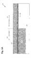
- FIG. 2Aillustrates a cross-sectional view, which includes a portion of a wafer processed according to an embodiment of the invention, corresponding to an initial step in the flowchart in FIG. 1 .
- FIG. 2Billustrates a cross-sectional view, which includes a portion of a wafer processed according to an embodiment of the invention, corresponding to an intermediate step in the flowchart in FIG. 1 .
- FIG. 2Cillustrates a cross-sectional view, which includes a portion of a wafer processed according to an embodiment of the invention, corresponding to an intermediate step in the flowchart in FIG. 1 .
- FIG. 2Dillustrates a cross-sectional view, which includes a portion of a wafer processed according to an embodiment of the invention, corresponding to an intermediate step in the flowchart in FIG. 1 .
- FIG. 2Eillustrates a cross-sectional view, which includes a portion of a wafer processed according to an embodiment of the invention, corresponding to a final step in the flowchart in FIG. 1 .
- FIG. 2Fillustrates a top view of a portion of the exemplary structure shown in FIG. 2E .
- the present inventionis directed to a method for forming a one-time programmable metal fuse and related structure.
- the following descriptioncontains specific information pertaining to the implementation of the present invention.
- One skilled in the artwill recognize that the present invention may be implemented in a manner different from that specifically discussed in the present application. Moreover, some of the specific details of the invention are not discussed in order not to obscure the invention.
- FIG. 1shows a flow chart illustrating a method according to an embodiment of the present invention. Certain details and features have been left out of flowchart 100 that are apparent to a person of ordinary skill in the art. For example, a step may consist of one or more substeps or may involve specialized equipment or materials, as known in the art. Steps 170 through 178 indicated in flowchart 100 are sufficient to describe one embodiment of the present invention; however, other embodiments of the invention may utilize steps different from those shown in flowchart 100 .
- processing steps shown in flowchart 100are performed on a portion of processed wafer, which, prior to step 170 , includes, among other things, a substrate, such as a silicon substrate, and an isolation region, such as a shallow trench isolation (STI) region, formed in the substrate.
- a substratesuch as a silicon substrate
- an isolation regionsuch as a shallow trench isolation (STI) region
- the waferis also referred to simply as a wafer or a semiconductor die or simply a die in the present application.
- structures 270 through 278 in FIGS. 2A through 2Eillustrate the result of performing steps 170 through 178 of flowchart 100 , respectively.
- structure 270shows a semiconductor structure after processing step 170
- structure 272shows structure 270 after the processing of step 172
- structure 274shows structure 272 after the processing of step 174 , and so forth.
- dielectric layer 202is formed over isolation region 204 in fuse region 205 of substrate 206 and over substrate 206 in transistor region 208 of substrate 206 , gate metal layer 210 is formed over dielectric layer 202 , and polycrystalline silicon (polysilicon) layer 212 is formed over gate metal layer 210 .
- Isolation region 204can be, for example, an STI region.
- Dielectric layer 202can comprise, for example, a dielectric material having a high dielectric constant (high-k), such as hafnium oxide (HfO), zirconium oxide (ZrO), or other type of metal oxide.
- dielectric layer 202can comprise a dielectric material other than a high-k dielectric material, such as, for example, silicon oxide. However, for process technologies below 32.0 nanometer (nm), dielectric layer 202 necessarily comprises a high-k dielectric material. Dielectric layer 202 can be formed by utilizing a chemical vapor deposition (CVD) process or other deposition process to deposit a layer of dielectric material over isolation region 204 and substrate 206 .
- CVDchemical vapor deposition
- Gate metal layer 210can comprise, for example, a metal stack including titanium nitride (TiN) or tantalum nitride (TaN), or other metallic material or metal stack that is suitable for use in a transistor gate.
- Metal layer 210can have a thickness of, for example, between approximately 30.0 Angstroms and approximately 200.0 Angstroms and can be formed over dielectric layer 202 be utilizing a physical vapor deposition (PVD) process or other deposition process.
- Polysilicon layer 212can comprise undoped polysilicon and can be formed by utilizing a low pressure chemical vapor deposition (LPCVD) process or other deposition process to deposit a layer of polysilicon over metal layer 210 .
- LPCVDlow pressure chemical vapor deposition
- one-time programmable metal fuse structure 214(also referred to simply as “metal fuse structure 214 ” in the present application) is formed over isolation region 204 and gate stack 216 is formed over substrate 206 .
- Metal fuse structure 214comprises dielectric segment 218 , which is situated over isolation region 204 , gate metal segment 220 , which is situated over dielectric segment 218 , and polysilicon segment 222 , which is situated over gate metal segment 220 .
- Gate metal segment 220includes gate metal fuse 223 , which is formed in a central portion of gate metal segment 220 .
- Gate metal fuse 223has thickness 225 , which can be, for example, between approximately 30.0 Angstroms and approximately 200.0 Angstroms. Gate metal fuse 223 has a width (not shown in FIG. 2B ) that can be, for example, approximately equal to a minimum width allowed by the process technology. The width of gate metal fuse 223 will be discussed below in relation to FIG. 2F .
- Gate stack 216comprises dielectric segment 224 , which is situated over substrate 206 , metal segment 226 , which is situated over dielectric segment 224 , and polysilicon segment 228 , which is situated over metal segment 226 .
- Metal fuse structure 214 and gate stack 216can be formed by appropriately patterning dielectric layer 202 , gate metal layer 210 , and polysilicon layer 212 in a patterning process, which can include appropriate masking and etching steps.
- the result of step 172 of flowchart 100is illustrated by structure 272 in FIG. 2B .
- doped polysilicon portions 230 and 232are formed in polysilicon segment 222 of metal fuse structure 214 and doped polysilicon segment 236 is formed in gate stack 216 .
- Undoped polysilicon portion 238is situated between doped polysilicon portions 230 and 232 of polysilicon segment 222 in metal fuse structure 214 and doped polysilicon segment 236 is situated over gate metal segment 226 of gate stack 216 .
- Undoped polysilicon portion 238also overlies gate metal fuse 223 in gate metal segment 220 .
- undoped polysilicon portion 238is substantially co-extensive with gate metal fuse 223 .
- Doped polysilicon portions 230 and 232 and doped polysilicon segment 236can be formed by, for example, forming a mask over substrate 206 and implanting an appropriate dopant into unmasked portions of polysilicon segment 222 and gate stack 216 .
- the dopantcan be an N type dopant.
- the dopantcan be a P type dopant.
- the maskcan be formed by depositing and appropriately patterning a layer of masking material, such as photoresist.
- spacers 242are formed adjacent to opposing sides of metal fuse structure 214 and spacers 244 are formed adjacent to opposing sides of gate stack 216 .
- Spacers 242 and 244can comprise a spacer dielectric material, such as, for example, silicon oxide, and can be formed in a manner known in the art.
- Source/drain regions(not shown in FIG. 2C ) can also be formed in substrate 206 adjacent to gate stack 216 at step 174 of flowchart 100 , thereby forming transistor 245 , which includes gate structure 216 .
- Transistor 245can be a field effect transistor (FET), such as a MOSFET.
- FETfield effect transistor
- silicide-blocking mask 246is formed over undoped polysilicon portion 238 of metal fuse structure 214 , silicide segments 248 and 250 are formed on respective doped polysilicon portions 230 and 232 of polysilicon segment 222 of metal fuse structure 214 , silicide segment 252 is formed on doped polysilicon segment 236 of gate stack 216 , and silicide segments 254 and 256 are formed on substrate 206 adjacent to gate stack 216 .
- Silicide-blocking mask 246is situated over undoped polysilicon portion 238 and overlaps doped polysilicon portions 230 and 232 so as to ensure that silicide is not formed on undoped polysilicon portion 238 .
- Silicide-blocking mask 246can comprise silicon nitride or other silicide-blocking material and can be formed by, for example, depositing and appropriately patterning a layer of silicon nitride over undoped polysilicon portion 238 of polysilicon segment 222 .
- silicide-blocking mask 246can be avoided by combining the formation of a silicide-blocking mask for fuse structure 214 with formation of a conventional silicide-blocking mask utilized in the formation of an unsalicided polysilicon resistor.
- Silicide segments 248 and 250are situated on respective doped polysilicon portions 230 and 232 of fuse structure 214
- silicide segment 252is situated on doped polysilicon segment 236 of gate stack 216
- silicide segments 254 and 256are situated on substrate 206 adjacent to spacers 244 .
- Silicide segments 248 and 250can extend above respective doped polysilicon portions 230 and 232 and can form respective terminals of metal fuse structure 214 .
- silicide segment 248can form a positive terminal (i.e. an anode) of metal fuse structure 214 and silicide segment 250 can form a negative terminal (i.e. a cathode) of metal fuse structure 214 .
- the result of step 176 of flowchart 100is illustrated by structure 276 in FIG. 2D .
- silicide-blocking mask 246(shown in FIG. 2D ) is removed from metal fuse structure 214 .
- Silicide-blocking mask 246can be removed by utilizing a suitable etch process as is known in the art.
- the result of step 178 of flowchart 100is illustrated by structure 278 in FIG. 2E .
- FIG. 2Fshows a top view of a portion of structure 278 , where the cross-sectional view of the portion of structure 278 in FIG. 2E is across line 2 E- 2 E in FIG. 2F .
- undoped polysilicon portions 230 and 232 , doped polysilicon portion 238 , and silicide segments 248 and 250correspond to the same elements in FIG. 2E and FIG. 2F .
- gate metal fuse 223which underlies undoped polysilicon portion 238 of polysilicon segment 222 , has width 258 . Width 258 can be, for example, approximately equal to a minimum width allowed by the process technology utilized to form metal fuse structure 214 and gate stack 216 .
- width 258can be approximately equal to 45.0 nm for a 45.0 nm process technology. approximately equal to 28.0 nm for a 28.0 nm process technology, and so forth.
- width 258 of gate metal fuse 223is not greater than approximately 40.0 nm. In another embodiment, width 258 of gate metal fuse 223 is not greater than approximately 32.0 nm.
- gate metal segment 220which includes gate metal fuse 223 , can have a resistance of, for example, approximately 10.0 ohms per square to approximately 100.0 ohms per square.
- undoped polysilicon portion 238 of polysilicon segment 222can have a substantially higher resistance of approximately 2000.0 ohms per square.
- Metal fuse structure 214can be programmed by causing a sufficient amount of current to flow between terminals 248 and 250 so as to cause gate metal fuse 223 to blow open. Thus, after programming, since gate metal fuse 223 is open, current flowing between terminals 248 and 250 of metal fuse structure 214 must flow through doped polysilicon portions 230 and 232 and undoped polysilicon portion 238 of polysilicon segment 218 , thereby causing metal fuse structure 214 to have a high resistance between terminals 248 and 250 .
- metal fuse structure 214prior to programming, i.e., before gate metal fuse 223 has been blown, current can flow between terminals 248 and 250 of metal fuse structure 214 via doped polysilicon portions 230 and 232 of polysilicon segment 222 and gate metal fuse 223 , thereby causing metal fuse structure 214 to have a low resistance between terminals 248 and 250 .
- the low resistance of metal fuse structure 214 prior to programmingcan be associated with a logic state of “0” and the high resistance of metal fuse structure 214 after programming can be associated with a logic state of “1”, or vice versa.
- the invention's gate metal fusecan have a very small width and thickness.
- an embodiment of the invention's gate metal fusecan have a width of less than approximately 40.0 nm and a thickness of less than approximately 20.0 nm.
- the invention's gate metal fusecan be fused (i.e. blown) in a programming operation by utilizing a very small current, which can be advantageously provided by a small-size FET.
- the invention's gate metal fusehas a very small size, less residue that can undesirably affect neighboring areas remains after the gate metal fuse has been fused (i.e. blown) in a programming operation.
- a conventional one-time programmable silicide fuse structure that is formed in a metal gate processcan require an additional mask to remove the gate metal that is utilized to form the metal gate, which can undesirably increase processing cost.
- a substantially higher programming currentcan be required to fuse the silicide compared to the programming current required to blow the gate metal in an embodiment of the invention's one-time programmable metal fuse structure.
- an embodiment of the inventioncan provide a one-time programmable metal fuse structure that can be advantageously programmed by utilizing a very small programming current, which can be advantageously provided by a small-size FET. Also, as discussed above, by utilizing a gate metal fuse, an embodiment of the invention can provide a one-time programmable metal fuse structure that can be formed in a high-k metal gate process for advanced process technologies, such as, for example, 32.0 nm or 28.0 nm process technologies, without requiring an additional mask, thereby advantageously reducing processing cost.
Landscapes
- Physics & Mathematics (AREA)
- Condensed Matter Physics & Semiconductors (AREA)
- General Physics & Mathematics (AREA)
- Engineering & Computer Science (AREA)
- Computer Hardware Design (AREA)
- Microelectronics & Electronic Packaging (AREA)
- Power Engineering (AREA)
- Design And Manufacture Of Integrated Circuits (AREA)
Abstract
Description
Claims (10)
Priority Applications (1)
| Application Number | Priority Date | Filing Date | Title |
|---|---|---|---|
| US13/466,986US8455977B2 (en) | 2009-06-22 | 2012-05-08 | Programmable fuse |
Applications Claiming Priority (2)
| Application Number | Priority Date | Filing Date | Title |
|---|---|---|---|
| US12/456,833US8178944B2 (en) | 2009-06-22 | 2009-06-22 | Method for forming a one-time programmable metal fuse and related structure |
| US13/466,986US8455977B2 (en) | 2009-06-22 | 2012-05-08 | Programmable fuse |
Related Parent Applications (1)
| Application Number | Title | Priority Date | Filing Date |
|---|---|---|---|
| US12/456,833DivisionUS8178944B2 (en) | 2009-06-22 | 2009-06-22 | Method for forming a one-time programmable metal fuse and related structure |
Publications (2)
| Publication Number | Publication Date |
|---|---|
| US20120217613A1 US20120217613A1 (en) | 2012-08-30 |
| US8455977B2true US8455977B2 (en) | 2013-06-04 |
Family
ID=43353529
Family Applications (2)
| Application Number | Title | Priority Date | Filing Date |
|---|---|---|---|
| US12/456,833Expired - Fee RelatedUS8178944B2 (en) | 2009-06-22 | 2009-06-22 | Method for forming a one-time programmable metal fuse and related structure |
| US13/466,986ActiveUS8455977B2 (en) | 2009-06-22 | 2012-05-08 | Programmable fuse |
Family Applications Before (1)
| Application Number | Title | Priority Date | Filing Date |
|---|---|---|---|
| US12/456,833Expired - Fee RelatedUS8178944B2 (en) | 2009-06-22 | 2009-06-22 | Method for forming a one-time programmable metal fuse and related structure |
Country Status (1)
| Country | Link |
|---|---|
| US (2) | US8178944B2 (en) |
Cited By (2)
| Publication number | Priority date | Publication date | Assignee | Title |
|---|---|---|---|---|
| US9754945B2 (en) | 2014-08-06 | 2017-09-05 | Globalfoundries Inc. | Non-volatile memory device employing a deep trench capacitor |
| CN109285974A (en)* | 2017-07-20 | 2019-01-29 | 宁德时代新能源科技股份有限公司 | Secondary cell top cap subassembly and secondary cell |
Families Citing this family (12)
| Publication number | Priority date | Publication date | Assignee | Title |
|---|---|---|---|---|
| US8071437B2 (en)* | 2009-11-19 | 2011-12-06 | United Microelectronics Corp. | Method of fabricating efuse, resistor and transistor |
| US20110198705A1 (en)* | 2010-02-18 | 2011-08-18 | Broadcom Corporation | Integrated resistor using gate metal for a resistive element |
| US8653623B2 (en)* | 2011-04-11 | 2014-02-18 | Taiwan Semiconductor Manufacturing Company, Ltd. | One-time programmable devices and methods of forming the same |
| US8841674B2 (en)* | 2011-06-30 | 2014-09-23 | Broadcom Corporaton | Field transistor structure manufactured using gate last process |
| US8493767B2 (en)* | 2011-10-04 | 2013-07-23 | Broadcom Corporation | One-time programmable device having an LDMOS structure |
| US9219059B2 (en) | 2012-09-26 | 2015-12-22 | International Business Machines Corporation | Semiconductor structure with integrated passive structures |
| US9093453B2 (en)* | 2013-10-07 | 2015-07-28 | International Business Machines Corporation | High performance e-fuse fabricated with sub-lithographic dimension |
| CN107785420B (en)* | 2016-08-29 | 2020-05-08 | 中芯国际集成电路制造(上海)有限公司 | Semiconductor device and method of manufacturing the same |
| US11456293B2 (en)* | 2019-08-23 | 2022-09-27 | Taiwan Semiconductor Manufacturing Co., Ltd. | Polysilicon resistor structures |
| CN116110878B (en)* | 2022-11-29 | 2024-11-08 | 芯合电子(上海)有限公司 | One-time programmable memory structure and preparation process thereof |
| US20240188287A1 (en)* | 2022-12-05 | 2024-06-06 | Globalfoundries U.S. Inc. | One-time programmable fuse using pn junction over gate metal layer, and related method |
| TWI841274B (en)* | 2023-03-03 | 2024-05-01 | 南亞科技股份有限公司 | Method of manufacturing semiconductor structure and fuse structure |
Citations (5)
| Publication number | Priority date | Publication date | Assignee | Title |
|---|---|---|---|---|
| US20080258256A1 (en)* | 2004-02-27 | 2008-10-23 | Nobuaki Otsuka | Semiconductor electrically programmable fuse element with amorphous silicon layer after programming and method of programming the same |
| US20080277756A1 (en)* | 2007-05-09 | 2008-11-13 | Freescale Semiconductor, Inc. | Electronic device and method for operating a memory circuit |
| US20100301417A1 (en)* | 2009-05-26 | 2010-12-02 | International Business Machines Corporation | Device including high-k metal gate finfet and resistive structure and method of forming thereof |
| US7943493B2 (en)* | 2007-10-26 | 2011-05-17 | International Business Machines Corporation | Electrical fuse having a fully silicided fuselink and enhanced flux divergence |
| US8004060B2 (en)* | 2007-11-29 | 2011-08-23 | International Business Machines Corporation | Metal gate compatible electrical antifuse |
Family Cites Families (1)
| Publication number | Priority date | Publication date | Assignee | Title |
|---|---|---|---|---|
| JP3565983B2 (en)* | 1996-04-12 | 2004-09-15 | 株式会社半導体エネルギー研究所 | Method for manufacturing semiconductor device |
- 2009
- 2009-06-22USUS12/456,833patent/US8178944B2/ennot_activeExpired - Fee Related
- 2012
- 2012-05-08USUS13/466,986patent/US8455977B2/enactiveActive
Patent Citations (5)
| Publication number | Priority date | Publication date | Assignee | Title |
|---|---|---|---|---|
| US20080258256A1 (en)* | 2004-02-27 | 2008-10-23 | Nobuaki Otsuka | Semiconductor electrically programmable fuse element with amorphous silicon layer after programming and method of programming the same |
| US20080277756A1 (en)* | 2007-05-09 | 2008-11-13 | Freescale Semiconductor, Inc. | Electronic device and method for operating a memory circuit |
| US7943493B2 (en)* | 2007-10-26 | 2011-05-17 | International Business Machines Corporation | Electrical fuse having a fully silicided fuselink and enhanced flux divergence |
| US8004060B2 (en)* | 2007-11-29 | 2011-08-23 | International Business Machines Corporation | Metal gate compatible electrical antifuse |
| US20100301417A1 (en)* | 2009-05-26 | 2010-12-02 | International Business Machines Corporation | Device including high-k metal gate finfet and resistive structure and method of forming thereof |
Cited By (4)
| Publication number | Priority date | Publication date | Assignee | Title |
|---|---|---|---|---|
| US9754945B2 (en) | 2014-08-06 | 2017-09-05 | Globalfoundries Inc. | Non-volatile memory device employing a deep trench capacitor |
| US10083967B2 (en) | 2014-08-06 | 2018-09-25 | Globalfoundries Inc. | Non-volatile memory device employing a deep trench capacitor |
| CN109285974A (en)* | 2017-07-20 | 2019-01-29 | 宁德时代新能源科技股份有限公司 | Secondary cell top cap subassembly and secondary cell |
| CN109285974B (en)* | 2017-07-20 | 2021-08-03 | 宁德时代新能源科技股份有限公司 | Secondary battery top cover assembly and secondary battery |
Also Published As
| Publication number | Publication date |
|---|---|
| US8178944B2 (en) | 2012-05-15 |
| US20100320561A1 (en) | 2010-12-23 |
| US20120217613A1 (en) | 2012-08-30 |
Similar Documents
| Publication | Publication Date | Title |
|---|---|---|
| US8455977B2 (en) | Programmable fuse | |
| US7176531B1 (en) | CMOS gates formed by integrating metals having different work functions and having a high-k gate dielectric | |
| CN100487911C (en) | Bimetallic grid transistor for CMOS process and manufacturing method thereof | |
| US8536006B2 (en) | Logic and non-volatile memory (NVM) integration | |
| US8409950B1 (en) | Method for integrating SONOS non-volatile memory into a sub-90 nm standard CMOS foundry process flow | |
| US8163640B2 (en) | Metal gate compatible electrical fuse | |
| US9536883B2 (en) | Dual anti-fuse | |
| US20090267130A1 (en) | Structure and process integration for flash storage element and dual conductor complementary mosfets | |
| US20140138777A1 (en) | Integrated circuit device and method for making same | |
| US9524962B2 (en) | Semiconductor device comprising an e-fuse and a FET | |
| US9129856B2 (en) | Method for efficiently fabricating memory cells with logic FETs and related structure | |
| CN101006568A (en) | Method of forming a nanocluster charge storage device | |
| US20170018557A1 (en) | Method for processing a carrier, a carrier, and a split gate field effect transistor structure | |
| US8766374B2 (en) | One-time programmable semiconductor device | |
| US20210384202A1 (en) | Semiconductor structure and method of forming the same | |
| US20090189280A1 (en) | Method of Forming a Non Volatile Memory Device | |
| CN106298676A (en) | Method for manufacturing semiconductor element | |
| US8822286B2 (en) | Method of fabricating a flash memory comprising a high-K dielectric and a metal gate | |
| US8241986B2 (en) | Semiconductor device and process for reducing damaging breakdown in gate dielectrics | |
| US8367494B2 (en) | Electrical fuse formed by replacement metal gate process | |
| US20090224324A1 (en) | Semiconductor device and manufacturing method thereof | |
| US9997518B2 (en) | Low resistive electrode for an extendable high-k metal gate stack | |
| US20080023765A1 (en) | Semiconductor Devices and Methods of Fabricating the Same | |
| US10276451B2 (en) | Semiconductor structure and method for forming the same | |
| US12068381B2 (en) | Transistor, ternary inverter including same, and transistor manufacturing method |
Legal Events
| Date | Code | Title | Description |
|---|---|---|---|
| AS | Assignment | Owner name:BROADCOM CORPORATION, CALIFORNIA Free format text:ASSIGNMENT OF ASSIGNORS INTEREST;ASSIGNORS:XIA, WEI;CHEN, XIANGDONG;ITO, AKIRA;REEL/FRAME:028176/0769 Effective date:20090529 | |
| STCF | Information on status: patent grant | Free format text:PATENTED CASE | |
| AS | Assignment | Owner name:BANK OF AMERICA, N.A., AS COLLATERAL AGENT, NORTH CAROLINA Free format text:PATENT SECURITY AGREEMENT;ASSIGNOR:BROADCOM CORPORATION;REEL/FRAME:037806/0001 Effective date:20160201 Owner name:BANK OF AMERICA, N.A., AS COLLATERAL AGENT, NORTH Free format text:PATENT SECURITY AGREEMENT;ASSIGNOR:BROADCOM CORPORATION;REEL/FRAME:037806/0001 Effective date:20160201 | |
| FPAY | Fee payment | Year of fee payment:4 | |
| AS | Assignment | Owner name:AVAGO TECHNOLOGIES GENERAL IP (SINGAPORE) PTE. LTD., SINGAPORE Free format text:ASSIGNMENT OF ASSIGNORS INTEREST;ASSIGNOR:BROADCOM CORPORATION;REEL/FRAME:041706/0001 Effective date:20170120 Owner name:AVAGO TECHNOLOGIES GENERAL IP (SINGAPORE) PTE. LTD Free format text:ASSIGNMENT OF ASSIGNORS INTEREST;ASSIGNOR:BROADCOM CORPORATION;REEL/FRAME:041706/0001 Effective date:20170120 | |
| AS | Assignment | Owner name:BROADCOM CORPORATION, CALIFORNIA Free format text:TERMINATION AND RELEASE OF SECURITY INTEREST IN PATENTS;ASSIGNOR:BANK OF AMERICA, N.A., AS COLLATERAL AGENT;REEL/FRAME:041712/0001 Effective date:20170119 | |
| AS | Assignment | Owner name:AVAGO TECHNOLOGIES INTERNATIONAL SALES PTE. LIMITE Free format text:MERGER;ASSIGNOR:AVAGO TECHNOLOGIES GENERAL IP (SINGAPORE) PTE. LTD.;REEL/FRAME:047230/0133 Effective date:20180509 | |
| AS | Assignment | Owner name:AVAGO TECHNOLOGIES INTERNATIONAL SALES PTE. LIMITE Free format text:CORRECTIVE ASSIGNMENT TO CORRECT THE EFFECTIVE DATE OF MERGER TO 09/05/2018 PREVIOUSLY RECORDED AT REEL: 047230 FRAME: 0133. ASSIGNOR(S) HEREBY CONFIRMS THE MERGER;ASSIGNOR:AVAGO TECHNOLOGIES GENERAL IP (SINGAPORE) PTE. LTD.;REEL/FRAME:047630/0456 Effective date:20180905 | |
| MAFP | Maintenance fee payment | Free format text:PAYMENT OF MAINTENANCE FEE, 8TH YEAR, LARGE ENTITY (ORIGINAL EVENT CODE: M1552); ENTITY STATUS OF PATENT OWNER: LARGE ENTITY Year of fee payment:8 | |
| MAFP | Maintenance fee payment | Free format text:PAYMENT OF MAINTENANCE FEE, 12TH YEAR, LARGE ENTITY (ORIGINAL EVENT CODE: M1553); ENTITY STATUS OF PATENT OWNER: LARGE ENTITY Year of fee payment:12 |