US8455936B2 - Configurable memory sheet and package assembly - Google Patents
Configurable memory sheet and package assemblyDownload PDFInfo
- Publication number
- US8455936B2 US8455936B2US12/712,554US71255410AUS8455936B2US 8455936 B2US8455936 B2US 8455936B2US 71255410 AUS71255410 AUS 71255410AUS 8455936 B2US8455936 B2US 8455936B2
- Authority
- US
- United States
- Prior art keywords
- memory
- asic
- sheet
- configurable
- memory sheet
- Prior art date
- Legal status (The legal status is an assumption and is not a legal conclusion. Google has not performed a legal analysis and makes no representation as to the accuracy of the status listed.)
- Active, expires
Links
- 230000015654memoryEffects0.000titleclaimsabstractdescription310
- 238000012360testing methodMethods0.000claimsdescription42
- 229910000679solderInorganic materials0.000claimsdescription41
- 238000000034methodMethods0.000claimsdescription40
- 230000008569processEffects0.000claimsdescription32
- 239000002184metalSubstances0.000claimsdescription21
- 229910052751metalInorganic materials0.000claimsdescription21
- 229910052710siliconInorganic materials0.000claimsdescription18
- 239000010703siliconSubstances0.000claimsdescription18
- XUIMIQQOPSSXEZ-UHFFFAOYSA-NSiliconChemical compound[Si]XUIMIQQOPSSXEZ-UHFFFAOYSA-N0.000claimsdescription13
- 239000000758substrateSubstances0.000claimsdescription12
- 238000009826distributionMethods0.000claimsdescription7
- 238000000059patterningMethods0.000claimsdescription6
- 238000005520cutting processMethods0.000claimsdescription5
- 230000000694effectsEffects0.000claimsdescription2
- 238000001816coolingMethods0.000claims1
- 238000004513sizingMethods0.000claims1
- 238000004519manufacturing processMethods0.000description13
- XEOCKQIQXJNTER-UHFFFAOYSA-Ngold palladium platinumChemical compound[Pd].[Pd].[Pd].[Pd].[Pd].[Pt].[Pt].[Pt].[Pt].[Pt].[Pt].[Au].[Au].[Au].[Au].[Au].[Au].[Au].[Au].[Au].[Au].[Au].[Au].[Au].[Au].[Au].[Au].[Au].[Au].[Au].[Au].[Au].[Au].[Au].[Au].[Au].[Au].[Au].[Au].[Au].[Au].[Au].[Au].[Au].[Au].[Au].[Au].[Au].[Au].[Au].[Au].[Au].[Au].[Au].[Au].[Au].[Au].[Au].[Au].[Au].[Au].[Au].[Au].[Au].[Au].[Au].[Au].[Au].[Au].[Au].[Au].[Au].[Au].[Au].[Au].[Au].[Au].[Au].[Au].[Au].[Au].[Au].[Au].[Au].[Au].[Au].[Au].[Au].[Au].[Au].[Au].[Au].[Au].[Au].[Au].[Au].[Au].[Au]XEOCKQIQXJNTER-UHFFFAOYSA-N0.000description11
- 238000010586diagramMethods0.000description10
- 239000000523sampleSubstances0.000description10
- 238000013461designMethods0.000description8
- 238000005516engineering processMethods0.000description8
- 230000004927fusionEffects0.000description7
- 229910052802copperInorganic materials0.000description5
- 239000010949copperSubstances0.000description5
- 238000012545processingMethods0.000description5
- 230000006870functionEffects0.000description4
- 230000003071parasitic effectEffects0.000description4
- RYGMFSIKBFXOCR-UHFFFAOYSA-NCopperChemical compound[Cu]RYGMFSIKBFXOCR-UHFFFAOYSA-N0.000description3
- 230000008901benefitEffects0.000description3
- 239000003990capacitorSubstances0.000description3
- 238000001459lithographyMethods0.000description3
- 239000000463materialSubstances0.000description3
- 239000004065semiconductorSubstances0.000description3
- 238000012546transferMethods0.000description3
- VYPSYNLAJGMNEJ-UHFFFAOYSA-NSilicium dioxideChemical compoundO=[Si]=OVYPSYNLAJGMNEJ-UHFFFAOYSA-N0.000description2
- BOTDANWDWHJENH-UHFFFAOYSA-NTetraethyl orthosilicateChemical compoundCCO[Si](OCC)(OCC)OCCBOTDANWDWHJENH-UHFFFAOYSA-N0.000description2
- 239000004020conductorSubstances0.000description2
- 239000012212insulatorSubstances0.000description2
- 230000010354integrationEffects0.000description2
- 230000006855networkingEffects0.000description2
- 238000000638solvent extractionMethods0.000description2
- 230000003466anti-cipated effectEffects0.000description1
- 238000003491arrayMethods0.000description1
- 230000000903blocking effectEffects0.000description1
- 238000004891communicationMethods0.000description1
- 230000000295complement effectEffects0.000description1
- 238000007906compressionMethods0.000description1
- 230000008878couplingEffects0.000description1
- 238000010168coupling processMethods0.000description1
- 238000005859coupling reactionMethods0.000description1
- 238000005336crackingMethods0.000description1
- 229910003460diamondInorganic materials0.000description1
- 239000010432diamondSubstances0.000description1
- 239000012467final productSubstances0.000description1
- 230000017525heat dissipationEffects0.000description1
- 230000003993interactionEffects0.000description1
- 230000013011matingEffects0.000description1
- 229910044991metal oxideInorganic materials0.000description1
- 150000004706metal oxidesChemical class0.000description1
- 230000008520organizationEffects0.000description1
- 238000002161passivationMethods0.000description1
- 238000012805post-processingMethods0.000description1
- 239000002243precursorSubstances0.000description1
- 238000004886process controlMethods0.000description1
- 238000011165process developmentMethods0.000description1
- 230000008439repair processEffects0.000description1
- 235000012239silicon dioxideNutrition0.000description1
- 239000000377silicon dioxideSubstances0.000description1
- 239000007787solidSubstances0.000description1
Images


Classifications
- H—ELECTRICITY
- H10—SEMICONDUCTOR DEVICES; ELECTRIC SOLID-STATE DEVICES NOT OTHERWISE PROVIDED FOR
- H10D—INORGANIC ELECTRIC SEMICONDUCTOR DEVICES
- H10D89/00—Aspects of integrated devices not covered by groups H10D84/00 - H10D88/00
- H10D89/10—Integrated device layouts
- G—PHYSICS
- G11—INFORMATION STORAGE
- G11C—STATIC STORES
- G11C29/00—Checking stores for correct operation ; Subsequent repair; Testing stores during standby or offline operation
- G11C29/04—Detection or location of defective memory elements, e.g. cell constructio details, timing of test signals
- G11C29/08—Functional testing, e.g. testing during refresh, power-on self testing [POST] or distributed testing
- G11C29/12—Built-in arrangements for testing, e.g. built-in self testing [BIST] or interconnection details
- G11C29/1201—Built-in arrangements for testing, e.g. built-in self testing [BIST] or interconnection details comprising I/O circuitry
- G—PHYSICS
- G11—INFORMATION STORAGE
- G11C—STATIC STORES
- G11C29/00—Checking stores for correct operation ; Subsequent repair; Testing stores during standby or offline operation
- G11C29/04—Detection or location of defective memory elements, e.g. cell constructio details, timing of test signals
- G11C29/08—Functional testing, e.g. testing during refresh, power-on self testing [POST] or distributed testing
- G11C29/48—Arrangements in static stores specially adapted for testing by means external to the store, e.g. using direct memory access [DMA] or using auxiliary access paths
- H—ELECTRICITY
- H01—ELECTRIC ELEMENTS
- H01L—SEMICONDUCTOR DEVICES NOT COVERED BY CLASS H10
- H01L21/00—Processes or apparatus adapted for the manufacture or treatment of semiconductor or solid state devices or of parts thereof
- H01L21/70—Manufacture or treatment of devices consisting of a plurality of solid state components formed in or on a common substrate or of parts thereof; Manufacture of integrated circuit devices or of parts thereof
- H01L21/71—Manufacture of specific parts of devices defined in group H01L21/70
- H01L21/768—Applying interconnections to be used for carrying current between separate components within a device comprising conductors and dielectrics
- H01L21/76898—Applying interconnections to be used for carrying current between separate components within a device comprising conductors and dielectrics formed through a semiconductor substrate
- H—ELECTRICITY
- H01—ELECTRIC ELEMENTS
- H01L—SEMICONDUCTOR DEVICES NOT COVERED BY CLASS H10
- H01L23/00—Details of semiconductor or other solid state devices
- H01L23/48—Arrangements for conducting electric current to or from the solid state body in operation, e.g. leads, terminal arrangements ; Selection of materials therefor
- H01L23/481—Internal lead connections, e.g. via connections, feedthrough structures
- H—ELECTRICITY
- H03—ELECTRONIC CIRCUITRY
- H03K—PULSE TECHNIQUE
- H03K19/00—Logic circuits, i.e. having at least two inputs acting on one output; Inverting circuits
- H03K19/02—Logic circuits, i.e. having at least two inputs acting on one output; Inverting circuits using specified components
- H03K19/173—Logic circuits, i.e. having at least two inputs acting on one output; Inverting circuits using specified components using elementary logic circuits as components
- H03K19/177—Logic circuits, i.e. having at least two inputs acting on one output; Inverting circuits using specified components using elementary logic circuits as components arranged in matrix form
- H03K19/17748—Structural details of configuration resources
- H03K19/1776—Structural details of configuration resources for memories
- H—ELECTRICITY
- H03—ELECTRONIC CIRCUITRY
- H03K—PULSE TECHNIQUE
- H03K19/00—Logic circuits, i.e. having at least two inputs acting on one output; Inverting circuits
- H03K19/02—Logic circuits, i.e. having at least two inputs acting on one output; Inverting circuits using specified components
- H03K19/173—Logic circuits, i.e. having at least two inputs acting on one output; Inverting circuits using specified components using elementary logic circuits as components
- H03K19/177—Logic circuits, i.e. having at least two inputs acting on one output; Inverting circuits using specified components using elementary logic circuits as components arranged in matrix form
- H03K19/1778—Structural details for adapting physical parameters
- H03K19/17796—Structural details for adapting physical parameters for physical disposition of blocks
- H—ELECTRICITY
- H10—SEMICONDUCTOR DEVICES; ELECTRIC SOLID-STATE DEVICES NOT OTHERWISE PROVIDED FOR
- H10B—ELECTRONIC MEMORY DEVICES
- H10B12/00—Dynamic random access memory [DRAM] devices
- H10B12/01—Manufacture or treatment
- H10B12/09—Manufacture or treatment with simultaneous manufacture of the peripheral circuit region and memory cells
- H—ELECTRICITY
- H10—SEMICONDUCTOR DEVICES; ELECTRIC SOLID-STATE DEVICES NOT OTHERWISE PROVIDED FOR
- H10B—ELECTRONIC MEMORY DEVICES
- H10B12/00—Dynamic random access memory [DRAM] devices
- H10B12/50—Peripheral circuit region structures
- H—ELECTRICITY
- H10—SEMICONDUCTOR DEVICES; ELECTRIC SOLID-STATE DEVICES NOT OTHERWISE PROVIDED FOR
- H10D—INORGANIC ELECTRIC SEMICONDUCTOR DEVICES
- H10D84/00—Integrated devices formed in or on semiconductor substrates that comprise only semiconducting layers, e.g. on Si wafers or on GaAs-on-Si wafers
- H10D84/90—Masterslice integrated circuits
- H10D84/998—Input and output buffer/driver structures
- G—PHYSICS
- G11—INFORMATION STORAGE
- G11C—STATIC STORES
- G11C29/00—Checking stores for correct operation ; Subsequent repair; Testing stores during standby or offline operation
- G11C29/04—Detection or location of defective memory elements, e.g. cell constructio details, timing of test signals
- G11C2029/0401—Detection or location of defective memory elements, e.g. cell constructio details, timing of test signals in embedded memories
- H—ELECTRICITY
- H01—ELECTRIC ELEMENTS
- H01L—SEMICONDUCTOR DEVICES NOT COVERED BY CLASS H10
- H01L2224/00—Indexing scheme for arrangements for connecting or disconnecting semiconductor or solid-state bodies and methods related thereto as covered by H01L24/00
- H01L2224/73—Means for bonding being of different types provided for in two or more of groups H01L2224/10, H01L2224/18, H01L2224/26, H01L2224/34, H01L2224/42, H01L2224/50, H01L2224/63, H01L2224/71
- H01L2224/732—Location after the connecting process
- H01L2224/73201—Location after the connecting process on the same surface
- H01L2224/73203—Bump and layer connectors
- H01L2224/73204—Bump and layer connectors the bump connector being embedded into the layer connector
- H—ELECTRICITY
- H01—ELECTRIC ELEMENTS
- H01L—SEMICONDUCTOR DEVICES NOT COVERED BY CLASS H10
- H01L23/00—Details of semiconductor or other solid state devices
- H01L23/52—Arrangements for conducting electric current within the device in operation from one component to another, i.e. interconnections, e.g. wires, lead frames
- H01L23/522—Arrangements for conducting electric current within the device in operation from one component to another, i.e. interconnections, e.g. wires, lead frames including external interconnections consisting of a multilayer structure of conductive and insulating layers inseparably formed on the semiconductor body
- H01L23/525—Arrangements for conducting electric current within the device in operation from one component to another, i.e. interconnections, e.g. wires, lead frames including external interconnections consisting of a multilayer structure of conductive and insulating layers inseparably formed on the semiconductor body with adaptable interconnections
- H—ELECTRICITY
- H01—ELECTRIC ELEMENTS
- H01L—SEMICONDUCTOR DEVICES NOT COVERED BY CLASS H10
- H01L23/00—Details of semiconductor or other solid state devices
- H01L23/52—Arrangements for conducting electric current within the device in operation from one component to another, i.e. interconnections, e.g. wires, lead frames
- H01L23/522—Arrangements for conducting electric current within the device in operation from one component to another, i.e. interconnections, e.g. wires, lead frames including external interconnections consisting of a multilayer structure of conductive and insulating layers inseparably formed on the semiconductor body
- H01L23/528—Layout of the interconnection structure
- H01L23/5286—Arrangements of power or ground buses
- H—ELECTRICITY
- H01—ELECTRIC ELEMENTS
- H01L—SEMICONDUCTOR DEVICES NOT COVERED BY CLASS H10
- H01L2924/00—Indexing scheme for arrangements or methods for connecting or disconnecting semiconductor or solid-state bodies as covered by H01L24/00
- H01L2924/10—Details of semiconductor or other solid state devices to be connected
- H01L2924/102—Material of the semiconductor or solid state bodies
- H01L2924/1025—Semiconducting materials
- H01L2924/10251—Elemental semiconductors, i.e. Group IV
- H01L2924/10253—Silicon [Si]
- Y—GENERAL TAGGING OF NEW TECHNOLOGICAL DEVELOPMENTS; GENERAL TAGGING OF CROSS-SECTIONAL TECHNOLOGIES SPANNING OVER SEVERAL SECTIONS OF THE IPC; TECHNICAL SUBJECTS COVERED BY FORMER USPC CROSS-REFERENCE ART COLLECTIONS [XRACs] AND DIGESTS
- Y10—TECHNICAL SUBJECTS COVERED BY FORMER USPC
- Y10T—TECHNICAL SUBJECTS COVERED BY FORMER US CLASSIFICATION
- Y10T29/00—Metal working
- Y10T29/49—Method of mechanical manufacture
- Y10T29/49002—Electrical device making
- Y10T29/49117—Conductor or circuit manufacturing
- Y10T29/49124—On flat or curved insulated base, e.g., printed circuit, etc.
- Y10T29/4913—Assembling to base an electrical component, e.g., capacitor, etc.
Definitions
- a modern application specific integrated circuitrequires a significant amount of random access memory (RAM) to operate satisfactorily.
- RAMrandom access memory
- the memoryneeds to be accessed at a high rate with low latency.
- a single ASIC chipneeds to read and write independently to multiple memory elements.
- DRAMdynamic RAM
- eDRAMembedded DRAM
- eDRAM memoryis dense and, being on the same chip with the ASIC logic, allows dense, high-speed interconnections between the memory and the logic.
- eDRAMalso avoids the slow, narrow, power-hungry interface entailed in connecting a logic die to separate DRAM dice through either packages and a printed circuit board (PCB) or in a side-by-side multi-chip module (MCM).
- PCBprinted circuit board
- MCMside-by-side multi-chip module
- Embedded DRAMhowever presents a number of challenges.
- the additional processing steps to embed the memory with the logicadds cost and reduces yield.
- the embedded DRAMis not as dense as it is in a dedicated DRAM and it is less stable.
- a stacked-capacitordeepens the first contact to a point at which it significantly increases its resistance and capacitance thus lowering the performance of the logic.
- embedded DRAM technologyis not widely available.
- TSVfine pitch through-silicon via
- TSSthrough-silicon stacking
- An area array interconnect using TSVs and metal-to-metal bondsprovide physically short, low parasitic connections, to provide what can be referred to as “I/O-less on-chip access to off-chip technology.”
- I/O-less on-chip access to off-chip technologySuch through-silicon stacking allows the consideration of partitioning an IC device into separate logic and DRAM dice.
- Advantages of through-silicon stacking of logic and DRAM over connecting them together on a PCB or MCMinclude, for example, lower power consumption and higher speed due to dramatically lower interconnect parasitics, interface simplification, wider, denser interface permitting higher data transfer rate and greater architectural flexibility, and less printed circuit board (PCB) area, which can also be a disadvantage with regard to heat removal.
- PCBprinted circuit board
- a configurable memory sheetincludes a plurality of segmentable memory banks arranged on a repeating grid such that the plurality of segmentable memory banks can be configured for applications with a variety of circuit elements, where the plurality of segmentable memory banks are configured into memories by their connections to the variety of circuit elements.
- FIG. 1is a schematic diagram illustrating a portion of an embodiment of a configurable memory sheet.
- FIG. 2is a schematic diagram illustrating a DRAM bank of FIG. 1 .
- FIG. 3is a schematic diagram illustrating a cross-sectional view of an integrated package assembly in which an application specific integrated circuit is oriented in a face to face configuration with a portion of the configurable memory sheet.
- FIG. 4is a schematic diagram illustrating a configurable memory sheet configured to have active memory and inactive memory.
- FIG. 5is a schematic diagram illustrating a cross-sectional view of a portion of the package assembly of FIG. 3 showing stacked semiconductor dice.
- FIG. 6is a flow chart illustrating the fabrication of an embodiment of the configurable memory sheet of FIG. 1 and the package assembly of FIG. 3 .
- a configurable memory sheetallows simple integration of DRAM with a variety of different ASICs.
- a configurable memory sheetis fabricated using repeating DRAM banks.
- the repeating DRAM banksare partitioned into chips based on the configuration of the ASIC device with which the DRAM will be used.
- the repeating DRAM banksare integrated with an area array of contacts.
- the array of contactscan be arranged on a predetermined grid spacing, depending on the fabrication process used to fabricate the DRAM.
- a solder bump arraycan be used to connect the DRAM banks to the package substrate using solder bumps arranged on a 150 micrometer ( ⁇ m) grid. Other grid spacing is contemplated.
- the contacts on the predetermined grid spacingcan also accommodate through silicon vias (TSVs).
- TSVscan be formed through the configurable memory sheet and implemented to deliver power from a package substrate to the configurable memory sheet and also through the configurable memory sheet to an ASIC device located adjacent the configurable memory sheet.
- the configurability of the memory sheetstems from the ability to customize the connections between the memory banks on the configurable memory sheet and the ASIC by the arrangement of the ASIC's circuit blocks and the routing of the ASIC's connections to the configurable memory sheet, as well as by using a front side redistribution layer (RDL) to provide connection between the configurable memory sheet and the ASIC.
- RDLredistribution layer
- the front side RDLallows a relatively simple and inexpensive processing step to customize the connections between the configurable memory sheet and the ASIC. In this manner, the use of separate processes to fabricate the memory and the ASIC allow each to be separately and independently optimized and a single memory sheet design can be used with multiple ASIC designs.
- the configurability of the memory sheetalso stems from the ability to customize the power and signal connections between the configurable memory sheet and the solder bump array by using a back side redistribution layer (RDL).
- RDLback side redistribution layer
- the back side RDLallows a relatively simple and inexpensive processing step to customize the connections between the configurable memory sheet and the solder bump array on the package substrate.
- the configurable memory sheetgenerally uses a smaller portion of the total number of available solder bumps for power and ground than does the ASIC, the configurable memory sheet also allows access points for testing circuit elements on the memory.
- an ASIC die and the die formed using portions of the configurable memory sheetare arranged in a face-to-face configuration.
- Such an arrangementallows a heatsink to be attached to a rear surface of the ASIC for heat dissipation.
- the two dice in the stackhave approximately the same dimensions because high power ASICs generally need a fully populated solder bump array to uniformly supply electrical power and because the thermal conductivity of silicon maximizes the transfer of heat from the bottom die (e.g., the DRAM) through the top die (e.g., the ASIC) to the heatsink by materials with matched coefficients of thermal expansion (CTE).
- CTEcoefficients of thermal expansion
- the ASIC at the top of the stackis oriented face down with its rear surface to the heatsink for a number of reasons.
- finer pitch connectionscan be made between the dice by bonding pads face-to-face as opposed to bonding back-to-front with through-silicon vias.
- face-to-face stacking with approximately equal die sizesuses TSVs to supply signals and power using the solder bump array on the grid spacing defined herein.
- the DRAMSince the density of the external power and signal connections is less than the anticipated density of ASIC logic to DRAM connection, and since it is easier to address the signal routing issue in a regular structure, it is simpler to put the DRAM on the bottom and design it to accommodate the TSVs. This also places all the non-standard processing into one die—the DRAM, which, being a standard wafer, can share its design and process development effort over an entire family of ASICs.
- CMOScomplementary metal oxide semiconductor
- solder bumps on the back of the diea stronger, better-adhering material such as silicon dioxide formed using a tetraethyl orthosilicate precursor (TEOS) can be used to insulate the solder bumps from the silicon substrate. Since the backside metal is coarse, its insulator can be made thick to reduce capacitance.
- TEOStetraethyl orthosilicate precursor
- FIG. 1is a schematic diagram illustrating a portion of an embodiment of a configurable memory sheet 100 .
- the configurable memory sheet 100can be thought of as a “pseudochip” representing a unit in which repeating instances of the configurable memory sheet 100 are photolithographically exposed during wafer fabrication and probed during wafer test.
- the configurable memory sheet 100is fabricated using a process that is optimized for use in fabricating dynamic random access memory (DRAM).
- the DRAMcan be fabricated using a trench-capacitor process, a stacked-capacitor process, or any other DRAM fabrication process known to those skilled in the art.
- Each configurable memory sheet 100is constructed from a number of different layers, including, for example, a substrate layer, such as silicon, one or more layers that include the active memory elements and one or more layers that include connections within the configurable memory sheet.
- the configurable memory sheet 100includes a number of pads 124 .
- the pads 124are laid out on a grid, which in this example, is a grid having a pitch of 150 micrometers ( ⁇ m) ⁇ 150 ⁇ m.
- a connection structure referred to as a through silicon via (TSV) 126can be associated with some or all of the pads 124 .
- TSVs 126can be formed in the configurable memory sheet 100 over the entire array of pads 124 , but need not occupy every pad location.
- the configurable memory sheet 100also comprises an array of unconnected DRAM banks 102 dispersed throughout the regular (150 ⁇ m ⁇ 150 ⁇ m) solder bump array, which is designed primarily as a power distribution network for delivering power to the DRAM banks 102 and to a circuit (for example, an ASIC, but not shown in FIG. 1 ) that is mated to the configurable memory sheet 100 .
- Some pads 124particularly those under the ASIC die perimeter, carry input/output signals instead of power.
- the 150 ⁇ m dimensionis not particularly significant. Any regular grid dimension can be implemented such that a DRAM bank 102 fits between solder bumps at their minimum pitch.
- the configurable memory sheet 100includes DRAM banks 102 a , 102 b , 102 c and 102 d . It should be mentioned that although four DRAM banks 102 are shown, a typical configurable memory sheet 100 will have many hundreds or even many thousands of such DRAM banks 102 .
- Each DRAM bank 102comprises a complete memory containing memory cells, row and column decoders, sense amplifiers, and repair resources. Since the DRAM does not need power to be delivered on the full TSV grid, frontside probe pads can be connected to all the TSVs used to power the final stack and some of these can be used to probe DRAM test signals.
- the center four pads 142 , 144 , 146 and 148 of the DRAM bank 102 acould also function as a traditional scan test access port (TAP) for the signals Test Mode Select (TMS), Test Data Input (TDI), Test Data Output (TDO), and Test Clock (TCK).
- TAPTest Mode Select
- TDITest Data Input
- TDOTest Data Output
- TCKTest Clock
- a number of DRAM banks 102 and associated design-for-test (DfT) structures 134 and process monitor structures 128can be thought of as a pseudochip that contains all repeated patterns below the customization levels (to be described below) that can easily fit on a stepper reticle and that can be tested in a single probe touchdown.
- the pseudochipfits in one exposure field so that no patterns are stitched across exposure fields. In this manner, it is possible to test many DRAM banks 102 simultaneously.
- programmable built-in self-test (BIST) engines and process monitorscan be distributed over the process monitor/test spaces of the many DRAM banks of a pseudochip and a wide test port can be distributed over the DRAM banks. Since the BIST engine is built in the DRAM process while its test connections and pads are created in the redistribution layer (RDL) post-process, the differences in repeat intervals are accommodated by the RDL routing, which is accomplished by full-wafer lithography.
- RDLredistribution layer
- the configurable memory sheet 100includes a number of memory subarrays.
- the DRAM bank 102 aincludes memory subarrays 104 and 106 ;
- the DRAM bank 102 bincludes memory subarrays 108 and 112 ;
- the DRAM bank 102 cincludes memory subarrays 114 and 116 ;
- the DRAM bank 102 dincludes memory sub arrays 118 and 122 . While two memory subarrays are illustrated in FIG. 1 for each DRAM bank 102 , each DRAM bank 102 may comprise additional memory subarrays.
- each memory subarraycan include a particular memory configuration.
- each memory subarray shown in FIG. 1can be fabricated to include a 16K ⁇ 36 RAM structure. However, other memory structures are possible.
- Each DRAM bank 102is integrated with a grid of four (4) by three (3) pads 124 .
- each pad 124is designed to correspond to an electrical and/or mechanical connection.
- the pads 124can be designed to accommodate a solder connection, referred to as a solder bump, a metal-to-metal fusion bond, or another electrical and mechanical connection, such that electrical contact can be made to elements within the configurable memory sheet 100 .
- the pads 124can be designed to accept any other type of connection, as will be described below.
- the pads 124are designed to provide power (i.e., supply and ground signals), and test signal access.
- each TSV 126can be formed to extend through layers of the configurable memory sheet 100 to provide electrical connectivity through the configurable memory sheet 100 to a logic element located over the configurable memory sheet 100 , and to provide electrical connectivity to elements within the configurable memory sheet 100 .
- the configurable memory sheet 100has no circuit routing traces in the near vicinity of a TSV. Accordingly, what is referred to as a “TSV-last” process can be used to form the TSVs.
- TSV-last processeliminates the requirement that the foundry that fabricates the configurable memory sheet 100 also fabricates the TSVs.
- the TSV-last processallows the configurable memory sheet 100 to be fabricated to a general specification and it allows all of the memory sheet customization to be performed in a post-processing manner.
- An example assembly processbonds known-good ASIC dice to known-good DRAM sites, and then singulates the DRAM wafer and assembles the ASIC/DRAM stacks into packages.
- the configurable memory sheet 100is configured into a die to match the memory structure, die size, and power and input/output (I/O) solder bump configuration of the ASIC to which it will be mated. As will be described below, configuration is done primarily in a front side redistribution metal layer (RDL) and associated pad and contact layers.
- RDLredistribution metal layer
- the TSVsmay also be configured to the ASIC. All of these configurable layers are fabricated using inexpensive masks and processes after the configurable memory sheet 100 is fabricated using conventional DRAM processing. Further, prior to integrating the configurable memory sheet 100 with an additional circuit die, such as an ASIC, the configurable memory sheet 100 can be wafer tested by probing the pads 124 that will later deliver power to the ASIC.
- the configurable memory sheet 100also includes a number of process monitors 128 and 132 .
- the process monitors 128 and 132are generally formed in predetermined locations on the configurable memory sheet 100 , and are used to monitor the fabrication process when the configurable memory sheet 100 is being fabricated.
- the configurable memory sheet 100also includes design for test (DfT) blocks 134 and 136 .
- the DfT blocks 134 and 136serve as conduits for the application of test signals from test probes (not shown) to the memory circuit elements within the configurable memory sheet 100 being tested. Further, the DfT blocks 134 and 136 may also serve to generate and evaluate test patterns.
- the configurable memory sheet 100is designed to be segmented, or divided, into sections that correspond to the logic element (in this example, an application specific integrated circuit (ASIC)) with which the configurable memory sheet is being integrated.
- ASICapplication specific integrated circuit
- an ASICcan be vertically integrated over sectioned portions of the configurable memory sheet 100 such that the two elements form a vertically integrated package having a similar footprint.
- the configurable memory sheet 100is designed to be sectioned along the dotted lines shown in FIG. 1 such that 450 ⁇ m ⁇ 300 ⁇ m portions of the configurable memory sheet 100 can be formed, depending on the memory needs and the physical requirements of the ASIC to which the configurable memory sheet 100 will be paired. In an embodiment, many hundreds of sections of DRAM banks 102 will be formed for any particular ASIC application. The integration of the configurable memory sheet 100 and an application-specific integrated circuit will be described in further detail below.
- FIG. 2is a schematic diagram illustrating a DRAM bank 102 a of FIG. 1 .
- the DRAM bank 102 aincludes subarray 104 and subarray 106 .
- the number of subarrays in a DRAM bank 102is arbitrary, and generally driven by design factors.
- the DRAM bank 102 ais a memory cell array.
- the DRAM bank 102 ais split into two subarrays, 104 , 106 , to provide for the middle row of four TSVs, 232 , 234 , 236 and 238 . Since a subarray is a solid, regular structure, it can't be punctured by a TSV and probe pad.
- the DRAM bank(comprising two subarrays in the example herein) uses a certain number of small interdie signal pads, also referred to herein as micropads, or micro-bond pads 202 , to achieve the desired data transfer rate.
- micropadssmall interdie signal pads
- the subarrays 104 and 106are illustrated having micro-bond pads 202 to indicate electrical contact from the memory elements within the subarrays 104 and 106 to the top surface of the subarrays 104 and 106 .
- the DfT block 134is shown as providing test access to the subarray 104 and to the subarray 106 .
- the pads 124 and the TSVs 126are illustrated in larger scale, but on the same example 150 ⁇ m pitch as shown in FIG. 1 .
- the subarray 104 and the subarray 106share the 12 pads 124 after the DRAM bank 102 a has been sectioned as described above with respect to FIG. 1 .
- a fully functioning DRAM bank 102 ais created from the configurable memory sheet 100 .
- any number of fully functioning DRAM banks 102can be formed from the configurable memory sheet 100 ( FIG. 1 ), depending on the logic element to which the DRAM will be mated.
- the steps used to configure the configurable memory sheet 100 into dice for a specific ASICshould to be performed using coarse lithography and inexpensive masks.
- the mask fieldshould encompass at least one DRAM bank, but process monitors 128 and DfT blocks 134 ( 136 , FIG. 1 ), may benefit from a larger field, i.e. a pseudochip of multiple banks.
- Thiscan be accomplished using a full-wafer (300 mm) 1:1 proximity exposure by a mask aligner such as the IQ mask aligner available from the EV Group, Phoenix Ariz., or another suitable mask aligner available from, for example, Canon Corporation. This minimizes restrictions on repeating lithography features across the wafer such as might be desired to temporarily share test resources during wafer probe.
- a stepping projection alignersuch as one available from Ultratech, Inc.
- the DfT block 134 and process monitors 128should be made to fit the stepper's limited field size. Using a stepper should avoid circuit stitching issues because the exposure field can be sized to abut at DRAM die boundaries that will be cut at singulation.
- the configurable memory sheet 100comprises small, repeating units.
- the configurable memory sheet 100comprises many, small, wide (72-bit word) DRAM banks 102 .
- the configurable memory sheet 100is mated with an ASIC that is fabricated using a 40 nanometer (nm) process that includes a 150 ⁇ m solder bump pitch to distribute power.
- using a 58 nm DRAM fabrication processprovides a cell size of 0.0202 ⁇ m 2 with an area efficiency of 56%.
- Conservatively reducing the efficiency to 50% to account for the small DRAM bank size, and using a 72-bit wide DRAM bank 102results in the ability to fit 21 of the 25 ⁇ m pitch micro-bond pads 202 in the 150 ⁇ m square area 210 between pads 124 , thus using six such squares to accommodate the I/O of a DRAM bank 102 .
- the configurable memory sheet 100includes DRAM banks 102 , which occupy an area of 2 ⁇ 3 pads 124 (300 ⁇ m ⁇ 450 ⁇ m) with a data organization of 72 k ⁇ 16 k for a capacity of 1.18 Mb. This provides 512 Mb capacity to cover a large ASIC.
- the die containing the configurable memory sheet 100is singulated.
- Singulationis the process of separating the wafer into individual chips. Singulation can be performed by cutting with a diamond saw. However, to reduce damage around the cut lines sometimes the cutting is initiated by a laser through the metal and dielectric layers and then finished with a saw through the silicon. In some applications, a deep etch is used to separate the chips. In conventional integrated circuits the cut lines are devoid of circuitry. However, in the example configurable memory sheet described herein, the cuts are made through inactive memory elements so as to save the substantial space that would be occupied by incorporating an unpopulated cut line (also known as a scribe street or saw kerf) into each repeated memory bank.
- an unpopulated cut linealso known as a scribe street or saw kerf
- the unused DRAM bankscan be deactivated and isolated from the active DRAM banks by patterning the front RDL so that damage to the unused DRAM banks does not electrically affect the final product.
- the pads 124 and respective TSVs 126 that supply power and groundare labeled “P” and “G” respectively, in FIG. 2 .
- the pads 124can be used to not only supply power (power and ground) but also to provide test access.
- the center four pads 242 , 244 , 246 and 248could also function as a traditional scan test access port (TAP) for the signals TMS, TDI, TDO, and TCK.
- TAPscan test access port
- the pad 242can provide ground (G) and access to the TMS test signal; the pad 244 can provide power (P) and access to the TDI test signal; the pad 246 could provide power (P) and access to the TDO test signal; and the pad 238 could provide power (P) and access to the TCK test signal.
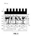
- FIG. 3is a schematic diagram illustrating a cross-sectional view of an integrated package assembly 300 , including stacked semiconductor dice, in which an application specific integrated circuit is oriented in a face to face configuration with a portion of the configurable memory sheet 100 .
- the package assembly 300includes a package substrate 302 over which a connection layer 304 is formed.
- the connection layer 304comprises solder bumps 306 , 308 and 312 that form a solder bump array, as described above.
- An underfill material 307occupies the space between the solder bumps 306 , 308 and 312 .
- the solder bumps 306 , 308 and 312correspond to the pads 124 shown in FIGS. 1 and 2 .
- FIG. 3Although a small portion of the circuitry is shown in FIG. 3 , it is to be understood that there can be many hundreds or thousands of such solder bump connections in an actual package assembly.
- the package substrate 302provides connection for the package assembly to a printed circuit board (PCB) a printed wiring board (PWB) or other assembly on which the package assembly 300 is ultimately installed.
- PCBprinted circuit board
- PWBprinted wiring board
- a back side redistribution metal layer (RDL) 314is formed over a surface of the memory sheet 332 to provide connection to the connection layer 304 .
- the backside RDL 314includes a backside dielectric layer 318 against which a backside passivation layer 316 is formed.
- the backside dielectric layer 318comprises a strong dielectric to isolate and insulate the solder bumps from the rear surface of the memory sheet 332 , thereby alleviating effects of die-to-package thermal expansion mismatch
- the backside RDL 314also includes circuit traces 322 , 324 and 326 .
- the circuit traces 322 , 324 and 326provide electrical connection from respective solder bumps 306 , 308 and 312 , to the memory sheet 332 .
- the memory sheet 332illustrates a section of the configurable memory sheet 100 after the memory sheet is sectioned.
- the memory sheet 332can also be referred to as the DRAM die.
- the memory sheet 332includes a silicon layer 334 and a die interconnect stack layer 336 , through which are formed TSVs 338 , 342 and 344 , respectively.
- the TSVs 338 , 342 and 344are formed using a TSV-last process as described above and as known to those skilled in the art.
- the TSVscan be formed using a TSV-middle process, as also known to those skilled in the art.
- the die interconnect stack 336includes examples of circuitry located in the memory sheet 332 .
- the circuitry 346 and 348are merely two examples of active memory elements that can be contained in the memory sheet 332 . Many additional circuitry elements can be part of the memory sheet 332 .
- the memory sheet 332also includes electrical connectivity elements located through the die interconnect stack 336 as shown by exemplary circuit traces 352 and 354 .
- the die interconnect stack 336includes many other circuit elements and circuit interconnect elements.
- the die interconnect stack 336is the layer in which the active memory elements, such as memory element 346 and memory element 348 , are shown at the transistor device level.
- through silicon viasare formed so as to extend completely through the memory sheet 332 , on the same grid pattern as are the solder bumps 306 , 308 and 312 .
- a front side redistribution metal layer (RDL) 362is formed over the memory sheet 332 .
- the front side RDL 362provides electrical connectivity from the memory sheet 332 to the ASIC 372 , and allows the memory sheet 332 to be generically formed as the configurable memory sheet 100 shown in FIGS. 1 and 2 . In this manner, the configurable memory sheet 100 can be fabricated in a process optimized for DRAM fabrication and then customized to any of a number of logic elements (such as the ASIC 372 ) using the front side RDL 362 .
- the front side RDL 362includes exemplary probe, interdie and bonding pads 364 , 366 and 384 , respectively.
- the front side RDL 362also includes exemplary conductive traces 391 , 392 and 393 , which form the electrical paths of the redistribution layer, and includes exemplary contact layer portions 394 , 395 and 396 , which fill the holes that make contact to the top metal layer of the memory sheet 332 .
- there are many additional pads, conductive traces and contact layer portions within the front side RDL 362so that signals can be connected from the ASIC 372 to the memory sheet 332 .
- the pads 364 , 366 and 384 , the circuit traces 391 , 392 and 393 and the contact layer portions 394 , 395 and 396can be formed using copper, or another electrically conductive material.
- the pad 384includes a corresponding pad 386 located within the ASIC 372 .
- An exemplary technique to attach the ASIC 372 to the front side RDL 362can include copper-to-copper fusion bonding along the line 368 between the pads on the upper surface of the front side RDL 362 and the pads on the facing surface of the ASIC 372 .
- the pads 384 and 386are implemented as what is referred to as interdie fusion pads, and the ASIC 372 is electrically coupled to the memory sheet 332 using a fine-pitch area array interdie interconnect.
- Copper-to-copper fusion bondingoccurs when copper surfaces are brought together at room temperature after being polished smooth and chemically activated. The bond is made permanent by a low-temperature (e.g. 125° C.) anneal under light pressure.
- fusion micro solder bumpscan be used at a temperature of around 300° C. to provide the bond, or possibly thermo-compression bonding can be used at approximately 400° C.
- Fusion bond padscan be on the order of 10 ⁇ m ⁇ 10 ⁇ m on a 25 ⁇ m pitch with die-to-die alignment of 1 ⁇ m or better. Micro solder bumps are coarser—on the order of 40 ⁇ m pitch. All of these connection methods usually dedicate a layer of metal to bonding pads.
- the repeating memory bank structureis designed so that all of its connections to the TSVs it encloses and all interdie pads (micropads) are made by the front side RDL 362 .
- the front side RDL 362is customized to each mating ASIC design. Since all power is carried by the TSVs, not patterning connections between the power TSVs and a memory bank isolates the memory bank from power. Similarly, since all memory address, data, and control signals are carried between the ASIC 372 and a memory bank by micropads, not patterning these pads in the front side RDL 362 on a particular bank disconnects these signals from the memory bank.
- the configurable memory sheet 100includes active memory banks and inactive memory banks.
- the inactive memory banksare deactivated and isolated from the active memory banks by patterning the front side RDL 362 .
- the memory bankswere rendered inactive by cutting through them to singulate the memory sheet this is done so that damage to the separated inactive memory banks does not electrically affect the active memory banks.
- isolating themsaves power and lessens noise coupling into active circuits.
- the ASIC 372which can also be referred to as the ASIC die, includes exemplary circuit elements 374 , 376 and 378 .
- the ASIC 372also includes exemplary conductive traces 382 and 386 . Although unnumbered for simplicity, the ASIC 372 includes many additional active circuit elements and electrical conductors.
- a heat sink 392is coupled to the ASIC 372 using a thermal interface 388 .
- the ASIC 372will generate significantly more heat than will the memory sheet 332 .
- the heat generated by the ASIC 372is transferred directly through the thermal interface 388 to the heatsink 392 .
- Heat generated by the memory sheet 332will be transferred to the ASIC 372 along the TSVs and across the interface 368 .
- mounting the memory sheet 332 and the ASIC 372 in a face-to-face orientation as shown in FIG. 3simplifies the connections to the package substrate 302 and also allows the TSVs 338 , 342 and 344 to provide a fully populated power grid to deliver power to the memory sheet 332 and to the ASIC 372 .
- External signals and powerare communicated to the package substrate 302 using the TSVs.
- connections between the die (the die having the configurable memory sheet 332 and the die having the ASIC 372 ) and the package 302are made by wire bonds or solder bumps to pads on the face of the die. Since the die having the configurable memory sheet 332 and the die having the ASIC 372 are bonded face-to-face and are of the same size, neither face is exposed. Therefore the signals and power from the shared face are routed using the TSVs through the bottom die (the die having the configurable memory sheet 332 ) to the package 302 . Further, locating a solder bump (e.g., 306 ) at an end of a TSV (e.g., 338 ) produces less capacitance and resistance than running a length of backside RDL from the TSV to a bump.
- a solder bumpe.g., 306
- the TSVsare arrayed directly on top of their corresponding solder bumps and the DRAM circuitry and interdie fusion pads are fit between them as shown in FIG. 3 .
- the CTE mismatch between the silicon die and the copper that fills the TSVcreates a strain field surrounding the TSV. This strain affects transistor performance (primarily mobility) so FETs are excluded from a radius of approximately 2-3 TSV radii from the TSV center.
- FIG. 4is a schematic diagram illustrating a configurable memory sheet 400 configured to have active memory 401 and inactive memory 403 .
- the inactive memory 403can be located adjacent to ASIC elements that do not necessarily require the use of active memory 401 .
- the configurable memory sheet 400includes DRAM banks 402 a , 402 b , 402 c and 402 d .
- the DRAM bank 402 aincludes subarrays 404 and 406 .
- the DRAM bank 402 bincludes subarrays 408 and 412 .
- the subarrays 404 , 406 , 408 and 412are fabricated without micro-bond pads 202 ( FIG. 2 ) because no memory connections thereto are required for the inactive memory 403 .
- the DRAM bank 402 cincludes subarrays 414 and 416 and the DRAM bank 402 d includes subarrays 418 and 422 .
- the DRAM banks 402 c and 402 dare implemented as active memory as described above, and therefore include micro-bond pads 435 to connect ASIC circuitry (not shown) to active memory elements.
- the micro-bond pads 435are similar to the micro-bond pads 202 described above.
- the assignment of the TSVs and the use of the DRAM banks 402depends on the particular requirements and functionality of the ASIC circuit to which they mate. Under core ASIC circuitry the TSVs only provide power so they alternate between power and ground in such a way that abutting DRAM banks 402 can share solder bumps. For example, the DRAM bank 402 c shares power TSV 462 and ground TSV 464 with DRAM bank 402 d.
- Memory banks 402 c and 402 drepresent active memory banks so that the TSVs on their boundary (i.e., TSVs 462 , 464 , 468 and 472 ) describe how the TSV power and ground pattern matches on memory bank abutment.
- the memory banks 402 a and 402 billustrate unused memory.
- the memory bank 402 aillustrates an unused memory bank that is instead used to provide input and output (I/O signals to an ASIC through an unused memory bank.
- I/O signalsinput and output signals to an ASIC through an unused memory bank.
- the ASICcontains a differential serialized/deserializer (SERDES)
- SERDESdifferential serialized/deserializer
- the TSV 426can be used to carry the RX+ signal
- the TSV 476can be used to carry the TX+ signal
- the TSV 478can be used to carry the RX ⁇ signal
- the TSV 482can be used to carry the TX ⁇ signal.
- Other TSVs in the unused memory bank 402 acan be used to carry, for example, one or more power supply signals for the I/O functions.
- the elementsi.e., pads, connected TSVs and solder bumps
- the elementsthat would otherwise be part of the power distribution network are reassigned by the design of the front side RDL 362 to signals entering or exiting the stacked chips that comprise the package assembly 300 . This is accomplished by disconnecting (making inactive) the memory banks (e.g., 402 a in FIG. 4 ) in which they are located. This feature of selectively re-assigning pads from power to I/O allows the configurable memory sheet 100 work in high power applications.
- the memory bank 402 bis illustrated as a completely unconnected memory bank, and as such, carries no signals.
- the memory sheet 332receives power from these TSVs as connected by the front side RDL 362 ( FIG. 3 ). If the memory sheet 362 uses different power supplies than the ASIC 372 ( FIG. 3 ) then the TSVs are assigned to power supplies in a more complicated pattern and the front side RDL 362 is connected accordingly. Since DRAM memory sheet 332 consumes significantly less power than does the ASIC 372 , the DRAM memory sheet 332 does not require power and ground to be supplied by every P and G pair of TSVs. The memory sheet 332 under the ASIC core (the active memory 401 ) is used as needed by the ASIC 372 .
- Memory banks 402 that are not usedcan be disconnected from power by not connecting them to power or ground TSVs with the front side RDL 362 .
- micro-bond padsneed not be formed on unused memory banks or on the ASIC area adjacent to them since there are no interdie signals there, as shown by inactive memory 403 .
- DRAM bank 402When a DRAM bank 402 lies beneath an ASIC I/O, as in the DRAM banks 402 a and 402 b on the left side of FIG. 4 , which can be located at the perimeter of the ASIC 372 , most of the ASICs TSVs are dedicated to I/O signals and supplies so the DRAM bank is not useable, and is made inactive so as to not couple noise into the ASIC I/O signal paths. The unused DRAM bank 402 is completely disconnected.
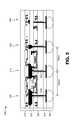
- FIG. 5is a schematic diagram illustrating a cross-sectional view 500 of a portion of the package assembly 300 of FIG. 3 .
- FIG. 5illustrates four combinations of TSVs and pads that can be fabricated using the configurable memory sheet 100 .
- the combination shown at 510includes power being supplied to the ASIC 572 and to the memory sheet 532 and includes probeable pads on both the ASIC die and on the memory die for wafer test prior to bonding, power delivery to the stack and easy bonding.
- the combination shown using reference numeral 510includes a probeable pad 515 that provides a power feed to the memory sheet 532 and to the ASIC 572 where the relatively large pad size simplifies bonding.
- the combination shown using reference numeral 520includes a probeable test signal pad 525 that allows test access to the memory sheet 532 before bonding to the ASIC and a power feed to the ASIC 572 where the relatively large probe pad simplifies bonding. After bonding, the combination of the TSV 535 and pad 525 is used exclusively to power the ASIC 572 , while the DRAM 532 permanently switches off its test signal connection to this pad stack.
- the combination 510connects to power supply wires in the memory bank while the combination 520 connects to memory test signals in the memory sheet 532 .
- reference numeral 530illustrates a high-speed input-output path using micropads on both the ASIC die and the DRAM die to reduce capacitance. These pads are too small to be probed for test.
- the combination shown using reference numeral 540shows a solder bump and TSV completely disconnected front side RDL 562 , which shows no connection between the memory sheet 532 and the ASIC 572 .
- the DRAM sheet 572does not need power to be delivered on this fine a grid, and since capacitance generally helps the power system, front side probe pads can be connected to all the TSVs used to power the final package assembly 500 and some of these can be used to probe DRAM test signals.
- the center four pads 242 , 244 , 246 and 248 ( FIG. 2 ) of a DRAM bank 102 a ( FIG. 2 )could double as a traditional scan test access port for the signals TMS, TDI, TDO, and TCK. After bonding, multiplexers could then reconnect this TAP to micropads for testing of the package assembly and the TSVs 232 , 234 , 236 and 238 then used to power the ASIC 572 .
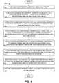
- FIG. 6is a flow chart 600 illustrating the fabrication of an embodiment of the configurable memory sheet of FIG. 1 and the package assembly of FIG. 3 . Although shown in a particular order, the blocks in the flow chart can be performed in or out of the order shown, and in certain embodiments, can be performed in parallel.
- a configurable memory sheetis formed by fabricating a plurality of segmentable memory banks on a repeating grid using a dedicated DRAM fabrication process.
- the segmentable memory banksare configured for applications with a variety of circuit elements by adapting connections between the segmentable memory banks and a particular circuit element with which the segmentable memory banks will be mated.
- a front side RDLis formed on the configurable memory sheet to electrically couple active memory elements in the segmentable memory banks to circuitry on an ASIC.
- padsare formed on the configurable memory sheet such that each of the pads is associated with a corresponding location in a power distribution network. At least a portion of the pads are power pads that deliver electrical power to the configurable memory sheet and to the ASIC.
- a portion of the pads (and connected TSVs and solder bumps) that otherwise would be part of the power distribution networkare assigned to signals entering or exiting the integrated package assembly 300 and disconnecting, thereby making inactive, the memory banks in which this portion of the pads are located.
- a TSVis formed in the configurable memory sheet at each location that includes a pad.
- Each TSVforms a substantially vertical connection between a location on the ASIC and a corresponding solder bump located on a rear surface of the configurable memory sheet.
- a portion of the power padsare used to test the configurable memory sheet before integrating the configurable memory sheet with the (ASIC).
- the configurable memory sheetis sized to closely match the dimensions of the ASIC.
Landscapes
- Physics & Mathematics (AREA)
- Engineering & Computer Science (AREA)
- Mathematical Physics (AREA)
- Computer Hardware Design (AREA)
- Computing Systems (AREA)
- General Engineering & Computer Science (AREA)
- Condensed Matter Physics & Semiconductors (AREA)
- General Physics & Mathematics (AREA)
- Microelectronics & Electronic Packaging (AREA)
- Power Engineering (AREA)
- Manufacturing & Machinery (AREA)
- Semiconductor Memories (AREA)
Abstract
Description
Claims (21)
Priority Applications (1)
| Application Number | Priority Date | Filing Date | Title |
|---|---|---|---|
| US12/712,554US8455936B2 (en) | 2010-02-25 | 2010-02-25 | Configurable memory sheet and package assembly |
Applications Claiming Priority (1)
| Application Number | Priority Date | Filing Date | Title |
|---|---|---|---|
| US12/712,554US8455936B2 (en) | 2010-02-25 | 2010-02-25 | Configurable memory sheet and package assembly |
Publications (2)
| Publication Number | Publication Date |
|---|---|
| US20110204917A1 US20110204917A1 (en) | 2011-08-25 |
| US8455936B2true US8455936B2 (en) | 2013-06-04 |
Family
ID=44475995
Family Applications (1)
| Application Number | Title | Priority Date | Filing Date |
|---|---|---|---|
| US12/712,554Active2031-11-19US8455936B2 (en) | 2010-02-25 | 2010-02-25 | Configurable memory sheet and package assembly |
Country Status (1)
| Country | Link |
|---|---|
| US (1) | US8455936B2 (en) |
Cited By (6)
| Publication number | Priority date | Publication date | Assignee | Title |
|---|---|---|---|---|
| US20140264827A1 (en)* | 2013-03-12 | 2014-09-18 | Anna M. Prakash | Methods of forming wafer level underfill materials and structures formed thereby |
| WO2015003553A1 (en)* | 2013-07-10 | 2015-01-15 | 格科微电子(上海)有限公司 | Dynamic random access memory (dram) and production method, semiconductor packaging component and packaging method |
| EP3096350A1 (en)* | 2015-05-21 | 2016-11-23 | MediaTek Inc. | Semiconductor package assembly and method for forming the same |
| TWI618159B (en)* | 2015-05-21 | 2018-03-11 | 聯發科技股份有限公司 | Semiconductor package assembly and methods for forming the same |
| US20240079318A1 (en)* | 2022-09-06 | 2024-03-07 | Western Digital Technologies, Inc. | Nand die with rdl for altered bond wire bandwidth in memory devices |
| TWI840812B (en)* | 2021-09-16 | 2024-05-01 | 日商鎧俠股份有限公司 | Semiconductor storage device with bonding electrodes |
Families Citing this family (170)
| Publication number | Priority date | Publication date | Assignee | Title |
|---|---|---|---|---|
| US11018133B2 (en) | 2009-10-12 | 2021-05-25 | Monolithic 3D Inc. | 3D integrated circuit |
| US10388863B2 (en) | 2009-10-12 | 2019-08-20 | Monolithic 3D Inc. | 3D memory device and structure |
| US10366970B2 (en) | 2009-10-12 | 2019-07-30 | Monolithic 3D Inc. | 3D semiconductor device and structure |
| US12027518B1 (en) | 2009-10-12 | 2024-07-02 | Monolithic 3D Inc. | 3D semiconductor devices and structures with metal layers |
| US10910364B2 (en) | 2009-10-12 | 2021-02-02 | Monolitaic 3D Inc. | 3D semiconductor device |
| US11374118B2 (en) | 2009-10-12 | 2022-06-28 | Monolithic 3D Inc. | Method to form a 3D integrated circuit |
| US11984445B2 (en) | 2009-10-12 | 2024-05-14 | Monolithic 3D Inc. | 3D semiconductor devices and structures with metal layers |
| US12362219B2 (en) | 2010-11-18 | 2025-07-15 | Monolithic 3D Inc. | 3D semiconductor memory device and structure |
| US11482440B2 (en) | 2010-12-16 | 2022-10-25 | Monolithic 3D Inc. | 3D semiconductor device and structure with a built-in test circuit for repairing faulty circuits |
| US10497713B2 (en) | 2010-11-18 | 2019-12-03 | Monolithic 3D Inc. | 3D semiconductor memory device and structure |
| US11018191B1 (en) | 2010-10-11 | 2021-05-25 | Monolithic 3D Inc. | 3D semiconductor device and structure |
| US11600667B1 (en) | 2010-10-11 | 2023-03-07 | Monolithic 3D Inc. | Method to produce 3D semiconductor devices and structures with memory |
| US11469271B2 (en) | 2010-10-11 | 2022-10-11 | Monolithic 3D Inc. | Method to produce 3D semiconductor devices and structures with memory |
| US11257867B1 (en) | 2010-10-11 | 2022-02-22 | Monolithic 3D Inc. | 3D semiconductor device and structure with oxide bonds |
| US11024673B1 (en) | 2010-10-11 | 2021-06-01 | Monolithic 3D Inc. | 3D semiconductor device and structure |
| US10896931B1 (en) | 2010-10-11 | 2021-01-19 | Monolithic 3D Inc. | 3D semiconductor device and structure |
| US11315980B1 (en) | 2010-10-11 | 2022-04-26 | Monolithic 3D Inc. | 3D semiconductor device and structure with transistors |
| US11158674B2 (en) | 2010-10-11 | 2021-10-26 | Monolithic 3D Inc. | Method to produce a 3D semiconductor device and structure |
| US11227897B2 (en) | 2010-10-11 | 2022-01-18 | Monolithic 3D Inc. | Method for producing a 3D semiconductor memory device and structure |
| US11869915B2 (en) | 2010-10-13 | 2024-01-09 | Monolithic 3D Inc. | Multilevel semiconductor device and structure with image sensors and wafer bonding |
| US11163112B2 (en) | 2010-10-13 | 2021-11-02 | Monolithic 3D Inc. | Multilevel semiconductor device and structure with electromagnetic modulators |
| US10833108B2 (en) | 2010-10-13 | 2020-11-10 | Monolithic 3D Inc. | 3D microdisplay device and structure |
| US12360310B2 (en) | 2010-10-13 | 2025-07-15 | Monolithic 3D Inc. | Multilevel semiconductor device and structure with oxide bonding |
| US11437368B2 (en) | 2010-10-13 | 2022-09-06 | Monolithic 3D Inc. | Multilevel semiconductor device and structure with oxide bonding |
| US11043523B1 (en) | 2010-10-13 | 2021-06-22 | Monolithic 3D Inc. | Multilevel semiconductor device and structure with image sensors |
| US11164898B2 (en) | 2010-10-13 | 2021-11-02 | Monolithic 3D Inc. | Multilevel semiconductor device and structure |
| US11929372B2 (en) | 2010-10-13 | 2024-03-12 | Monolithic 3D Inc. | Multilevel semiconductor device and structure with image sensors and wafer bonding |
| US11133344B2 (en) | 2010-10-13 | 2021-09-28 | Monolithic 3D Inc. | Multilevel semiconductor device and structure with image sensors |
| US11855114B2 (en) | 2010-10-13 | 2023-12-26 | Monolithic 3D Inc. | Multilevel semiconductor device and structure with image sensors and wafer bonding |
| US11984438B2 (en) | 2010-10-13 | 2024-05-14 | Monolithic 3D Inc. | Multilevel semiconductor device and structure with oxide bonding |
| US11694922B2 (en) | 2010-10-13 | 2023-07-04 | Monolithic 3D Inc. | Multilevel semiconductor device and structure with oxide bonding |
| US11404466B2 (en) | 2010-10-13 | 2022-08-02 | Monolithic 3D Inc. | Multilevel semiconductor device and structure with image sensors |
| US11855100B2 (en) | 2010-10-13 | 2023-12-26 | Monolithic 3D Inc. | Multilevel semiconductor device and structure with oxide bonding |
| US11063071B1 (en) | 2010-10-13 | 2021-07-13 | Monolithic 3D Inc. | Multilevel semiconductor device and structure with waveguides |
| US12080743B2 (en) | 2010-10-13 | 2024-09-03 | Monolithic 3D Inc. | Multilevel semiconductor device and structure with image sensors and wafer bonding |
| US10943934B2 (en) | 2010-10-13 | 2021-03-09 | Monolithic 3D Inc. | Multilevel semiconductor device and structure |
| US11327227B2 (en) | 2010-10-13 | 2022-05-10 | Monolithic 3D Inc. | Multilevel semiconductor device and structure with electromagnetic modulators |
| US10679977B2 (en) | 2010-10-13 | 2020-06-09 | Monolithic 3D Inc. | 3D microdisplay device and structure |
| US11605663B2 (en) | 2010-10-13 | 2023-03-14 | Monolithic 3D Inc. | Multilevel semiconductor device and structure with image sensors and wafer bonding |
| US10978501B1 (en) | 2010-10-13 | 2021-04-13 | Monolithic 3D Inc. | Multilevel semiconductor device and structure with waveguides |
| US10998374B1 (en) | 2010-10-13 | 2021-05-04 | Monolithic 3D Inc. | Multilevel semiconductor device and structure |
| US12094892B2 (en) | 2010-10-13 | 2024-09-17 | Monolithic 3D Inc. | 3D micro display device and structure |
| US11521888B2 (en) | 2010-11-18 | 2022-12-06 | Monolithic 3D Inc. | 3D semiconductor device and structure with high-k metal gate transistors |
| US11784082B2 (en) | 2010-11-18 | 2023-10-10 | Monolithic 3D Inc. | 3D semiconductor device and structure with bonding |
| US11443971B2 (en) | 2010-11-18 | 2022-09-13 | Monolithic 3D Inc. | 3D semiconductor device and structure with memory |
| US11482439B2 (en) | 2010-11-18 | 2022-10-25 | Monolithic 3D Inc. | Methods for producing a 3D semiconductor memory device comprising charge trap junction-less transistors |
| US11495484B2 (en) | 2010-11-18 | 2022-11-08 | Monolithic 3D Inc. | 3D semiconductor devices and structures with at least two single-crystal layers |
| US12033884B2 (en) | 2010-11-18 | 2024-07-09 | Monolithic 3D Inc. | Methods for producing a 3D semiconductor device and structure with memory cells and multiple metal layers |
| US11569117B2 (en) | 2010-11-18 | 2023-01-31 | Monolithic 3D Inc. | 3D semiconductor device and structure with single-crystal layers |
| US11735462B2 (en) | 2010-11-18 | 2023-08-22 | Monolithic 3D Inc. | 3D semiconductor device and structure with single-crystal layers |
| US12068187B2 (en) | 2010-11-18 | 2024-08-20 | Monolithic 3D Inc. | 3D semiconductor device and structure with bonding and DRAM memory cells |
| US11508605B2 (en) | 2010-11-18 | 2022-11-22 | Monolithic 3D Inc. | 3D semiconductor memory device and structure |
| US11610802B2 (en) | 2010-11-18 | 2023-03-21 | Monolithic 3D Inc. | Method for producing a 3D semiconductor device and structure with single crystal transistors and metal gate electrodes |
| US11923230B1 (en) | 2010-11-18 | 2024-03-05 | Monolithic 3D Inc. | 3D semiconductor device and structure with bonding |
| US11094576B1 (en) | 2010-11-18 | 2021-08-17 | Monolithic 3D Inc. | Methods for producing a 3D semiconductor memory device and structure |
| US12100611B2 (en) | 2010-11-18 | 2024-09-24 | Monolithic 3D Inc. | Methods for producing a 3D semiconductor device and structure with memory cells and multiple metal layers |
| US11862503B2 (en) | 2010-11-18 | 2024-01-02 | Monolithic 3D Inc. | Method for producing a 3D semiconductor device and structure with memory cells and multiple metal layers |
| US11004719B1 (en) | 2010-11-18 | 2021-05-11 | Monolithic 3D Inc. | Methods for producing a 3D semiconductor memory device and structure |
| US11615977B2 (en) | 2010-11-18 | 2023-03-28 | Monolithic 3D Inc. | 3D semiconductor memory device and structure |
| US11854857B1 (en) | 2010-11-18 | 2023-12-26 | Monolithic 3D Inc. | Methods for producing a 3D semiconductor device and structure with memory cells and multiple metal layers |
| US11107721B2 (en) | 2010-11-18 | 2021-08-31 | Monolithic 3D Inc. | 3D semiconductor device and structure with NAND logic |
| US11804396B2 (en) | 2010-11-18 | 2023-10-31 | Monolithic 3D Inc. | Methods for producing a 3D semiconductor device and structure with memory cells and multiple metal layers |
| US12243765B2 (en) | 2010-11-18 | 2025-03-04 | Monolithic 3D Inc. | 3D semiconductor device and structure with metal layers and memory cells |
| US12154817B1 (en) | 2010-11-18 | 2024-11-26 | Monolithic 3D Inc. | Methods for producing a 3D semiconductor memory device and structure |
| US12136562B2 (en) | 2010-11-18 | 2024-11-05 | Monolithic 3D Inc. | 3D semiconductor device and structure with single-crystal layers |
| US11355381B2 (en) | 2010-11-18 | 2022-06-07 | Monolithic 3D Inc. | 3D semiconductor memory device and structure |
| US11482438B2 (en) | 2010-11-18 | 2022-10-25 | Monolithic 3D Inc. | Methods for producing a 3D semiconductor memory device and structure |
| US11018042B1 (en) | 2010-11-18 | 2021-05-25 | Monolithic 3D Inc. | 3D semiconductor memory device and structure |
| US11355380B2 (en) | 2010-11-18 | 2022-06-07 | Monolithic 3D Inc. | Methods for producing 3D semiconductor memory device and structure utilizing alignment marks |
| US11121021B2 (en) | 2010-11-18 | 2021-09-14 | Monolithic 3D Inc. | 3D semiconductor device and structure |
| US12272586B2 (en) | 2010-11-18 | 2025-04-08 | Monolithic 3D Inc. | 3D semiconductor memory device and structure with memory and metal layers |
| US12144190B2 (en) | 2010-11-18 | 2024-11-12 | Monolithic 3D Inc. | 3D semiconductor device and structure with bonding and memory cells preliminary class |
| US11031275B2 (en) | 2010-11-18 | 2021-06-08 | Monolithic 3D Inc. | 3D semiconductor device and structure with memory |
| US12125737B1 (en) | 2010-11-18 | 2024-10-22 | Monolithic 3D Inc. | 3D semiconductor device and structure with metal layers and memory cells |
| US11901210B2 (en) | 2010-11-18 | 2024-02-13 | Monolithic 3D Inc. | 3D semiconductor device and structure with memory |
| US11164770B1 (en) | 2010-11-18 | 2021-11-02 | Monolithic 3D Inc. | Method for producing a 3D semiconductor memory device and structure |
| US11211279B2 (en)* | 2010-11-18 | 2021-12-28 | Monolithic 3D Inc. | Method for processing a 3D integrated circuit and structure |
| US8916910B2 (en)* | 2010-12-13 | 2014-12-23 | Research Foundation Of State University Of New York | Reconfigurable RF/digital hybrid 3D interconnect |
| US11735501B1 (en) | 2012-04-09 | 2023-08-22 | Monolithic 3D Inc. | 3D semiconductor device and structure with metal layers and a connective path |
| US11410912B2 (en) | 2012-04-09 | 2022-08-09 | Monolithic 3D Inc. | 3D semiconductor device with vias and isolation layers |
| US11164811B2 (en) | 2012-04-09 | 2021-11-02 | Monolithic 3D Inc. | 3D semiconductor device with isolation layers and oxide-to-oxide bonding |
| US11616004B1 (en) | 2012-04-09 | 2023-03-28 | Monolithic 3D Inc. | 3D semiconductor device and structure with metal layers and a connective path |
| US11881443B2 (en) | 2012-04-09 | 2024-01-23 | Monolithic 3D Inc. | 3D semiconductor device and structure with metal layers and a connective path |
| US11594473B2 (en) | 2012-04-09 | 2023-02-28 | Monolithic 3D Inc. | 3D semiconductor device and structure with metal layers and a connective path |
| US11088050B2 (en) | 2012-04-09 | 2021-08-10 | Monolithic 3D Inc. | 3D semiconductor device with isolation layers |
| US10600888B2 (en) | 2012-04-09 | 2020-03-24 | Monolithic 3D Inc. | 3D semiconductor device |
| US11694944B1 (en) | 2012-04-09 | 2023-07-04 | Monolithic 3D Inc. | 3D semiconductor device and structure with metal layers and a connective path |
| US11476181B1 (en) | 2012-04-09 | 2022-10-18 | Monolithic 3D Inc. | 3D semiconductor device and structure with metal layers |
| US9646899B2 (en)* | 2012-09-13 | 2017-05-09 | Micron Technology, Inc. | Interconnect assemblies with probed bond pads |
| US11018116B2 (en) | 2012-12-22 | 2021-05-25 | Monolithic 3D Inc. | Method to form a 3D semiconductor device and structure |
| US11916045B2 (en) | 2012-12-22 | 2024-02-27 | Monolithic 3D Inc. | 3D semiconductor device and structure with metal layers |
| US11784169B2 (en) | 2012-12-22 | 2023-10-10 | Monolithic 3D Inc. | 3D semiconductor device and structure with metal layers |
| US11063024B1 (en) | 2012-12-22 | 2021-07-13 | Monlithic 3D Inc. | Method to form a 3D semiconductor device and structure |
| US11961827B1 (en) | 2012-12-22 | 2024-04-16 | Monolithic 3D Inc. | 3D semiconductor device and structure with metal layers |
| US11967583B2 (en) | 2012-12-22 | 2024-04-23 | Monolithic 3D Inc. | 3D semiconductor device and structure with metal layers |
| US11217565B2 (en) | 2012-12-22 | 2022-01-04 | Monolithic 3D Inc. | Method to form a 3D semiconductor device and structure |
| US11309292B2 (en) | 2012-12-22 | 2022-04-19 | Monolithic 3D Inc. | 3D semiconductor device and structure with metal layers |
| US12051674B2 (en) | 2012-12-22 | 2024-07-30 | Monolithic 3D Inc. | 3D semiconductor device and structure with metal layers |
| US11430667B2 (en) | 2012-12-29 | 2022-08-30 | Monolithic 3D Inc. | 3D semiconductor device and structure with bonding |
| US12249538B2 (en) | 2012-12-29 | 2025-03-11 | Monolithic 3D Inc. | 3D semiconductor device and structure including power distribution grids |
| US11177140B2 (en) | 2012-12-29 | 2021-11-16 | Monolithic 3D Inc. | 3D semiconductor device and structure |
| US10903089B1 (en) | 2012-12-29 | 2021-01-26 | Monolithic 3D Inc. | 3D semiconductor device and structure |
| US10600657B2 (en) | 2012-12-29 | 2020-03-24 | Monolithic 3D Inc | 3D semiconductor device and structure |
| US11004694B1 (en) | 2012-12-29 | 2021-05-11 | Monolithic 3D Inc. | 3D semiconductor device and structure |
| US11087995B1 (en) | 2012-12-29 | 2021-08-10 | Monolithic 3D Inc. | 3D semiconductor device and structure |
| US11430668B2 (en) | 2012-12-29 | 2022-08-30 | Monolithic 3D Inc. | 3D semiconductor device and structure with bonding |
| US10651054B2 (en) | 2012-12-29 | 2020-05-12 | Monolithic 3D Inc. | 3D semiconductor device and structure |
| US10892169B2 (en) | 2012-12-29 | 2021-01-12 | Monolithic 3D Inc. | 3D semiconductor device and structure |
| US11869965B2 (en) | 2013-03-11 | 2024-01-09 | Monolithic 3D Inc. | 3D semiconductor device and structure with metal layers and memory cells |
| US8902663B1 (en) | 2013-03-11 | 2014-12-02 | Monolithic 3D Inc. | Method of maintaining a memory state |
| US12094965B2 (en) | 2013-03-11 | 2024-09-17 | Monolithic 3D Inc. | 3D semiconductor device and structure with metal layers and memory cells |
| US11935949B1 (en) | 2013-03-11 | 2024-03-19 | Monolithic 3D Inc. | 3D semiconductor device and structure with metal layers and memory cells |
| US10325651B2 (en) | 2013-03-11 | 2019-06-18 | Monolithic 3D Inc. | 3D semiconductor device with stacked memory |
| US10840239B2 (en) | 2014-08-26 | 2020-11-17 | Monolithic 3D Inc. | 3D semiconductor device and structure |
| US11923374B2 (en) | 2013-03-12 | 2024-03-05 | Monolithic 3D Inc. | 3D semiconductor device and structure with metal layers |
| US11088130B2 (en) | 2014-01-28 | 2021-08-10 | Monolithic 3D Inc. | 3D semiconductor device and structure |
| US11398569B2 (en) | 2013-03-12 | 2022-07-26 | Monolithic 3D Inc. | 3D semiconductor device and structure |
| US12100646B2 (en) | 2013-03-12 | 2024-09-24 | Monolithic 3D Inc. | 3D semiconductor device and structure with metal layers |
| US10224279B2 (en) | 2013-03-15 | 2019-03-05 | Monolithic 3D Inc. | Semiconductor device and structure |
| CN104051491B (en)* | 2013-03-15 | 2017-06-06 | 新加坡商格罗方德半导体私人有限公司 | Nonvolatile memory device with through-silicon intermediary/silicon guide hole application |
| US9021414B1 (en) | 2013-04-15 | 2015-04-28 | Monolithic 3D Inc. | Automation for monolithic 3D devices |
| US11574109B1 (en) | 2013-04-15 | 2023-02-07 | Monolithic 3D Inc | Automation methods for 3D integrated circuits and devices |
| US11720736B2 (en) | 2013-04-15 | 2023-08-08 | Monolithic 3D Inc. | Automation methods for 3D integrated circuits and devices |
| US11030371B2 (en) | 2013-04-15 | 2021-06-08 | Monolithic 3D Inc. | Automation for monolithic 3D devices |
| US11341309B1 (en) | 2013-04-15 | 2022-05-24 | Monolithic 3D Inc. | Automation for monolithic 3D devices |
| US11487928B2 (en) | 2013-04-15 | 2022-11-01 | Monolithic 3D Inc. | Automation for monolithic 3D devices |
| US11270055B1 (en) | 2013-04-15 | 2022-03-08 | Monolithic 3D Inc. | Automation for monolithic 3D devices |
| US12094829B2 (en) | 2014-01-28 | 2024-09-17 | Monolithic 3D Inc. | 3D semiconductor device and structure |
| US11031394B1 (en) | 2014-01-28 | 2021-06-08 | Monolithic 3D Inc. | 3D semiconductor device and structure |
| US11107808B1 (en) | 2014-01-28 | 2021-08-31 | Monolithic 3D Inc. | 3D semiconductor device and structure |
| US10297586B2 (en) | 2015-03-09 | 2019-05-21 | Monolithic 3D Inc. | Methods for processing a 3D semiconductor device |
| US11056468B1 (en) | 2015-04-19 | 2021-07-06 | Monolithic 3D Inc. | 3D semiconductor device and structure |
| US10825779B2 (en) | 2015-04-19 | 2020-11-03 | Monolithic 3D Inc. | 3D semiconductor device and structure |
| US11011507B1 (en) | 2015-04-19 | 2021-05-18 | Monolithic 3D Inc. | 3D semiconductor device and structure |
| US10381328B2 (en) | 2015-04-19 | 2019-08-13 | Monolithic 3D Inc. | Semiconductor device and structure |
| US11956952B2 (en) | 2015-08-23 | 2024-04-09 | Monolithic 3D Inc. | Semiconductor memory device and structure |
| US11978731B2 (en) | 2015-09-21 | 2024-05-07 | Monolithic 3D Inc. | Method to produce a multi-level semiconductor memory device and structure |
| US12250830B2 (en) | 2015-09-21 | 2025-03-11 | Monolithic 3D Inc. | 3D semiconductor memory devices and structures |
| CN108401468A (en) | 2015-09-21 | 2018-08-14 | 莫诺利特斯3D有限公司 | 3D semiconductor devices and structures |
| US12178055B2 (en) | 2015-09-21 | 2024-12-24 | Monolithic 3D Inc. | 3D semiconductor memory devices and structures |
| US11937422B2 (en) | 2015-11-07 | 2024-03-19 | Monolithic 3D Inc. | Semiconductor memory device and structure |
| US11114427B2 (en) | 2015-11-07 | 2021-09-07 | Monolithic 3D Inc. | 3D semiconductor processor and memory device and structure |
| US12100658B2 (en) | 2015-09-21 | 2024-09-24 | Monolithic 3D Inc. | Method to produce a 3D multilayer semiconductor device and structure |
| US10522225B1 (en) | 2015-10-02 | 2019-12-31 | Monolithic 3D Inc. | Semiconductor device with non-volatile memory |
| US10847540B2 (en) | 2015-10-24 | 2020-11-24 | Monolithic 3D Inc. | 3D semiconductor memory device and structure |
| US10418369B2 (en) | 2015-10-24 | 2019-09-17 | Monolithic 3D Inc. | Multi-level semiconductor memory device and structure |
| US12016181B2 (en) | 2015-10-24 | 2024-06-18 | Monolithic 3D Inc. | 3D semiconductor device and structure with logic and memory |
| US12120880B1 (en) | 2015-10-24 | 2024-10-15 | Monolithic 3D Inc. | 3D semiconductor device and structure with logic and memory |
| US11991884B1 (en) | 2015-10-24 | 2024-05-21 | Monolithic 3D Inc. | 3D semiconductor device and structure with logic and memory |
| US11296115B1 (en) | 2015-10-24 | 2022-04-05 | Monolithic 3D Inc. | 3D semiconductor device and structure |
| US12219769B2 (en) | 2015-10-24 | 2025-02-04 | Monolithic 3D Inc. | 3D semiconductor device and structure with logic and memory |
| US12035531B2 (en) | 2015-10-24 | 2024-07-09 | Monolithic 3D Inc. | 3D semiconductor device and structure with logic and memory |
| US11114464B2 (en) | 2015-10-24 | 2021-09-07 | Monolithic 3D Inc. | 3D semiconductor device and structure |
| US11869591B2 (en) | 2016-10-10 | 2024-01-09 | Monolithic 3D Inc. | 3D memory devices and structures with control circuits |
| US11812620B2 (en) | 2016-10-10 | 2023-11-07 | Monolithic 3D Inc. | 3D DRAM memory devices and structures with control circuits |
| US11711928B2 (en) | 2016-10-10 | 2023-07-25 | Monolithic 3D Inc. | 3D memory devices and structures with control circuits |
| US11329059B1 (en) | 2016-10-10 | 2022-05-10 | Monolithic 3D Inc. | 3D memory devices and structures with thinned single crystal substrates |
| US11251149B2 (en) | 2016-10-10 | 2022-02-15 | Monolithic 3D Inc. | 3D memory device and structure |
| US12225704B2 (en) | 2016-10-10 | 2025-02-11 | Monolithic 3D Inc. | 3D memory devices and structures with memory arrays and metal layers |
| US11930648B1 (en) | 2016-10-10 | 2024-03-12 | Monolithic 3D Inc. | 3D memory devices and structures with metal layers |
| KR102513287B1 (en)* | 2017-03-07 | 2023-03-22 | 에스알아이 인터내셔널 | Apparatus, system and method for an integrated circuit |
| US10892016B1 (en) | 2019-04-08 | 2021-01-12 | Monolithic 3D Inc. | 3D memory semiconductor devices and structures |
| US11158652B1 (en) | 2019-04-08 | 2021-10-26 | Monolithic 3D Inc. | 3D memory semiconductor devices and structures |
| US11018156B2 (en) | 2019-04-08 | 2021-05-25 | Monolithic 3D Inc. | 3D memory semiconductor devices and structures |
| US11763864B2 (en) | 2019-04-08 | 2023-09-19 | Monolithic 3D Inc. | 3D memory semiconductor devices and structures with bit-line pillars |
| US11296106B2 (en) | 2019-04-08 | 2022-04-05 | Monolithic 3D Inc. | 3D memory semiconductor devices and structures |
| CN111558914B (en)* | 2020-05-07 | 2021-09-03 | 杭州克赋科技有限公司 | Computer memory assembling workbench device convenient to operate |
| US11328750B1 (en)* | 2021-01-22 | 2022-05-10 | Arm Limited | Bitcell architecture with buried ground rail |
| KR20230001613A (en)* | 2021-06-28 | 2023-01-05 | 삼성전자주식회사 | semiconductor package |
| US20230317561A1 (en)* | 2022-03-30 | 2023-10-05 | Intel Corporation | Scalable architecture for multi-die semiconductor packages |
Citations (7)
| Publication number | Priority date | Publication date | Assignee | Title |
|---|---|---|---|---|
| US6410431B2 (en) | 1998-04-07 | 2002-06-25 | International Business Machines Corporation | Through-chip conductors for low inductance chip-to-chip integration and off-chip connections |
| US6600186B1 (en) | 1998-11-19 | 2003-07-29 | Taiwan Semiconductor Manufacturing Company | Process technology architecture of embedded DRAM |
| US6917063B2 (en)* | 2002-08-19 | 2005-07-12 | Seiko Epson Corporation | Ferroelectric memory and method of fabricating the same |
| US7300857B2 (en) | 2004-09-02 | 2007-11-27 | Micron Technology, Inc. | Through-wafer interconnects for photoimager and memory wafers |
| US7317256B2 (en) | 2005-06-01 | 2008-01-08 | Intel Corporation | Electronic packaging including die with through silicon via |
| US7589406B2 (en) | 2005-06-27 | 2009-09-15 | Micron Technology, Inc. | Stacked semiconductor component |
| US8158973B2 (en)* | 2009-10-28 | 2012-04-17 | Palo Alto Research Center Incorporated | Organic memory array with ferroelectric field-effect transistor pixels |
- 2010
- 2010-02-25USUS12/712,554patent/US8455936B2/enactiveActive
Patent Citations (7)
| Publication number | Priority date | Publication date | Assignee | Title |
|---|---|---|---|---|
| US6410431B2 (en) | 1998-04-07 | 2002-06-25 | International Business Machines Corporation | Through-chip conductors for low inductance chip-to-chip integration and off-chip connections |
| US6600186B1 (en) | 1998-11-19 | 2003-07-29 | Taiwan Semiconductor Manufacturing Company | Process technology architecture of embedded DRAM |
| US6917063B2 (en)* | 2002-08-19 | 2005-07-12 | Seiko Epson Corporation | Ferroelectric memory and method of fabricating the same |
| US7300857B2 (en) | 2004-09-02 | 2007-11-27 | Micron Technology, Inc. | Through-wafer interconnects for photoimager and memory wafers |
| US7317256B2 (en) | 2005-06-01 | 2008-01-08 | Intel Corporation | Electronic packaging including die with through silicon via |
| US7589406B2 (en) | 2005-06-27 | 2009-09-15 | Micron Technology, Inc. | Stacked semiconductor component |
| US8158973B2 (en)* | 2009-10-28 | 2012-04-17 | Palo Alto Research Center Incorporated | Organic memory array with ferroelectric field-effect transistor pixels |
Cited By (10)
| Publication number | Priority date | Publication date | Assignee | Title |
|---|---|---|---|---|
| US20140264827A1 (en)* | 2013-03-12 | 2014-09-18 | Anna M. Prakash | Methods of forming wafer level underfill materials and structures formed thereby |
| US9631065B2 (en)* | 2013-03-12 | 2017-04-25 | Intel Corporation | Methods of forming wafer level underfill materials and structures formed thereby |
| WO2015003553A1 (en)* | 2013-07-10 | 2015-01-15 | 格科微电子(上海)有限公司 | Dynamic random access memory (dram) and production method, semiconductor packaging component and packaging method |
| US9287268B2 (en) | 2013-07-10 | 2016-03-15 | Galaxycore Shanghai Limited Corporation | Dynamic random access memory (DRAM) and production method, semiconductor packaging component and packaging method |
| EP3096350A1 (en)* | 2015-05-21 | 2016-11-23 | MediaTek Inc. | Semiconductor package assembly and method for forming the same |
| TWI618159B (en)* | 2015-05-21 | 2018-03-11 | 聯發科技股份有限公司 | Semiconductor package assembly and methods for forming the same |
| US10032756B2 (en) | 2015-05-21 | 2018-07-24 | Mediatek Inc. | Semiconductor package assembly with facing active surfaces of first and second semiconductor die and method for forming the same |
| TWI840812B (en)* | 2021-09-16 | 2024-05-01 | 日商鎧俠股份有限公司 | Semiconductor storage device with bonding electrodes |
| US12080666B2 (en) | 2021-09-16 | 2024-09-03 | Kioxia Corporation | Semiconductor storage device with bonding electrodes |
| US20240079318A1 (en)* | 2022-09-06 | 2024-03-07 | Western Digital Technologies, Inc. | Nand die with rdl for altered bond wire bandwidth in memory devices |
Also Published As
| Publication number | Publication date |
|---|---|
| US20110204917A1 (en) | 2011-08-25 |
Similar Documents
| Publication | Publication Date | Title |
|---|---|---|
| US8455936B2 (en) | Configurable memory sheet and package assembly | |
| US12033982B2 (en) | Fully interconnected heterogeneous multi-layer reconstructed silicon device | |
| US11557516B2 (en) | 3D chip with shared clock distribution network | |
| US9087765B2 (en) | System-in-package with interposer pitch adapter | |
| US10580735B2 (en) | Stacked IC structure with system level wiring on multiple sides of the IC die | |
| US10600691B2 (en) | 3D chip sharing power interconnect layer | |
| TWI691037B (en) | Face-to-face mounted ic dies with orthogonal top interconnect layers | |
| US8143726B2 (en) | Semiconductor device and method of making semiconductor device | |
| US10586786B2 (en) | 3D chip sharing clock interconnect layer | |
| US8264067B2 (en) | Through silicon via (TSV) wire bond architecture | |
| US10593667B2 (en) | 3D chip with shielded clock lines | |
| US20210202445A1 (en) | 3d chip sharing data bus | |
| US10020289B2 (en) | Layout of transmission vias for memory device | |
| US12087689B2 (en) | Selectable monolithic or external scalable die-to-die interconnection system methodology | |
| US20180331038A1 (en) | 3D Chip Sharing Data Bus | |
| CN113410223B (en) | Chip set and method for manufacturing the same | |
| KR20240053562A (en) | Microelectronic assemblies with backside die-to-package interconnects | |
| US12327777B2 (en) | Semiconductor package structure and manufacturing method thereof | |
| CN116960087A (en) | Macro chip with interconnect stack for power delivery and signal routing | |
| US20250219022A1 (en) | Embedded active chip within interposer | |
| US20220208712A1 (en) | Multi-level bridge interconnects | |
| KR20250140464A (en) | System and methods for backside power delivery for semiconductor packages | |
| CN116313852A (en) | Multi-chip packaging structure, manufacturing method thereof and wafer-level packaging method |
Legal Events
| Date | Code | Title | Description |
|---|---|---|---|
| AS | Assignment | Owner name:AVAGO TECHNOLOGIES ENTERPRISE IP (SINGAPORE) PTE. Free format text:ASSIGNMENT OF ASSIGNORS INTEREST;ASSIGNOR:O'NEILL, PETER MARK;REEL/FRAME:023991/0493 Effective date:20100225 | |
| AS | Assignment | Owner name:AVAGO TECHNOLOGIES GENERAL IP (SINGAPORE) PTE. LTD Free format text:MERGER;ASSIGNOR:AVAGO TECHNOLOGIES ENTERPRISE IP (SINGAPORE) PTE. LTD.;REEL/FRAME:030312/0432 Effective date:20121030 | |
| STCF | Information on status: patent grant | Free format text:PATENTED CASE | |
| AS | Assignment | Owner name:DEUTSCHE BANK AG NEW YORK BRANCH, AS COLLATERAL AGENT, NEW YORK Free format text:PATENT SECURITY AGREEMENT;ASSIGNOR:AVAGO TECHNOLOGIES GENERAL IP (SINGAPORE) PTE. LTD.;REEL/FRAME:032851/0001 Effective date:20140506 Owner name:DEUTSCHE BANK AG NEW YORK BRANCH, AS COLLATERAL AG Free format text:PATENT SECURITY AGREEMENT;ASSIGNOR:AVAGO TECHNOLOGIES GENERAL IP (SINGAPORE) PTE. LTD.;REEL/FRAME:032851/0001 Effective date:20140506 | |
| AS | Assignment | Owner name:AVAGO TECHNOLOGIES GENERAL IP (SINGAPORE) PTE. LTD., SINGAPORE Free format text:TERMINATION AND RELEASE OF SECURITY INTEREST IN PATENT RIGHTS (RELEASES RF 032851-0001);ASSIGNOR:DEUTSCHE BANK AG NEW YORK BRANCH, AS COLLATERAL AGENT;REEL/FRAME:037689/0001 Effective date:20160201 Owner name:AVAGO TECHNOLOGIES GENERAL IP (SINGAPORE) PTE. LTD Free format text:TERMINATION AND RELEASE OF SECURITY INTEREST IN PATENT RIGHTS (RELEASES RF 032851-0001);ASSIGNOR:DEUTSCHE BANK AG NEW YORK BRANCH, AS COLLATERAL AGENT;REEL/FRAME:037689/0001 Effective date:20160201 | |
| AS | Assignment | Owner name:BANK OF AMERICA, N.A., AS COLLATERAL AGENT, NORTH CAROLINA Free format text:PATENT SECURITY AGREEMENT;ASSIGNOR:AVAGO TECHNOLOGIES GENERAL IP (SINGAPORE) PTE. LTD.;REEL/FRAME:037808/0001 Effective date:20160201 Owner name:BANK OF AMERICA, N.A., AS COLLATERAL AGENT, NORTH Free format text:PATENT SECURITY AGREEMENT;ASSIGNOR:AVAGO TECHNOLOGIES GENERAL IP (SINGAPORE) PTE. LTD.;REEL/FRAME:037808/0001 Effective date:20160201 | |
| FPAY | Fee payment | Year of fee payment:4 | |
| AS | Assignment | Owner name:AVAGO TECHNOLOGIES GENERAL IP (SINGAPORE) PTE. LTD., SINGAPORE Free format text:TERMINATION AND RELEASE OF SECURITY INTEREST IN PATENTS;ASSIGNOR:BANK OF AMERICA, N.A., AS COLLATERAL AGENT;REEL/FRAME:041710/0001 Effective date:20170119 Owner name:AVAGO TECHNOLOGIES GENERAL IP (SINGAPORE) PTE. LTD Free format text:TERMINATION AND RELEASE OF SECURITY INTEREST IN PATENTS;ASSIGNOR:BANK OF AMERICA, N.A., AS COLLATERAL AGENT;REEL/FRAME:041710/0001 Effective date:20170119 | |
| AS | Assignment | Owner name:AVAGO TECHNOLOGIES INTERNATIONAL SALES PTE. LIMITE Free format text:MERGER;ASSIGNOR:AVAGO TECHNOLOGIES GENERAL IP (SINGAPORE) PTE. LTD.;REEL/FRAME:047230/0133 Effective date:20180509 | |
| AS | Assignment | Owner name:AVAGO TECHNOLOGIES INTERNATIONAL SALES PTE. LIMITE Free format text:CORRECTIVE ASSIGNMENT TO CORRECT THE EFFECTIVE DATE OF MERGER TO 09/05/2018 PREVIOUSLY RECORDED AT REEL: 047230 FRAME: 0133. ASSIGNOR(S) HEREBY CONFIRMS THE MERGER;ASSIGNOR:AVAGO TECHNOLOGIES GENERAL IP (SINGAPORE) PTE. LTD.;REEL/FRAME:047630/0456 Effective date:20180905 | |
| AS | Assignment | Owner name:BROADCOM INTERNATIONAL PTE. LTD., SINGAPORE Free format text:ASSIGNMENT OF ASSIGNORS INTEREST;ASSIGNOR:AVAGO TECHNOLOGIES INTERNATIONAL SALES PTE. LIMITED;REEL/FRAME:053771/0901 Effective date:20200826 | |
| MAFP | Maintenance fee payment | Free format text:PAYMENT OF MAINTENANCE FEE, 8TH YEAR, LARGE ENTITY (ORIGINAL EVENT CODE: M1552); ENTITY STATUS OF PATENT OWNER: LARGE ENTITY Year of fee payment:8 | |
| AS | Assignment | Owner name:AVAGO TECHNOLOGIES INTERNATIONAL SALES PTE. LIMITED, SINGAPORE Free format text:MERGER;ASSIGNORS:AVAGO TECHNOLOGIES INTERNATIONAL SALES PTE. LIMITED;BROADCOM INTERNATIONAL PTE. LTD.;REEL/FRAME:062952/0850 Effective date:20230202 | |
| MAFP | Maintenance fee payment | Free format text:PAYMENT OF MAINTENANCE FEE, 12TH YEAR, LARGE ENTITY (ORIGINAL EVENT CODE: M1553); ENTITY STATUS OF PATENT OWNER: LARGE ENTITY Year of fee payment:12 |