US8455334B2 - Planar and nanowire field effect transistors - Google Patents
Planar and nanowire field effect transistorsDownload PDFInfo
- Publication number
- US8455334B2 US8455334B2US12/631,342US63134209AUS8455334B2US 8455334 B2US8455334 B2US 8455334B2US 63134209 AUS63134209 AUS 63134209AUS 8455334 B2US8455334 B2US 8455334B2
- Authority
- US
- United States
- Prior art keywords
- gate
- nanowire
- soi
- region
- forming
- Prior art date
- Legal status (The legal status is an assumption and is not a legal conclusion. Google has not performed a legal analysis and makes no representation as to the accuracy of the status listed.)
- Expired - Fee Related, expires
Links
- 239000002070nanowireSubstances0.000titleclaimsabstractdescription98
- 230000005669field effectEffects0.000titledescription7
- 238000000034methodMethods0.000claimsabstractdescription63
- 239000012212insulatorSubstances0.000claimsabstractdescription38
- 239000000758substrateSubstances0.000claimsabstractdescription30
- 229910052710siliconInorganic materials0.000claimsabstractdescription19
- 239000010703siliconSubstances0.000claimsabstractdescription19
- 125000006850spacer groupChemical group0.000claimsdescription9
- 230000015572biosynthetic processEffects0.000claimsdescription4
- 238000009499grossingMethods0.000claimsdescription4
- 230000008719thickeningEffects0.000claims3
- 238000005530etchingMethods0.000description17
- 230000008569processEffects0.000description17
- 229910021420polycrystalline siliconInorganic materials0.000description16
- 229920005591polysiliconPolymers0.000description14
- XUIMIQQOPSSXEZ-UHFFFAOYSA-NSiliconChemical compound[Si]XUIMIQQOPSSXEZ-UHFFFAOYSA-N0.000description13
- 238000000151depositionMethods0.000description10
- 238000000137annealingMethods0.000description8
- VYPSYNLAJGMNEJ-UHFFFAOYSA-NSilicium dioxideChemical compoundO=[Si]=OVYPSYNLAJGMNEJ-UHFFFAOYSA-N0.000description7
- 229910052751metalInorganic materials0.000description7
- 239000002184metalSubstances0.000description7
- 239000000463materialSubstances0.000description6
- 229910052581Si3N4Inorganic materials0.000description5
- 230000008021depositionEffects0.000description5
- 230000003647oxidationEffects0.000description5
- 238000007254oxidation reactionMethods0.000description5
- HQVNEWCFYHHQES-UHFFFAOYSA-Nsilicon nitrideChemical compoundN12[Si]34N5[Si]62N3[Si]51N64HQVNEWCFYHHQES-UHFFFAOYSA-N0.000description5
- 238000001020plasma etchingMethods0.000description4
- 229910000577Silicon-germaniumInorganic materials0.000description3
- 238000004519manufacturing processMethods0.000description3
- 239000002243precursorSubstances0.000description3
- FVBUAEGBCNSCDD-UHFFFAOYSA-Nsilicide(4-)Chemical compound[Si-4]FVBUAEGBCNSCDD-UHFFFAOYSA-N0.000description3
- 239000000377silicon dioxideSubstances0.000description3
- KRHYYFGTRYWZRS-UHFFFAOYSA-NFluoraneChemical compoundFKRHYYFGTRYWZRS-UHFFFAOYSA-N0.000description2
- UFHFLCQGNIYNRP-UHFFFAOYSA-NHydrogenChemical compound[H][H]UFHFLCQGNIYNRP-UHFFFAOYSA-N0.000description2
- 238000005229chemical vapour depositionMethods0.000description2
- 238000010586diagramMethods0.000description2
- 238000000407epitaxyMethods0.000description2
- 229910052739hydrogenInorganic materials0.000description2
- 239000001257hydrogenSubstances0.000description2
- 238000011065in-situ storageMethods0.000description2
- 238000012986modificationMethods0.000description2
- 230000004048modificationEffects0.000description2
- 229910021332silicideInorganic materials0.000description2
- 229910052814silicon oxideInorganic materials0.000description2
- MZLGASXMSKOWSE-UHFFFAOYSA-Ntantalum nitrideChemical compound[Ta]#NMZLGASXMSKOWSE-UHFFFAOYSA-N0.000description2
- ZOXJGFHDIHLPTG-UHFFFAOYSA-NBoronChemical compound[B]ZOXJGFHDIHLPTG-UHFFFAOYSA-N0.000description1
- ZAMOUSCENKQFHK-UHFFFAOYSA-NChlorine atomChemical compound[Cl]ZAMOUSCENKQFHK-UHFFFAOYSA-N0.000description1
- 229910005883NiSiInorganic materials0.000description1
- OAICVXFJPJFONN-UHFFFAOYSA-NPhosphorusChemical compound[P]OAICVXFJPJFONN-UHFFFAOYSA-N0.000description1
- 229910003910SiCl4Inorganic materials0.000description1
- BLRPTPMANUNPDV-UHFFFAOYSA-NSilaneChemical compound[SiH4]BLRPTPMANUNPDV-UHFFFAOYSA-N0.000description1
- ATJFFYVFTNAWJD-UHFFFAOYSA-NTinChemical compound[Sn]ATJFFYVFTNAWJD-UHFFFAOYSA-N0.000description1
- LEVVHYCKPQWKOP-UHFFFAOYSA-N[Si].[Ge]Chemical compound[Si].[Ge]LEVVHYCKPQWKOP-UHFFFAOYSA-N0.000description1
- 229910045601alloyInorganic materials0.000description1
- 239000000956alloySubstances0.000description1
- RBFQJDQYXXHULB-UHFFFAOYSA-NarsaneChemical compound[AsH3]RBFQJDQYXXHULB-UHFFFAOYSA-N0.000description1
- 229910000070arsenic hydrideInorganic materials0.000description1
- 229910052796boronInorganic materials0.000description1
- 239000000460chlorineSubstances0.000description1
- 229910052801chlorineInorganic materials0.000description1
- 239000002019doping agentSubstances0.000description1
- 230000000694effectsEffects0.000description1
- QUZPNFFHZPRKJD-UHFFFAOYSA-NgermaneChemical compound[GeH4]QUZPNFFHZPRKJD-UHFFFAOYSA-N0.000description1
- 229910052986germanium hydrideInorganic materials0.000description1
- 229910000449hafnium oxideInorganic materials0.000description1
- CJNBYAVZURUTKZ-UHFFFAOYSA-Nhafnium(iv) oxideChemical compoundO=[Hf]=OCJNBYAVZURUTKZ-UHFFFAOYSA-N0.000description1
- 239000012535impuritySubstances0.000description1
- 238000001459lithographyMethods0.000description1
- 150000002739metalsChemical class0.000description1
- 229910052759nickelInorganic materials0.000description1
- 238000000059patterningMethods0.000description1
- 229910052698phosphorusInorganic materials0.000description1
- 239000011574phosphorusSubstances0.000description1
- 229910052697platinumInorganic materials0.000description1
- 230000009467reductionEffects0.000description1
- 239000004065semiconductorSubstances0.000description1
- 235000012239silicon dioxideNutrition0.000description1
- FDNAPBUWERUEDA-UHFFFAOYSA-Nsilicon tetrachlorideChemical compoundCl[Si](Cl)(Cl)ClFDNAPBUWERUEDA-UHFFFAOYSA-N0.000description1
Images


Classifications
- H—ELECTRICITY
- H10—SEMICONDUCTOR DEVICES; ELECTRIC SOLID-STATE DEVICES NOT OTHERWISE PROVIDED FOR
- H10D—INORGANIC ELECTRIC SEMICONDUCTOR DEVICES
- H10D30/00—Field-effect transistors [FET]
- H10D30/60—Insulated-gate field-effect transistors [IGFET]
- H10D30/67—Thin-film transistors [TFT]
- H10D30/6757—Thin-film transistors [TFT] characterised by the structure of the channel, e.g. transverse or longitudinal shape or doping profile
- B—PERFORMING OPERATIONS; TRANSPORTING
- B82—NANOTECHNOLOGY
- B82Y—SPECIFIC USES OR APPLICATIONS OF NANOSTRUCTURES; MEASUREMENT OR ANALYSIS OF NANOSTRUCTURES; MANUFACTURE OR TREATMENT OF NANOSTRUCTURES
- B82Y10/00—Nanotechnology for information processing, storage or transmission, e.g. quantum computing or single electron logic
- B—PERFORMING OPERATIONS; TRANSPORTING
- B82—NANOTECHNOLOGY
- B82Y—SPECIFIC USES OR APPLICATIONS OF NANOSTRUCTURES; MEASUREMENT OR ANALYSIS OF NANOSTRUCTURES; MANUFACTURE OR TREATMENT OF NANOSTRUCTURES
- B82Y40/00—Manufacture or treatment of nanostructures
- H—ELECTRICITY
- H10—SEMICONDUCTOR DEVICES; ELECTRIC SOLID-STATE DEVICES NOT OTHERWISE PROVIDED FOR
- H10D—INORGANIC ELECTRIC SEMICONDUCTOR DEVICES
- H10D30/00—Field-effect transistors [FET]
- H10D30/01—Manufacture or treatment
- H10D30/014—Manufacture or treatment of FETs having zero-dimensional [0D] or one-dimensional [1D] channels, e.g. quantum wire FETs, single-electron transistors [SET] or Coulomb blockade transistors
- H—ELECTRICITY
- H10—SEMICONDUCTOR DEVICES; ELECTRIC SOLID-STATE DEVICES NOT OTHERWISE PROVIDED FOR
- H10D—INORGANIC ELECTRIC SEMICONDUCTOR DEVICES
- H10D30/00—Field-effect transistors [FET]
- H10D30/01—Manufacture or treatment
- H10D30/021—Manufacture or treatment of FETs having insulated gates [IGFET]
- H10D30/031—Manufacture or treatment of FETs having insulated gates [IGFET] of thin-film transistors [TFT]
- H10D30/0321—Manufacture or treatment of FETs having insulated gates [IGFET] of thin-film transistors [TFT] comprising silicon, e.g. amorphous silicon or polysilicon
- H10D30/0323—Manufacture or treatment of FETs having insulated gates [IGFET] of thin-film transistors [TFT] comprising silicon, e.g. amorphous silicon or polysilicon comprising monocrystalline silicon
- H—ELECTRICITY
- H10—SEMICONDUCTOR DEVICES; ELECTRIC SOLID-STATE DEVICES NOT OTHERWISE PROVIDED FOR
- H10D—INORGANIC ELECTRIC SEMICONDUCTOR DEVICES
- H10D30/00—Field-effect transistors [FET]
- H10D30/60—Insulated-gate field-effect transistors [IGFET]
- H10D30/67—Thin-film transistors [TFT]
- H10D30/6729—Thin-film transistors [TFT] characterised by the electrodes
- H10D30/673—Thin-film transistors [TFT] characterised by the electrodes characterised by the shapes, relative sizes or dispositions of the gate electrodes
- H10D30/6735—Thin-film transistors [TFT] characterised by the electrodes characterised by the shapes, relative sizes or dispositions of the gate electrodes having gates fully surrounding the channels, e.g. gate-all-around
- H—ELECTRICITY
- H10—SEMICONDUCTOR DEVICES; ELECTRIC SOLID-STATE DEVICES NOT OTHERWISE PROVIDED FOR
- H10D—INORGANIC ELECTRIC SEMICONDUCTOR DEVICES
- H10D62/00—Semiconductor bodies, or regions thereof, of devices having potential barriers
- H10D62/10—Shapes, relative sizes or dispositions of the regions of the semiconductor bodies; Shapes of the semiconductor bodies
- H10D62/117—Shapes of semiconductor bodies
- H10D62/118—Nanostructure semiconductor bodies
- H10D62/119—Nanowire, nanosheet or nanotube semiconductor bodies
- H10D62/121—Nanowire, nanosheet or nanotube semiconductor bodies oriented parallel to substrates
- H—ELECTRICITY
- H10—SEMICONDUCTOR DEVICES; ELECTRIC SOLID-STATE DEVICES NOT OTHERWISE PROVIDED FOR
- H10D—INORGANIC ELECTRIC SEMICONDUCTOR DEVICES
- H10D86/00—Integrated devices formed in or on insulating or conducting substrates, e.g. formed in silicon-on-insulator [SOI] substrates or on stainless steel or glass substrates
- H10D86/01—Manufacture or treatment
- H—ELECTRICITY
- H10—SEMICONDUCTOR DEVICES; ELECTRIC SOLID-STATE DEVICES NOT OTHERWISE PROVIDED FOR
- H10D—INORGANIC ELECTRIC SEMICONDUCTOR DEVICES
- H10D86/00—Integrated devices formed in or on insulating or conducting substrates, e.g. formed in silicon-on-insulator [SOI] substrates or on stainless steel or glass substrates
- H10D86/201—Integrated devices formed in or on insulating or conducting substrates, e.g. formed in silicon-on-insulator [SOI] substrates or on stainless steel or glass substrates the substrates comprising an insulating layer on a semiconductor body, e.g. SOI
- H—ELECTRICITY
- H10—SEMICONDUCTOR DEVICES; ELECTRIC SOLID-STATE DEVICES NOT OTHERWISE PROVIDED FOR
- H10D—INORGANIC ELECTRIC SEMICONDUCTOR DEVICES
- H10D62/00—Semiconductor bodies, or regions thereof, of devices having potential barriers
- H10D62/80—Semiconductor bodies, or regions thereof, of devices having potential barriers characterised by the materials
- H10D62/85—Semiconductor bodies, or regions thereof, of devices having potential barriers characterised by the materials being Group III-V materials, e.g. GaAs
Definitions
- the present inventionrelates to semiconductor nanowire field effect transistors and planar field effect transistors.
- a nanowire field effect transistorincludes doped portions of nanowire that contact the channel region and serve as source and drain regions of the device.
- Planar FETsinclude planar channel, source, and drain regions.
- a method for forming an integrated circuitincludes forming a first nanowire suspended above an insulator substrate, the first nanowire attached to a first silicon on insulator (SOI) pad region and a second SOI pad region that are disposed on the insulator substrate, a second nanowire disposed on the insulator substrate attached to a third SOI pad region and a fourth SOI pad region that are disposed on the insulator substrate, and a SOI slab region that is disposed on the insulator substrate, and forming a first gate surrounding a portion of the first nanowire, a second gate on a portion of the second nanowire, and a third gate on a portion of the SOI slab region.
- SOIsilicon on insulator
- a method for forming an integrated circuitincludes forming a first nanowire suspended above an insulator substrate, the first nanowire attached to a first silicon on insulator (SOI) pad region and a second SOI pad region that are disposed on the insulator substrate, a second nanowire disposed on the insulator substrate attached to a third SOI pad region and a fourth SOI pad region that are disposed on the insulator substrate, and forming a first gate surrounding a portion of the first nanowire and a second gate on a portion of the second nanowire.
- SOIsilicon on insulator
- a method for forming an integrated circuitincluding forming a nanowire attached to a first silicon on insulator (SOI) pad region and a second SOI pad region, the first SOI pad region and the second SOI pad region are disposed on an insulator substrate, and a SOI slab region that is disposed on the insulator substrate, and forming a first gate on a portion of the first nanowire and a second gate on a portion of the SOI slab region.
- SOIsilicon on insulator
- an integrated circuitin yet another aspect of the present invention, includes a plurality of gate-all-around (GAA) nanowire field effect transistors (FETs), a plurality of omega-gate nanowire FETs, and a plurality of planar channel FETs, wherein the plurality of GAA FETs, the plurality of omega-gate nanowire FETs, and the plurality of planar channel FETs are disposed on a single wafer.
- GAAgate-all-around
- FIGS. 1-8illustrate an exemplary method for forming a field effect transistor (FET) devices.
- FETfield effect transistor
- An integrated circuitmay include a number of different types of field effect transistor (FET) devices.
- FET devicesinclude a planer channel FET, and a nanowire channel FET.
- a planar channel FETincludes a silicon slab, a gate line formed over the silicon slab, a source region and a drain region adjacent to the gate line, and a channel region near the surface of the slab under the gate. The channel electrically connects the source region to the drain region while the gate controls the current in the channel.
- a nanowire channel FETincludes silicon nanowires that connect on each side to a source region and a drain region, and a gate line that fully (or partially) surrounds the nanowires.
- the channelforms at the surface of the nanowires under the gate (or in the bulk of the nanowires for nanowires with diameter smaller than about 5 nm).
- the deviceWhen the gate fully surrounds the nanowire, the device is referred to as a gate-all-around (GAA) FET.
- GAAgate-all-around
- the gateWhen the gate partially surrounds the nanowires, as in the case when the nanowire is attached to an insulator, the device is referred to as an omega-gate FET.
- GAAgate-all-around
- omega-gate FETFor integrated circuit applications where two or more device types are needed it is desirable to have a fabrication method that simultaneously form all three devices. The alternative of forming the devices sequentially is more expensive and also introduces limitations related to thermal exposure of completed devices of one type while fabricating devices of the second and third type.
- the methods and resultant structures described belowinvolve fabrication of different types of FETs on the same chip or wafer. In particular the method forms all three types of FETs simultaneously without duplication of many
- silicon on insulator (SOI) portions 102 , 103 , and 105are defined on a buried oxide (BOX) layer 104 that is disposed on a silicon substrate 100 .
- the SOI portion 102is used to fabricate a gate all-around nanowire FET device, and includes a SOI pad region 106 a , a SOI pad region 108 a , and nanowire portions 109 a .
- the SOI portion 103is used to fabricate an omega-gate nanowire FET device, and includes a SOI pad region 106 b , a SOI pad region 108 b , and nanowire portions 109 b .
- the SOI portion 105is used to fabricate a planar FET device, and includes a SOI pad 107 .
- the SOI portions 102 , 103 , and 105may be patterned by, for example, the use of lithography followed by an etching process such as, for example, reactive ion etching (RIE).
- RIEreactive ion etching
- FIG. 2Aillustrates the resultant BOX layer 104 and SOI portion 102 following an isotropic etching process.
- a hardmask layer 203including, for example, a silicon nitride (Si 3 N 4 ) has been disposed on the SOI portion 103 , and protects the SOI portion 103 during the isotropic etching process.
- the SOI portion 105is covered with a hardmask layer 205 that similarly protects the SOI portion 105 .
- the hardmask layer 205may not be disposed on the SOI portion 105 .
- portions of the BOX layer 104will be removed in the isotropic etching process by laterally etching portions of the BOX layer 104 under the edges of the SOI portion 105 resulting in undercuts similar to the undercuts 202 (described below).
- the BOX layer 104is recessed in regions not covered by SOI portion 102 .
- the isotropic etchingresults in the lateral etching of portions of the BOX layer 104 that are under the SOI portion 102 .
- the lateral etchsuspends the nanowires 109 a above the BOX layer 104 .
- the lateral etchforms the undercuts 202 in the BOX layer 104 and overhang portions 201 at the edges of SOI regions 106 a and 108 a .
- the isotropic etching of the BOX layer 104may be, for example, performed using a diluted hydrofluoric acid (DHF). A 100:1 DHF etches approximately 2 to 3 nm of BOX layer 104 per minute at room temperature.
- DHFdiluted hydrofluoric acid
- the nanowire portions 109 aare smoothed to form elliptical shaped (and in some cases, cylindrical shaped) nanowires 110 a that are suspended above the BOX layer 104 by the SOI pad region 106 a and the SOI pad region 108 a .
- the smoothing of the nanowires 109 amay be performed by, for example, annealing of the nanowires 109 a in hydrogen.
- Example annealing temperaturesmay be in the range of 600° C.-1000° C., and a hydrogen pressure of approximately 600 torr to 7 torr.
- the hardmask layer 203 on the SOI portion 103 and the hardmask layer 205 on the SOI portion 105are present during the annealing of the nanowires 109 a.
- FIG. 2Billustrates an example of the alternate resultant structure when the hardmask layer 203 on the SOI portion 103 is removed prior to the annealing process described above.
- the nanowires 109 bare smoothed to form elliptical shaped nanowires 210 b that are in contact with the BOX layer 104 .
- the illustrated embodimentsinclude the hardmask layer 205 on the SOI portion 105 present during the annealing process, alternate embodiments may include removing the hardmask layer 205 from the SOI portion 105 prior to the annealing process. The annealing process will effect the exposed SOI portion 105 .
- FIG. 3Aillustrates an optional process step in which nanowires 110 a are thinned.
- the reduction of the dimensions of the nanowires 110 amay be performed by, for example, a high temperature oxidation of the nanowires 110 a followed by etching of the grown oxide. The oxidation and etching process may be repeated to achieve a desired nanowire 110 a dimensions.
- gates(described below) are formed over the channel regions of the nanowires 110 a and 110 b.
- FIG. 3Billustrates the nanowires 110 a (of FIG. 2B ) following an oxidation process that reduces the dimensions similar to the oxidation process described above in FIG. 3A .
- the process steps described belowmay be performed simultaneously on all of the devices.
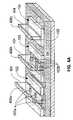
- FIG. 4Aillustrates gates 402 a and 402 b and 408 that are formed around the nanowires 110 a , 110 b , and over SOI slab 105 , as described in further detail below, and capped with polysilicon layer 404 .
- Hardmask lines 406 a , 406 b and 406 care defined by patterning, for example a silicon nitride (Si 3 N 4 ) layer that is deposited over the polysilicon layer 404 .
- the polysilicon layer 404 and the hardmask lines 406 a 406 b , and 406 cmay be formed by depositing polysilicon material over the BOX layer 104 and the SOI portions 102 , 103 and 105 , depositing the hardmask material over the polysilicon material, and etching by RIE to form the polysilicon lines 404 a , 404 b , and 404 c illustrated in FIG. 4A .
- the etching of the gates 402 a , 402 b , and 408may be performed by directional etching that results in straight sidewalls of the gates 402 a , 402 b , and 408 .
- polysilicon 404 aremains under the nanowires 110 a in regions not masked by the hardmask 406 a . Isotropic etching may be performed to remove polysilicon 404 a from under the nanowires 110 a .
- the gate stack 402 a , 402 b , and 408is formed by depositing a conformal gate dielectric film 502 a such SiO 2 , SiON, or HfO 2 (or other hi-K material) around the nanowires.
- a second conformal gate dielectric film 504 amay also be applied.
- a metal gate film 506 asuch as, for example, TaN or TiN is deposited over the gate dielectric.
- Poly-silicon 404is deposited over the metal gate film of the gates.
- FIG. 4Billustrates the nanowires 110 a and 110 b that are formed using a similar process as described above in FIG. 4A following the oxidation process of FIG. 3B .
- FIG. 5Aillustrates a cross sectional view of a gate 402 a along the line A-A (of FIG. 4B ).
- the gate 402 ais formed by depositing a first gate dielectric layer 502 a , such as silicon dioxide (SiO 2 ) around the nanowire 110 a .
- a second gate dielectric layer 504 asuch as, for example, hafnium oxide (HfO 2 ) is formed around the silicon oxide layer 502 a .
- a metal layer 506 asuch as, for example, tantalum nitride (TaN) is formed around the dielectric layer 504 a .
- the metal layer 506 ais surrounded by polysilicon layer 404 a (of FIG. 4B ). Doping the polysilicon layer 404 a with impurities such as boron (p-type), or phosphorus (n-type) makes the polysilicon layer 404 a conductive.
- FIG. 5Billustrates a cross sectional view of a gate 402 b along the line B-B of FIG. 4B formed by a similar process as described above, and including first gate dielectric layer 502 b around the nanowire 110 b , second gate dielectric layer 504 b , and a metal layer 506 b surrounded by the polysilicon layer 404 b .
- the gate stack 408includes the dielectric layer disposed on the SOI portion 105 , the second gate dielectric layer 504 , and the metal layer 506 that is capped by poly-silicon 404 . Since the channel of device 105 is planar as it forms in a planar SOI slab, the films comprising gate stack 408 also have a planar geometry.
- FIGS. 6A and 6Billustrate the spacer portions 604 a , 604 b , and 604 c formed along opposing sides of the polysilicon lines 404 a , 404 b , and 404 c .
- the spacers 604 a , 604 b , and 604 care formed by depositing a blanket dielectric film such as silicon nitride and etching the dielectric film from all horizontal surfaces by RIE.
- the spacers 604 a and 604 bare formed around portions of the nanowires 110 a and 110 b that extend from the polysilicon layers 404 a and 104 b and surround portions of the nanowires 110 a and 110 b .
- FIG. 6Aincludes spacer portions 602 a and 602 b that are formed under the nanowires 110 a , and in the undercut regions 202 (of FIG. 2 ).
- FIG. 7illustrates the resultant structures (of FIGS. 6A and 6B ) following a selective epi-silicon growth that thickens the exposed nanowire portions not covered by the gate 404 a and 404 b and spacers 604 .
- the epitaxial growth 702thickens the SOI pads 106 a , 108 a , 106 b , 108 b and portions of SOI 105 not covered by the gate 404 c and spacers 604 c .
- the epitaxial growthmay merge the adjacent nanowires 110 together with epi-silicon.
- the thickened/merged nanowires and SOI regionsare formed by epitaxially growing, for example, in-situ doped silicon (Si) or a silicon germanium (SiGe) that may be either n-type or p-type doped.
- the in-situ doped epi processforms the source region and the drain region of the nanowire FET.
- a chemical vapor deposition (CVD) reactormay be used to perform the epitaxial growth.
- Precursors for silicon epitaxyinclude SiCl 4 , SiH 4 combined with HCL. The use of chlorine allows selective deposition of silicon only on exposed silicon surfaces.
- a precursor for SiGemay be GeH 4 , which may obtain deposition selectivity without HCL.
- Precursors for dopantsmay include PH 3 or AsH 3 for n-type doping and B 2 H 6 for p-type doping.
- Deposition temperaturesmay range from 550 C to 1000 C for pure silicon deposition, and as low as 300 C for pure Ge deposition.
- FIG. 8illustrates a resultant structure following silicidation where a silicide 802 is formed on the exposed epitaxy 702 .
- silicide forming metalsinclude Ni, Pt, Co, and alloys such as NiPt. When Ni is used the NiSi phase is formed due to its low resistivity. For example, formation temperatures include 400-600° C.
Landscapes
- Engineering & Computer Science (AREA)
- Chemical & Material Sciences (AREA)
- Nanotechnology (AREA)
- Crystallography & Structural Chemistry (AREA)
- Physics & Mathematics (AREA)
- Mathematical Physics (AREA)
- Theoretical Computer Science (AREA)
- Condensed Matter Physics & Semiconductors (AREA)
- General Physics & Mathematics (AREA)
- Manufacturing & Machinery (AREA)
- Thin Film Transistor (AREA)
Abstract
Description
Claims (20)
Priority Applications (2)
| Application Number | Priority Date | Filing Date | Title |
|---|---|---|---|
| US12/631,342US8455334B2 (en) | 2009-12-04 | 2009-12-04 | Planar and nanowire field effect transistors |
| US13/600,598US9184301B2 (en) | 2009-12-04 | 2012-08-31 | Planar and nanowire field effect transistors |
Applications Claiming Priority (1)
| Application Number | Priority Date | Filing Date | Title |
|---|---|---|---|
| US12/631,342US8455334B2 (en) | 2009-12-04 | 2009-12-04 | Planar and nanowire field effect transistors |
Related Child Applications (1)
| Application Number | Title | Priority Date | Filing Date |
|---|---|---|---|
| US13/600,598ContinuationUS9184301B2 (en) | 2009-12-04 | 2012-08-31 | Planar and nanowire field effect transistors |
Publications (2)
| Publication Number | Publication Date |
|---|---|
| US20110133167A1 US20110133167A1 (en) | 2011-06-09 |
| US8455334B2true US8455334B2 (en) | 2013-06-04 |
Family
ID=44081139
Family Applications (2)
| Application Number | Title | Priority Date | Filing Date |
|---|---|---|---|
| US12/631,342Expired - Fee RelatedUS8455334B2 (en) | 2009-12-04 | 2009-12-04 | Planar and nanowire field effect transistors |
| US13/600,598Active2030-07-13US9184301B2 (en) | 2009-12-04 | 2012-08-31 | Planar and nanowire field effect transistors |
Family Applications After (1)
| Application Number | Title | Priority Date | Filing Date |
|---|---|---|---|
| US13/600,598Active2030-07-13US9184301B2 (en) | 2009-12-04 | 2012-08-31 | Planar and nanowire field effect transistors |
Country Status (1)
| Country | Link |
|---|---|
| US (2) | US8455334B2 (en) |
Cited By (5)
| Publication number | Priority date | Publication date | Assignee | Title |
|---|---|---|---|---|
| US20100151659A1 (en)* | 2008-12-16 | 2010-06-17 | Samsung Electronics Co, Ltd. | Method of forming core-shell type structure and method of manufacturing transistor using the same |
| US20150325648A1 (en)* | 2011-12-23 | 2015-11-12 | Stephen M. Cea | Nanowire structures having non-discrete source and drain regions |
| US9601569B1 (en) | 2015-12-07 | 2017-03-21 | Samsung Electronics Co., Ltd. | Semiconductor device having a gate all around structure |
| US9704861B2 (en) | 2013-08-01 | 2017-07-11 | Taiwan Semiconductor Manufacturing Company, Ltd. | Semiconductor device and fabricating the same |
| US9899515B1 (en) | 2016-10-31 | 2018-02-20 | International Business Machines Corporation | Fabrication of a pair of vertical fin field effect transistors having a merged top source/drain |
Families Citing this family (43)
| Publication number | Priority date | Publication date | Assignee | Title |
|---|---|---|---|---|
| US8455334B2 (en) | 2009-12-04 | 2013-06-04 | International Business Machines Corporation | Planar and nanowire field effect transistors |
| US8722492B2 (en) | 2010-01-08 | 2014-05-13 | International Business Machines Corporation | Nanowire pin tunnel field effect devices |
| US8361907B2 (en)* | 2010-05-10 | 2013-01-29 | International Business Machines Corporation | Directionally etched nanowire field effect transistors |
| US8394710B2 (en)* | 2010-06-21 | 2013-03-12 | International Business Machines Corporation | Semiconductor devices fabricated by doped material layer as dopant source |
| US8835231B2 (en) | 2010-08-16 | 2014-09-16 | International Business Machines Corporation | Methods of forming contacts for nanowire field effect transistors |
| US8716072B2 (en)* | 2011-07-25 | 2014-05-06 | International Business Machines Corporation | Hybrid CMOS technology with nanowire devices and double gated planar devices |
| US20130109167A1 (en) | 2011-11-01 | 2013-05-02 | International Business Machines Corporation | Nanowire efuses |
| US8709888B2 (en)* | 2011-12-16 | 2014-04-29 | International Business Machines Corporation | Hybrid CMOS nanowire mesh device and PDSOI device |
| US8722472B2 (en) | 2011-12-16 | 2014-05-13 | International Business Machines Corporation | Hybrid CMOS nanowire mesh device and FINFET device |
| US8563376B2 (en)* | 2011-12-16 | 2013-10-22 | International Business Machines Corporation | Hybrid CMOS nanowire mesh device and bulk CMOS device |
| WO2013095341A1 (en) | 2011-12-19 | 2013-06-27 | Intel Corporation | Cmos implementation of germanium and iii-v nanowires and nanoribbons in gate-all-around architecture |
| US8896066B2 (en) | 2011-12-20 | 2014-11-25 | Intel Corporation | Tin doped III-V material contacts |
| KR101891458B1 (en)* | 2011-12-20 | 2018-08-24 | 인텔 코포레이션 | Semiconductor device having iii-v semiconductor material layer |
| US8901659B2 (en) | 2012-02-09 | 2014-12-02 | International Business Machines Corporation | Tapered nanowire structure with reduced off current |
| US8698128B2 (en) | 2012-02-27 | 2014-04-15 | International Business Machines Corporation | Gate-all around semiconductor nanowire FET's on bulk semicoductor wafers |
| US8575009B2 (en) | 2012-03-08 | 2013-11-05 | International Business Machines Corporation | Two-step hydrogen annealing process for creating uniform non-planar semiconductor devices at aggressive pitch |
| US9006810B2 (en) | 2012-06-07 | 2015-04-14 | International Business Machines Corporation | DRAM with a nanowire access transistor |
| US8536029B1 (en)* | 2012-06-21 | 2013-09-17 | International Business Machines Corporation | Nanowire FET and finFET |
| KR102002380B1 (en) | 2012-10-10 | 2019-07-23 | 삼성전자 주식회사 | Semiconductor device and fabricated method thereof |
| FR3005309B1 (en) | 2013-05-02 | 2016-03-11 | Commissariat Energie Atomique | NANOWELL AND PLANNER TRANSISTORS COINTEGRATED ON SUBSTRATE SOI UTBOX |
| US9171843B2 (en) | 2013-08-02 | 2015-10-27 | Taiwan Semiconductor Manufacturing Company, Ltd. | Semiconductor device and fabricating the same |
| US11404325B2 (en) | 2013-08-20 | 2022-08-02 | Taiwan Semiconductor Manufacturing Co., Ltd. | Silicon and silicon germanium nanowire formation |
| US9184269B2 (en)* | 2013-08-20 | 2015-11-10 | Taiwan Semiconductor Manufacturing Company Limited | Silicon and silicon germanium nanowire formation |
| US8872161B1 (en)* | 2013-08-26 | 2014-10-28 | Taiwan Semiconductor Manufacturing Company, Ltd. | Integrate circuit with nanowires |
| US20150145042A1 (en)* | 2013-11-25 | 2015-05-28 | International Business Machines Corporation | Transistors having multiple lateral channel dimensions |
| US9595525B2 (en)* | 2014-02-10 | 2017-03-14 | International Business Machines Corporation | Semiconductor device including nanowire transistors with hybrid channels |
| US9166025B1 (en)* | 2014-06-13 | 2015-10-20 | Globalfoundries Inc. | Methods of forming a nanowire device with a gate-all-around-channel configuration and the resulting nanowire device |
| US9443949B1 (en) | 2015-03-27 | 2016-09-13 | International Business Machines Corporation | Techniques for multiple gate workfunctions for a nanowire CMOS technology |
| KR101615723B1 (en)* | 2015-07-29 | 2016-04-28 | 울산과학기술원 | Nanowire for anode material of lithium ion cell and manufacturing method thereof |
| US10032678B2 (en) | 2015-10-15 | 2018-07-24 | Qualcomm Incorporated | Nanowire channel structures of continuously stacked nanowires for complementary metal oxide semiconductor (CMOS) devices |
| US9472555B1 (en)* | 2015-12-19 | 2016-10-18 | International Business Machines Corporation | Nanosheet CMOS with hybrid orientation |
| KR102416133B1 (en)* | 2016-01-11 | 2022-07-01 | 삼성전자주식회사 | Semiconductor device and fabricated method thereof |
| CN106960870B (en) | 2016-01-11 | 2021-09-10 | 三星电子株式会社 | Semiconductor device and method for manufacturing the same |
| CN107204311A (en)* | 2016-03-16 | 2017-09-26 | 上海新昇半导体科技有限公司 | Nanowire semiconductor device and its manufacture method |
| US9643179B1 (en)* | 2016-06-24 | 2017-05-09 | International Business Machines Corporation | Techniques for fabricating horizontally aligned nanochannels for microfluidics and biosensors |
| CN106057664B (en)* | 2016-07-27 | 2019-04-02 | 北京大学 | A kind of preparation method of nanoscale polysilicon lines |
| CN107845679A (en)* | 2016-09-20 | 2018-03-27 | 上海新昇半导体科技有限公司 | A kind of ring grid field effect transistor based on negative capacitance and preparation method thereof |
| KR102530338B1 (en) | 2016-12-15 | 2023-05-08 | 삼성전자주식회사 | Semiconductor device and method for fabricating the same |
| US10475929B2 (en)* | 2017-11-30 | 2019-11-12 | Taiwan Semiconductor Manufacturing Co., Ltd. | Semiconductor device and manufacturing method thereof |
| TWI707972B (en)* | 2018-05-03 | 2020-10-21 | 國立交通大學 | Method for forming nano sensing chip by selective deposition of sensing materials through device-localized joule heating and nano sensing chip thereof |
| US11362001B2 (en)* | 2018-08-14 | 2022-06-14 | Taiwan Semiconductor Manufacturing Co., Ltd. | Method for manufacturing nanostructures with various widths |
| KR20220107847A (en)* | 2021-01-26 | 2022-08-02 | 삼성전자주식회사 | Integrated circuit device and method of manufacturing the same |
| US12100766B2 (en) | 2021-11-03 | 2024-09-24 | International Business Machines Corporation | Integrated short channel omega gate FinFET and long channel FinFET |
Citations (83)
| Publication number | Priority date | Publication date | Assignee | Title |
|---|---|---|---|---|
| EP0217811A1 (en) | 1985-03-18 | 1987-04-15 | Caterpillar Inc | Engine having a multipiece cylinder block. |
| US4995001A (en) | 1988-10-31 | 1991-02-19 | International Business Machines Corporation | Memory cell and read circuit |
| US5308445A (en) | 1991-10-23 | 1994-05-03 | Rohm Co., Ltd. | Method of manufacturing a semiconductor device having a semiconductor growth layer completely insulated from a substrate |
| US5438018A (en) | 1992-12-07 | 1995-08-01 | Fujitsu Limited | Method of making semiconductor device by selective epitaxial growth |
| US5552622A (en) | 1992-07-14 | 1996-09-03 | Mitsuteru Kimura | Tunnel transistor |
| US5668046A (en) | 1991-03-27 | 1997-09-16 | Nec Corporation | Method of producing a semiconductor on insulating substrate, and a method of forming transistor thereon |
| US6365465B1 (en) | 1999-03-19 | 2002-04-02 | International Business Machines Corporation | Self-aligned double-gate MOSFET by selective epitaxy and silicon wafer bonding techniques |
| WO2002084757A1 (en) | 2001-04-12 | 2002-10-24 | Infineon Technologies Ag | Heterostructure component |
| US6642115B1 (en) | 2000-05-15 | 2003-11-04 | International Business Machines Corporation | Double-gate FET with planarized surfaces and self-aligned silicides |
| US6653209B1 (en) | 1999-09-30 | 2003-11-25 | Canon Kabushiki Kaisha | Method of producing silicon thin film, method of constructing SOI substrate and semiconductor device |
| US20040149978A1 (en) | 2003-01-31 | 2004-08-05 | Greg Snider | Molecular-junction-nanowire-crossbar-based inverter, latch, and flip-flop circuits, and more complex circuits composed, in part, from molecular-junction-nanowire-crossbar-based inverter, latch, and flip-flop circuits |
| US20040166642A1 (en) | 2003-02-20 | 2004-08-26 | Hao-Yu Chen | Semiconductor nano-rod devices |
| US6806141B2 (en) | 2002-05-22 | 2004-10-19 | Hewlett-Packard Development Company, L.P. | Field effect transistor with gate layer and method of making same |
| US6835618B1 (en) | 2003-08-05 | 2004-12-28 | Advanced Micro Devices, Inc. | Epitaxially grown fin for FinFET |
| US6882051B2 (en) | 2001-03-30 | 2005-04-19 | The Regents Of The University Of California | Nanowires, nanostructures and devices fabricated therefrom |
| US6891227B2 (en) | 2002-03-20 | 2005-05-10 | International Business Machines Corporation | Self-aligned nanotube field effect transistor and method of fabricating same |
| US6903013B2 (en) | 2003-05-16 | 2005-06-07 | Chartered Semiconductor Manufacturing Ltd. | Method to fill a trench and tunnel by using ALD seed layer and electroless plating |
| US20050266645A1 (en) | 2004-05-25 | 2005-12-01 | Jin-Jun Park | Phosphorous doping methods of manufacturing field effect transistors having multiple stacked channels |
| US20050275010A1 (en) | 2004-06-10 | 2005-12-15 | Hung-Wei Chen | Semiconductor nano-wire devices and methods of fabrication |
| US20060033145A1 (en) | 2004-08-13 | 2006-02-16 | Ronald Kakoschke | Integrated memory device and process |
| US20060138552A1 (en) | 2004-09-30 | 2006-06-29 | Brask Justin K | Nonplanar transistors with metal gate electrodes |
| US7101762B2 (en) | 2000-07-07 | 2006-09-05 | International Business Machines Corporation | Self-aligned double gate mosfet with separate gates |
| US7151209B2 (en) | 2002-04-02 | 2006-12-19 | Nanosys, Inc. | Methods of making, positioning and orienting nanostructures, nanostructure arrays and nanostructure devices |
| US20070001219A1 (en) | 2005-06-30 | 2007-01-04 | Marko Radosavljevic | Block contact architectures for nanoscale channel transistors |
| US7180107B2 (en) | 2004-05-25 | 2007-02-20 | International Business Machines Corporation | Method of fabricating a tunneling nanotube field effect transistor |
| US7211853B2 (en) | 2001-07-26 | 2007-05-01 | Technische Universiteit Delft | Electronic device using carbon nanotubes |
| US7253060B2 (en) | 2004-06-08 | 2007-08-07 | Samsung Electronics Co., Ltd. | Gate-all-around type of semiconductor device and method of fabricating the same |
| US7297615B2 (en) | 2005-05-13 | 2007-11-20 | Samsung Electronics, Co., Ltd. | Si nanowire substrate, method of manufacturing the same, and method of manufacturing thin film transistor using the same |
| US20070267619A1 (en) | 2006-05-22 | 2007-11-22 | Thomas Nirschl | Memory using tunneling field effect transistors |
| US20070267703A1 (en) | 2006-05-17 | 2007-11-22 | Chartered Semiconductor Manufacturing Ltd. | Strained channel transistor and method of fabrication thereof |
| US20070284613A1 (en) | 2006-06-09 | 2007-12-13 | Chi On Chui | Strain-inducing semiconductor regions |
| US7311776B2 (en) | 2003-12-30 | 2007-12-25 | The Regents Of The University Of California | Localized synthesis and self-assembly of nanostructures |
| US20080014689A1 (en) | 2006-07-07 | 2008-01-17 | Texas Instruments Incorporated | Method for making planar nanowire surround gate mosfet |
| US20080061284A1 (en) | 2006-09-11 | 2008-03-13 | International Business Machines Corporation | Nanowire MOSFET with doped epitaxial contacts for source and drain |
| US20080067495A1 (en) | 2006-09-15 | 2008-03-20 | Interuniversitair Microelektronica Centrum (Imec) | Tunnel effect transistors based on silicon nanowires |
| US20080067607A1 (en) | 2006-09-15 | 2008-03-20 | Interuniversitair Microelektronica Centrum (Imec) | Tunnel effect transistors based on elongate monocrystalline nanostructures having a heterostructure |
| US20080079041A1 (en) | 2006-10-02 | 2008-04-03 | Samsung Electronics Co, Ltd. | Gate-all-around type semiconductor device and method of manufacturing the same |
| US20080085587A1 (en) | 2006-10-04 | 2008-04-10 | Micron Technology, Inc. | Epitaxial silicon growth |
| US20080121932A1 (en) | 2006-09-18 | 2008-05-29 | Pushkar Ranade | Active regions with compatible dielectric layers |
| US20080128760A1 (en) | 2006-12-04 | 2008-06-05 | Electronics And Telecommunications Research Institute | Schottky barrier nanowire field effect transistor and method for fabricating the same |
| WO2008069765A1 (en) | 2006-12-08 | 2008-06-12 | Agency For Science, Technology And Research | A stacked silicon-germanium nanowire structure and a method of forming the same |
| US20080142853A1 (en) | 2005-08-08 | 2008-06-19 | Freescale Semiconductor, Inc. | Multi-channel transistor structure and method of making thereof |
| US20080149914A1 (en) | 2006-12-22 | 2008-06-26 | Qunano Ab | Nanoelectronic structure and method of producing such |
| US20080150025A1 (en) | 2005-12-13 | 2008-06-26 | Versatilis Llc | Methods of Making Semiconductor-Based Electronic Devices on a Wire and by Forming Freestanding Semiconductor Structures, and Devices That Can Be Made Thereby |
| US20080149997A1 (en) | 2006-12-20 | 2008-06-26 | Samsung Electronics Co., Ltd. | Nonvolatile memory device and method of operating the same |
| US20080179752A1 (en) | 2007-01-26 | 2008-07-31 | Takashi Yamauchi | Method of making semiconductor device and semiconductor device |
| US20080191196A1 (en) | 2005-06-06 | 2008-08-14 | Wei Lu | Nanowire heterostructures |
| US20080224224A1 (en) | 2007-03-12 | 2008-09-18 | Interuniversitair Microelektronica Centrum Vzw (Imec) | Tunnel field-effect transistor with gated tunnel barrier |
| US20080227259A1 (en) | 2005-01-07 | 2008-09-18 | International Business Machines Corporation | SELF-ALIGNED PROCESS FOR NANOTUBE/NANOWIRE FETs |
| US20080246021A1 (en) | 2006-10-04 | 2008-10-09 | Samsung Electronic Co., Ltd., | Single electron transistor and method of manufacturing the same |
| US20080247226A1 (en) | 2007-04-05 | 2008-10-09 | Micron Technology, Inc. | Memory devices having electrodes comprising nanowires, systems including same and methods of forming same |
| US7443025B2 (en) | 2004-06-07 | 2008-10-28 | Broadcom Corporation | Thermally improved placement of power-dissipating components onto a circuit board |
| US7446025B2 (en) | 2005-05-23 | 2008-11-04 | International Business Machines Corporation | Method of forming vertical FET with nanowire channels and a silicided bottom contact |
| US7449373B2 (en) | 2006-03-31 | 2008-11-11 | Intel Corporation | Method of ion implanting for tri-gate devices |
| US7452759B2 (en) | 2005-11-29 | 2008-11-18 | Micron Technology, Inc. | Carbon nanotube field effect transistor and methods for making same |
| US7456476B2 (en) | 2003-06-27 | 2008-11-25 | Intel Corporation | Nonplanar semiconductor device with partially or fully wrapped around gate electrode and methods of fabrication |
| US7456068B2 (en) | 2006-06-08 | 2008-11-25 | Intel Corporation | Forming ultra-shallow junctions |
| US20080290418A1 (en) | 2007-05-25 | 2008-11-27 | Kalburge Amol M | Method for Integrating Nanotube Devices with CMOS for RF/Analog SoC Applications |
| US7473943B2 (en) | 2004-10-15 | 2009-01-06 | Nanosys, Inc. | Gate configuration for nanowire electronic devices |
| US20090026553A1 (en) | 2007-07-25 | 2009-01-29 | Krishna Kumar Bhuwalka | Tunnel Field-Effect Transistor with Narrow Band-Gap Channel and Strong Gate Coupling |
| US7498211B2 (en) | 2005-12-28 | 2009-03-03 | Intel Corporation | Independently controlled, double gate nanowire memory cell with self-aligned contacts |
| US20090057650A1 (en) | 2000-08-22 | 2009-03-05 | President And Fellows Of Harvard College | Nanoscale wires and related devices |
| US20090057762A1 (en) | 2007-09-05 | 2009-03-05 | International Business Machines Corporation | Nanowire Field-Effect Transistors |
| US20090061568A1 (en) | 2007-09-05 | 2009-03-05 | International Business Machines Corporation | Techniques for Fabricating Nanowire Field-Effect Transistors |
| US20090090934A1 (en) | 2007-10-05 | 2009-04-09 | Tsutomu Tezuka | Field Effect Transistor and Method for Manufacturing the Same |
| KR20090044799A (en) | 2007-11-01 | 2009-05-07 | 삼성전자주식회사 | Method for manufacturing active fin and transistor comprising same |
| US20090134467A1 (en) | 2007-11-26 | 2009-05-28 | Renesas Technology Corp. | Semiconductor device and a method of manufacturing the same |
| US7550333B2 (en) | 2004-10-25 | 2009-06-23 | Intel Corporation | Nonplanar device with thinned lower body portion and method of fabrication |
| US20090181477A1 (en) | 2005-07-01 | 2009-07-16 | Synopsys, Inc. | Integrated Circuit On Corrugated Substrate |
| US20090217216A1 (en) | 2007-02-28 | 2009-08-27 | Motorola, Inc. | Carbon nanotube circuits design methodology |
| US20090294864A1 (en) | 2005-06-13 | 2009-12-03 | Samsung Electronics Co., Ltd. | Mos field effect transistor having plurality of channels |
| US7642578B2 (en) | 2005-03-24 | 2010-01-05 | Samsung Electronics Co., Ltd. | Semiconductor device having a round-shaped nano-wire transistor channel and method of manufacturing same |
| US20100193770A1 (en) | 2009-02-04 | 2010-08-05 | International Business Machines Corporation | Maskless Process for Suspending and Thinning Nanowires |
| US20100207102A1 (en) | 2009-02-18 | 2010-08-19 | Samsung Electronics Co., Ltd. | Static random access memories having carbon nanotube thin films |
| US7791144B2 (en) | 2006-04-28 | 2010-09-07 | International Business Machines Corporation | High performance stress-enhance MOSFET and method of manufacture |
| US7799657B2 (en) | 2005-06-07 | 2010-09-21 | Freescale Semiconductor, Inc. | Method of fabricating a substrate for a planar, double-gated, transistor process |
| US7834345B2 (en) | 2008-09-05 | 2010-11-16 | Taiwan Semiconductor Manufacturing Company, Ltd. | Tunnel field-effect transistors with superlattice channels |
| US7893506B2 (en) | 2005-02-23 | 2011-02-22 | Intel Corporation | Field effect transistor with narrow bandgap source and drain regions and method of fabrication |
| US20110133169A1 (en) | 2009-12-04 | 2011-06-09 | International Business Machines Corporation | Gate-All-Around Nanowire Tunnel Field Effect Transistors |
| US20110147840A1 (en) | 2009-12-23 | 2011-06-23 | Cea Stephen M | Wrap-around contacts for finfet and tri-gate devices |
| US8154127B1 (en)* | 2007-07-30 | 2012-04-10 | Hewlett-Packard Development Company, L.P. | Optical device and method of making the same |
| US8338280B2 (en)* | 2010-07-08 | 2012-12-25 | Globalfoundries Singapore Pte. Ltd. | Method for fabricating nano devices |
| US20130001517A1 (en)* | 2010-05-12 | 2013-01-03 | International Business Machines Corporation | Generation of multiple diameter nanowire field effect transistors |
Family Cites Families (15)
| Publication number | Priority date | Publication date | Assignee | Title |
|---|---|---|---|---|
| AU1525400A (en) | 1998-11-18 | 2000-06-05 | Microdexterity Systems, Inc. | Medical manipulator for use with an imaging device |
| US6867433B2 (en)* | 2003-04-30 | 2005-03-15 | Taiwan Semiconductor Manufacturing Company, Ltd. | Semiconductor-on-insulator chip incorporating strained-channel partially-depleted, fully-depleted, and multiple-gate transistors |
| US6911383B2 (en)* | 2003-06-26 | 2005-06-28 | International Business Machines Corporation | Hybrid planar and finFET CMOS devices |
| US7335934B2 (en)* | 2003-07-22 | 2008-02-26 | Innovative Silicon S.A. | Integrated circuit device, and method of fabricating same |
| US7060576B2 (en) | 2003-10-24 | 2006-06-13 | Intel Corporation | Epitaxially deposited source/drain |
| US7402872B2 (en) | 2004-11-18 | 2008-07-22 | Intel Corporation | Method for forming an integrated circuit |
| KR100745769B1 (en) | 2006-09-11 | 2007-08-02 | 삼성전자주식회사 | Nanowire electromechanical switching device and manufacturing method thereof, electromechanical memory device using the nanowire electromechanical device |
| JP2008172082A (en)* | 2007-01-12 | 2008-07-24 | Toshiba Corp | Semiconductor device and manufacturing method of semiconductor device |
| KR101014926B1 (en)* | 2008-05-20 | 2011-02-15 | 주식회사 하이닉스반도체 | Program Verification Method of Nonvolatile Memory Device |
| US8362604B2 (en) | 2008-12-04 | 2013-01-29 | Ecole Polytechnique Federale De Lausanne (Epfl) | Ferroelectric tunnel FET switch and memory |
| US8368125B2 (en) | 2009-07-20 | 2013-02-05 | International Business Machines Corporation | Multiple orientation nanowires with gate stack stressors |
| US8129247B2 (en) | 2009-12-04 | 2012-03-06 | International Business Machines Corporation | Omega shaped nanowire field effect transistors |
| US8455334B2 (en) | 2009-12-04 | 2013-06-04 | International Business Machines Corporation | Planar and nanowire field effect transistors |
| US8097515B2 (en) | 2009-12-04 | 2012-01-17 | International Business Machines Corporation | Self-aligned contacts for nanowire field effect transistors |
| US8716072B2 (en) | 2011-07-25 | 2014-05-06 | International Business Machines Corporation | Hybrid CMOS technology with nanowire devices and double gated planar devices |
- 2009
- 2009-12-04USUS12/631,342patent/US8455334B2/ennot_activeExpired - Fee Related
- 2012
- 2012-08-31USUS13/600,598patent/US9184301B2/enactiveActive
Patent Citations (93)
| Publication number | Priority date | Publication date | Assignee | Title |
|---|---|---|---|---|
| EP0217811A1 (en) | 1985-03-18 | 1987-04-15 | Caterpillar Inc | Engine having a multipiece cylinder block. |
| US4995001A (en) | 1988-10-31 | 1991-02-19 | International Business Machines Corporation | Memory cell and read circuit |
| US5668046A (en) | 1991-03-27 | 1997-09-16 | Nec Corporation | Method of producing a semiconductor on insulating substrate, and a method of forming transistor thereon |
| US5308445A (en) | 1991-10-23 | 1994-05-03 | Rohm Co., Ltd. | Method of manufacturing a semiconductor device having a semiconductor growth layer completely insulated from a substrate |
| US5552622A (en) | 1992-07-14 | 1996-09-03 | Mitsuteru Kimura | Tunnel transistor |
| US5438018A (en) | 1992-12-07 | 1995-08-01 | Fujitsu Limited | Method of making semiconductor device by selective epitaxial growth |
| US5574308A (en) | 1992-12-07 | 1996-11-12 | Fujitsu Limited | Semiconductor device and its manufacturing method |
| US6365465B1 (en) | 1999-03-19 | 2002-04-02 | International Business Machines Corporation | Self-aligned double-gate MOSFET by selective epitaxy and silicon wafer bonding techniques |
| US6653209B1 (en) | 1999-09-30 | 2003-11-25 | Canon Kabushiki Kaisha | Method of producing silicon thin film, method of constructing SOI substrate and semiconductor device |
| US6642115B1 (en) | 2000-05-15 | 2003-11-04 | International Business Machines Corporation | Double-gate FET with planarized surfaces and self-aligned silicides |
| US7101762B2 (en) | 2000-07-07 | 2006-09-05 | International Business Machines Corporation | Self-aligned double gate mosfet with separate gates |
| US20090057650A1 (en) | 2000-08-22 | 2009-03-05 | President And Fellows Of Harvard College | Nanoscale wires and related devices |
| US7569941B2 (en) | 2001-03-30 | 2009-08-04 | The Regents Of The University Of California | Methods of fabricating nanostructures and nanowires and devices fabricated therefrom |
| US6996147B2 (en) | 2001-03-30 | 2006-02-07 | The Regents Of The University Of California | Methods of fabricating nanostructures and nanowires and devices fabricated therefrom |
| US6882051B2 (en) | 2001-03-30 | 2005-04-19 | The Regents Of The University Of California | Nanowires, nanostructures and devices fabricated therefrom |
| WO2002084757A1 (en) | 2001-04-12 | 2002-10-24 | Infineon Technologies Ag | Heterostructure component |
| US7211853B2 (en) | 2001-07-26 | 2007-05-01 | Technische Universiteit Delft | Electronic device using carbon nanotubes |
| US6891227B2 (en) | 2002-03-20 | 2005-05-10 | International Business Machines Corporation | Self-aligned nanotube field effect transistor and method of fabricating same |
| US7151209B2 (en) | 2002-04-02 | 2006-12-19 | Nanosys, Inc. | Methods of making, positioning and orienting nanostructures, nanostructure arrays and nanostructure devices |
| US6806141B2 (en) | 2002-05-22 | 2004-10-19 | Hewlett-Packard Development Company, L.P. | Field effect transistor with gate layer and method of making same |
| US20040149978A1 (en) | 2003-01-31 | 2004-08-05 | Greg Snider | Molecular-junction-nanowire-crossbar-based inverter, latch, and flip-flop circuits, and more complex circuits composed, in part, from molecular-junction-nanowire-crossbar-based inverter, latch, and flip-flop circuits |
| US20050121706A1 (en) | 2003-02-20 | 2005-06-09 | Hao-Yu Chen | Semiconductor nano-rod devices |
| US20040166642A1 (en) | 2003-02-20 | 2004-08-26 | Hao-Yu Chen | Semiconductor nano-rod devices |
| US6855606B2 (en) | 2003-02-20 | 2005-02-15 | Taiwan Semiconductor Manufacturing Company, Ltd. | Semiconductor nano-rod devices |
| US6903013B2 (en) | 2003-05-16 | 2005-06-07 | Chartered Semiconductor Manufacturing Ltd. | Method to fill a trench and tunnel by using ALD seed layer and electroless plating |
| US7456476B2 (en) | 2003-06-27 | 2008-11-25 | Intel Corporation | Nonplanar semiconductor device with partially or fully wrapped around gate electrode and methods of fabrication |
| US6835618B1 (en) | 2003-08-05 | 2004-12-28 | Advanced Micro Devices, Inc. | Epitaxially grown fin for FinFET |
| US7311776B2 (en) | 2003-12-30 | 2007-12-25 | The Regents Of The University Of California | Localized synthesis and self-assembly of nanostructures |
| US20050266645A1 (en) | 2004-05-25 | 2005-12-01 | Jin-Jun Park | Phosphorous doping methods of manufacturing field effect transistors having multiple stacked channels |
| US7180107B2 (en) | 2004-05-25 | 2007-02-20 | International Business Machines Corporation | Method of fabricating a tunneling nanotube field effect transistor |
| US7443025B2 (en) | 2004-06-07 | 2008-10-28 | Broadcom Corporation | Thermally improved placement of power-dissipating components onto a circuit board |
| US7253060B2 (en) | 2004-06-08 | 2007-08-07 | Samsung Electronics Co., Ltd. | Gate-all-around type of semiconductor device and method of fabricating the same |
| US20050275010A1 (en) | 2004-06-10 | 2005-12-15 | Hung-Wei Chen | Semiconductor nano-wire devices and methods of fabrication |
| US7452778B2 (en) | 2004-06-10 | 2008-11-18 | Taiwan Semiconductor Manufacturing Company, Ltd. | Semiconductor nano-wire devices and methods of fabrication |
| US20060033145A1 (en) | 2004-08-13 | 2006-02-16 | Ronald Kakoschke | Integrated memory device and process |
| US20060138552A1 (en) | 2004-09-30 | 2006-06-29 | Brask Justin K | Nonplanar transistors with metal gate electrodes |
| US20090149012A1 (en) | 2004-09-30 | 2009-06-11 | Brask Justin K | Method of forming a nonplanar transistor with sidewall spacers |
| US7473943B2 (en) | 2004-10-15 | 2009-01-06 | Nanosys, Inc. | Gate configuration for nanowire electronic devices |
| US7871870B2 (en) | 2004-10-15 | 2011-01-18 | Nanosys, Inc. | Method of fabricating gate configurations for an improved contacts in nanowire based electronic devices |
| US7550333B2 (en) | 2004-10-25 | 2009-06-23 | Intel Corporation | Nonplanar device with thinned lower body portion and method of fabrication |
| US20080227259A1 (en) | 2005-01-07 | 2008-09-18 | International Business Machines Corporation | SELF-ALIGNED PROCESS FOR NANOTUBE/NANOWIRE FETs |
| US7893506B2 (en) | 2005-02-23 | 2011-02-22 | Intel Corporation | Field effect transistor with narrow bandgap source and drain regions and method of fabrication |
| US7642578B2 (en) | 2005-03-24 | 2010-01-05 | Samsung Electronics Co., Ltd. | Semiconductor device having a round-shaped nano-wire transistor channel and method of manufacturing same |
| US7297615B2 (en) | 2005-05-13 | 2007-11-20 | Samsung Electronics, Co., Ltd. | Si nanowire substrate, method of manufacturing the same, and method of manufacturing thin film transistor using the same |
| US7446025B2 (en) | 2005-05-23 | 2008-11-04 | International Business Machines Corporation | Method of forming vertical FET with nanowire channels and a silicided bottom contact |
| US20080191196A1 (en) | 2005-06-06 | 2008-08-14 | Wei Lu | Nanowire heterostructures |
| US7799657B2 (en) | 2005-06-07 | 2010-09-21 | Freescale Semiconductor, Inc. | Method of fabricating a substrate for a planar, double-gated, transistor process |
| US20090294864A1 (en) | 2005-06-13 | 2009-12-03 | Samsung Electronics Co., Ltd. | Mos field effect transistor having plurality of channels |
| US20070001219A1 (en) | 2005-06-30 | 2007-01-04 | Marko Radosavljevic | Block contact architectures for nanoscale channel transistors |
| US20090181477A1 (en) | 2005-07-01 | 2009-07-16 | Synopsys, Inc. | Integrated Circuit On Corrugated Substrate |
| US20080142853A1 (en) | 2005-08-08 | 2008-06-19 | Freescale Semiconductor, Inc. | Multi-channel transistor structure and method of making thereof |
| US7452759B2 (en) | 2005-11-29 | 2008-11-18 | Micron Technology, Inc. | Carbon nanotube field effect transistor and methods for making same |
| US20080150025A1 (en) | 2005-12-13 | 2008-06-26 | Versatilis Llc | Methods of Making Semiconductor-Based Electronic Devices on a Wire and by Forming Freestanding Semiconductor Structures, and Devices That Can Be Made Thereby |
| US7498211B2 (en) | 2005-12-28 | 2009-03-03 | Intel Corporation | Independently controlled, double gate nanowire memory cell with self-aligned contacts |
| US7449373B2 (en) | 2006-03-31 | 2008-11-11 | Intel Corporation | Method of ion implanting for tri-gate devices |
| US7791144B2 (en) | 2006-04-28 | 2010-09-07 | International Business Machines Corporation | High performance stress-enhance MOSFET and method of manufacture |
| US20070267703A1 (en) | 2006-05-17 | 2007-11-22 | Chartered Semiconductor Manufacturing Ltd. | Strained channel transistor and method of fabrication thereof |
| US20070267619A1 (en) | 2006-05-22 | 2007-11-22 | Thomas Nirschl | Memory using tunneling field effect transistors |
| US7456068B2 (en) | 2006-06-08 | 2008-11-25 | Intel Corporation | Forming ultra-shallow junctions |
| US20070284613A1 (en) | 2006-06-09 | 2007-12-13 | Chi On Chui | Strain-inducing semiconductor regions |
| US20080014689A1 (en) | 2006-07-07 | 2008-01-17 | Texas Instruments Incorporated | Method for making planar nanowire surround gate mosfet |
| US20080061284A1 (en) | 2006-09-11 | 2008-03-13 | International Business Machines Corporation | Nanowire MOSFET with doped epitaxial contacts for source and drain |
| US20080067495A1 (en) | 2006-09-15 | 2008-03-20 | Interuniversitair Microelektronica Centrum (Imec) | Tunnel effect transistors based on silicon nanowires |
| US20080067607A1 (en) | 2006-09-15 | 2008-03-20 | Interuniversitair Microelektronica Centrum (Imec) | Tunnel effect transistors based on elongate monocrystalline nanostructures having a heterostructure |
| US20080121932A1 (en) | 2006-09-18 | 2008-05-29 | Pushkar Ranade | Active regions with compatible dielectric layers |
| US20080079041A1 (en) | 2006-10-02 | 2008-04-03 | Samsung Electronics Co, Ltd. | Gate-all-around type semiconductor device and method of manufacturing the same |
| US7803675B2 (en) | 2006-10-02 | 2010-09-28 | Samsung Electronics Co., Ltd. | Gate-all-around type semiconductor device and method of manufacturing the same |
| US20080246021A1 (en) | 2006-10-04 | 2008-10-09 | Samsung Electronic Co., Ltd., | Single electron transistor and method of manufacturing the same |
| US20080085587A1 (en) | 2006-10-04 | 2008-04-10 | Micron Technology, Inc. | Epitaxial silicon growth |
| US20080128760A1 (en) | 2006-12-04 | 2008-06-05 | Electronics And Telecommunications Research Institute | Schottky barrier nanowire field effect transistor and method for fabricating the same |
| US20080135949A1 (en) | 2006-12-08 | 2008-06-12 | Agency For Science, Technology And Research | Stacked silicon-germanium nanowire structure and method of forming the same |
| WO2008069765A1 (en) | 2006-12-08 | 2008-06-12 | Agency For Science, Technology And Research | A stacked silicon-germanium nanowire structure and a method of forming the same |
| US20080149997A1 (en) | 2006-12-20 | 2008-06-26 | Samsung Electronics Co., Ltd. | Nonvolatile memory device and method of operating the same |
| US20080149914A1 (en) | 2006-12-22 | 2008-06-26 | Qunano Ab | Nanoelectronic structure and method of producing such |
| US20080179752A1 (en) | 2007-01-26 | 2008-07-31 | Takashi Yamauchi | Method of making semiconductor device and semiconductor device |
| US20090217216A1 (en) | 2007-02-28 | 2009-08-27 | Motorola, Inc. | Carbon nanotube circuits design methodology |
| US20080224224A1 (en) | 2007-03-12 | 2008-09-18 | Interuniversitair Microelektronica Centrum Vzw (Imec) | Tunnel field-effect transistor with gated tunnel barrier |
| US20080247226A1 (en) | 2007-04-05 | 2008-10-09 | Micron Technology, Inc. | Memory devices having electrodes comprising nanowires, systems including same and methods of forming same |
| US20080290418A1 (en) | 2007-05-25 | 2008-11-27 | Kalburge Amol M | Method for Integrating Nanotube Devices with CMOS for RF/Analog SoC Applications |
| US20090026553A1 (en) | 2007-07-25 | 2009-01-29 | Krishna Kumar Bhuwalka | Tunnel Field-Effect Transistor with Narrow Band-Gap Channel and Strong Gate Coupling |
| US8154127B1 (en)* | 2007-07-30 | 2012-04-10 | Hewlett-Packard Development Company, L.P. | Optical device and method of making the same |
| US20090057762A1 (en) | 2007-09-05 | 2009-03-05 | International Business Machines Corporation | Nanowire Field-Effect Transistors |
| US20090061568A1 (en) | 2007-09-05 | 2009-03-05 | International Business Machines Corporation | Techniques for Fabricating Nanowire Field-Effect Transistors |
| US20090090934A1 (en) | 2007-10-05 | 2009-04-09 | Tsutomu Tezuka | Field Effect Transistor and Method for Manufacturing the Same |
| KR20090044799A (en) | 2007-11-01 | 2009-05-07 | 삼성전자주식회사 | Method for manufacturing active fin and transistor comprising same |
| US20090134467A1 (en) | 2007-11-26 | 2009-05-28 | Renesas Technology Corp. | Semiconductor device and a method of manufacturing the same |
| US7834345B2 (en) | 2008-09-05 | 2010-11-16 | Taiwan Semiconductor Manufacturing Company, Ltd. | Tunnel field-effect transistors with superlattice channels |
| US20100193770A1 (en) | 2009-02-04 | 2010-08-05 | International Business Machines Corporation | Maskless Process for Suspending and Thinning Nanowires |
| US20100207102A1 (en) | 2009-02-18 | 2010-08-19 | Samsung Electronics Co., Ltd. | Static random access memories having carbon nanotube thin films |
| US20110133169A1 (en) | 2009-12-04 | 2011-06-09 | International Business Machines Corporation | Gate-All-Around Nanowire Tunnel Field Effect Transistors |
| US20110147840A1 (en) | 2009-12-23 | 2011-06-23 | Cea Stephen M | Wrap-around contacts for finfet and tri-gate devices |
| US20130001517A1 (en)* | 2010-05-12 | 2013-01-03 | International Business Machines Corporation | Generation of multiple diameter nanowire field effect transistors |
| US8338280B2 (en)* | 2010-07-08 | 2012-12-25 | Globalfoundries Singapore Pte. Ltd. | Method for fabricating nano devices |
Non-Patent Citations (51)
| Title |
|---|
| Alexander J. Gates, "Designing a Nanoelectronic Circuit to Control a Millimeter-scale Walking Robot," Mitre Technical Paper, Aug. 2004, http://www.mitre.org/work/tech-papers/tech-papers-04/04-1248/04-1248.pdf. |
| Alexander J. Gates, "Designing a Nanoelectronic Circuit to Control a Millimeter-scale Walking Robot," Mitre Technical Paper, Nov. 2004, http://www.mitre.org/work/tech-papers/tech-papers-04/04-1248/04-1248.pdf. |
| Andriotis et al., 'Realistic nanotube-metal contact configuration for molecular electronics applications, IEEE Sensors Journal, vol. 8, No. 6, Jun. 2008. |
| Buddharaju et al., 'Gate-All-Around Si-Nanowire CMOS Inverter Logic Fabricated Using Top-Down Approach', European Solid-State Device Research Conference, Sep. 11-11, 2007, pp. 303-306. |
| Checka, N., 'Circuit Architecture for 3D Integration', Chapter 13 in Wafer Level 3-D ICs Process Technology, ed. C.S. Tan, Springer US, 2008, ISBN 978-0-387-76534-1. |
| Chen et al., "An Integrated Logic Circuit Assembled ona Single Carbon Nanotube", www.sciencemag.org Science, vol. 311, Mar. 24, 2006, p. 1735. |
| Chen et al., 'Demonstration of Tunneling FETs Based on Highly Scalable Verticle Silicon Nanowires', IEEE Electron Device Letters, vol. 30, No. 7, Jult 2009, pp. 754-756. |
| Derycke, et al, "Carbon Nanotube Inter- and Intramolecular Logic Gates" Nano Letters, Sep. 2001, vol. 1, No. 9, pp. 453-456. |
| Ernst et al., "3D Multichannels and Stacked Nanowires Technologies for New Design Opportunities in Nanoelectronics," IEEE International Conference on Integrated Circuit Design and Technology and Tutorial, 2008. ICICDT 2008. Jun. 2-4, 2008 pp. 265-268. |
| G.W. Neudeck, "An Overview of Double-Gate MOSFETs," Proceedings of 15th Biennial University/Government/Industry Microelectronics Symposium. UGIM 2003. New York, NY: IEEE, US, Jun. 30-Jul. 2, 2003., pp. 214-217. |
| Hu et al., 'Fringing field effects on electrical resistivity of semiconductor nanowire-metal contacts', Applied Physics Letters 92, 083503-2008. |
| International Search Report Written Opinion; International Application No. PCT/US11/49501; International Filing Date: Aug. 29, 2011; Date of Mailing: Jan. 18, 2012. |
| International Search Report; International Application No. PCT/EP2010/066483; International Filing Date: Oct. 29, 2010; Date of Mailing: Feb. 7, 2011. |
| International Search Report; International Application No. PCT/EP2010/066961; International Filing Date: Nov. 8, 2010; Date of Mailing: Feb. 10, 2011. |
| International Search Report; International Application No. PCT/EP2011/053174; International Filing Date: Mar. 3, 2011; Date of Mailing: May 31, 2011. |
| International Search Report; International Application No. PCT/US11/49501; International Filing Date: Aug. 29, 2011; Date of Mailing: Jan. 18, 2012. |
| International Search Report; International Application No. PCT/US2011/029304; International Filing Date: Mar. 22, 2011; Date of Mailing: May 20, 2011. |
| International Search Report-Written Opinion; International Application No. PCT/EP2010/066483; International Filing Date: Oct. 29, 2010; Date of Mailing: Feb. 7, 2011. |
| International Search Report-Written Opinion; International Application No. PCT/EP2010/066961; International Filing Date: Nov. 8, 2010; Date of Mailing: Feb. 10, 2011. |
| International Search Report-Written Opinion; International Application No. PCT/EP2011/053174; International Filing Date: Mar. 3, 2011; Date of Mailing: May 31, 2011. |
| International Search Report-Written Opinion; International Application No. PCT/US2011/029304; International Filing Date: Mar. 22, 2011; Date of Mailing: May 20, 2011. |
| Jie Xiang et al., "Ge/Si Nanowire Heterostructures as High-Performance Field-Effect Transistors," Nature 441, 489-493 (May 25, 2006). |
| Knoch et al., 'Tunneling phenomena in carbon nanotube field-effect transistors', Phys Stat Sol. (a) 205, No. 4, 679-694 (2008). |
| Lauhon et al., 'Epitaxial core-shell and core-multishell nanowire heterostructures', Nature, vol. 420, Nov. 7, 2002, pp. 57-61. |
| Leonard et ai., 'Size-dependent effects on electrical contacts to nanotubes and nanowires', Phys Rev Lett., Jul. 14, 2006; 97(2):026804. |
| M. M. Ziegler et al., "The CMOS/NANO Interface from a Circuits Perspective," ISCAS '03. Proceedings of the 2003 International Symposium on Circuits and Systems, 2003, May 25-28, 2003, vol. 4, pp. IV-904-IV-907. |
| M. M. Ziegler et al., "The CMOS/NANO Interface from a Circuits Perspective," ISCAS'03. Proceedings of the 2003 International Symposium on Circuits and Systems, 2003, May 25-28, 2003, vol. 4, pp. IV-904-IV-907. |
| M. T. Bjork et al., "Silicon Nanowire Tunneling Field-Effect Transistors," Applied Physics Letters 92, 193504 (2008). |
| Ma et al., 'High-performance nanowire complementary metal-semiconductor inverters', Applied Physics Letters 93, 053105-2008. |
| N. Checka, 'Circuit Architecture for 3D Integration', Chapter 13 in Wafer Level 3-D ICs Process Technology, ed. C.S. Tan, Springer US, 2008, ISBN 978-0-387-76534-1. |
| Notice of Allowance for U.S. Appl. No. 12/776,485, filed May 10, 2010; First Named Inventor: Sarunya Bangsaruntip; Mailing Date: Sep. 26, 2012. |
| Office Action-Final for U.S. Appl. No. 12/684,280, filed Jan. 8, 2010: First Namd Inventor: Sarunya Bangsaruntip; Mailing Date: Oct. 5, 2011. |
| Office Action-Final for U.S. Appl. No. 13/372,719, filed Feb. 14, 2012; First Named Inventor: Sarunya Bangsaruntip; Mailing Date: Sep. 4, 2012. |
| Office Action-Non-Final for U.S. Appl. No. 12/631,199, filed Dec. 4, 2009; First Named Inventor: Sarunya Bangsaruntip; Mailing Date: Jun. 13, 2012. |
| Office Action-Non-Final for U.S. Appl. No. 12/684,280, filed Jan. 8, 2010; First Named Inventor: Sarunya Bangsaruntip; Mailing Date: May 2, 2011. |
| Office Action-Non-Final for U.S. Appl. No. 12/776,485, filed May 10, 2010; First Named Inventor: Sarunya Bangsaruntip; Mailing Date: Feb. 21, 2012. |
| Office Action-Non-Final for U.S. Appl. No. 12/778,315, filed May 12, 2010, First Named Inventor: Sarunya Bangsaruntip, Mailing Date: Mar. 26, 2012. |
| Office Action-Non-Final for U.S. Appl. No. 12/856,718, filed Aug. 16, 2010; first Named Inventor Sarunya Bangsaruntip, Mailing Date: Jul. 9, 2012. |
| Office Action-Non-Final for U.S. Appl. No. 12/856,718, filed Aug. 16, 2010; First Named Inventor: Sarunya Bangsaruntip; Mailing Date: Jul. 9, 2012. |
| Office Action-Non-Final for U.S. Appl. No. 13/372,719, filed Feb. 14, 2012; First Named Inventor: Sarunya Bangsaruntip; Mailing Date: May 7, 2012. |
| Office Action-Restriction Election for U.S. Appl. No. 12/684,280; filed Jan. 8, 2010; First Named Inventor: Sarunya Bangsaruntip; Mailing Date: Feb. 10, 2011. |
| Office Action-Restriction Election for U.S. Appl. No. 12/776,485, filed May 10, 2010; First Named Inventor : Sarunya Bangsaruntip; Mailing Date: Dec. 9, 2011. |
| Office Action-Restriction/Election for U.S. Appl. No. 12/758,939; filed Apr. 13, 2010; First Named Inventor: Sarunya Bangsaruntip; Mailing Date: Jun. 8, 2012. |
| Office Action-Restriction-Election for U.S. Appl. No. 12/856,718, filed Aug. 16, 2010; First Named Inventor: Sarunya Bangsaruntip; Mailing Date: Apr. 9, 2012. |
| Pavanello et al., "Evaluation of Triple-Gate FinFETs With SiO2-HfO2-TiN Gate Stack Under Analog Operation," Solid State Electronics, Elsevier Science Publishers, Barking, GB, vol. 51, No. 2, Mar. 7, 2007, pp. 285-291. |
| R, Bahar, 'Trends and Future Directions in Nano Structure Based Computing and Fabrication', ICCD 2006, International Conf. on Computer Design, Oct. 1-4, 2007, pp. 522-527. |
| Saumitra Raj mehrotra, 'A Simulation Study of Silicom Nanowire Field Effect Transistors (FETs), University of Cincinnati, Jul. 2007. |
| Singh et al., 'Si, SiGe Nanowire Devices by Top-Down Technology and Their Applications', IEEE Transactions on Electron Devices, vol. 55, No. 11, Nov. 2008, pp. 3107-3118. |
| Taichi Su et al., New Planar Self-Aligned Double-Gate Fully Depleted P-MOSFET's Using Epitaxial Lateral Overgrowth (ELO) and Selectively Grown Source/Drain (S/D). |
| Transmittal and International Preliminary Report on Patentability for International Application No.: PCT/US2011/029304; International Filing Date: Mar. 22, 2011; date of mailing Oct. 26, 2012, 2 pages. |
| Written Opinion for International Application No.: PCT/US2011/029304; International Filing Date: Mar. 22, 2011; mailing date: May 20, 2011; 5 pages. |
Cited By (19)
| Publication number | Priority date | Publication date | Assignee | Title |
|---|---|---|---|---|
| US8790998B2 (en)* | 2008-12-16 | 2014-07-29 | Samsung Electronics Co., Ltd. | Method of forming core-shell type structure and method of manufacturing transistor using the same |
| US20100151659A1 (en)* | 2008-12-16 | 2010-06-17 | Samsung Electronics Co, Ltd. | Method of forming core-shell type structure and method of manufacturing transistor using the same |
| US20150325648A1 (en)* | 2011-12-23 | 2015-11-12 | Stephen M. Cea | Nanowire structures having non-discrete source and drain regions |
| US9564522B2 (en)* | 2011-12-23 | 2017-02-07 | Intel Corporation | Nanowire structures having non-discrete source and drain regions |
| US12125916B2 (en) | 2011-12-23 | 2024-10-22 | Google Llc | Nanowire structures having non-discrete source and drain regions |
| US10580899B2 (en) | 2011-12-23 | 2020-03-03 | Intel Corporation | Nanowire structures having non-discrete source and drain regions |
| US11552197B2 (en) | 2011-12-23 | 2023-01-10 | Google Llc | Nanowire structures having non-discrete source and drain regions |
| US10777554B2 (en) | 2013-08-01 | 2020-09-15 | Taiwan Semiconductor Manufacturing Company, Ltd. | Semiconductor device and fabricating the same |
| US9704861B2 (en) | 2013-08-01 | 2017-07-11 | Taiwan Semiconductor Manufacturing Company, Ltd. | Semiconductor device and fabricating the same |
| US11855087B2 (en) | 2013-08-01 | 2023-12-26 | Taiwan Semiconductor Manufacturing Company, Ltd. | Semiconductor device and fabricating the same |
| US11004847B2 (en) | 2013-08-01 | 2021-05-11 | Taiwan Semiconductor Manufacturing Company, Ltd. | Semiconductor device and fabricating the same |
| US9601569B1 (en) | 2015-12-07 | 2017-03-21 | Samsung Electronics Co., Ltd. | Semiconductor device having a gate all around structure |
| US10964601B2 (en) | 2016-10-31 | 2021-03-30 | International Business Machines Corporation | Fabrication of a pair of vertical fin field effect transistors having a merged top source/drain |
| US10964602B2 (en) | 2016-10-31 | 2021-03-30 | International Business Machines Corporation | Fabrication of a pair of vertical fin field effect transistors having a merged top source/drain |
| US10734287B2 (en) | 2016-10-31 | 2020-08-04 | International Business Machines Corporation | Fabrication of a pair of vertical fin field effect transistors having a merged top source/drain |
| US11081400B2 (en) | 2016-10-31 | 2021-08-03 | International Business Machines Corporation | Fabrication of a pair of vertical fin field effect transistors having a merged top source/drain |
| US10607894B2 (en) | 2016-10-31 | 2020-03-31 | International Business Machines Corporation | Fabrication of a pair of vertical fin field effect transistors having a merged top source/drain |
| US10559502B2 (en) | 2016-10-31 | 2020-02-11 | International Business Machines Corporation | Fabrication of a pair of vertical fin field effect transistors having a merged top source/drain |
| US9899515B1 (en) | 2016-10-31 | 2018-02-20 | International Business Machines Corporation | Fabrication of a pair of vertical fin field effect transistors having a merged top source/drain |
Also Published As
| Publication number | Publication date |
|---|---|
| US9184301B2 (en) | 2015-11-10 |
| US20120319084A1 (en) | 2012-12-20 |
| US20110133167A1 (en) | 2011-06-09 |
Similar Documents
| Publication | Publication Date | Title |
|---|---|---|
| US8455334B2 (en) | Planar and nanowire field effect transistors | |
| US8097515B2 (en) | Self-aligned contacts for nanowire field effect transistors | |
| US8173993B2 (en) | Gate-all-around nanowire tunnel field effect transistors | |
| US8921825B2 (en) | Nanowire field effect transistor device | |
| US8722492B2 (en) | Nanowire pin tunnel field effect devices | |
| US8536563B2 (en) | Nanowire field effect transistors | |
| US9514937B2 (en) | Tapered nanowire structure with reduced off current | |
| US8507892B2 (en) | Omega shaped nanowire tunnel field effect transistors | |
| US8674342B2 (en) | Pad-less gate-all around semiconductor nanowire FETs on bulk semiconductor wafers | |
| US20140166982A1 (en) | Accurate control of distance between suspended semiconductor nanowires and substrate surface | |
| US8586454B2 (en) | Two-step hydrogen annealing process for creating uniform non-planar semiconductor devices at aggressive pitch | |
| US20150155385A1 (en) | Source/drain contacts for non-planar transistors | |
| US8853790B2 (en) | Semiconductor nanowire structure reusing suspension pads | |
| US8723162B2 (en) | Nanowire tunnel field effect transistors | |
| US8592295B2 (en) | Gate-all around semiconductor nanowire FETs on bulk semiconductor wafers | |
| US8772755B2 (en) | Directionally etched nanowire field effect transistors |
Legal Events
| Date | Code | Title | Description |
|---|---|---|---|
| AS | Assignment | Owner name:INTERNATIONAL BUSINESS MACHINES CORPORATION, NEW Y Free format text:ASSIGNMENT OF ASSIGNORS INTEREST;ASSIGNORS:BANGSARUNTIP, SARUNYA;COHEN, GUY M.;NARASIMHA, SHREESH;AND OTHERS;SIGNING DATES FROM 20100126 TO 20100127;REEL/FRAME:023908/0847 | |
| AS | Assignment | Owner name:GLOBALFOUNDRIES U.S. 2 LLC, NEW YORK Free format text:ASSIGNMENT OF ASSIGNORS INTEREST;ASSIGNOR:INTERNATIONAL BUSINESS MACHINES CORPORATION;REEL/FRAME:036550/0001 Effective date:20150629 | |
| AS | Assignment | Owner name:GLOBALFOUNDRIES INC., CAYMAN ISLANDS Free format text:ASSIGNMENT OF ASSIGNORS INTEREST;ASSIGNORS:GLOBALFOUNDRIES U.S. 2 LLC;GLOBALFOUNDRIES U.S. INC.;REEL/FRAME:036779/0001 Effective date:20150910 | |
| REMI | Maintenance fee reminder mailed | ||
| LAPS | Lapse for failure to pay maintenance fees | ||
| STCH | Information on status: patent discontinuation | Free format text:PATENT EXPIRED DUE TO NONPAYMENT OF MAINTENANCE FEES UNDER 37 CFR 1.362 | |
| FP | Lapsed due to failure to pay maintenance fee | Effective date:20170604 | |
| AS | Assignment | Owner name:GLOBALFOUNDRIES U.S. INC., NEW YORK Free format text:RELEASE BY SECURED PARTY;ASSIGNOR:WILMINGTON TRUST, NATIONAL ASSOCIATION;REEL/FRAME:056987/0001 Effective date:20201117 |