US8454293B2 - Substrate loading and unloading station with buffer - Google Patents
Substrate loading and unloading station with bufferDownload PDFInfo
- Publication number
- US8454293B2 US8454293B2US12/723,837US72383710AUS8454293B2US 8454293 B2US8454293 B2US 8454293B2US 72383710 AUS72383710 AUS 72383710AUS 8454293 B2US8454293 B2US 8454293B2
- Authority
- US
- United States
- Prior art keywords
- magazine
- substrate
- sensor
- substrates
- door drive
- Prior art date
- Legal status (The legal status is an assumption and is not a legal conclusion. Google has not performed a legal analysis and makes no representation as to the accuracy of the status listed.)
- Expired - Fee Related
Links
Images


Classifications
- B—PERFORMING OPERATIONS; TRANSPORTING
- B65—CONVEYING; PACKING; STORING; HANDLING THIN OR FILAMENTARY MATERIAL
- B65G—TRANSPORT OR STORAGE DEVICES, e.g. CONVEYORS FOR LOADING OR TIPPING, SHOP CONVEYOR SYSTEMS OR PNEUMATIC TUBE CONVEYORS
- B65G49/00—Conveying systems characterised by their application for specified purposes not otherwise provided for
- H—ELECTRICITY
- H01—ELECTRIC ELEMENTS
- H01L—SEMICONDUCTOR DEVICES NOT COVERED BY CLASS H10
- H01L21/00—Processes or apparatus adapted for the manufacture or treatment of semiconductor or solid state devices or of parts thereof
- H01L21/67—Apparatus specially adapted for handling semiconductor or electric solid state devices during manufacture or treatment thereof; Apparatus specially adapted for handling wafers during manufacture or treatment of semiconductor or electric solid state devices or components ; Apparatus not specifically provided for elsewhere
- H01L21/677—Apparatus specially adapted for handling semiconductor or electric solid state devices during manufacture or treatment thereof; Apparatus specially adapted for handling wafers during manufacture or treatment of semiconductor or electric solid state devices or components ; Apparatus not specifically provided for elsewhere for conveying, e.g. between different workstations
- H01L21/67763—Apparatus specially adapted for handling semiconductor or electric solid state devices during manufacture or treatment thereof; Apparatus specially adapted for handling wafers during manufacture or treatment of semiconductor or electric solid state devices or components ; Apparatus not specifically provided for elsewhere for conveying, e.g. between different workstations the wafers being stored in a carrier, involving loading and unloading
- H01L21/67772—Apparatus specially adapted for handling semiconductor or electric solid state devices during manufacture or treatment thereof; Apparatus specially adapted for handling wafers during manufacture or treatment of semiconductor or electric solid state devices or components ; Apparatus not specifically provided for elsewhere for conveying, e.g. between different workstations the wafers being stored in a carrier, involving loading and unloading involving removal of lid, door, cover
- Y—GENERAL TAGGING OF NEW TECHNOLOGICAL DEVELOPMENTS; GENERAL TAGGING OF CROSS-SECTIONAL TECHNOLOGIES SPANNING OVER SEVERAL SECTIONS OF THE IPC; TECHNICAL SUBJECTS COVERED BY FORMER USPC CROSS-REFERENCE ART COLLECTIONS [XRACs] AND DIGESTS
- Y10—TECHNICAL SUBJECTS COVERED BY FORMER USPC
- Y10S—TECHNICAL SUBJECTS COVERED BY FORMER USPC CROSS-REFERENCE ART COLLECTIONS [XRACs] AND DIGESTS
- Y10S414/00—Material or article handling
- Y10S414/135—Associated with semiconductor wafer handling
- Y10S414/14—Wafer cassette transporting
Definitions
- the inventionis directed to a loading and unloading station for substrates with one or more magazines that serve as a substrate buffer.
- the inventionis capable of mapping features of the substrates and indexing the substrates in a Z-axis direction.
- SMIFStandard Mechanical Interface
- a typical SMIF systemutilizes minimum volume, dust proof boxes or carriers for storing and transporting open rack substrate cassettes.
- the carriershave doors designed to mate with doors on interface ports on the substrate processing equipment.
- a carrieris positioned at the interface port and the carrier and port doors are opened simultaneously.
- a manipulatormay then individually remove the substrates and transport them to a load lock for processing in a vacuum system.
- the SMIF boxis bottom loading design and is generally used to carry substrates sized to a diameter of 200 mm. More recently, carriers have been developed that are of the front opening unified pod (FOUP) design, intended to carry larger substrates.
- FOUPfront opening unified pod
- Present carrier systemstypically couple a single carrier to the substrate processing system at a time. It would be advantageous to provide a substrate loading and unloading system capable of interfacing a number of carriers to the substrate processing system, allowing a larger number of substrates to be processed before the carriers must be emptied and refilled.
- a front endis typically provided between the carrier and the substrate processing equipment to align each substrate and/or to place each substrate at a specific XYZ location for access by a transport apparatus or robot. It would be advantageous to provide a substrate loading and unloading system capable of determining the locations of substrates and features of those substrates within each carrier. It would also be advantageous to provide a substrate loading and unloading system capable of placing a substrate at a specific XYZ location. These features could allow such a substrate loading and unloading system to be coupled directly to a substrate processing system, eliminating the need for a front end for substrate alignment or placement.
- a substrate processing apparatushaving a station for loading and unloading substrates from the apparatus, includes an aperture closure for sealing a loading and unloading aperture of the station, a fluidic magazine door drive for removing a door of a substrate magazine and thus opening the substrate magazine and for operating the aperture closure to open the aperture, and a sensor for mapping vertical locations of substrates mounted to the magazine door of the drive.
- the fluidic magazine door drivemay include an encoder different from the sensor, the encoder being configured for determining the vertical location of the sensor.
- a substrate processing apparatushaving a station for loading and unloading substrates from the apparatus including, a loading and unloading aperture, and a magazine door drive for opening a substrate magazine by removing a door of a substrate magazine through the loading and unloading aperture.
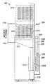
- FIG. 1is a top plan diagrammatic view of a substrate processing system embodying the present invention, with the cover removed from the transport chamber;
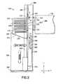
- FIG. 2shows a schematic side view of a substrate station in accordance with the present invention
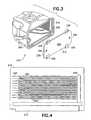
- FIG. 3shows an example embodiment of a magazine
- FIG. 4shows a cross sectional view of a magazine
- FIG. 5is a diagram of an example substrate
- FIGS. 6A and 6Bshow an aperture closure in an extended and retracted position, respectively;
- FIG. 7shows a schematic top view of the substrate station
- FIG. 8shows a schematic side view of the substrate station illustrating a stroke of an elevator
- FIG. 9shows a schematic side view of the substrate station illustrating an operation of a transport apparatus
- FIG. 10shows a schematic side view of the substrate station illustrating an alternate placement of a sensor
- FIG. 11shows another schematic side view of the substrate station illustrating an alternate placement of a sensor and an encoder.
- FIG. 1a perspective view of a system 100 , incorporating features of the present invention, is illustrated.
- a system 100incorporating features of the present invention.
- the present inventionwill be described with reference to the embodiment shown in the drawings, it should be understood that the present invention can be embodied in many alternate forms of embodiments.
- any suitable size, shape or type of elements or materialscould be used.
- the system 100is generally a substrate processing system for processing substrates.
- the substratesmay include 200/300 mm wafers used in semiconductor manufacturing, panels used in the manufacture of flat panel displays, or any other desired type of substrates.
- the substrate processing system 100includes one or more processing modules 105 for performing operations on substrates such as imaging, plasma etching, and the like. It is typical for the processing modules 105 to be arranged about a closed locus as indicated by a dashed line 110 .
- a transport apparatus 115is centrally disposed within a transport chamber 120 for transferring substrates among the one or more of the processing modules 105 .
- Transport chamber 120is preferably maintained substantially at a vacuum to prevent contamination of substrates while they are transported among processing modules 105 . It should be understood that transport chamber 120 may contain any other desired atmosphere for processing substrates.
- the substrate processing system 100preferably includes appropriate systems and plumbing (not shown) for generating, and maintaining the desired atmosphere in transport chamber 120 .
- a vacuum pump(not shown) may be connected to transport chamber 120 using suitable plumbing to draw a desired vacuum condition in transport chamber 120 .
- the vacuum pumpmay be regulated by a controller using appropriate monitoring and control devices (not shown) such as pressure gauges and valves.
- Isolation valves 125are individually provided at the interfaces of the one or more processing modules 105 and the transport chamber 120 .
- Isolation valves 125may comprise slot valves, solenoid valves, hydraulic valves, or any other suitable valves that are capable of being individually opened and closed, and that when closed, form a substantially airtight seal between the transport chamber 120 and the corresponding processing module.
- Each processing module 105may include one or more systems for processing substrates, for example, sputtering, coating, etching, soaking, or any other suitable process for substrates deposited in the respective processing modules.
- Each processing module 105may also include additional isolation valves (not shown) that allow communication with other equipment, or substrate processing by other equipment.
- Transport apparatus 115typically includes a drive section 130 and one or more end effectors 135 .
- Drive section 130may be capable of positioning end effector at any desired XYZ location within transport chamber 120 or may provide limited positioning capabilities, for example, only in the X and Y directions.
- Drive section 130is preferably operable to move end effector 135 along a wafer transfer plane as described in greater detail below.
- the X and Y directionsare horizontal directions and the Z direction is a vertical direction.
- Substrate processing system 100also includes a substrate loading and unloading station, or loadport, referred to herein as a substrate station 140 , in accordance with the present invention.
- Substrate station 140is preferably sealingly positioned in close contact with transport chamber 120 such that transport apparatus 115 may access substrates conveyed by substrate station 140 .
- FIG. 2shows a side view and FIG. 6 shows a top view of the substrate station 140 .
- Substrate station 140has a frame 205 for supporting its components and one or more magazines 210 .
- a magazinewill be understood to include a cassette, a FOUP, or any other substrate carrying device that positions or holds substrates in a spaced arrangement.
- magazine 120is shown as a FOUP for example purposes only.
- FIG. 3shows an example of magazine 120 .
- Magazine 120includes a housing 300 and a magazine opening 310 for providing access to the interior thereof and for receiving a magazine door 315 .
- Magazine door 315 in this exampleincludes a generally rectangular plate 320 with a peripherally extending continuous flange 325 .
- a seal 330is interposed between flange 325 and magazine opening 310 .
- flange 325firmly engages seal 330 to seal the interior of magazine 120 from the surrounding atmosphere.
- a plurality of latch members 335are provided on magazine door 315 at peripherally spaced locations for locking the carrier door 315 in place in magazine opening 310 .
- Latch members 335are movable between an extended, locking position as shown, and a retracted, release position.
- Latch operating mechanisms 340are operably connected to latch members 335 for moving the latch members between the locking position and the release position.
- Latch operating mechanisms 340may be connected by, or may be comprised of, linkages, solenoid devices, or other appropriate apparatus.
- FIG. 4shows a cross sectional view of magazine 210 .
- magazine 210includes a mounting manifold 410 which is suitably mounted on, and projects upwardly from a magazine base 415 .
- a plurality of vertically spaced support plates 420are integral with the mounting manifold 410 and project away from the mounting manifold and lie in equally spaced parallel planes.
- the spacing between the support plates 420may be substantially greater than the thickness of a substrate 425 , and each support plate 420 is preferably adapted to support a substrate 425 on upper surfaces 435 of substrate supports 440 in a generally horizontal plane.
- FIG. 5shows an example of substrate 425 .
- substrate 425may be a silicon planar substrate, a wafer, a flat panel display, or the like.
- Substrate 425may have a peripheral edge 510 with any number of features including a fiducial 515 .
- substrate station 140includes a shield 290 having an aperture 270 for loading and unloading substrates.
- Aperture 270is preferably surrounded by a seal 275 , against which magazine opening 310 may sealingly abut. When magazine opening 310 is in abutting relationship with seal 275 , aperture 270 is aligned with magazine opening 310 .
- Substrate station 140has a magazine door drive 235 , shown in a retracted position, for sealing aperture 270 when magazine opening 310 is not abutting seal 275 , and for coupling to and removing magazine door 315 when magazine opening 310 is abutting seal 275 .
- Magazine door drive 235includes an aperture closure 230 mounted on an extendable member 280 which is operated for both translation and pivoting movement by magazine door drive 235 . When in an extended position, as shown in FIG. 6A , aperture closure 230 seals aperture 270 .
- aperture closureincludes a door transport 285 for operating latch operating mechanism 340 ( FIG.
- Door transport 285includes selectively operable door supports (not shown) which are engageable with magazine door 315 when magazine opening 310 is in abutting relationship with seal 275 .
- Magazine 210 , shield 290 , aperture 270 , and magazine door drive 235are preferably located proximate a central area 265 of substrate station 140 . In alternate embodiments, the area in which magazine 210 , shield 290 , aperture 270 , and magazine door drive 235 are located may not be central.
- Substrate station 140also includes provisions for interfacing to an isolation valve 240 which couples substrate station 140 to transport chamber 120 .
- Isolation valve 240is positioned to allow substrates to be transported along a wafer transfer plane 265 between magazine 210 and transport chamber 120 .
- Substrate station 140additionally includes an elevator 215 for moving magazine 210 in a Z-axis direction.
- Elevator 215may comprise a shelf 237 for supporting magazine 210 , attached to a drive 242 , which may be a ball screw, belt drive, linear motor, or any other suitable device for supporting magazine 210 and providing vertical movement in accordance with the teachings of the invention.
- Elevator 215is operable to precisely move magazine 210 .
- “precisely move”means to repeatably position a substrate 425 held in magazine 210 within a usable range of motion.
- elevator 215is capable of repeatably positioning a substrate held in magazine 210 within at least 0.05 mm.
- Elevator 215is operable to precisely move magazine 210 to position each substrate 425 held in magazine 210 substantially in wafer transfer plane 265 .
- elevator 215is operable to precisely move magazine 210 to position an upper surface 430 of any support plate 420 ( FIG. 4 ), an upper surface 435 of any substrate support 440 ( FIG. 4 ), or other location in the interior of magazine 210 , substantially in wafer transfer plane 265 .
- elevator 215is preferably operable to move magazine 210 to place each substrate 425 held in magazine 210 at any desirable Z axis position.
- elevator 215is preferably operable to move magazine 210 in a way to place each substrate 425 held in magazine 210 at any desirable Z axis position accessible by transport apparatus 115 . Because of the precision placement capabilities of elevator 215 , a transport apparatus may be employed in substrate processing system 100 that has limited or no Z axis capability.
- Substrate station 140also includes a shuttle 220 for moving magazines along the Y-axis, and a buffer transport 225 for moving magazines in an X-axis direction. Substrate station 140 further includes a sensor 245 for mapping substrates and a mini-environment 250 for isolating the interior of magazine 210 from the surrounding atmosphere. Substrate station 140 may be mounted on a carriage 260 allowing substrate station 140 to move in the Y or X direction.
- buffer transport 225is adapted to move the one or more magazines 210 along the X-axis.
- Buffer transport 225may be any suitable mechanism for transporting magazines 210 along the X axis, but is preferably a shelf 610 , guided by a rail 615 aligned with the X axis, coupled to a drive mechanism 620 .
- Buffer transport 225may include a screw, belt, carriage, or any type of driving or movement mechanism.
- substrate station 140includes a plurality of magazines 210 , 210 A, 210 B
- magazines 210 A, 210 Bfunction as one or more substrate buffers, thus enabling the temporary storage or holding of substrates 425 either before or after processing.
- Buffer transport 225is further operable to move individual magazines to and from peripheral areas 650 A, 650 B and into and out of central area 265 .
- Shuttle 220may include any suitable mechanism for transporting magazines 210 along the Y axis.
- Shuttle 220may also comprise a shelf 625 which, in one embodiment, may be shelf 610 . Shelf 625 may guided by a rail 630 along the Y axis, and may be coupled to a suitable drive mechanism 635 .
- shuttle 220operates to move the one or more magazines 210 in a forward Y direction, toward aperture 270 , and in a rearward Y direction, away from aperture 270 .
- Elevator 215is operable to transport one or more magazines 210 vertically in an upward and downward Z direction.
- Shield 290 with aperture 270is operable to move with elevator 215 and magazine 210 such that when magazine opening 310 is sealingly abutting seal 275 , aperture 270 remains aligned with magazine opening 310 during movement of elevator 215 .
- Buffer transport 225 , shuttle 220 , and elevator 215may operate together to position one or more magazines at any location attainable within their combined range of motions.
- Mini-environment 250operates to isolate the interior of magazine 210 from the surrounding atmosphere while magazine 210 abuts seal 275 and magazine door 315 is unlatched and removed.
- Substrate station 140optionally may include devices and mechanisms (not shown) capable of generating and maintaining an environment inside mini-environment 250 having certain characteristics, for example, atmospheric pressure, humidity, presence of certain compounds, etc. The devices and mechanisms may also be operable to match the environment of mini-environment 250 to another environment, for example, the environment of transport chamber 120 .
- isolation valve 240when isolation valve 240 is closed, mini-environment encloses an atmosphere at or slightly above standard atmospheric pressure, and when isolation valve is open, mini-environment encloses an atmosphere at the same pressure as transport chamber 120 .
- Sensor 245 for mapping substratesis preferably mounted to the frame of substrate transport station 140 , inside mini-environment 250 .
- Sensor 245may comprise one or more distance measuring sensors, laser displacement meters, CCD sensors, imaging devices, opto-electronic sensors, capacitive sensors, or any sensor, sensors, or sensor system, suitable for mapping substrates.
- sensor 245is a “through-beam” sensor.
- Sensor 245may be rotated to a retracted position A when not in use and rotated to position B for scanning or mapping operations after magazine opening 310 has been positioned in abutting relationship with seal 275 and magazine door 315 has been removed.
- sensor 245may be retracted in a linear direction C and advanced to position B for scanning.
- sensor 245may be mounted in any orientation at any location so long as sensor 245 is capable of scanning substrates present inside magazine 210 . Elevator 215 may then transport magazine 210 vertically such that substrates 425 within the magazine 210 pass in proximity to sensor 245 , allowing sensor 245 to scan or map substrates 425 .
- sensor 245may record their vertical positions.
- sensor 245may map the horizontal location, and the location of any number of points or features along each substrate's peripheral 510 , including the location of the fiducial 515 ( FIG. 5 ).
- Example operations of substrate station 140are described as follows with reference to FIGS. 2 and 6 - 9 .
- operationsmay begin with aperture closure 230 in an extended position ( FIG. 6A ), effectively sealing aperture 270 .
- Buffer transport 225then operates to move a magazine 210 with a locked magazine door 315 along the X-axis from peripheral area 650 A or 650 B into central area 265 .
- Shuttle 220then operates to move magazine 210 in a forward Y direction until magazine opening 310 sealingly abuts seal 275 .
- Magazine door drive 235then operates aperture closure 230 so that door supports 295 on door transport 285 engage magazine door 315 . Once door supports 295 have engaged magazine door 315 , door transport 285 operates latch operating mechanism 340 to release magazine door 315 from magazine 210 . Magazine door drive 235 then operates member 280 to remove magazine door 315 from magazine 215 and transport magazine door 315 to a lowered position, away from magazine opening 310 ( FIG. 6B ).
- U.S. Pat. No. 6,071,059incorporated by reference in its entirety, describes a typical door removal operation.
- Sensor 245then rotates to position B.
- Sensor 245may be actuated directly or indirectly by the action of removing magazine door 315 , or may be actuated independently.
- Isolation valve 240may be opened simultaneously with the removal of magazine door 315 , or may be opened at a later time.
- Elevator 215then vertically moves magazine 210 such that all substrates 425 are transported past sensor 245 .
- elevator 215is at least capable of moving shelf 237 from a lower position 710 to an upper position 715 .
- the vertical position of each substrate 245is mapped as it passes sensor 245 . After mapping is complete, sensor 245 may be returned to retracted position B.
- elevator 215then returns magazine 210 to a known height in central area 265 , positioning a particular substrate 425 in wafer transfer plane 265 , which is a plane that is accessible by transport apparatus 115 .
- Isolation valve 240may be opened at this time if not previously opened.
- Transport apparatus 115may then extend end effector 135 into magazine 210 to remove substrate 425 . Because the substrates have been mapped by sensor 245 , the location of each substrate 425 is known and elevator 215 may subsequently move magazine 210 such that a particular substrate is positioned in wafer transfer plane 265 for removal by transport apparatus 115 without any significant Z-axis movement by transport apparatus 115 .
- Transport apparatus 115may then replace substrates 425 in magazine 210 in a similar fashion, where elevator 215 moves magazine 210 such a that a particular support plate 420 ( FIG. 4 ) of magazine 210 is situated adjacent wafer transfer plane 265 , allowing transport apparatus 115 to replace a previously removed substrate or to place another substrate in magazine 210 .
- Substrate station 140may coordinate the movements of elevator 215 with the movements of transport apparatus 115 such that substrates 425 may be removed from or placed into magazine 210 in any desirable order or location.
- Transport apparatus 115retracts end effector 135 and isolation valve 240 may be closed while magazine door drive 235 replaces and locks magazine door 315 .
- the action of replacing magazine door 315may cause sensor 245 to move to retracted position B.
- shuttle 220may then operate to move magazine 210 in a rearward Y direction, causing magazine opening 310 to disengage from seal 275 .
- Buffer transport 225may then move magazine 210 to one of the peripheral areas for example, 650 B ( FIG. 6 ), and then move magazine 210 A from peripheral area 650 A to central area 265 for processing the substrates therein.
- buffer transportis capable of moving any one of the magazines among peripheral areas 650 A, 650 B, and central area 265 as required for loading, unloading, and processing of substrates.
- FIG. 10shows another embodiment of the invention where sensor 245 is part of magazine door drive 235 .
- magazine door drive 235additionally operates to place sensor 245 in position for mapping substrates 425 inside magazine 210 .
- Sensor 245may be mounted to member 280 , for example, by way of a bracket 1020 and may extend above, to the side, or below aperture closure 230 . Alternately, sensor 245 may be mounted on aperture closure 230 or member 280 . In other embodiments, sensor 245 may be mounted directly or indirectly to magazine door drive 235 utilizing any arrangement, so long as magazine door drive 235 is capable of placing sensor 245 in a mapping position.
- Exemplary mapping operations utilizing this embodimentmay begin with aperture closure 230 in an extended position ( FIG. 6A ), to seal or cover aperture 270 .
- Shuttle 220FIG. 2
- Magazine door drive 235then operates to engage magazine door 315 , operate latch operating mechanism 340 to release and remove magazine door 315 from magazine 210 as described above, transport magazine door 315 through aperture 270 to a lowered position, away from magazine opening 310 ( FIG. 6B ).
- Magazine door drive 235may then operate to position sensor 245 in view of substrates 425 .
- sensor 245may be positioned and magazine door drive may operate such that magazine door drive 235 may position sensor 245 for mapping without moving magazine door 315 to a lowered position, or without moving magazine door 315 away from magazine opening 310 .
- elevator 215vertically moves magazine 210 such that all substrates 425 are transported past sensor 245 .
- the vertical position of each substrate 245is mapped as it passes sensor 245 .
- elevator 215may move vertically and mapping may occur simultaneously with the release and removal of magazine door 315 from magazine 210 . After mapping is complete, elevator 215 may return to a rest position and magazine door drive 235 may re-engage magazine door 315 with magazine 210 .
- magazine door drive 235may be a fluidic drive, for example, a pneumatic drive.
- elevator 215 or elevator drive 242may be equipped with an encoder 1000 which provides elevator position information.
- Encoder 1000may be any type of encoder capable of providing information regarding the vertical position of the elevator.
- encoder 1000may be an optical encoder that may operate to read a scale 1010 to determine position information.
- Optical encoder 1000 and sensor 245may be operated together to map substrates 425 . For example, after sensor 245 has been placed in mapping position by magazine door drive 235 , an output of sensor 245 may be monitored while elevator 215 moves magazine 210 from lower position 710 to upper position 715 . As sensor 245 detects an individual substrate, the position of elevator 215 as reported by encoder 1000 may be recorded. These positions may then be translated to substrate positions, for example, by using known dimensions of system 100 .
- FIG. 11shows yet another embodiment of the invention where sensor 245 is part of magazine door drive 234 and encoder 1000 may also be a part of magazine door drive 235 .
- Encoder 1000may be any type of encoder capable of providing information regarding the position of the magazine door drive 235 , and may be located anywhere within system 100 .
- encoder 1000may be an optical encoder that may operate to read a scale 1010 to determine position information.
- An exemplary mapping operationmay be performed by operating magazine door drive 235 while monitoring an output of encoder 1000 and an output of sensor 245 .
- the position of magazine door drive 235 as reported by encoder 1000may be processed with the output of sensor 245 to determine substrate positions.
- substrate station 140is capable of holding a buffer of substrates 425 for processing, disposition after processing, or storage.
- Sensor 245is capable of mapping the location and features of substrates 425 while situated near magazine 210 , preferably positioned in central area 265 .
- Buffer transport 225 , shuttle 220 , and elevator 215are capable of operating together to position one or more magazines 210 , and thus the substrates therein, at any position within their combined range of motions.
- One advantage of these mapping and positioning capabilitiesis the ability to place each substrate at the wafer transfer plane 265 , eliminating the need for any significant Z-axis movement by transport apparatus 115 .
- Substrate station 140is capable of being mated directly to transport chamber 120 , thus eliminating the need for a front end for substrate alignment and placement.
Landscapes
- Engineering & Computer Science (AREA)
- Physics & Mathematics (AREA)
- Condensed Matter Physics & Semiconductors (AREA)
- General Physics & Mathematics (AREA)
- Manufacturing & Machinery (AREA)
- Computer Hardware Design (AREA)
- Microelectronics & Electronic Packaging (AREA)
- Power Engineering (AREA)
- Container, Conveyance, Adherence, Positioning, Of Wafer (AREA)
- Drying Of Semiconductors (AREA)
- Cleaning Or Drying Semiconductors (AREA)
Abstract
Description
Claims (9)
Priority Applications (2)
| Application Number | Priority Date | Filing Date | Title |
|---|---|---|---|
| US12/723,837US8454293B2 (en) | 2002-07-22 | 2010-03-15 | Substrate loading and unloading station with buffer |
| US13/908,909US9670010B2 (en) | 2002-07-22 | 2013-06-03 | Substrate loading and unloading station with buffer |
Applications Claiming Priority (3)
| Application Number | Priority Date | Filing Date | Title |
|---|---|---|---|
| US10/200,818US6869263B2 (en) | 2002-07-22 | 2002-07-22 | Substrate loading and unloading station with buffer |
| US10/623,970US7677859B2 (en) | 2002-07-22 | 2003-07-21 | Substrate loading and uploading station with buffer |
| US12/723,837US8454293B2 (en) | 2002-07-22 | 2010-03-15 | Substrate loading and unloading station with buffer |
Related Parent Applications (1)
| Application Number | Title | Priority Date | Filing Date |
|---|---|---|---|
| US10/623,970ContinuationUS7677859B2 (en) | 2002-07-22 | 2003-07-21 | Substrate loading and uploading station with buffer |
Related Child Applications (1)
| Application Number | Title | Priority Date | Filing Date |
|---|---|---|---|
| US13/908,909ContinuationUS9670010B2 (en) | 2002-07-22 | 2013-06-03 | Substrate loading and unloading station with buffer |
Publications (2)
| Publication Number | Publication Date |
|---|---|
| US20100172721A1 US20100172721A1 (en) | 2010-07-08 |
| US8454293B2true US8454293B2 (en) | 2013-06-04 |
Family
ID=30772537
Family Applications (3)
| Application Number | Title | Priority Date | Filing Date |
|---|---|---|---|
| US10/623,970Expired - LifetimeUS7677859B2 (en) | 2002-07-22 | 2003-07-21 | Substrate loading and uploading station with buffer |
| US12/723,837Expired - Fee RelatedUS8454293B2 (en) | 2002-07-22 | 2010-03-15 | Substrate loading and unloading station with buffer |
| US13/908,909Expired - Fee RelatedUS9670010B2 (en) | 2002-07-22 | 2013-06-03 | Substrate loading and unloading station with buffer |
Family Applications Before (1)
| Application Number | Title | Priority Date | Filing Date |
|---|---|---|---|
| US10/623,970Expired - LifetimeUS7677859B2 (en) | 2002-07-22 | 2003-07-21 | Substrate loading and uploading station with buffer |
Family Applications After (1)
| Application Number | Title | Priority Date | Filing Date |
|---|---|---|---|
| US13/908,909Expired - Fee RelatedUS9670010B2 (en) | 2002-07-22 | 2013-06-03 | Substrate loading and unloading station with buffer |
Country Status (4)
| Country | Link |
|---|---|
| US (3) | US7677859B2 (en) |
| JP (1) | JP4542893B2 (en) |
| AU (1) | AU2003254103A1 (en) |
| WO (1) | WO2004009862A2 (en) |
Cited By (3)
| Publication number | Priority date | Publication date | Assignee | Title |
|---|---|---|---|---|
| US20150032262A1 (en)* | 2013-03-01 | 2015-01-29 | Boe Technology Group Co., Ltd. | Apparatus for identifying layer number of an object in a container and system for automatically taking out an object |
| US10092929B2 (en)* | 2013-03-14 | 2018-10-09 | Brooks Automation, Inc. | Wafer tray sorter with door coupled to detector |
| US11072502B2 (en)* | 2018-05-03 | 2021-07-27 | Applied Materials, Inc. | Substrate tilt control in high speed rotary sorter |
Families Citing this family (19)
| Publication number | Priority date | Publication date | Assignee | Title |
|---|---|---|---|---|
| KR100999104B1 (en)* | 2003-10-01 | 2010-12-07 | 삼성전자주식회사 | Board conveying device |
| WO2007061603A2 (en)* | 2005-11-21 | 2007-05-31 | Applied Materials, Inc. | Methods and apparatus for transferring substrates during electronic device manufacturing |
| TWD119731S1 (en)* | 2006-03-30 | 2007-11-01 | 東京威力科創股份有限公司 | Wafer carrying-in/out apparatus |
| DE102006019785B4 (en)* | 2006-04-28 | 2009-01-08 | Mühlbauer Ag | Apparatus and method for sequentially transporting a plurality of GSM smart cards |
| AU2007298929B2 (en) | 2006-09-21 | 2012-09-27 | Probiodrug Ag | Novel genes related to glutaminyl cyclase |
| US20100028111A1 (en)* | 2008-07-31 | 2010-02-04 | Asyst Technologies, Inc. | Variable-Size Load Port and Method for Operating the Same |
| US8919756B2 (en) | 2008-08-28 | 2014-12-30 | Tokyo Ohka Kogyo Co., Ltd. | Substrate processing system, carrying device, and coating device |
| US9214372B2 (en)* | 2008-08-28 | 2015-12-15 | Tokyo Ohka Kogyo Co., Ltd. | Substrate processing system, carrying device and coating device |
| JP5768337B2 (en)* | 2010-07-07 | 2015-08-26 | シンフォニアテクノロジー株式会社 | Load port |
| JP2012051093A (en)* | 2010-09-03 | 2012-03-15 | Disco Corp | Machining apparatus |
| JP2013143425A (en)* | 2012-01-10 | 2013-07-22 | Tokyo Electron Ltd | Substrate processing system and substrate position correction method |
| US9337014B1 (en) | 2012-03-09 | 2016-05-10 | Alta Devices, Inc. | Processing system architecture with single load lock chamber |
| JP6114060B2 (en)* | 2013-02-27 | 2017-04-12 | 東京エレクトロン株式会社 | Substrate transport apparatus, substrate delivery position confirmation method, and substrate processing system |
| TWI684229B (en) | 2013-07-08 | 2020-02-01 | 美商布魯克斯自動機械公司 | Process apparatus with on-the-fly substrate centering |
| US20170252991A1 (en)* | 2016-03-03 | 2017-09-07 | Juicero, Inc. | Juicer with flexible seal |
| CN106409728B (en)* | 2016-10-31 | 2019-02-19 | 北京北方华创微电子装备有限公司 | A kind of sealing structure and a kind of semiconductor equipment |
| CN108346605B (en)* | 2017-01-23 | 2019-08-06 | 孙建忠 | Substrate storage and delivery system |
| JP7238126B2 (en)* | 2019-06-27 | 2023-03-13 | 川崎重工業株式会社 | Substrate mapping device, its mapping method, and mapping teaching method |
| US12237192B2 (en) | 2020-04-17 | 2025-02-25 | Kla Corporation | Mini-environment system for controlling oxygen and humidity levels within a sample transport device |
Citations (64)
| Publication number | Priority date | Publication date | Assignee | Title |
|---|---|---|---|---|
| US4674939A (en) | 1984-07-30 | 1987-06-23 | Asyst Technologies | Sealed standard interface apparatus |
| US4676709A (en) | 1985-08-26 | 1987-06-30 | Asyst Technologies | Long arm manipulator for standard mechanical interface apparatus |
| JPS62258881A (en) | 1986-05-06 | 1987-11-11 | Mitsubishi Heavy Ind Ltd | Automatic lock device |
| US4758127A (en) | 1983-06-24 | 1988-07-19 | Canon Kabushiki Kaisha | Original feeding apparatus and a cassette for containing the original |
| US4836733A (en) | 1986-04-28 | 1989-06-06 | Varian Associates, Inc. | Wafer transfer system |
| JPH01284439A (en) | 1988-05-12 | 1989-11-15 | Murata Mach Ltd | Positioning device for plate material |
| JPH01291442A (en) | 1988-05-19 | 1989-11-24 | Hitachi Kiden Kogyo Ltd | Transfer apparatus in step of processing |
| JPH01310686A (en) | 1988-03-24 | 1989-12-14 | Artur Fischer Gmbh | Toy assembling block equipped with connection pin |
| US4895486A (en) | 1987-05-15 | 1990-01-23 | Roboptek, Inc. | Wafer monitoring device |
| JPH0269955A (en) | 1988-09-06 | 1990-03-08 | Canon Inc | Mask loading mechanism |
| US4917556A (en) | 1986-04-28 | 1990-04-17 | Varian Associates, Inc. | Modular wafer transport and processing system |
| US4995430A (en) | 1989-05-19 | 1991-02-26 | Asyst Technologies, Inc. | Sealable transportable container having improved latch mechanism |
| EP0452939A1 (en) | 1990-04-19 | 1991-10-23 | Applied Materials, Inc. | Apparatus and method for loading workpieces in a processing system |
| JPH03261161A (en) | 1990-03-09 | 1991-11-21 | Tokyo Electron Sagami Ltd | Vertical heat treating method |
| JPH0479347A (en) | 1990-07-23 | 1992-03-12 | Seiko Epson Corp | wafer carrier |
| JPH0485813A (en) | 1990-07-26 | 1992-03-18 | Seiko Epson Corp | Vacuum treatment equipment |
| JPH04206547A (en) | 1990-11-30 | 1992-07-28 | Hitachi Ltd | Transfer method between devices |
| US5139459A (en) | 1990-10-22 | 1992-08-18 | Tdk Corporation | Clean transfer method and system therefor |
| JPH04302454A (en) | 1991-03-29 | 1992-10-26 | Mitsubishi Electric Corp | semiconductor manufacturing equipment |
| JPH04360545A (en) | 1991-06-07 | 1992-12-14 | Sharp Corp | parts supply device |
| JPH05338728A (en) | 1992-06-05 | 1993-12-21 | Fujitsu Ltd | Wafer transfer method and device |
| EP0574893A2 (en) | 1992-06-19 | 1993-12-22 | International Business Machines Corporation | Method of printed circuit panel manufacture |
| JPH0632449A (en) | 1992-05-19 | 1994-02-08 | Ebara Corp | Wafer carrying and storing system in manufacturing processing for semiconductor |
| US5291923A (en) | 1992-09-24 | 1994-03-08 | Internatinal Business Machines Corporation | Door opening system and method |
| FR2696429A1 (en) | 1992-10-06 | 1994-04-08 | Shinko Electic Co Ltd | Automatic material transferring system using closed portable carrier - collects material from processing station for delivery to another in sealed carrier on automatic guided vehicle |
| JPH06151266A (en) | 1992-06-19 | 1994-05-31 | Internatl Business Mach Corp <Ibm> | Air-lock transfer port and reduced-contamination manufacturing system |
| JPH06211311A (en) | 1993-01-19 | 1994-08-02 | Hioki Ee Corp | Magazine rack supply device of circuit board inspection machine |
| JPH06302679A (en) | 1993-04-13 | 1994-10-28 | Tokyo Electron Ltd | Material-to-be-treated conveying box and treating apparatus |
| US5380682A (en) | 1991-05-17 | 1995-01-10 | Materials Research Corporation | Wafer processing cluster tool batch preheating and degassing method |
| US5387265A (en) | 1991-10-29 | 1995-02-07 | Kokusai Electric Co., Ltd. | Semiconductor wafer reaction furnace with wafer transfer means |
| US5388944A (en) | 1992-02-07 | 1995-02-14 | Tokyo Electron Tohoku Kabushiki Kaisha | Vertical heat-treating apparatus and heat-treating process by using the vertical heat-treating apparatus |
| US5407350A (en) | 1992-02-13 | 1995-04-18 | Tokyo Electron Limited | Heat-treatment apparatus |
| US5418382A (en) | 1993-09-23 | 1995-05-23 | Fsi International, Inc. | Substrate location and detection apparatus |
| US5509772A (en) | 1992-01-16 | 1996-04-23 | Commissariat A L'energie Atomique | System for the handling and confinement of flat objects in individual boxes |
| US5540098A (en) | 1993-02-16 | 1996-07-30 | Tokyo Electron Limited | Transfer device |
| US5551830A (en) | 1993-06-30 | 1996-09-03 | Mitsubishi Denki Kabushiki Kaisha | Automatic lot organization method |
| JPH08279546A (en) | 1995-03-28 | 1996-10-22 | Jenoptik Ag | Loading and unloading station for semiconductor processing equipment |
| US5570990A (en) | 1993-11-05 | 1996-11-05 | Asyst Technologies, Inc. | Human guided mobile loader stocker |
| US5605428A (en) | 1993-03-05 | 1997-02-25 | Jenoptik Gmbh | Device for indexing magazine compartments and wafer-shaped objects in the compartments |
| US5788447A (en) | 1995-08-05 | 1998-08-04 | Kokusai Electric Co., Ltd. | Substrate processing apparatus |
| US5857848A (en) | 1996-09-13 | 1999-01-12 | Tokyo Electron Limited | Transfer apparatus and vertical heat-processing system using the same |
| US5882165A (en)* | 1986-12-19 | 1999-03-16 | Applied Materials, Inc. | Multiple chamber integrated process system |
| US5906469A (en)* | 1995-11-22 | 1999-05-25 | Dainippon Screen Mfg. Co., Ltd. | Apparatus and method for detecting and conveying substrates in cassette |
| US5980183A (en) | 1997-04-14 | 1999-11-09 | Asyst Technologies, Inc. | Integrated intrabay buffer, delivery, and stocker system |
| US6013920A (en)* | 1997-11-28 | 2000-01-11 | Fortrend Engineering Coirporation | Wafer-mapping load post interface having an effector position sensing device |
| JP2000188320A (en) | 1998-12-24 | 2000-07-04 | Hitachi Ltd | Local clean system |
| US6135698A (en)* | 1999-04-30 | 2000-10-24 | Asyst Technologies, Inc. | Universal tool interface and/or workpiece transfer apparatus for SMIF and open pod applications |
| US6183186B1 (en) | 1997-08-29 | 2001-02-06 | Daitron, Inc. | Wafer handling system and method |
| US6188323B1 (en) | 1998-10-15 | 2001-02-13 | Asyst Technologies, Inc. | Wafer mapping system |
| US6281516B1 (en) | 1998-07-13 | 2001-08-28 | Newport Corporation | FIMS transport box load interface |
| JP2001250853A (en) | 2000-03-03 | 2001-09-14 | Canon Inc | Substrate transfer device, substrate transfer method, container supply device, semiconductor manufacturing device, and semiconductor device production method |
| US6318945B1 (en) | 1999-07-28 | 2001-11-20 | Brooks Automation, Inc. | Substrate processing apparatus with vertically stacked load lock and substrate transport robot |
| JP2002009131A (en) | 2000-04-17 | 2002-01-11 | Hitachi Kokusai Electric Inc | Substrate processing apparatus, substrate processing method, and semiconductor device manufacturing method |
| JP3261161B2 (en) | 1992-06-23 | 2002-02-25 | 株式会社日立製作所 | Method of manufacturing thin-film magnetic disk |
| US6410455B1 (en) | 1999-11-30 | 2002-06-25 | Wafermasters, Inc. | Wafer processing system |
| US6452201B1 (en) | 2000-07-13 | 2002-09-17 | Industrial Technology Research Institute | Wafer-mapping method of wafer load port equipment |
| US6501070B1 (en) | 1998-07-13 | 2002-12-31 | Newport Corporation | Pod load interface equipment adapted for implementation in a fims system |
| US6506009B1 (en)* | 2000-03-16 | 2003-01-14 | Applied Materials, Inc. | Apparatus for storing and moving a cassette |
| JP2003215002A (en) | 2002-01-17 | 2003-07-30 | Dainippon Screen Mfg Co Ltd | Apparatus and method for treating board |
| JP4079347B2 (en) | 2002-03-11 | 2008-04-23 | 株式会社フジタ | Power generator |
| JP4085813B2 (en) | 2000-12-28 | 2008-05-14 | 株式会社ニコン | Exposure equipment |
| JP4206547B2 (en) | 1999-02-23 | 2009-01-14 | 株式会社セガ | Image processing method, image processing apparatus, integrated shaping model data used therefor, and recording medium on which image processing program is recorded |
| JP4302454B2 (en) | 2003-07-16 | 2009-07-29 | 富士通テン株式会社 | Self-excited oscillation type load drive device and load control circuit |
| JP4360545B2 (en) | 2004-07-14 | 2009-11-11 | 光洋サーモシステム株式会社 | Continuous heat treatment furnace |
Family Cites Families (5)
| Publication number | Priority date | Publication date | Assignee | Title |
|---|---|---|---|---|
| JPS63252439A (en)* | 1986-12-19 | 1988-10-19 | アプライド マテリアルズインコーポレーテッド | Multi-chamber integrated processing system |
| JP2003515878A (en)* | 1999-11-24 | 2003-05-07 | コーニンクレッカ フィリップス エレクトロニクス エヌ ヴィ | Voltage divider, an electron gun provided with the voltage divider, and a cathode ray tube provided with the electron gun |
| JP2001284439A (en) | 2000-03-30 | 2001-10-12 | Tdk Corp | Wafer mapping device |
| JP5338728B2 (en) | 2010-03-26 | 2013-11-13 | ブラザー工業株式会社 | Management system, management server, portable terminal, server program, and terminal program |
| JP6032449B1 (en) | 2015-11-17 | 2016-11-30 | 恭徳 野々市 | Cyber attack email response training system |
- 2003
- 2003-07-21USUS10/623,970patent/US7677859B2/ennot_activeExpired - Lifetime
- 2003-07-22WOPCT/US2003/022880patent/WO2004009862A2/enactiveApplication Filing
- 2003-07-22AUAU2003254103Apatent/AU2003254103A1/ennot_activeAbandoned
- 2003-07-22JPJP2004523279Apatent/JP4542893B2/ennot_activeExpired - Lifetime
- 2010
- 2010-03-15USUS12/723,837patent/US8454293B2/ennot_activeExpired - Fee Related
- 2013
- 2013-06-03USUS13/908,909patent/US9670010B2/ennot_activeExpired - Fee Related
Patent Citations (68)
| Publication number | Priority date | Publication date | Assignee | Title |
|---|---|---|---|---|
| US4758127A (en) | 1983-06-24 | 1988-07-19 | Canon Kabushiki Kaisha | Original feeding apparatus and a cassette for containing the original |
| US4674939A (en) | 1984-07-30 | 1987-06-23 | Asyst Technologies | Sealed standard interface apparatus |
| US4676709A (en) | 1985-08-26 | 1987-06-30 | Asyst Technologies | Long arm manipulator for standard mechanical interface apparatus |
| US4836733A (en) | 1986-04-28 | 1989-06-06 | Varian Associates, Inc. | Wafer transfer system |
| US4917556A (en) | 1986-04-28 | 1990-04-17 | Varian Associates, Inc. | Modular wafer transport and processing system |
| JPS62258881A (en) | 1986-05-06 | 1987-11-11 | Mitsubishi Heavy Ind Ltd | Automatic lock device |
| US5882165A (en)* | 1986-12-19 | 1999-03-16 | Applied Materials, Inc. | Multiple chamber integrated process system |
| US4895486A (en) | 1987-05-15 | 1990-01-23 | Roboptek, Inc. | Wafer monitoring device |
| JPH01310686A (en) | 1988-03-24 | 1989-12-14 | Artur Fischer Gmbh | Toy assembling block equipped with connection pin |
| JPH01284439A (en) | 1988-05-12 | 1989-11-15 | Murata Mach Ltd | Positioning device for plate material |
| JPH01291442A (en) | 1988-05-19 | 1989-11-24 | Hitachi Kiden Kogyo Ltd | Transfer apparatus in step of processing |
| JPH0269955A (en) | 1988-09-06 | 1990-03-08 | Canon Inc | Mask loading mechanism |
| US4995430A (en) | 1989-05-19 | 1991-02-26 | Asyst Technologies, Inc. | Sealable transportable container having improved latch mechanism |
| JPH03261161A (en) | 1990-03-09 | 1991-11-21 | Tokyo Electron Sagami Ltd | Vertical heat treating method |
| EP0452939A1 (en) | 1990-04-19 | 1991-10-23 | Applied Materials, Inc. | Apparatus and method for loading workpieces in a processing system |
| JPH0479347A (en) | 1990-07-23 | 1992-03-12 | Seiko Epson Corp | wafer carrier |
| JPH0485813A (en) | 1990-07-26 | 1992-03-18 | Seiko Epson Corp | Vacuum treatment equipment |
| US5139459A (en) | 1990-10-22 | 1992-08-18 | Tdk Corporation | Clean transfer method and system therefor |
| JPH04206547A (en) | 1990-11-30 | 1992-07-28 | Hitachi Ltd | Transfer method between devices |
| JPH04302454A (en) | 1991-03-29 | 1992-10-26 | Mitsubishi Electric Corp | semiconductor manufacturing equipment |
| US5380682A (en) | 1991-05-17 | 1995-01-10 | Materials Research Corporation | Wafer processing cluster tool batch preheating and degassing method |
| JPH04360545A (en) | 1991-06-07 | 1992-12-14 | Sharp Corp | parts supply device |
| US5387265A (en) | 1991-10-29 | 1995-02-07 | Kokusai Electric Co., Ltd. | Semiconductor wafer reaction furnace with wafer transfer means |
| US5509772A (en) | 1992-01-16 | 1996-04-23 | Commissariat A L'energie Atomique | System for the handling and confinement of flat objects in individual boxes |
| US5388944A (en) | 1992-02-07 | 1995-02-14 | Tokyo Electron Tohoku Kabushiki Kaisha | Vertical heat-treating apparatus and heat-treating process by using the vertical heat-treating apparatus |
| US5407350A (en) | 1992-02-13 | 1995-04-18 | Tokyo Electron Limited | Heat-treatment apparatus |
| JPH0632449A (en) | 1992-05-19 | 1994-02-08 | Ebara Corp | Wafer carrying and storing system in manufacturing processing for semiconductor |
| JPH05338728A (en) | 1992-06-05 | 1993-12-21 | Fujitsu Ltd | Wafer transfer method and device |
| JPH06151266A (en) | 1992-06-19 | 1994-05-31 | Internatl Business Mach Corp <Ibm> | Air-lock transfer port and reduced-contamination manufacturing system |
| EP0574893A2 (en) | 1992-06-19 | 1993-12-22 | International Business Machines Corporation | Method of printed circuit panel manufacture |
| JP3261161B2 (en) | 1992-06-23 | 2002-02-25 | 株式会社日立製作所 | Method of manufacturing thin-film magnetic disk |
| US5291923A (en) | 1992-09-24 | 1994-03-08 | Internatinal Business Machines Corporation | Door opening system and method |
| US5431600A (en) | 1992-10-06 | 1995-07-11 | Shinko Electric Co., Ltd. | Automatic transferring system using portable closed container |
| FR2696429A1 (en) | 1992-10-06 | 1994-04-08 | Shinko Electic Co Ltd | Automatic material transferring system using closed portable carrier - collects material from processing station for delivery to another in sealed carrier on automatic guided vehicle |
| JPH06211311A (en) | 1993-01-19 | 1994-08-02 | Hioki Ee Corp | Magazine rack supply device of circuit board inspection machine |
| US5540098A (en) | 1993-02-16 | 1996-07-30 | Tokyo Electron Limited | Transfer device |
| US5605428A (en) | 1993-03-05 | 1997-02-25 | Jenoptik Gmbh | Device for indexing magazine compartments and wafer-shaped objects in the compartments |
| JPH06302679A (en) | 1993-04-13 | 1994-10-28 | Tokyo Electron Ltd | Material-to-be-treated conveying box and treating apparatus |
| US6012894A (en) | 1993-06-30 | 2000-01-11 | Mitsubishi Denki Kabushiki Kaisha | Automatic lot organization method |
| US5551830A (en) | 1993-06-30 | 1996-09-03 | Mitsubishi Denki Kabushiki Kaisha | Automatic lot organization method |
| US5418382A (en) | 1993-09-23 | 1995-05-23 | Fsi International, Inc. | Substrate location and detection apparatus |
| US5570990A (en) | 1993-11-05 | 1996-11-05 | Asyst Technologies, Inc. | Human guided mobile loader stocker |
| JPH08279546A (en) | 1995-03-28 | 1996-10-22 | Jenoptik Ag | Loading and unloading station for semiconductor processing equipment |
| US5772386A (en)* | 1995-03-28 | 1998-06-30 | Jenoptik Ag | Loading and unloading station for semiconductor processing installations |
| US6071059A (en) | 1995-03-28 | 2000-06-06 | Brooks Automation Gmbh | Loading and unloading station for semiconductor processing installations |
| US5788447A (en) | 1995-08-05 | 1998-08-04 | Kokusai Electric Co., Ltd. | Substrate processing apparatus |
| US5906469A (en)* | 1995-11-22 | 1999-05-25 | Dainippon Screen Mfg. Co., Ltd. | Apparatus and method for detecting and conveying substrates in cassette |
| US5857848A (en) | 1996-09-13 | 1999-01-12 | Tokyo Electron Limited | Transfer apparatus and vertical heat-processing system using the same |
| US5980183A (en) | 1997-04-14 | 1999-11-09 | Asyst Technologies, Inc. | Integrated intrabay buffer, delivery, and stocker system |
| US6183186B1 (en) | 1997-08-29 | 2001-02-06 | Daitron, Inc. | Wafer handling system and method |
| US6013920A (en)* | 1997-11-28 | 2000-01-11 | Fortrend Engineering Coirporation | Wafer-mapping load post interface having an effector position sensing device |
| US6501070B1 (en) | 1998-07-13 | 2002-12-31 | Newport Corporation | Pod load interface equipment adapted for implementation in a fims system |
| US6281516B1 (en) | 1998-07-13 | 2001-08-28 | Newport Corporation | FIMS transport box load interface |
| US6188323B1 (en) | 1998-10-15 | 2001-02-13 | Asyst Technologies, Inc. | Wafer mapping system |
| JP2000188320A (en) | 1998-12-24 | 2000-07-04 | Hitachi Ltd | Local clean system |
| JP4206547B2 (en) | 1999-02-23 | 2009-01-14 | 株式会社セガ | Image processing method, image processing apparatus, integrated shaping model data used therefor, and recording medium on which image processing program is recorded |
| US6135698A (en)* | 1999-04-30 | 2000-10-24 | Asyst Technologies, Inc. | Universal tool interface and/or workpiece transfer apparatus for SMIF and open pod applications |
| US6318945B1 (en) | 1999-07-28 | 2001-11-20 | Brooks Automation, Inc. | Substrate processing apparatus with vertically stacked load lock and substrate transport robot |
| US6410455B1 (en) | 1999-11-30 | 2002-06-25 | Wafermasters, Inc. | Wafer processing system |
| JP2001250853A (en) | 2000-03-03 | 2001-09-14 | Canon Inc | Substrate transfer device, substrate transfer method, container supply device, semiconductor manufacturing device, and semiconductor device production method |
| US6506009B1 (en)* | 2000-03-16 | 2003-01-14 | Applied Materials, Inc. | Apparatus for storing and moving a cassette |
| JP2002009131A (en) | 2000-04-17 | 2002-01-11 | Hitachi Kokusai Electric Inc | Substrate processing apparatus, substrate processing method, and semiconductor device manufacturing method |
| US6452201B1 (en) | 2000-07-13 | 2002-09-17 | Industrial Technology Research Institute | Wafer-mapping method of wafer load port equipment |
| JP4085813B2 (en) | 2000-12-28 | 2008-05-14 | 株式会社ニコン | Exposure equipment |
| JP2003215002A (en) | 2002-01-17 | 2003-07-30 | Dainippon Screen Mfg Co Ltd | Apparatus and method for treating board |
| JP4079347B2 (en) | 2002-03-11 | 2008-04-23 | 株式会社フジタ | Power generator |
| JP4302454B2 (en) | 2003-07-16 | 2009-07-29 | 富士通テン株式会社 | Self-excited oscillation type load drive device and load control circuit |
| JP4360545B2 (en) | 2004-07-14 | 2009-11-11 | 光洋サーモシステム株式会社 | Continuous heat treatment furnace |
Cited By (4)
| Publication number | Priority date | Publication date | Assignee | Title |
|---|---|---|---|---|
| US20150032262A1 (en)* | 2013-03-01 | 2015-01-29 | Boe Technology Group Co., Ltd. | Apparatus for identifying layer number of an object in a container and system for automatically taking out an object |
| US9481090B2 (en)* | 2013-03-01 | 2016-11-01 | Boe Technology Group Co., Ltd. | Apparatus for identifying layer number of an object in a container and system for automatically taking out an object |
| US10092929B2 (en)* | 2013-03-14 | 2018-10-09 | Brooks Automation, Inc. | Wafer tray sorter with door coupled to detector |
| US11072502B2 (en)* | 2018-05-03 | 2021-07-27 | Applied Materials, Inc. | Substrate tilt control in high speed rotary sorter |
Also Published As
| Publication number | Publication date |
|---|---|
| AU2003254103A1 (en) | 2004-02-09 |
| US20040141831A1 (en) | 2004-07-22 |
| WO2004009862A2 (en) | 2004-01-29 |
| JP2005534175A (en) | 2005-11-10 |
| US20130336749A1 (en) | 2013-12-19 |
| US9670010B2 (en) | 2017-06-06 |
| US7677859B2 (en) | 2010-03-16 |
| US20100172721A1 (en) | 2010-07-08 |
| AU2003254103A8 (en) | 2004-02-09 |
| JP4542893B2 (en) | 2010-09-15 |
| WO2004009862A3 (en) | 2004-03-18 |
Similar Documents
| Publication | Publication Date | Title |
|---|---|---|
| US8454293B2 (en) | Substrate loading and unloading station with buffer | |
| US6869263B2 (en) | Substrate loading and unloading station with buffer | |
| US11658051B2 (en) | Substrate transport | |
| US11201070B2 (en) | Side opening unified pod | |
| TW591736B (en) | Integrated system for tool front-end workpiece handling | |
| US11664259B2 (en) | Process apparatus with on-the-fly substrate centering | |
| TW579538B (en) | Wafer engine | |
| US7100340B2 (en) | Unified frame for semiconductor material handling system | |
| US20030044261A1 (en) | Semiconductor material handling system | |
| WO2001094245A1 (en) | Material transport system | |
| WO2000044653A1 (en) | Substrate carrier as batchloader | |
| KR20100020968A (en) | Side opening substrate carrier and load port | |
| WO2008144668A1 (en) | Side opening substrate carrier and load port |
Legal Events
| Date | Code | Title | Description |
|---|---|---|---|
| STCF | Information on status: patent grant | Free format text:PATENTED CASE | |
| AS | Assignment | Owner name:WELLS FARGO BANK, NATIONAL ASSOCIATION, MASSACHUSETTS Free format text:SECURITY AGREEMENT;ASSIGNORS:BROOKS AUTOMATION, INC.;BIOSTORAGE TECHNOLOGIES;REEL/FRAME:038891/0765 Effective date:20160526 Owner name:WELLS FARGO BANK, NATIONAL ASSOCIATION, MASSACHUSE Free format text:SECURITY AGREEMENT;ASSIGNORS:BROOKS AUTOMATION, INC.;BIOSTORAGE TECHNOLOGIES;REEL/FRAME:038891/0765 Effective date:20160526 | |
| FPAY | Fee payment | Year of fee payment:4 | |
| SULP | Surcharge for late payment | ||
| AS | Assignment | Owner name:MORGAN STANLEY SENIOR FUNDING, INC., MARYLAND Free format text:SECURITY INTEREST;ASSIGNORS:BROOKS AUTOMATION, INC.;BIOSTORAGE TECHNOLOGIES, INC.;REEL/FRAME:044142/0258 Effective date:20171004 | |
| MAFP | Maintenance fee payment | Free format text:PAYMENT OF MAINTENANCE FEE, 8TH YEAR, LARGE ENTITY (ORIGINAL EVENT CODE: M1552); ENTITY STATUS OF PATENT OWNER: LARGE ENTITY Year of fee payment:8 | |
| AS | Assignment | Owner name:BROOKS AUTOMATION US, LLC, MASSACHUSETTS Free format text:ASSIGNMENT OF ASSIGNORS INTEREST;ASSIGNOR:BROOKS AUTOMATION HOLDING, LLC;REEL/FRAME:058482/0001 Effective date:20211001 Owner name:BROOKS AUTOMATION HOLDING, LLC, MASSACHUSETTS Free format text:ASSIGNMENT OF ASSIGNORS INTEREST;ASSIGNOR:BROOKS AUTOMATION,INC;REEL/FRAME:058481/0740 Effective date:20211001 | |
| AS | Assignment | Owner name:GOLDMAN SACHS BANK USA, NEW YORK Free format text:SECOND LIEN PATENT SECURITY AGREEMENT;ASSIGNOR:BROOKS AUTOMATION US, LLC;REEL/FRAME:058945/0748 Effective date:20220201 Owner name:BARCLAYS BANK PLC, UNITED KINGDOM Free format text:FIRST LIEN PATENT SECURITY AGREEMENT;ASSIGNOR:BROOKS AUTOMATION US, LLC;REEL/FRAME:058950/0146 Effective date:20220201 | |
| FEPP | Fee payment procedure | Free format text:MAINTENANCE FEE REMINDER MAILED (ORIGINAL EVENT CODE: REM.); ENTITY STATUS OF PATENT OWNER: LARGE ENTITY | |
| LAPS | Lapse for failure to pay maintenance fees | Free format text:PATENT EXPIRED FOR FAILURE TO PAY MAINTENANCE FEES (ORIGINAL EVENT CODE: EXP.); ENTITY STATUS OF PATENT OWNER: LARGE ENTITY | |
| STCH | Information on status: patent discontinuation | Free format text:PATENT EXPIRED DUE TO NONPAYMENT OF MAINTENANCE FEES UNDER 37 CFR 1.362 | |
| FP | Lapsed due to failure to pay maintenance fee | Effective date:20250604 |