US8452234B2 - Communication system and receiver used in communication system - Google Patents
Communication system and receiver used in communication systemDownload PDFInfo
- Publication number
- US8452234B2 US8452234B2US12/484,817US48481709AUS8452234B2US 8452234 B2US8452234 B2US 8452234B2US 48481709 AUS48481709 AUS 48481709AUS 8452234 B2US8452234 B2US 8452234B2
- Authority
- US
- United States
- Prior art keywords
- side electrode
- living body
- environment
- circuit board
- transceiver
- Prior art date
- Legal status (The legal status is an assumption and is not a legal conclusion. Google has not performed a legal analysis and makes no representation as to the accuracy of the status listed.)
- Active, expires
Links
- 238000000034methodMethods0.000claimsabstractdescription14
- 230000008569processEffects0.000claimsabstractdescription7
- 230000008878couplingEffects0.000claimsdescription15
- 238000010168coupling processMethods0.000claimsdescription15
- 238000005859coupling reactionMethods0.000claimsdescription15
- 230000005540biological transmissionEffects0.000description28
- 238000010586diagramMethods0.000description25
- 230000004888barrier functionEffects0.000description4
- 230000004044responseEffects0.000description4
- 239000004020conductorSubstances0.000description3
- 230000003071parasitic effectEffects0.000description3
- RYGMFSIKBFXOCR-UHFFFAOYSA-NCopperChemical compound[Cu]RYGMFSIKBFXOCR-UHFFFAOYSA-N0.000description2
- 230000008901benefitEffects0.000description2
- 230000007613environmental effectEffects0.000description2
- 239000011347resinSubstances0.000description2
- 229920005989resinPolymers0.000description2
- 239000004593EpoxySubstances0.000description1
- XAGFODPZIPBFFR-UHFFFAOYSA-NaluminiumChemical compound[Al]XAGFODPZIPBFFR-UHFFFAOYSA-N0.000description1
- 229910052782aluminiumInorganic materials0.000description1
- 230000015572biosynthetic processEffects0.000description1
- 230000008859changeEffects0.000description1
- 239000010949copperSubstances0.000description1
- 229910052802copperInorganic materials0.000description1
- 239000011889copper foilSubstances0.000description1
- 230000005684electric fieldEffects0.000description1
- 239000006260foamSubstances0.000description1
- 239000011810insulating materialSubstances0.000description1
- 238000004519manufacturing processMethods0.000description1
- 230000009467reductionEffects0.000description1
- 229910001220stainless steelInorganic materials0.000description1
- 239000010935stainless steelSubstances0.000description1
Images


Classifications
- H—ELECTRICITY
- H04—ELECTRIC COMMUNICATION TECHNIQUE
- H04B—TRANSMISSION
- H04B5/00—Near-field transmission systems, e.g. inductive or capacitive transmission systems
- H04B5/20—Near-field transmission systems, e.g. inductive or capacitive transmission systems characterised by the transmission technique; characterised by the transmission medium
- H04B5/22—Capacitive coupling
- H—ELECTRICITY
- H04—ELECTRIC COMMUNICATION TECHNIQUE
- H04B—TRANSMISSION
- H04B13/00—Transmission systems characterised by the medium used for transmission, not provided for in groups H04B3/00 - H04B11/00
- H04B13/005—Transmission systems in which the medium consists of the human body
Definitions
- the present inventionrelates to a communication system for enabling communication through a human body or the like and a receiver used in the communication system.
- a communication devicewhich communicates through tissue of a living body such as a human body is known.
- a techniqueis known in which data can be exchanged by a user merely holding a hand over a receiver while a portable electronic device such as a portable phone on which a transmitter is mounted is placed in a pocket of clothing of the user, or while the portable electronic device is hung from the neck.
- a transmitter 100comprises an encoder 10 , a transmission amplifier 12 , an environment-side electrode 14 , and a living body-side electrode 16
- a receiver 102comprises a decoder 18 , a reception amplifier 20 , an environment-side electrode 22 , and a living body-side electrode 24 .
- the transmitter 100is mounted on a portable electronic device or the like which is carried by the user.
- the receiver 102is placed on a ticket barrier of a station, a vending machine, a shop, etc.
- FIG. 11shows a relationship between the transmitter 100 , the receiver 102 , and the human body or the like during the communication.
- FIG. 12shows an equivalent circuit of the relationship.
- the transmitter 100capacitively couples with the receiver 102 through tissue of a living body such as human body or the like (hereinafter simply referred to as “human body or the like”).
- the environment-side electrode 14 of the transmitter 100forms a capacitive coupling A with an external environmental ground potential, a capacitive coupling B with the human body or the like, and a capacitive coupling D with an external environment.
- the environment-side electrode 22 of the receiver 102forms a capacitive coupling H with the external environmental ground potential and a capacitive coupling G with the external environment.
- the environment-side electrodes 14 and 22are electrodes which form capacitive couplings with the external environment during the communication.
- the living body-side electrode 16 of the transmitter 100forms a capacitive coupling C with the human body or the like.
- the living body-side electrode 24 of the receiver 102forms a capacitive coupling F with the human body or the like.
- a capacitive coupling Eis formed between the human body or the like and the external environment.
- the living body-side electrodes 16 and 24are electrodes which form capacitive couplings with the human body or the like during the communication.
- the transmission amplifier 12 of the transmitter 100receives information encoded by the encoder 10 and outputs as a potential difference between the environment-side electrode 14 and the living body-side electrode 16 .
- the potential difference between the environment-side electrode 14 and the living body-side electrode 16 of the transmitter 100causes a change in a potential difference between the environment-side electrode 22 and the living-body side electrode 24 of the receiver 102 .
- the reception amplifier 20 of the receiver 102amplifies the potential difference between the environment-side electrode 22 and the living body-side electrode 24 and outputs the amplified signal.
- the output of the reception amplifier 20is decoded by the decoder 18 . In this manner, the communication is established.
- communicationis enabled by a user who carries the transmitter 100 holding a hand over (or contacting with a hand) the living body-side electrode 24 of the receiver 102 placed on a ticket barrier of a station.
- a portable terminalsuch as a portable phone and a PDA in the related art
- the environment-side electrode 14 and the living body-side electrode 16are placed attached to an internal surface of a housing of the portable terminal and a circuit board 26 on which the reception amplifier 20 , the decoder 18 , etc. which process the signals from the environment-side electrode 14 and the living body-side electrode 16 are mounted is placed in the housing.
- a structureis employed in which the circuit board 26 is stored in a shield case 28 made of a conductor.
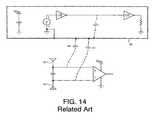
- the manufacturing costis increased by the shield case 28 , and in addition, as shown in an equivalent circuit of FIG. 14 , the intensity of the signal which can be detected from the environment-side electrode 14 and the living body-side electrode 16 is reduced due to influences of parasitic capacitances C 1 and C 2 between the environment-side and living body-side electrodes 14 and 16 and the shield case 28 .
- circuit board 26is not stored in the shield case 28 , but is placed between the environment-side electrode 14 and the living body-side electrode 16 .
- the reception signal of FIG. 16Bis obtained.
- the shield case 28becomes unnecessary and the parasitic capacitance between the environment-side and living body-side electrodes 14 and 16 and the circuit board 26 becomes smaller compared to the case where the shield case 28 is provided, so that the absolute intensity of the reception signal can be increased, but the electromagnetic waves transmitted from the circuit board 26 are superposed as noise on the signal received at the environment-side electrode 14 and the living body-side electrode 16 , and the S/N ratio is degraded.
- the influence of the electromagnetic noise transmitted from the circuit board 26becomes more significant, and the problem of reduction in the S/N of the reception signal becomes more significant.
- a communication systemfor enabling communication between a transmitter which is portable and a receiver which is fixed, using a capacitive coupling through a living body
- the receivercomprises a living body-side electrode which primarily capacitively couples with a living body, an environment-side electrode which primarily capacitively couples with an external environment, and a circuit board on which a circuit which processes a signal which is output from at least one of the living body-side electrode and the environment-side electrode is mounted, and the circuit board is not placed between the living body-side electrode and the environment-side electrode.
- FIG. 1is a diagram showing a structure of a transceiver in a communication system in a preferred embodiment of the present invention
- FIG. 2is a diagram for explaining a communication session using a transceiver of a preferred embodiment of the present invention
- FIG. 3is a diagram showing a structure of another configuration of a transceiver in a communication system of a preferred embodiment of the present invention
- FIG. 4is a diagram showing a placement of an environment-side electrode, a living body-side electrode, and a circuit board of a transceiver of a preferred embodiment of the present invention
- FIG. 5is a diagram showing a placement of an environment-side electrode, a living body-side electrode, and a circuit board of a transceiver of a preferred embodiment of the present invention
- FIG. 6is a diagram showing an equivalent circuit of an environment-side electrode, a living body-side electrode, and a circuit board of a transceiver of a preferred embodiment of the present invention
- FIG. 7is a diagram showing an example of a reception signal of a transceiver of a preferred embodiment of the present invention.
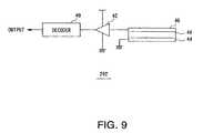
- FIG. 8is a diagram showing a structure of a receiver of a communication system in a preferred embodiment of the present invention.
- FIG. 9is a diagram showing a structure of another example configuration of a receiver of a communication system of a preferred embodiment of the present invention.
- FIG. 10Ais a diagram showing a structure of a transmitter in a communication system of related art
- FIG. 10Bis a diagram showing a structure of a receiver in a communication system of related art
- FIG. 11is a diagram showing an example of formation of an electric field when a communication system is used.
- FIG. 12is a diagram showing an equivalent circuit of a capacitive coupling formed in a communication system
- FIG. 13is a diagram showing a placement of an environment-side electrode, a living body-side electrode, and a circuit board in a transceiver of related art
- FIG. 14is a diagram showing an equivalent circuit of an environment-side electrode, a living body-side electrode, and a circuit board in a transceiver of related art
- FIG. 15is a diagram showing another example placement of an environment-side electrode, a living body-side electrode, and a circuit board in a transceiver of related art
- FIG. 16Ais a diagram showing an example of a reception signal of a communication system of related art
- FIG. 16Bis a diagram showing an example of a reception signal of a communication system of related art
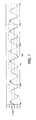
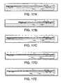
- FIGS. 17A-17Eare diagrams showing a placement of an environment-side electrode, a living body-side electrode, and a circuit board of a transceiver of a preferred embodiment of the present invention
- FIGS. 18A and 18Bare diagrams showing a usage form of a transceiver of a preferred embodiment of the present invention.
- FIG. 19is a diagram showing a placement of an environment-side electrode, a living body-side electrode, and a circuit board of a transceiver of a preferred embodiment of the present invention.
- FIG. 20is a diagram showing a placement of an environment-side electrode, a living body-side electrode, and a circuit board of a transceiver of a preferred embodiment of the present invention.
- a transceiver 200 of a communication system of a preferred embodiment of the present inventioncomprises an encoder 30 , a transmission amplifier 32 , an environment-side electrode 34 , a living body-side electrode 36 , a decoder 40 , a reception amplifier 42 , a changeover switch 44 , and a controller 46 .
- the transceiver 200can be incorporated into a portable electronic device such as a portable phone and a PDA, and used as a portable communication terminal.
- the transceiver 200may be placed in infrastructures such as a ticket barrier in a station, a vending machine, a shop, etc., and used as a communication terminal.
- users carrying portable communication terminals on each of which the transceiver 200 is mountedmay contact or closely place a part of the body, to exchange information between the transceivers 200 .
- a user carrying the portable communication terminal on which the transceiver 200 is mountedmay contact or closely place a part of the body to the living body-side electrode 36 of the transceiver 200 placed in an infrastructure such as a ticket barrier, to exchange data between the transceivers 200 .
- the encoder 30encodes data which is input from the outside using a predetermined encoding method and outputs the encoded data to the transmission amplifier 32 .
- the data which is input from the outsideis input in a superposed state on a base wave of a high frequency.
- the frequency of the base waveis preferably set, for example, to 5 MHz or higher or 15 MHz or lower.
- the transmission amplifier 32comprises a differential amplifier circuit. An inverted input terminal ( ⁇ ) and a non-inverted input terminal (+) of the differential amplifier circuit are connected to an output terminal of the encoder 30 . An inverted output terminal and a non-inverted output terminal of the transmission amplifier 32 are connected to the environment-side electrode 34 and the living body-side electrode 36 through the changeover switch 44 . In the state where the inverted output terminal and the non-inverted output terminal of the transmission amplifier 32 are connected to the environment-side electrode 34 and the living body-side electrode 36 by the changeover switch 44 , the transmission amplifier 32 amplifies a signal which is input from the encoder 30 and differentially outputs to the environment-side electrode 34 and the living body-side electrode 36 . A potential difference between the environment-side electrode 34 and the living body-side electrode 36 changes according to the output of the transmission amplifier 32 .
- the environment-side electrode 34 and the living body-side electrode 36are each formed with a conductor.
- these electrodesare formed in a sheet shape or a plate shape with a conductor such as aluminum, stainless steel, copper foil, copper sheet, etc.
- the environment-side electrode 34 and the living body-side electrode 36are preferably placed in a state electrically insulated from each other, sandwiching a dielectric layer 38 .
- the reception amplifier 42comprises a differential amplifier circuit.
- An inverted input terminal ( ⁇ ) and a non-inverted input terminal (+) of the differential amplifier circuitare connected to the environment-side electrode 34 and the living body-side electrode 36 through the changeover switch 44 .
- An inverted output terminal and a non-inverted output of the differential amplifier circuitare connected to an input terminal of the decoder 40 .
- the reception amplifier 42In the state where the inverted input terminal ( ⁇ ) and the non-inverted input terminal (+) of the reception amplifier 42 are connected to the environment-side electrode 34 and the living body-side electrode 36 by the changeover switch 44 , the reception amplifier 42 amplifies a potential difference between the environment-side electrode 34 and the living body-side electrode 36 and outputs as a potential difference between the inverted output terminal and the non-inverted output terminal.
- the decoder 40receives an output signal from the reception amplifier 42 , decodes the signal using a decoding method corresponding to the encoding method used in the encoder 30 , and outputs the decoded signal.
- the environment-side electrode 34 and the living body-side electrode 36are shared between transmission and reception.
- the controller 46switches the changeover switch 44 to the transmission amplifier 32 when data is to be transmitted and switches the changeover switch 44 to the reception amplifier 42 when data is to be received.
- the timing of the switching of the changeover switch 44may be at a predetermined time period or may be achieved by the user.
- a communication sessioncan be executed by executing a polling process.
- the transceivers 200 provided in the fixed device and the portable deviceperiodically switch between the transmission state and the reception state at a predetermined period.
- the transceiver 200 which is at a transmission sidesends a call to the transceiver 200 which is at a reception side.
- the callis repeated.
- the transceiver 200 of the reception sidecan receive the calling signal from the transceiver 200 of the transmission side
- the transceiver 200 of the reception side receiving the calling signalis activated.
- the activated transceiver 200 of the reception sidetransmits a connection request signal to the transceiver 200 of the transmission side.
- the transceiver 200 of the transmission sideWhen the transceiver 200 of the transmission side receives the connection request signal, the transceiver 200 of the transmission side returns a connection response signal if connection is possible. When the transceiver 200 of the reception side receives the connection response signal, the transceiver 200 of the reception side returns a connection response signal to the transceiver 200 of the transmission side.
- the transceiver 200 of the transmission sidereceives the connection response signal, a data communication session is started. When the communication of data is completed, a completion signal is transmitted from the transceiver 200 of the transmission side to the transceiver 200 of the reception side, and the transceiver 200 of the reception side enters a sleep mode.
- the transceiver 200may have a structure as shown in FIG. 3 .
- the transmission amplifier 32comprises a single amplifier circuit.
- An output terminal of the encoder 30is connected to an input terminal of the amplifier circuit, and an output terminal of the amplifier circuit is connected to the living body-side electrode 36 through the changeover switch 44 .
- the environment-side electrode 34is grounded.
- the transmission amplifier 32amplifies a signal which is input from the encoder 30 and outputs the amplified signal to the living body-side electrode 36 .
- a potential difference between the environment-side electrode 34 and the living body-side electrode 36changes according to an output of the transmission amplifier 32 .
- the reception amplifier 42comprises a single amplifier circuit. An input terminal of the amplifier circuit is connected to the living body-side electrode 36 through the changeover switch 44 , and an output terminal of the amplifier is connected to the decoder 40 .
- the environment-side electrode 34is grounded.
- the reception amplifier 42amplifies a signal which is input from the living body-side electrode 36 and outputs the amplified signal to the decoder 40 .
- the decoder 40decodes the output of the reception amplifier 42 using a decoding method corresponding to the encoding method used in the encoder 30 and outputs the decoded signal.
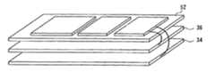
- the transceiver 200 of the present embodimentis mounted in a housing 50 as shown in FIG. 4 .
- Such a configurationis particularly preferable, for example, when the transceiver 200 is used as a portable communication terminal such as a portable phone and a PDA.
- electronic circuits used in the transceiver 200are mounted on a circuit board 52 .
- at least the reception amplifier 42is mounted on the circuit board 52 .
- the encoder 30 , the transmission amplifier 32 , the decoder 40 , the reception amplifier 42 , the changeover switch 44 , and the controller 46are mounted on the circuit board 52 .
- the environment-side electrode 34 , the living body-side electrode 36 , and the circuit board 52are placed in the housing 50 .
- the circuit board 52is placed not in a location sandwiched between the environment-side electrode 34 and the living body-side electrode 36 .
- the circuit board 52is preferably placed at a position where the circuit board 52 is spatially hidden by at least a part of one of the electrodes from at least a part of the other electrode.
- a configurationis employed in which the circuit board 52 , the environment-side electrode 34 , and the living body-side electrode 36 are set to approximately the same size and the circuit board 52 is spatially hidden by one of the electrodes from the other electrode.
- a configurationis employed in which the environment-side electrode 34 and the living body-side electrode 36 are set to approximately the same size, the circuit board 52 is set to a size smaller than the environment-side electrode 34 and the living body-side electrode 36 , and the circuit board 52 is spatially hidden by one of the electrodes from the other electrode.
- FIG. 17Apreferably, a configuration is employed in which the circuit board 52 , the environment-side electrode 34 , and the living body-side electrode 36 are set to approximately the same size and the circuit board 52 is spatially hidden by one of the electrodes from the other electrode.
- a configurationis employed in which one of the environment-side electrode 34 and the living body-side electrode 36 which is placed closer to the circuit board 52 is set to approximately the same size as the circuit board 52 , the other electrode is set to a size smaller than the circuit board 52 , and the circuit board 52 is spatially hidden by the one electrode from the other electrode.
- FIG. 17Dpreferably, a configuration is employed in which the environment-side electrode 34 and the living body-side electrode 36 are set to approximately the same size, the circuit board 52 is set to a size larger than the environment-side electrode 34 and the living body-side electrode 36 , and at least a part of the circuit board 52 is spatially hidden by one of the electrodes from the other electrode.
- reception signal obtained in the structure of the present embodimenthas a higher absolute intensity than the reception signal of FIG. 16A and an improved S/N ratio over the reception signal of FIG. 16B .
- the structure of the transceiver 200 of the present embodimentit is possible to improve the intensity of the reception signal at the reception and to improve S/N ratio of the reception signal.
- the electrode which is placed nearer to the circuit board 52may be set as the environment-side electrode 34 and the other electrode may be set as the living body-side electrode 36 .
- the electrode placed nearer to the circuit board 52may be set as the living body-side electrode 36 and the other electrode maybe set as the environment-side electrode 34 .
- the phase of the reception signal during usagewould be inverted.
- a modulation method which does not depend on phase inversionsuch as PSK, FSK, and ASK, it is possible to use in the reverse direction.
- the names of the environment-side electrode 34 and the living body-side electrode 36are only for the purpose of convenience, and the electrodes may be used in the opposite configuration.
- the dielectric layer 38 which functions as an antenna and which is sandwiched between the environment-side electrode 34 and the living body-side electrode 36is not limited to a resin such as epoxy, and an insulating material similar to the circuit board 52 or a foam resin having a low dielectric constant may be used.
- the housing of the electronic devicesuch as the portable phone is made of an insulating member, as shown in FIG. 20
- a structuremay be employed in which the housing itself is used as the dielectric layer 38 and sandwiched by the environment-side electrode 34 and the living body-side electrode 36 .
- a transceiver 200 having both the transmission system and reception systemis exemplified, but the present invention is not limited to such a configuration, and may be applied to a communication system in which a transmitter of a transmission system and a receiver of a reception system are separately formed.
- the circuit boardmay be provided not sandwiched between the environment-side electrode 44 and the living body-side electrode 46 , to obtain similar advantages.
- a configurationmay be employed in which the reception amplifier 42 is changed from the differential amplifier circuit to a single amplifier circuit.
Landscapes
- Engineering & Computer Science (AREA)
- Computer Networks & Wireless Communication (AREA)
- Signal Processing (AREA)
- Near-Field Transmission Systems (AREA)
- Transceivers (AREA)
Abstract
Description
Claims (5)
Applications Claiming Priority (2)
| Application Number | Priority Date | Filing Date | Title |
|---|---|---|---|
| JP2008155013AJP5290633B2 (en) | 2008-06-13 | 2008-06-13 | Communication system and receiving apparatus used therefor |
| JP2008-155013 | 2008-06-13 |
Publications (2)
| Publication Number | Publication Date |
|---|---|
| US20090309708A1 US20090309708A1 (en) | 2009-12-17 |
| US8452234B2true US8452234B2 (en) | 2013-05-28 |
Family
ID=41414217
Family Applications (1)
| Application Number | Title | Priority Date | Filing Date |
|---|---|---|---|
| US12/484,817Active2032-03-28US8452234B2 (en) | 2008-06-13 | 2009-06-15 | Communication system and receiver used in communication system |
Country Status (3)
| Country | Link |
|---|---|
| US (1) | US8452234B2 (en) |
| JP (1) | JP5290633B2 (en) |
| CN (1) | CN101604988B (en) |
Cited By (9)
| Publication number | Priority date | Publication date | Assignee | Title |
|---|---|---|---|---|
| US20140057562A1 (en)* | 2010-11-19 | 2014-02-27 | Kabushiki Kaisha Toshiba | Communication apparatus and communication system |
| US20160149313A1 (en)* | 2014-11-24 | 2016-05-26 | Nxp, B.V. | Electromagnetic field induction for inter-body and transverse body communication |
| US9819097B2 (en) | 2015-08-26 | 2017-11-14 | Nxp B.V. | Antenna system |
| US9819395B2 (en) | 2014-05-05 | 2017-11-14 | Nxp B.V. | Apparatus and method for wireless body communication |
| US9819075B2 (en) | 2014-05-05 | 2017-11-14 | Nxp B.V. | Body communication antenna |
| US10009069B2 (en) | 2014-05-05 | 2018-06-26 | Nxp B.V. | Wireless power delivery and data link |
| US10015604B2 (en) | 2014-05-05 | 2018-07-03 | Nxp B.V. | Electromagnetic induction field communication |
| US10014578B2 (en) | 2014-05-05 | 2018-07-03 | Nxp B.V. | Body antenna system |
| US10320086B2 (en) | 2016-05-04 | 2019-06-11 | Nxp B.V. | Near-field electromagnetic induction (NFEMI) antenna |
Families Citing this family (13)
| Publication number | Priority date | Publication date | Assignee | Title |
|---|---|---|---|---|
| JP5431960B2 (en) | 2007-12-07 | 2014-03-05 | 大同塗料株式会社 | Method for producing carbon nanotube-containing conductor |
| JP4616379B2 (en)* | 2008-09-24 | 2011-01-19 | 日本電信電話株式会社 | Mobile phone |
| BR112012019212A2 (en)* | 2010-02-01 | 2017-06-13 | Proteus Digital Health Inc | data collection system |
| JP2012053520A (en)* | 2010-08-31 | 2012-03-15 | Nippon Signal Co Ltd:The | Entrance/exit management system and human body communication unit |
| FR2973183A1 (en)* | 2011-03-21 | 2012-09-28 | France Telecom | WIRELESS COMMUNICATION DEVICE AND METHOD |
| JP2014135633A (en)* | 2013-01-10 | 2014-07-24 | Toyo Ink Sc Holdings Co Ltd | Receiver for human body communication |
| JP6498177B2 (en) | 2013-03-15 | 2019-04-10 | プロテウス デジタル ヘルス, インコーポレイテッド | Identity authentication system and method |
| CA2965941C (en) | 2013-09-20 | 2020-01-28 | Proteus Digital Health, Inc. | Methods, devices and systems for receiving and decoding a signal in the presence of noise using slices and warping |
| JP6238351B2 (en)* | 2013-12-12 | 2017-11-29 | パナソニック株式会社 | Human body communication device |
| US9667354B2 (en)* | 2014-11-24 | 2017-05-30 | Sony Corporation | Situational based communication |
| FR3044495A1 (en)* | 2015-11-30 | 2017-06-02 | Orange | WIRELESS COMMUNICATION DEVICE AND METHOD |
| US10911159B2 (en) | 2016-10-13 | 2021-02-02 | Sony Corporation | Communication unit and communication system |
| EP3528404A4 (en)* | 2016-10-13 | 2019-10-09 | Sony Semiconductor Solutions Corporation | Communications device and communications system |
Citations (13)
| Publication number | Priority date | Publication date | Assignee | Title |
|---|---|---|---|---|
| US5914701A (en)* | 1995-05-08 | 1999-06-22 | Massachusetts Institute Of Technology | Non-contact system for sensing and signalling by externally induced intra-body currents |
| US6104913A (en)* | 1998-03-11 | 2000-08-15 | Bell Atlantic Network Services, Inc. | Personal area network for personal telephone services |
| US6211799B1 (en) | 1997-11-06 | 2001-04-03 | Massachusetts Institute Of Technology | Method and apparatus for transbody transmission of power and information |
| US6223018B1 (en)* | 1996-12-12 | 2001-04-24 | Nippon Telegraph And Telephone Corporation | Intra-body information transfer device |
| JP2001308803A (en) | 2000-04-26 | 2001-11-02 | Matsushita Electric Works Ltd | Data communication system, security system for apparatus utilizing the system, and portable telephone and portable information terminal utilizing the data communication system or the security system |
| JP2002009710A (en) | 2000-06-26 | 2002-01-11 | Matsushita Electric Works Ltd | Data transmission system utilizing human body as signal transmission path |
| US6859657B1 (en)* | 1998-08-29 | 2005-02-22 | Koninklijke Philips Electronics N.V. | Personal communications apparatus |
| US6965842B2 (en)* | 2001-06-01 | 2005-11-15 | Sony Corporation | User input apparatus |
| JP2008027219A (en) | 2006-07-21 | 2008-02-07 | Sony Corp | Information processing system, receiving device and method, recording medium, and program |
| US20080261523A1 (en)* | 2005-05-17 | 2008-10-23 | Fumio Kubono | Communication Device and Method, and Program |
| US7509092B2 (en)* | 2005-05-17 | 2009-03-24 | Sony Corporation | Information processing system and information processing method |
| US20090325485A1 (en)* | 2008-06-13 | 2009-12-31 | Sanyo Electric Co., Ltd. | Communication system and receiver used in communication system |
| US7860455B2 (en)* | 2002-07-18 | 2010-12-28 | Ntt Docomo, Inc. | Electronic communications system, apparatus and electrode layout method |
Family Cites Families (1)
| Publication number | Priority date | Publication date | Assignee | Title |
|---|---|---|---|---|
| KR100522132B1 (en)* | 2003-01-25 | 2005-10-18 | 한국과학기술연구원 | Data receiving method and apparatus in human body communication system |
- 2008
- 2008-06-13JPJP2008155013Apatent/JP5290633B2/ennot_activeExpired - Fee Related
- 2009
- 2009-06-11CNCN2009101595390Apatent/CN101604988B/ennot_activeExpired - Fee Related
- 2009-06-15USUS12/484,817patent/US8452234B2/enactiveActive
Patent Citations (13)
| Publication number | Priority date | Publication date | Assignee | Title |
|---|---|---|---|---|
| US5914701A (en)* | 1995-05-08 | 1999-06-22 | Massachusetts Institute Of Technology | Non-contact system for sensing and signalling by externally induced intra-body currents |
| US6223018B1 (en)* | 1996-12-12 | 2001-04-24 | Nippon Telegraph And Telephone Corporation | Intra-body information transfer device |
| US6211799B1 (en) | 1997-11-06 | 2001-04-03 | Massachusetts Institute Of Technology | Method and apparatus for transbody transmission of power and information |
| US6104913A (en)* | 1998-03-11 | 2000-08-15 | Bell Atlantic Network Services, Inc. | Personal area network for personal telephone services |
| US6859657B1 (en)* | 1998-08-29 | 2005-02-22 | Koninklijke Philips Electronics N.V. | Personal communications apparatus |
| JP2001308803A (en) | 2000-04-26 | 2001-11-02 | Matsushita Electric Works Ltd | Data communication system, security system for apparatus utilizing the system, and portable telephone and portable information terminal utilizing the data communication system or the security system |
| JP2002009710A (en) | 2000-06-26 | 2002-01-11 | Matsushita Electric Works Ltd | Data transmission system utilizing human body as signal transmission path |
| US6965842B2 (en)* | 2001-06-01 | 2005-11-15 | Sony Corporation | User input apparatus |
| US7860455B2 (en)* | 2002-07-18 | 2010-12-28 | Ntt Docomo, Inc. | Electronic communications system, apparatus and electrode layout method |
| US20080261523A1 (en)* | 2005-05-17 | 2008-10-23 | Fumio Kubono | Communication Device and Method, and Program |
| US7509092B2 (en)* | 2005-05-17 | 2009-03-24 | Sony Corporation | Information processing system and information processing method |
| JP2008027219A (en) | 2006-07-21 | 2008-02-07 | Sony Corp | Information processing system, receiving device and method, recording medium, and program |
| US20090325485A1 (en)* | 2008-06-13 | 2009-12-31 | Sanyo Electric Co., Ltd. | Communication system and receiver used in communication system |
Non-Patent Citations (5)
| Title |
|---|
| "Personal Area Networks (PAN): Near-Field Intra-Body Communication", Thomas Guthrie Zimmerman, B.S., Humanities and Engineering Massachusetts Institute of Technology (1980). |
| Nikkei Electronics Jun. 2, 1997 (No. 690) pp. 141-148, Corresponds to English Version Referenced in Non-Patent Literature Documents, Cite No. 1. |
| Notice of Grounds for Rejection for Japanese Patent Application No. 2008-155013, mailed Oct. 30, 2012, with English translation. |
| Notice of Grounds for Rejection for Patent Application Serial No. 2008-155013, mailed Jul. 24, 2012, with English translation. |
| The First Office Action for Chinese Patent Application No. 200910159539.0, issued Mar. 12, 2012, with English translation. |
Cited By (11)
| Publication number | Priority date | Publication date | Assignee | Title |
|---|---|---|---|---|
| US20140057562A1 (en)* | 2010-11-19 | 2014-02-27 | Kabushiki Kaisha Toshiba | Communication apparatus and communication system |
| US9014629B2 (en)* | 2010-11-19 | 2015-04-21 | Kabushiki Kaisha Toshiba | Communication apparatus and communication system |
| US9819395B2 (en) | 2014-05-05 | 2017-11-14 | Nxp B.V. | Apparatus and method for wireless body communication |
| US9819075B2 (en) | 2014-05-05 | 2017-11-14 | Nxp B.V. | Body communication antenna |
| US10009069B2 (en) | 2014-05-05 | 2018-06-26 | Nxp B.V. | Wireless power delivery and data link |
| US10015604B2 (en) | 2014-05-05 | 2018-07-03 | Nxp B.V. | Electromagnetic induction field communication |
| US10014578B2 (en) | 2014-05-05 | 2018-07-03 | Nxp B.V. | Body antenna system |
| US20160149313A1 (en)* | 2014-11-24 | 2016-05-26 | Nxp, B.V. | Electromagnetic field induction for inter-body and transverse body communication |
| US9812788B2 (en)* | 2014-11-24 | 2017-11-07 | Nxp B.V. | Electromagnetic field induction for inter-body and transverse body communication |
| US9819097B2 (en) | 2015-08-26 | 2017-11-14 | Nxp B.V. | Antenna system |
| US10320086B2 (en) | 2016-05-04 | 2019-06-11 | Nxp B.V. | Near-field electromagnetic induction (NFEMI) antenna |
Also Published As
| Publication number | Publication date |
|---|---|
| JP5290633B2 (en) | 2013-09-18 |
| JP2009302895A (en) | 2009-12-24 |
| US20090309708A1 (en) | 2009-12-17 |
| CN101604988A (en) | 2009-12-16 |
| CN101604988B (en) | 2012-10-24 |
Similar Documents
| Publication | Publication Date | Title |
|---|---|---|
| US8452234B2 (en) | Communication system and receiver used in communication system | |
| JP5166131B2 (en) | Communication system and receiving apparatus used therefor | |
| CN102646861B (en) | Antenna with integrated proximity sensor for proximity-based radio-frequency power control | |
| KR102074947B1 (en) | NFC antenna module and NFC module including the same | |
| CN108270088B (en) | Antenna assembly, electronic equipment and antenna switching method | |
| US9948404B2 (en) | Channel adaptive human body communication system | |
| US20070066274A1 (en) | Antenna integrated speaker assembly, manufacturing method thereof, and wireless communication device having the same | |
| US9966651B2 (en) | Antenna and wireless communication device using the same | |
| KR20090010431A (en) | Mobile communication terminal | |
| WO2003095023A3 (en) | Passive telemetry system for implantable medical device | |
| EP1162753A3 (en) | Communication apparatus and portable telephone | |
| KR20100075353A (en) | Communication system and mehtod using a part of human body as an antenna in the body area network | |
| US8208852B2 (en) | Electronic apparatus for electric field communication | |
| US9876276B2 (en) | Device with radio and body-coupled-communication connectivity | |
| CN108666741B (en) | Antenna components and electronic equipment | |
| JP2003124728A (en) | Antenna device, communication module and electronic equipment | |
| KR20090116866A (en) | Handheld terminal with antenna mounted on side key FPC | |
| WO2006073637A3 (en) | Wireless communication device antenna for improved communication with a satellite | |
| US8489027B2 (en) | Method and apparatus for communicating sound wave of human body | |
| JP3592460B2 (en) | Printed wiring board and radio | |
| JP2010074797A (en) | Communication system | |
| JP4053367B2 (en) | Portable wireless communication device | |
| KR20070109025A (en) | Antenna for mobile communication terminal with video receiving function | |
| CN208386610U (en) | Fingerprint recognition mould group and electronic equipment with it | |
| JP4305599B2 (en) | Portable radio with built-in variable antenna matching circuit |
Legal Events
| Date | Code | Title | Description |
|---|---|---|---|
| AS | Assignment | Owner name:SANYO ELECTRIC CO., LTD., JAPAN Free format text:ASSIGNMENT OF ASSIGNORS INTEREST;ASSIGNORS:HASEGAWA, KAZUO;SUZUKI, HIROHISA;REEL/FRAME:022848/0668 Effective date:20090603 Owner name:SANYO SEMICONDUCTOR CO., LTD., JAPAN Free format text:ASSIGNMENT OF ASSIGNORS INTEREST;ASSIGNORS:HASEGAWA, KAZUO;SUZUKI, HIROHISA;REEL/FRAME:022848/0668 Effective date:20090603 | |
| AS | Assignment | Owner name:SEMICONDUCTOR COMPONENTS INDUSTRIES, LLC, ARIZONA Free format text:ASSIGNMENT OF ASSIGNORS INTEREST;ASSIGNOR:SANYO ELECTRIC CO., LTD.;REEL/FRAME:026594/0385 Effective date:20110101 | |
| STCF | Information on status: patent grant | Free format text:PATENTED CASE | |
| AS | Assignment | Owner name:SEMICONDUCTOR COMPONENTS INDUSTRIES, LLC, ARIZONA Free format text:CORRECTIVE ASSIGNMENT TO CORRECT THE INCORRECT #12/577882 PREVIOUSLY RECORDED ON REEL 026594 FRAME 0385. ASSIGNOR(S) HEREBY CONFIRMS THE ASSIGNMENT;ASSIGNOR:SANYO ELECTRIC CO., LTD;REEL/FRAME:032836/0342 Effective date:20110101 | |
| AS | Assignment | Owner name:SEMICONDUCTOR COMPONENTS INDUSTRIES, LLC, ARIZONA Free format text:ASSIGNMENT OF ASSIGNORS INTEREST;ASSIGNOR:SANYO SEMICONDUCTOR CO., LTD.;REEL/FRAME:033813/0420 Effective date:20140924 | |
| AS | Assignment | Owner name:SYSTEM SOLUTIONS CO., LTD., JAPAN Free format text:CHANGE OF NAME;ASSIGNOR:SANYO SEMICONDUCTOR CO., LTD;REEL/FRAME:034537/0044 Effective date:20140228 | |
| AS | Assignment | Owner name:SEMICONDUCTOR COMPONENTS INDUSTRIES, LLC, ARIZONA Free format text:CORRECTIVE ASSIGNMENT TO CORRECT THE ASSIGNOR NAME PREVIOUSLY RECORDED AT REEL: 033813 FRAME: 0420. ASSIGNOR(S) HEREBY CONFIRMS THE ASSIGNMENT;ASSIGNOR:SYSTEM SOLUTIONS CO., LTD.;REEL/FRAME:034816/0510 Effective date:20141217 | |
| AS | Assignment | Owner name:DEUTSCHE BANK AG NEW YORK BRANCH, NEW YORK Free format text:SECURITY INTEREST;ASSIGNOR:SEMICONDUCTOR COMPONENTS INDUSTRIES, LLC;REEL/FRAME:038620/0087 Effective date:20160415 | |
| AS | Assignment | Owner name:DEUTSCHE BANK AG NEW YORK BRANCH, AS COLLATERAL AG Free format text:CORRECTIVE ASSIGNMENT TO CORRECT THE INCORRECT PATENT NUMBER 5859768 AND TO RECITE COLLATERAL AGENT ROLE OF RECEIVING PARTY IN THE SECURITY INTEREST PREVIOUSLY RECORDED ON REEL 038620 FRAME 0087. ASSIGNOR(S) HEREBY CONFIRMS THE SECURITY INTEREST;ASSIGNOR:SEMICONDUCTOR COMPONENTS INDUSTRIES, LLC;REEL/FRAME:039853/0001 Effective date:20160415 Owner name:DEUTSCHE BANK AG NEW YORK BRANCH, AS COLLATERAL AGENT, NEW YORK Free format text:CORRECTIVE ASSIGNMENT TO CORRECT THE INCORRECT PATENT NUMBER 5859768 AND TO RECITE COLLATERAL AGENT ROLE OF RECEIVING PARTY IN THE SECURITY INTEREST PREVIOUSLY RECORDED ON REEL 038620 FRAME 0087. ASSIGNOR(S) HEREBY CONFIRMS THE SECURITY INTEREST;ASSIGNOR:SEMICONDUCTOR COMPONENTS INDUSTRIES, LLC;REEL/FRAME:039853/0001 Effective date:20160415 | |
| FPAY | Fee payment | Year of fee payment:4 | |
| MAFP | Maintenance fee payment | Free format text:PAYMENT OF MAINTENANCE FEE, 8TH YEAR, LARGE ENTITY (ORIGINAL EVENT CODE: M1552); ENTITY STATUS OF PATENT OWNER: LARGE ENTITY Year of fee payment:8 | |
| AS | Assignment | Owner name:FAIRCHILD SEMICONDUCTOR CORPORATION, ARIZONA Free format text:RELEASE OF SECURITY INTEREST IN PATENTS RECORDED AT REEL 038620, FRAME 0087;ASSIGNOR:DEUTSCHE BANK AG NEW YORK BRANCH, AS COLLATERAL AGENT;REEL/FRAME:064070/0001 Effective date:20230622 Owner name:SEMICONDUCTOR COMPONENTS INDUSTRIES, LLC, ARIZONA Free format text:RELEASE OF SECURITY INTEREST IN PATENTS RECORDED AT REEL 038620, FRAME 0087;ASSIGNOR:DEUTSCHE BANK AG NEW YORK BRANCH, AS COLLATERAL AGENT;REEL/FRAME:064070/0001 Effective date:20230622 | |
| MAFP | Maintenance fee payment | Free format text:PAYMENT OF MAINTENANCE FEE, 12TH YEAR, LARGE ENTITY (ORIGINAL EVENT CODE: M1553); ENTITY STATUS OF PATENT OWNER: LARGE ENTITY Year of fee payment:12 |